
Gate questions ec04 2014 praveen someh
19
GATE 2014: General Instructions during Examination 1. Total duration of the GATE examination is 180 minutes. 2. The clock will be set at the server. The countdown timer at the top right corner of screen will display the remaining time available for you to complete the examination. When the timer reaches zero, the examination will end by itself. You need not terminate the examination or submit your paper. 3. Any useful data required for your paper can be viewed by clicking on the Useful Common Data button that appears on the screen. 4. Use the scribble pad provided to you for any rough work. Submit the scribble pad at the end of the examination. 5. You are allowed to use a non-programmable type calculator, however, sharing of calculators is not allowed. 6. The Question Palette displayed on the right side of screen will show the status of each question using one of the following symbols: The Marked for Review status for a question simply indicates that you would like to look at that question again. If a question is answered, but marked for review, then the answer will be considered for evaluation unless the status is modified by the candidate. Navigating to a Question : 7. To answer a question, do the following: a. Click on the question number in the Question Palette to go to that question directly. b. Select an answer for a multiple choice type question by clicking on the bubble placed before the 4 choices, namely A, B, C and D. Use the virtual numeric keypad to enter a number as answer for a numerical type question. c. Click on Save & Next to save your answer for the current question and then go to the next question. d. Click on Mark for Review & Next to save your answer for the current question and also mark it for review, and then go to the next question. www.jntuworld.com || www.android.jntuworld.com || www.jwjobs.net || www.android.jwjobs.net www.jntuworld.com || www.jwjobs.net
-
Upload
praveensomesh -
Category
Engineering
-
view
127 -
download
10
Transcript of Gate questions ec04 2014 praveen someh

GATE 2014: General Instructions during Examination
1. Total duration of the GATE examination is 180 minutes. 2. The clock will be set at the server. The countdown timer at the top right corner of
screen will display the remaining time available for you to complete the examination. When the timer reaches zero, the examination will end by itself. You need not terminate the examination or submit your paper.
3. Any useful data required for your paper can be viewed by clicking on the Useful Common Data button that appears on the screen.
4. Use the scribble pad provided to you for any rough work. Submit the scribble pad at the end of the examination.
5. You are allowed to use a non-programmable type calculator, however, sharing of calculators is not allowed.
6. The Question Palette displayed on the right side of screen will show the status of each question using one of the following symbols:
The Marked for Review status for a question simply indicates that you would like to look at that question again. If a question is answered, but marked for review, then the answer will be considered for evaluation unless the status is modified by the candidate.
Navigating to a Question :
7. To answer a question, do the following: a. Click on the question number in the Question Palette to go to that question
directly. b. Select an answer for a multiple choice type question by clicking on the bubble
placed before the 4 choices, namely A, B, C and D. Use the virtual numeric keypad to enter a number as answer for a numerical type question.
c. Click on Save & Next to save your answer for the current question and then go to the next question.
d. Click on Mark for Review & Next to save your answer for the current question and also mark it for review, and then go to the next question.
www.jntuworld.com || www.android.jntuworld.com || www.jwjobs.net || www.android.jwjobs.net
www.jntuworld.com || www.jwjobs.net

Caution: Note that your answer for the current question will not be saved, if you navigate to another question directly by clicking on a question number without saving the answer to the previous question.
You can view all the questions by clicking on the Question Paper button. This feature is provided, so that if you want you can just see the entire question paper at a glance.
Answering a Question :
8. Procedure for answering a multiple choice (MCQ) type question: a. Choose one answer from the 4 options (A,B,C,D) given below the question,
click on the bubble placed before the chosen option. b. To deselect your chosen answer, click on the bubble of the chosen option again
or click on the Clear Response button. c. To change your chosen answer, click on the bubble of another option. d. To save your answer, you MUST click on the Save & Next button.
9. Procedure for answering a numerical answer type question: a. To enter a number as your answer, use the virtual numerical keypad. b. A fraction (e.g. -0.3 or -.3) can be entered as an answer with or without '0'
before the decimal point. As many as four decimal points, e.g. 12.5435 or 0.003 or -932.6711 or 12.82 can be entered.
c. To clear your answer, click on the Clear Response button. d. To save your answer, you MUST click on the Save & Next button
10. To mark a question for review, click on the Mark for Review & Next button. If an answer is selected (for MCQ) or entered (for numerical answer type) for a question that is Marked for Review, that answer will be considered in the evaluation unless the status is modified by the candidate.
11. To change your answer to a question that has already been answered, first select that question for answering and then follow the procedure for answering that type of question.
12. Note that ONLY Questions for which answers are saved or marked for review after answering will be considered for evaluation.
Choosing a Section :
13. Sections in this question paper are displayed on the top bar of the screen. Questions in a Section can be viewed by clicking on the name of that Section. The Section you are currently viewing will be highlighted.
14. A checkbox is displayed for every optional Section, if any, in the Question Paper. To select the optional Section for answering, click on the checkbox for that Section.
15. If the checkbox for an optional Section is not selected, the Save & Next button and the Mark for Review & Next button will NOT be enabled for that Section. You will
www.jntuworld.com || www.android.jntuworld.com || www.jwjobs.net || www.android.jwjobs.net
www.jntuworld.com || www.jwjobs.net
only be able to see questions in this Section, but you will not be able to answer questions in the Section.
16. After clicking the Save & Next button for the last question in a Section, you will automatically be taken to the first question of the next Section in sequence.
17. You can move the mouse cursor over the name of a Section to view the answering status for that Section.
Changing the Optional Section :
18. After answering the chosen optional Section, partially or completely, you can change the optional Section by selecting the checkbox for a new Section that you want to attempt. A warning message will appear along with a table showing the number of questions answered in each of the previously chosen optional Sections and a checkbox against each of these Sections. Click on a checkbox against a Section that you want to reset and then click on the RESET button. Note that RESETTING a Section will DELETE all the answers for questions in that Section. Hence, if you think that you may want to select this Section again later, you will have to note down your answers for questions in that Section. If you do not want to reset the Section and want to continue answering the previously chosen optional Section, then click on the BACK button.
19. If you deselect the checkbox for an optional Section in the top bar, the following warning message will appear: "Deselecting the checkbox will DELETE all the answers for questions in this Section. Do you want to deselect this Section?” If you want to deselect, click on the RESET button. If you do not want to deselect, click on the BACK button.
20. You can shuffle between different Sections or change the optional Sections any number of times.
www.jntuworld.com || www.android.jntuworld.com || www.jwjobs.net || www.android.jwjobs.net
www.jntuworld.com || www.jwjobs.net

GATE 2014 Examination
EC: Electronics & Communications Engineering Duration: 180 minutes Maximum Marks: 100
Read the following instructions carefully.
1. To login, enter your Registration Number and password provided to you. Kindly go through the various symbols used in the test and understand their meaning before you start the examination.
2. Once you login and after the start of the examination, you can view all the questions in the question paper, by clicking on the View All Questions button in the screen.
3. This question paper consists of 2 sections, General Aptitude (GA) for 15 marks and the subject specific GATE paper for 85 marks. Both these sections are compulsory. The GA section consists of 10 questions. Question numbers 1 to 5 are of 1-mark each, while question numbers 6 to 10 are of 2-mark each. The subject specific GATE paper section consists of 55 questions, out of which question numbers 1 to 25 are of 1-mark each, while question numbers 26 to 55 are of 2-mark each.
4. Depending upon the GATE paper, there may be useful common data that may be required for answering the questions. If the paper has such useful data, the same can be viewed by clicking on the Useful Common Data button that appears at the top, right hand side of the screen.
5. The computer allotted to you at the examination center runs specialized software that permits only one answer to be selected for multiple-choice questions using a mouse and to enter a suitable number for the numerical answer type questions using the virtual keyboard and mouse.
6. Your answers shall be updated and saved on a server periodically and also at the end of the examination. The examination will stop automatically at the end of 180 minutes.
7. In each paper a candidate can answer a total of 65 questions carrying 100 marks. 8. The question paper may consist of questions of multiple choice type (MCQ) and numerical answer
type. 9. Multiple choice type questions will have four choices against A, B, C, D, out of which only ONE is the
correct answer. The candidate has to choose the correct answer by clicking on the bubble (⃝) placed before the choice.
10. For numerical answer type questions, each question will have a numerical answer and there will not be any choices. For these questions, the answer should be enteredby using the virtual keyboard that appears on the monitor and the mouse.
11. All questions that are not attempted will result in zero marks. However, wrong answers for multiple choice type questions (MCQ) will result in NEGATIVE marks. For all MCQ questions a wrong answer will result in deduction of⅓ marks for a 1-mark question and ⅔ marks for a 2-mark question.
12. There is NO NEGATIVE MARKING for questions of NUMERICAL ANSWER TYPE.
13. Non-programmable type Calculator is allowed. Charts, graph sheets, and mathematical tables are NOT allowed in the Examination Hall. You must use the Scribble pad provided to you at the examination centre for all your rough work. The Scribble Pad has to be returned at the end of the examination.
Declaration by the candidate: “I have read and understood all the above instructions. I have also read and understood clearly the instructions given on the admit card and shall follow the same. I also understand that in case I am found to violate any of these instructions, my candidature is liable to be cancelled. I also confirm that at the start of the examination all the computer hardware allotted to me are in proper working condition”.
www.jntuworld.com || www.android.jntuworld.com || www.jwjobs.net || www.android.jwjobs.net
www.jntuworld.com || www.jwjobs.net
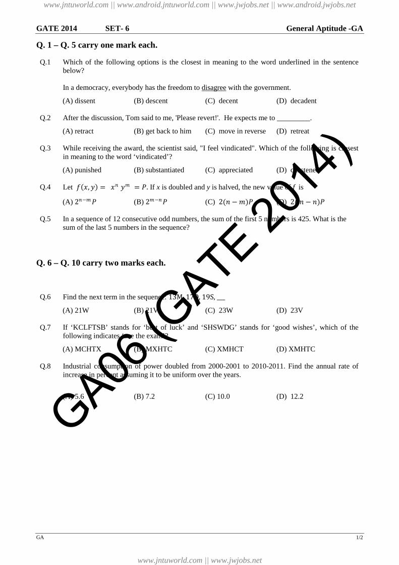
GATE 2014 SET- 6 General Aptitude -GA
GA 1/2
Q. 1 – Q. 5 carry one mark each.
Q.1 Which of the following options is the closest in meaning to the word underlined in the sentence below? In a democracy, everybody has the freedom to disagree with the government.
(A) dissent (B) descent (C) decent (D) decadent Q.2 After the discussion, Tom said to me, 'Please revert!'. He expects me to _________.
(A) retract (B) get back to him (C) move in reverse (D) retreat Q.3 While receiving the award, the scientist said, "I feel vindicated". Which of the following is closest
in meaning to the word ‘vindicated’?
(A) punished (B) substantiated (C) appreciated (D) chastened Q.4 Let 𝑓𝑓(𝑥𝑥,𝑦𝑦) = 𝑥𝑥𝑛𝑛 𝑦𝑦𝑚𝑚 = 𝑃𝑃. If x is doubled and y is halved, the new value of f is
(A) 2𝑛𝑛−𝑚𝑚𝑃𝑃 (B) 2𝑚𝑚−𝑛𝑛𝑃𝑃 (C) 2(𝑛𝑛 −𝑚𝑚)𝑃𝑃 (D) 2(𝑚𝑚 − 𝑛𝑛)𝑃𝑃 Q.5 In a sequence of 12 consecutive odd numbers, the sum of the first 5 numbers is 425. What is the
sum of the last 5 numbers in the sequence?
Q. 6 – Q. 10 carry two marks each.
Q.6 Find the next term in the sequence: 13M, 17Q, 19S, ___
(A) 21W (B) 21V (C) 23W (D) 23V Q.7 If ‘KCLFTSB’ stands for ‘best of luck’ and ‘SHSWDG’ stands for ‘good wishes’, which of the
following indicates ‘ace the exam’?
(A) MCHTX (B) MXHTC (C) XMHCT (D) XMHTC Q.8 Industrial consumption of power doubled from 2000-2001 to 2010-2011. Find the annual rate of
increase in percent assuming it to be uniform over the years.
(A) 5.6 (B) 7.2 (C) 10.0 (D) 12.2 GA06
(GATE 20
14)
www.jntuworld.com || www.android.jntuworld.com || www.jwjobs.net || www.android.jwjobs.net
www.jntuworld.com || www.jwjobs.net

GATE 2014 SET- 6 General Aptitude -GA
GA 2/2
Q.9 A firm producing air purifiers sold 200 units in 2012. The following pie chart presents the share of raw material, labour, energy, plant & machinery, and transportation costs in the total manufacturing cost of the firm in 2012. The expenditure on labour in 2012 is Rs. 4,50,000. In 2013, the raw material expenses increased by 30% and all other expenses increased by 20%. What is the percentage increase in total cost for the company in 2013?
Q.10 A five digit number is formed using the digits 1,3,5,7 and 9 without repeating any of them. What is
the sum of all such possible five digit numbers?
(A) 6666660 (B) 6666600 (C) 6666666 (D) 6666606
END OF THE QUESTION PAPER
GA06 (G
ATE 2014
)
www.jntuworld.com || www.android.jntuworld.com || www.jwjobs.net || www.android.jwjobs.net
www.jntuworld.com || www.jwjobs.net

GATE 2014 SET4 ELECTRONICS AND COMMUNICATION ENGINEERING – EC
EC 1/13
Q. 1 – Q. 25 carry one mark each.
Q.1 The series ∑ 1𝑛𝑛!
∞𝑛𝑛=0 converges to
(A) 2 ln 2 (B) √2 (C) 2 (D) 𝑒𝑒 Q.2 The magnitude of the gradient for the function 𝑓𝑓(𝑥𝑥,𝑦𝑦, 𝑧𝑧) = 𝑥𝑥2 + 3𝑦𝑦2 + 𝑧𝑧3 at the point (1,1,1)
is _________.
Q.3 Let 𝑋𝑋 be a zero mean unit variance Gaussian random variable. 𝐸𝐸[|𝑋𝑋|] is equal to _____
Q.4 If 𝑎𝑎 and 𝑏𝑏 are constants, the most general solution of the differential equation
𝑑𝑑2𝑥𝑥𝑑𝑑𝑡𝑡2 + 2
𝑑𝑑𝑥𝑥𝑑𝑑𝑡𝑡
+ 𝑥𝑥 = 0 is
(A) 𝑎𝑎𝑒𝑒−𝑡𝑡 (B) 𝑎𝑎𝑒𝑒−𝑡𝑡 + 𝑏𝑏𝑡𝑡𝑒𝑒−𝑡𝑡 (C) 𝑎𝑎𝑒𝑒𝑡𝑡 + 𝑏𝑏𝑡𝑡𝑒𝑒−𝑡𝑡 (D) 𝑎𝑎𝑒𝑒−2𝑡𝑡 Q.5
The directional derivative of ( )( , )2
xyf x y x y= + at (1, 1) in the direction of the unit vector at an
angle of 4π
with y-axis, is given by ______ .
Q.6 The circuit shown in the figure represents a
(A) voltage controlled voltage source (B) voltage controlled current source (C) current controlled current source (D) current controlled voltage source
Q.7 The magnitude of current (in mA) through the resistor R2 in the figure shown is_______.
Ii R
AIIi
EC04 (G
ATE 2014
)
www.jntuworld.com || www.android.jntuworld.com || www.jwjobs.net || www.android.jwjobs.net
www.jntuworld.com || www.jwjobs.net

GATE 2014 SET4 ELECTRONICS AND COMMUNICATION ENGINEERING – EC
EC 2/13
Q.8 At T = 300 K, the band gap and the intrinsic carrier concentration of GaAs are 1.42 eV and 106 cm-3, respectively. In order to generate electron hole pairs in GaAs, which one of the wavelength (λC) ranges of incident radiation, is most suitable? (Given that: Plank’s constant is 6.62 × 10⁻³⁴ J-s, velocity of light is 3 × 1010 cm/s and charge of electron is 1.6 × 10⁻¹⁹ C)
(A) 0.42 µm < λC < 0.87 µm (B) 0.87 µm < λC < 1.42 µm (C) 1.42 µm < λC < 1.62 µm (D) 1.62 µm < λC < 6.62 µm
Q.9 In the figure, ln (ρi) is plotted as a function of 1/T, where ρi is the intrinsic resistivity of silicon, T
is the temperature, and the plot is almost linear.
ln (ρi)
1 / T The slope of the line can be used to estimate
(A) band gap energy of silicon (Eg) (B) sum of electron and hole mobility in silicon (µn + µp) (C) reciprocal of the sum of electron and hole mobility in silicon (µn + µp) -1 (D) intrinsic carrier concentration of silicon (ni)
Q.10 The cut-off wavelength (in µm) of light that can be used for intrinsic excitation of a semiconductor
material of bandgap Eg= 1.1 eV is ________
Q.11 If the emitter resistance in a common-emitter voltage amplifier is not bypassed, it will
(A) reduce both the voltage gain and the input impedance (B) reduce the voltage gain and increase the input impedance (C) increase the voltage gain and reduce the input impedance (D) increase both the voltage gain and the input impedance
Q.12 Two silicon diodes, with a forward voltage drop of 0.7 V, are used in the circuit shown in the
figure. The range of input voltage 𝑉𝑉𝑖𝑖 for which the output voltage 𝑉𝑉𝑜𝑜 = 𝑉𝑉𝑖𝑖 , is
(A) −0.3 𝑉𝑉 < 𝑉𝑉𝑖𝑖 < 1.3 𝑉𝑉 (B) −0.3 𝑉𝑉 < 𝑉𝑉𝑖𝑖 < 2 𝑉𝑉 (C) −1.0 𝑉𝑉 < 𝑉𝑉𝑖𝑖 < 2.0 𝑉𝑉 (D) −1.7 𝑉𝑉 < 𝑉𝑉𝑖𝑖 < 2.7 𝑉𝑉
VO
R
D1 D2
-1 V 2 V
Vi EC04 (G
ATE 2014
)
www.jntuworld.com || www.android.jntuworld.com || www.jwjobs.net || www.android.jwjobs.net
www.jntuworld.com || www.jwjobs.net
GATE 2014 SET4 ELECTRONICS AND COMMUNICATION ENGINEERING – EC
EC 3/13
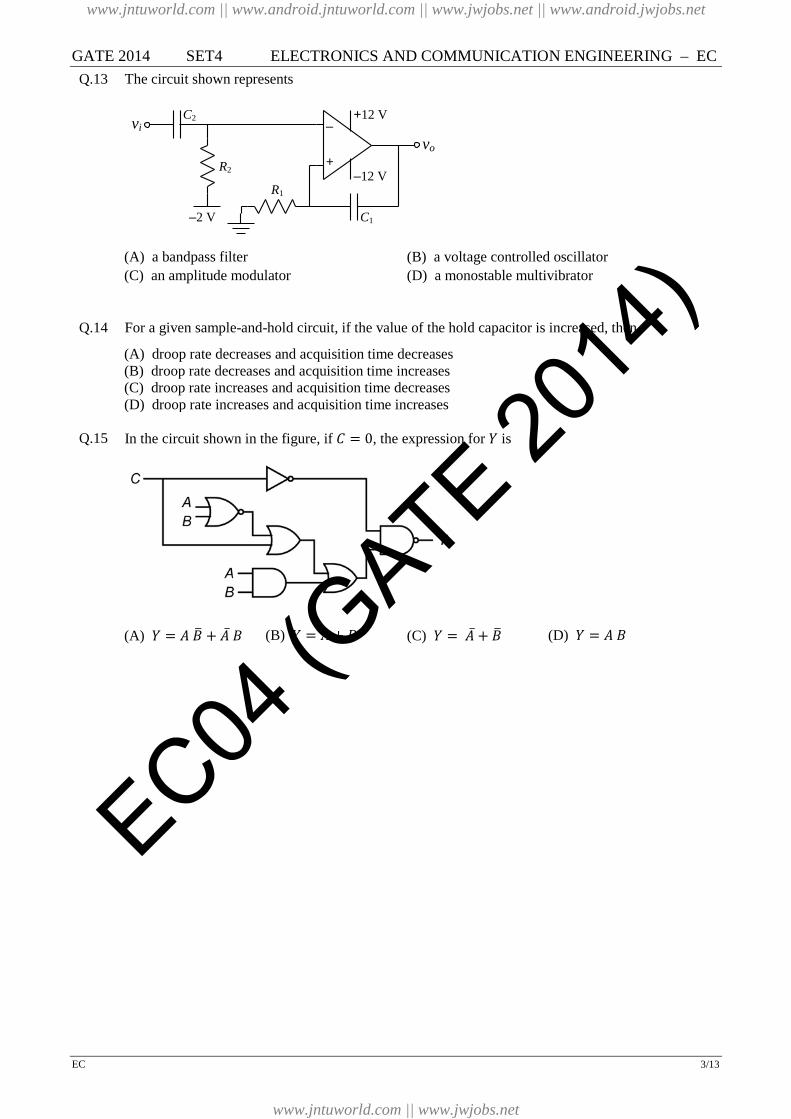
Q.13 The circuit shown represents
vi
–12 V
vo R2
C2
C1
R1
–
+
+12 V
–2 V
(A) a bandpass filter (B) a voltage controlled oscillator (C) an amplitude modulator (D) a monostable multivibrator
Q.14 For a given sample-and-hold circuit, if the value of the hold capacitor is increased, then
(A) droop rate decreases and acquisition time decreases (B) droop rate decreases and acquisition time increases (C) droop rate increases and acquisition time decreases (D) droop rate increases and acquisition time increases
Q.15 In the circuit shown in the figure, if 𝐶𝐶 = 0, the expression for 𝑌𝑌 is
(A) 𝑌𝑌 = 𝐴𝐴 𝐵𝐵 + 𝐴 𝐵𝐵 (B) 𝑌𝑌 = 𝐴𝐴 + 𝐵𝐵 (C) 𝑌𝑌 = 𝐴 + 𝐵𝐵 (D) 𝑌𝑌 = 𝐴𝐴 𝐵𝐵
EC04 (G
ATE 2014
)
www.jntuworld.com || www.android.jntuworld.com || www.jwjobs.net || www.android.jwjobs.net
www.jntuworld.com || www.jwjobs.net
GATE 2014 SET4 ELECTRONICS AND COMMUNICATION ENGINEERING – EC
EC 4/13
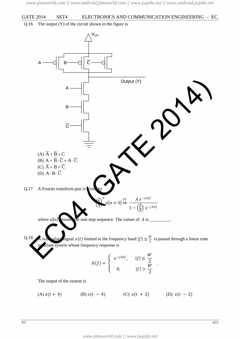
Q.16 The output (Y) of the circuit shown in the figure is
(A) CBA ++ (B) CACBA ⋅+⋅+ (C) CBA ++ (D) CBA ⋅⋅
Q.17 A Fourier transform pair is given by
23𝑛𝑛𝑢𝑢[𝑛𝑛 + 3]
𝐹𝐹𝐹𝐹⇔
𝐴𝐴 𝑒𝑒−𝑗𝑗6𝜋𝜋𝑓𝑓
1 − 23 𝑒𝑒−𝑗𝑗2𝜋𝜋𝑓𝑓
where 𝑢𝑢[𝑛𝑛] denotes the unit step sequence. The values of 𝐴𝐴 is _________.
Q.18 A real-valued signal 𝑥𝑥(𝑡𝑡) limited to the frequency band |𝑓𝑓| ≤ 𝑊𝑊
2 is passed through a linear time
invariant system whose frequency response is
𝐻𝐻(𝑓𝑓) = 𝑒𝑒−𝑗𝑗4𝜋𝜋𝑓𝑓 , |𝑓𝑓| ≤
𝑊𝑊2
0, |𝑓𝑓| > 𝑊𝑊2
.
The output of the system is
(A) 𝑥𝑥(𝑡𝑡 + 4) (B) 𝑥𝑥(𝑡𝑡 − 4) (C) 𝑥𝑥(𝑡𝑡 + 2) (D) 𝑥𝑥(𝑡𝑡 − 2)
A B C
A
B
C
Output (Y)
VDD
EC04 (G
ATE 2014
)
www.jntuworld.com || www.android.jntuworld.com || www.jwjobs.net || www.android.jwjobs.net
www.jntuworld.com || www.jwjobs.net

GATE 2014 SET4 ELECTRONICS AND COMMUNICATION ENGINEERING – EC
EC 5/13
Q.19 The sequence 𝑥𝑥[𝑛𝑛] = 0.5𝑛𝑛 𝑢𝑢[𝑛𝑛] , where 𝑢𝑢[𝑛𝑛] is the unit step sequence, is convolved with itself to obtain 𝑦𝑦[𝑛𝑛]. Then ∑ 𝑦𝑦[𝑛𝑛] + ∞
𝑛𝑛= − ∞ is _______.
Q.20 In a Bode magnitude plot, which one of the following slopes would be exhibited at high
frequencies by a 4th order all-pole system?
(A) – 80 dB/decade (B) – 40 dB/decade (C) +40 dB/decade (D) +80 dB/decade Q.21 For the second order closed-loop system shown in the figure, the natural frequency (in rad/s) is
(A) 16 (B) 4 (C) 2 (D) 1 Q.22 If calls arrive at a telephone exchange such that the time of arrival of any call is independent of the
time of arrival of earlier or future calls, the probability distribution function of the total number of calls in a fixed time interval will be
(A) Poisson (B) Gaussian (C) Exponential (D) Gamma Q.23 In a double side-band (DSB) full carrier AM transmission system, if the modulation index is
doubled, then the ratio of total sideband power to the carrier power increases by a factor of ______.
Q.24 For an antenna radiating in free space, the electric field at a distance of 1 km is found to be 12
mV/m. Given that intrinsic impedance of the free space is 120π Ω , the magnitude of average power density due to this antenna at a distance of 2 km from the antenna (in nW/m2 ) is ____.
Q.25 Match column A with column B.
Column A Column B 1. Point electromagnetic source P. Highly directional 2. Dish antenna Q. End fire 3. Yagi-Uda antenna R. Isotropic
(A) 1 → 𝑃𝑃 2 → 𝑄𝑄 3 → 𝑅𝑅
(B) 1 → 𝑅𝑅 2 → 𝑃𝑃 3 → 𝑄𝑄
(C) 1 → 𝑄𝑄 2 → 𝑃𝑃 3 → 𝑅𝑅
(D) 1 → 𝑅𝑅 2 → 𝑄𝑄 3 → 𝑃𝑃
U(s) Y(s) 4
s(s+4) - +
EC04 (G
ATE 2014
)
www.jntuworld.com || www.android.jntuworld.com || www.jwjobs.net || www.android.jwjobs.net
www.jntuworld.com || www.jwjobs.net

GATE 2014 SET4 ELECTRONICS AND COMMUNICATION ENGINEERING – EC
EC 6/13
Q. 26 – Q. 55 carry two marks each.
Q.26 With initial values 𝑦𝑦(0) = 𝑦𝑦′(0) = 1, the solution of the differential equation
𝑑𝑑2𝑦𝑦𝑑𝑑𝑥𝑥2 + 4
𝑑𝑑𝑦𝑦𝑑𝑑𝑥𝑥
+ 4𝑦𝑦 = 0
at 𝑥𝑥 = 1 is _____.
Q.27 Parcels from sender S to receiver R pass sequentially through two post-offices. Each post-office has
a probability 15 of losing an incoming parcel, independently of all other parcels. Given that a parcel
is lost, the probability that it was lost by the second post-office is_________.
Q.28 The unilateral Laplace transform of 𝑓𝑓(𝑡𝑡) is 1
𝑠𝑠2+𝑠𝑠+1. Which one of the following is the unilateral
Laplace transform of 𝑔𝑔(𝑡𝑡) = 𝑡𝑡 ∙ 𝑓𝑓(𝑡𝑡)?
(A) − 𝑠𝑠(𝑠𝑠2+𝑠𝑠+1)2 (B) −(2𝑠𝑠+1)
(𝑠𝑠2+𝑠𝑠+1)2
(C) 𝑠𝑠(𝑠𝑠2+𝑠𝑠+1)2 (D) 2𝑠𝑠+1
(𝑠𝑠2+𝑠𝑠+1)2
Q.29 For a right angled triangle, if the sum of the lengths of the hypotenuse and a side is kept constant, in
order to have maximum area of the triangle, the angle between the hypotenuse and the side is
(A) 12o (B) 36o (C) 60o (D) 45o Q.30 The steady state output of the circuit shown in the figure is given by
𝑦𝑦(𝑡𝑡) = 𝐴𝐴(𝜔𝜔) sin(𝜔𝜔𝑡𝑡 + 𝜙𝜙(𝜔𝜔)). If the amplitude | 𝐴𝐴(𝜔𝜔)| = 0.25 , then the frequency 𝜔𝜔 is
(A) 1√3 𝑅𝑅 𝐶𝐶
(B) 2√3 𝑅𝑅 𝐶𝐶
(C) 1𝑅𝑅 𝐶𝐶
(D) 2𝑅𝑅 𝐶𝐶
Q.31 In the circuit shown in the figure, the value of v0(t) (in Volts) for t → ∞ is ______.
5 Ω
5 Ω
2 H
10 u(t) A
xi
+
-
+- v (t)o
2ix
R
C
C
C
sin(ωt)
y(t)
EC04 (G
ATE 2014
)
www.jntuworld.com || www.android.jntuworld.com || www.jwjobs.net || www.android.jwjobs.net
www.jntuworld.com || www.jwjobs.net

GATE 2014 SET4 ELECTRONICS AND COMMUNICATION ENGINEERING – EC
EC 7/13
Q.32 The equivalent resistance in the infinite ladder network shown in the figure, is Re.
The value of Re/R is ________
Q.33 For the two-port network shown in the figure, the impedance (Z) matrix (in Ω) is
(A) 6 2442 9 (B) 9 8
8 24 (C) 9 66 24 (D) 42 6
6 60 Q.34 Consider a silicon sample doped with ND = 1×10¹⁵/cm3 donor atoms. Assume that the intrinsic
carrier concentration ni = 1.5×10¹⁰/cm3. If the sample is additionally doped with NA = 1×10¹⁸/cm3 acceptor atoms, the approximate number of electrons/cm3 in the sample, at T=300 K, will be ______.
Q.35 Consider two BJTs biased at the same collector current with area A1 = 0.2 µm × 0.2 µm and A2 = 300 µm × 300 µm. Assuming that all other device parameters are identical, kT/q = 26 mV, the intrinsic carrier concentration is 1 × 1010 cm-3, and q = 1.6 × 10⁻¹⁹ C, the difference between the base-emitter voltages (in mV) of the two BJTs (i.e., VBE1 – VBE2) is _____. EC04
(GATE 20
14)
www.jntuworld.com || www.android.jntuworld.com || www.jwjobs.net || www.android.jwjobs.net
www.jntuworld.com || www.jwjobs.net
GATE 2014 SET4 ELECTRONICS AND COMMUNICATION ENGINEERING – EC
EC 8/13
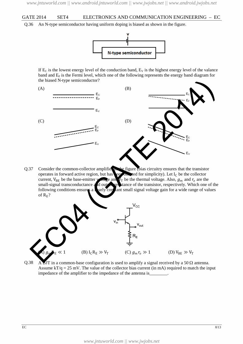
Q.36 An N-type semiconductor having uniform doping is biased as shown in the figure.
If EC is the lowest energy level of the conduction band, EV is the highest energy level of the valance band and EF is the Fermi level, which one of the following represents the energy band diagram for the biased N-type semiconductor?
(A) EC
EV
EF
(B) EC
EV
EF
(C) EC
EV
EF
(D)
EC
EV
EF
Q.37 Consider the common-collector amplifier in the figure (bias circuitry ensures that the transistor
operates in forward active region, but has been omitted for simplicity). Let IC be the collector current, VBE be the base-emitter voltage and VT be the thermal voltage. Also, 𝑔𝑔𝑚𝑚 and 𝑟𝑟𝑜𝑜 are the small-signal transconductance and output resistance of the transistor, respectively. Which one of the following conditions ensures a nearly constant small signal voltage gain for a wide range of values of RE?
(A) 𝑔𝑔𝑚𝑚RE ≪ 1 (B) ICRE ≫ VT (C) 𝑔𝑔𝑚𝑚𝑟𝑟𝑜𝑜 ≫ 1 (D) VBE ≫ VT
Q.38 A BJT in a common-base configuration is used to amplify a signal received by a 50 Ω antenna.
Assume kT/q = 25 mV. The value of the collector bias current (in mA) required to match the input impedance of the amplifier to the impedance of the antenna is________.
EC04 (G
ATE 2014
)
www.jntuworld.com || www.android.jntuworld.com || www.jwjobs.net || www.android.jwjobs.net
www.jntuworld.com || www.jwjobs.net

GATE 2014 SET4 ELECTRONICS AND COMMUNICATION ENGINEERING – EC
EC 9/13
Q.39 For the common collector amplifier shown in the figure, the BJT has high β, negligible VCE(sat), and VBE = 0.7 V. The maximum undistorted peak-to-peak output voltage vo (in Volts) is _______.
vi
vo RE
1 kΩ
VCC = +12 V
R1
5 kΩ
•
R2
10 kΩ
1 µF
1 µF
Q.40 An 8-to-1 multiplexer is used to implement a logical function 𝑌𝑌 as shown in the figure. The output
𝑌𝑌 is given by
(A) 𝑌𝑌 = 𝐴𝐴 𝐵𝐵 𝐶𝐶 + 𝐴𝐴 𝐶𝐶 𝐷𝐷 (B) 𝑌𝑌 = 𝐴 𝐵𝐵 𝐶𝐶 + 𝐴𝐴 𝐵𝐵 𝐷𝐷 (C) 𝑌𝑌 = 𝐴𝐴 𝐵𝐵 𝐶𝐶 + 𝐴 𝐶𝐶 𝐷𝐷 (D) 𝑌𝑌 = 𝐴 𝐵𝐵 𝐷𝐷 + 𝐴𝐴 𝐵𝐵 𝐶𝐶
Q.41 A 16-bit ripple carry adder is realized using 16 identical full adders (FA) as shown in the figure.
The carry-propagation delay of each FA is 12 ns and the sum-propagation delay of each FA is 15 ns. The worst case delay (in ns) of this 16-bit adder will be __________.
FA0
S0
C0
A0 B0
FA1
S1
A1 B1
C1 FA14
S14
C14
A14 B14
FA15
S15
A15 B15
C15
Q.42 An 8085 microprocessor executes “STA 1234H” with starting address location 1FFEH (STA copies
the contents of the Accumulator to the 16-bit address location). While the instruction is fetched and executed, the sequence of values written at the address pins A15 − A8 is
(A) 1FH, 1FH, 20H, 12H (B) 1FH, FEH, 1FH, FFH, 12H (C) 1FH, 1FH, 12H, 12H (D) 1FH, 1FH, 12H, 20H, 12H
EC04 (G
ATE 2014
)
www.jntuworld.com || www.android.jntuworld.com || www.jwjobs.net || www.android.jwjobs.net
www.jntuworld.com || www.jwjobs.net

GATE 2014 SET4 ELECTRONICS AND COMMUNICATION ENGINEERING – EC
EC 10/13
Q.43 A stable linear time invariant (LTI) system has a transfer function 𝐻𝐻(𝑠𝑠) = 1𝑠𝑠2+𝑠𝑠−6
. To make this system causal it needs to be cascaded with another LTI system having a transfer function 𝐻𝐻1(𝑠𝑠). A correct choice for 𝐻𝐻1(𝑠𝑠) among the following options is
(A) 𝑠𝑠 + 3 (B) 𝑠𝑠 − 2 (C) 𝑠𝑠 − 6 (D) 𝑠𝑠 + 1
Q.44 A causal LTI system has zero initial conditions and impulse response ℎ(𝑡𝑡). Its input 𝑥𝑥(𝑡𝑡) and
output 𝑦𝑦(𝑡𝑡) are related through the linear constant-coefficient differential equation
𝑑𝑑2𝑦𝑦(𝑡𝑡)𝑑𝑑𝑡𝑡2 + 𝛼𝛼
𝑑𝑑𝑦𝑦(𝑡𝑡)𝑑𝑑𝑡𝑡
+ 𝛼𝛼2𝑦𝑦(𝑡𝑡) = 𝑥𝑥(𝑡𝑡). Let another signal 𝑔𝑔(𝑡𝑡) be defined as
𝑔𝑔(𝑡𝑡) = 𝛼𝛼2 ℎ(𝜏𝜏)𝑑𝑑𝜏𝜏𝑡𝑡
0
+𝑑𝑑ℎ(𝑡𝑡)𝑑𝑑𝑡𝑡
+ 𝛼𝛼ℎ(𝑡𝑡).
If 𝐺𝐺(𝑠𝑠) is the Laplace transform of 𝑔𝑔(𝑡𝑡), then the number of poles of 𝐺𝐺(𝑠𝑠) is _____.
Q.45 The 𝑁𝑁-point DFT 𝑋𝑋 of a sequence 𝑥𝑥[𝑛𝑛], 0 ≤ 𝑛𝑛 ≤ 𝑁𝑁 − 1 is given by
𝑋𝑋[𝑘𝑘] = 1√𝑁𝑁
𝑥𝑥[𝑛𝑛]𝑒𝑒−𝑗𝑗 2𝜋𝜋𝑁𝑁 𝑛𝑛𝑘𝑘 , 0 ≤ 𝑘𝑘 ≤ 𝑁𝑁 − 1.𝑁𝑁−1
𝑛𝑛=0
Denote this relation as 𝑋𝑋 = 𝐷𝐷𝐹𝐹𝐹𝐹(𝑥𝑥). For 𝑁𝑁 = 4, which one of the following sequences satisfies 𝐷𝐷𝐹𝐹𝐹𝐹(𝐷𝐷𝐹𝐹𝐹𝐹(𝑥𝑥)) = 𝑥𝑥 ?
(A) 𝑥𝑥 = [1 2 3 4] (B) 𝑥𝑥 = [1 2 3 2] (C) 𝑥𝑥 = [1 3 2 2] (D) 𝑥𝑥 = [1 2 2 3]
Q.46 The state transition matrix 𝜙𝜙(t) of a system 𝑥1
𝑥2 = 0 1
0 0 𝑥𝑥1𝑥𝑥2 is
(A) 𝑡𝑡 11 0
(B) 1 0
𝑡𝑡 1
(C) 0 11 𝑡𝑡
(D) 1 𝑡𝑡
0 1
Q.47
Consider a transfer function 𝐺𝐺𝑝𝑝(𝑠𝑠) = 𝑝𝑝𝑠𝑠2+3𝑝𝑝𝑠𝑠−2
𝑠𝑠2+(3+𝑝𝑝)𝑠𝑠+(2−𝑝𝑝) with 𝑝𝑝 a positive real parameter. The
maximum value of 𝑝𝑝 until which 𝐺𝐺𝑝𝑝 remains stable is ________.
EC04
(GATE 20
14)
www.jntuworld.com || www.android.jntuworld.com || www.jwjobs.net || www.android.jwjobs.net
www.jntuworld.com || www.jwjobs.net

GATE 2014 SET4 ELECTRONICS AND COMMUNICATION ENGINEERING – EC
EC 11/13
Q.48 The characteristic equation of a unity negative feedback system is 1 + 𝐾𝐾𝐺𝐺(𝑠𝑠) = 0. The open loop transfer function 𝐺𝐺(𝑠𝑠) has one pole at 0 and two poles at -1. The root locus of the system for varying K is shown in the figure.
O
A
ξ=0.5
σ
ω
(0,0)−1 −1/3
j
The constant damping ratio line, for ξ=0.5, intersects the root locus at point A. The distance from the origin to point A is given as 0.5. The value of 𝐾𝐾 at point A is ________ .
Q.49 Consider a communication scheme where the binary valued signal X satisfies 𝑃𝑃𝑋𝑋 = +1 = 0.75
and 𝑃𝑃𝑋𝑋 = −1 = 0.25. The received signal Y = X + Z, where Z is a Gaussian random variable with zero mean and variance 𝜎𝜎2. The received signal Y is fed to the threshold detector. The output of the threshold detector 𝑋𝑋 is:
𝑋𝑋 = +1, 𝑌𝑌 > 𝜏𝜏−1, 𝑌𝑌 ≤ 𝜏𝜏.
To achieve a minimum probability of error 𝑃𝑃𝑋𝑋 ≠ 𝑋𝑋, the threshold τ should be
(A) strictly positive (B) zero (C) strictly negative (D) strictly positive, zero, or strictly negative depending on the nonzero value of 𝜎𝜎2
EC04 (G
ATE 2014
)
www.jntuworld.com || www.android.jntuworld.com || www.jwjobs.net || www.android.jwjobs.net
www.jntuworld.com || www.jwjobs.net
GATE 2014 SET4 ELECTRONICS AND COMMUNICATION ENGINEERING – EC
EC 12/13
Q.50 Consider the Z-channel given in the figure. The input is 0 or 1 with equal probability.
If the output is 0, the probability that the input is also 0 equals ______________
Q.51 An M-level PSK modulation scheme is used to transmit independent binary digits over a band-pass
channel with bandwidth 100 kHz. The bit rate is 200 kbps and the system characteristic is a raised-cosine spectrum with 100% excess bandwidth. The minimum value of M is ________.
Q.52 Consider a discrete-time channel 𝑌𝑌 = 𝑋𝑋 + 𝑍𝑍, where the additive noise 𝑍𝑍 is signal-dependent.
In particular, given the transmitted symbol 𝑋𝑋 ∈ −𝑎𝑎, +𝑎𝑎 at any instant, the noise sample 𝑍𝑍 is chosen independently from a Gaussian distribution with mean 𝛽𝛽𝑋𝑋 and unit variance. Assume a threshold detector with zero threshold at the receiver. When 𝛽𝛽 = 0, the BER was found to be 𝑄𝑄(𝑎𝑎) = 1 × 10⁻⁸. (𝑄𝑄(𝑣𝑣) = 1
√2𝜋𝜋 ∫ 𝑒𝑒−𝑢𝑢2 2⁄∞𝑣𝑣 𝑑𝑑𝑢𝑢, and for 𝑣𝑣 > 1, use 𝑄𝑄(𝑣𝑣) ≈ 𝑒𝑒−𝑣𝑣2 2⁄ )
When 𝛽𝛽 = −0.3, the BER is closest to
(A) 10−7 (B) 10−6 (C) 10−4 (D) 10−2
Q.53 The electric field (assumed to be one-dimensional) between two points A and B is shown. Let 𝜓𝜓𝐴𝐴
and 𝜓𝜓𝐵𝐵 be the electrostatic potentials at A and B, respectively. The value of 𝜓𝜓𝐵𝐵–𝜓𝜓𝐴𝐴 in Volts is ________.
Q.54 Given ˆ ˆ ˆx y zF za xa ya= + +
. If S represents the portion of the sphere 2 2 2 1x y z+ + = for 0z ≥ ,
then ∫ ∇ × 𝐹𝐹 ∙𝑠𝑠 𝑑𝑑𝑠𝑠 is______________.
INPUT
0
1
0
1
OUTPUT
1.0
0.25
0.75
EC04 (G
ATE 2014
)
www.jntuworld.com || www.android.jntuworld.com || www.jwjobs.net || www.android.jwjobs.net
www.jntuworld.com || www.jwjobs.net
GATE 2014 SET4 ELECTRONICS AND COMMUNICATION ENGINEERING – EC
EC 13/13
Q.55 If 𝐸𝐸 = −(2𝑦𝑦3 − 3𝑦𝑦𝑧𝑧2)𝑥𝑥 − (6𝑥𝑥𝑦𝑦2 − 3𝑥𝑥𝑧𝑧2)𝑦𝑦 + (6𝑥𝑥𝑦𝑦𝑧𝑧)𝑧 is the electric field in a source free region, a valid expression for the electrostatic potential is
(A) 𝑥𝑥𝑦𝑦3 − 𝑦𝑦𝑧𝑧2 (B) 2𝑥𝑥𝑦𝑦3 − 𝑥𝑥𝑦𝑦𝑧𝑧2 (C) 𝑦𝑦3 + 𝑥𝑥𝑦𝑦𝑧𝑧2 (D) 2𝑥𝑥𝑦𝑦3 − 3𝑥𝑥𝑦𝑦𝑧𝑧2
END OF THE QUESTION PAPER
EC04 (G
ATE 2014
)
www.jntuworld.com || www.android.jntuworld.com || www.jwjobs.net || www.android.jwjobs.net
www.jntuworld.com || www.jwjobs.net