Gate Array S1L60000 Series Design Guide - Epson · 2008-08-25 · Chapter 1: Overview GATE ARRAY...
230
MF1246-04 DESIGN GUIDE GATE ARRAY S1L60000 Series
Transcript of Gate Array S1L60000 Series Design Guide - Epson · 2008-08-25 · Chapter 1: Overview GATE ARRAY...
MF1246-04
DESIGN GUIDE
GATE ARRAY
S1L60000 Series

NOTICE
No part of this material may be reproduced or duplicated in any from or by any means without thewritten permission of EPSON. EPSON reserves the right to make changes to this material withoutnotice. EPSON does not assume any liability of any kind arising out of any inaccuracies containedin this material or due to its application or use in any product or circuit and, further, there is norepresentation that this material is applicable to products requiring high level reliability, such as,medical products. Moreover, no license to any intellectual property rights is granted by implicationor otherwise, and there is no representation or warranty that anything made in accordance withthis marerial will be free from any patent or copyright infringement of a third party. This material orportions there of may contain techology or the subject relating to strategic products under thecontrol of the Forign Exchange and Foreign Trade Law of Japan and may require an exportlicense from the Ministry of international Trade and Industry or other approval from anothergovernment agency.
MS-DOS and Windows are registered trademarks of Microsoft Corporation, U.S.A.PC-DOS, PC/AT. VGA. EGA and IBM are registered trademarks of International Business Machines Corporation, U.S.A.All other product names mentioned herein are trademarks and/or registered trademarks of their respective owners.
©SEIKO EPSON CORPORATION 2003, All rights reserved.
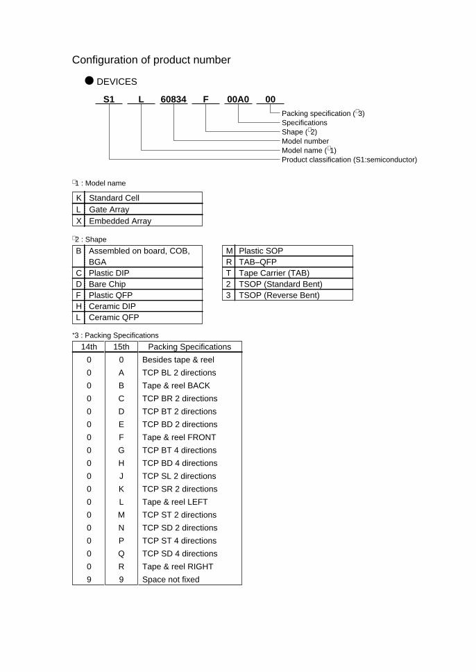
Configuration of product number
DEVICES
S1 L 60834 F 00A0Packing specification (∗ 3)SpecificationsShape (∗ 2)Model numberModel name (∗ 1)Product classification (S1:semiconductor)
00
∗ 1 : Model name
∗ 2 : Shape
K Standard CellL Gate ArrayX Embedded Array
B Assembled on board, COB,BGA
C Plastic DIPD Bare ChipF Plastic QFPH Ceramic DIPL Ceramic QFP
M Plastic SOPR TAB–QFPT Tape Carrier (TAB)2 TSOP (Standard Bent)3 TSOP (Reverse Bent)
*3 : Packing Specifications
14th 15th Packing Specifications
0 0 Besides tape & reel
0 A TCP BL 2 directions
0 B Tape & reel BACK
0 C TCP BR 2 directions
0 D TCP BT 2 directions
0 E TCP BD 2 directions
0 F Tape & reel FRONT
0 G TCP BT 4 directions
0 H TCP BD 4 directions
0 J TCP SL 2 directions
0 K TCP SR 2 directions
0 L Tape & reel LEFT
0 M TCP ST 2 directions
0 N TCP SD 2 directions
0 P TCP ST 4 directions
0 Q TCP SD 4 directions
0 R Tape & reel RIGHT
9 9 Space not fixed

Contents
S1L60000 Series Table of Contents
Chapter 1 Overview.............................................................................................. 11.1 Features....................................................................................................................11.2 Master Structure .......................................................................................................21.3 Electrical Characteristics and Specifications ............................................................31.4 Overview of Gate Array Development Flow............................................................11
Chapter 2 Estimating Gate Density and Selecting the Master ....................... 132.1 Dividing Up Logic Between Chips...........................................................................132.2 Determining Gate Size............................................................................................132.3 Estimating the Number of Input/Output Pins ..........................................................132.4 Selecting the Master ...............................................................................................142.5 Estimating the BCs That Can Be Used in Circuits Which Include RAM .................14
Chapter 3 Cautions and Notes Regarding Circuit Design.............................. 153.1 Inserting I/O Buffers................................................................................................153.2 The Use of Differentiating Circuits is Forbidden .....................................................153.3 Wired Logic is Forbidden........................................................................................153.4 Hazard Countermeasures.......................................................................................163.5 Limitations on Logic Gate Output Load ..................................................................163.6 Bus Circuits.............................................................................................................163.7 Bus Hold Circuits ....................................................................................................183.8 Schematic Capture Guidelines ...............................................................................183.9 Clock Tree Synthesis..............................................................................................193.10 ATPG (Auto Test Pattern Generation)....................................................................273.11 Restrictions and Constraints on VHDL/Verilog-HDL Netlist....................................36
3.11.1 Common Restrictions and Constraints ...........................................................................363.11.2 Restrictions and Constraints for Verilog Netlist ..............................................................363.11.3 Restrictions and Constraints on VHDL Netlist ................................................................37
Chapter 4 Input/Out Cells Buffers and Their Use............................................ 384.1 Types of Input/Output Buffer in the S1L60000 Series ............................................38
4.1.1 Selecting I/O Buffer ........................................................................................................384.2 I/O Buffer Configurations with a Single Power Supply............................................40
4.2.1 I/O Buffer Configurations with a Single Power Supply ...................................................404.2.1.1 Input Buffer Configurations with a Single Power Supply .......................................404.2.1.2 Output Buffer Configurations with a Single Power Supply ....................................404.2.1.3 Bi-directional Buffer Configurations with a Single Power Supply ..........................43
4.3 Oscillation Circuit ....................................................................................................474.3.1 Oscillation Circuit Configurations....................................................................................474.3.2 Oscillation Circuit Considerations...................................................................................47
4.4 Gated I/O Cells .......................................................................................................484.4.1 Overview of Gated Cells.................................................................................................484.4.2 Feature of Gated I/O Cell ...............................................................................................484.4.3 Notes on Using Gated Cell .............................................................................................49
4.5 Fail Safe Cell ..........................................................................................................524.5.1 Overview of Fail Safe Cell ..............................................................................................524.5.2 Feature of Fail Safe Cell .................................................................................................524.5.3 Notes on Using Fail Safe Cell.........................................................................................52
Chapter 5 RAM.................................................................................................... 545.1 Features..................................................................................................................54
GATE ARRAY S1L60000 SERIES EPSON iDESIGN GUIDE

Contents
5.2 RAM Configuration and Simulation Model Selection ..............................................545.3 RAM Size................................................................................................................555.4 Investigating RAM Placement on Master Slice.......................................................565.5 Explanation of Functions ........................................................................................575.6 Delay Parameters ...................................................................................................605.7 Timing Charts .........................................................................................................925.8 RAM Test Method...................................................................................................945.9 Estimating RAM Current Consumption...................................................................945.10 RAM Symbols and How They Are Used.................................................................95
Chapter 6 Circuit Design Taking Testability Into Account............................. 966.1 Considerations Regarding Circuit Initialization .......................................................966.2 Considerations Regarding Compressing the Test Patterns....................................966.3 Test Circuit Which Simplifies AC and DC Testing ..................................................97
6.3.1 Test Circuit Structure ..................................................................................................... 976.4 RAM Test Circuit...................................................................................................104
6.4.1 RAM Test Patterns....................................................................................................... 1046.5 Function Cell Test Circuits....................................................................................107
6.5.1 Test Circuit Structures.................................................................................................. 1076.5.2 Test Patterns................................................................................................................ 1076.5.3 Test Circuit Data .......................................................................................................... 108
Chapter 7 Propagation Delay and Timing...................................................... 1107.1 Notes on the relationship between Ta and Tj .......................................................1107.2 Simple Delay Models ............................................................................................1107.3 Load Due to Input Capacitance (Load A) .............................................................1127.4 Load Due to Interconnect Capacitance (Load B)..................................................1137.5 Propagation Delay Calculations............................................................................1137.6 Calculating Output Buffer Delay ...........................................................................1157.7 Sequential Buffer Setup/Hold Time ......................................................................1157.8 Cells with Increased Speed ..................................................................................1187.9 Chip Internal Skew................................................................................................118
Chapter 8 Test Pattern Generation................................................................. 1198.1 Testability Considerations.....................................................................................1198.2 Waveform Types...................................................................................................1198.3 Constraints on the Types of Test Patterns ...........................................................120
8.3.1 Test Period................................................................................................................... 1208.3.2 Input Delay ................................................................................................................... 1208.3.3 Pulse Width .................................................................................................................. 1218.3.4 Input Waveform Format ............................................................................................... 1218.3.5 Strobe........................................................................................................................... 121
8.4 Notes Regarding DC Testing................................................................................1218.5 Notes Regarding the Use of Oscillation Circuits...................................................1248.6 Regarding AC Testing ..........................................................................................125
8.6.1 Constraints Regarding Measurement Events .............................................................. 1258.6.2 Constraints on the Measurement Locations for AC Testing......................................... 1258.6.3 Constraints Regarding the Path Delay Which is Tested .............................................. 1258.6.4 Other Constraints ......................................................................................................... 125
8.7 Test Pattern Constraints for Bi-directional Pins ....................................................1268.8 Notes on Devices at High Impedance ..................................................................126
ii EPSON GATE ARRAY S1L60000 SERIES DESIGN GUIDE
Contents
Chapter 9 Estimating the Power Consumption ............................................ 1289.1 Calculating the Power Consumption.....................................................................1289.2 Constraints on Power Consumption .....................................................................131
Chapter 10 Pin Layout Considerations ............................................................ 13210.1 Estimating the Number of Power Supply Pins ......................................................13210.2 Number of Simultaneous Operations and Adding Power Supplies ......................13210.3 Cautions and Notes Regarding the Layout of pins ...............................................135
10.3.1 Fixed Power Supply Pins..............................................................................................13510.3.2 Cautions and Notes Regarding the Pin Layout ............................................................13510.3.3 Examples of Recommended Pin Connections .............................................................142
Chapter 11 Dual Power Supplies Guidelines................................................... 14411.1 The Method of Adapting to Dual Power Supplies .................................................14411.2 Power Supplies for Dual Power Operation ...........................................................14411.3 Turming ON/OFF Dual Power Supplies................................................................14511.4 I/O Buffers Compatible with Dual Power Supplies................................................145
11.4.1 I/O Buffers for the LVDD System..................................................................................14511.4.1.1 Input Buffers for the LVDD System .....................................................................14611.4.1.2 Output Buffers for the LVDD System...................................................................14711.4.1.3 Bi-directional Buffers for the LVDD System.........................................................150
11.4.2 I/O Buffers for the HVDD System .................................................................................15211.4.2.1 Input Buffers for the HVDD System.....................................................................15311.4.2.2 Output Buffers for the HVDD System..................................................................15411.4.2.3 Bi-directional Buffers for the HVDD System........................................................156
11.5 Delay Calculation for Dual Power Supplies ..........................................................15911.6 Cautions and Notes Regarding Power Consumption Calculations When
Using Dual Power Supplies ..................................................................................15911.7 Estimating the Number of Power Supply Pins When Using Dual Power
Supplies ................................................................................................................161
Chapter 12 RAM (Clock Synchronous Type) ................................................... 16312.1 Features................................................................................................................16312.2 Word/Bit Configurations and Cell Names of the RAM ..........................................16312.3 Number of Basic Cells for Synchronous RAM......................................................16412.4 Investigating RAM Placement on Master Slice.....................................................16512.5 Functional Description ..........................................................................................166
12.5.1 1-port RAM (Clock Synchronous Type)........................................................................16612.5.2 2-port RAM (Clock Synchronous Type)........................................................................167
12.6 Timing Charts .......................................................................................................17012.7 Delay Parameters .................................................................................................17212.8 Method for Testing the RAM.................................................................................18812.9 Estimating RAM Current Consumption.................................................................189
Appendix A1.Electrical Characteristica Data .................................................... 190A1.1 3.3V operation ......................................................................................................190A1.2 2.5V operation ......................................................................................................199A1.3 2.0V operation ......................................................................................................209A1.4 Estimated Wiring Load Table................................................................................219
Appendix A2.Release Note.................................................................................. 221
GATE ARRAY S1L60000 SERIES EPSON iiiDESIGN GUIDE
Contents
iv EPSON GATE ARRAY S1L60000 SERIES DESIGN GUIDE
Chapter 1: Overview
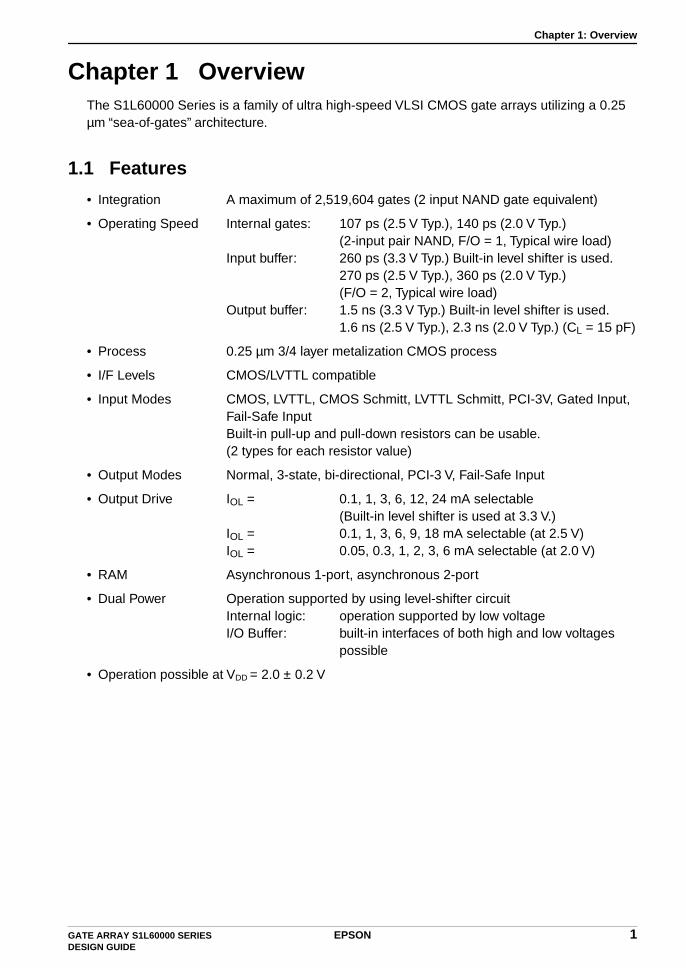
Chapter 1 OverviewThe S1L60000 Series is a family of ultra high-speed VLSI CMOS gate arrays utilizing a 0.25 µm “sea-of-gates” architecture.
1.1 Features
• Integration A maximum of 2,519,604 gates (2 input NAND gate equivalent)
• Operating Speed Internal gates: 107 ps (2.5 V Typ.), 140 ps (2.0 V Typ.)(2-input pair NAND, F/O = 1, Typical wire load)
Input buffer: 260 ps (3.3 V Typ.) Built-in level shifter is used.270 ps (2.5 V Typ.), 360 ps (2.0 V Typ.)(F/O = 2, Typical wire load)
Output buffer: 1.5 ns (3.3 V Typ.) Built-in level shifter is used.1.6 ns (2.5 V Typ.), 2.3 ns (2.0 V Typ.) (CL = 15 pF)
• Process 0.25 µm 3/4 layer metalization CMOS process
• I/F Levels CMOS/LVTTL compatible
• Input Modes CMOS, LVTTL, CMOS Schmitt, LVTTL Schmitt, PCI-3V, Gated Input,Fail-Safe InputBuilt-in pull-up and pull-down resistors can be usable.(2 types for each resistor value)
• Output Modes Normal, 3-state, bi-directional, PCI-3 V, Fail-Safe Input
• Output Drive IOL = 0.1, 1, 3, 6, 12, 24 mA selectable(Built-in level shifter is used at 3.3 V.)
IOL = 0.1, 1, 3, 6, 9, 18 mA selectable (at 2.5 V)IOL = 0.05, 0.3, 1, 2, 3, 6 mA selectable (at 2.0 V)
• RAM Asynchronous 1-port, asynchronous 2-port
• Dual Power Operation supported by using level-shifter circuitInternal logic: operation supported by low voltageI/O Buffer: built-in interfaces of both high and low voltages
possible
• Operation possible at VDD = 2.0 ± 0.2 V
GATE ARRAY S1L60000 SERIES EPSON 1DESIGN GUIDE

Chapter 1: Overview
1.2 Master Structure
The S1L60000 Series comprises 10 types of masters, from which the customer is able to select the master most suitable.
NOTE: *1: This is the value when there are no cells, such as RAM cells. The cell use effciency is, dependent not only on the scope of the circuits, but also on the number of signals, the number of branches per signal, and operating frequency etc.; thus, use the values in this table only as an estimate.
Table 1-1 Overview
MasterTotal BC
(Raw Gates)
Number of Pads
BC Columns and Rows Cell utilization ratio (U)*1
Number of Columns
(X)
Number of Rows
(Y)3-layer metal 4-layer metal
S1L60093/60094 99220 112 605 164 60 70
S1L60173/60174 171720 148 795 216 60 70
S1L60283/60284 284394 188 1023 278 50 65
S1L60403/60404 400290 224 1213 330 50 65
S1L60593/60594 595362 272 1481 402 50 65
S1L60833/60834 831572 284 1747 476 40 50
S1L61233/61234 1234820 344 2129 580 40 50
S1L61583/61584 1587754 388 2413 658 40 50
S1L61903/61904 1902960 424 2643 720 40 50
S1L62513/62514 2519604 488 3043 828 40 50
2 EPSON GATE ARRAY S1L60000 SERIES DESIGN GUIDE

Chapter 1: Overview
1.3 Electrical Characteristics and Specifications
*1: Possibles to use from -0.3 V to 4.0 V of N channel open drain bi-directional buffers, input buffer and Fail Safe cells.
*1: Possibles to use from -0.3 V to 4.0 V of N channel open drain bi-directional buffers, input buffer and Fail Safe cells.
*2: Possibles to use for 24 mA of output buffer.
*3: HVDD ≥ LVDD
Table 1-2 Absolute Maximum Ratings (For Single Power Supplies)(VSS = 0 V)
Item Symbol Limits Unit
Power Supply Voltage VDD -0.3 to 3.0 V
Input Voltage VI -0.3 to VDD + 0.5*1 V
Output Voltage VO -0.3 to VDD + 0.5*1 V
Output Current/Pin IOUT ± 30 mA
Storage Temperature TSTG -65 to 150 °C
Table 1-3 Absolute Maximum Ratings (For Dual Power Supplies)(VSS = 0 V)
Item Symbol Limits Unit
Power Supply VoltageHVDD*3 -0.3 to 4.0 V
LVDD*3 -0.3 to 3.0 V
Input VoltageHVI -0.3 to HVDD + 0.5*1 V
LVI -0.3 to LVDD + 0.5*1 V
Output VoltageHVO -0.3 to HVDD + 0.5*1 V
LVO -0.3 to LVDD + 0.5*1 V
Output Current/Pin IOUT ± 30 ( ± 50*2) mA
Storage Temperature TSTG -65 to 150 °C
GATE ARRAY S1L60000 SERIES EPSON 3DESIGN GUIDE

Chapter 1: Overview
*1: Possibles to use 3.6 V of N channel open drain bi-directional buffers, input buffers, and Fail Safe cells.
*2: The ambient temperature range is recommended for Tj = 0 to 85°C.
*3: The ambient temperature range is recommended for Tj = -40 to 125°C.
*4: These timing parameters indicate a 10% to 90% VDD change time.
Table 1-4-1 Recommended Operating Conditions (For Single Power Supplies)
Item Symbol Min. Typ. Max. Unit
Power Supply Voltage VDD 2.30 2.50 2.70 V
Input Voltage VI VSS — VDD*1 V
Ambient Temperature Ta0
-402525
70*2
85*3°C
Normal Input Rising Time*4 tri — — 50 ns
Normal Input Falling Time*4 tfa — — 50 ns
Schmitt Input Rising Time*4 tri — — 5 ms
Schmitt Input Falling Time*4 tfa — — 5 ms
Table 1-4-2 Recommended Operating Conditions (For Single Power Supplies)
Item Symbol Min. Typ. Max. Unit
Power Supply Voltage VDD 1.80 2.00 2.20 V
Input Voltage VI VSS — VDD*1 V
Ambient Temperature Ta0
-402525
70*2
85*3°C
Normal Input Rising Time*4 tri — — 100 ns
Normal Input Falling Time*4 tfa — — 100 ns
Schmitt Input Rising Time*4 tri — — 10 ms
Schmitt Input Falling Time*4 tfa — — 10 ms
4 EPSON GATE ARRAY S1L60000 SERIES DESIGN GUIDE

Chapter 1: Overview
*1: Possibles to use 3.6 V of N channel open drain bi-directional buffers, input buffers, and Fail Safe cells.
*2: The ambient temperature range is recommended for Tj = 0 to 85°C.
*3: The ambient temperature range is recommended for Tj = -40 to 125°C.
*4: These timing parameters indicate a 10% to 90% VDD change time.
*1: Possibles to use 3.6 V of N channel open drain bi-directional buffers, input buffers, and Fail Safe cells.
*2: The ambient temperature range is recommended for Tj = 0 to 85°C.
*3: The ambient temperature range is recommended for Tj = -40 to 125°C.
*4: These timing parameters indicate a 10% to 90% VDD change time.
Table 1-5-1 Recommended Operating Conditions (For Dual Power Supplies)
Item Symbol Min. Typ. Max. Unit
Power Supply Voltage (High Voltage) HVDD 3.00 3.30 3.60 V
Power Supply Voltage (Low Voltage) LVDD 2.30 2.50 2.70 V
Input VoltageHVI VSS — HVDD*1
VLVI VSS — LVDD*1
Ambient Temperature Ta0
-402525
70*2
85*3°C
Normal Input Rising Time*4 tri — — 50 ns
Normal Input Falling Time*4 tfa — — 50 ns
Schmitt Input Rising Time*4 tri — — 5 ms
Schmitt Input Falling Time*4 tfa — — 5 ms
Table 1-5-2 Recommended Operating Conditions (For Dual Power Supplies)
Item Symbol Min. Typ. Max. Unit
Power Supply Voltage (High Voltage) HVDD 3.00 3.30 3.60 V
Power Supply Voltage (Low Voltage) LVDD 1.80 2.00 2.20 V
Input VoltageHVI VSS — HVDD*1
VLVI VSS — LVDD*1
Ambient Temperature Ta0
-402525
70*2
85*3°C
Normal Input Rising Time*4Htri — — 50
nsLtri — — 100
Normal Input Falling Time*4Htfa — — 50
nsLtfa — — 100
Schmitt Input Rising Time*4Htri — — 5
msLtri — — 10
Schmitt Input Falling Time*4Htfa — — 5
msLtfa — — 10
GATE ARRAY S1L60000 SERIES EPSON 5DESIGN GUIDE
Chapter 1: Overview
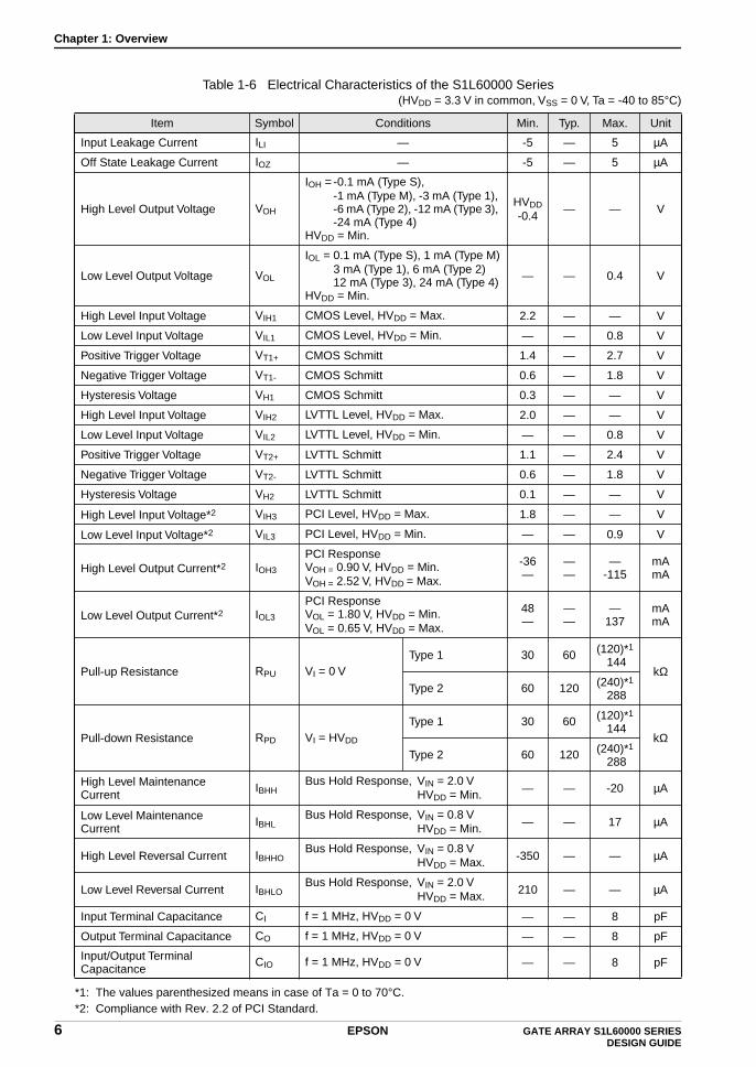
*1: The values parenthesized means in case of Ta = 0 to 70°C.*2: Compliance with Rev. 2.2 of PCI Standard.
Table 1-6 Electrical Characteristics of the S1L60000 Series(HVDD = 3.3 V in common, VSS = 0 V, Ta = -40 to 85°C)
Item Symbol Conditions Min. Typ. Max. Unit
Input Leakage Current ILI — -5 — 5 µA
Off State Leakage Current IOZ — -5 — 5 µA
High Level Output Voltage VOH
IOH = -0.1 mA (Type S), -1 mA (Type M), -3 mA (Type 1), -6 mA (Type 2), -12 mA (Type 3), -24 mA (Type 4)
HVDD = Min.
HVDD-0.4
— — V
Low Level Output Voltage VOL
IOL = 0.1 mA (Type S), 1 mA (Type M)3 mA (Type 1), 6 mA (Type 2)12 mA (Type 3), 24 mA (Type 4)
HVDD = Min.
— — 0.4 V
High Level Input Voltage VIH1 CMOS Level, HVDD = Max. 2.2 — — V
Low Level Input Voltage VIL1 CMOS Level, HVDD = Min. — — 0.8 V
Positive Trigger Voltage VT1+ CMOS Schmitt 1.4 — 2.7 V
Negative Trigger Voltage VT1- CMOS Schmitt 0.6 — 1.8 V
Hysteresis Voltage VH1 CMOS Schmitt 0.3 — — V
High Level Input Voltage VIH2 LVTTL Level, HVDD = Max. 2.0 — — V
Low Level Input Voltage VIL2 LVTTL Level, HVDD = Min. — — 0.8 V
Positive Trigger Voltage VT2+ LVTTL Schmitt 1.1 — 2.4 V
Negative Trigger Voltage VT2- LVTTL Schmitt 0.6 — 1.8 V
Hysteresis Voltage VH2 LVTTL Schmitt 0.1 — — V
High Level Input Voltage*2 VIH3 PCI Level, HVDD = Max. 1.8 — — V
Low Level Input Voltage*2 VIL3 PCI Level, HVDD = Min. — — 0.9 V
High Level Output Current*2 IOH3
PCI ResponseVOH = 0.90 V, HVDD = Min.VOH = 2.52 V, HVDD = Max.
-36—
——
—-115
mAmA
Low Level Output Current*2 IOL3
PCI ResponseVOL = 1.80 V, HVDD = Min.VOL = 0.65 V, HVDD = Max.
48—
——
—137
mAmA
Pull-up Resistance RPU VI = 0 VType 1 30 60 (120)*1
144kΩ
Type 2 60 120 (240)*1
288
Pull-down Resistance RPD VI = HVDD
Type 1 30 60 (120)*1
144kΩ
Type 2 60 120 (240)*1
288
High Level Maintenance Current
IBHHBus Hold Response, VIN = 2.0 V
HVDD = Min. — — -20 µA
Low Level Maintenance Current
IBHLBus Hold Response, VIN = 0.8 V
HVDD = Min. — — 17 µA
High Level Reversal Current IBHHOBus Hold Response, VIN = 0.8 V
HVDD = Max. -350 — — µA
Low Level Reversal Current IBHLOBus Hold Response, VIN = 2.0 V
HVDD = Max. 210 — — µA
Input Terminal Capacitance CI f = 1 MHz, HVDD = 0 V — — 8 pF
Output Terminal Capacitance CO f = 1 MHz, HVDD = 0 V — — 8 pF
Input/Output Terminal Capacitance
CIO f = 1 MHz, HVDD = 0 V — — 8 pF
6 EPSON GATE ARRAY S1L60000 SERIES DESIGN GUIDE
Chapter 1: Overview
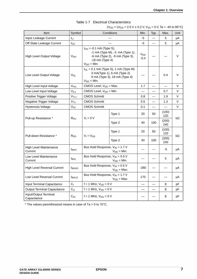
* The values parenthesized means in case of Ta = 0 to 70°C.
Table 1-7 Electrical Characteristics(VDD = LVDD = 2.5 V ± 0.2 V, VSS = 0 V, Ta = -40 to 85°C)
Item Symbol Conditions Min. Typ. Max. Unit
Input Leakage Current ILI — -5 — 5 µA
Off State Leakage Current IOZ — -5 — 5 µA
High Level Output Voltage VOH
IOH = -0.1 mA (Type S), -1 mA (Type M), -3 mA (Type 1), -6 mA (Type 2), -9 mA (Type 3), -18 mA (Type 4)
VDD = Min.
VDD
-0.4— — V
Low Level Output Voltage VOL
IOL = 0.1 mA (Type S), 1 mA (Type M)3 mA(Type 1), 6 mA (Type 2)9 mA (Type 3), 18 mA (Type 4)
VDD = Min.
— — 0.4 V
High Level Input Voltage VIH1 CMOS Level, VDD = Max. 1.7 — — V
Low Level Input Voltage VIL1 CMOS Level, VDD = Min. — — 0.7 V
Positive Trigger Voltage VT1+ CMOS Schmitt 0.8 — 1.9 V
Negative Trigger Voltage VT1- CMOS Schmitt 0.5 — 1.3 V
Hysteresis Voltage VH1 CMOS Schmitt 0.1 — — V
Pull-up Resistance * RPU VI = 0 VType 1 20 50
(100)120
kΩType 2 40 100
(200)240
Pull-down Resistance * RPD VI = VDD
Type 1 20 50(100)120
kΩType 2 40 100
(200)240
High Level Maintenance Current
IBHHBus Hold Response, VIN = 1.7 V
VDD = Min.— — -5 µA
Low Level Maintenance Current
IBHLBus Hold Response, VIN = 0.5 V
VDD = Min.— — 5 µA
High Level Reversal Current IBHHOBus Hold Response, VIN = 0.5 V
VDD = Max.-280 — — µA
Low Level Reversal Current IBHLOBus Hold Response, VIN = 1.7 V
VDD = Max.170 — — µA
Input Terminal Capacitance CI f = 1 MHz, VDD = 0 V — — 8 pF
Output Terminal Capacitance CO f = 1 MHz, VDD = 0 V — — 8 pF
Input/Output Terminal Capacitance
CIO f = 1 MHz, VDD = 0 V — — 8 pF
GATE ARRAY S1L60000 SERIES EPSON 7DESIGN GUIDE
Chapter 1: Overview
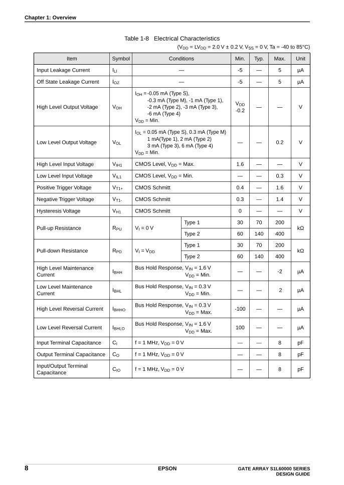
Table 1-8 Electrical Characteristics(VDD = LVDD = 2.0 V ± 0.2 V, VSS = 0 V, Ta = -40 to 85°C)
Item Symbol Conditions Min. Typ. Max. Unit
Input Leakage Current ILI — -5 — 5 µA
Off State Leakage Current IOZ — -5 — 5 µA
High Level Output Voltage VOH
IOH = -0.05 mA (Type S), -0.3 mA (Type M), -1 mA (Type 1), -2 mA (Type 2), -3 mA (Type 3), -6 mA (Type 4)
VDD = Min.
VDD
-0.2— — V
Low Level Output Voltage VOL
IOL = 0.05 mA (Type S), 0.3 mA (Type M)1 mA(Type 1), 2 mA (Type 2)3 mA (Type 3), 6 mA (Type 4)
VDD = Min.
— — 0.2 V
High Level Input Voltage VIH1 CMOS Level, VDD = Max. 1.6 — — V
Low Level Input Voltage VIL1 CMOS Level, VDD = Min. — — 0.3 V
Positive Trigger Voltage VT1+ CMOS Schmitt 0.4 — 1.6 V
Negative Trigger Voltage VT1- CMOS Schmitt 0.3 — 1.4 V
Hysteresis Voltage VH1 CMOS Schmitt 0 — — V
Pull-up Resistance RPU VI = 0 VType 1 30 70 200
kΩType 2 60 140 400
Pull-down Resistance RPD VI = VDD
Type 1 30 70 200kΩ
Type 2 60 140 400
High Level Maintenance Current
IBHHBus Hold Response, VIN = 1.6 V
VDD = Min.— — -2 µA
Low Level Maintenance Current
IBHLBus Hold Response, VIN = 0.3 V
VDD = Min.— — 2 µA
High Level Reversal Current IBHHOBus Hold Response, VIN = 0.3 V
VDD = Max.-100 — — µA
Low Level Reversal Current IBHLOBus Hold Response, VIN = 1.6 V
VDD = Max.100 — — µA
Input Terminal Capacitance CI f = 1 MHz, VDD = 0 V — — 8 pF
Output Terminal Capacitance CO f = 1 MHz, VDD = 0 V — — 8 pF
Input/Output Terminal Capacitance
CIO f = 1 MHz, VDD = 0 V — — 8 pF
8 EPSON GATE ARRAY S1L60000 SERIES DESIGN GUIDE

Chapter 1: Overview
HIDDS: The quiescent current between HVDD and VSS
LIDDS: The quiescent current between LVDD and VSS
Table 1-9 Quiescent Current (For Single Power Supplies)(Tj = 85°C)
Master2.5 V ± 0.2 V
IDDS Max.2.0 V ± 0.2 V
IDDS Max. Unit
S1L60093/60094S1L60173/60174S1L60283/60284
120 90 µA
S1L60403/60404S1L60593/60594S1L60833/60834
330 270 µA
S1L61233/61234S1L61583/61584
630 510 µA
S1L61903/61904S1L62513/62514
1000 800 µA
Table 1-10 Quiescent Current (For Dual Power supplies)(Tj = 85°C)
Master3.3 V ± 0.3 VHIDDS Max.
2.5 V ± 0.2 VLIDDS Max.
3.3 V ± 0.3 VHIDDS Max.
2.0 V ± 0.2 VLIDDS Max. Unit
S1L60093/60094S1L60173/60174S1L60283/60284
21 120 21 90 µA
S1L60403/60404S1L60593/60594S1L60833/60834
35 330 35 270 µA
S1L61233/61234S1L61583/61584
48 630 48 510 µA
S1L61903/61904S1L62513/62514
60 1000 60 800 µA
GATE ARRAY S1L60000 SERIES EPSON 9DESIGN GUIDE

Chapter 1: Overview
The value of quiescent current, except when chip temperature Tj = 85°C, can be estimated from the following formula: (Tj = - 40 to 85°C) (For Tj = 125°C, the estimated quiescent current is calculated from the temperature coefficient = 7. For Tj = 85 to 125°C, please consult Seiko Epson or its distributor.)
IDDS (Tj) = IDDS (Tj = 85°C) × Temperature coefficient
= IDDS (Tj = 85°C) × 10
(Example) The value of quiescent current of S1L61583 for VDD = 2.5 V ± 0.2 V and Tj = 50°C is estimated.
IDDS (Tj = 50°C) = IDDS (Tj = 85°C) × 10= 630 × 0.261= 164.43 (µA)
For the case of dual power supplies, the sum of the quiescent current for both of the voltages used is given as the total quiescent current (HIDDS + LIDDS).
Tj - 8560
50 - 8560
10 EPSON GATE ARRAY S1L60000 SERIES DESIGN GUIDE
Chapter 1: Overview
1.4 Overview of Gate Array Development Flow
Gate arrays are developed jointly by the customer and EPSON. System design, circuit design, and test pattern design is performed by the customer, based on various reference materials, including the cell libraries provided to the customer by EPSON.
When configuring an interface, customers are requested to present the required data and documents to Epson after confirming their validity against the data release checklist provided in Appendix A1.
Customers are expected to performs simulation, analysis and other necessary work on the target project using available software and EPITS (*1). When the customer has completed this work, Seiko Epson will undertake placement and writing work on that project.
Note: *1 : EPITS is Seiko Epson’s ASIC design support system that runs on MS-Windows NT4.0 or SUN-Solaris platforms. It does not include any simulation or synrhesis functions.
The simulation is currently supported by the following EDA software:
• Verilog-XL (*1)
• ModelSim (*2)
Note: *1 :Verilog-XL is a registered trademark of Cadence Desgin Systems Corporation, USA.
*2 :ModelSim is a registered trademark of Model Technology Corp., USA.
For more information, contact to our sales office for technical support.
GATE ARRAY S1L60000 SERIES EPSON 11DESIGN GUIDE
Chapter 1: Overview
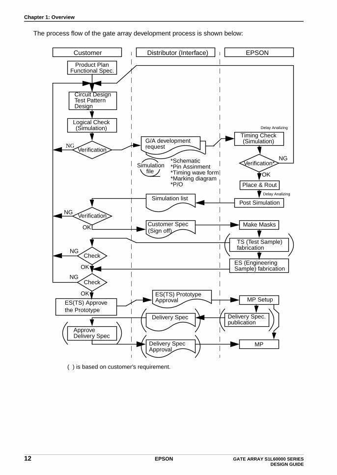
The process flow of the gate array development process is shown below:
Customer Distributor (Interface) EPSON
Product Plan
Circuit Design
Logical Check
Verification
Timing Check
Verification*
Place & Rout
Post Simulation
G/A developmentrequest
*Schematic*Pin Assinment*Timing wave form*Marking diagram*P/O
Simulation list
Customer Spec(Sign off)
Verification
Make Masks
TS (Test Sample)fabrication
ES (EngineeringSample) fabrication
MP Setup
Delivery Spec.publication
MP
Delivery Spec
Delivery SpecApproval
ApproveDelivery Spec
(Simulation)
(Simulation)
Test PatternDesign
Functional Spec.
NG
NG
OK
OK
NG
OK
NG
NG
Check
Check
( ) is based on customer’s requirement.
ES(TS) PrototypeApprovalES(TS) Approve
the Prototype
OK
Delay Analizing
Simulationfile
Delay Analizing
12 EPSON GATE ARRAY S1L60000 SERIES DESIGN GUIDE

Chapter 2: Estimating Gate Density and Selecting the Master
Chapter 2 Estimating Gate Density and Selecting the Master
Methods and guidelines are described below to assist in defining the logic which will be integrated into a gate array, estimating the array requirements, and determining the appropriate master for a given application.
2.1 Dividing Up Logic Between Chips
When extracting logic, which is to be integrated into gate arrays from the system being created by the user, the logic should be selected with the following criteria in mind.
• Integration Criteria
(1) Logic size to be integrated (Gate count)(2) Number of I/O pins required (Pin count)(3) Package to be used(4) Power consumption
Generally, the larger the gate size, the more power is consumed, and the more input and output terminals required. Because of this, it may be better, from the perspective of total cost or from the perspective of power consumption, etc., to divide the circuit into multiple chips, rather than forcing them into a single chip.
2.2 Determining Gate Size
In the case of gate arrays, the scope of the array is defined as the sum of gates or basic cells (BCs) used. The number of BCs for each cell is listed in the Gate Array S1L60000 Series MSI Cell Library. Be sure to consult this library to determine the total number of BCs in your circuit.
2.3 Estimating the Number of Input/Output Pins
After estimating the number of BCs used, calculate the number of input/output pins actually used. Be sure to include RAM test pins and power supply pins in the pin count. Estimate the number of power supply pins using the method discussed in Chapter 10.
GATE ARRAY S1L60000 SERIES EPSON 13DESIGN GUIDE
Chapter 2: Estimating Gate Density and Selecting the Master
2.4 Selecting the Master
Select the appropriate master from Table1-1, based on the estimated number of BCs, the number of required input and output pins (including power supply pins) and the package to be used.
The actual number of BCs (BCA) which can be used for each device type is estimated using the following formula from the gross number of BCs (BCG) loaded on each master (shown in Table 1-1 of the previous chapter) and the cell utilization ratio (U).
BCA = U × BCG
NOTE: When a RAM circuit is included, this estimate should be made after refering to the following section and after refering to Chapter 5.Also when a circuit is used by dual power, the estimate should be made after refering to Chapter 11.
2.5 Estimating the BCs That Can Be Used in Circuits Which Include RAM
RAM blocks, in comparison to MSI cells, are extremely large and have fixed shapes (defined vertical and horizontal dimensions). Because of this, some RAM blocks which may appear to fit on the chip because of calculations based on the number of BCs may, in actuality, not be placable on a given master. Thus, the first decision is that of whether or not the RAM configuration is available on a given master. Please refer to Chapter 5.
Once the masters which can accommodate the RAM have been selected, it becomes possible to estimate the number of BCs (BCAWR) of random logic (excluding RAM) available using the formula below.
BCAWR = 0.9 × U × (BCG - BCRAM)
where BCAWR is the number of BCs available for random logicBCG is the total BCs available on a mater (raw gates)BCRAM is the BC use of RAM(s) (See Chapter 5 for BC calculation)U is the utilization ratio.
NOTE: Actual BCs available (BCAWR) is design dependent.Use the formula above for estimation purposes only.Please consult EPSON for design specific information.
14 EPSON GATE ARRAY S1L60000 SERIES DESIGN GUIDE

Chapter 3: Cautions and Notes Regarding Circuit Design
Chapter 3 Cautions and Notes Regarding Circuit Design
3.1 Inserting I/O Buffers
All external (or primary) input, output and bi-directional signals must be attached to I/O buffers. Due to CMOS IC’s extreme vulnerability to electrical static discharge (ESD), protection circuitry has been incorporated within the I/O buffers to ensure device reliability and quality.
3.2 The Use of Differentiating Circuits is Forbidden
The propagation delay (tpd) of internal cells within a gate array vary, depending on process variance during mass production and environment variance during device usage. Differentiating circuits such as the one shown in Figure 3-1 should be avoided due to difficulties associated with control of the resultant pulse width relative to variances in propagation delays through each logic element.
Figure 3-1 Example of a Differentiating Circuit
3.3 Wired Logic is Forbidden
Wired logic, available in bipolar devices, is not allowable in the S1L60000 Series, a CMOS technology. Consequently, cell output pins cannot be wired together, such as shown in Figure 3-2, with the exception of internal 3-state bus elements.
Figure 3-2 Examples of Forbidden Wired Logic
GATE ARRAY S1L60000 SERIES EPSON 15DESIGN GUIDE

Chapter 3: Cautions and Notes Regarding Circuit Design
3.4 Hazard Countermeasures
In circuits such as decoders and multiplexors which are structured from combinational functions such as NAND gates or NOR gates, extremely short pulses can be produced by differences in the gate delay times. These short pulses are called hazards, and when these hazards propagate to clock, reset or reset pins of FFS (Flip Flop), malfunctions may occur.
Because of this, it is necessary to use caution when designing circuits which may produce hazards, creating circuit structures which do not propagate hazards, having decoder circuits with “enable” terminals, etc.
3.5 Limitations on Logic Gate Output Load
With CMOS circuits, signal propagation time (tpd) and signal rise and fall times (tslew) characteristically increase as load capacitance of the output increases.
Cell propagation delay is determined, in part, by the load capacitance at the output terminals. When the load capacitance is too large, the propagation delay increases, and malfunctions may result. Because of this, there are limitations on the number of loads which can be connected to the output terminals of each cell, and these limitations are referred to as “fan-out constraints”.
The input terminal capacitance of each gate differs from gate input to gate input. The input capacitance of each gate input is defined relative to the input capacitance of an inverter (IN1 which is defined as being equal to 1) is called the “fan-in”.
Circuits should be designed so that the sum of the fan-ins connected to the output terminals of each gate does not exceed the fan-out constraints of that output terminal.
Also, high speed clock lines (f max = 60 MHz or more), should be designed so that the output terminal load of the associated logic gates is about half of the fan-out constraints to ensure high performance.
In the actual LSI circuit layout, both the input capacitance of the next-stage gate and the wiring capacitance of a signal are applied as load capacitance. Because accurate wiring capacitance is determined by the placement and routing of a circuit, the placement and routing may result in the application of a large load capacitance to a specific node. The conditions of the loads on each circuit node can be determined by the output results of tslew. Please note that if the output of tslew exceeds the standard value, we may request circuit modification in order to keep it within the specified limit. To control increases in the load capacitance following the placement and routing of the circuit, the number of circuit branches within a single node should be kept as low as possible and, if branches exist, buffers with a higher number of fan-outs should be used.
3.6 Bus Circuits
Internal 3-state bus circuits are constructed, using 3-state logic gates. The 3-state logic gates output terminals can be wired together if at all times one, and only one 3-state logic gate is active at a given time (while the remaining 3-state logic gate outputs are put in high impedance state). This circuit allows multiple signal sources to share a given net at different time intervals during circuit operation.
16 EPSON GATE ARRAY S1L60000 SERIES DESIGN GUIDE

Chapter 3: Cautions and Notes Regarding Circuit Design
Please keep the following recommendations in mind when bus circuits are used:
Notes Regarding the Use of Bus Circuits:
(1) Bus cells cannot be used except in bus circuits. (Please refer to Table 3-1 regarding S1L60000 Series bus cells.)
(2) When bus cells are used, please attach one (and only one) BLT cell (bus latch) to each 3-state bus net.
(3) A maximum of 32 bus cells can be attached to a single bus. (Fan-out = 32)
(4) One, and only one, 3-state cell can be active (output terminal driving a logic 0 state or logic 1 state) at a time. All other 3-state bus cells connected to that net must be inactive (output terminal in high impedance Z state).
(5) If all 3-state bus cells are inactive (output terminals in high impedance Z state) on a given bus net, the BLT (bus latch) will maintain the last valid state (either logic 1 state or logic 0 state). The BLT function is merely to avoid bus floating, therefore, the processing of internal 3-state bus latch data must be performed while 3-state bus drivers are active rather than processing data while BLTs control bus data.
(6) In order to improve testability, design the 3-state bus such that it can be initialized easily and quickly during device testing. This can be done by utilizing a separate test pin to control the 3-state bus, or by instantiating default 3-sate bus drivers.
(7) The 3-state cell control terminals must change only once during a single test vector event (cycle) to allow test vector set usage during IC device testing.
(8) High speed 3-state bus operation may be inhibited by large fan-out loading on 3-state bus drivers.
Table 3-1 shows a table of the bus cells which can be used in the S1L60000 Series.
Table 3-1 S1L60000 Series Bus Cells
Cell TypeCell Name
1 Bit 4 Bit 8 Bit
Bus latches BLT 1 BLT 4 BLT 8
Bus driverTSB, TSB4,TSB8, TSBP
T244H T244
Inverting bus driverTSV, TSV4,TSV8, TSVP
T240H T240
Transparent latches with reset and 3-state output
— T373H T373
D-flip flops with rest and3-state output
— T374H T374
1-bit RAM RM1 — —
GATE ARRAY S1L60000 SERIES EPSON 17DESIGN GUIDE

Chapter 3: Cautions and Notes Regarding Circuit Design
Figure 3-3 Example of Bus Cell Circuit Structure
3.7 Bus Hold Circuits
In the S1L60000 Series, I/O buffers with an added bus hold function (to maintain the output signal pin data) have been provided, so that output signal pin (or bi-directional signal pin) does not enter high-impedance state.
However, to prevent these circuits from affecting normal operation, the latching capability of the bus hold circuit is weak; thus, the stored data output should not be used as valid data. This pin state can be overriden easily by an externally supplied signal.
Please refer to Tables 1-6 to 1-8 regarding the output maintenance current of the bus hold circuit.
Figure 3-4 Examples of Structures of Bus Hold Circuits
3.8 Schematic Capture Guidelines
Please adhere to the following conventions when designing an ASIC via manual schematic entry:
• Use logic cells found in Gate Array S1L60000 Series MSI Cell Library.
• Use orthogonal (not oblique) connections when wiring logic cells to one another.
• Primary uni-directional I/O and bi-directional I/O signal names must be 2 to 32 characters in length, and must begin with an alphabetic character.
BLT1
TSB
TSB
NA2
IN1
TB1HT
A
E
TA
for Test
Output signal
OutputTE
TS
Enable
(a) Output buffer (b) Bi-directional buffer
BC1HT
A
E
TA Bi-directionalTE
TS
Input signal
Enable
Output signal
for Test
18 EPSON GATE ARRAY S1L60000 SERIES DESIGN GUIDE

Chapter 3: Cautions and Notes Regarding Circuit Design
3.9 Clock Tree Synthesis
(1) Overview
Clock Tree Synthesis is a support that automatically inserts the ClockTree into the buffer group that optimizes the skew and delay time of “ClockLine”. If a customer has a program to insert ClockTree to adjust the Fan-out of “ClockLine”, clock skew may be large, so the P & R tool is started and the placing and routing for designing the gate array are executed voluntarily. Also, the propagation delay time may be longer than estimated because there are many cases it is difficult to maintain a good balance between the wire interconnecting load and the intrinsic cell delay. The Clock Tree Synthesis is used to solve this problem.
Also, for circuits that contain Gating Cells (simple gates) in Clock Lines, we can optimize Clock Line skew and delay values. (The synthesis method applied to Clock Lines that include Gating Cells is known as Gated Clock Tree Synthesis.)
To insert Clock Tree Synthesis, the customer must insert the special buffer to the Clock Line for the following three purposes.
• Judging the place to insert the Clock Tree Synthesis.
• Estimating the delay time of the Clock Tree inserted and execute the simulation of virtual wire interconnecting level (pre-simulation).
• Back annotate the delay time of the inserted Clock Tree to accurately estimate the post-simulation.
(2) How to Examine the Clock Tree Synthesis
Select the special buffer for the Clock Tree Synthesis in Table 3-3 and the special Gating Cell for Gated Clock Tree Synthesis in Table 3-4. Then insert the special buffer selected from the table into the Clock Line taking into consideration the restriction or notes mentioned later and the same placing as the normal cells (Refer to Figures 3-5 and 3-6). Otherwise, if the logic are designed by HDL, as the special buffer can not insert automatically the Clock Line, assign directly the HDL of the content using the script language. Note that another buffer is not combined in the clock Line inserted in the special buffer, and execute the following command:
set_don’t_touch_net net_name
Note: For cases with Gating Cells, the skew value varies significantly depending on the number of Gating Cells and other factors. If the number of Gating Cells is high, contact EPSON for skew values.
Table 3-2 Guidance for Skew Values
Guidance for the number of fan-outs Without Gating Cells [ps] With Gating Cells [ps]
0–500 ±200 ±300
500–3000 ±250 ±400
3000–10000 ±300 ±500
10000– ±350 ±600
GATE ARRAY S1L60000 SERIES EPSON 19DESIGN GUIDE

Chapter 3: Cautions and Notes Regarding Circuit Design
[The special buffer]
Select the special buffer from the table below corresponding to the estimated number of fan-outs.
Note 1: The value “K” (load delay of fan-out) of these cells is set “0” at the pre-simulation.
Note 2: The number of fan-outs of these cells is set to the infinity.
Note 3: Please consider that the load delay for the number of fan-outs is not accurately and only estimated.
Note 1: The load delay value (To) of these cells is set “0” at the pre-simulation.
Note 2: The value “K” (load delay of fan-out) of these cells is set “0” at the pre-simulation.
Note 3: The number of fan-outs for these cells is set to infinity.
Table 3-3 The Special Buffers for S1L60000
Cell Name To Max (ns) Estimated number of fan-out
CRBF2 2.00 0 to 500
CRBF3 3.00 500 to 3000
CRBF4 4.00 3000 to 10000
CRBF5 5.00 Over 10000
CRBF6 6.00
CRBF7 7.00
CRBF8 8.0
Table 3-4 The Special Gating Cell Names
Function Cell Name
AND CAD2V
OR COR2V
2-1 Selector CAO24AV
NAND CNA2V
NOR CNO2V
2-1 Selector CAN24A
INVERTER CGIN4
20 EPSON GATE ARRAY S1L60000 SERIES DESIGN GUIDE
Chapter 3: Cautions and Notes Regarding Circuit Design
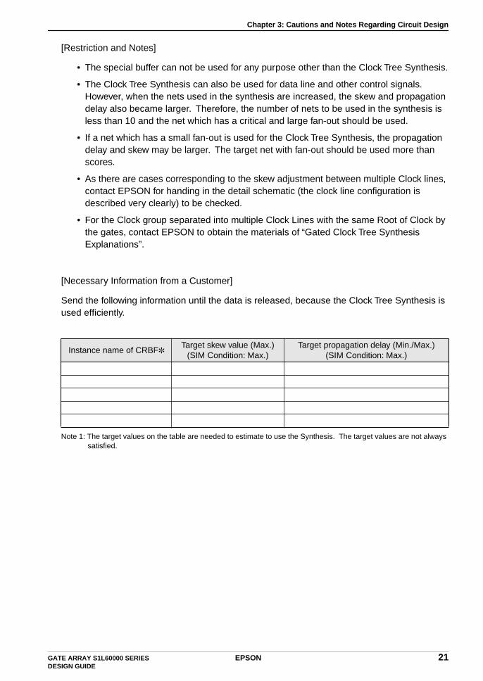
[Restriction and Notes]
• The special buffer can not be used for any purpose other than the Clock Tree Synthesis.
• The Clock Tree Synthesis can also be used for data line and other control signals. However, when the nets used in the synthesis are increased, the skew and propagation delay also became larger. Therefore, the number of nets to be used in the synthesis is less than 10 and the net which has a critical and large fan-out should be used.
• If a net which has a small fan-out is used for the Clock Tree Synthesis, the propagation delay and skew may be larger. The target net with fan-out should be used more than scores.
• As there are cases corresponding to the skew adjustment between multiple Clock lines, contact EPSON for handing in the detail schematic (the clock line configuration is described very clearly) to be checked.
• For the Clock group separated into multiple Clock Lines with the same Root of Clock by the gates, contact EPSON to obtain the materials of “Gated Clock Tree Synthesis Explanations”.
[Necessary Information from a Customer]
Send the following information until the data is released, because the Clock Tree Synthesis is used efficiently.
Note 1: The target values on the table are needed to estimate to use the Synthesis. The target values are not always satisfied.
Instance name of CRBFTarget skew value (Max.)
(SIM Condition: Max.)Target propagation delay (Min./Max.)
(SIM Condition: Max.)
GATE ARRAY S1L60000 SERIES EPSON 21DESIGN GUIDE

Chapter 3: Cautions and Notes Regarding Circuit Design
Yes No1. Is the number of Clock Lines 10 or fewer? .......................................................... •
Yes No2. Does the Clock Net include a dedicated Gating Cell?......................................... •
If you answered Yes to the question 2, above, answer questions 3 through 8 below.
Yes No3. Is the number of dedicated Gating Cells included in each Clock Net 10 or fewer?
............................................................................................................................. •
Yes No4. Is the number of dedicated gated cell stages 2 or fewer? ................................... •
Yes No5. Does the Clock Net include any cell other than Gating Cells? ............................ •
Note: If the Clock Net contains any cell other than Gating Cells, Clock Tree Synthesis requires a special procedure. Please consult Epson if you have any cell other than Gating Cells in your Clock Nets.
Yes No6. Is Clock Tree Synthesis applied to cells other than DFFs and latches? .............. •
If Yes, write the cell names below.
Yes No7. Is there a circuit configuration similar to the one in Figure 3-7? .......................... •
Yes No8. Is there a circuit configuration similar to the one in Figure 3-8? .......................... •
Note: Make corrections by referring to the processing examples for problem circuits below (Figures 3-7 and 3-8).
22 EPSON GATE ARRAY S1L60000 SERIES DESIGN GUIDE
Chapter 3: Cautions and Notes Regarding Circuit Design
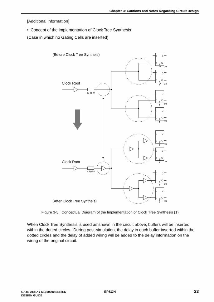
[Additional information]
• Concept of the implementation of Clock Tree Synthesis
(Case in which no Gating Cells are inserted)
Figure 3-5 Conceptual Diagram of the Implementation of Clock Tree Synthesis (1)
When Clock Tree Synthesis is used as shown in the circuit above, buffers will be inserted within the dotted circles. During post-simulation, the delay in each buffer inserted within the dotted circles and the delay of added wiring will be added to the delay information on the wiring of the original circuit.
D
C
DFFF
Q
XQ
D
C
DFFF
Q
XQ
D
C
DFFF
Q
XQ
D
C
DFFF
Q
XQ
D
C
DFFF
Q
XQ
D
C
DFFF
Q
XQ
D
C
DFFF
Q
XQ
D
C
DFFF
Q
XQ
CRBF
Clock Root
(Before Clock Tree Syntheis)
(After Clock Tree Syntheis)
CRBF
Clock Root
GATE ARRAY S1L60000 SERIES EPSON 23DESIGN GUIDE

Chapter 3: Cautions and Notes Regarding Circuit Design
• Concept of the implementation of Clock Tree Synthesis
(Case in which no Gating Cells are inserted)
Figure 3-6 Conceptual Diagram of the Implementation of Clock Tree Synthesis (2)
When Clock Tree Synthesis is used as shown in the circuit above, buffers will be inserted within the dotted circles. During post-simulation, the delay in each buffer inserted within the dotted circles and the delay of added wiring will be added to the delay information on the wiring of the original circuit.
D
C
DFFF
Q
XQ
D
C
DFFF
Q
XQ
D
C
DFFF
Q
XQ
D
C
DFFF
Q
XQ
D
C
DFFF
Q
XQ
D
C
DFFF
Q
XQ
D
C
DFFF
Q
XQ
D
C
DFFF
Q
XQ
CRBF
Clock Root
(Before Clock Tree Syntheis)
(After Clock Tree Syntheis)
CRBF
Clock Root
V
CAD2V
V
CAD2V
24 EPSON GATE ARRAY S1L60000 SERIES DESIGN GUIDE
Chapter 3: Cautions and Notes Regarding Circuit Design
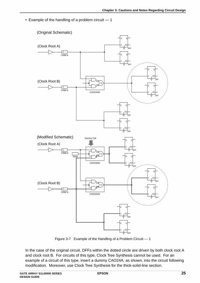
• Example of the handling of a problem circuit — 1
Figure 3-7 Example of the Handling of a Problem Circuit — 1
In the case of the original circuit, DFFs within the dotted circle are driven by both clock root A and clock root B. For circuits of this type, Clock Tree Synthesis cannot be used. For an example of a circuit of this type, insert a dummy CAO24A, as shown, into the circuit following modification. Moreover, use Clock Tree Synthesis for the thick-solid-line section.
D
C
DFFF
Q
XQ
D
C
DFFF
Q
XQ
D
C
DFFF
Q
XQ
D
C
DFFF
Q
XQ
D
C
DFFF
Q
XQ
D
C
DFFF
Q
XQ
CRBF
(Clock Root A)
CRBF
(Clock Root B)
(Original Schematic)
(Modified Schematic)
V
CAO24AV
D
C
DFFF
Q
XQ
D
C
DFFF
Q
XQ
D
C
DFFF
Q
XQ
D
C
DFFF
Q
XQ
D
C
DFFF
Q
XQ
D
C
DFFF
Q
XQ
CRBF
PDW
Dummy Cell
(Clock Root A)
CRBF
(Clock Root B)V
CAO24AV
V
CAO24AV
GATE ARRAY S1L60000 SERIES EPSON 25DESIGN GUIDE

Chapter 3: Cautions and Notes Regarding Circuit Design
• Example of the handling of a problem circuit — 2
Figure 3-8 Example of the Handling of a Problem Circuit — 2
The DFFs in dotted circles in the above diagram are driven by both clock root A and clock root B. For circuits of this type, Clock Tree Synthesis cannot be used. In such a case, remove the CRBF cell from the clock root B.
D
C
DFFF
Q
XQ
D
C
DFFF
Q
XQ
D
C
DFFF
Q
XQ
D
C
DFFF
Q
XQ
CRBF
(Clock Root A)
CRBF
(Clock Root B)V
CAO24AV
Please Delete
26 EPSON GATE ARRAY S1L60000 SERIES DESIGN GUIDE
Chapter 3: Cautions and Notes Regarding Circuit Design
3.10 ATPG (Auto Test Pattern Generation)
(1) Introduction
The so-called “ATPG” means tools to automatically generate test patterns that are released by tool-producing vendors. The “TestGen” of the tool executed to “ATPG” supplied by Synopsys Inc. and Sunrise Inc. is used in ASIC design at EPSON. By using “TestGen”, the scanning circuit can be inserted to the original circuit and the test patterns can be generated automatically.
The word “control” described in this chapter is used to specify free level to the target pin without passing to the sequential circuit. This “control” meaning should be noted because it can not be used for dividing clocks and so on needed in some cycles to set the state. For example, when using “control” where a clock of each flip-flop circuit can be controlled externally, the circuit means that the external input clock (an original signal) can reach each flip-flop circuit.
(2) Outline
When the scanning circuit is inserted into the design ruled circuit for “ATPG” support, some faults are detected in the circuit when using the “ATPG” tool. However, internal nodes are forced to move from external pins through the scanning circuit and are observed. Therefore, the test patterns outputted from the “ATPG” tool can not be used to check the operations of the user’s circuit.
Users need to create the test patterns to check the standard operations of their circuit. The test patterns outputted from the “ATPG” tool can only be used to reach the level of the fault detecting rate in the circuit.
When using the “ATPG” tool, the test patterns to get 100% of fault detecting can be generated, except that nodes can not to be tested and faults can not be tested logically. The “ATPG” method is adapted to full scanning using “MUXSCAN type FF (Flip-flop)”.
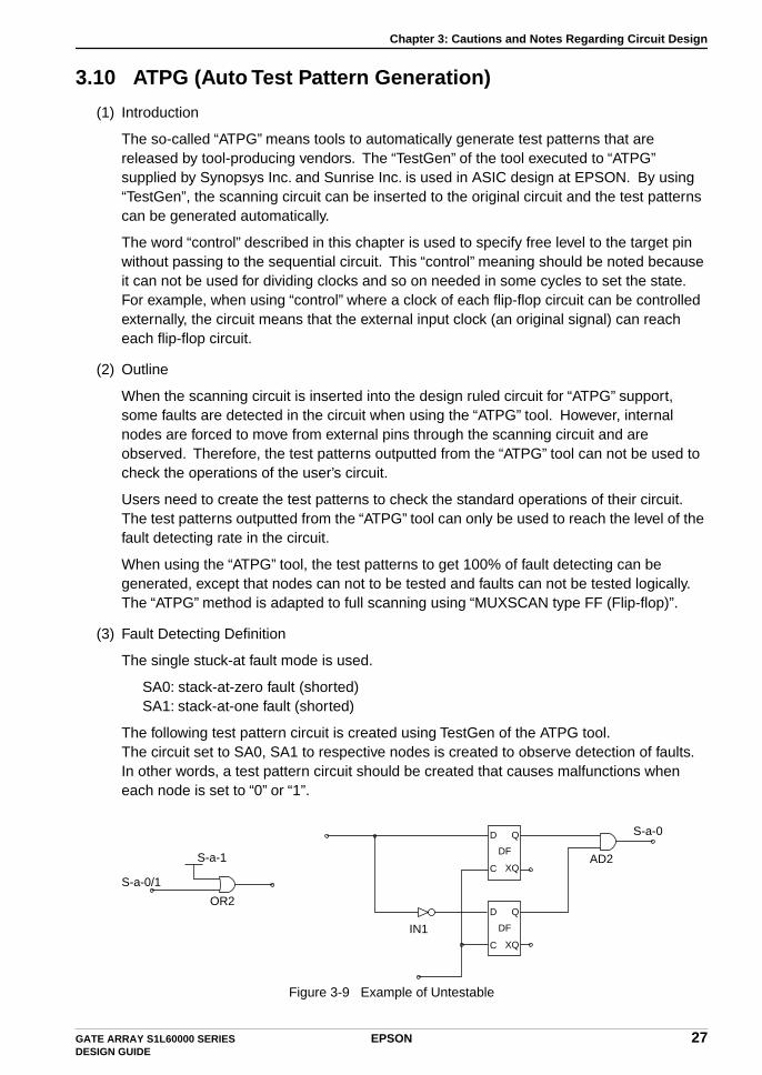
(3) Fault Detecting Definition
The single stuck-at fault mode is used.
SA0: stack-at-zero fault (shorted)SA1: stack-at-one fault (shorted)
The following test pattern circuit is created using TestGen of the ATPG tool.The circuit set to SA0, SA1 to respective nodes is created to observe detection of faults. In other words, a test pattern circuit should be created that causes malfunctions when each node is set to “0” or “1”.
Figure 3-9 Example of Untestable
S-a-1
S-a-0/1
OR2
IN1
D
C
DF
S-a-0
AD2
Q
XQ
D
C
DF
Q
XQ
GATE ARRAY S1L60000 SERIES EPSON 27DESIGN GUIDE

Chapter 3: Cautions and Notes Regarding Circuit Design
(4) Design Flow
Figure 3-10 ATPG flow when designing by logic synthesis
ATPG Rule Check
Seiko EpsonCustomer
APTGApplication Note
Dummy NetlistAPTG
Check Sheet
Verification
Logical check
Netlist Circuit Data
ATPG
HDL Design
Verilog-XL
RTL Creation TP Creation
ATPG Rule Check
Logic Synthesis
Pre-Simulation
ATPG Rule Check
ATPG Rule Check
Insert Scanning
Fault Detection
OK or N.G
P & R
P & R
Clock Tree Synthesys
Post-Simulation
Post-Simulation
Result List
Post-SimulationVerification
Sign off
TemporarySchematic
Pin AssignmentCircuit Block
Diagrams
Expected Valuesof Input Patters Netlist Circuit Data Schematic
Pin Assignment
Verification after ATPG
Verification ofFault Detection Rate
28 EPSON GATE ARRAY S1L60000 SERIES DESIGN GUIDE
Chapter 3: Cautions and Notes Regarding Circuit Design
(5) Test pattern composition created by ATPG
There are two test patters generated by ATPG, and their modes must be exchanged at the scanning enable input pin (SCANEN). The SCANEN pin needs to be used as the dedicated input pin because it is connected when the circuit is scanned.
• Scanning shift modeThis mode is used when the memory element (scan FF) in the circuit composed for the shift register is inputted or outputted data.
• Scanning test modeThis mode is used when the data inputted to the memory element on the scanning shift mode is used to operate on the circuit by the clock input.
(6) I/O Pins for ATPG
If two pins of SCANEN and ATPGEN are used, the ATPG can execute very efficiently. As a result, the delivery time is shortened and the fault detection rate goes up. The following explanation describes the pins needed to execute the ATPG.
• Scan Enable Input Terminal (SCANEN)This pin is used to exchange the scan shift mode with the scan test mode. It is also used when resetting or setting to FF (Flip Flop) and to fix the bi-directional I/O exchange signals while shifting each FF to scan. This pin must be ready for the dedicated pin because it is definitely needed to scan FF.
• Test input pin for ATPG (ATPGEN)This pin is used to make the circuit suitable for ATPG. For example, the asynchronous part of the circuit should be fixed by using the test input pin and if the clock line cannot be controlled externally, it can be controlled by using the pin for exchange. If the original circuit is adequate to the rule of ATPG, the pin is not needed for ATPG and the dedicated pin is used.
• Scan data input pinThis scan data input pin is used to set the data to the shift register generated by scanning FF. In case of multi-scan FF, the number of scan data input pins is increased. These pins can be shared with others. However, they can not be used to share with the control pin to set or reset to the scan data or the clock and other pins to scan FF. If the scan data input pins are used to share with the bi-directional pins, they should be designed to be always used for input by utilizing the ATPGEN pin.
• Scan data output pinThis scan data output pin is used to read the data from the shift register generated by scanning FF. In case of multi-scan FF, the number of scan data output pins is increased. These pins can be shared with other pins. If the scan data output pins are used to share with bi-directional pins, they should be designed to be always used for output by considering utilizing the ATPGEN pin.
• Scan clock input pinThis pin is the clock input pin at the test pattern generated by ATPG. This pin usually utilizes the system clock in normal operation.
GATE ARRAY S1L60000 SERIES EPSON 29DESIGN GUIDE
Chapter 3: Cautions and Notes Regarding Circuit Design
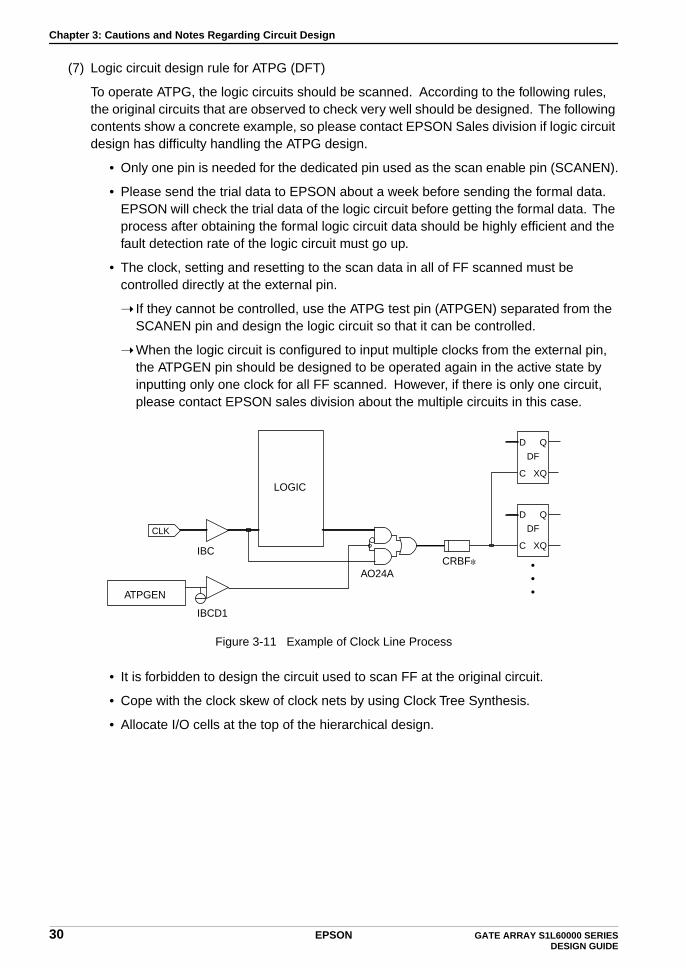
(7) Logic circuit design rule for ATPG (DFT)
To operate ATPG, the logic circuits should be scanned. According to the following rules, the original circuits that are observed to check very well should be designed. The following contents show a concrete example, so please contact EPSON Sales division if logic circuit design has difficulty handling the ATPG design.
• Only one pin is needed for the dedicated pin used as the scan enable pin (SCANEN).
• Please send the trial data to EPSON about a week before sending the formal data. EPSON will check the trial data of the logic circuit before getting the formal data. The process after obtaining the formal logic circuit data should be highly efficient and the fault detection rate of the logic circuit must go up.
• The clock, setting and resetting to the scan data in all of FF scanned must be controlled directly at the external pin.
If they cannot be controlled, use the ATPG test pin (ATPGEN) separated from the SCANEN pin and design the logic circuit so that it can be controlled.
When the logic circuit is configured to input multiple clocks from the external pin, the ATPGEN pin should be designed to be operated again in the active state by inputting only one clock for all FF scanned. However, if there is only one circuit, please contact EPSON sales division about the multiple circuits in this case.
Figure 3-11 Example of Clock Line Process
• It is forbidden to design the circuit used to scan FF at the original circuit.
• Cope with the clock skew of clock nets by using Clock Tree Synthesis.
• Allocate I/O cells at the top of the hierarchical design.
CLK
IBC
IBCD1
ATPGEN
LOGIC
AO24ACRBF
D Q
C XQ
DF
D Q
C XQ
DF
30 EPSON GATE ARRAY S1L60000 SERIES DESIGN GUIDE

Chapter 3: Cautions and Notes Regarding Circuit Design
• Do not use the internal 3-state bus.
The internal 3-state bus should be composed of the multiplexer and so on. However, if the circuit design needs an internal 3-state bus by any means, use the ATPGEN pin and the bus circuit must be designed never to cause a contention. When the circuit is designed by using the internal 3-state bus, the fault detection rate in the circuit does not always go up. Please contact EPSON sales division if a high fault detection rate is desired (Refer to Figure 3-13).
Figure 3-12 Process Example of Internal 3-state
• When using the macro cells, for example — RAM, ROM, Mega cell and so on, design the circuit inserted in the scanned FF before or after the I/O ports of the macro cells.
If circuit design is impossible, the faults can not often be detected before or after the macro cells.
• Keep away using MSI macro cells included in the Flip Flop, for example — T175, A161 and so on.
The MSI cells can not scan. Do not use them if a high fault detection rate is desired.
• Do not use the asynchronous circuit and a circuit that causes racing at the RS latch, differentiating circuit and so on.
If these circuits are used, fix their output by using the ATPGEN pin. Furthermore, as the fault detection rate is not always up, do not use the circuit if a high fault detection rate is desired.
• Fix the latch cell by using the ATPGEN so that it is always through.
As the fault detection rate is not always up, do not use the circuit if a high fault detection rate is desired.
• Design the bi-directional pin to be state of input in the scan shifting mode.
If the bi-directional pin must be assigned to the scan data input and output pins, fix it to be state of each condition (Refer to Figure 3-14).
IBCD1
ATPGEN
Z1BLT1
TSB
TSB
GATE ARRAY S1L60000 SERIES EPSON 31DESIGN GUIDE

Chapter 3: Cautions and Notes Regarding Circuit Design
Figure 3-13 Process Example of bi-directional pins
• Fix the FF so that it is not scanned
As the T-FF, MSI macro cells include the FF, and the output from the FF not to be scanned causes a malfunction in the ATPG test patterns. Also, fault detection of the circuit often can not be executed, so if possible they should be fixed by the ATPGEN.
(8) Others
• The number of gates goes up about 15 to 20% compared to the original circuit, but it depends on the number of scanned FFs.
• The fault detection rate at the scanned FF depends on the circuit configuration and the scale of gates. At least three working days are needed for DFT and ATPG at EPSON. (In an unusual case, about ten working days may be needed depending on the circuit configuration. Please refer to this book for the circuit configuration before designing it.)
• Please send the papers on “ATPG check sheet” and “External pin information” to EPSON before sending the logic circuit data. If there are problems with the logic circuit, EPSON may ask to change the design. Please define the external pins (ATPGEN, SCANEN and so on) added to scan FFs at the test patterns interfaced to EPSON. Please send the “CTS Application/On Notes” attached sheet at the same time, because when placing cells and routing interconnections, they are requested to cope with CTS (Clock Tree Synthesis).
IBCD1
ATPGEN
IBCD1
BC1
BC1
BC1
AE
AE
AE
D1
D0
D2
SCANOUT
SCANIN
SCANEN
32 EPSON GATE ARRAY S1L60000 SERIES DESIGN GUIDE

Chapter 3: Cautions and Notes Regarding Circuit Design
(9) ATPG check sheet
Never delay sending this sheet a week before sending the logic circuit data. Please mark “Yes” or “No” at each item.
1. Which the netlist format (gate level) interfaced to EPSON? Verilog or EDIF
2. Is the scanned FF used at the original circuit? (Note 1) Yes or No
3. Do you use macro cells, MSI cells and interval oscillator cells? Yes or No
4. If you answer “Yes” to the question above, write the cell name. :
5. Do you use the internal 3-state bus? Yes or No
6. Does your logic circuit have RS latch,differential circuit and asynchronous circuit? Yes or No
7. Do you use latch cells? Yes or No
8. Is there a bi-directional pin? Yes or No
9. Are there clocks that can not be directly controlled externally? Yes or No
10. Are there FF, reset and set pins of latch cellsthat can not be directly controlled externally? Yes or No
11. If the answers are “Yes” to question Nos.3 to 10, does thecircuit design correspond to the DFT rule? (Note 2) Yes or No
12. Are I/O cells arranged on the top of the hierarchy? Yes or No
13. Do the clocknets cope with skew by CTS? Yes or No
Note1: If you answered “Yes”, please design the logic circuit again, because the circuit can not scan.
Note2: If you answered “No”, please insert the DFT, because the circuit can not scan. Also, if you ask to insert the DFT to EPSON, please contact EPSON sales division, because circuit information in addition to that on this sheet is required.
GATE ARRAY S1L60000 SERIES EPSON 33DESIGN GUIDE

Chapter 3: Cautions and Notes Regarding Circuit Design
Information of External PinsPlease fill in each pin name corresponding to the pin arrangement table as follows.
• Clock input pins
Pin name : _____________ Operation edge : Rise · FallPin name : _____________ Operation edge : Rise · FallPin name : _____________ Operation edge : Rise · FallPin name : _____________ Operation edge : Rise · FallPin name : _____________ Operation edge : Rise · Fall
• Scan enable input pin (Note 3) · · · · · · · · · · · · · · · · · · · · · · · · · · · · · Exist · Nonexist
Pin name : _____________ Active level : High · Low
• ATPG test input pin · · · · · · · · · · · · · · · · · · · · · · · · · · · · · · · · · · · · · · Exist · Nonexist
Pin name : _____________ Active level : High · Low
• Clear/Preset input pin · · · · · · · · · · · · · · · · · · · · · · · · · · · · · · · · · · · · Exist · Nonexist
Pin name : _____________ Active level : High · Low
• Other ATPG mode control pins · · · · · · · · · · · · · · · · · · · · · · · · · · · · · Exist · Nonexist
a. Pin name : ________________
What is controlled? Operation levels and so on
: ________________________________________________________
b. Pin name : ________________
What is controlled? Operation levels and so on
: ________________________________________________________
c. Pin name : ________________
What is controlled? Operation levels and so on
: ________________________________________________________
d. Pin name : ________________
What is controlled? Operation levels and so on
: ________________________________________________________
• Input pin to be impossible to assign to scan data input pin (Note 4)
____________________________________________________________________
____________________________________________________________________
34 EPSON GATE ARRAY S1L60000 SERIES DESIGN GUIDE

Chapter 3: Cautions and Notes Regarding Circuit Design
• Output pin to be impossible to assign to scan data output pin (Note 4)
____________________________________________________________________
____________________________________________________________________
• Explanatory column
____________________________________________________________________
____________________________________________________________________
____________________________________________________________________
____________________________________________________________________
____________________________________________________________________
____________________________________________________________________
____________________________________________________________________
____________________________________________________________________
<Others>
• Number of gates before inserting scanning cells (BC) : ____________________
• Total number of D-FFs and JK-FFs : ____________________
• Expected date to send trial data : ________ Year ________ Month ________ Day(Trial data: check sheet, virtual netlist, tentative pin arrangement table, circuit blocks)
• Expected fault detection rate : ________ %
• Please send the materials for checking the circuit blocks, hierarchy (module names and instance name), clock lines and data paths between blocks with this sheet at the same time.
Note 3: If the scan enable pin is not inserted into the original circuit, please write what you expect to do.
Note 4: If there is no special indication about the pin, EPSON will design the pin to be assigned.
GATE ARRAY S1L60000 SERIES EPSON 35DESIGN GUIDE
Chapter 3: Cautions and Notes Regarding Circuit Design
3.11 Restrictions and Constraints on VHDL/Verilog-HDL Netlist
The VHDL/Verilog-HDL net list to be interfaced to EPSON shall be a pure gate-level net list (not containing description of operation). The restrictions and constraints in developing EPSON ASIC using VHDL/Verilog HDL are as follows.
3.11.1 Common Restrictions and Constraints
(1) Names of External Terminal (I/O Terminal)
• Use only upper-case letters.
• Number of characters: 2 to 32
• Usable characters: Alphanumeric characters and “_.” Use an alphabetical letter at the head.
• Examples of prohibited character strings :
2 INPUT : A digit is at the head.\2INPUT : “\” is at the head.InputA : Lower-case letters are included._INPUTA : “_” is at the head.TNA[3:0] : A bus is used for the name of the external terminal.INA[3] : A bus is used for the name of the external terminal.
(2) Names of Internal Terminal (including bus net names)
Upper-and lower-case letters can be used in combination, except the following.Combinations of the same words expressed in upper-and lower-case letters, such as “_RESET_” and “_Reset_.”
Number of characters:2 to 32
Usable characters:Alphanumeric characters, “_,” “_[ ]_” (Verilog bus blanket), and “_()_” (VHDL bus blanket) with an alphabetical letter at the head.
(3) Bus description is prohibited at the most significant place of the module.
Examples: DATA [0:3], DATA [3], and DATA [2] are prohibited.
DATA0, DATA1, and DATA2 are all allowed.
(4) You can use I/O cells of the same library series, but cannot combine those of different series.
(5) It is not possible to describe operations in behaviors or in the C language. Such descriptions existing in the net list are invalid.
(6) Precision of the time scale of the library of each series is 1 ps.
3.11.2 Restrictions and Constraints for Verilog Netlist
(7) Descriptions using the functions “assign” and “tran” are prohibited in the gate-level Verilog net list.
36 EPSON GATE ARRAY S1L60000 SERIES DESIGN GUIDE

Chapter 3: Cautions and Notes Regarding Circuit Design
(8) Descriptions of connection with cell pin names are recommended in the Verilog net list.
Example:Connection with pin names: IN2 inst_1 (.A(inst_2),.X(inst_3)); Recommended
Connection with net names: IN2 inst_1(net1, net2):
(9) You cannot use the Verilog command “force” as a description of flip-flop operation.(Example: force logic .singal = 0;)
(10)The time scale description is added at the head of the gate-level net list generated by the Synopsys design compiler.Set it at the value described in the EPSON Verilog library. See (6) for the time scale of each series.
Example:'timescale 1ps/1ps
(11)EPSON prohibits combination of a bus single port name and a name that includes “_\_”, such as the following, in the same module.
input A [0];
wire \A [0];
(12)The following letter strings are reserved for Verilog, which cannot be used as a user-defined name.
always, and, assign, begin, buf, bufif0, bufif1, case, design,default, defparam, disable, else, end, endcase, endfunction, endmodule, endtask, event, for, force, forever, fork, function, highz0, highz1, if, initial, inout, input, integer, join, large, medium, module, nand, negedge, nor, not, notif0, notif1, or, output, parameter, posedge, pull0, pull1, reg, release, repeat, scalared, small, specify, strong0, strong1, supply0, supply1, task, time, tri, tri0, tri1, trinand, trior, trireg, vectored, wait, wand, weak0, weak1, while, wire, wor, xor, xnor
3.11.3 Restrictions and Constraints on VHDL Netlist
(13)In addition to the constraints in (1), the following letter strings are also prohibited.
INPUTA_:“_” is used at the end.
INPUT_ _A:“_” is used twice or more in succession.
read:Used in the system.
write:Used in the system.
(14)The following letter strings are reserved for VHDL, which cannot be used as a user-defined name.
abs, access, after, alias, all, and, architecture, array, assert, attribute, begin, block, body, buffer, bus, case, component, configuration, constant, disconnect, downto, else, elsif, end, entity, exit, file, for, function, generate, generic, guarded, if, in, inout, is, label, library, linkage, loop, map, mod, nand, new, next, nor, not, null, of, on, open, or, others, out, package, port, procedure, process, range, record, register, rem, report, return, select, severity, signal, subtype, then, to, transport, type, units, until, use, variable, wait, when, while, with, xor
(15)To use EPSON utilities and tools, it is necessary to change the VHDL format into the Verilog format. Therefore, the letter strings reserved for Verilog in (12) are also prohibited.
GATE ARRAY S1L60000 SERIES EPSON 37DESIGN GUIDE

Chapter 4: Input/Out Cells Buffers and Their Use
Chapter 4 Input/Out Cells Buffers and Their UseThis chapter describes in detail how to configure the input buffer, output buffer, and bi-directional buffer for a single power supply. For information on configuring input and output buffers compliant with dual power supplies, see Chapter 11.
4.1 Types of Input/Output Buffer in the S1L60000 Series
Various I/O buffers types of the S1L60000 Series are available according to the input interface level, schmitt trigger input or not, output drive capacity, use or no use of pull up and pull down resistors, and the pull-up and pull down resistors. You can select the ones appropriate to your needs. For I/O buffers, keep in mind that these are two ways to use, which one is used for the single power system (2.5 V or 2.0 V), the other is used for the dual power system (3.3 V/2.5 V or 3.3 V/2.0 V).
4.1.1 Selecting I/O Buffer
(1) Selecting the Input Buffer
a) Is the required interface level a CMOS level or a LVTTL level?
b) Is a schmitt trigger input necessary? (Are hysteresis characteristics necessary?)
c) Is it necessary to add pull-up/pull-down resistors?
(2) Selecting the Output Buffer
a) How much output current must be driven? (IOL/IOH)
b) Are noise countermeasures necessary?
c) Is a bus hold circuit necessary?
(3) Selecting Bi-directional Buffer
Select the bi-directional buffer by examining both sets of criteria for selecting the input buffer and selecting the output buffer.
• I/O Interface Level
1) 3.3 V system
Input level: LVTTL Level, CMOS Level, LVTTL Schmitt, CMOS Schmitt, PCI-3V*
Output level: CMOS Level, PCI-3V*
2) 2.5 V system
Input level: CMOS Level, CMOS Schmit
Output level: CMOS Level
38 EPSON GATE ARRAY S1L60000 SERIES DESIGN GUIDE
Chapter 4: Input/Out Cells Buffers and Their Use
3) 2.0 V system
Input levell: CMOS Level, CMOS Schmit
Output levell: CMOS Level
NOTE 1: When a single power supply is used, LVTTL level input cannot be used.* For PCI interface, contact to EPSON sales office.
• Output Drive Capability
See the electrical characteristics (Tables 1-6 to 1-8).
• Pull-up/Pull-down Resistor
See the electrical characteristics (Tables 1-6 to 1-8).
GATE ARRAY S1L60000 SERIES EPSON 39DESIGN GUIDE
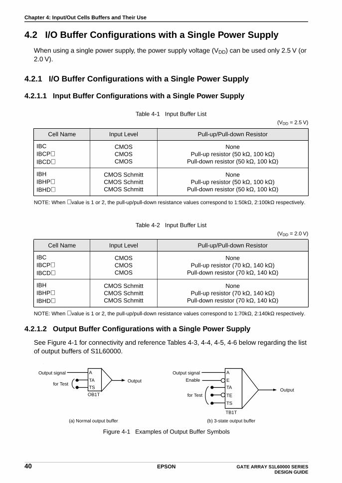
Chapter 4: Input/Out Cells Buffers and Their Use
4.2 I/O Buffer Configurations with a Single Power Supply
When using a single power supply, the power supply voltage (VDD) can be used only 2.5 V (or 2.0 V).
4.2.1 I/O Buffer Configurations with a Single Power Supply
4.2.1.1 Input Buffer Configurations with a Single Power Supply
NOTE: When ∗ value is 1 or 2, the pull-up/pull-down resistance values correspond to 1:50kΩ, 2:100kΩ respectively.
NOTE: When ∗ value is 1 or 2, the pull-up/pull-down resistance values correspond to 1:70kΩ, 2:140kΩ respectively.
4.2.1.2 Output Buffer Configurations with a Single Power Supply
See Figure 4-1 for connectivity and reference Tables 4-3, 4-4, 4-5, 4-6 below regarding the list of output buffers of S1L60000.
-
Figure 4-1 Examples of Output Buffer Symbols
Table 4-1 Input Buffer List(VDD = 2.5 V)
Cell Name Input Level Pull-up/Pull-down Resistor
IBCIBCP∗IBCD∗
CMOSCMOSCMOS
NonePull-up resistor (50 kΩ, 100 kΩ)
Pull-down resistor (50 kΩ, 100 kΩ)
IBHIBHP∗IBHD∗
CMOS SchmittCMOS SchmittCMOS Schmitt
NonePull-up resistor (50 kΩ, 100 kΩ)
Pull-down resistor (50 kΩ, 100 kΩ)
Table 4-2 Input Buffer List(VDD = 2.0 V)
Cell Name Input Level Pull-up/Pull-down Resistor
IBCIBCP∗IBCD∗
CMOSCMOSCMOS
NonePull-up resistor (70 kΩ, 140 kΩ)
Pull-down resistor (70 kΩ, 140 kΩ)
IBHIBHP∗IBHD∗
CMOS SchmittCMOS SchmittCMOS Schmitt
NonePull-up resistor (70 kΩ, 140 kΩ)
Pull-down resistor (70 kΩ, 140 kΩ)
OB1T
A
TA
TSfor Test
Output signal
TB1T
A
E
TA OutputTE
TS
Enable
(a) Normal output buffer (b) 3-state output buffer
for Test
Output signal
Output
40 EPSON GATE ARRAY S1L60000 SERIES DESIGN GUIDE
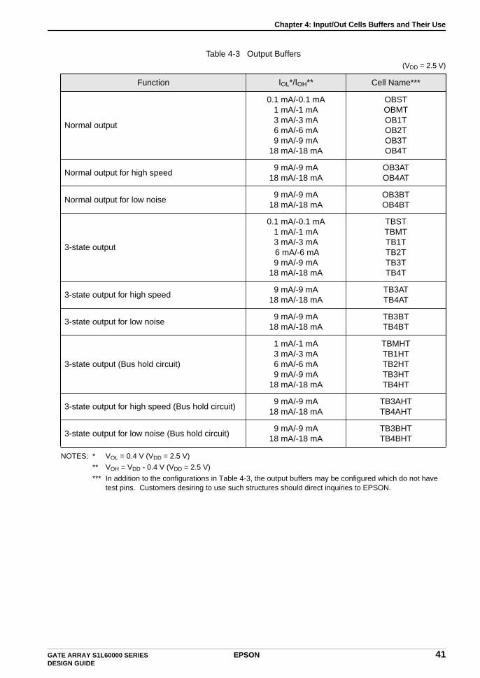
Chapter 4: Input/Out Cells Buffers and Their Use
NOTES: * VOL = 0.4 V (VDD = 2.5 V)
** VOH = VDD - 0.4 V (VDD = 2.5 V)
*** In addition to the configurations in Table 4-3, the output buffers may be configured which do not have test pins. Customers desiring to use such structures should direct inquiries to EPSON.
Table 4-3 Output Buffers (VDD = 2.5 V)
Function IOL*/IOH** Cell Name***
Normal output
0.1 mA/-0.1 mA1 mA/-1 mA3 mA/-3 mA6 mA/-6 mA9 mA/-9 mA
18 mA/-18 mA
OBSTOBMTOB1TOB2TOB3TOB4T
Normal output for high speed9 mA/-9 mA
18 mA/-18 mAOB3ATOB4AT
Normal output for low noise9 mA/-9 mA
18 mA/-18 mAOB3BTOB4BT
3-state output
0.1 mA/-0.1 mA1 mA/-1 mA3 mA/-3 mA 6 mA/-6 mA9 mA/-9 mA
18 mA/-18 mA
TBSTTBMTTB1TTB2TTB3TTB4T
3-state output for high speed9 mA/-9 mA
18 mA/-18 mATB3ATTB4AT
3-state output for low noise9 mA/-9 mA
18 mA/-18 mATB3BTTB4BT
3-state output (Bus hold circuit)
1 mA/-1 mA3 mA/-3 mA6 mA/-6 mA9 mA/-9 mA
18 mA/-18 mA
TBMHTTB1HTTB2HTTB3HTTB4HT
3-state output for high speed (Bus hold circuit)9 mA/-9 mA
18 mA/-18 mATB3AHTTB4AHT
3-state output for low noise (Bus hold circuit)9 mA/-9 mA
18 mA/-18 mATB3BHTTB4BHT
GATE ARRAY S1L60000 SERIES EPSON 41DESIGN GUIDE
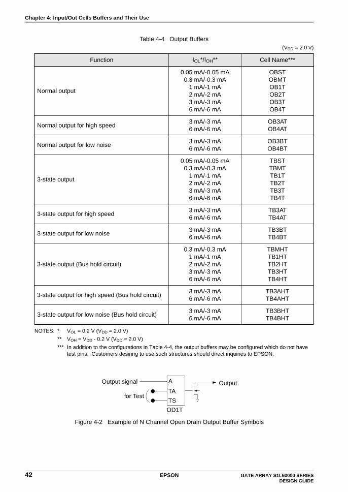
Chapter 4: Input/Out Cells Buffers and Their Use
NOTES: * VOL = 0.2 V (VDD = 2.0 V)
** VOH = VDD - 0.2 V (VDD = 2.0 V)
*** In addition to the configurations in Table 4-4, the output buffers may be configured which do not have test pins. Customers desiring to use such structures should direct inquiries to EPSON.
Figure 4-2 Example of N Channel Open Drain Output Buffer Symbols
Table 4-4 Output Buffers (VDD = 2.0 V)
Function IOL*/IOH** Cell Name***
Normal output
0.05 mA/-0.05 mA0.3 mA/-0.3 mA
1 mA/-1 mA2 mA/-2 mA3 mA/-3 mA6 mA/-6 mA
OBSTOBMTOB1TOB2TOB3TOB4T
Normal output for high speed3 mA/-3 mA6 mA/-6 mA
OB3ATOB4AT
Normal output for low noise3 mA/-3 mA6 mA/-6 mA
OB3BTOB4BT
3-state output
0.05 mA/-0.05 mA0.3 mA/-0.3 mA
1 mA/-1 mA2 mA/-2 mA3 mA/-3 mA6 mA/-6 mA
TBSTTBMTTB1TTB2TTB3TTB4T
3-state output for high speed3 mA/-3 mA6 mA/-6 mA
TB3ATTB4AT
3-state output for low noise3 mA/-3 mA6 mA/-6 mA
TB3BTTB4BT
3-state output (Bus hold circuit)
0.3 mA/-0.3 mA1 mA/-1 mA2 mA/-2 mA3 mA/-3 mA6 mA/-6 mA
TBMHTTB1HTTB2HTTB3HTTB4HT
3-state output for high speed (Bus hold circuit)3 mA/-3 mA6 mA/-6 mA
TB3AHTTB4AHT
3-state output for low noise (Bus hold circuit)3 mA/-3 mA6 mA/-6 mA
TB3BHTTB4BHT
OD1T
A
TA
TSfor Test
Output signal Output
42 EPSON GATE ARRAY S1L60000 SERIES DESIGN GUIDE

Chapter 4: Input/Out Cells Buffers and Their Use
NOTES: * VOL = 0.4 V (VDD = 2.5 V)
** In addition to the configurations in Table 4-5, N channel open drain output buffers may be configured which do not have test pins.Customers desiring to use such structures should direct inquiries to EPSON.
NOTES: * VOL = 0.2 V (VDD = 2.0 V)
** In addition to the configurations in Table 4-6, N channel open drain output buffers may be configured which do not have test pins.Customers desiring to use such structures should direct inquiries to EPSON.
4.2.1.3 Bi-directional Buffer Configurations with a Single Power Supply
The bi-directional buffers list of S1L60000 are shown in the Tables 4-7, 4-8, 4-9 and 4-10.
Figure 4-3 Example of Bi-directional Buffer Symbols
Table 4-5 N channel Open Drain Output Buffers (VDD = 2.5 V)
Function IOL*/IOH Cell Name**
Normal output
3 mA6 mA9 mA
18 mA
OD1TOD2TOD3TOD4T
Table 4-6 N channel Open Drain Output Buffers (VDD = 2.0 V)
Function IOL*/IOH Cell Name**
Normal output
1 mA2 mA3 mA6 mA
OD1TOD2TOD3TOD4T
BC1T
A
E
TA
for Test
Output signal
Bi-directionalTE
TS
Enable
Input signal
GATE ARRAY S1L60000 SERIES EPSON 43DESIGN GUIDE
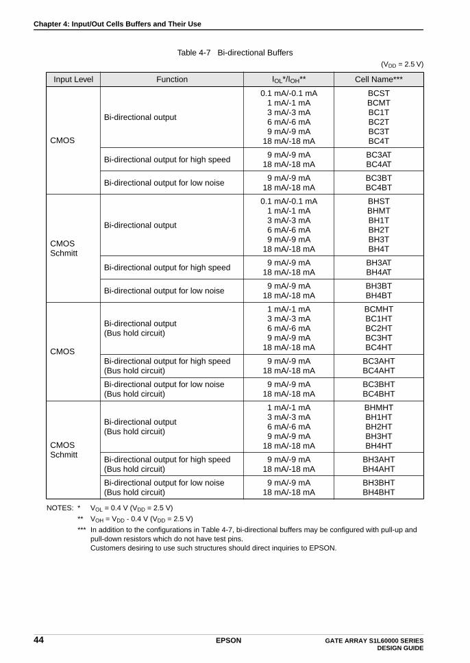
Chapter 4: Input/Out Cells Buffers and Their Use
NOTES: * VOL = 0.4 V (VDD = 2.5 V)
** VOH = VDD - 0.4 V (VDD = 2.5 V)
*** In addition to the configurations in Table 4-7, bi-directional buffers may be configured with pull-up and pull-down resistors which do not have test pins.Customers desiring to use such structures should direct inquiries to EPSON.
Table 4-7 Bi-directional Buffers (VDD = 2.5 V)
Input Level Function IOL*/IOH** Cell Name***
CMOS
Bi-directional output
0.1 mA/-0.1 mA1 mA/-1 mA3 mA/-3 mA6 mA/-6 mA9 mA/-9 mA
18 mA/-18 mA
BCSTBCMTBC1TBC2TBC3TBC4T
Bi-directional output for high speed9 mA/-9 mA
18 mA/-18 mABC3ATBC4AT
Bi-directional output for low noise9 mA/-9 mA
18 mA/-18 mABC3BTBC4BT
CMOS Schmitt
Bi-directional output
0.1 mA/-0.1 mA1 mA/-1 mA3 mA/-3 mA6 mA/-6 mA9 mA/-9 mA
18 mA/-18 mA
BHSTBHMTBH1TBH2TBH3TBH4T
Bi-directional output for high speed9 mA/-9 mA
18 mA/-18 mABH3ATBH4AT
Bi-directional output for low noise9 mA/-9 mA
18 mA/-18 mABH3BTBH4BT
CMOS
Bi-directional output (Bus hold circuit)
1 mA/-1 mA3 mA/-3 mA6 mA/-6 mA9 mA/-9 mA
18 mA/-18 mA
BCMHTBC1HTBC2HTBC3HTBC4HT
Bi-directional output for high speed(Bus hold circuit)
9 mA/-9 mA18 mA/-18 mA
BC3AHTBC4AHT
Bi-directional output for low noise(Bus hold circuit)
9 mA/-9 mA18 mA/-18 mA
BC3BHTBC4BHT
CMOSSchmitt
Bi-directional output (Bus hold circuit)
1 mA/-1 mA3 mA/-3 mA6 mA/-6 mA9 mA/-9 mA
18 mA/-18 mA
BHMHTBH1HTBH2HTBH3HTBH4HT
Bi-directional output for high speed(Bus hold circuit)
9 mA/-9 mA18 mA/-18 mA
BH3AHTBH4AHT
Bi-directional output for low noise(Bus hold circuit)
9 mA/-9 mA18 mA/-18 mA
BH3BHTBH4BHT
44 EPSON GATE ARRAY S1L60000 SERIES DESIGN GUIDE
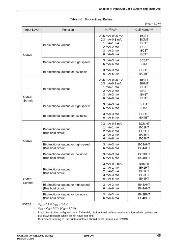
Chapter 4: Input/Out Cells Buffers and Their Use
NOTES: * VOL = 0.2 V (VDD = 2.0 V)
** VOH = VDD - 0.2 V (VDD = 2.0 V)
*** In addition to the configurations in Table 4-8, bi-directional buffers may be configured with pull-up and pull-down resistors which do not have test pins. Customers desiring to use such structures should direct inquiries to EPSON.
Table 4-8 Bi-directional Buffers (VDD = 2.0 V)
Input Level Function IOL*/IOH** Cell Name***
CMOS
Bi-directional output
0.05 mA/-0.05 mA0.3 mA/-0.3 mA
1 mA/-1 mA2 mA/-2 mA3 mA/-3 mA6 mA/-6 mA
BCSTBCMTBC1TBC2TBC3TBC4T
Bi-directional output for high speed3 mA/-3 mA6 mA/-6 mA
BC3ATBC4AT
Bi-directional output for low noise3 mA/-3 mA6 mA/-6 mA
BC3BTBC4BT
CMOS Schmitt
Bi-directional output
0.05 mA/-0.05 mA0.3 mA/-0.3 mA
1 mA/-1 mA2 mA/-2 mA3 mA/-3 mA6 mA/-6 mA
BHSTBHMTBH1TBH2TBH3TBH4T
Bi-directional output for high speed3 mA/-3 mA6 mA/-6 mA
BH3ATBH4AT
Bi-directional output for low noise3 mA/-3 mA6 mA/-6 mA
BH3BTBH4BT
CMOS
Bi-directional output (Bus hold circuit)
0.3 mA/-0.3 mA1 mA/-1 mA2 mA/-2 mA3 mA/-3 mA6 mA/-6 mA
BCMHTBC1HTBC2HTBC3HTBC4HT
Bi-directional output for high speed(Bus hold circuit)
3 mA/-3 mA6 mA/-6 mA
BC3AHTBC4AHT
Bi-directional output for low noise(Bus hold circuit)
3 mA/-3 mA6 mA/-6 mA
BC3BHTBC4BHT
CMOS Schmitt
Bi-directional output (Bus hold circuit)
0.3 mA/-0.3 mA1 mA/-1 mA2 mA/-2 mA3 mA/-3 mA6 mA/-6 mA
BHMHTBH1HTBH2HTBH3HTBH4HT
Bi-directional output for high speed(Bus hold circuit)
3 mA/-3 mA6 mA/-6 mA
BH3AHTBH4AHT
Bi-directional output for low noise (Bus hold circuit)
3 mA/-3 mA6 mA/-6 mA
BH3BHTBH4BHT
GATE ARRAY S1L60000 SERIES EPSON 45DESIGN GUIDE
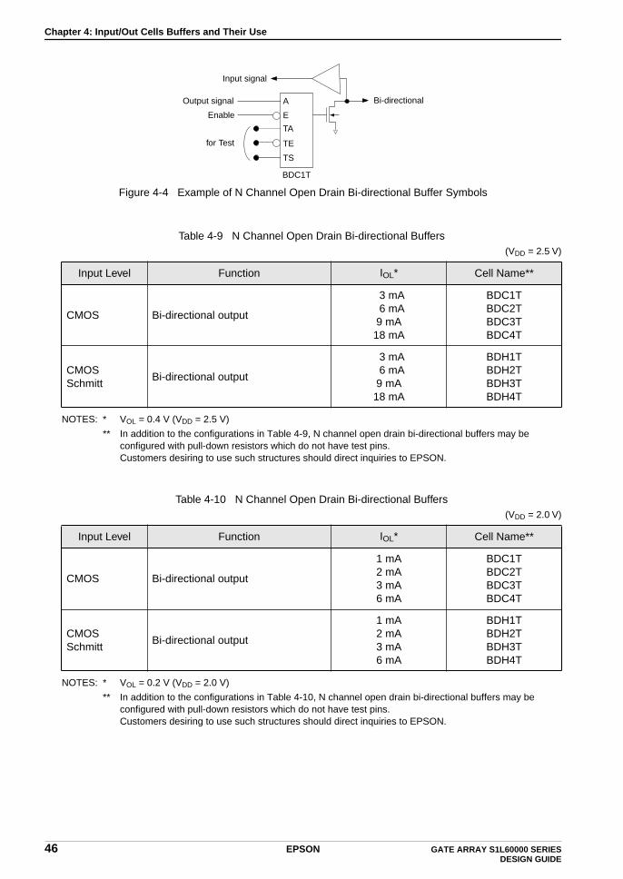
Chapter 4: Input/Out Cells Buffers and Their Use
Figure 4-4 Example of N Channel Open Drain Bi-directional Buffer Symbols
NOTES: * VOL = 0.4 V (VDD = 2.5 V)
** In addition to the configurations in Table 4-9, N channel open drain bi-directional buffers may be configured with pull-down resistors which do not have test pins.Customers desiring to use such structures should direct inquiries to EPSON.
NOTES: * VOL = 0.2 V (VDD = 2.0 V)
** In addition to the configurations in Table 4-10, N channel open drain bi-directional buffers may be configured with pull-down resistors which do not have test pins.Customers desiring to use such structures should direct inquiries to EPSON.
Table 4-9 N Channel Open Drain Bi-directional Buffers (VDD = 2.5 V)
Input Level Function IOL* Cell Name**
CMOS Bi-directional output
3 mA 6 mA9 mA
18 mA
BDC1TBDC2TBDC3TBDC4T
CMOS Schmitt
Bi-directional output
3 mA 6 mA9 mA
18 mA
BDH1TBDH2TBDH3TBDH4T
Table 4-10 N Channel Open Drain Bi-directional Buffers (VDD = 2.0 V)
Input Level Function IOL* Cell Name**
CMOS Bi-directional output
1 mA2 mA3 mA6 mA
BDC1TBDC2TBDC3TBDC4T
CMOS Schmitt
Bi-directional output
1 mA2 mA3 mA6 mA
BDH1TBDH2TBDH3TBDH4T
BDC1T
A
E
TA
for Test
Output signal Bi-directional
TE
TS
Enable
Input signal
46 EPSON GATE ARRAY S1L60000 SERIES DESIGN GUIDE
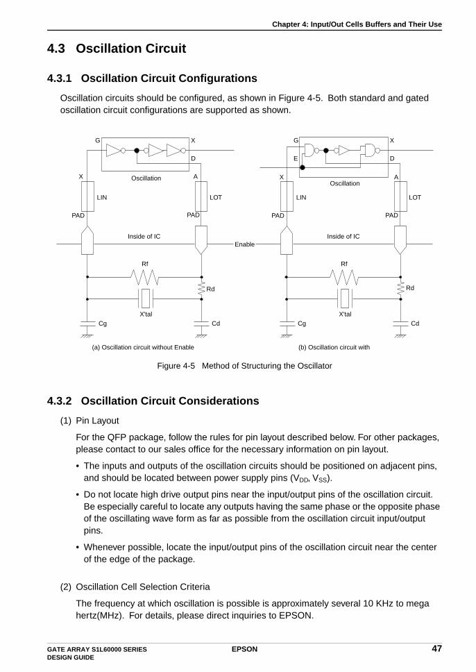
Chapter 4: Input/Out Cells Buffers and Their Use
4.3 Oscillation Circuit
4.3.1 Oscillation Circuit Configurations
Oscillation circuits should be configured, as shown in Figure 4-5. Both standard and gated oscillation circuit configurations are supported as shown.
Figure 4-5 Method of Structuring the Oscillator
4.3.2 Oscillation Circuit Considerations
(1) Pin Layout
For the QFP package, follow the rules for pin layout described below. For other packages, please contact to our sales office for the necessary information on pin layout.
• The inputs and outputs of the oscillation circuits should be positioned on adjacent pins, and should be located between power supply pins (VDD, VSS).
• Do not locate high drive output pins near the input/output pins of the oscillation circuit. Be especially careful to locate any outputs having the same phase or the opposite phase of the oscillating wave form as far as possible from the oscillation circuit input/output pins.
• Whenever possible, locate the input/output pins of the oscillation circuit near the center of the edge of the package.
(2) Oscillation Cell Selection Criteria
The frequency at which oscillation is possible is approximately several 10 KHz to mega hertz(MHz). For details, please direct inquiries to EPSON.
LIN LOT LIN LOT
G X
D
G X
DE
Cg Cd
Rf
Rd
X'talCg Cd
Rf
Rd
X'tal
X A
PADPAD
X A
PADPAD
OscillationOscillation
Inside of IC Inside of IC
(a) Oscillation circuit without Enable (b) Oscillation circuit with
Enable
GATE ARRAY S1L60000 SERIES EPSON 47DESIGN GUIDE
Chapter 4: Input/Out Cells Buffers and Their Use
(3) Selecting the Values for the Resistors and Capacitors to be Attached
The characteristics of oscillation depends on the capacitive and resistive biasing elements (IC, X’tal, Rf, Rd, Cg, Cd, boards). Because of this, the capacitive and resistive values must be adjusted, depending on the crystal which will be used on the actual board. Consequently, the optimal values should be chosen through spending adequate time evaluating available engineering samples.
(4) Assurance Levels
EPSON is unable to guarantee the function or characteristics of the oscillation. EPSON can warrantee only the oscillation cell. Because of this, it is necessary for the customer to spend adequate time evaluating the engineering samples in terms of their oscillation characteristics.
(5) Structuring Oscillation Circuits for Dual Power Supplies
The structure of oscillation circuits for dual power supplies is essentially no different than the structure for single power supplies. The oscillation circuit operates on the LVDD system. Moreover, for input/output cells LIN and LOT, use LLIN and LLOT, which each have the prefix Low to denote operation using LVDD.
4.4 Gated I/O Cells
4.4.1 Overview of Gated Cells
Gated I/O cells can use the input of pins to be floated or Hi-Z state, in other words, without using the pull up or down resistor that is impossible as usual. Also, if they are used, the power source of the high voltage side (HVDD) designed at the dual power sources circuit can be cut off. There are two types; one is cut off at the High level of the control signal and the other at the Low level of the control signal, so it is selectable depending on the circuit design.
4.4.2 Feature of Gated I/O Cell
(1) There is no limitation on how many Gated cells are used and arranged, so they can be used to correspond to need to design a logic circuit.
(2) The power source of the high voltage side (HVDD) designed at the dual power source can be cut off. Before you cut off the power to the high-voltage side (HVDD), first contact EPSON’s marketing division, as a special procedure is required in this case.
(3) The gated I/O cells can use the input of the cells to be floated or Hi-Z state, in other words without using the pull up or down resistor.
(4) The input levels of dual power source circuit gated I/O cells correspond to CMOS (LVDD).
(5) There are two types; one is cut off at a High level control signal and the other at a Low level control signal.
(6) The gated cells of the S1L60000 series are composed by the complete CMOS structure, so they can operate at low power.
48 EPSON GATE ARRAY S1L60000 SERIES DESIGN GUIDE

Chapter 4: Input/Out Cells Buffers and Their Use
4.4.3 Notes on Using Gated Cell
(1) When the input of cells are set to Hi-Z state by using the gated I/O cells, the cut off of power source must be operated by using the control of the gated I/O cells before the input of cells set to Hi-Z state. If this operation is not executed and the input of cells is set to Hi-Z state, large current flows to the input cell in the same manner as normal cells and the LSI elements may be destroyed. Otherwise, when the input cells are set to Hi-Z state and a connecting operation is executed by using the control of the gated cell, a large current flows to the input cell in the same manner as for normal cells and the LSI elements may be destroyed. In this case, EPSON does not guarantee the logic levels in the internal device.
(2) When the power source of high voltage side (HVDD) is cut off by using the gated I/O cells, the same process as in (1) needs to be carried out. Also, in this case, EPSON does not guarantee the logic levels in the internal device. Before you cut off the power to the high-voltage side (HVDD), first contact EPSON’s marketing division, as a special procedure is also required in this case.
*1:The value at VDD = 2.5 V
*1: The value at HVDD = 3.3 V
Table 4-11 Gated Input Cell List (VDD = 2.5 V, 2.0 V)
Drain Type Input LevelWithout Resistor
Pull Down *1 Pull Up *1
50 kΩ 100 kΩ 50 kΩ 100 kΩ
Normal CMOSAND IBA IBAD1 IBAD2 IBAP1 IBAP2
OR IBO IBOD1 IBOD2 IBOP1 IBOP2
Table 4-12 Gated Input Cell List (HVDD = 3.3 V)
Drain Type Input LevelWithout Resistor
Pull Down *1 Pull Up *1
60 kΩ 120 kΩ 60 kΩ 120 kΩ
Normal CMOSAND HIBA HIBAD1 HIBAD2 HIBAP1 HIBAP2
OR HIBO HIBOD1 HIBOD2 HIBOP1 HIBOP2
GATE ARRAY S1L60000 SERIES EPSON 49DESIGN GUIDE

Chapter 4: Input/Out Cells Buffers and Their Use
*1: The value at VDD = 2.5 V
*2: In addition to the configurations in Table 4-13, the gated bi-directional buffers may be configured which do not have test pins. Customers desiring to use such structures should direct inquiries to EPSON.
*1: The value at VDD = 2.5 V
*2: In addition to the configurations in Table 4-14, the gated bi-directional buffers may be configured which do not have test pins. Customers desiring to use such structures should direct inquiries to EPSON.
Table 4-13 Gated Bi-directional Cell List (AND Type, VDD = 2.5 V, 2.0 V)
Input Level
Drain Type
Test Function*2
Output Latch
FunctionSpeed
Output Current(mA)*1
Without Resistor
Pull Down *1 Pull Up *1
50 kΩ 100 kΩ 50 kΩ 100 kΩ
CMOS Normal ExistNon-exist
Normal
-3/3 BA1T BA1D1T BA1D2T BA1P1T BA1P2T
-6/6 BA2T BA2D1T BA2D2T BA2P1T BA2P2T
-9/9 BA3T BA3D1T BA3D2T BA3P1T BA3P2T
-18/18 BA4T BA4D1T BA4D2T BA4P1T BA4P2T
High Speed
-9/9 BA3AT BA3AD1T BA3AD2T BA3AP1T BA3AP2T
-18/18 BA4AT BA4AD1T BA4AD2T BA4AP1T BA4AP2T
Low Noise
-9/9 BA3BT BA3BD1T BA3BD2T BA3BP1T BA3BP2T
-18/18 BA4BT BA4BD1T BA4BD2T BA4BP1T BA4BP2T
Table 4-14 Gated Bi-directional Cell List (OR Type, VDD = 2.5 V, 2.0 V)
Input Level
Drain Type
Test Function*2
Output Latch
FunctionSpeed
Output Current(mA)*1
Without Resistor
Pull Down *1 Pull Up *1
50 kΩ 100 kΩ 50 kΩ 100 kΩ
CMOS Normal ExistNon-exist
Normal
-3/3 BO1T BO1D1T BO1D2T BO1P1T BO1P2T
-6/6 BO2T BO2D1T BO2D2T BO2P1T BO2P2T
-9/9 BO3T BO3D1T BO3D2T BO3P1T BO3P2T
-18/18 BO4T BO4D1T BO4D2T BO4P1T BO4P2T
High Speed
-9/9 BO3AT BO3AD1T BO3AD2T BO3AP1T BO3AP2T
-18/18 BO4AT BO4AD1T BO4AD2T BO4AP1T BO4AP2T
Low Noise
-9/9 BO3BT BO3BD1T BO3BD2T BO3BP1T BO3BP2T
-18/18 BO4BT BO4BD1T BO4BD2T BO4BP1T BO4BP2T
50 EPSON GATE ARRAY S1L60000 SERIES DESIGN GUIDE
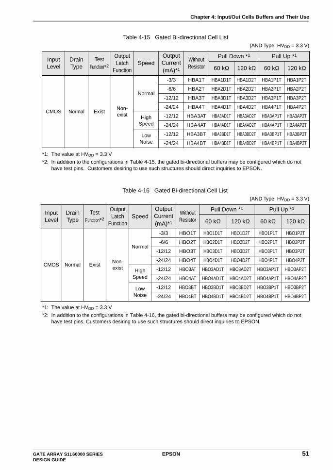
Chapter 4: Input/Out Cells Buffers and Their Use
*1: The value at HVDD = 3.3 V
*2: In addition to the configurations in Table 4-15, the gated bi-directional buffers may be configured which do not have test pins. Customers desiring to use such structures should direct inquiries to EPSON.
*1: The value at HVDD = 3.3 V
*2: In addition to the configurations in Table 4-16, the gated bi-directional buffers may be configured which do not have test pins. Customers desiring to use such structures should direct inquiries to EPSON.
Table 4-15 Gated Bi-directional Cell List (AND Type, HVDD = 3.3 V)
Input Level
Drain Type
Test Function*2
Output Latch
FunctionSpeed
Output Current(mA)*1
Without Resistor
Pull Down *1 Pull Up *1
60 kΩ 120 kΩ 60 kΩ 120 kΩ
CMOS Normal ExistNon-exist
Normal
-3/3 HBA1T HBA1D1T HBA1D2T HBA1P1T HBA1P2T
-6/6 HBA2T HBA2D1T HBA2D2T HBA2P1T HBA2P2T
-12/12 HBA3T HBA3D1T HBA3D2T HBA3P1T HBA3P2T
-24/24 HBA4T HBA4D1T HBA4D2T HBA4P1T HBA4P2T
High Speed
-12/12 HBA3AT HBA3AD1T HBA3AD2T HBA3AP1T HBA3AP2T
-24/24 HBA4AT HBA4AD1T HBA4AD2T HBA4AP1T HBA4AP2T
Low Noise
-12/12 HBA3BT HBA3BD1T HBA3BD2T HBA3BP1T HBA3BP2T
-24/24 HBA4BT HBA4BD1T HBA4BD2T HBA4BP1T HBA4BP2T
Table 4-16 Gated Bi-directional Cell List (AND Type, HVDD = 3.3 V)
Input Level
Drain Type
Test Function*2
Output Latch
FunctionSpeed
Output Current(mA)*1
Without Resistor
Pull Down *1 Pull Up *1
60 kΩ 120 kΩ 60 kΩ 120 kΩ
CMOS Normal ExistNon-exist
Normal
-3/3 HBO1T HBO1D1T HBO1D2T HBO1P1T HBO1P2T
-6/6 HBO2T HBO2D1T HBO2D2T HBO2P1T HBO2P2T
-12/12 HBO3T HBO3D1T HBO3D2T HBO3P1T HBO3P2T
-24/24 HBO4T HBO4D1T HBO4D2T HBO4P1T HBO4P2T
High Speed
-12/12 HBO3AT HBO3AD1T HBO3AD2T HBO3AP1T HBO3AP2T
-24/24 HBO4AT HBO4AD1T HBO4AD2T HBO4AP1T HBO4AP2T
Low Noise
-12/12 HBO3BT HBO3BD1T HBO3BD2T HBO3BP1T HBO3BP2T
-24/24 HBO4BT HBO4BD1T HBO4BD2T HBO4BP1T HBO4BP2T
GATE ARRAY S1L60000 SERIES EPSON 51DESIGN GUIDE

Chapter 4: Input/Out Cells Buffers and Their Use
4.5 Fail Safe Cell
4.5.1 Overview of Fail Safe Cell
The Fail Safe cell of the S1L60000 series can interface to a signal that has more power voltage than at the bi-directional pin designed to use the single power source without setting the special power source to interface. Therefore, the LSI does not need to set two power sources, of which one is used for operation and the other for interface. Furthermore, the same level signal as the power source for operation can be interfaced without changing the circuit, so the logic circuit can be designed more freely.
4.5.2 Feature of Fail Safe Cell
(1) There is no limitation on how many Fail Safe cells are used and arranged, so they can be used to correspond to the need to design a logic circuit.
(2) The Fail Safe cells of the S1L60000 series can interface to an external signal that has more power voltage than that designed for the single power source without setting a special power source for the interface.
(3) The input levels of the S1L60000 series Fail Safe cells correspond to CMOS and CMOS Schmitt.
(4) The Fail Safe cells of the S1L60000 series are composed by a complete CMOS structure, so they can operate at low power.
4.5.3 Notes on Using Fail Safe Cell
(1) The Fail Safe cells now released set the output pins High-Z such that DC current never flows at the input mode, even though they are inputted a higher power voltage signal than the designed power voltage. However, when they output at High level on the output mode and are inputted a higher power voltage signal than the designed power voltage, DC current may flow to the LSI as usual. For example, when the Fail Safe cells produced by EPSON output at High level (2.5 V), another device indicates output at High level (3.3 V) at the same time. Also, this other device includes pull up resistor.
(2) Note that the Fail Safe cell can be impressed only signal voltage that is less than the absolute maximum ratings, although they can receive a signal voltage that is higher than the LSI operation voltage.
*1: The value at VDD = 2.5 V
Table 4-17 Fail Safe Input Buffer List (VDD = 2.5 V, 2.0 V)
Drain Type Input LevelWithout Resistor
Pull Down*1 Pull Up*1
50 kΩ 100 kΩ 50 kΩ 100 kΩ
Fail SafeCMOS — — — IBBP1 IBBP2
CMOS-Schmitt — — — IBGP1 IBGP2
52 EPSON GATE ARRAY S1L60000 SERIES DESIGN GUIDE
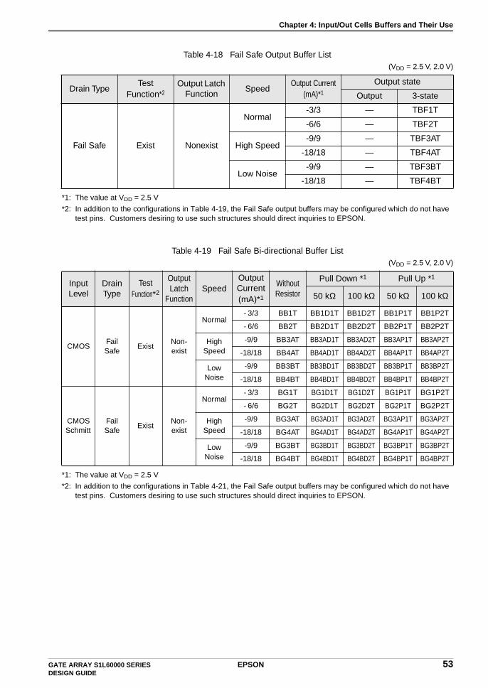
Chapter 4: Input/Out Cells Buffers and Their Use
*1: The value at VDD = 2.5 V
*2: In addition to the configurations in Table 4-19, the Fail Safe output buffers may be configured which do not have test pins. Customers desiring to use such structures should direct inquiries to EPSON.
*1: The value at VDD = 2.5 V
*2: In addition to the configurations in Table 4-21, the Fail Safe output buffers may be configured which do not have test pins. Customers desiring to use such structures should direct inquiries to EPSON.
Table 4-18 Fail Safe Output Buffer List (VDD = 2.5 V, 2.0 V)
Drain TypeTest
Function*2Output Latch
FunctionSpeed
Output Current(mA)*1
Output state
Output 3-state
Fail Safe Exist Nonexist
Normal-3/3 — TBF1T
-6/6 — TBF2T
High Speed-9/9 — TBF3AT
-18/18 — TBF4AT
Low Noise-9/9 — TBF3BT
-18/18 — TBF4BT
Table 4-19 Fail Safe Bi-directional Buffer List (VDD = 2.5 V, 2.0 V)
Input Level
Drain Type
Test Function*2
Output Latch
FunctionSpeed
Output Current(mA)*1
Without Resistor
Pull Down *1 Pull Up *1
50 kΩ 100 kΩ 50 kΩ 100 kΩ
CMOSFail Safe
ExistNon-exist
Normal- 3/3 BB1T BB1D1T BB1D2T BB1P1T BB1P2T
- 6/6 BB2T BB2D1T BB2D2T BB2P1T BB2P2T
High Speed
-9/9 BB3AT BB3AD1T BB3AD2T BB3AP1T BB3AP2T
-18/18 BB4AT BB4AD1T BB4AD2T BB4AP1T BB4AP2T
Low Noise
-9/9 BB3BT BB3BD1T BB3BD2T BB3BP1T BB3BP2T
-18/18 BB4BT BB4BD1T BB4BD2T BB4BP1T BB4BP2T
CMOSSchmitt
Fail Safe
ExistNon-exist
Normal- 3/3 BG1T BG1D1T BG1D2T BG1P1T BG1P2T
- 6/6 BG2T BG2D1T BG2D2T BG2P1T BG2P2T
High Speed
-9/9 BG3AT BG3AD1T BG3AD2T BG3AP1T BG3AP2T
-18/18 BG4AT BG4AD1T BG4AD2T BG4AP1T BG4AP2T
Low Noise
-9/9 BG3BT BG3BD1T BG3BD2T BG3BP1T BG3BP2T
-18/18 BG4BT BG4BD1T BG4BD2T BG4BP1T BG4BP2T
GATE ARRAY S1L60000 SERIES EPSON 53DESIGN GUIDE
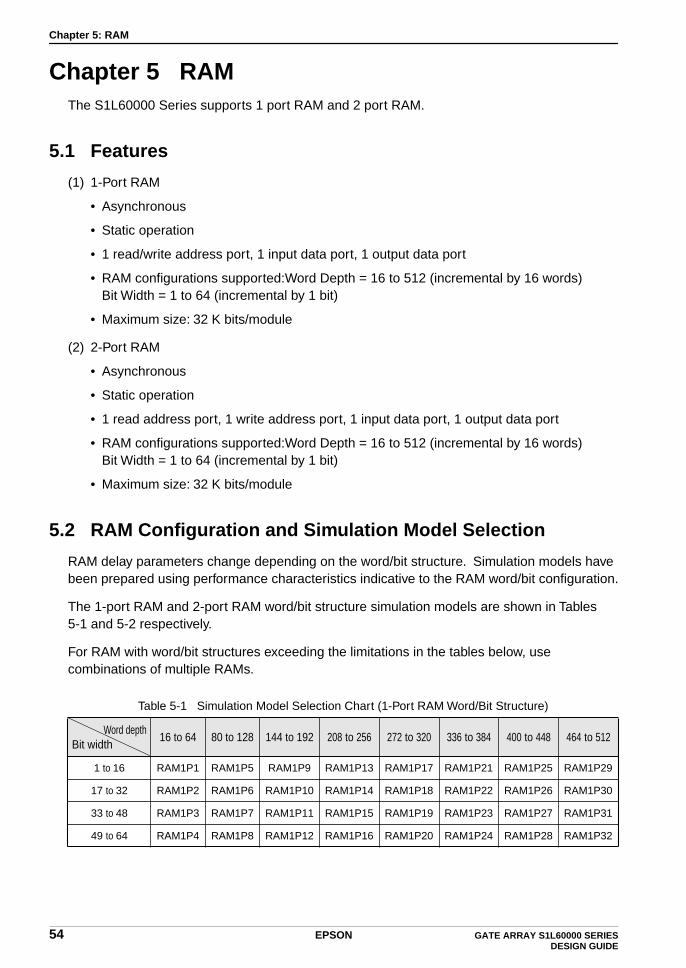
Chapter 5: RAM
Chapter 5 RAMThe S1L60000 Series supports 1 port RAM and 2 port RAM.
5.1 Features
(1) 1-Port RAM
• Asynchronous
• Static operation
• 1 read/write address port, 1 input data port, 1 output data port
• RAM configurations supported:Word Depth = 16 to 512 (incremental by 16 words)Bit Width = 1 to 64 (incremental by 1 bit)
• Maximum size: 32 K bits/module
(2) 2-Port RAM
• Asynchronous
• Static operation
• 1 read address port, 1 write address port, 1 input data port, 1 output data port
• RAM configurations supported:Word Depth = 16 to 512 (incremental by 16 words)Bit Width = 1 to 64 (incremental by 1 bit)
• Maximum size: 32 K bits/module
5.2 RAM Configuration and Simulation Model Selection
RAM delay parameters change depending on the word/bit structure. Simulation models have been prepared using performance characteristics indicative to the RAM word/bit configuration.
The 1-port RAM and 2-port RAM word/bit structure simulation models are shown in Tables 5-1 and 5-2 respectively.
For RAM with word/bit structures exceeding the limitations in the tables below, use combinations of multiple RAMs.
Table 5-1 Simulation Model Selection Chart (1-Port RAM Word/Bit Structure)
Word depthBit width
16 to 64 80 to 128 144 to 192 208 to 256 272 to 320 336 to 384 400 to 448 464 to 512
1 to 16 RAM1P1 RAM1P5 RAM1P9 RAM1P13 RAM1P17 RAM1P21 RAM1P25 RAM1P29
17 to 32 RAM1P2 RAM1P6 RAM1P10 RAM1P14 RAM1P18 RAM1P22 RAM1P26 RAM1P30
33 to 48 RAM1P3 RAM1P7 RAM1P11 RAM1P15 RAM1P19 RAM1P23 RAM1P27 RAM1P31
49 to 64 RAM1P4 RAM1P8 RAM1P12 RAM1P16 RAM1P20 RAM1P24 RAM1P28 RAM1P32
54 EPSON GATE ARRAY S1L60000 SERIES DESIGN GUIDE

Chapter 5: RAM
5.3 RAM Size
The X-direction size, Y-direction size, and number of BCs used in the RAM are calculated using the formulas below. The formulas below do not include the interconnect region contained in the RAM.
(1) 1-Port RAM
Size in the X direction:RX = 3 × Word/2 + 20Size in the Y direction:RY = 2 × Bit + 12 (16 ≤ word ≤ 256)RY = 2 × Bit + 13 (256 < word ≤ 512)Number of BCs: RAMBCS = RX × RY
(2) 2-Port RAM
Size in the X direction:RX = 3 × Word/2 + 20Size in the Y direction:RY = 2 × Bit + 15 (16 ≤ word ≤ 256)RY = 2 × Bit + 17 (256 < word ≤ 512)Number of BCs: RAMBCS = RX × RY
Table 5-2 Simulation Model Selection Chart (2-Port RAM Word/Bit Structure)
Word depthBit width
16 to 64 80 to 128 144 to 192 208 to 256 272 to 320 336 to 384 400 to 448 464 to 512
1 to 16 RAM2P1 RAM2P5 RAM2P9 RAM2P13 RAM2P17 RAM2P21 RAM2P25 RAM2P29
17 to 32 RAM2P2 RAM2P6 RAM2P10 RAM2P14 RAM2P18 RAM2P22 RAM2P26 RAM2P30
33 to 48 RAM2P3 RAM2P7 RAM2P11 RAM2P15 RAM2P19 RAM2P23 RAM2P27 RAM2P31
49 to 64 RAM2P4 RAM2P8 RAM2P12 RAM2P16 RAM2P20 RAM2P24 RAM2P28 RAM2P32
Table 5-3 An Example of the Structure of 1-Port RAM and Number of BCs
Bit widthWord depth
8 16 32 64
64 3248 (116 × 28) 5104 (116 × 44) 8816 (116 × 76) 16240 (116 × 140)
128 5936 (212 × 28) 9328 (212 × 44) 16112 (212 × 76) 29680 (212 × 140)
256 11312 (404 × 28) 17776 (404 × 44) 30704 (404 × 76) 56560 (404 × 140)
512 22852 (788 × 29) 35460 (788 × 45) 60676 (788 × 77) 111108 (788 × 141)
Table 5-4 An Example of the Structure of 2-Port RAM and Number of BCs
Bit widthWord depth
8 16 32 64
64 3596 (116 × 31) 5452 (116 × 47) 9164 (116 × 79) 16588 (116 × 143)
128 6572 (212 × 31) 9964 (212 × 47) 16748 (212 × 79) 30316 (212 × 143)
256 12524 (404 × 31) 18988 (404 × 47) 31916 (404 × 79) 57772 (404 × 143)
512 26004 (788 × 33) 38612 (788 × 49) 63828 (788 × 81) 114260 (788 × 145)
GATE ARRAY S1L60000 SERIES EPSON 55DESIGN GUIDE

Chapter 5: RAM
5.4 Investigating RAM Placement on Master Slice
When investigating RAM placement on a master slice, please insure that sufficient area is available in both the X direction (column) and the Y direction (row). When loading RAM onto a chip, it is necessary to insure that the capacity of the master exceeds the required RAM area in both the X and Y directions.
When multiple RAMs are used, RAM blocks are placed adjacent to each other either horizontally or vertically. The wiring areas around RAM are not included in the equation shown in the previous section. It is therefore not possible to determine the advantages and disadvantages of placing RAM on the master slice based on values obtained by simply adding RXSIZE and RYSIZE to the sizes in the X and Y directions, respectively. As shown in Figure 5-1, add the interconnecting area of Bit/2 BC (round up to the nearest whole number) to X direction and every 1 BC to the upper and lower of Y direction, then the regarding master slice selection should be decided to mount or not.
Please see Table 1-1 of Chapter 1 regarding the number of columns (X-direction) and number of rows (Y-direction).
For example, if four 256 word × 16 bit 1-port RAMs are required.
As shown in Figure 5-1, the total RAM layout area would be:
X direction: 412 BCsY direction: 184 BCs
Because of this,
S1L60093/60094 is (X, Y) = (605, 164) is impossible due to area constraints, however,S1L60173/60174 is (X, Y) = (795, 216) is possible.
See Section 2.5 of Chapter 2 pertaining to estimating the number of gates, which can be used for random logic.
Figure 5-1 Example of RAM Layout
256W×
16b RAM× 4
412
RAM (1)
RAM (2)
RAM (3)
RAM
(4)
184
404
44
46
46
46
4646
1
81
56 EPSON GATE ARRAY S1L60000 SERIES DESIGN GUIDE
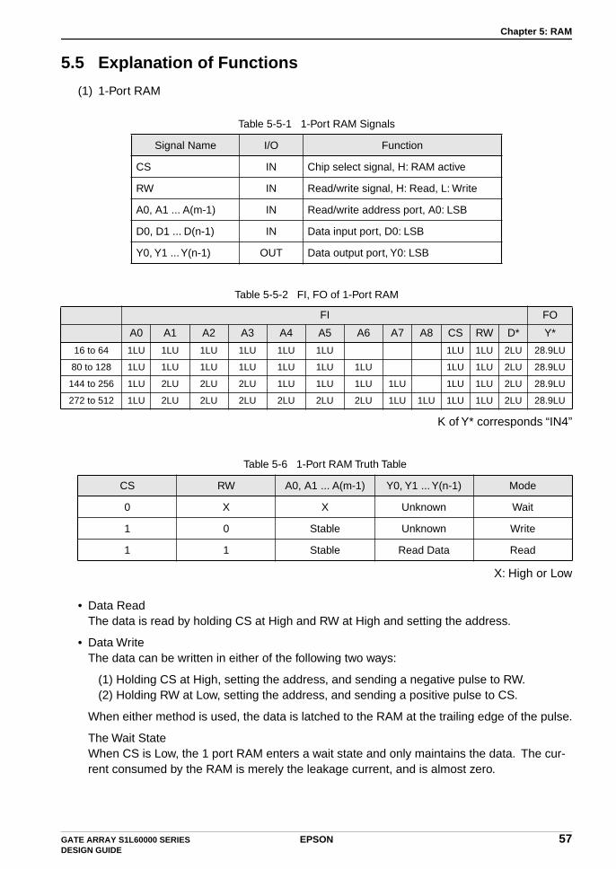
Chapter 5: RAM
5.5 Explanation of Functions
(1) 1-Port RAM
K of Y* corresponds “IN4”
X: High or Low
• Data ReadThe data is read by holding CS at High and RW at High and setting the address.
• Data WriteThe data can be written in either of the following two ways:
(1) Holding CS at High, setting the address, and sending a negative pulse to RW.(2) Holding RW at Low, setting the address, and sending a positive pulse to CS.
When either method is used, the data is latched to the RAM at the trailing edge of the pulse.
The Wait StateWhen CS is Low, the 1 port RAM enters a wait state and only maintains the data. The cur-rent consumed by the RAM is merely the leakage current, and is almost zero.
Table 5-5-1 1-Port RAM Signals
Signal Name I/O Function
CS IN Chip select signal, H: RAM active
RW IN Read/write signal, H: Read, L: Write
A0, A1 ... A(m-1) IN Read/write address port, A0: LSB
D0, D1 ... D(n-1) IN Data input port, D0: LSB
Y0, Y1 ... Y(n-1) OUT Data output port, Y0: LSB
Table 5-5-2 FI, FO of 1-Port RAM
FI FO
A0 A1 A2 A3 A4 A5 A6 A7 A8 CS RW D* Y*
16 to 64 1LU 1LU 1LU 1LU 1LU 1LU 1LU 1LU 2LU 28.9LU
80 to 128 1LU 1LU 1LU 1LU 1LU 1LU 1LU 1LU 1LU 2LU 28.9LU
144 to 256 1LU 2LU 2LU 2LU 1LU 1LU 1LU 1LU 1LU 1LU 2LU 28.9LU
272 to 512 1LU 2LU 2LU 2LU 2LU 2LU 2LU 1LU 1LU 1LU 1LU 2LU 28.9LU
Table 5-6 1-Port RAM Truth Table
CS RW A0, A1 ... A(m-1) Y0, Y1 ... Y(n-1) Mode
0 X X Unknown Wait
1 0 Stable Unknown Write
1 1 Stable Read Data Read
GATE ARRAY S1L60000 SERIES EPSON 57DESIGN GUIDE
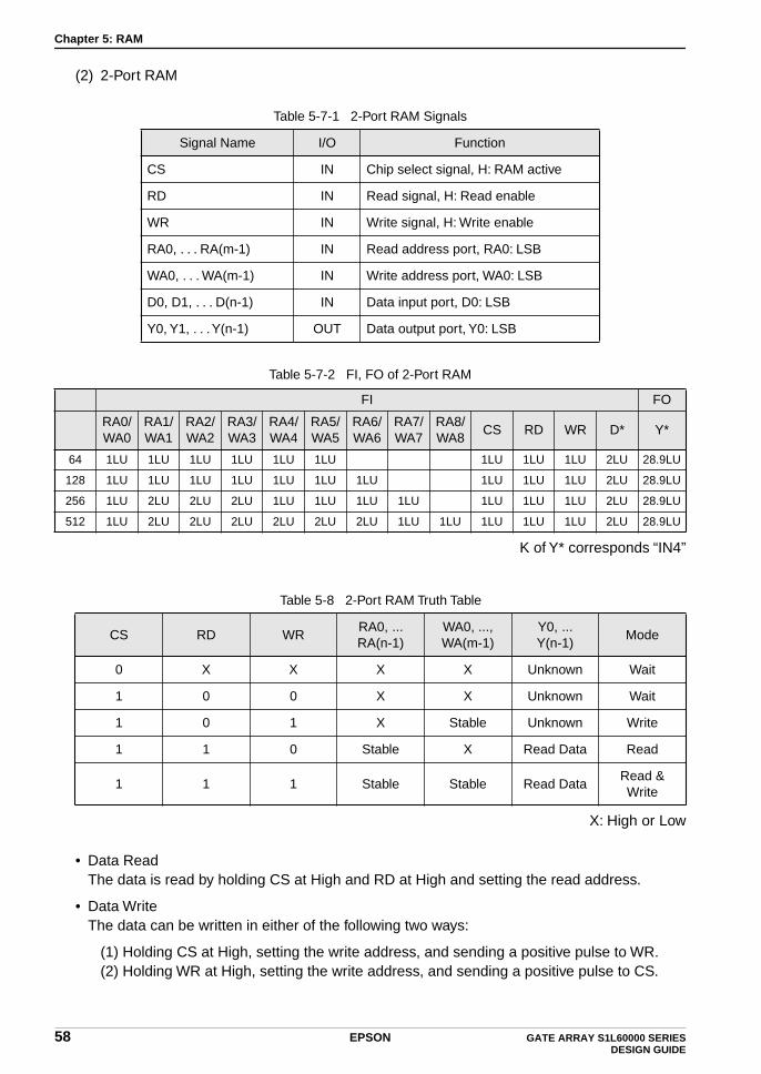
Chapter 5: RAM
(2) 2-Port RAM
K of Y* corresponds “IN4”
X: High or Low
• Data ReadThe data is read by holding CS at High and RD at High and setting the read address.
• Data WriteThe data can be written in either of the following two ways:
(1) Holding CS at High, setting the write address, and sending a positive pulse to WR.(2) Holding WR at High, setting the write address, and sending a positive pulse to CS.
Table 5-7-1 2-Port RAM Signals
Signal Name I/O Function
CS IN Chip select signal, H: RAM active
RD IN Read signal, H: Read enable
WR IN Write signal, H: Write enable
RA0, . . . RA(m-1) IN Read address port, RA0: LSB
WA0, . . . WA(m-1) IN Write address port, WA0: LSB
D0, D1, . . . D(n-1) IN Data input port, D0: LSB
Y0, Y1, . . . Y(n-1) OUT Data output port, Y0: LSB
Table 5-7-2 FI, FO of 2-Port RAM
FI FO
RA0/WA0
RA1/WA1
RA2/WA2
RA3/WA3
RA4/WA4
RA5/WA5
RA6/WA6
RA7/WA7
RA8/WA8
CS RD WR D* Y*
64 1LU 1LU 1LU 1LU 1LU 1LU 1LU 1LU 1LU 2LU 28.9LU
128 1LU 1LU 1LU 1LU 1LU 1LU 1LU 1LU 1LU 1LU 2LU 28.9LU
256 1LU 2LU 2LU 2LU 1LU 1LU 1LU 1LU 1LU 1LU 1LU 2LU 28.9LU
512 1LU 2LU 2LU 2LU 2LU 2LU 2LU 1LU 1LU 1LU 1LU 1LU 2LU 28.9LU
Table 5-8 2-Port RAM Truth Table
CS RD WRRA0, ... RA(n-1)
WA0, ..., WA(m-1)
Y0, ... Y(n-1)
Mode
0 X X X X Unknown Wait
1 0 0 X X Unknown Wait
1 0 1 X Stable Unknown Write
1 1 0 Stable X Read Data Read
1 1 1 Stable Stable Read DataRead & Write
58 EPSON GATE ARRAY S1L60000 SERIES DESIGN GUIDE

Chapter 5: RAM
• Data Read/WriteWhen reading is done at the same time as writing, it is possible by performing the respective methods simultaneously. However, these two operations cannot be performed simulta-neously on the same address. The read cycle access time described at Section 5.6 applies to data for which the writing has already been completed.
• The Wait StateThe 2 port RAM enters a wait state in either of the situations below, and does nothing but maintain its data. The current consumed by the RAM is merely the leakage current, and is almost 0.
(1) CS is Low.(2) CS is High, RD is Low, and WR is Low.
GATE ARRAY S1L60000 SERIES EPSON 59DESIGN GUIDE

Chapter 5: RAM
5.6 Delay Parameters
(1) 2.5 V Specifications (VDD = 2.3 to 2.7 V ; Ta = -40 to 85°C)
Table 5-9 1-Port/2-Port RAM Read Cycle (1/8)
Parameter SignalRAM1P1/RAM2P1 RAM1P2/RAM2P2 RAM1P3/RAM2P3 RAM1P4/RAM2P4
UnitMin. Max. Min. Max. Min. Max. Min. Max.
Read cycle tRC 4.605 — 5.239 — 5.519 — 6.203 —
ns
Address access time tACC — 4.605 — 5.239 — 5.519 — 6.203
CS access time tACS — 4.605 — 5.239 — 5.519 — 6.203
RW access time tARW — 4.605 — 5.239 — 5.519 — 6.203
CS active time tRCS 4.605 — 5.239 — 5.519 — 6.203 —
Output hold time after address change
tOH 0.093 — 0.153 — 0.212 — 0.272 —
Output hold time after CS disable
tOHCS 0.093 — 0.153 — 0.212 — 0.272 —
Output hold time after RW disable
tOHRW 0.093 — 0.153 — 0.212 — 0.272 —
Table 5-9 1-Port/2-Port RAM Read Cycle (2/8)
Parameter SignalRAM1P5/RAM2P5 RAM1P6/RAM2P6 RAM1P7/RAM2P7 RAM1P8/RAM2P8
UnitMin. Max. Min. Max. Min. Max. Min. Max.
Read cycle tRC 5.668 — 6.302 — 6.581 — 7.266 —
ns
Address access time tACC — 5.668 — 6.302 — 6.581 — 7.266
CS access time tACS — 5.668 — 6.302 — 6.581 — 7.266
RW access time tARW — 5.668 — 6.302 — 6.581 — 7.266
CS active time tRCS 5.668 — 6.302 — 6.581 — 7.266 —
Output hold time after address change
tOH 0.093 — 0.153 — 0.212 — 0.272 —
Output hold time after CS disable
tOHCS 0.093 — 0.153 — 0.212 — 0.272 —
Output hold time after RW disable
tOHRW 0.093 — 0.153 — 0.212 — 0.272 —
60 EPSON GATE ARRAY S1L60000 SERIES DESIGN GUIDE

Chapter 5: RAM
(1) 2.5 V Specifications (VDD = 2.3 to 2.7 V ; Ta = -40 to 85°C)
Table 5-9 1-Port/2-Port RAM Read Cycle (3/8)
Parameter SignalRAM1P9/RAM2P9 RAM1P10/RAM2P10 RAM1P11/RAM2P11 RAM1P12/RAM2P12
UnitMin. Max. Min. Max. Min. Max. Min. Max.
Read cycle tRC 6.731 — 7.365 — 7.644 — 8.328 —
ns
Address access time tACC — 6.731 — 7.365 — 7.644 — 8.328
CS access time tACS — 6.731 — 7.365 — 7.644 — 8.328
RW access time tARW — 6.731 — 7.365 — 7.644 — 8.328
CS active time tRCS 6.731 — 7.365 — 7.644 — 8.328 —
Output hold time after address change
tOH 0.093 — 0.153 — 0.212 — 0.272 —
Output hold time after CS disable
tOHCS 0.093 — 0.153 — 0.212 — 0.272 —
Output hold time after RW disable
tOHRW 0.093 — 0.153 — 0.212 — 0.272 —
Table 5-9 1-Port/2-Port RAM Read Cycle (4/8)
Parameter SignalRAM1P13/RAM2P13 RAM1P14/RAM2P14 RAM1P15/RAM2P15 RAM1P16/RAM2P16
UnitMin. Max. Min. Max. Min. Max. Min. Max.
Read cycle tRC 7.794 — 8.428 — 8.707 — 9.391 —
ns
Address access time tACC — 7.794 — 8.428 — 8.707 — 9.391
CS access time tACS — 7.794 — 8.428 — 8.707 — 9.391
RW access time tARW — 7.794 — 8.428 — 8.707 — 9.391
CS active time tRCS 7.794 — 8.428 — 8.707 — 9.391 —
Output hold time after address change
tOH 0.093 — 0.153 — 0.212 — 0.272 —
Output hold time after CS disable
tOHCS 0.093 — 0.153 — 0.212 — 0.272 —
Output hold time after RW disable
tOHRW 0.093 — 0.153 — 0.212 — 0.272 —
GATE ARRAY S1L60000 SERIES EPSON 61DESIGN GUIDE

Chapter 5: RAM
(1) 2.5 V Specifications (VDD = 2.3 to 2.7 V ; Ta = -40 to 85°C)
Table 5-9 1-Port/2-Port RAM Read Cycle (5/8)
Parameter SignalRAM1P17/RAM2P17 RAM1P18/RAM2P18 RAM1P19/RAM2P19 RAM1P20/RAM2P20
UnitMin. Max. Min. Max. Min. Max. Min. Max.
Read cycle tRC 8.856 — 9.490 — 9.770 — 10.454 —
ns
Address access time tACC — 8.856 — 9.490 — 9.770 — 10.454
CS access time tACS — 8.856 — 9.490 — 9.770 — 10.454
RW access time tARW — 8.856 — 9.490 — 9.770 — 10.454
CS active time tRCS 8.856 — 9.490 — 9.770 — 10.454 —
Output hold time after address change
tOH 0.093 — 0.153 — 0.212 — 0.272 —
Output hold time after CS disable
tOHCS 0.093 — 0.153 — 0.212 — 0.272 —
Output hold time after RW disable
tOHRW 0.093 — 0.153 — 0.212 — 0.272 —
Table 5-9 1-Port/2-Port RAM Read Cycle (6/8)
Parameter SignalRAM1P21/RAM2P21 RAM1P22/RAM2P22 RAM1P23/RAM2P23 RAM1P24/RAM2P24
UnitMin. Max. Min. Max. Min. Max. Min. Max.
Read cycle tRC 9.919 — 10.553 — 10.832 — 11.517 —
ns
Address access time tACC — 9.919 — 10.553 — 10.832 — 11.517
CS access time tACS — 9.919 — 10.553 — 10.832 — 11.517
RW access time tARW — 9.919 — 10.553 — 10.832 — 11.517
CS active time tRCS 9.919 — 10.553 — 10.832 — 11.517 —
Output hold time after address change
tOH 0.093 — 0.153 — 0.212 — 0.272 —
Output hold time after CS disable
tOHCS 0.093 — 0.153 — 0.212 — 0.272 —
Output hold time after RW disable
tOHRW 0.093 — 0.153 — 0.212 — 0.272 —
62 EPSON GATE ARRAY S1L60000 SERIES DESIGN GUIDE
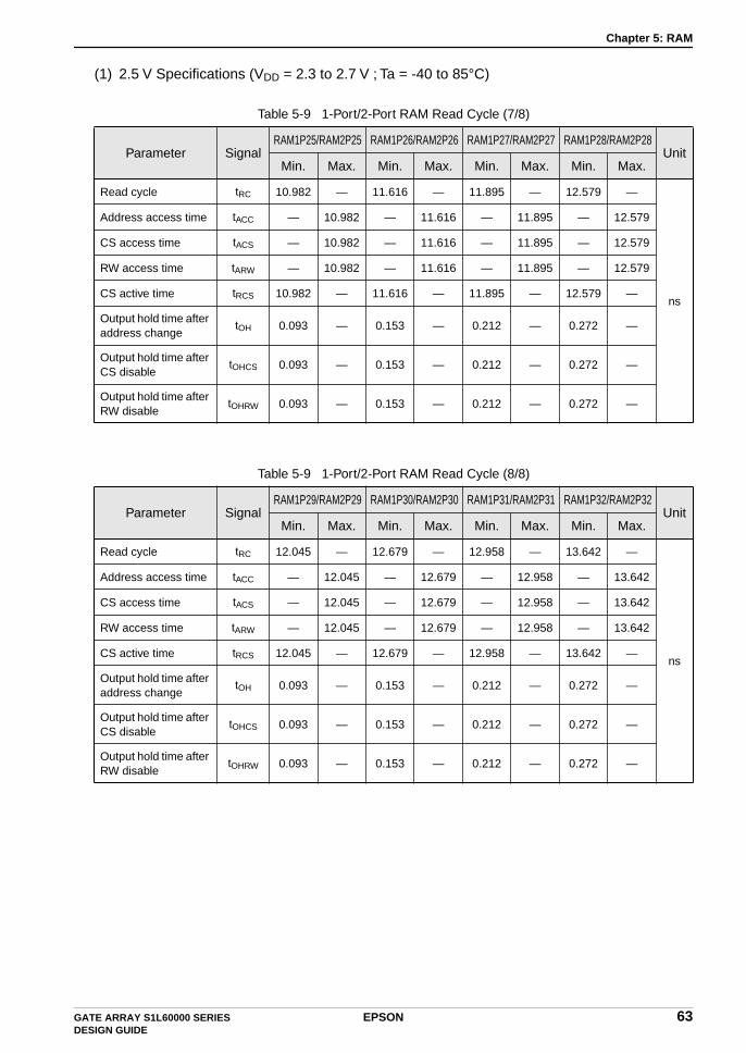
Chapter 5: RAM
(1) 2.5 V Specifications (VDD = 2.3 to 2.7 V ; Ta = -40 to 85°C)
Table 5-9 1-Port/2-Port RAM Read Cycle (7/8)
Parameter SignalRAM1P25/RAM2P25 RAM1P26/RAM2P26 RAM1P27/RAM2P27 RAM1P28/RAM2P28
UnitMin. Max. Min. Max. Min. Max. Min. Max.
Read cycle tRC 10.982 — 11.616 — 11.895 — 12.579 —
ns
Address access time tACC — 10.982 — 11.616 — 11.895 — 12.579
CS access time tACS — 10.982 — 11.616 — 11.895 — 12.579
RW access time tARW — 10.982 — 11.616 — 11.895 — 12.579
CS active time tRCS 10.982 — 11.616 — 11.895 — 12.579 —
Output hold time after address change
tOH 0.093 — 0.153 — 0.212 — 0.272 —
Output hold time after CS disable
tOHCS 0.093 — 0.153 — 0.212 — 0.272 —
Output hold time after RW disable
tOHRW 0.093 — 0.153 — 0.212 — 0.272 —
Table 5-9 1-Port/2-Port RAM Read Cycle (8/8)
Parameter SignalRAM1P29/RAM2P29 RAM1P30/RAM2P30 RAM1P31/RAM2P31 RAM1P32/RAM2P32
UnitMin. Max. Min. Max. Min. Max. Min. Max.
Read cycle tRC 12.045 — 12.679 — 12.958 — 13.642 —
ns
Address access time tACC — 12.045 — 12.679 — 12.958 — 13.642
CS access time tACS — 12.045 — 12.679 — 12.958 — 13.642
RW access time tARW — 12.045 — 12.679 — 12.958 — 13.642
CS active time tRCS 12.045 — 12.679 — 12.958 — 13.642 —
Output hold time after address change
tOH 0.093 — 0.153 — 0.212 — 0.272 —
Output hold time after CS disable
tOHCS 0.093 — 0.153 — 0.212 — 0.272 —
Output hold time after RW disable
tOHRW 0.093 — 0.153 — 0.212 — 0.272 —
GATE ARRAY S1L60000 SERIES EPSON 63DESIGN GUIDE

Chapter 5: RAM
(1) 2.5 V Specifications (VDD = 2.3 to 2.7 V ; Ta = -40 to 85°C)
Table 5-10 1-Port/2-Port RAM Write Cycle (1/8)
Parameter SignalRAM1P1/RAM2P1 RAM1P2/RAM2P2 RAM1P3/RAM2P3 RAM1P4/RAM2P4
UnitMin. Max. Min. Max. Min. Max. Min. Max.
Write cycle tWC 2.776 — 3.624 — 4.520 — 5.396 —
ns
Write pulse width tWP 1.347 — 2.223 — 3.101 — 3.977 —
CS active time tWCS 1.347 — 2.223 — 3.101 — 3.977 —
Address setup time tAS 0.481 — 0.481 — 0.481 — 0.481 —
Address hold time tAH 0.938 — 0.938 — 0.938 — 0.938 —
Data setup time tDS 0.000 — 0.000 — 0.000 — 0.000 —
Data hold time tDH 1.671 — 2.374 — 3.078 — 3.781 —
Table 5-10 1-Port/2-Port RAM Write Cycle (2/8)
Parameter SignalRAM1P5/RAM2P5 RAM1P6/RAM2P6 RAM1P7/RAM2P7 RAM1P8/RAM2P8
UnitMin. Max. Min. Max. Min. Max. Min. Max.
Write cycle tWC 2.924 — 3.799 — 4.677 — 5.553 —
ns
Write pulse width tWP 1.425 — 2.300 — 3.178 — 4.054 —
CS active time tWCS 1.425 — 2.300 — 3.178 — 4.054 —
Address setup time tAS 0.561 — 0.561 — 0.561 — 0.561 —
Address hold time tAH 0.938 — 0.938 — 0.938 — 0.938 —
Data setup time tDS 0.000 — 0.000 — 0.000 — 0.000 —
Data hold time tDH 1.731 — 2.434 — 3.138 — 3.841 —
64 EPSON GATE ARRAY S1L60000 SERIES DESIGN GUIDE

Chapter 5: RAM
(1) 2.5 V Specifications (VDD = 2.3 to 2.7 V ; Ta = -40 to 85°C)
Table 5-10 1-Port/2-Port RAM Write Cycle (3/8)
Parameter SignalRAM1P9/RAM2P9 RAM1P10/RAM2P10 RAM1P11/RAM2P11 RAM1P12/RAM2P12
UnitMin. Max. Min. Max. Min. Max. Min. Max.
Write cycle tWC 3.092 — 3.968 — 4.846 — 5.722 —
ns
Write pulse width tWP 1.513 — 2.389 — 3.267 — 4.143 —
CS active time tWCS 1.513 — 2.389 — 3.267 — 4.143 —
Address setup time tAS 0.641 — 0.641 — 0.641 — 0.641 —
Address hold time tAH 0.938 — 0.938 — 0.938 — 0.938 —
Data setup time tDS 0.000 — 0.000 — 0.000 — 0.000 —
Data hold time tDH 1.791 — 2.495 — 3.198 — 3.901 —
Table 5-10 1-Port/2-Port RAM Write Cycle (4/8)
Parameter SignalRAM1P13/RAM2P13 RAM1P14/RAM2P14 RAM1P15/RAM2P15 RAM1P16/RAM2P16
UnitMin. Max. Min. Max. Min. Max. Min. Max.
Write cycle tWC 3.273 — 4.148 — 5.026 — 5.902 —
ns
Write pulse width tWP 1.614 — 2.489 — 3.367 — 4.243 —
CS active time tWCS 1.614 — 2.489 — 3.367 — 4.243 —
Address setup time tAS 0.721 — 0.721 — 0.721 — 0.721 —
Address hold time tAH 0.938 — 0.938 — 0.938 — 0.938 —
Data setup time tDS 0.000 — 0.000 — 0.000 — 0.000 —
Data hold time tDH 1.851 — 2.555 — 3.258 — 3.961 —
GATE ARRAY S1L60000 SERIES EPSON 65DESIGN GUIDE

Chapter 5: RAM
(1) 2.5 V Specifications (VDD = 2.3 to 2.7 V ; Ta = -40 to 85°C)
Table 5-10 1-Port/2-Port RAM Write Cycle (5/8)
Parameter SignalRAM1P17/RAM2P17 RAM1P18/RAM2P18 RAM1P19/RAM2P19 RAM1P20/RAM2P20
UnitMin. Max. Min. Max. Min. Max. Min. Max.
Write cycle tWC 3.397 — 4.272 — 5.150 — 6.026 —
ns
Write pulse width tWP 1.679 — 2.554 — 3.432 — 4.308 —
CS active time tWCS 1.679 — 2.554 — 3.432 — 4.308 —
Address setup time tAS 0.780 — 0.780 — 0.780 — 0.780 —
Address hold time tAH 0.938 — 0.938 — 0.938 — 0.938 —
Data setup time tDS 0.000 — 0.000 — 0.000 — 0.000 —
Data hold time tDH 1.895 — 2.593 — 3.296 — 4.000 —
Table 5-10 1-Port/2-Port RAM Write Cycle (6/8)
Parameter SignalRAM1P21/RAM2P21 RAM1P22/RAM2P22 RAM1P23/RAM2P23 RAM1P24/RAM2P24
UnitMin. Max. Min. Max. Min. Max. Min. Max.
Write cycle tWC 3.558 — 4.443 — 5.311 — 6.188 —
ns
Write pulse width tWP 1.764 — 2.639 — 3.517 — 4.394 —
CS active time tWCS 1.764 — 2.639 — 3.517 — 4.394 —
Address setup time tAS 0.856 — 0.856 — 0.856 — 0.856 —
Address hold time tAH 0.938 — 0.938 — 0.938 — 0.938 —
Data setup time tDS 0.000 — 0.000 — 0.000 — 0.000 —
Data hold time tDH 1.952 — 2.650 — 3.353 — 4.057 —
66 EPSON GATE ARRAY S1L60000 SERIES DESIGN GUIDE

Chapter 5: RAM
(1) 2.5 V Specifications (VDD = 2.3 to 2.7 V ; Ta = -40 to 85°C)
Table 5-10 1-Port/2-Port RAM Write Cycle (7/8)
Parameter SignalRAM1P25/RAM2P25 RAM1P26/RAM2P26 RAM1P27/RAM2P27 RAM1P28/RAM2P28
UnitMin. Max. Min. Max. Min. Max. Min. Max.
Write cycle tWC 3.720 — 4.595 — 5.473 — 6.349 —
ns
Write pulse width tWP 1.850 — 2.725 — 3.603 — 4.479 —
CS active time tWCS 1.850 — 2.725 — 3.603 — 4.479 —
Address setup time tAS 0.932 — 0.932 — 0.932 — 0.932 —
Address hold time tAH 0.938 — 0.938 — 0.938 — 0.938 —
Data setup time tDS 0.000 — 0.000 — 0.000 — 0.000 —
Data hold time tDH 2.009 — 2.707 — 3.410 — 4.113 —
Table 5-10 1-Port/2-Port RAM Write Cycle (8/8)
Parameter SignalRAM1P29/RAM2P29 RAM1P30/RAM2P30 RAM1P31/RAM2P31 RAM1P32/RAM2P32
UnitMin. Max. Min. Max. Min. Max. Min. Max.
Write cycle tWC 3.880 — 4.755 — 5.633 — 6.509 —
ns
Write pulse width tWP 1.935 — 2.810 — 3.688 — 4.564 —
CS active time tWCS 1.935 — 2.810 — 3.688 — 4.564 —
Address setup time tAS 1.007 — 1.007 — 1.007 — 1.007 —
Address hold time tAH 0.938 — 0.938 — 0.938 — 0.938 —
Data setup time tDS 0.000 — 0.000 — 0.000 — 0.000 —
Data hold time tDH 2.066 — 2.764 — 3.467 — 4.170 —
GATE ARRAY S1L60000 SERIES EPSON 67DESIGN GUIDE

Chapter 5: RAM
(2) 2.5 V Specifications (VDD = 2.3 to 2.7 V ; Ta = 0 to 70°C)
Table 5-11 1-Port/2-Port RAM Read Cycle (1/8)
Parameter SignalRAM1P1/RAM2P1 RAM1P2/RAM2P2 RAM1P3/RAM2P3 RAM1P4/RAM2P4
UnitMin. Max. Min. Max. Min. Max. Min. Max.
Read cycle tRC 4.356 — 4.956 — 5.220 — 5.868 —
ns
Address access time tACC — 4.356 — 4.956 — 5.220 — 5.868
CS access time tACS — 4.356 — 4.956 — 5.220 — 5.868
RW access time tARW — 4.356 — 4.956 — 5.220 — 5.868
CS active time tRCS 4.356 — 4.956 — 5.220 — 5.868 —
Output hold time after address change
tOH 0.099 — 0.163 — 0.226 — 0.289 —
Output hold time after CS disable
tOHCS 0.099 — 0.163 — 0.226 — 0.289 —
Output hold time after RW disable
tOHRW 0.099 — 0.163 — 0.226 — 0.289 —
Table 5-11 1-Port/2-Port RAM Read Cycle (2/8)
Parameter SignalRAM1P5/RAM2P5 RAM1P6/RAM2P6 RAM1P7/RAM2P7 RAM1P8/RAM2P8
UnitMin. Max. Min. Max. Min. Max. Min. Max.
Read cycle tRC 5.362 — 5.961 — 6.226 — 6.873 —
ns
Address access time tACC — 5.362 — 5.961 — 6.226 — 6.873
CS access time tACS — 5.362 — 5.961 — 6.226 — 6.873
RW access time tARW — 5.362 — 5.961 — 6.226 — 6.873
CS active time tRCS 5.362 — 5.961 — 6.226 — 6.873 —
Output hold time after address change
tOH 0.099 — 0.163 — 0.226 — 0.289 —
Output hold time after CS disable
tOHCS 0.099 — 0.163 — 0.226 — 0.289 —
Output hold time after RW disable
tOHRW 0.099 — 0.163 — 0.226 — 0.289 —
68 EPSON GATE ARRAY S1L60000 SERIES DESIGN GUIDE

Chapter 5: RAM
(2) 2.5 V Specifications (VDD = 2.3 to 2.7 V ; Ta = 0 to 70°C)
Table 5-11 1-Port/2-Port RAM Read Cycle (3/8)
Parameter SignalRAM1P9/RAM2P9 RAM1P10/RAM2P10 RAM1P11/RAM2P11 RAM1P12/RAM2P12
UnitMin. Max. Min. Max. Min. Max. Min. Max.
Read cycle tRC 6.367 — 6.967 — 7.231 — 7.878 —
ns
Address access time tACC — 6.367 — 6.967 — 7.231 — 7.878
CS access time tACS — 6.367 — 6.967 — 7.231 — 7.878
RW access time tARW — 6.367 — 6.967 — 7.231 — 7.878
CS active time tRCS 6.367 — 6.967 — 7.231 — 7.878 —
Output hold time after address change
tOH 0.099 — 0.163 — 0.226 — 0.289 —
Output hold time after CS disable
tOHCS 0.099 — 0.163 — 0.226 — 0.289 —
Output hold time after RW disable
tOHRW 0.099 — 0.163 — 0.226 — 0.289 —
Table 5-11 1-Port/2-Port RAM Read Cycle (4/8)
Parameter SignalRAM1P13/RAM2P13 RAM1P14/RAM2P14 RAM1P15/RAM2P15 RAM1P16/RAM2P16
UnitMin. Max. Min. Max. Min. Max. Min. Max.
Read cycle tRC 7.372 — 7.972 — 8.236 — 8.884 —
ns
Address access time tACC — 7.372 — 7.972 — 8.236 — 8.884
CS access time tACS — 7.372 — 7.972 — 8.236 — 8.884
RW access time tARW — 7.372 — 7.972 — 8.236 — 8.884
CS active time tRCS 7.372 — 7.972 — 8.236 — 8.884 —
Output hold time after address change
tOH 0.099 — 0.163 — 0.226 — 0.289 —
Output hold time after CS disable
tOHCS 0.099 — 0.163 — 0.226 — 0.289 —
Output hold time after RW disable
tOHRW 0.099 — 0.163 — 0.226 — 0.289 —
GATE ARRAY S1L60000 SERIES EPSON 69DESIGN GUIDE

Chapter 5: RAM
(2) 2.5 V Specifications (VDD = 2.3 to 2.7 V ; Ta = 0 to 70°C)
Table 5-11 1-Port/2-Port RAM Read Cycle (5/8)
Parameter SignalRAM1P17/RAM2P17 RAM1P18/RAM2P18 RAM1P19/RAM2P19 RAM1P20/RAM2P20
UnitMin. Max. Min. Max. Min. Max. Min. Max.
Read cycle tRC 8.378 — 8.977 — 9.242 — 9.889 —
ns
Address access time tACC — 8.378 — 8.977 — 9.242 — 9.889
CS access time tACS — 8.378 — 8.977 — 9.242 — 9.889
RW access time tARW — 8.378 — 8.977 — 9.242 — 9.889
CS active time tRCS 8.378 — 8.977 — 9.242 — 9.889 —
Output hold time after address change
tOH 0.099 — 0.163 — 0.226 — 0.289 —
Output hold time after CS disable
tOHCS 0.099 — 0.163 — 0.226 — 0.289 —
Output hold time after RW disable
tOHRW 0.099 — 0.163 — 0.226 — 0.289 —
Table 5-11 1-Port/2-Port RAM Read Cycle (6/8)
Parameter SignalRAM1P21/RAM2P21 RAM1P22/RAM2P22 RAM1P23/RAM2P23 RAM1P24/RAM2P24
UnitMin. Max. Min. Max. Min. Max. Min. Max.
Read cycle tRC 9.383 — 9.983 — 10.247 — 10.894 —
ns
Address access time tACC — 9.383 — 9.983 — 10.247 — 10.894
CS access time tACS — 9.383 — 9.983 — 10.247 — 10.894
RW access time tARW — 9.383 — 9.983 — 10.247 — 10.894
CS active time tRCS 9.383 — 9.983 — 10.247 — 10.894 —
Output hold time after address change
tOH 0.099 — 0.163 — 0.226 — 0.289 —
Output hold time after CS disable
tOHCS 0.099 — 0.163 — 0.226 — 0.289 —
Output hold time after RW disable
tOHRW 0.099 — 0.163 — 0.226 — 0.289 —
70 EPSON GATE ARRAY S1L60000 SERIES DESIGN GUIDE

Chapter 5: RAM
(2) 2.5 V Specifications (VDD = 2.3 to 2.7 V ; Ta = 0 to 70°C)
Table 5-11 1-Port/2-Port RAM Read Cycle (7/8)
Parameter SignalRAM1P25/RAM2P25 RAM1P26/RAM2P26 RAM1P27/RAM2P27 RAM1P28/RAM2P28
UnitMin. Max. Min. Max. Min. Max. Min. Max.
Read cycle tRC 10.388 — 10.988 — 11.252 — 11.900 —
ns
Address access time tACC — 10.388 — 10.988 — 11.252 — 11.900
CS access time tACS — 10.388 — 10.988 — 11.252 — 11.900
RW access time tARW — 10.388 — 10.988 — 11.252 — 11.900
CS active time tRCS 10.388 — 10.988 — 11.252 — 11.900 —
Output hold time after address change
tOH 0.099 — 0.163 — 0.226 — 0.289 —
Output hold time after CS disable
tOHCS 0.099 — 0.163 — 0.226 — 0.289 —
Output hold time after RW disable
tOHRW 0.099 — 0.163 — 0.226 — 0.289 —
Table 5-11 1-Port/2-Port RAM Read Cycle (8/8)
Parameter SignalRAM1P29/RAM2P29 RAM1P30/RAM2P30 RAM1P31/RAM2P31 RAM1P32/RAM2P32
UnitMin. Max. Min. Max. Min. Max. Min. Max.
Read cycle tRC 11.394 — 11.993 — 12.257 — 12.905 —
ns
Address access time tACC — 11.394 — 11.993 — 12.257 — 12.905
CS access time tACS — 11.394 — 11.993 — 12.257 — 12.905
RW access time tARW — 11.394 — 11.993 — 12.257 — 12.905
CS active time tRCS 11.394 — 11.993 — 12.257 — 12.905 —
Output hold time after address change
tOH 0.099 — 0.163 — 0.226 — 0.289 —
Output hold time after CS disable
tOHCS 0.099 — 0.163 — 0.226 — 0.289 —
Output hold time after RW disable
tOHRW 0.099 — 0.163 — 0.226 — 0.289 —
GATE ARRAY S1L60000 SERIES EPSON 71DESIGN GUIDE

Chapter 5: RAM
(2) 2.5 V Specifications (VDD = 2.3 to 2.7 V ; Ta = 0 to 70°C)
Table 5-12 1-Port/2-Port RAM Write Cycle (1/8)
Parameter SignalRAM1P1/RAM2P1 RAM1P2/RAM2P2 RAM1P3/RAM2P3 RAM1P4/RAM2P4
UnitMin. Max. Min. Max. Min. Max. Min. Max.
Write cycle tWC 2.617 — 3.444 — 4.275 — 5.104 —
ns
Write pulse width tWP 1.275 — 2.102 — 2.933 — 3.762 —
CS active time tWCS 1.275 — 2.102 — 2.933 — 3.762 —
Address setup time tAS 0.455 — 0.455 — 0.455 — 0.455 —
Address hold time tAH 0.887 — 0.887 — 0.887 — 0.887 —
Data setup time tDS 0.000 — 0.000 — 0.000 — 0.000 —
Data hold time tDH 1.581 — 2.246 — 2.911 — 3.577 —
Table 5-12 1-Port/2-Port RAM Write Cycle (2/8)
Parameter SignalRAM1P5/RAM2P5 RAM1P6/RAM2P6 RAM1P7/RAM2P7 RAM1P8/RAM2P8
UnitMin. Max. Min. Max. Min. Max. Min. Max.
Write cycle tWC 2.766 — 3.594 — 4.424 — 5.253 —
ns
Write pulse width tWP 1.348 — 2.176 — 3.006 — 3.835 —
CS active time tWCS 1.348 — 2.176 — 3.006 — 3.835 —
Address setup time tAS 0.531 — 0.531 — 0.531 — 0.531 —
Address hold time tAH 0.887 — 0.887 — 0.887 — 0.887 —
Data setup time tDS 0.000 — 0.000 — 0.000 — 0.000 —
Data hold time tDH 1.638 — 2.303 — 2.968 — 3.633 —
72 EPSON GATE ARRAY S1L60000 SERIES DESIGN GUIDE

Chapter 5: RAM
(2) 2.5 V Specifications (VDD = 2.3 to 2.7 V ; Ta = 0 to 70°C)
Table 5-12 1-Port/2-Port RAM Write Cycle (3/8)
Parameter SignalRAM1P9/RAM2P9 RAM1P10/RAM2P10 RAM1P11/RAM2P11 RAM1P12/RAM2P12
UnitMin. Max. Min. Max. Min. Max. Min. Max.
Write cycle tWC 2.926 — 3.754 — 4.584 — 5.413 —
ns
Write pulse width tWP 1.432 — 2.260 — 3.090 — 3.919 —
CS active time tWCS 1.432 — 2.260 — 3.090 — 3.919 —
Address setup time tAS 0.607 — 0.607 — 0.607 — 0.607 —
Address hold time tAH 0.887 — 0.887 — 0.887 — 0.887 —
Data setup time tDS 0.000 — 0.000 — 0.000 — 0.000 —
Data hold time tDH 1.694 — 2.360 — 3.025 — 3.690 —
Table 5-12 1-Port/2-Port RAM Write Cycle (4/8)
Parameter SignalRAM1P13/RAM2P13 RAM1P14/RAM2P14 RAM1P15/RAM2P15 RAM1P16/RAM2P16
UnitMin. Max. Min. Max. Min. Max. Min. Max.
Write cycle tWC 3.096 — 3.923 — 4.754 — 5.583 —
ns
Write pulse width tWP 1.527 — 2.354 — 3.185 — 4.014 —
CS active time tWCS 1.527 — 2.354 — 3.185 — 4.014 —
Address setup time tAS 0.682 — 0.682 — 0.682 — 0.682 —
Address hold time tAH 0.887 — 0.887 — 0.887 — 0.887 —
Data setup time tDS 0.000 — 0.000 — 0.000 — 0.000 —
Data hold time tDH 1.751 — 2.416 — 3.082 — 3.747 —
GATE ARRAY S1L60000 SERIES EPSON 73DESIGN GUIDE

Chapter 5: RAM
(2) 2.5 V Specifications (VDD = 2.3 to 2.7 V ; Ta = 0 to 70°C)
Table 5-12 1-Port/2-Port RAM Write Cycle (5/8)
Parameter SignalRAM1P17/RAM2P17 RAM1P18/RAM2P18 RAM1P19/RAM2P19 RAM1P20/RAM2P20
UnitMin. Max. Min. Max. Min. Max. Min. Max.
Write cycle tWC 3.213 — 4.041 — 4.872 — 5.701 —
ns
Write pulse width tWP 1.588 — 2.416 — 3.247 — 4.076 —
CS active time tWCS 1.588 — 2.416 — 3.247 — 4.076 —
Address setup time tAS 0.738 — 0.738 — 0.738 — 0.738 —
Address hold time tAH 0.887 — 0.887 — 0.887 — 0.887 —
Data setup time tDS 0.000 — 0.000 — 0.000 — 0.000 —
Data hold time tDH 1.793 — 2.453 — 3.118 — 3.784 —
Table 5-12 1-Port/2-Port RAM Write Cycle (6/8)
Parameter SignalRAM1P21/RAM2P21 RAM1P22/RAM2P22 RAM1P23/RAM2P23 RAM1P24/RAM2P24
UnitMin. Max. Min. Max. Min. Max. Min. Max.
Write cycle tWC 3.366 — 4.194 — 5.024 — 5.853 —
ns
Write pulse width tWP 1.669 — 2.497 — 3.327 — 4.156 —
CS active time tWCS 1.669 — 2.497 — 3.327 — 4.156 —
Address setup time tAS 0.810 — 0.810 — 0.810 — 0.810 —
Address hold time tAH 0.887 — 0.887 — 0.887 — 0.887 —
Data setup time tDS 0.000 — 0.000 — 0.000 — 0.000 —
Data hold time tDH 1.847 — 2.507 — 3.172 — 3.837 —
74 EPSON GATE ARRAY S1L60000 SERIES DESIGN GUIDE
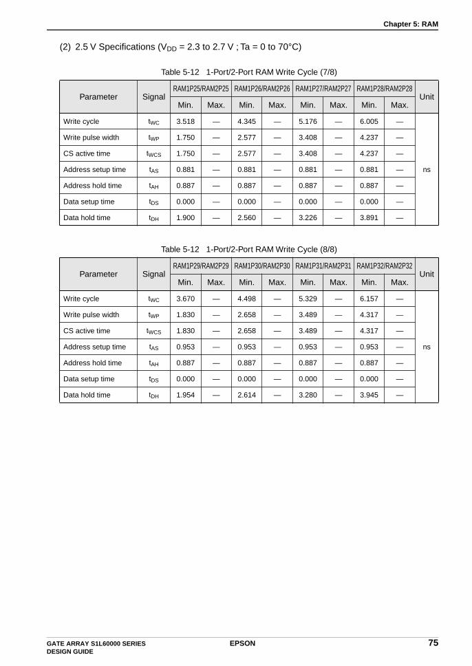
Chapter 5: RAM
(2) 2.5 V Specifications (VDD = 2.3 to 2.7 V ; Ta = 0 to 70°C)
Table 5-12 1-Port/2-Port RAM Write Cycle (7/8)
Parameter SignalRAM1P25/RAM2P25 RAM1P26/RAM2P26 RAM1P27/RAM2P27 RAM1P28/RAM2P28
UnitMin. Max. Min. Max. Min. Max. Min. Max.
Write cycle tWC 3.518 — 4.345 — 5.176 — 6.005 —
ns
Write pulse width tWP 1.750 — 2.577 — 3.408 — 4.237 —
CS active time tWCS 1.750 — 2.577 — 3.408 — 4.237 —
Address setup time tAS 0.881 — 0.881 — 0.881 — 0.881 —
Address hold time tAH 0.887 — 0.887 — 0.887 — 0.887 —
Data setup time tDS 0.000 — 0.000 — 0.000 — 0.000 —
Data hold time tDH 1.900 — 2.560 — 3.226 — 3.891 —
Table 5-12 1-Port/2-Port RAM Write Cycle (8/8)
Parameter SignalRAM1P29/RAM2P29 RAM1P30/RAM2P30 RAM1P31/RAM2P31 RAM1P32/RAM2P32
UnitMin. Max. Min. Max. Min. Max. Min. Max.
Write cycle tWC 3.670 — 4.498 — 5.329 — 6.157 —
ns
Write pulse width tWP 1.830 — 2.658 — 3.489 — 4.317 —
CS active time tWCS 1.830 — 2.658 — 3.489 — 4.317 —
Address setup time tAS 0.953 — 0.953 — 0.953 — 0.953 —
Address hold time tAH 0.887 — 0.887 — 0.887 — 0.887 —
Data setup time tDS 0.000 — 0.000 — 0.000 — 0.000 —
Data hold time tDH 1.954 — 2.614 — 3.280 — 3.945 —
GATE ARRAY S1L60000 SERIES EPSON 75DESIGN GUIDE

Chapter 5: RAM
(3) 2.0 V Specifications (VDD = 1.8 to 2.2 V; Ta = -40 to 85°C)
Table 5-13 1-Port/2-Port RAM Read Cycle (1/8)
Parameter SignalRAM1P1/RAM2P1 RAM1P2/RAM2P2 RAM1P3/RAM2P3 RAM1P4/RAM2P4
UnitMin. Max. Min. Max. Min. Max. Min. Max.
Read cycle tRC 6.804 — 7.736 — 8.134 — 9.109 —
ns
Address access time tACC — 6.804 — 7.736 — 8.134 — 9.109
CS access time tACS — 6.804 — 7.736 — 8.134 — 9.109
RW access time tARW — 6.804 — 7.736 — 8.134 — 9.109
CS active time tRCS 6.804 — 7.736 — 8.134 — 9.109 —
Output hold time after address change
tOH 0.182 — 0.257 — 0.332 — 0.407 —
Output hold time after CS disable
tOHCS 0.182 — 0.257 — 0.332 — 0.407 —
Output hold time after RW disable
tOHRW 0.182 — 0.257 — 0.332 — 0.407 —
Table 5-13 1-Port/2-Port RAM Read Cycle (2/8)
Parameter SignalRAM1P5/RAM2P5 RAM1P6/RAM2P6 RAM1P7/RAM2P7 RAM1P8/RAM2P8
UnitMin. Max. Min. Max. Min. Max. Min. Max.
Read cycle tRC 8.450 — 9.382 — 9.781 — 10.755 —
ns
Address access time tACC — 8.450 — 9.382 — 9.781 — 10.755
CS access time tACS — 8.450 — 9.382 — 9.781 — 10.755
RW access time tARW — 8.450 — 9.382 — 9.781 — 10.755
CS active time tRCS 8.450 — 9.382 — 9.781 — 10.755 —
Output hold time after address change
tOH 0.182 — 0.257 — 0.332 — 0.407 —
Output hold time after CS disable
tOHCS 0.182 — 0.257 — 0.332 — 0.407 —
Output hold time after RW disable
tOHRW 0.182 — 0.257 — 0.332 — 0.407 —
76 EPSON GATE ARRAY S1L60000 SERIES DESIGN GUIDE

Chapter 5: RAM
(3) 2.0 V Specifications (VDD = 1.8 to 2.2 V; Ta = -40 to 85°C)
Table 5-13 1-Port/2-Port RAM Read Cycle (3/8)
Parameter SignalRAM1P9/RAM2P9 RAM1P10/RAM2P10 RAM1P11/RAM2P11 RAM1P12/RAM2P12
UnitMin. Max. Min. Max. Min. Max. Min. Max.
Read cycle tRC 10.096 — 11.028 — 11.427 — 12.402 —
ns
Address access time tACC — 10.096 — 11.028 — 11.427 — 12.402
CS access time tACS — 10.096 — 11.028 — 11.427 — 12.402
RW access time tARW — 10.096 — 11.028 — 11.427 — 12.402
CS active time tRCS 10.096 — 11.028 — 11.427 — 12.402 —
Output hold time after address change
tOH 0.182 — 0.257 — 0.332 — 0.407 —
Output hold time after CS disable
tOHCS 0.182 — 0.257 — 0.332 — 0.407 —
Output hold time after RW disable
tOHRW 0.182 — 0.257 — 0.332 — 0.407 —
Table 5-13 1-Port/2-Port RAM Read Cycle (4/8)
Parameter SignalRAM1P13/RAM2P13 RAM1P14/RAM2P14 RAM1P15/RAM2P15 RAM1P16/RAM2P16
UnitMin. Max. Min. Max. Min. Max. Min. Max.
Read cycle tRC 11.743 — 12.675 — 13.074 — 14.048 —
ns
Address access time tACC — 11.743 — 12.675 — 13.074 — 14.048
CS access time tACS — 11.743 — 12.675 — 13.074 — 14.048
RW access time tARW — 11.743 — 12.675 — 13.074 — 14.048
CS active time tRCS 11.743 — 12.675 — 13.074 — 14.048 —
Output hold time after address change
tOH 0.182 — 0.257 — 0.332 — 0.407 —
Output hold time after CS disable
tOHCS 0.182 — 0.257 — 0.332 — 0.407 —
Output hold time after RW disable
tOHRW 0.182 — 0.257 — 0.332 — 0.407 —
GATE ARRAY S1L60000 SERIES EPSON 77DESIGN GUIDE

Chapter 5: RAM
(3) 2.0 V Specifications (VDD = 1.8 to 2.2 V; Ta = -40 to 85°C)
Table 5-13 1-Port/2-Port RAM Read Cycle (5/8)
Parameter SignalRAM1P17/RAM2P17 RAM1P18/RAM2P18 RAM1P19/RAM2P19 RAM1P20/RAM2P20
UnitMin. Max. Min. Max. Min. Max. Min. Max.
Read cycle tRC 13.389 — 14.321 — 14.720 — 15.694 —
ns
Address access time tACC — 13.389 — 14.321 — 14.720 — 15.694
CS access time tACS — 13.389 — 14.321 — 14.720 — 15.694
RW access time tARW — 13.389 — 14.321 — 14.720 — 15.694
CS active time tRCS 13.389 — 14.321 — 14.720 — 15.694 —
Output hold time after address change
tOH 0.182 — 0.257 — 0.332 — 0.407 —
Output hold time after CS disable
tOHCS 0.182 — 0.257 — 0.332 — 0.407 —
Output hold time after RW disable
tOHRW 0.182 — 0.257 — 0.332 — 0.407 —
Table 5-13 1-Port/2-Port RAM Read Cycle (6/8)
Parameter SignalRAM1P21/RAM2P21 RAM1P22/RAM2P22 RAM1P23/RAM2P23 RAM1P24/RAM2P24
UnitMin. Max. Min. Max. Min. Max. Min. Max.
Read cycle tRC 15.036 — 15.967 — 16.366 — 17.341 —
ns
Address access time tACC — 15.036 — 15.967 — 16.366 — 17.341
CS access time tACS — 15.036 — 15.967 — 16.366 — 17.341
RW access time tARW — 15.036 — 15.967 — 16.366 — 17.341
CS active time tRCS 15.036 — 15.967 — 16.366 — 17.341 —
Output hold time after address change
tOH 0.182 — 0.257 — 0.332 — 0.407 —
Output hold time after CS disable
tOHCS 0.182 — 0.257 — 0.332 — 0.407 —
Output hold time after RW disable
tOHRW 0.182 — 0.257 — 0.332 — 0.407 —
78 EPSON GATE ARRAY S1L60000 SERIES DESIGN GUIDE

Chapter 5: RAM
(3) 2.0 V Specifications (VDD = 1.8 to 2.2 V; Ta = -40 to 85°C)
Table 5-13 1-Port/2-Port RAM Read Cycle (7/8)
Parameter SignalRAM1P25/RAM2P25 RAM1P26/RAM2P26 RAM1P27/RAM2P27 RAM1P28/RAM2P28
UnitMin. Max. Min. Max. Min. Max. Min. Max.
Read cycle tRC 16.682 — 17.614 — 18.013 — 18.987 —
ns
Address access time tACC — 16.682 — 17.614 — 18.013 — 18.987
CS access time tACS — 16.682 — 17.614 — 18.013 — 18.987
RW access time tARW — 16.682 — 17.614 — 18.013 — 18.987
CS active time tRCS 16.682 — 17.614 — 18.013 — 18.987 —
Output hold time after address change
tOH 0.182 — 0.257 — 0.332 — 0.407 —
Output hold time after CS disable
tOHCS 0.182 — 0.257 — 0.332 — 0.407 —
Output hold time after RW disable
tOHRW 0.182 — 0.257 — 0.332 — 0.407 —
Table 5-13 1-Port/2-Port RAM Read Cycle (8/8)
Parameter SignalRAM1P29/RAM2P29 RAM1P30/RAM2P30 RAM1P31/RAM2P31 RAM1P32/RAM2P32
UnitMin. Max. Min. Max. Min. Max. Min. Max.
Read cycle tRC 18.328 — 19.260 — 19.659 — 20.633 —
ns
Address access time tACC — 18.328 — 19.260 — 19.659 — 20.633
CS access time tACS — 18.328 — 19.260 — 19.659 — 20.633
RW access time tARW — 18.328 — 19.260 — 19.659 — 20.633
CS active time tRCS 18.328 — 19.260 — 19.659 — 20.633 —
Output hold time after address change
tOH 0.182 — 0.257 — 0.332 — 0.407 —
Output hold time after CS disable
tOHCS 0.182 — 0.257 — 0.332 — 0.407 —
Output hold time after RW disable
tOHRW 0.182 — 0.257 — 0.332 — 0.407 —
GATE ARRAY S1L60000 SERIES EPSON 79DESIGN GUIDE

Chapter 5: RAM
(3) 2.0 V Specifications (VDD = 1.8 to 2.2 V; Ta = -40 to 85°C)
Table 5-14 1-Port/2-Port RAM Write Cycle (1/8)
Parameter SignalRAM1P1/RAM2P1 RAM1P2/RAM2P2 RAM1P3/RAM2P3 RAM1P4/RAM2P4
UnitMin. Max. Min. Max. Min. Max. Min. Max.
Write cycle tWC 4.807 — 6.341 — 7.878 — 9.413 —
ns
Write pulse width tWP 2.720 — 4.254 — 5.791 — 7.326 —
CS active time tWCS 2.720 — 4.254 — 5.791 — 7.326 —
Address setup time tAS 0.696 — 0.696 — 0.696 — 0.696 —
Address hold time tAH 1.391 — 1.391 — 1.391 — 1.391 —
Data setup time tDS 0.000 — 0.000 — 0.000 — 0.000 —
Data hold time tDH 2.652 — 3.712 — 4.773 — 5.834 —
Table 5-14 1-Port/2-Port RAM Write Cycle (2/8)
Parameter SignalRAM1P5/RAM2P5 RAM1P6/RAM2P6 RAM1P7/RAM2P7 RAM1P8/RAM2P8
UnitMin. Max. Min. Max. Min. Max. Min. Max.
Write cycle tWC 5.008 — 6.542 — 8.079 — 9.614 —
ns
Write pulse width tWP 2.822 — 4.356 — 5.893 — 7.428 —
CS active time tWCS 2.822 — 4.356 — 5.893 — 7.428 —
Address setup time tAS 0.795 — 0.795 — 0.795 — 0.795 —
Address hold time tAH 1.391 — 1.391 — 1.391 — 1.391 —
Data setup time tDS 0.000 — 0.000 — 0.000 — 0.000 —
Data hold time tDH 2.744 — 3.804 — 4.866 — 5.926 —
80 EPSON GATE ARRAY S1L60000 SERIES DESIGN GUIDE

Chapter 5: RAM
(3) 2.0 V Specifications (VDD = 1.8 to 2.2 V; Ta = -40 to 85°C)
Table 5-14 1-Port/2-Port RAM Write Cycle (3/8)
Parameter SignalRAM1P9/RAM2P9 RAM1P10/RAM2P10 RAM1P11/RAM2P11 RAM1P12/RAM2P12
UnitMin. Max. Min. Max. Min. Max. Min. Max.
Write cycle tWC 5.238 — 6.772 — 8.309 — 9.844 —
ns
Write pulse width tWP 2.953 — 4.487 — 6.024 — 7.559 —
CS active time tWCS 2.953 — 4.487 — 6.024 — 7.559 —
Address setup time tAS 0.894 — 0.894 — 0.894 — 0.894 —
Address hold time tAH 1.391 — 1.391 — 1.391 — 1.391 —
Data setup time tDS 0.000 — 0.000 — 0.000 — 0.000 —
Data hold time tDH 2.836 — 3.897 — 4.958 — 6.019 —
Table 5-14 1-Port/2-Port RAM Write Cycle (4/8)
Parameter SignalRAM1P13/RAM2P13 RAM1P14/RAM2P14 RAM1P15/RAM2P15 RAM1P16/RAM2P16
UnitMin. Max. Min. Max. Min. Max. Min. Max.
Write cycle tWC 5.497 — 7.031 — 8.568 — 10.103 —
ns
Write pulse width tWP 3.113 — 4.647 — 6.184 — 7.719 —
CS active time tWCS 3.113 — 4.647 — 6.184 — 7.719 —
Address setup time tAS 0.993 — 0.993 — 0.993 — 0.993 —
Address hold time tAH 1.391 — 1.391 — 1.391 — 1.391 —
Data setup time tDS 0.000 — 0.000 — 0.000 — 0.000 —
Data hold time tDH 2.928 — 3.989 — 5.050 — 6.111 —
GATE ARRAY S1L60000 SERIES EPSON 81DESIGN GUIDE
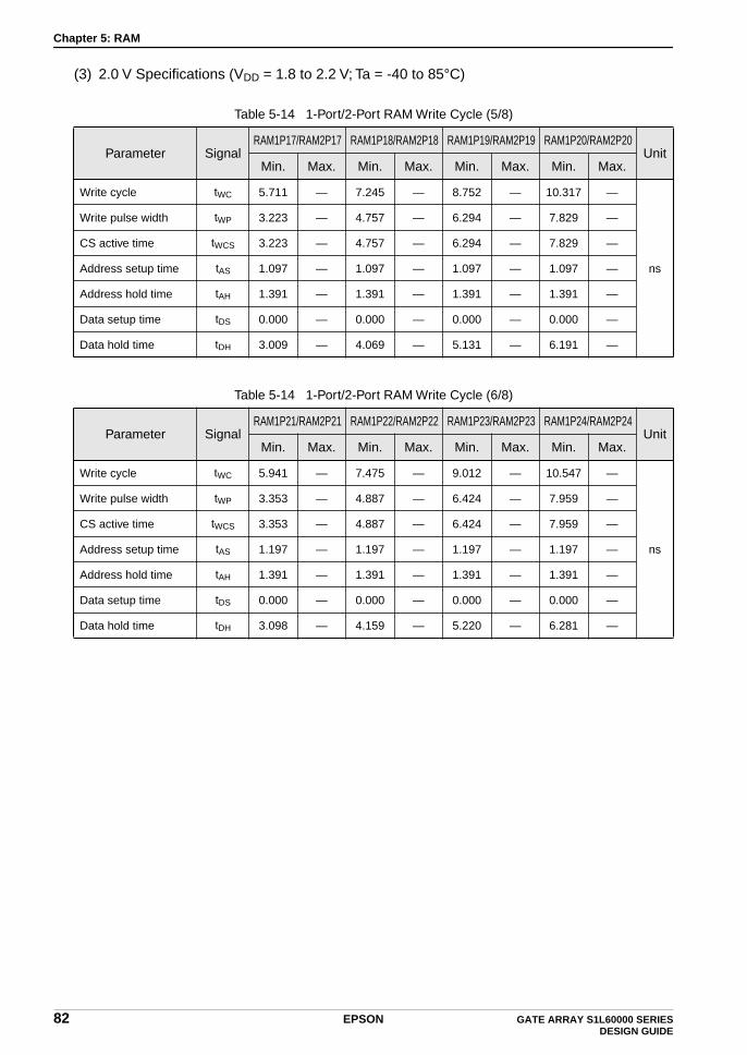
Chapter 5: RAM
(3) 2.0 V Specifications (VDD = 1.8 to 2.2 V; Ta = -40 to 85°C)
Table 5-14 1-Port/2-Port RAM Write Cycle (5/8)
Parameter SignalRAM1P17/RAM2P17 RAM1P18/RAM2P18 RAM1P19/RAM2P19 RAM1P20/RAM2P20
UnitMin. Max. Min. Max. Min. Max. Min. Max.
Write cycle tWC 5.711 — 7.245 — 8.752 — 10.317 —
ns
Write pulse width tWP 3.223 — 4.757 — 6.294 — 7.829 —
CS active time tWCS 3.223 — 4.757 — 6.294 — 7.829 —
Address setup time tAS 1.097 — 1.097 — 1.097 — 1.097 —
Address hold time tAH 1.391 — 1.391 — 1.391 — 1.391 —
Data setup time tDS 0.000 — 0.000 — 0.000 — 0.000 —
Data hold time tDH 3.009 — 4.069 — 5.131 — 6.191 —
Table 5-14 1-Port/2-Port RAM Write Cycle (6/8)
Parameter SignalRAM1P21/RAM2P21 RAM1P22/RAM2P22 RAM1P23/RAM2P23 RAM1P24/RAM2P24
UnitMin. Max. Min. Max. Min. Max. Min. Max.
Write cycle tWC 5.941 — 7.475 — 9.012 — 10.547 —
ns
Write pulse width tWP 3.353 — 4.887 — 6.424 — 7.959 —
CS active time tWCS 3.353 — 4.887 — 6.424 — 7.959 —
Address setup time tAS 1.197 — 1.197 — 1.197 — 1.197 —
Address hold time tAH 1.391 — 1.391 — 1.391 — 1.391 —
Data setup time tDS 0.000 — 0.000 — 0.000 — 0.000 —
Data hold time tDH 3.098 — 4.159 — 5.220 — 6.281 —
82 EPSON GATE ARRAY S1L60000 SERIES DESIGN GUIDE

Chapter 5: RAM
(3) 2.0 V Specifications (VDD = 1.8 to 2.2 V; Ta = -40 to 85°C)
Table 5-14 1-Port/2-Port RAM Write Cycle (7/8)
Parameter SignalRAM1P25/RAM2P25 RAM1P26/RAM2P26 RAM1P27/RAM2P27 RAM1P28/RAM2P28
UnitMin. Max. Min. Max. Min. Max. Min. Max.
Write cycle tWC 6.171 — 7.705 — 9.242 — 10.777 —
ns
Write pulse width tWP 3.483 — 5.017 — 6.554 — 8.089 —
CS active time tWCS 3.483 — 5.017 — 6.554 — 8.089 —
Address setup time tAS 1.297 — 1.297 — 1.297 — 1.297 —
Address hold time tAH 1.391 — 1.391 — 1.391 — 1.391 —
Data setup time tDS 0.000 — 0.000 — 0.000 — 0.000 —
Data hold time tDH 3.188 — 4.249 — 5.310 — 6.371 —
Table 5-14 1-Port/2-Port RAM Write Cycle (8/8)
Parameter SignalRAM1P29/RAM2P29 RAM1P30/RAM2P30 RAM1P31/RAM2P31 RAM1P32/RAM2P32
UnitMin. Max. Min. Max. Min. Max. Min. Max.
Write cycle tWC 6.400 — 7.934 — 9.471 — 11.006 —
ns
Write pulse width tWP 3.613 — 5.147 — 6.684 — 8.219 —
CS active time tWCS 3.613 — 5.147 — 6.684 — 8.219 —
Address setup time tAS 1.396 — 1.396 — 1.396 — 1.396 —
Address hold time tAH 1.391 — 1.391 — 1.391 — 1.391 —
Data setup time tDS 0.000 — 0.000 — 0.000 — 0.000 —
Data hold time tDH 3.278 — 4.339 — 5.400 — 6.461 —
GATE ARRAY S1L60000 SERIES EPSON 83DESIGN GUIDE
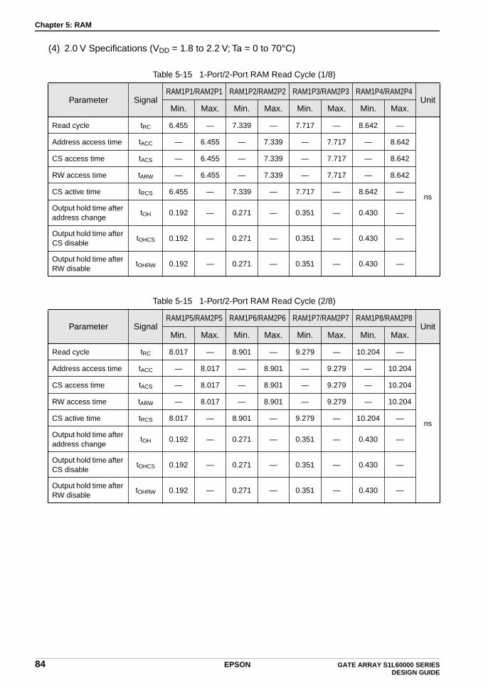
Chapter 5: RAM
(4) 2.0 V Specifications (VDD = 1.8 to 2.2 V; Ta = 0 to 70°C)
Table 5-15 1-Port/2-Port RAM Read Cycle (1/8)
Parameter SignalRAM1P1/RAM2P1 RAM1P2/RAM2P2 RAM1P3/RAM2P3 RAM1P4/RAM2P4
UnitMin. Max. Min. Max. Min. Max. Min. Max.
Read cycle tRC 6.455 — 7.339 — 7.717 — 8.642 —
ns
Address access time tACC — 6.455 — 7.339 — 7.717 — 8.642
CS access time tACS — 6.455 — 7.339 — 7.717 — 8.642
RW access time tARW — 6.455 — 7.339 — 7.717 — 8.642
CS active time tRCS 6.455 — 7.339 — 7.717 — 8.642 —
Output hold time after address change
tOH 0.192 — 0.271 — 0.351 — 0.430 —
Output hold time after CS disable
tOHCS 0.192 — 0.271 — 0.351 — 0.430 —
Output hold time after RW disable
tOHRW 0.192 — 0.271 — 0.351 — 0.430 —
Table 5-15 1-Port/2-Port RAM Read Cycle (2/8)
Parameter SignalRAM1P5/RAM2P5 RAM1P6/RAM2P6 RAM1P7/RAM2P7 RAM1P8/RAM2P8
UnitMin. Max. Min. Max. Min. Max. Min. Max.
Read cycle tRC 8.017 — 8.901 — 9.279 — 10.204 —
ns
Address access time tACC — 8.017 — 8.901 — 9.279 — 10.204
CS access time tACS — 8.017 — 8.901 — 9.279 — 10.204
RW access time tARW — 8.017 — 8.901 — 9.279 — 10.204
CS active time tRCS 8.017 — 8.901 — 9.279 — 10.204 —
Output hold time after address change
tOH 0.192 — 0.271 — 0.351 — 0.430 —
Output hold time after CS disable
tOHCS 0.192 — 0.271 — 0.351 — 0.430 —
Output hold time after RW disable
tOHRW 0.192 — 0.271 — 0.351 — 0.430 —
84 EPSON GATE ARRAY S1L60000 SERIES DESIGN GUIDE
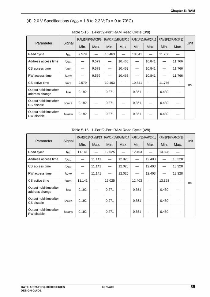
Chapter 5: RAM
(4) 2.0 V Specifications (VDD = 1.8 to 2.2 V; Ta = 0 to 70°C)
Table 5-15 1-Port/2-Port RAM Read Cycle (3/8)
Parameter SignalRAM1P9/RAM2P9 RAM1P10/RAM2P10 RAM1P11/RAM2P11 RAM1P12/RAM2P12
UnitMin. Max. Min. Max. Min. Max. Min. Max.
Read cycle tRC 9.579 — 10.463 — 10.841 — 11.766 —
ns
Address access time tACC — 9.579 — 10.463 — 10.841 — 11.766
CS access time tACS — 9.579 — 10.463 — 10.841 — 11.766
RW access time tARW — 9.579 — 10.463 — 10.841 — 11.766
CS active time tRCS 9.579 — 10.463 — 10.841 — 11.766 —
Output hold time after address change
tOH 0.192 — 0.271 — 0.351 — 0.430 —
Output hold time after CS disable
tOHCS 0.192 — 0.271 — 0.351 — 0.430 —
Output hold time after RW disable
tOHRW 0.192 — 0.271 — 0.351 — 0.430 —
Table 5-15 1-Port/2-Port RAM Read Cycle (4/8)
Parameter SignalRAM1P13/RAM2P13 RAM1P14/RAM2P14 RAM1P15/RAM2P15 RAM1P16/RAM2P16
UnitMin. Max. Min. Max. Min. Max. Min. Max.
Read cycle tRC 11.141 — 12.025 — 12.403 — 13.328 —
ns
Address access time tACC — 11.141 — 12.025 — 12.403 — 13.328
CS access time tACS — 11.141 — 12.025 — 12.403 — 13.328
RW access time tARW — 11.141 — 12.025 — 12.403 — 13.328
CS active time tRCS 11.141 — 12.025 — 12.403 — 13.328 —
Output hold time after address change
tOH 0.192 — 0.271 — 0.351 — 0.430 —
Output hold time after CS disable
tOHCS 0.192 — 0.271 — 0.351 — 0.430 —
Output hold time after RW disable
tOHRW 0.192 — 0.271 — 0.351 — 0.430 —
GATE ARRAY S1L60000 SERIES EPSON 85DESIGN GUIDE
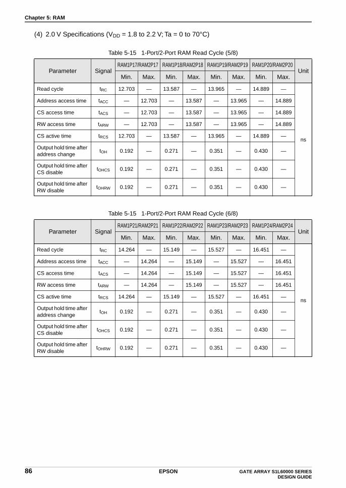
Chapter 5: RAM
(4) 2.0 V Specifications (VDD = 1.8 to 2.2 V; Ta = 0 to 70°C)
Table 5-15 1-Port/2-Port RAM Read Cycle (5/8)
Parameter SignalRAM1P17/RAM2P17 RAM1P18/RAM2P18 RAM1P19/RAM2P19 RAM1P20/RAM2P20
UnitMin. Max. Min. Max. Min. Max. Min. Max.
Read cycle tRC 12.703 — 13.587 — 13.965 — 14.889 —
ns
Address access time tACC — 12.703 — 13.587 — 13.965 — 14.889
CS access time tACS — 12.703 — 13.587 — 13.965 — 14.889
RW access time tARW — 12.703 — 13.587 — 13.965 — 14.889
CS active time tRCS 12.703 — 13.587 — 13.965 — 14.889 —
Output hold time after address change
tOH 0.192 — 0.271 — 0.351 — 0.430 —
Output hold time after CS disable
tOHCS 0.192 — 0.271 — 0.351 — 0.430 —
Output hold time after RW disable
tOHRW 0.192 — 0.271 — 0.351 — 0.430 —
Table 5-15 1-Port/2-Port RAM Read Cycle (6/8)
Parameter SignalRAM1P21/RAM2P21 RAM1P22/RAM2P22 RAM1P23/RAM2P23 RAM1P24/RAM2P24
UnitMin. Max. Min. Max. Min. Max. Min. Max.
Read cycle tRC 14.264 — 15.149 — 15.527 — 16.451 —
ns
Address access time tACC — 14.264 — 15.149 — 15.527 — 16.451
CS access time tACS — 14.264 — 15.149 — 15.527 — 16.451
RW access time tARW — 14.264 — 15.149 — 15.527 — 16.451
CS active time tRCS 14.264 — 15.149 — 15.527 — 16.451 —
Output hold time after address change
tOH 0.192 — 0.271 — 0.351 — 0.430 —
Output hold time after CS disable
tOHCS 0.192 — 0.271 — 0.351 — 0.430 —
Output hold time after RW disable
tOHRW 0.192 — 0.271 — 0.351 — 0.430 —
86 EPSON GATE ARRAY S1L60000 SERIES DESIGN GUIDE

Chapter 5: RAM
(4) 2.0 V Specifications (VDD = 1.8 to 2.2 V; Ta = 0 to 70°C)
Table 5-15 1-Port/2-Port RAM Read Cycle (7/8)
Parameter SignalRAM1P25/RAM2P25 RAM1P26/RAM2P26 RAM1P27/RAM2P27 RAM1P28/RAM2P28
UnitMin. Max. Min. Max. Min. Max. Min. Max.
Read cycle tRC 15.826 — 16.711 — 17.089 — 18.013 —
ns
Address access time tACC — 15.826 — 16.711 — 17.089 — 18.013
CS access time tACS — 15.826 — 16.711 — 17.089 — 18.013
RW access time tARW — 15.826 — 16.711 — 17.089 — 18.013
CS active time tRCS 15.826 — 16.711 — 17.089 — 18.013 —
Output hold time after address change
tOH 0.192 — 0.271 — 0.351 — 0.430 —
Output hold time after CS disable
tOHCS 0.192 — 0.271 — 0.351 — 0.430 —
Output hold time after RW disable
tOHRW 0.192 — 0.271 — 0.351 — 0.430 —
Table 5-15 1-Port/2-Port RAM Read Cycle (8/8)
Parameter SignalRAM1P29/RAM2P29 RAM1P30/RAM2P30 RAM1P31/RAM2P31 RAM1P32/RAM2P32
UnitMin. Max. Min. Max. Min. Max. Min. Max.
Read cycle tRC 17.388 — 18.272 — 18.651 — 19.575 —
ns
Address access time tACC — 17.388 — 18.272 — 18.651 — 19.575
CS access time tACS — 17.388 — 18.272 — 18.651 — 19.575
RW access time tARW — 17.388 — 18.272 — 18.651 — 19.575
CS active time tRCS 17.388 — 18.272 — 18.651 — 19.575 —
Output hold time after address change
tOH 0.192 — 0.271 — 0.351 — 0.430 —
Output hold time after CS disable
tOHCS 0.192 — 0.271 — 0.351 — 0.430 —
Output hold time after RW disable
tOHRW 0.192 — 0.271 — 0.351 — 0.430 —
GATE ARRAY S1L60000 SERIES EPSON 87DESIGN GUIDE

Chapter 5: RAM
(4) 2.0 V Specifications (VDD = 1.8 to 2.2 V; Ta = 0 to 70°C)
Table 5-16 1-Port/2-Port RAM Write Cycle (1/8)
Parameter SignalRAM1P1/RAM2P1 RAM1P2/RAM2P2 RAM1P3/RAM2P3 RAM1P4/RAM2P4
UnitMin. Max. Min. Max. Min. Max. Min. Max.
Write cycle tWC 4.560 — 6.016 — 7.474 — 8.930 —
ns
Write pulse width tWP 2.580 — 4.036 — 5.494 — 6.950 —
CS active time tWCS 2.580 — 4.036 — 5.494 — 6.950 —
Address setup time tAS 0.661 — 0.661 — 0.661 — 0.661 —
Address hold time tAH 1.319 — 1.319 — 1.319 — 1.319 —
Data setup time tDS 0.000 — 0.000 — 0.000 — 0.000 —
Data hold time tDH 2.516 — 3.522 — 4.529 — 5.535 —
Table 5-16 1-Port/2-Port RAM Write Cycle (2/8)
Parameter SignalRAM1P5/RAM2P5 RAM1P6/RAM2P6 RAM1P7/RAM2P7 RAM1P8/RAM2P8
UnitMin. Max. Min. Max. Min. Max. Min. Max.
Write cycle tWC 4.750 — 6.206 — 7.664 — 9.120 —
ns
Write pulse width tWP 2.677 — 4.133 — 5.591 — 7.047 —
CS active time tWCS 2.677 — 4.133 — 5.591 — 7.047 —
Address setup time tAS 0.754 — 0.754 — 0.754 — 0.754 —
Address hold time tAH 1.319 — 1.319 — 1.319 — 1.319 —
Data setup time tDS 0.000 — 0.000 — 0.000 — 0.000 —
Data hold time tDH 2.603 — 3.609 — 4.616 — 5.623 —
88 EPSON GATE ARRAY S1L60000 SERIES DESIGN GUIDE

Chapter 5: RAM
(4) 2.0 V Specifications (VDD = 1.8 to 2.2 V; Ta = 0 to 70°C)
Table 5-16 1-Port/2-Port RAM Write Cycle (3/8)
Parameter SignalRAM1P9/RAM2P9 RAM1P10/RAM2P10 RAM1P11/RAM2P11 RAM1P12/RAM2P12
UnitMin. Max. Min. Max. Min. Max. Min. Max.
Write cycle tWC 4.969 — 6.424 — 7.882 — 9.338 —
ns
Write pulse width tWP 2.802 — 4.257 — 5.715 — 7.171 —
CS active time tWCS 2.802 — 4.257 — 5.715 — 7.171 —
Address setup time tAS 0.848 — 0.848 — 0.848 — 0.848 —
Address hold time tAH 1.319 — 1.319 — 1.319 — 1.319 —
Data setup time tDS 0.000 — 0.000 — 0.000 — 0.000 —
Data hold time tDH 2.691 — 3.697 — 4.704 — 5.710 —
Table 5-16 1-Port/2-Port RAM Write Cycle (4/8)
Parameter SignalRAM1P13/RAM2P13 RAM1P14/RAM2P14 RAM1P15/RAM2P15 RAM1P16/RAM2P16
UnitMin. Max. Min. Max. Min. Max. Min. Max.
Write cycle tWC 5.214 — 6.670 — 8.128 — 9.584 —
ns
Write pulse width tWP 2.953 — 4.409 — 5.867 — 7.323 —
CS active time tWCS 2.953 — 4.409 — 5.867 — 7.323 —
Address setup time tAS 0.942 — 0.942 — 0.942 — 0.942 —
Address hold time tAH 1.319 — 1.319 — 1.319 — 1.319 —
Data setup time tDS 0.000 — 0.000 — 0.000 — 0.000 —
Data hold time tDH 2.778 — 3.784 — 4.791 — 5.798 —
GATE ARRAY S1L60000 SERIES EPSON 89DESIGN GUIDE

Chapter 5: RAM
(4) 2.0 V Specifications (VDD = 1.8 to 2.2 V; Ta = 0 to 70°C)
Table 5-16 1-Port/2-Port RAM Write Cycle (5/8)
Parameter SignalRAM1P17/RAM2P17 RAM1P18/RAM2P18 RAM1P19/RAM2P19 RAM1P20/RAM2P20
UnitMin. Max. Min. Max. Min. Max. Min. Max.
Write cycle tWC 5.418 — 6.873 — 8.331 — 9.788 —
ns
Write pulse width tWP 3.058 — 4.513 — 5.971 — 7.428 —
CS active time tWCS 3.058 — 4.513 — 5.971 — 7.428 —
Address setup time tAS 1.041 — 1.041 — 1.041 — 1.041 —
Address hold time tAH 1.319 — 1.319 — 1.319 — 1.319 —
Data setup time tDS 0.000 — 0.000 — 0.000 — 0.000 —
Data hold time tDH 2.854 — 3.860 — 4.867 — 5.874 —
Table 5-16 1-Port/2-Port RAM Write Cycle (6/8)
Parameter SignalRAM1P21/RAM2P21 RAM1P22/RAM2P22 RAM1P23/RAM2P23 RAM1P24/RAM2P24
UnitMin. Max. Min. Max. Min. Max. Min. Max.
Write cycle tWC 5.635 — 7.091 — 8.549 — 10.005 —
ns
Write pulse width tWP 3.181 — 4.637 — 6.095 — 7.551 —
CS active time tWCS 3.181 — 4.637 — 6.095 — 7.551 —
Address setup time tAS 1.135 — 1.135 — 1.135 — 1.135 —
Address hold time tAH 1.319 — 1.319 — 1.319 — 1.319 —
Data setup time tDS 0.000 — 0.000 — 0.000 — 0.000 —
Data hold time tDH 2.940 — 3.946 — 4.953 — 5.959 —
90 EPSON GATE ARRAY S1L60000 SERIES DESIGN GUIDE

Chapter 5: RAM
(4) 2.0 V Specifications (VDD = 1.8 to 2.2 V; Ta = 0 to 70°C)
Table 5-16 1-Port/2-Port RAM Write Cycle (7/8)
Parameter SignalRAM1P25/RAM2P25 RAM1P26/RAM2P26 RAM1P27/RAM2P27 RAM1P28/RAM2P28
UnitMin. Max. Min. Max. Min. Max. Min. Max.
Write cycle tWC 5.853 — 7.309 — 8.767 — 10.223 —
ns
Write pulse width tWP 3.304 — 4.760 — 6.218 — 7.674 —
CS active time tWCS 3.304 — 4.760 — 6.218 — 7.674 —
Address setup time tAS 1.230 — 1.230 — 1.230 — 1.230 —
Address hold time tAH 1.319 — 1.319 — 1.319 — 1.319 —
Data setup time tDS 0.000 — 0.000 — 0.000 — 0.000 —
Data hold time tDH 3.025 — 4.031 — 5.038 — 6.044 —
Table 5-16 1-Port/2-Port RAM Write Cycle (8/8)
Parameter SignalRAM1P29/RAM2P29 RAM1P30/RAM2P30 RAM1P31/RAM2P31 RAM1P32/RAM2P32
UnitMin. Max. Min. Max. Min. Max. Min. Max.
Write cycle tWC 6.071 — 7.527 — 8.985 — 10.441 —
ns
Write pulse width tWP 3.427 — 4.883 — 6.341 — 7.797 —
CS active time tWCS 3.427 — 4.883 — 6.341 — 7.797 —
Address setup time tAS 1.325 — 1.325 — 1.325 — 1.325 —
Address hold time tAH 1.319 — 1.319 — 1.319 — 1.319 —
Data setup time tDS 0.000 — 0.000 — 0.000 — 0.000 —
Data hold time tDH 3.110 — 4.116 — 5.123 — 6.130 —
GATE ARRAY S1L60000 SERIES EPSON 91DESIGN GUIDE
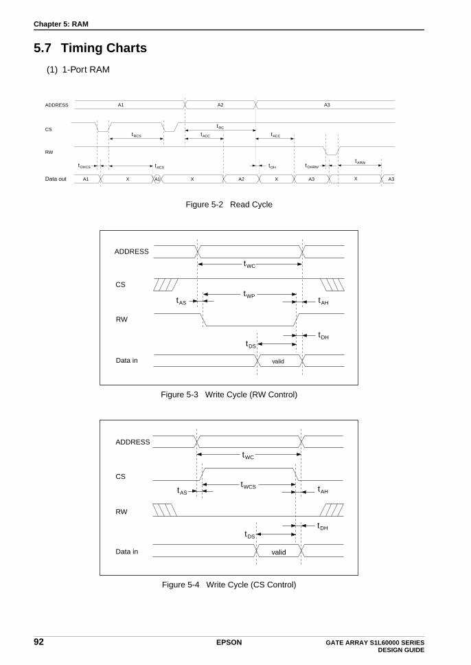
Chapter 5: RAM
5.7 Timing Charts
(1) 1-Port RAM
Figure 5-2 Read Cycle
Figure 5-3 Write Cycle (RW Control)
Figure 5-4 Write Cycle (CS Control)
tOH
X X XX
tOHCS tACS
tACC tACC
tOHRW
tARW
A1 A2 A3ADDRESS
CS
RW
Data out
tRCS
tRC
A1 A1 A2 A3 A3
tWC
tAS
tWP
tDH
tAH
ADDRESS
CS
RW
Data in valid
tDS
tWC
tAStWCS
tDH
tAH
ADDRESS
CS
RW
Data in valid
tDS
92 EPSON GATE ARRAY S1L60000 SERIES DESIGN GUIDE

Chapter 5: RAM
(2) 2-Port RAM
Figure 5-5 Read Cycle
Figure 5-6 Write Cycle (WR Control)
Figure 5-7 Write Cycle (CS Control)
tOH
X X XX
tOHCS tACS
tACC tACC
tOHRW
tARW
A1 A2 A3ADDRESS
CS
RD
Data out
tRCS
tRC
A1 A1 A2 A3 A3
tWC
tAS
tWP
tDH
tAH
ADDRESS
CS
WR
Data in valid
tDS
tWC
tAS
tWCS
tDH
tAH
ADDRESS
CS
WR
Data in valid
tDS
GATE ARRAY S1L60000 SERIES EPSON 93DESIGN GUIDE
Chapter 5: RAM
5.8 RAM Test Method
When it comes to internal RAM, specialized tests are performed corresponding to the RAM structure, separate from the ramdom logic. Please structure test circuits which facilitate direct access to the internal RAM from external pins for this purpose. See Section 6.3 of Chapter 6 regarding the method of structuring the RAM test circuits.
Also, although EPSON will generate an independent test pattern for the RAM, the customer should provide a RAM test pattern template.
5.9 Estimating RAM Current Consumption
• The method for estimating the current consumption at VDD (Typ.) = 2.5 V is given below.
(Both the 1-port and 2-port RAMs can be estimated as follows:)
At standby (CS = 0) : 0 [µA]
During operation (CS = 1): [(-1×10⁻⁵ W2 + 0.0156 W + 2.1126) + (0.0023 W + 0.2197)Y] × f [µA]
W : Number of words Y : Number of Bits f : MHz (average access cycles)
• The method for estimating the current consumption at VDD (Typ.) = 2.0 V is given below.
(Both the 1-port and 2-port RAMs can be estimated as follows:)
At standby (CS = 0) : 0 [µA]
During operation (CS = 1): [(-1×10⁻⁵ W2 + 0.0117 W + 1.4513) + (0.0015 W + 0.1914)Y] × f [µA]
W : Number of words Y : Number of Bits f : MHz (average access cycles)
94 EPSON GATE ARRAY S1L60000 SERIES DESIGN GUIDE

Chapter 5: RAM
5.10 RAM Symbols and How They Are Used
All simulation models have not been prepared in the RAM logic library using performance characteristics indicative of the RAM word/bit configuration. Therefore, when using the RAM logic library, apply the following methods:
(1) Select a cell (model) from Tables 5-1 and 5-2 depending on the needed word/bit size.
(2) Allocate the selected cell to the circuit and tie any unused input pins to the Low side. Do not connect the unused output pins to anything.
For example, when using 1 port RAM of 16 words multiplied by 8 bits, select the cell (model) of RAM1P1 from table 5-1. Tie its unused input pins to the Low side as Figure 5-8 and configure the circuit according to the required RAM size.
Figure 5-8 Example of the Use of RAM Logic Library (RAM1P1: 16 words × 8 Bits)
RW
CS
A0
A2
A3
A4
D0D1D2D3D4D5D6D7D8
D15
Y0Y1Y2Y3Y4Y5Y6Y7Y8
Y15
RAM1P1
A1
ApplicationCircuit
ApplicationCircuit
GATE ARRAY S1L60000 SERIES EPSON 95DESIGN GUIDE

Chapter 6: Circuit Design Taking Testability Into Account
Chapter 6 Circuit Design Taking Testability Into Account
Before a gate array is shipped the product is tested using an LSI tester. It is necessary to design the circuit keeping testability in mind to facilitate this testing. When designing the circuit, the following points should be carefully considered.
6.1 Considerations Regarding Circuit Initialization
When testing ICs using an LSI tester, or when verifying circuit functionality using a software simulator, the initial state of all FF (Flip Flop) is X (unknown). Consequently, very large test patterns may be necessary, depending on the circuit structure, to initialize the sequential elements or it may not be possible to initialize the circuits at all. Because of this, the circuits should be structured to facilitate easy initialization when they are designed (for example, by using FFs which have reset).
6.2 Considerations Regarding Compressing the Test Patterns
As the gate densities of circuits increase, there is a tendency for test patterns to become larger as well. However, one must understand that there are constraints, such as shown below, to the LSI device tests.
Number of events per test pattern: 256 K events or lessNumber of test patterns: 30 test patterns or lessTotal number of test pattern events: 1 M events or less
These event and test pattern constraints include the test patterns for test patterns for DC testing, test patterns for Z test circuits, and it includes the test pattern for ROM and megabyte- cell prepared by EPSON. Contact our sales office for the number of test patterns for ROM and megabyte cells. Although the RAM test patterns prepared by a customer are restricted, there is no restriction on the full test pattern prepared by EPSON.
When designing, please structure circuits in such a way as to increase the testability of the circuit (and to allow the compression of the test patterns), using methods such as including test pins which allow the input of clocks between the counter stages and adding test pins by which to monitor internal signals.
96 EPSON GATE ARRAY S1L60000 SERIES DESIGN GUIDE

Chapter 6: Circuit Design Taking Testability Into Account
6.3 Test Circuit Which Simplifies AC and DC Testing
The S1L60000 Series requires to add test circuits so that DC testing and AC testing can be done efficiently at the shipment.
If the customer experiences difficulties while adding test circuitry, then the customer should contact EPSON.
6.3.1 Test Circuit Structure
Figure 6-2 shows a typical DC/AC test circuit and a 2 word x 2 bit (this configuration is for illustrative purposes only) RAM test circuit. This figure and (1)–(4) below should be referenced when designing test circuits. Recommended test circuit control and monitor pin configurations are shown below. If the test circuit includes RAM or functional cell, please refer to Sections 6.4 RAM Test Circuit and 6.5 Functional Cell Test Circuits, as well.
(1) Test Circuit Control and Monitor Pins
Please add or select the following 4 types of test pins.
• Test enable pin: 1 pin
• Test mode select input pin: 4 pins
• Monitor output pin for AC testing: 1 pin
• Monitor output pin for DC testing: 1 pin(Input voltage level)
Table 6-1 Test Terminal Constraints
Test Pin TypeNumber of
PinsName of Pins
(row)Constraints, Notes, Etc.
Test Enable Pin 1 pin TSTENDedicated input pinUse ITST1 as input buffer.H: Test mode L: Normal mode
Test Mode Select Input Pins
4 terminals
INP0INP1INP2INP3
May be shared with existing input pin. Do not share with an input pin associated with a critical path.
Monitor output pin for AC testing
1 pin OUT3
May be shared with existing I/O buffers. Do not share with a bidirectional, 3-state terminal or with an N-channel open-drain cell. Type S and Type M are not available.
Monitor output pin for DC testing
1 pin OUT4
May be shared with existing I/O buffers. Do not share with a bidirectional, 3-state terminal or with an N-channel open-drain cell.
Output pins and input/output pins
— — Uses I/O buffers with test mode select.
GATE ARRAY S1L60000 SERIES EPSON 97DESIGN GUIDE

Chapter 6: Circuit Design Taking Testability Into Account
• DC Test
Measurements are performed to insure that all input and output pins adhere to DC characteristic specifications. When test circuitry is not implemented, it is necessary for the customer to generate test patterns by which the DC characteristics can be measured. The amount of work in generating the test patterns may increase dramatically when there are no test circuits.
The task of generating test patterns and measuring the DC chracteristics is simplifiedby using test circuits.
• AC Testing
AC testing is a pin-to-pin (i.e. input pin to output pin) delay measurement. If device testing is not performed at actual operating frequency, device performance is assured through delay measurements along specific paths.
Also, the AC test monitor output pin is used to evaluate the variance between lots in the manufacturing process by measuring a defined AC path. The recommended test circuit “TCIR2” measures the difference between a delay in delay cells and a delay when they are bypassed; this enables delay measurements to be performed regardless of the test circuit placement inside the chip or measurement conditions external to the chip.
(2) Adding the Test Mode Control Circuit
a. Please utilize the test mode control circuit (TCIR2).
b. The X output pins of the input buffer (ITST1) of the test-mode selector pins should be connected to the TST input pin and ILG input pin of TCIR2, respectively.
c. The output of the input buffer of the test-mode selection input pins should be connected to the input pins of the TCIR2.
The output of the input buffer of INP0 should be connected to the TM0 pin of the TCIR2.
The output of the input buffer of INP1 should be connected to the TM1 pin of the TCIR2.
The output of the input buffer of INP2 should be connected to the TM2 pin of the TCIR2.
The output of the input buffer of INP3 should be connected to the TM2 pin of the TCIR2.
d. The output pins of the test-mode control circuit (TCIR2) should be connected to the input pins of the input/output buffers.
The output pin (TAC) of the TCIR2 should be connected to the TA pins of the input/output buffers of the AC test-monitoring output pin (OUT3).
The output pin (TS) of the TCIR2 should be connected to the TS pins of all input/output buffers.
The output pin (TD) of the TCIR2 should be connected to the TA pins of all input/output buffers, not including those of the test-monitoring output pins (OUT3 and OUT4).
The output pin (TE) of the TCIR2 should be connected to the TE pins of the input/output buffers of the 3-state pin (OUT2) and bi-directional pin (BID1).
The output pin (OLG) of the TCIR2 should be connected to the TA pins of the input/output buffers of the DC test-monitoring output pin (OUT4).
e. Use the TCIR2 output pin (MS) for macro control in cases involving RAM and functional cells.
98 EPSON GATE ARRAY S1L60000 SERIES DESIGN GUIDE
Chapter 6: Circuit Design Taking Testability Into Account
f. Adjust the signals connecting to the TA, TE, and TS pins of the input/output buffers to avoid exceeding fan-out limits.
(3) Setting the Test Mode
a. DC Test
• Quiescent Current Measurement Mode
TSTEN . . . High
• Output Characteristics (VOH/VOL) Measurement Mode
TSTEN . . . HighINP0 . . . HighINP1 . . . High and LowINP2 . . . LowINP3 . . . High and LowMeasurement pin *1 . . . High and Low
*1. Apply to all output and all bi-directional pins except the DC test monitor pins.
• Input Characteristics (VIH/VIL) Measurement Mode
TSTEN . . . HighMeasurement pin *2 . . . HighNon-measured pin . . . HighDC test monitor pin . . . High and Low
*2. Apply to all input and all bi-directional pins except TSTEN.
• Leakage current measurement mode
TSTEN . . . High and LowINP0 . . . High and LowINP1 . . . LowINP2 . . . HighINP3 . . . High and LowMeasured pin *3 . . . High and LowTri-state and open-drain pins . . . High impedance
*3. Apply to all input, all 3-state output, and all bi-directional pins except TSTEN and INP0-2.
b. Dedicated AC test
• Dedicated AC Path Measurement Mode
TSTEN . . . HighINP0 . . . LowINP1 . . . LowINP2 . . . Change to High and change to LowINP3 . . . High (delay cell delay) and low
(bypass delay)AC test monitor pin . . . High and Low
GATE ARRAY S1L60000 SERIES EPSON 99DESIGN GUIDE
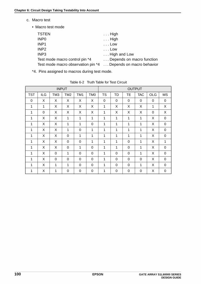
Chapter 6: Circuit Design Taking Testability Into Account
c. Macro test
• Macro test mode
TSTEN . . . HighINP0 . . . HighINP1 . . . LowINP2 . . . LowINP3 . . . High and LowTest mode macro control pin *4 . . . Depends on macro functionTest mode macro observation pin *4 . . . Depends on macro behavior
*4. Pins assigned to macros during test mode.
Table 6-2 Truth Table for Test Circuit
INPUT OUTPUT
TST ILG TM3 TM2 TM1 TM0 TS TD TE TAC OLG MS
0 X X X X X 0 0 0 0 0 0
1 1 X X X X 1 X X X 1 X
1 0 X X X X 1 X X X 0 X
1 X X 1 1 1 1 1 1 1 X 0
1 X X 1 1 0 1 1 1 1 X 0
1 X X 1 0 1 1 1 1 1 X 0
1 X X 0 1 1 1 1 1 1 X 0
1 X X 0 0 1 1 1 0 1 X 1
1 X X 0 1 0 1 1 0 1 X 0
1 X 0 1 0 0 1 0 0 1 X 0
1 X 0 0 0 0 1 0 0 0 X 0
1 X 1 1 0 0 1 0 0 1 X 0
1 X 1 0 0 0 1 0 0 0 X 0
100 EPSON GATE ARRAY S1L60000 SERIES DESIGN GUIDE
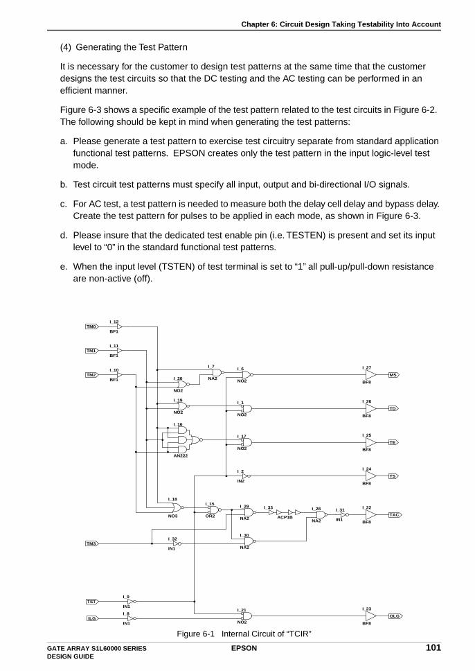
Chapter 6: Circuit Design Taking Testability Into Account
(4) Generating the Test Pattern
It is necessary for the customer to design test patterns at the same time that the customer designs the test circuits so that the DC testing and the AC testing can be performed in an efficient manner.
Figure 6-3 shows a specific example of the test pattern related to the test circuits in Figure 6-2. The following should be kept in mind when generating the test patterns:
a. Please generate a test pattern to exercise test circuitry separate from standard application functional test patterns. EPSON creates only the test pattern in the input logic-level test mode.
b. Test circuit test patterns must specify all input, output and bi-directional I/O signals.
c. For AC test, a test pattern is needed to measure both the delay cell delay and bypass delay. Create the test pattern for pulses to be applied in each mode, as shown in Figure 6-3.
d. Please insure that the dedicated test enable pin (i.e. TESTEN) is present and set its input level to “0” in the standard functional test patterns.
e. When the input level (TSTEN) of test terminal is set to “1” all pull-up/pull-down resistance are non-active (off).
Figure 6-1 Internal Circuit of “TCIR”
I_33
ACP1B
I_22
BF8
I_23
BF8
I_24
BF8
I_25
BF8
I_26
BF8
I_27
BF8
I_15
OR2
I_16
AN222
I_21
NO2
I_17
NO2
I_1
NO2
I_2
IN2
I_18
NO3
I_6
NO2
I_19
NO2
I_20
NO2
I_28
NA2
I_29
NA2
I_30
NA2
I_7
NA2
I_31
IN1
I_32
IN1
I_9
IN1
I_8
IN1
I_10
BF1
I_11
BF1
I_12
BF1TM0
TM1
TM2 MS
TD
TE
TS
TAC
TM3
TST
OLGILG
GATE ARRAY S1L60000 SERIES EPSON 101DESIGN GUIDE
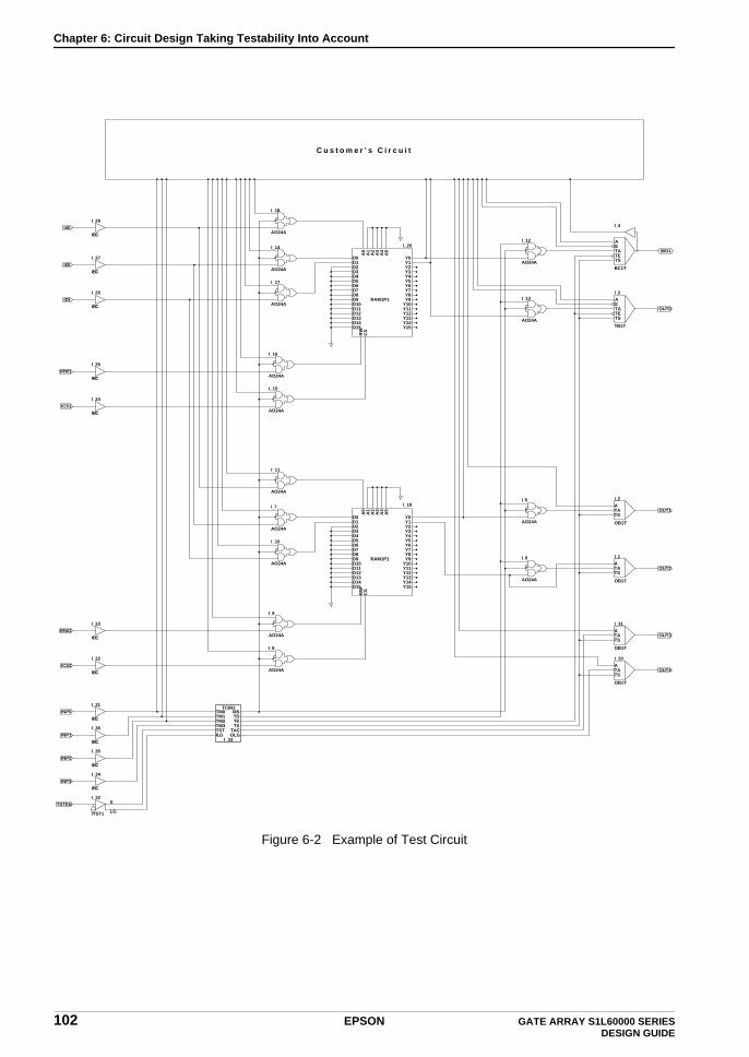
Chapter 6: Circuit Design Taking Testability Into Account
Figure 6-2 Example of Test Circuit
I_32
ITST1
I_33
TCIR2
ILG
TM0TM1TM2TM3TST
MS
OLGTAC
TDTETS
I_30
OB1T
ATATS
I_31
OB1T
ATATS
I_1
OB1T
ATATS
I_2
OB1T
ATATS
I_3
TB1T
AETATETS
I_4
BC1T
AETATETS
I_5
AO24A
I_6
AO24A
I_12
AO24A
I_13
AO24A
I_7
AO24A
I_8
AO24A
I_9
AO24A
I_10
AO24A
I_11
AO24A
I_14
AO24A
I_15
AO24A
I_16
AO24A
I_17
AO24A
I_18
AO24A
I_19
RAM1P1
A0
A1
A2
A3
A4
A5
CS
D0D1
D10D11D12D13D14D15
D2D3D4D5D6D7D8D9
RW
Y0Y1
Y10Y11Y12Y13Y14Y15
Y2Y3Y4Y5Y6Y7Y8Y9
I_20
RAM1P1
A0
A1
A2
A3
A4
A5
CS
D0D1
D10D11D12D13D14D15
D2D3D4D5D6D7D8D9
RW
Y0Y1
Y10Y11Y12Y13Y14Y15
Y2Y3Y4Y5Y6Y7Y8Y9
I_34
IBC
I_35
IBC
I_36
IBC
I_21
IBC
I_24
IBC
I_25
IBC
I_26
IBC
I_27
IBC
I_28
IBC
I_22
IBC
I_23
IBC
IA0
BID1
ID0
ID1
OUT0
IRW1
ICS1
OUT1
OUT2
IRW2OUT3
ICS2OUT4
INP0
INP1
INP2
INP3
TSTEN
LG
X
C u s t o m e r ’ s C i r c u i t
102 EPSON GATE ARRAY S1L60000 SERIES DESIGN GUIDE
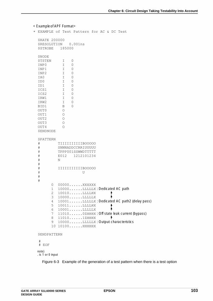
Chapter 6: Circuit Design Taking Testability Into Account
Figure 6-3 Example of the generation of a test pattern when there is a test option
* EXAMPLE of Test Pattern for AC & DC Test
## EOF
$RATE 200000$RESOLUTION 0.001ns$STROBE 185000
$NODE$TSTEN I 0INP0 I 0INP1 I 0INP2 I 0IA0 I 0ID0 I 0ID1 I 0ICS1 I 0ICS2 I 0IRW1 I 0IRW2 I 0BID1 B 0OUT0 OOUT1 OOUT2 OOUT3 OOUT4 O$ENDNODE
$PATTERN# TIIIIIIIIIIBOOOOO# SNNNADDCCRRIUUUUU# TPPP001SSWWDTTTTT# E012 1212101234# N## IIIIIIIIIIIBOOOOO# U## 0 00000......XXXXXX 1 10000......LLLLLX : Dedicated AC path 2 10010......LLLLHX 3 10000......LLLLLX 4 10001......LLLLLX : Dedicated AC path2 (delay pass) 5 10011......LLLLHX 6 10001......LLLLLX 7 11010......0ZHHHX : Off state leak current (bypass) 8 11010......1ZHHHX 9 10000......LLLLLX : Output characteristics 10 10100......HHHHHX
$ENDPATTERN
< Exampleof APF Format>
note). is 1 or 0 input
GATE ARRAY S1L60000 SERIES EPSON 103DESIGN GUIDE
Chapter 6: Circuit Design Taking Testability Into Account
6.4 RAM Test Circuit
When a RAM is used it is necessary to test all bits before shipping the product. RAM terminals must be accessible via primary I/O pins. RAM test circuitry can be implemented, which multiplexes existing pin functionality with direct RAM access functionality so as to avoid increasing the designs pin count.
Also, when multiple RAMs are used, we recommend that each RAM’s pins be accessible via unique I/O pins. However, when the number of external I/O pins is inadequate, each RAM’s pins may share common external I/O pins.
The example test circuit in Figure 6-2 performs normal operations unless in test mode; when placed in test mode, the circuit allows data to be written directly to RAM from external pins ICS, IRW, ID0-1, and IA0. At the same time, RAM output in this circuit can be read out to external pins AY0 and AY1.
Although it is possible to share the RAM pins with bi-directional pins or 3-state output pins, it is necessary to tie the bi-directional pins to either an input or an output state during RAM test. However, please do not allocate an input buffer with a pull-up resistor to CS, because doing so would make it impossible to measure the quiescent current.
6.4.1 RAM Test Patterns
After incorporating RAM test circuitry, it is necessary to make test patterns for both the normal operating state and the test state of the chip. Checks are performed in the normal state to verify the connection with the customer’s circuits, and are performed to insure that the test circuit is correct in the test state. Also, we request a test pattern to serve as a template when EPSON generates the RAM test pattern. See Figures 6-4 and 6-5 for an outline of how to generate this test pattern.
This pattern serves as a template for 1-port RAM tests.
104 EPSON GATE ARRAY S1L60000 SERIES DESIGN GUIDE
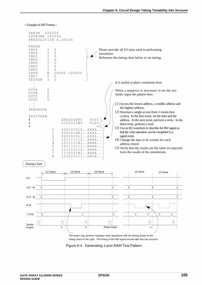
Chapter 6: Circuit Design Taking Testability Into Account
Figure 6-4 Generating 1-port RAM Test Pattern
X
(1) Setup
A [2 : 0]
R W
Y [3:0]
CS
D [3 : 0]
X (Read Data)StrobeExpect
(2) Write (3) Read
X
(2) Write (2) Write
The tester may perform repetitive write operations with the timing shown in the
timing chart on the right. The timing of the RW signal should take this into account.
$RATE 200000$STROBE 185000$RESOLUTION 0.001ns
$NODEINPA I 0INPB I 0INPC I 0INPD I 0INPE I 0INPF I 0INPG I 0INPH N 20000 120000INPI I 0TESTEN I 0
.
.OUTA 0OUTB 0OUTC 0OUTD 0
.
.$ENDNODE
$PATTERN###
AAADDDDRC YYYY0120123WS 0123
0 000101010..XXXX..1 0001010N1..XXXX..2 000101011..HLHL..3 101111110..XXXX..4 1011111N1..XXXX..5 101111111..HHHH..6 111010110..XXXX..7 1110101N1..XXXX..8 111010111..LHLH..
< Example ofAPF Format >
Please provide all I/O pins used in performingsimulation.Reference the timing chart below to set timing.
It is useful to place comments here.
When a sequence is necessary to set the testmode, input the pattern here.
[1]
[2]
[3]
[4]
[5]
Access the lowest address, a middle address andthe highest address.Structure a single access from 3 events (testcycles). In the first event, set the data and theaddress. In the next event, perform a write. In thethird event, perform a read.Use an RZ waveform to describe the RW signal sothat the write operation can be completed in asignal event.
Verify that the results are the same as expectedform the results of the simulations.
Timing Chart
Change the data to be written for eachaddress tested.
GATE ARRAY S1L60000 SERIES EPSON 105DESIGN GUIDE
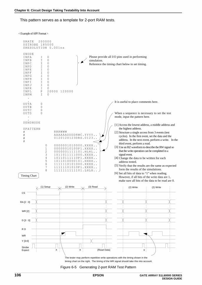
Chapter 6: Circuit Design Taking Testability Into Account
This pattern serves as a template for 2-port RAM tests.
Figure 6-5 Generating 2-port RAM Test Pattern
< Example ofAPF Format >
Please provide all I/O pins used in performingsimulation.Reference the timing chart below to set timing.
It is useful to place comments here.
When a sequence is necessary to set the testmode, input the pattern here.
[1]
[2]
[3]
[4]
[5]
Access the lowest address, a middle address andthe highest address.Structure a single access from 3 events (testcycles). In the first event, set the data and the address. In the next event, perform a write. In thethird event, perform a read.Use an RZ waveform to describe the RW signal sothat the write operation can be completed in asignal event.
Verify that the results are the same as expectedform the results of the simulations.
Timing Chart
Change the data to be written for eachaddress tested.
[6] SetHowever, if all bits of the write data are 1, make sure all bits of the data to be read are 0.
all bits of data to “1” when reading.
$RATE 200000$STROBE 185000$RESOLUTION 0.001ns
$NODEINPA I 0INPB I 0INPC I 0INPD I 0INPE I 0INPF I 0INPG I 0INPH I 0INPI I 0INPJ I 0INPK I 0INPL P 20000 120000INPM I 0
.
.OUTA 0OUTB 0OUTC 0OUTD 0
.
.$ENDNODE
$PATTERN####
RRRWWWAAAAAADDDDRWC.YYYY..0120120123DRS.0123..
0 0000001010000.XXXX..1 00000010100P1.XXXX..2 0000001111101.HLHL..3 1011011111000.XXXX..4 10110111110P1.XXXX..5 1011010000101.HHHH..6 1111110101000.XXXX..7 11111101010P1.XXXX..8 1111111111101.LHLH..
X
(1) Setup
RA [2 : 0]
WR
Y [3:0]
CS
D [3 : 0]
X (Read Data)StrobeExpect
(2) Write (3) Read
X
R D
(2) Write (2) Write
WR [2]
The tester may perform repetitive write operations with the timing shown in the
timing chart on the right. The timing of the WR signal should take this into account.
106 EPSON GATE ARRAY S1L60000 SERIES DESIGN GUIDE

Chapter 6: Circuit Design Taking Testability Into Account
6.5 Function Cell Test Circuits
When function cells are used, then testing the operation of all circuits (including the user circuits) requires a vast number of test patterns and a great amount of time. It is because of this that it is necessary to design test circuits able to verify the operation of each independent functional cell and user circuit, as was done with the RAM blocks. When designing the test circuits, please keep the following cautions and considerations in mind. For more details, contact EPSON.
6.5.1 Test Circuit Structures
(1) Provide test circuitry which facilitates direct access to all pins of each functional cell via I/O pins. Add a test circuit (connected to a terminal) which isolates each functional cell from the surrounding circuits.
(2) Even when functional cell input pins are fixed to VSS or VDD, design test circuitry which insures access to all functional cell pins.
(3) Even when functional cell output pins are not used, design test circuitry which insures access to all functional cell pins.
(4) Each functional cell pin must be connected to a unique I/O pin.
(5) Do not use sequential elements in the test circuitry for functional cells.
(6) Do not invert the input signal from the test input terminal and input it into the functional cell. Similarly, do not invert the functional cell output signal and output it to the test output terminal.
(7) There is no need to design a test circuit when the functional cell input pins and output pins are directly connected to the IC pins.
6.5.2 Test Patterns
The test patterns can be categorized into the following three types:
1) Test patterns to test only the user’s circuit.
2) Test patterns to test all circuits.
3) Test patterns to test the functional cells only.
Test patterns that the customers generateare of type 1 and 2. Customers are not required to generate test patterns of type 3. EPSON maintains test patterns to be used for type 3.
Please be advised that EPSON will not disclose information pertaining to the functional cell test patterns.
GATE ARRAY S1L60000 SERIES EPSON 107DESIGN GUIDE

Chapter 6: Circuit Design Taking Testability Into Account
6.5.3 Test Circuit Data
Please provide the following information regarding functional test circuitry. This information is required for functional cell testing during simulation and IC device testing.
(1) Please clearly define the I/O pin to functional cell pin connectivity while in test mode.
(2) When the test circuits are structured in such a way that a single test terminal is able to test multiple functional cells, please clearly define the names of the functional cells which can be selected and the type of the test modes, and their relationships.
(3) Please clearly define pass numbers on the names of the functional cells on the drawings, and clearly define the test terminals and their association with functional cells, especially when identical functional cells are used more than once.
(4) Please clearly define the method of switching into test mode.
Please keep in mind to contact to our sales office when using functional cells and refer to “Functional Cells Design Guide”.
108 EPSON GATE ARRAY S1L60000 SERIES DESIGN GUIDE
Chapter 6: Circuit Design Taking Testability Into Account
GATE ARRAY S1L60000 SERIES EPSON 109DESIGN GUIDE

Chapter 7: Propagation Delay and Timing
Chapter 7 Propagation Delay and TimingPropagation delay time is determined by the intrinsic cell delay and by the per-load delay, which is a function of the wire interconnect and fan-in capacitances.
Delay times vary depending upon power supply voltage, ambient temperature, and process conditions. They also vary depending on factors involved in the structure of the circuit, input waveform, input logic level, and the mirror effect.
Post Simulation uses more acculate environment.
Please be advised that delay times may not be equal to the values of delay calculation described below using the values listed in the “Gate Array S1L60000 Series MSI Cell Library”.
7.1 Notes on the relationship between Ta and Tj
The propagation delay of CMOS IC is basically changed by Tj (i.e. temperature at junctions). The IC is specified by Ta. However, the relation between Tj and Ta is not constant, but changes with thermal resistance and power consumption. (Refer to chapter 9.2 for detail.)
In ASIC design, each package and IC power consumption is changed by a circuit and an application. Therefore, it is very difficult to specify according to Ta. Then, in the S1L60000 series, propagation delay libraries are ready for checking at initial design under the following conditions:
* Tj = 0 to 85°C library using for Ta = 0 to 70°C* Tj = -40 to 125°C library using for Ta = -40 to 85°C
When the relation between Ta and Tj is very different from the normal values by estimating the package and application, the Tj = -40 to 125°C library can be used for Ta = 0 to 70°C or other conditions should be considered if necessary.
7.2 Simple Delay Models
Simple propagation delay time tpd can be calculated using the following formula:
tpd = t0 + K × (∑ Load A + Load B)
where, t0: Intrinsic cell delay [ps]K: Load delay coefficient [ps/Lu]Load A: The input load capacitance due to fan-in [Lu]Load B: The interconnect load capacitance [Lu]
Note: The values for t0 and K differ depending upon the operating voltage, the ambient temperature, and the process conditions.
Typical values for t0 and K (VDD = nominal value, Ta = 25°C, and process = nominal value) are found in the “Gate Array S1L60000 Series MSI Cell Library”. Select typical values for T0 and K according to the target power supply voltage.
110 EPSON GATE ARRAY S1L60000 SERIES DESIGN GUIDE
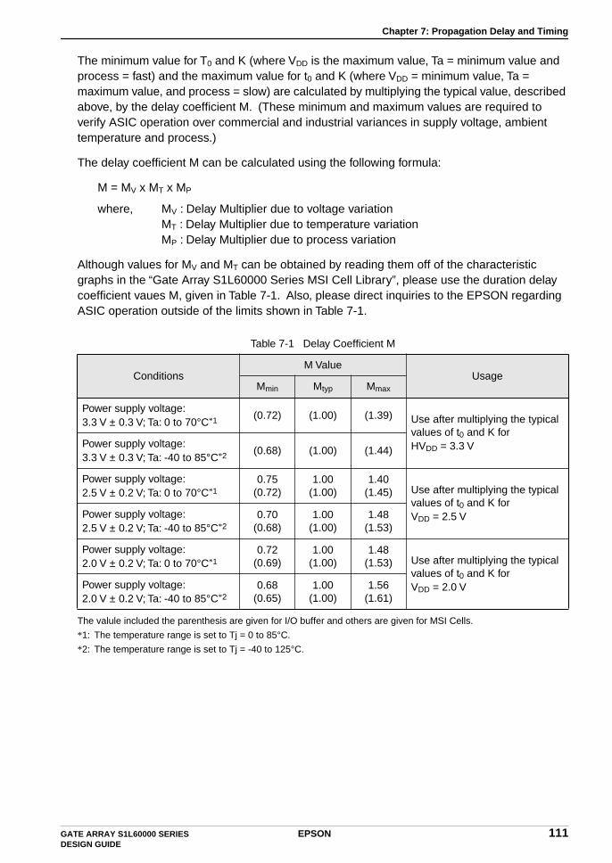
Chapter 7: Propagation Delay and Timing
The minimum value for T0 and K (where VDD is the maximum value, Ta = minimum value and process = fast) and the maximum value for t0 and K (where VDD = minimum value, Ta = maximum value, and process = slow) are calculated by multiplying the typical value, described above, by the delay coefficient M. (These minimum and maximum values are required to verify ASIC operation over commercial and industrial variances in supply voltage, ambient temperature and process.)
The delay coefficient M can be calculated using the following formula:
M = MV x MT x MP
where, MV : Delay Multiplier due to voltage variationMT : Delay Multiplier due to temperature variationMP : Delay Multiplier due to process variation
Although values for MV and MT can be obtained by reading them off of the characteristic graphs in the “Gate Array S1L60000 Series MSI Cell Library”, please use the duration delay coefficient vaues M, given in Table 7-1. Also, please direct inquiries to the EPSON regarding ASIC operation outside of the limits shown in Table 7-1.
The valule included the parenthesis are given for I/O buffer and others are given for MSI Cells.
*1: The temperature range is set to Tj = 0 to 85°C.
*2: The temperature range is set to Tj = -40 to 125°C.
Table 7-1 Delay Coefficient M
ConditionsM Value
UsageMmin Mtyp Mmax
Power supply voltage:3.3 V ± 0.3 V; Ta: 0 to 70°C*1 (0.72) (1.00) (1.39) Use after multiplying the typical
values of t0 and K forHVDD = 3.3 VPower supply voltage:
3.3 V ± 0.3 V; Ta: -40 to 85°C*2 (0.68) (1.00) (1.44)
Power supply voltage:2.5 V ± 0.2 V; Ta: 0 to 70°C*1
0.75(0.72)
1.00(1.00)
1.40(1.45) Use after multiplying the typical
values of t0 and K forVDD = 2.5 VPower supply voltage:
2.5 V ± 0.2 V; Ta: -40 to 85°C*20.70
(0.68)1.00
(1.00)1.48
(1.53)
Power supply voltage:2.0 V ± 0.2 V; Ta: 0 to 70°C*1
0.72(0.69)
1.00(1.00)
1.48(1.53) Use after multiplying the typical
values of t0 and K forVDD = 2.0 VPower supply voltage:
2.0 V ± 0.2 V; Ta: -40 to 85°C*20.68
(0.65)1.00
(1.00)1.56
(1.61)
GATE ARRAY S1L60000 SERIES EPSON 111DESIGN GUIDE
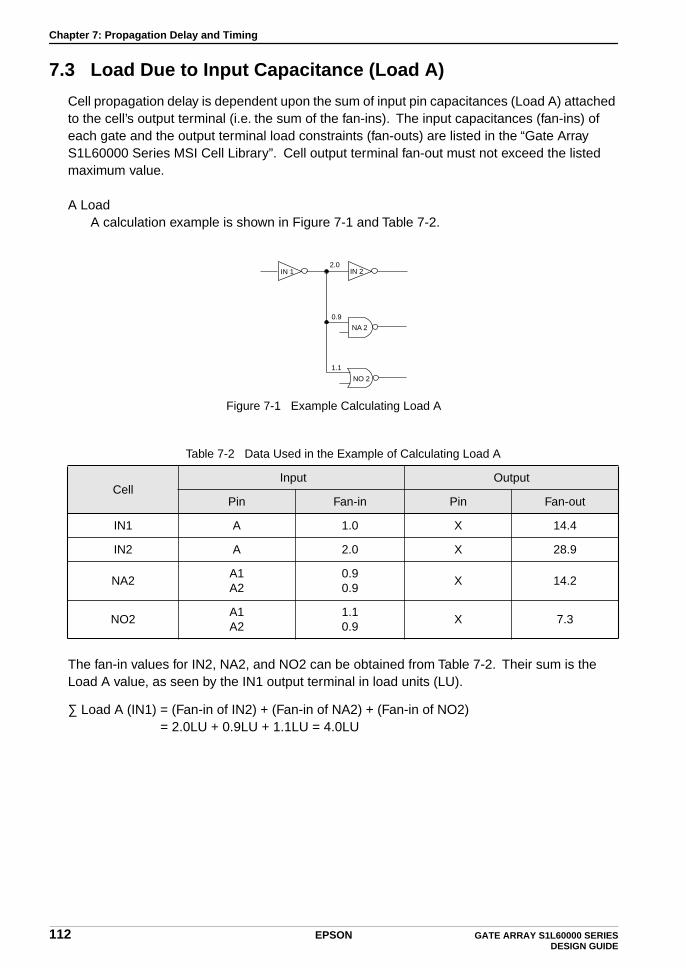
Chapter 7: Propagation Delay and Timing
7.3 Load Due to Input Capacitance (Load A)
Cell propagation delay is dependent upon the sum of input pin capacitances (Load A) attached to the cell’s output terminal (i.e. the sum of the fan-ins). The input capacitances (fan-ins) of each gate and the output terminal load constraints (fan-outs) are listed in the “Gate Array S1L60000 Series MSI Cell Library”. Cell output terminal fan-out must not exceed the listed maximum value.
A LoadA calculation example is shown in Figure 7-1 and Table 7-2.
Figure 7-1 Example Calculating Load A
The fan-in values for IN2, NA2, and NO2 can be obtained from Table 7-2. Their sum is the Load A value, as seen by the IN1 output terminal in load units (LU).
∑ Load A (IN1) = (Fan-in of IN2) + (Fan-in of NA2) + (Fan-in of NO2) = 2.0LU + 0.9LU + 1.1LU = 4.0LU
Table 7-2 Data Used in the Example of Calculating Load A
Cell Input Output
Pin Fan-in Pin Fan-out
IN1 A 1.0 X 14.4
IN2 A 2.0 X 28.9
NA2A1A2
0.90.9
X 14.2
NO2A1A2
1.10.9
X 7.3
IN 1 IN 2
NA 2
NO 2
2.0
0.9
1.1
112 EPSON GATE ARRAY S1L60000 SERIES DESIGN GUIDE

Chapter 7: Propagation Delay and Timing
7.4 Load Due to Interconnect Capacitance (Load B)
The load resulting from the capacitance of the interconnect between cells (Load B) cannot be accurately calculated until the ASIC layout has been performed. However, Load B is correlated with the number of branches (number of nodes) connected to the wire, so it is possible to statistically estimate the Load B value. The estimated interconnect capacitance for each master is listed in the “Gate Array S1L60000 Series MSI Cell Library”.
7.5 Propagation Delay Calculations
Below we present a sample propagation delay time calculation using the circuit shown in Figure 7-2 (assume an operating voltage of 2.5 V) and the data of Table 7-3.
Figure 7-2 Circuit for the Sample Calculation of the Propagation Delay Time
Table 7-3 Characteristics (Power Supply Voltage = 2.5 V)
CellInput Output tpd (Typ.)
Pin Fan-in Pin Fan-out From To Edge t0 (ps) K (ps/LU)
IN1 A 1.0 X 14.4 A X43 18.7
44 10.2
IN2 A 2.0 X 28.9 A X36 9.3
37 5.1
NA2 A1 0.9 X 14.2 A X57 18.7
50 16.0
NO2 A1 1.1 X 7.3 A X56 36.0
53 10.2
NO 2
A
P
B
C
D
IN 1 IN 2
NA 2
0.9
1.1
2.0
GATE ARRAY S1L60000 SERIES EPSON 113DESIGN GUIDE

Chapter 7: Propagation Delay and Timing
For this example, assume that Load B of NODE P = 2 (LU), and assume that Load B of Nodes B, C and D = 0 (LU). Also, note that propagation delay varies depending on the output terminal state transition (rising or falling edge). Below please find examples calculating the propagation delays for paths A to P, A to B, A to C and A to D for both rising and falling cases under typical operating conditions at 3.3 V.
1. PATH A to P: tpd = tpd (IN1)tpd (Arising to Pfalling) = t0 + K × (Load A + Load B)
= 44 + 10.2 × (4.0 + 2)= 105.20(ps)
tpd (Arising to Pfalling) = t0 + K × (Load A + Load B)= 43 + 18.7 × (4.0 + 2)= 155.20(ps)
2. PATH A to B: tpd = tpd (IN1) + tpd (IN2)tpd (Arising to Brising) = tpd (Arising to Pfalling) + tpd (Pfalling to Brising)
= 105.20 + t0= 105.20 + 36= 141.20(ps)
tpd (Afalling to Bfalling) = tpd (Afalling to Prising) + tpd (Prising to Bfalling)= 155.20 + t0= 155.20 + 37= 192.20(ps)
3. PATH A to C: tpd = tpd (IN1) + tpd (NA2)tpd (Arising to Crising) = tpd (Arising to Pfalling) + tpd (Pfalling to Crising)
= 105.20 + t0= 105.20 + 57= 162.20(ps)
tpd (Afalling to Cfalling) = tpd (Afalling to Prising) + tpd (Prising to Cfalling)= 155.20 + t0= 155.20 + 50= 205.20(ps)
4. PATH A to D: tpd = tpd (IN1) + tpd (NO2)tpd (Arising to Drising) = tpd (Arising to Pfalling) + tpd (Pfalling to Drising)
= 105.20 + t0= 105.20 + 56= 161.20(ps)
tpd (Afalling to Dfalling) = tpd (Afalling to Prising) + tpd (Prising to Dfalling)= 155.20 + t0= 155.20 + 53= 208.20(ps)
114 EPSON GATE ARRAY S1L60000 SERIES DESIGN GUIDE
Chapter 7: Propagation Delay and Timing
7.6 Calculating Output Buffer Delay
Assuming that the load capacitance connected to the output buffer is CL, the delay time tpd is calculated as follows:
tpd = t0 (Output cell) + K (Output cell) × CL/10
t0 (Output cell) : The intrinsic delay of the output cell [ps]K (Output cell) : The output cell load delay coefficient [ps/10 pF]CL : The load capacitance connected [pF]
Please reference the “Gate Array S1L60000 Series MSI Cell Library” regarding the intrinsic delays and load delay coefficients of the output cells and pre-drivers.
7.7 Sequential Buffer Setup/Hold Time
A critical factor to analyze when designing an ASIC is sequential cell usage and operation. Data which is to be stored by sequential logic must arrive before the gating or clock signal to insure sufficient data setup and proper operation. That same data must remain unchanged or held subsequent to the gating or clock signal. These timing rules and others (see below) must be taken into consideration when designing sequential logic. Sequential cell specific timing values can be found in the “Gate Array S1L60000 Series MSI Cell Library”.
(1) Minimum Pulse Width: TPWC, TPWS or TPWR
The minimum pulse width refers to the minimum value of the time between a leading edge and a trailing edge of an input pulse waveform, as seen at the clock, set, preset or reset terminal of a sequential cell. Circuit malfunction may occur when a narrow pulse is applied which volates this constraint.
The minimum pulse widths may be of the following three types:
• Clock signal minimum pulse width violation.
• Set signal minimum pulse width violation.
• Reset signal minimum pulse width violation.
(2) Setup Time:
“Setup time” refers to the required time interval in which the data state must be set before the active edge transition of the gate or clock signal in order to correctly store the data in a sequential cell or an MSI function which is made up of sequential cells.
(3) Hold Time:
“Hold time” refers to the required time interval in which the data state must be held after the active edge of the gate or clock signal in order to correctly store the data in a sequential cell or an MSI function which is made up of sequential cells.
GATE ARRAY S1L60000 SERIES EPSON 115DESIGN GUIDE
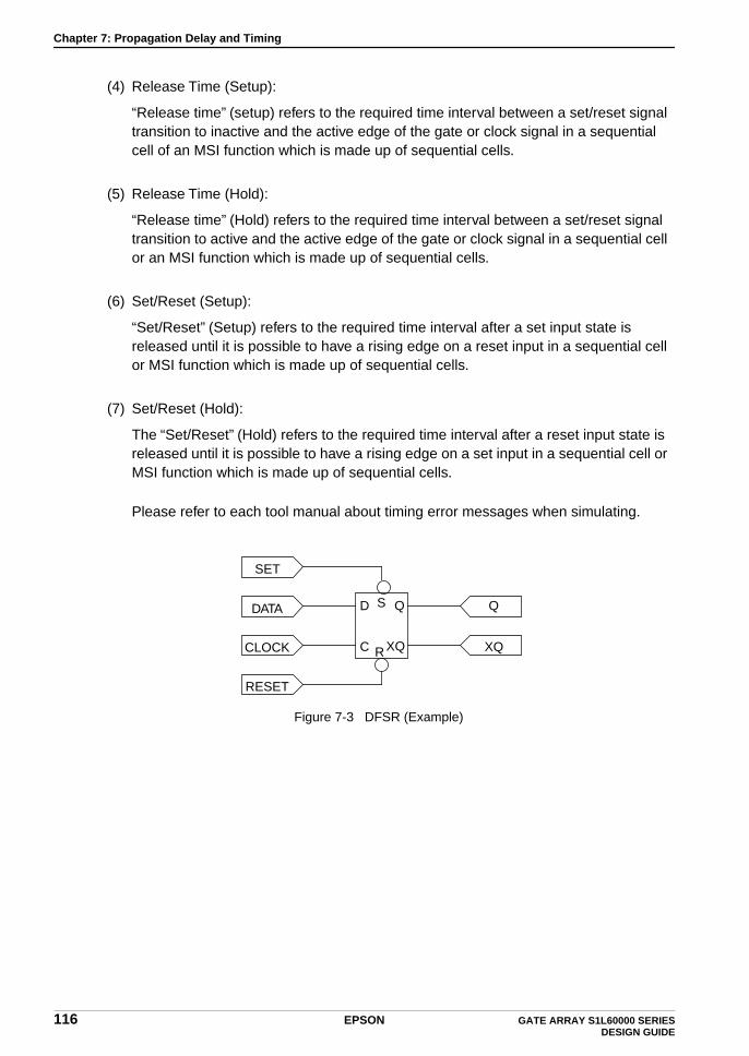
Chapter 7: Propagation Delay and Timing
116
(4) Release Time (Setup):
“Release time” (setup) refers to the required time interval between a set/reset signal transition to inactive and the active edge of the gate or clock signal in a sequential cell of an MSI function which is made up of sequential cells.
(5) Release Time (Hold):
“Release time” (Hold) refers to the required time interval between a set/reset signal transition to active and the active edge of the gate or clock signal in a sequential cell or an MSI function which is made up of sequential cells.
(6) Set/Reset (Setup):
“Set/Reset” (Setup) refers to the required time interval after a set input state is released until it is possible to have a rising edge on a reset input in a sequential cell or MSI function which is made up of sequential cells.
(7) Set/Reset (Hold):
The “Set/Reset” (Hold) refers to the required time interval after a reset input state is released until it is possible to have a rising edge on a set input in a sequential cell or MSI function which is made up of sequential cells.
Please refer to each tool manual about timing error messages when simulating.
Figure 7-3 DFSR (Example)
D
C
S
R
Q
XQ
DATA
CLOCK
RESET
SET
Q
XQ
EPSON GATE ARRAY S1L60000 SERIES DESIGN GUIDE
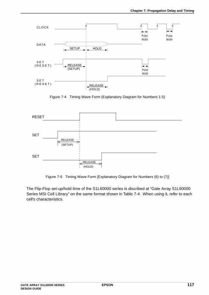
Chapter 7: Propagation Delay and Timing
Figure 7-4 Timing Wave Form (Explanatory Diagram for Numbers 1-5)
Figure 7-5 Timing Wave Form [Explanatory Diagram for Numbers (6) to (7)]
The Flip-Flop set-up/hold time of the S1L60000 series is discribed at “Gate Array S1L60000 Series MSI Cell Library” on the same format shown in Table 7-4. When using it, refer to each cell’s characteristics.
PulseWidth
CLOCK
DATA
RELEASE(SETUP)
S E T
SETUP HOLD
RELEASE(HOLD)
( R E S E T )
S E T( R E S E T )
PulseWidth
PulseWidth
RELEASE
(HOLD)
RELEASE
(SETUP)
SET
SET
RESET
GATE ARRAY S1L60000 SERIES EPSON 117DESIGN GUIDE
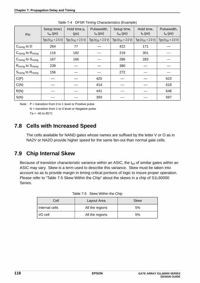
Chapter 7: Propagation Delay and Timing
Note : P = transition from 0 to 1 level or Positive pulse
N = transition from 1 to 0 level or Negative pulse
Ta = -40 to 85°C
7.8 Cells with Increased Speed
The cells available for NAND gates whose names are suffixed by the letter V or O as in NA2V or NA2O provide higher speed for the same fan-out than normal gate cells.
7.9 Chip Internal Skew
Because of transistor characteristic variance within an ASIC, the tpd of similar gates within an ASIC may vary. Skew is a term used to describe this variance. Skew must be taken into account so as to provide margin in timing critical portions of logic to insure proper operation.Please refer to “Table 7-5 Skew Within the Chip” about the skews in a chip of S1L60000 Series.
Table 7-4 DFSR Timing Characteristics (Example)
Pin
Setup time1tsu (ps)
Hold time,th(ps)
Pulsewidth,tw (ps)
Setup time,tsu (ps)
Hold time,th (ps)
Pulsewidth,tw (ps)
Typ.(VDD = 2.5 V) Typ.(VDD = 2.5 V) Typ.(VDD = 2.5 V) Typ.(VDD = 2.0 V) Typ.(VDD = 2.0 V) Typ.(VDD = 2.0 V)
Crising to D 264 77 — 422 171 —
Crising to Rrising 116 182 — 219 301 —
Crising to Srising 167 166 — 286 283 —
Rrising to Srising 239 — — 380 — —
Srising to Rrising 156 — — 272 — —
C(P) — — 425 — — 623
C(N) — — 414 — — 618
R(N) — — 441 — — 648
S(N) — — 393 — — 597
Table 7-5 Skew Within the Chip
Cell Layout Area Skew
Internal cells All the regions 5%
I/O cell All the regions 5%
118 EPSON GATE ARRAY S1L60000 SERIES DESIGN GUIDE
Chapter 8: Test Pattern Generation
Chapter 8 Test Pattern GenerationTest patterns must be generated once the logical design has been completed. Test patterns are used to simulate and verify circuit functionality. Test patterns are also used for product inspection prior to shipment. Please keep the following guidelines in mind when generating test patterns, thereby improving manufacturability and insuring product quality.
8.1 Testability Considerations
Because the test pattern is used in the final inspection of the product before it is shipped, it must be able to test all circuits within the LSI. If there are areas within the circuits of the LSI which are untested, it will not be possible to test those areas before the product is shipped, and thus there will be the danger of shipping defective product.
It is difficult to test all of the circuits within the LSI, so it is important to consider testability during the process of designing the circuit.
If the EPSON recommended test circuit is insert to the internal circuit of LSI, some conditions of DC test needed test patterns can be setting easily.
Refer to the section 6.3 about DC or AC test in detail.
8.2 Waveform Types
Although the test pattern is normally a series of “0” and “1” when a simulation is performed or the LSI tester are run, the input wave forms can be delayed, and the wave forms can be changed. The wave forms which can be used when the test pattern is generated include the following two types:
NRZ (Non Return to Zero)
A signal whose state changes no more than once per test period cycle is defined as being an NRZ type waveform. This waveform type can be delayed by a constant offset from the beginning of the test period cycle boundary.
RZ (Return to Zero)
A signal whose state may change twice per test period cycle is defined as being an RZ type waveform. This waveform type can be delayed by a constant offset from the beginning of the test period cycle boundary. This waveform type is useful for defining clock signals using positive or negative pulse definitions.
GATE ARRAY S1L60000 SERIES EPSON 119DESIGN GUIDE
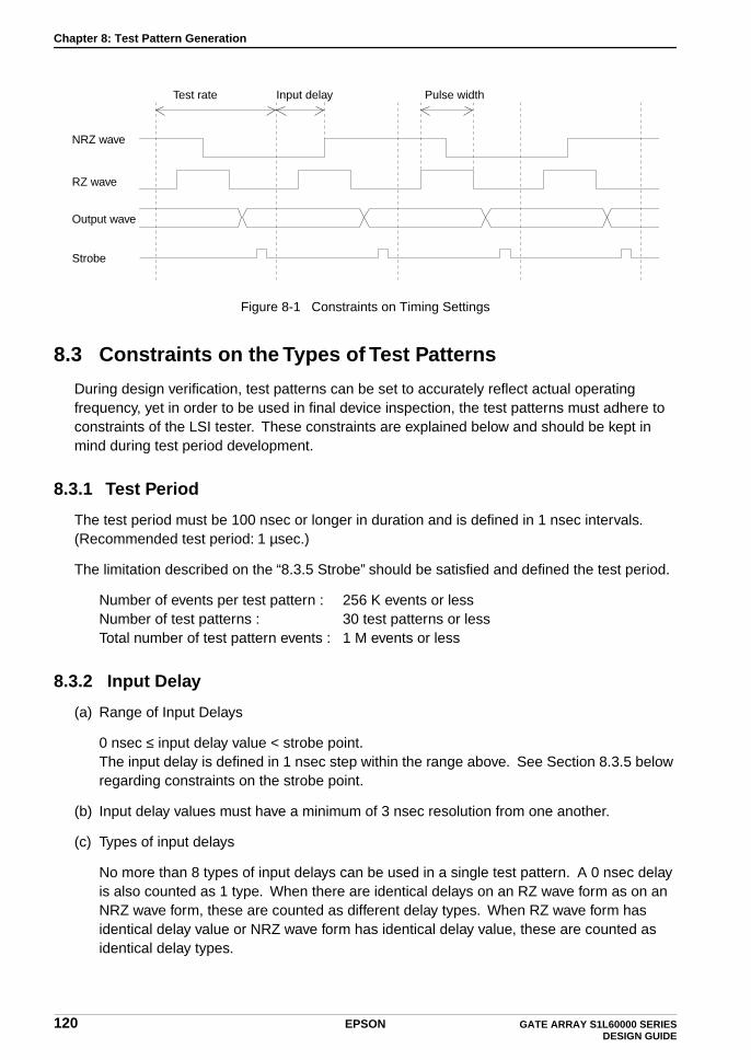
Chapter 8: Test Pattern Generation
Figure 8-1 Constraints on Timing Settings
8.3 Constraints on the Types of Test Patterns
During design verification, test patterns can be set to accurately reflect actual operating frequency, yet in order to be used in final device inspection, the test patterns must adhere to constraints of the LSI tester. These constraints are explained below and should be kept in mind during test period development.
8.3.1 Test Period
The test period must be 100 nsec or longer in duration and is defined in 1 nsec intervals. (Recommended test period: 1 µsec.)
The limitation described on the “8.3.5 Strobe” should be satisfied and defined the test period.
Number of events per test pattern : 256 K events or lessNumber of test patterns : 30 test patterns or lessTotal number of test pattern events : 1 M events or less
8.3.2 Input Delay
(a) Range of Input Delays
0 nsec ≤ input delay value < strobe point.The input delay is defined in 1 nsec step within the range above. See Section 8.3.5 below regarding constraints on the strobe point.
(b) Input delay values must have a minimum of 3 nsec resolution from one another.
(c) Types of input delays
No more than 8 types of input delays can be used in a single test pattern. A 0 nsec delay is also counted as 1 type. When there are identical delays on an RZ wave form as on an NRZ wave form, these are counted as different delay types. When RZ wave form has identical delay value or NRZ wave form has identical delay value, these are counted as identical delay types.
Test rate
RZ wave
Output wave
NRZ wave
Strobe
Input delay Pulse width
120 EPSON GATE ARRAY S1L60000 SERIES DESIGN GUIDE

Chapter 8: Test Pattern Generation
8.3.3 Pulse Width
Pulse widths for RZ wave forms must be 15 nsec or more.
8.3.4 Input Waveform Format
The input wave form must assume a value of “0”, “1”, “P”, or “N”. “P” and “N” indicate RZ positive pulse and negative pulse type. Use state “0” to disable positive pulse RZ waveform, and state “1” to disable negative pulse RZ waveform (i.e. RZ type state combinations of (0,P) and (1,N) are valid, while state combinations of (0,N) and (1,P) are invalid).
Do not use a bi-directional pin as the clock.
8.3.5 Strobe
The constraints on the strobe are as follows.
(a) Only a single strobe may be used within a single test pattern event.
(b) The smallest value for a strobe should be at least 30 nsec after the completion of all output signal changes, where the change results from input signals state change applied during that event.
(c) The maximum value for the strobe should be the test period minus 15 nsec.
(d) The strobe is defined in 1 nsec step.
8.4 Notes Regarding DC Testing
The test pattern is used for functional testing and DC testing of the LSI. Please generate the test patterns so that the following DC tests can be performed.
DC tests are performed to verify the DC parameters of the LSI. Because the DC tests perform measurements on the trailing edge of the measurement events, those terminals which are measured must not have state changes after the strobe during the measurement events.
The DC parameters measured are as described below:
(a) Output Driver Test (VOH, VOL)
The output buffer current driving capabilities are tested. The terminals which are to be tested are caused to enter the output level through the operation of the device, the specified current load is applied, and the level of the voltage drop is measured.
In order to perform the output driver tests, it is necessary for the test pattern to cause all of the terminals to enter all of the states which are obtained when the device is operating. Also, the states must be such that they do not change even if the measurement event extends the test period indefinitely.
GATE ARRAY S1L60000 SERIES EPSON 121DESIGN GUIDE
Chapter 8: Test Pattern Generation
(b) Quiescent Current Test (IDDS)
The quiescent current is the leakage current which flows to the LSI power supply when the input is in an fixed state. While generally this current is extremely small, this measurement must be done in a state where there are no other currents flowing aside from the leakage current. To do this, all of the following conditions must be fulfilled, and there must be two or more places wherein there are events which can measure the quiescent current.
(1) The input terminals are all in a fixed state.
(2) The bi-directional terminals are given High level or Low level inputs or are in an output state.
(3) There are no oscillators or operating functions within the circuit.
(4) None of the internal 3-state buffers (internal bus) are in a floating or a contention state.
(5) The RAM, the ROM, and the megacells are not in states wherein current is flowing.
(6) An High level input is applied to input terminals which have pull-up resistors.
(7) Bi-directional terminals with pull-up resistors attached are either given High level inputs or are producing High level outputs.
(8) Bi-directional terminals with pull-down resistors are either in an input state or are producing Low level outputs.
(c) The Input Current Test
The input current test measures the inputs to the input buffer. The test items include measurements of input leakage current and of pull-up/pull-down currents. The tests for these measurement items are performed by applying a VDD level or VSS level voltage to the terminal being measured, and measuring the current which flows. In other words, the test is performed by applying either an High level or a Low level voltage to the terminal being measured. For example, when a VDD (High level) signal is applied during the test to a terminal being measured and which is in a state having an Low level, then there is the potential for this to cause the state to change from Low to High in the terminal being measured, and the potential that this will cause the LSI to function incorrectly.
In order to measure the input current tests, a test where a VDD level is applied at an event where there is an High input to the terminal being measured in the test pattern, and a test is performed where a VSS level is applied in the event where a Low is applied. Because of this, it is not possible to perform these tests when the terminals being measured are not in these states in the test pattern.
122 EPSON GATE ARRAY S1L60000 SERIES DESIGN GUIDE
Chapter 8: Test Pattern Generation
The input current tests are further broken down into the following classifications.
(1) Input Leakage Current Test (IIH. IIL)
Measurements are performed regarding the input current of the input buffers which have no pull-up/pull-down resistors.
The current which flows when an High level voltage is applied to the input buffer is called IIH, and its maximum current value is guaranteed. In order to perform this test there must be an event in the test pattern which causes the input terminal to be measured to have an High level input. Bi-directional terminals must have High level inputs in the input state.
The current which flows when a Low level voltage is applied to the input buffer is called IIL, and its maximum value is guaranteed. In order to perform this test there must be an event in the test pattern which causes the input terminal to be measured to have a Low level input. Bi-directional terminals must have Low level inputs in the input state.
(2) Pull-up Current Tests (IPU)
This test measures the current which flows when an Low level voltage is applied to an input buffer having a pull-up resistor. In order to perform this test there must be an event in the test pattern which causes the input terminal to be measured to have an Low level input. Bi-directional terminals must have Low level inputs in the input state.
(3) Pull-down Current Tests (IPD)
This test measures the current which flows when an High level voltage is applied to an input buffer having a pull-down resistor. In order to perform this test there must be an event in the test pattern which causes the input terminal to be measured to have an High level input. Bi-directional terminals must have High level inputs in the input state.
(4) Off State Leakage Current (Ioz)
This measures the leakage current which flows when the output is a high-impedance state in output buffers which have open drains or which are 3-state output buffers. The actual measurement is the measurement of the currents when a VDD level voltage is applied, and when a VSS level voltage is applied to the terminal being measured when the terminal is in a high-impedance state. Because of this, the terminal being measured must enter into a high impedance state in the test pattern.
GATE ARRAY S1L60000 SERIES EPSON 123DESIGN GUIDE
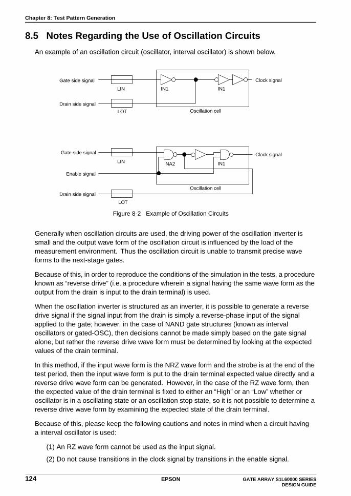
Chapter 8: Test Pattern Generation
8.5 Notes Regarding the Use of Oscillation Circuits
An example of an oscillation circuit (oscillator, interval oscillator) is shown below.
Figure 8-2 Example of Oscillation Circuits
Generally when oscillation circuits are used, the driving power of the oscillation inverter is small and the output wave form of the oscillation circuit is influenced by the load of the measurement environment. Thus the oscillation circuit is unable to transmit precise wave forms to the next-stage gates.
Because of this, in order to reproduce the conditions of the simulation in the tests, a procedure known as “reverse drive” (i.e. a procedure wherein a signal having the same wave form as the output from the drain is input to the drain terminal) is used.
When the oscillation inverter is structured as an inverter, it is possible to generate a reverse drive signal if the signal input from the drain is simply a reverse-phase input of the signal applied to the gate; however, in the case of NAND gate structures (known as interval oscillators or gated-OSC), then decisions cannot be made simply based on the gate signal alone, but rather the reverse drive wave form must be determined by looking at the expected values of the drain terminal.
In this method, if the input wave form is the NRZ wave form and the strobe is at the end of the test period, then the input wave form is put to the drain terminal expected value directly and a reverse drive wave form can be generated. However, in the case of the RZ wave form, then the expected value of the drain terminal is fixed to either an “High” or an “Low” whether or oscillator is in a oscillating state or an oscillation stop state, so it is not possible to determine a reverse drive wave form by examining the expected state of the drain terminal.
Because of this, please keep the following cautions and notes in mind when a circuit having a interval oscillator is used:
(1) An RZ wave form cannot be used as the input signal.
(2) Do not cause transitions in the clock signal by transitions in the enable signal.
Gate side signal
Drain side signal
LIN IN1 IN1
LOT
Enable signal
Clock signal
LIN NA2 IN1
Oscillation cell
LOT
Gate side signal
Drain side signalOscillation cell
Clock signal
124 EPSON GATE ARRAY S1L60000 SERIES DESIGN GUIDE
Chapter 8: Test Pattern Generation
8.6 Regarding AC Testing
AC testing measures the time it takes for a signal to propagate to the output terminal when there has been a transition at the input terminal during a single event. The AC testing can be performed on a measurement path selected by the customer.
8.6.1 Constraints Regarding Measurement Events
Because this test is done using a testing method known as the “normal binary search method,” the terminal being measured (i.e. the output terminal wherein there is a transition) must have only a single transition point within a measurement event. (Measurements cannot be performed on terminals having an RZ wave form output, nor can they be performed in situations where a hazard is output during the measurement event.) Also, the state transitions of the signal being measure must be either High to Low or Low to High. (Transitions involving a high-impedance state cannot be measured.)
Other cautions and notes include the necessity for selecting events so that there are no signal contentions between the bi-directional terminals and the LSI tester, and that there are no situations where many output terminals have simultaneous transitions at the measurement event. This is because the LSI power source is overwhelmed when there are simultaneous transitions or signal contentions, affecting the output wave form of the terminals being measured and making it impossible to get an accurate measurement.
8.6.2 Constraints on the Measurement Locations for AC Testing
Please use only 4 or less measurement locations in the AC testing.
8.6.3 Constraints Regarding the Path Delay Which is Tested
The longer the delay in the AC measurement, the more accurate the measurement. The measurement path delay time should be recorded using maximum delay simulation conditions targeting a path delay value of 30 nsec or more, and less than the strobe point.
8.6.4 Other Constraints
(1) Do not designate a path from the oscillator circuit.
(2) Designate a path which does not pass through a circuit having an internal 3-state unit (i.e. the internal bus).
(3) Do not designate a path passing through other bi-directional cells between the input cell and the output cell of the measurement path.
(4) When there are two or more voltage ranges used, reconcile these to a single AC test measurement voltages.
GATE ARRAY S1L60000 SERIES EPSON 125DESIGN GUIDE
Chapter 8: Test Pattern Generation
8.7 Test Pattern Constraints for Bi-directional Pins
By the constraints of testing, the bi-directional pins cannot switch between input mode and output mode more than once within a single event. Because of this, the test pattern generated should not use an RZ wave form for controlling the bi-directional cell input/output mode switching.
However you can use the RZ wave form for the bi-directional pins in the same way as for the input pins only when they are not under the output condition.
8.8 Notes on Devices at High Impedance
EPSON can not guarantee to operate the input pins of CMOS devices at high impedance, so EPSON forbids such operation when simulating the logic circuit. EPSON supplies the I/O cells with pull up or pull down resistor to prepare for high impedance. Furthermore, EPSON releases the pull up or pull down resistor of I/O cells so as not to consider the propagation delay time as mentioned. This is because accurate operation can not be simulated, so EPSON forbids the use of bi-directional pins with pull up or pull down resistor not to be inputted at the input mode when simulating the logic circuit.
<Reasons Why Propagation Delay Time of Pull up or Pull down Resistance is not Considered>
• Propagation is greatly changed by the capacity of the external load.
• The pull up or pull down resistor is only used to prevent to be floating gates at the high impedance.
EPSON checks the above using tools for the test patterns before simulating the logic circuit. If “Z” indicated to be high impedance is detected, the test patterns need to be changed.
In this case, “Z” detected at the bi-directional pins with a pull-up or pull-down resistor is also indicated to be in error for the reason noted above. Moreover, the same applies to the bi-directional pins of the open drain.
<Countermeasure>
When checking the test patterns, all of the “Z” values indicated to bi-directional pins are indicated to be in error. (Except for “Z” outputted at the output pins of 3-state and open drain)
EPSON supports the utility program for modifying the test patterns such that if “Z” is outputted at the bi-directional pin with pull up resistor, replace “1” and if “Z” is outputted at the bi-directional pin with pull down resistor, replace “0”.
If the bi-directional pin indicated by “X” is set to be the input mode, “X” is transferred at the simulation and the “?” is outputted as the simulation result. The “?” must be corrected, and then the simulation is executed again.
126 EPSON GATE ARRAY S1L60000 SERIES DESIGN GUIDE
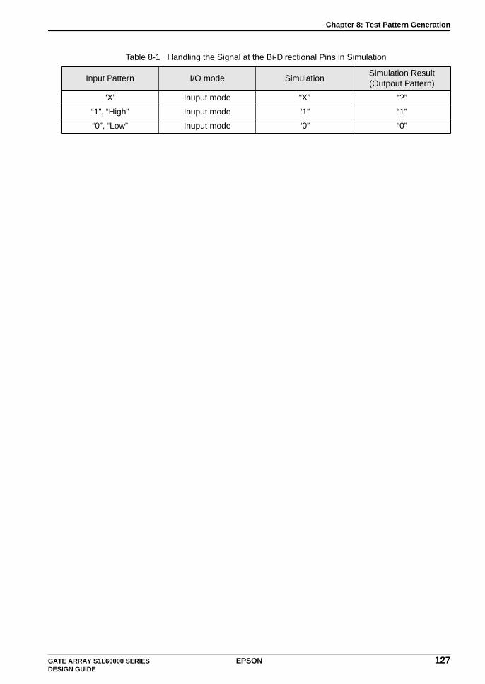
Chapter 8: Test Pattern Generation
Table 8-1 Handling the Signal at the Bi-Directional Pins in Simulation
Input Pattern I/O mode SimulationSimulation Result(Outpout Pattern)
“X” Inuput mode “X” “?”
“1”, “High” Inuput mode “1” “1”
“0”, “Low” Inuput mode “0” “0”
GATE ARRAY S1L60000 SERIES EPSON 127DESIGN GUIDE
Chapter 9: Estimating the Power Consumption
Chapter 9 Estimating the Power ConsumptionCMOS LSIs consume very little current when they are not operating. However, when they are operating, the power they consume depends on the operating frequency. When the power consumed is large, then the temperature of the LSI chip increases, and the quality of the LSI can be negatively affected if the temperature of the chip gets too high.
Because of this, it is necessary to calculate the power consumption and to check whether or not the power consumption is within allowable tolerances.
9.1 Calculating the Power Consumption
The power consumption of a CMOS circuit is generally dependent on the operating frequency, the capacitance, and the power supply voltage. (This excludes those special situations where there is a normal current through RAM/ROM, etc.) Here the CMOS gate array power consumption can be calculated easily if the operating frequencies and load captaincies of the various cells used within the circuit are known. However, because it is difficult to calculate the load captaincies for each internal cell, use the rough calculations described below.
After the power consumption for the input buffers, the output buffers and the internal cells are calculated, and these values are summed to produce the total power consumption.
Because of this, the total power consumption Ptotal is calculated as follows:
Pi : Power consumption of input bufferPtotal = Pi + PO + Pint Po : Power consumption of output buffer
Pint : Power consumption of internal cells
Please see Chapter 11 regarding power consumption calculations for dual power supplies.
(1) The Input buffer Power Consumption (Pi)
The input buffer power consumption is the sum of the products of the signal frequencies (MHz) input into each buffer, and the input buffer power coefficient Kp i (µW/MHz) for each buffer.
Kp i : Refer to Table 9-1 about the input buffer power coefficient (µW/MHz). Each value depends on the operating voltage.
f i : The operating frequency of the ith input buffer (MHz)
Table 9-1 Kp i of input buffer in the S1L60000 Series
VDD (Typ.) Kp i
2.5 V 2.6 µW/MHz
2.0 V 1.6 µW/MHz
Pi = ∑i=1
K (Kp i × f i) (W)
128 EPSON GATE ARRAY S1L60000 SERIES DESIGN GUIDE

Chapter 9: Estimating the Power Consumption
(2) Output Buffer Power Consumption (Po)
The output buffer power consumption differs depending on whether the load is a direct current load (such as resistive loads, TTL device connections, etc.) or whether the loads are alternating current loads (such as capacitance loads, CMOS device connections, etc.).
In the case of alternating current loads, the output buffer power consumption is calculated from the load capacitance CL as follows:
• Alternating current power consumption
PAC = f × CL × (VDD)2 (W)f: Output buffer operating frequency (Hz)CL: Load capacitance (F)VDD: Power supply voltage (V)
In the case of the direct current load, the power consumed in the direct current load is added to the power consumed in the alternating current load.
• Direct current power consumption
PDC = PDCH + PDCL
Where,PDCH = | IOH | × (VDD - VOH) (W)PDCL = IOL × VOL (W)
The ratio of PDCH and PDCL is determined by the output signal duty cycle.
Figure 9-1 Example of the Duty Cycle
Duty H = (T1 + T2) / TDuty L = (T - T1 - T2) / T
Because of this,
T
T1 T2
i=1
K = ∑ ( VDD-VOH i ) × IOH i × Duty H + ∑ VOL i × IOL i × Duty L
K
i=1
PDC = PDCH + PDCL
GATE ARRAY S1L60000 SERIES EPSON 129DESIGN GUIDE
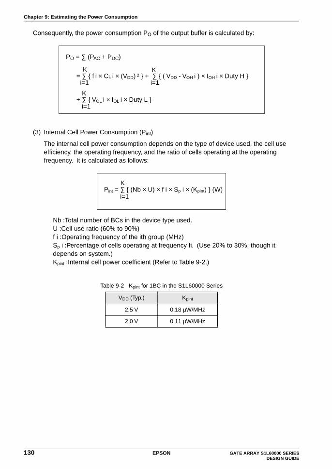
Chapter 9: Estimating the Power Consumption
Consequently, the power consumption PO of the output buffer is calculated by:
(3) Internal Cell Power Consumption (Pint)
The internal cell power consumption depends on the type of device used, the cell use efficiency, the operating frequency, and the ratio of cells operating at the operating frequency. It is calculated as follows:
Nb :Total number of BCs in the device type used.U :Cell use ratio (60% to 90%)f i :Operating frequency of the ith group (MHz)Sp i :Percentage of cells operating at frequency fi. (Use 20% to 30%, though it depends on system.)Kpint :Internal cell power coefficient (Refer to Table 9-2.)
Table 9-2 Kpint for 1BC in the S1L60000 Series
VDD (Typ.) Kpint
2.5 V 0.18 µW/MHz
2.0 V 0.11 µW/MHz
= ∑ f i × CL i × (VDD) 2 + ∑ ( VDD - VOH i ) × IOH i × Duty H K
i=1
+ ∑ VOL i × IOL i × Duty L K
i=1
PO = ∑ (PAC + PDC)
K
i=1
Pint = ∑ (Nb × U) × f i × Sp i × (Kpint) (W)K
i=1
130 EPSON GATE ARRAY S1L60000 SERIES DESIGN GUIDE

Chapter 9: Estimating the Power Consumption
9.2 Constraints on Power Consumption
The LSI chip heats up according to the power consumption within the LSI. The temperature of the LSI chip when it is mounted in a package can be calculated from the ambient temperature Ta, the thermal resistance(θj-a) of the package, and the power consumption PD.
The chip temperature (Tj) = Ta + (PD × θj-a) (°C)
In normal use, the chip temperature (Tj) should be less than about 125°C.
Please reference table 9-3 for the thermal resistances of each of the various packages. The thermal resistances listed in Table 9-3 will change substantially depending on the mounting of the packages on the circuit board and depending on whether or not there is forced air cooling.
Table 9-3 Thermal Resistances of Various Packages (Without Air Circulation)
QFP5QFP5QFP8QFP8QFP12QFP13QFP14QFP15
TQFP14TQFP14TQFP15
PIN
100128128208486480
100
80100100
110(°C/W)1106545230170110115
100100110
ALLOY42
θj-a θj-a θj-a
0 m/sec 1 m/sec 2 m/sec 3 m/sec
7575
————50
———
6060
————45
———
5555
—— — —
———35
QFP20 144 85 70 50 40———
QFP5QFP5QFP5QFP8QFP8QFP10QFP12QFP13QFP14QFP15QFP20QFP21QFP21QFP22QFP22QFP23QFP23TQFP12TQFP13TQFP15TQFP24HQFP5
H2QFP23H3QFP15
801001281602563044864801001841762162082561842404864128144128
240128
85(°C/W)808045503517513011090655555454540401651401058060
3085
Cu-L/F0 m/sec 1 m/sec 2 m/sec 3 m/sec
55555532—
2012080—————
3535———————
——
45353525—169055—————2525———————
——
40303023——8050—————2323———————
HQFP8 160 32 19 12 10
—H2QFP8 208 34 — — —
—
PBGAPBGAPBGA
225256388
72(°C/W)5345
PBGA0 m/sec 1 m/sec 2 m/sec 3 m/sec
4633—
3725—
———
θj-a θj-a θj-a θj-a θj-a
θj-a θj-a θj-a θj-a
PKG PINPKG
PINPKG
CFLGA424
CFLGA307
CFLGA239
CFLGA152
CFLGA104
75mm50mm30mm75mm50mm30mm75mm50mm30mm75mm50mm30mm75mm50mm30mm
CFLGA
3.82 mm ×3.82 mm
5.73 mm ×5.73 mm
Chip Size
44.0(°C/W)46.961.144.047.161.744.047.362.244.848.863.345.550.364.3
32.936.450.133.137.451.533.138.352.934.439.753.935.641.154.9
24.627.842.124.928.543.125.129.243.9
——————
9.55 mm ×9.55 mm
Customer’s board size
(Board installation under the windless condition)
Package type
GATE ARRAY S1L60000 SERIES EPSON 131DESIGN GUIDE

Chapter 10: Pin Layout Considerations
Chapter 10 Pin Layout Considerations
10.1 Estimating the Number of Power Supply Pins
It is necessary to estimate the number of power supply pins required based on the power consumed by the LSI and on the number of output buffers. The output buffers use a large current when switching. This current increases with larger output buffer drive capabilities.
The number of power supply pins required by the LSI can be estimated by its relationship with the current consumed as shown below.
If the current consumed is IDD (mA), then the number of power supply pins required (NIDD) to supply the consumption current IDD is as follows:
NIDD ≥ IDD /50 (pairs) : Possible to supply 50 mA for a pair of power supply
NOTE : Insert a minimum of 2 pairs of power pins NIDD.
IDD : Calculate IDD by dividing the power consumption calculated in Chapter 9 by the operating voltage.
See Chapter 11 regarding the estimation of the number of power pins for dual power supplies.
NOTE : When the DC load is connected to the output buffer, if the current is flowed at the steady-state, power supply pins should be added. For more infomation, contact to our sales office for technical support.
10.2 Number of Simultaneous Operations and Adding Power Supplies
In the S1L60000 Series, the output drive capability is extremely large at a maximum of 24 mA, and thus the noise generated by the output buffers when they are operating is also extremely large.
The power supplies need to be added, as shown in Table 10-1-1 to 10-2-2 to prevent malfunction from the noise when multiple output buffers operate at the same time.
132 EPSON GATE ARRAY S1L60000 SERIES DESIGN GUIDE

Chapter 10: Pin Layout Considerations
Table 10-1-1 Number of additional VSS Power Supplies Depending on theSimultaneous Operation of Output Buffers
(VDD = 2.5 V)
Output Drive Ability (IOL)
Number of Output Buffers Operating Simultaneously
Number of Additional Power Supplies
CL ≤ 50 pF CL ≤ 100 pF CL ≤ 200 pF
6 mA
≤8 0 1 2
≤16 1 2 3
≤24 1 2 4
≤32 2 3 5
9 mA
≤8 1 2 2
≤16 2 2 3
≤24 2 3 5
≤32 2 4 8
18 mA
≤8 2 3 4
≤16 3 4 6
≤24 4 6 8
≤32 6 8 16
PCI
≤8 1 2 3
≤16 2 3 4
≤24 3 4 5
≤32 4 5 10
Table 10-1-2 Number of additional VSS Power Supplies Depending on theSimultaneous Operation of Output Buffers
(VDD = 2.0 V)
Output Drive Ability (IOH)
Number of Output Buffers Operating Simultaneously
Number of Additional Power Supplies
CL ≤ 50 pF CL ≤ 100 pF CL ≤ 200 pF
3 mA
≤8 0 1 2
≤16 1 2 3
≤24 1 2 4
≤32 2 3 5
6 mA
≤8 0 1 2
≤16 1 2 4
≤24 1 3 6
≤32 2 4 8
GATE ARRAY S1L60000 SERIES EPSON 133DESIGN GUIDE
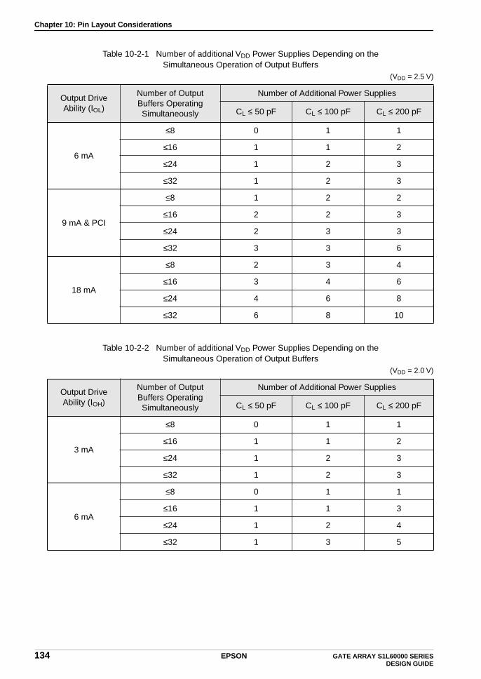
Chapter 10: Pin Layout Considerations
Table 10-2-1 Number of additional VDD Power Supplies Depending on theSimultaneous Operation of Output Buffers
(VDD = 2.5 V)
Output Drive Ability (IOL)
Number of Output Buffers Operating Simultaneously
Number of Additional Power Supplies
CL ≤ 50 pF CL ≤ 100 pF CL ≤ 200 pF
6 mA
≤8 0 1 1
≤16 1 1 2
≤24 1 2 3
≤32 1 2 3
9 mA & PCI
≤8 1 2 2
≤16 2 2 3
≤24 2 3 3
≤32 3 3 6
18 mA
≤8 2 3 4
≤16 3 4 6
≤24 4 6 8
≤32 6 8 10
Table 10-2-2 Number of additional VDD Power Supplies Depending on theSimultaneous Operation of Output Buffers
(VDD = 2.0 V)
Output Drive Ability (IOH)
Number of Output Buffers Operating Simultaneously
Number of Additional Power Supplies
CL ≤ 50 pF CL ≤ 100 pF CL ≤ 200 pF
3 mA
≤8 0 1 1
≤16 1 1 2
≤24 1 2 3
≤32 1 2 3
6 mA
≤8 0 1 1
≤16 1 1 3
≤24 1 2 4
≤32 1 3 5
134 EPSON GATE ARRAY S1L60000 SERIES DESIGN GUIDE

Chapter 10: Pin Layout Considerations
10.3 Cautions and Notes Regarding the Layout of pins
Once the package to be used has been selected, then it is time to layout the pins. Please see the specific “Pin Layout Table” regarding the number of power supply pins and useable input/output pins in the various S1L60000 Series Packages.
Once the pin layout has been established, submit to EPSON a pin assignment specificationwhich has been filled out with the pin layout. EPSON will layout the interconnections according to the specification submitted by the customer, so we request that the customer carefully check this specification.
Please request the specific “Pin Layout Table” from our sales staff.
The pin layout is one of the critical specifications which controls the quality of the LSI. It is especially important in avoiding malfunctions due to noise. Moreover, problems with noise are difficult to check for in simulations. So that there will be are no malfunctions with non-traceable causes in the customer’s LSI, we urge the customer to carefully study the guidelines detailed in this chapter before generating the pin layout.
10.3.1 Fixed Power Supply Pins
There are some pins which can only be used for power supply, depending on the combination of each device and package in this series. Because there are some pins which must be set to VDD pins and some pins which must be set to VSS pins please consult with EPSON when selecting a package.
10.3.2 Cautions and Notes Regarding the Pin Layout
The pin layout influences the logical functioning and electrical characteristics of the LSI. Moreover, the pin layout may be constrained by the construction of the LSI, the structuring of the cells and the bulk, etc. Because of this, we will explain factors which must be researched when creating the pin layout, factors such as the power supply current, the input pin/output pin isolation, the critical signals, the pull-up/pull-down resistor inputs, simultaneous output, current drivers, etc.
(1) Power Supply Currenµt (IDD, ISS)
When it comes to the power supply current (IDD, ISS) there are limitations on the tolerable levels for current from the power supply through the power supply pins when in an operating state. When the tolerable levels are exceeded, the current density within the power supply interconnects within the LSI becomes too high, and the voltage generated by the current and the resistance within the interconnects increases or decreases. This may lead to malfunctioning and may have an impact on DC or AC characteristics.
In order to avoid these types of problems, it is necessary to reduce the current density and the power supply interconnect line impedance. To do this, it is necessary to estimate the power consumption during the design of the gate array, and to make sure that there are enough power supply pins so that the current through each of the power supply pins does not exceed tolerances. Moreover, the layout should be such that the power supply pins are not concentrated all in one location, but rather are spread out. See Section 10.1, “Estimating the Number of Power Supply Pins” about number of power supply pins.
GATE ARRAY S1L60000 SERIES EPSON 135DESIGN GUIDE
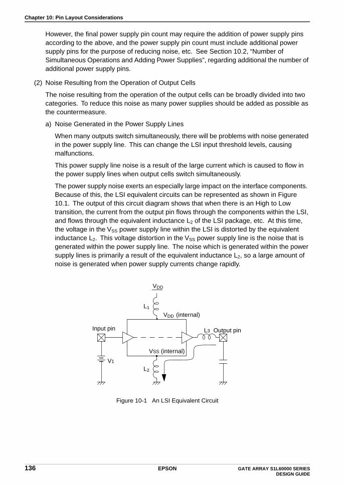
Chapter 10: Pin Layout Considerations
However, the final power supply pin count may require the addition of power supply pins according to the above, and the power supply pin count must include additional power supply pins for the purpose of reducing noise, etc. See Section 10.2, “Number of Simultaneous Operations and Adding Power Supplies”, regarding additional the number of additional power supply pins.
(2) Noise Resulting from the Operation of Output Cells
The noise resulting from the operation of the output cells can be broadly divided into two categories. To reduce this noise as many power supplies should be added as possible as the countermeasure.
a) Noise Generated in the Power Supply Lines
When many outputs switch simultaneously, there will be problems with noise generated in the power supply line. This can change the LSI input threshold levels, causing malfunctions.
This power supply line noise is a result of the large current which is caused to flow in the power supply lines when output cells switch simultaneously.
The power supply noise exerts an especially large impact on the interface components. Because of this, the LSI equivalent circuits can be represented as shown in Figure 10.1. The output of this circuit diagram shows that when there is an High to Low transition, the current from the output pin flows through the components within the LSI, and flows through the equivalent inductance L2 of the LSI package, etc. At this time, the voltage in the VSS power supply line within the LSI is distorted by the equivalent inductance L2. This voltage distortion in the VSS power supply line is the noise that is generated within the power supply line. The noise which is generated within the power supply lines is primarily a result of the equivalent inductance L2, so a large amount of noise is generated when power supply currents change rapidly.
Figure 10-1 An LSI Equivalent Circuit
VDD
Input pin
VDD (internal)
VSS (internal)
L1
L2
L3
V1
Output pin
136 EPSON GATE ARRAY S1L60000 SERIES DESIGN GUIDE
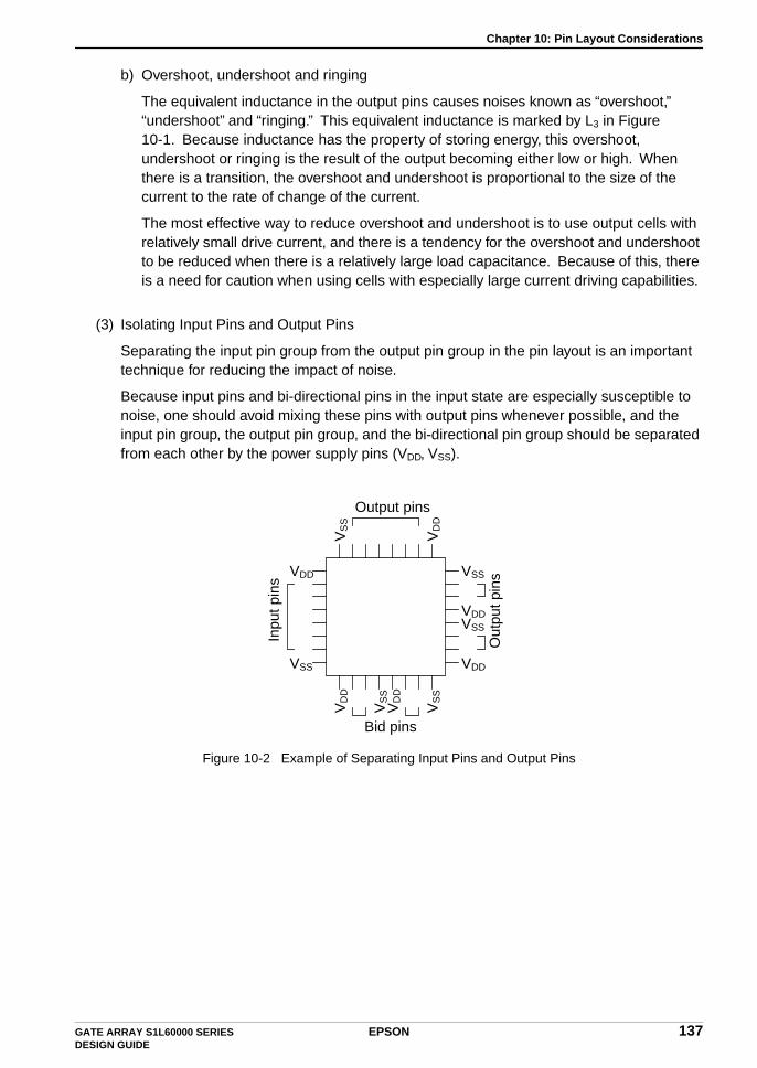
Chapter 10: Pin Layout Considerations
b) Overshoot, undershoot and ringing
The equivalent inductance in the output pins causes noises known as “overshoot,” “undershoot” and “ringing.” This equivalent inductance is marked by L3 in Figure 10-1. Because inductance has the property of storing energy, this overshoot, undershoot or ringing is the result of the output becoming either low or high. When there is a transition, the overshoot and undershoot is proportional to the size of the current to the rate of change of the current.
The most effective way to reduce overshoot and undershoot is to use output cells with relatively small drive current, and there is a tendency for the overshoot and undershoot to be reduced when there is a relatively large load capacitance. Because of this, there is a need for caution when using cells with especially large current driving capabilities.
(3) Isolating Input Pins and Output Pins
Separating the input pin group from the output pin group in the pin layout is an important technique for reducing the impact of noise.
Because input pins and bi-directional pins in the input state are especially susceptible to noise, one should avoid mixing these pins with output pins whenever possible, and the input pin group, the output pin group, and the bi-directional pin group should be separated from each other by the power supply pins (VDD, VSS).
Figure 10-2 Example of Separating Input Pins and Output Pins
VDD
VSS
VD
D
VD
D
VDD
VDD
VD
D
VSS
VSS
VS
S
VS
S
VS
S
Output pinsO
utpu
t pin
s
Inpu
t pin
s
Bid pins
GATE ARRAY S1L60000 SERIES EPSON 137DESIGN GUIDE

Chapter 10: Pin Layout Considerations
(4) Critical Signals
The following cautions and notes should be kept in mind when laying out the pins for critical signals such as clock input pins and high-speed output pins.
a) Pins for which it is necessary to reduce the noise, such as clock and reset pins, should be placed near the power supply pins and far from the output pins. (See Figure 10-3)
b) Oscillator circuit pins should be placed near one another, sandwiched between power supply pins (VDD, VSS). Moreover, they should not be placed near output pins. (See Figure 10-4.)
c) High-speed input and output pins should be placed near the center of the edge of the chip (of the package). (See Figure 10-3.)
d) When there is little margin in the customer specifications for delays between the input pins and the output pins, these input and output pins should be placed near to one another. (See Figure 10-3.)
Figure 10-3 Example 1 of a Layout for Critical Signals
Figure 10-4 Example 2 of a Layout for Critical Signals
RS
TC
LKV
SS
VS
S
High speed inputThrough input
Through output
High speed output
VSS
OSCIN
VDD
VSS
OSCOUT
138 EPSON GATE ARRAY S1L60000 SERIES DESIGN GUIDE

Chapter 10: Pin Layout Considerations
(5) Pull-up/Pull-down Resistor Inputs
The pull-up and pull-down resistance values are relatively large, ranging from a few dozen to a few hundred kohms. The structure of the resistors depends on the power supply voltage. Because of this, the pins are especially vulnerable to noise coming from the power supply. The following cautions should be carefully considered when creating the pin layout in order to prevent this noise from causing malfunctions.
a) Locate as far as possible from high-speed inputs (such as clock pins). (See Figure 10-5.)
b) Locate away from output pins (especially large-current output pins). (See Figure 10-6.)
Please consider the following points prior to pin layout.
• Perform pull-up and pull-down processes on the PCB itself whenever possible.
• Select resistors with low resistances whenever possible.
Figure 10-5 Example 1 of Placement of Pull-up and Pull-down Resistors
Figure 10-6 Example 2 of Placement of Pull-up and Pull-down Resistors
CLK PULL UP
PULL DOWN High drive output
GATE ARRAY S1L60000 SERIES EPSON 139DESIGN GUIDE
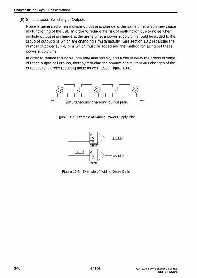
Chapter 10: Pin Layout Considerations
(6) Simultaneous Switching of Outputs
Noise is generated when multiple output pins change at the same time, which may cause malfunctioning of the LSI. In order to reduce the risk of malfunction due to noise when multiple output pins change at the same time, a power supply pin should be added to the group of output pins which are changing simultaneously. See section 10.2 regarding the number of power supply pins which must be added and the method for laying out these power supply pins.
In order to reduce this noise, one may alternatively add a cell to delay the previous stage of these output cell groups, thereby reducing the amount of simultaneous changes of the output cells, thereby reducing noise as well. (See Figure 10-8.)
Figure 10-7 Example of Adding Power Supply Pins
Figure 10-8 Example of Adding Delay Cells
VD
DV
SS
VD
DV
SS
VD
D
VS
S
VS
S
VS
S
Simultaneously changing output pins.
AOUT1
OB3T
AOUT2
OB3T
TATS
TATS
DL1
140 EPSON GATE ARRAY S1L60000 SERIES DESIGN GUIDE
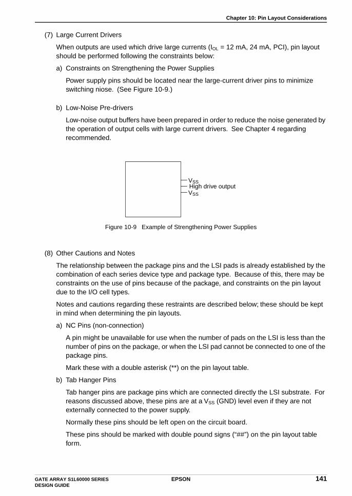
Chapter 10: Pin Layout Considerations
(7) Large Current Drivers
When outputs are used which drive large currents (IOL = 12 mA, 24 mA, PCI), pin layout should be performed following the constraints below:
a) Constraints on Strengthening the Power Supplies
Power supply pins should be located near the large-current driver pins to minimize switching niose. (See Figure 10-9.)
b) Low-Noise Pre-drivers
Low-noise output buffers have been prepared in order to reduce the noise generated by the operation of output cells with large current drivers. See Chapter 4 regarding recommended.
Figure 10-9 Example of Strengthening Power Supplies
(8) Other Cautions and Notes
The relationship between the package pins and the LSI pads is already established by the combination of each series device type and package type. Because of this, there may be constraints on the use of pins because of the package, and constraints on the pin layout due to the I/O cell types.
Notes and cautions regarding these restraints are described below; these should be kept in mind when determining the pin layouts.
a) NC Pins (non-connection)
A pin might be unavailable for use when the number of pads on the LSI is less than the number of pins on the package, or when the LSI pad cannot be connected to one of the package pins.
Mark these with a double asterisk (**) on the pin layout table.
b) Tab Hanger Pins
Tab hanger pins are package pins which are connected directly the LSI substrate. For reasons discussed above, these pins are at a VSS (GND) level even if they are not externally connected to the power supply.
Normally these pins should be left open on the circuit board.
These pins should be marked with double pound signs (“##”) on the pin layout table form.
VSS
VSS
High drive output
GATE ARRAY S1L60000 SERIES EPSON 141DESIGN GUIDE
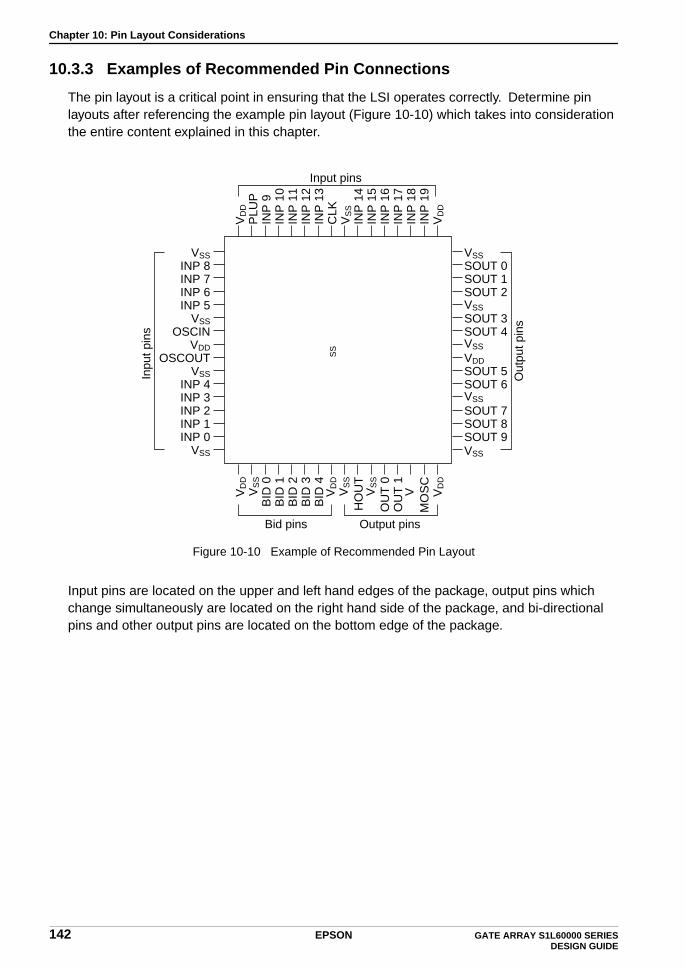
Chapter 10: Pin Layout Considerations
10.3.3 Examples of Recommended Pin Connections
The pin layout is a critical point in ensuring that the LSI operates correctly. Determine pin layouts after referencing the example pin layout (Figure 10-10) which takes into consideration the entire content explained in this chapter.
Figure 10-10 Example of Recommended Pin Layout
Input pins are located on the upper and left hand edges of the package, output pins which change simultaneously are located on the right hand side of the package, and bi-directional pins and other output pins are located on the bottom edge of the package.
VD
DP
LUP
INP
9IN
P10
INP
11IN
P12
INP
13C
LKV
SS
INP
14IN
P15
INP
16IN
P17
INP
18IN
P19
VD
D
VSSSOUT 0SOUT 1SOUT 2
SOUT 3SOUT 4
VDDSOUT 5SOUT 6
SOUT 7SOUT 8SOUT 9
VSSINP 8INP 7INP 6INP 5
VSSOSCIN
VDDOSCOUT
VSSINP 4INP 3INP 2INP 1INP 0
VSS
VD
DV
SS
BID
0B
ID1
BID
2B
ID3
BID
4
HO
UT
OU
T0
OU
T1
MO
SC
VD
D
Input pins
Out
putp
ins
Inpu
tpin
s
Bid pins Output pins
VD
DV
SS
VS
S
V
SS
VSS
VSS
VSS
VSS
142 EPSON GATE ARRAY S1L60000 SERIES DESIGN GUIDE
Chapter 10: Pin Layout Considerations
Table 10-3 Pin Layout Example
Location Pin NameExplanation of Pin
NameDetailed Explanation of the Position of Each Pin
Upper Edge PULPCLK
Input pins with pull-upsInput pins for the clock
Located where the impact of noise is the least. Located near the center of the package, and near power supply pins.
Left Edge OSCIN, OSCOUTINP0 to19
Oscillator pins
Input pins
Located near the center of the package, and near power supply pins.Located with power supply pins, away from other pins.
Right-hand Edge
SOUT0 to 9 Simultaneously changing output pins
Located near power supply pins and separated from other pins with additional power supply pins.
Bottom Edge BID0 to 4
MOSC
HOUTOUT01
Bi-directional pins
Oscillator monitor output pinsHigh-drive output pins Output pins
Located near power supply pins and separated from other pins.Located separated from oscillator pins and near power supply pins.Located near power supply pins.Located near power supply pins and separated from other pins.
All Edges VDD
VSS
VDD power supply pinsVSS (GND) power supply pins
GATE ARRAY S1L60000 SERIES EPSON 143DESIGN GUIDE

Chapter 11: Dual Power Supplies Guidelines
Chapter 11 Dual Power Supplies GuidelinesBy using dual power supplies (3.3 V/2.5 V or 3.3 V/2.0 V systems) the S1L60000 Series is able to interface with either 3.3 V, 2.5 V or 2.0 V system signal for each I/O cell. The internal cell region operates on only the single 2.5 V or 2.0 V system power supply.
11.1 The Method of Adapting to Dual Power Supplies
The S1L60000 Series is of capable of interfacing with signals of a voltage which is different than the internal operating voltage. There are two methods by which to interface with systems of different voltages.
• The Single Power Supply Method
With a single power supply, it is possible to input signals with operating voltages that are higher than the supply voltage, by using an Nch open-drain buffer or a fail-safe cell. However, it is not possible to output signals with operating voltages that are higher than the supply voltage, unless an Nch open-drain buffer and an external pull-up resistor are combined.
• The Dual Power Supply Method
It is possible to input a signal of a higher voltage than the internal operating voltage through the use of special dual power supply compatible input butters. Also, the use of output buffers with level shifters makes it possible to output signals of voltages higher than internal operating voltage.
11.2 Power Supplies for Dual Power Operation
When two power supplies are applied, use the unique power supply identifiers, HVDD and LVDD. HVDD is used to supply power for HVDD’ I/O cells. LVDD is used to supply power for LVDD’ I/O cells and all internal cells. The power supply voltages must always fulfill the following inequality:
HVDD ≥ LVDD
Caution is necessary because operation cannot be assured if HVDD is less than LVDD. The following two conditions are recommended operating conditions.
• HVDD = 3.3 V, LVDD = 2.5 V
• HVDD = 3.3 V, LVDD = 2.0 V
144 EPSON GATE ARRAY S1L60000 SERIES DESIGN GUIDE
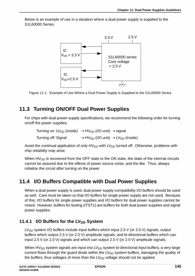
Chapter 11: Dual Power Supplies Guidelines
Below is an example of use in a situation where a dual power supply is supplied to the S1L60000 Series.
Figure 11-1 Example of Use Where a Dual Power Supply is Supplied to the S1L60000 Series
11.3 Turming ON/OFF Dual Power Supplies
For chips with dual-power-supply specifications, we recommend the following order for turning on/off the power supplies.
Turning on: LVDD (inside) HVDD (I/O unit) signal
Turning off: Signal HVDD (I/O unit) LVDD (inside)
Avoid the continual application of only HVDD with LVDD turned off. Otherwise, problems with chip reliability may arise.
When HVDD is recovered from the OFF state to the ON state, the state of the internal circuits cannot be assured due to the effects of power source noise, and the like. Thus, always initialize the circuit after turning on the power.
11.4 I/O Buffers Compatible with Dual Power Supplies
When a dual power supply is used, dual power supply-compatibility I/O buffers should be used as well. Care must be taken so that I/O buffers for single power supply are not used. Because of this, I/O buffers for single power supplies and I/O buffers for dual power supplies cannot be mixed. However, buffers for testing (ITST1) are buffers for both dual power supplies and signal power supplies.
11.4.1 I/O Buffers for the LVDD System
LVDD system I/O buffers include input buffers which input 2.5 V (or 2.0 V) signals, output buffers which output 2.5 V (or 2.0 V) amplitude signals, and bi-directional buffers which can input 2.5 V (or 2.0 V) signals and which can output 2.5 V (or 2.0 V) amplitude signals.
When HVDD system signals are input into LVDD system bi-directional input buffers, a very large current flows through the guard diode within the LVDD system buffers, damaging the quality of the buffers; thus voltages of more than the LVDD voltage should not be applied.
S1L60000 seriesCore voltage = 2.5 V
3.3 V 2.5 V
ICVDD = 3.3 V
ICVDD=2.5 V
GATE ARRAY S1L60000 SERIES EPSON 145DESIGN GUIDE

Chapter 11: Dual Power Supplies Guidelines
11.4.1.1 Input Buffers for the LVDD System
The input buffer is comprised of only input cells. The LVDD system input signals include those shown in Table 11-1-1 and Table 11-1-2.
NOTE: When ∗ value is 1 or 2, the pull-up/pull-down resistance values correspond to 1: 50 kΩ, 2:100 kΩ respectively.
NOTE: When ∗ value is 1 or 2, the pull-up/pull-down resistance values correspond to 1: 70 kΩ, 2:140 kΩ respectively.
Table 11-1-1 LVDD System Input Buffers(LVDD = 2.5 V)
Cell Name Input Level Function Pull-up/Pull-down Resistors
LIBCLIBCP∗LIBCD∗
CMOSCMOSCMOS
BufferBufferBuffer
NonePull-up Resistor (50 kΩ, 100 kΩ)
Pull-down Resistor (50 kΩ, 100 kΩ)
LIBHLIBHP∗LIBHD∗
CMOS SchmittCMOS SchmittCMOS Schmitt
BufferBufferBuffer
NonePull-up Resistor (50 kΩ, 100 kΩ)
Pull-down Resistor (50 kΩ, 100 kΩ)
Table 11-1-2 LVDD System Input Buffers(LVDD = 2.0 V)
Cell Name Input Level Function Pull-up/Pull-down Resistors
LIBCLIBCP∗LIBCD∗
CMOSCMOSCMOS
BufferBufferBuffer
NonePull-up Resistor (70 kΩ, 140 kΩ)
Pull-down Resistor (70 kΩ, 140 kΩ)
LIBHLIBHP∗LIBHD∗
CMOS SchmittCMOS SchmittCMOS Schmitt
BufferBufferBuffer
NonePull-up Resistor (70 kΩ, 140 kΩ)
Pull-down Resistor (70 kΩ, 140 kΩ)
146 EPSON GATE ARRAY S1L60000 SERIES DESIGN GUIDE
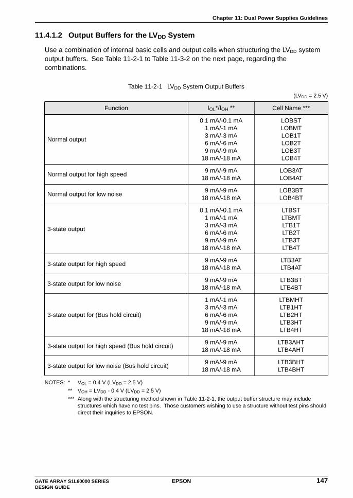
Chapter 11: Dual Power Supplies Guidelines
11.4.1.2 Output Buffers for the LVDD System
Use a combination of internal basic cells and output cells when structuring the LVDD system output buffers. See Table 11-2-1 to Table 11-3-2 on the next page, regarding the combinations.
NOTES: * VOL = 0.4 V (LVDD = 2.5 V)
** VOH = LVDD - 0.4 V (LVDD = 2.5 V)
*** Along with the structuring method shown in Table 11-2-1, the output buffer structure may include structures which have no test pins. Those customers wishing to use a structure without test pins should direct their inquiries to EPSON.
Table 11-2-1 LVDD System Output Buffers(LVDD = 2.5 V)
Function IOL*/IOH ** Cell Name ***
Normal output
0.1 mA/-0.1 mA1 mA/-1 mA3 mA/-3 mA6 mA/-6 mA9 mA/-9 mA
18 mA/-18 mA
LOBSTLOBMTLOB1TLOB2TLOB3TLOB4T
Normal output for high speed 9 mA/-9 mA
18 mA/-18 mALOB3ATLOB4AT
Normal output for low noise 9 mA/-9 mA
18 mA/-18 mALOB3BTLOB4BT
3-state output
0.1 mA/-0.1 mA1 mA/-1 mA3 mA/-3 mA6 mA/-6 mA9 mA/-9 mA
18 mA/-18 mA
LTBSTLTBMTLTB1TLTB2TLTB3TLTB4T
3-state output for high speed 9 mA/-9 mA
18 mA/-18 mALTB3ATLTB4AT
3-state output for low noise9 mA/-9 mA
18 mA/-18 mALTB3BTLTB4BT
3-state output for (Bus hold circuit)
1 mA/-1 mA3 mA/-3 mA6 mA/-6 mA9 mA/-9 mA
18 mA/-18 mA
LTBMHTLTB1HTLTB2HTLTB3HTLTB4HT
3-state output for high speed (Bus hold circuit)9 mA/-9 mA
18 mA/-18 mALTB3AHTLTB4AHT
3-state output for low noise (Bus hold circuit)9 mA/-9 mA
18 mA/-18 mALTB3BHTLTB4BHT
GATE ARRAY S1L60000 SERIES EPSON 147DESIGN GUIDE

Chapter 11: Dual Power Supplies Guidelines
NOTES: * VOL = 0.2 V (LVDD = 2.0 V)
** VOH = LVDD - 0.2 V (LVDD = 2.0 V)
*** Along with the structuring method shown in Table 11-2-2, the output buffer structure may include structures which have no test pins. Those customers wishing to use a structure without test pins should direct their inquiries to EPSON.
Table 11-2-2 LVDD System Output Buffers(LVDD = 2.0 V)
Function IOL*/IOH ** Cell Name ***
Normal output
0.05 mA/-0.05 mA0.3 mA/-0.3 mA
1 mA/-1 mA2 mA/-2 mA3 mA/-3 mA6 mA/-6 mA
LOBSTLOBMTLOB1TLOB2TLOB3TLOB4T
Normal output for high speed 3 mA/-3 mA6 mA/-6 mA
LOB3ATLOB4AT
Normal output for low noise 3 mA/-3 mA6 mA/-6 mA
LOB3BTLOB4BT
3-state output
0.05 mA/-0.05 mA0.3 mA/-0.3 mA
1 mA/-1 mA2 mA/-2 mA3 mA/-3 mA6 mA/-6 mA
LTBSTLTBMTLTB1TLTB2TLTB3TLTB4T
3-state output for high speed 3 mA/-3 mA6 mA/-6 mA
LTB3ATLTB4AT
3-state output for low noise3 mA/-3 mA6 mA/-6 mA
LTB3BTLTB4BT
3-state output for (Bus hold circuit)
0.3 mA/-0.3 mA1 mA/-1 mA2 mA/-2 mA3 mA/-3 mA6 mA/-6 mA
LTBMHTLTB1HTLTB2HTLTB3HTLTB4HT
3-state output for high speed (Bus hold circuit)3 mA/-3 mA6 mA/-6 mA
LTB3AHTLTB4AHT
3-state output for low noise (Bus hold circuit)3 mA/-3 mA6 mA/-6 mA
LTB3BHTLTB4BHT
148 EPSON GATE ARRAY S1L60000 SERIES DESIGN GUIDE
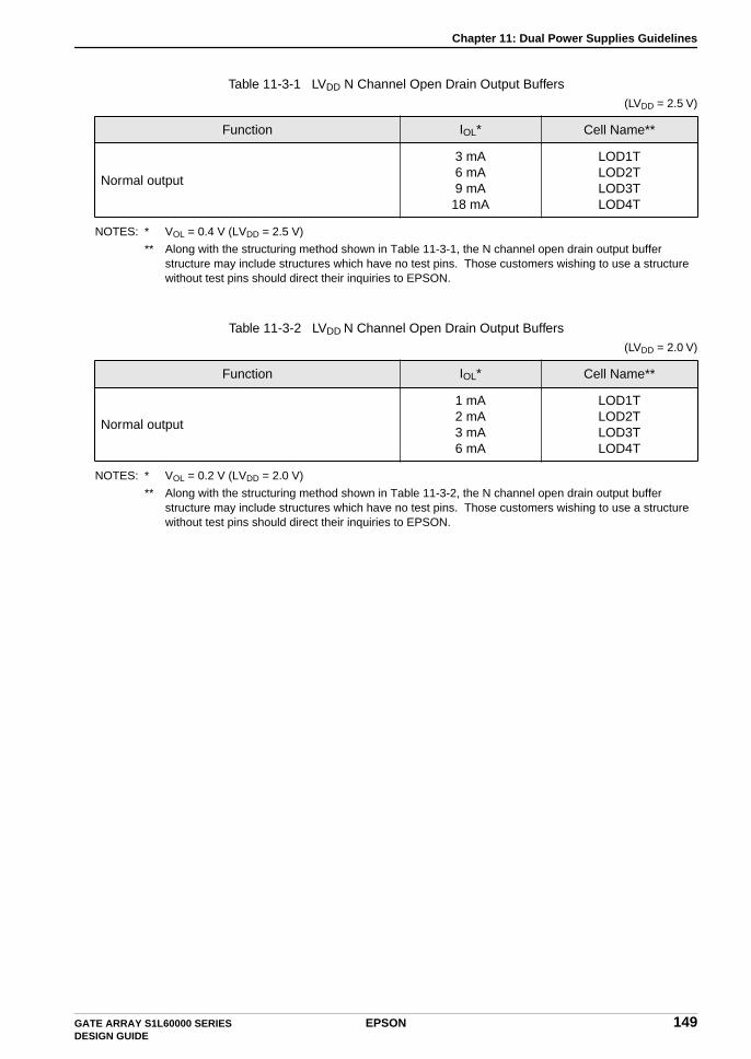
Chapter 11: Dual Power Supplies Guidelines
NOTES: * VOL = 0.4 V (LVDD = 2.5 V)
** Along with the structuring method shown in Table 11-3-1, the N channel open drain output buffer structure may include structures which have no test pins. Those customers wishing to use a structure without test pins should direct their inquiries to EPSON.
NOTES: * VOL = 0.2 V (LVDD = 2.0 V)
** Along with the structuring method shown in Table 11-3-2, the N channel open drain output buffer structure may include structures which have no test pins. Those customers wishing to use a structure without test pins should direct their inquiries to EPSON.
Table 11-3-1 LVDD N Channel Open Drain Output Buffers(LVDD = 2.5 V)
Function IOL* Cell Name**
Normal output
3 mA6 mA9 mA18 mA
LOD1TLOD2TLOD3TLOD4T
Table 11-3-2 LVDD N Channel Open Drain Output Buffers(LVDD = 2.0 V)
Function IOL* Cell Name**
Normal output
1 mA2 mA3 mA6 mA
LOD1TLOD2TLOD3TLOD4T
GATE ARRAY S1L60000 SERIES EPSON 149DESIGN GUIDE
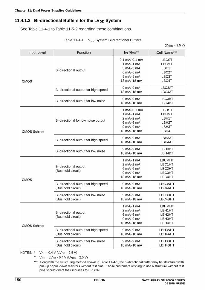
Chapter 11: Dual Power Supplies Guidelines
11.4.1.3 Bi-directional Buffers for the LVDD System
See Table 11-4-1 to Table 11-5-2 regarding these combinations.
NOTES: * VOL = 0.4 V (LVDD = 2.5 V)
** VOH = LVDD - 0.4 V (LVDD = 2.5 V)
*** Along with the structuring method shown in Table 11-4-1, the bi-directional buffer may be structured with pull-up or pull-down resistors without test pins. Those customers wishing to use a structure without test pins should direct their inquiries to EPSON.
Table 11-4-1 LVDD System Bi-directional Buffers(LVDD = 2.5 V)
Input Level Function IOL*/IOH** Cell Name***
CMOS
Bi-directional output
0.1 mA/-0.1 mA1 mA/-1 mA3 mA/-3 mA6 mA/-6 mA9 mA/-9 mA
18 mA/-18 mA
LBCSTLBCMTLBC1TLBC2TLBC3TLBC4T
Bi-directional output for high speed9 mA/-9 mA
18 mA/-18 mALBC3ATLBC4AT
Bi-directional output for low noise9 mA/-9 mA
18 mA/-18 mALBC3BTLBC4BT
CMOS Schmitt
Bi-directional for low noise output
0.1 mA/-0.1 mA1 mA/-1 mA2 mA/-2 mA6 mA/-6 mA9 mA/-9 mA
18 mA/-18 mA
LBHSTLBHMTLBH1TLBH2TLBH3TLBH4T
Bi-directional output for high speed9 mA/-9 mA
18 mA/-18 mALBH3ATLBH4AT
Bi-directional output for low noise9 mA/-9 mA
18 mA/-18 mALBH3BTLBH4BT
CMOS
Bi-directional output (Bus hold circuit)
1 mA/-1 mA2 mA/-2 mA6 mA/-6 mA9 mA/-9 mA
18 mA/-18 mA
LBCMHTLBC1HTLBC2HTLBC3HTLBC4HT
Bi-directional output for high speed(Bus hold circuit)
9 mA/-9 mA18 mA/-18 mA
LBC3AHTLBC4AHT
Bi-directional output for low noise(Bus hold circuit)
9 mA/-9 mA18 mA/-18 mA
LBC3BHTLBC4BHT
CMOS Schmitt
Bi-directional output (Bus hold circuit)
1 mA/-1 mA2 mA/-2 mA6 mA/-6 mA9 mA/-9 mA
18 mA/-18 mA
LBHMHTLBH1HTLBH2HTLBH3HTLBH4HT
Bi-directional output for high speed(Bus hold circuit)
9 mA/-9 mA18 mA/-18 mA
LBH3AHTLBH4AHT
Bi-directional output for low noise(Bus hold circuit)
9 mA/-9 mA18 mA/-18 mA
LBH3BHTLBH4BHT
150 EPSON GATE ARRAY S1L60000 SERIES DESIGN GUIDE

Chapter 11: Dual Power Supplies Guidelines
NOTES: * VOL = 0.2 V (LVDD = 2.0 V)
** VOH = LVDD - 0.2 V (LVDD = 2.0 V)
*** Along with the structuring method shown in Table 11-4-2, the bi-directional buffer may be structured with pull-up or pull-down resistors without test pins. Those customers wishing to use a structure without test pins should direct their inquiries to EPSON.
Table 11-4-2 LVDD System Bi-directional Buffers(LVDD = 2.0 V)
Input Level Function IOL*/IOH** Cell Name***
CMOS
Bi-directional output
0.05 mA/-0.05 mA0.3 mA/-0.3 mA
1 mA/-1 mA2 mA/-2 mA3 mA/-3 mA6 mA/-6 mA
LBCSTLBCMTLBC1TLBC2TLBC3TLBC4T
Bi-directional output for high speed3 mA/-3 mA6 mA/-6 mA
LBC3ATLBC4AT
Bi-directional output for low noise3 mA/-3 mA6 mA/-6 mA
LBC3BTLBC4BT
CMOS Schmitt
Bi-directional for low noise output
0.05 mA/-0.05 mA0.3 mA/-0.3 mA
1 mA/-1 mA2 mA/-2 mA3 mA/-3 mA6 mA/-6 mA
LBHSTLBHMTLBH1TLBH2TLBH3TLBH4T
Bi-directional output for high speed3 mA/-3 mA6 mA/-6 mA
LBH3ATLBH4AT
Bi-directional output for low noise3 mA/-3 mA6 mA/-6 mA
LBH3BTLBH4BT
CMOS
Bi-directional output (Bus hold circuit)
0.3 mA/-0.3 mA1 mA/-1 mA2 mA/-2 mA3 mA/-3 mA6 mA/-6 mA
LBCMHTLBC1HTLBC2HTLBC3HTLBC4HT
Bi-directional output for high speed(Bus hold circuit)
3 mA/-3 mA6 mA/-6 mA
LBC3AHTLBC4AHT
Bi-directional output for low noise(Bus hold circuit)
3 mA/-3 mA6 mA/-6 mA
LBC3BHTLBC4BHT
CMOS Schmitt
Bi-directional output (Bus hold circuit)
0.3 mA/-0.3 mA1 mA/-1 mA2 mA/-2 mA3 mA/-3 mA6 mA/-6 mA
LBHMHTLBH1HTLBH2HTLBH3HTLBH4HT
Bi-directional output for high speed(Bus hold circuit)
3 mA/-3 mA6 mA/-6 mA
LBH3AHTLBH4AHT
Bi-directional output for low noise(Bus hold circuit)
3 mA/-3 mA6 mA/-6 mA
LBH3BHTLBH4BHT
GATE ARRAY S1L60000 SERIES EPSON 151DESIGN GUIDE

Chapter 11: Dual Power Supplies Guidelines
NOTES: * VOL = 0.4 V (LVDD = 2.5 V)
** Along with the structuring method shown in Table 11-5-1, the N channel open drain bi-directional buffer may be structured with pull-down resistorswithout test pins. Those customers wishing to use a structure without test pins should direct their inquiries to EPSON.
NOTES: * VOL = 0.2 V (LVDD = 0.2 V)
** Along with the structuring method shown in Table 11-5-2, the N channel open drain bi-directional buffer may be structured with pull-down resistors without test pins. Those customers wishing to use a structure without test pins should direct their inquiries to EPSON.
11.4.2 I/O Buffers for the HVDD System
The HVDD system I/O cells include input cells which input 3.3 V signals, output cells which output 3.3 V amplitude signals, and bi-directional cells which input 3.3 V signals and output 3.3 V amplitude signals.
Table 11-5-1 LVDD System N-Channel Open Drain Bi-directional Buffers(LVDD = 2.5 V)
Input Level Function IOL* Cell Name**
CMOS Bi-directional output
3 mA6 mA9 mA18 mA
LBDC1TLBDC2TLBDC3TLBDC4T
CMOS Schmitt Bi-directional output
3 mA6 mA9 mA18 mA
LBDH1TLBDH2TLBDH3TLBDH4T
Table 11-5-2 LVDD System N-Channel Open Drain Bi-directional Buffers(LVDD = 2.0 V)
Input Level Function IOL* Cell Name**
CMOS Bi-directional output
1 mA2 mA3 mA6 mA
LBDC1TLBDC2TLBDC3TLBDC4T
CMOS Schmitt Bi-directional output
1 mA2 mA3 mA6 mA
LBDH1TLBDH2TLBDH3TLBDH4T
152 EPSON GATE ARRAY S1L60000 SERIES DESIGN GUIDE

Chapter 11: Dual Power Supplies Guidelines
11.4.2.1 Input Buffers for the HVDD System
Inputs are structured from input cells alone.
The HVDD input buffers are comprised of the HVDD system circuits for the initial-stage input, and the next-stage is comprised of LVDD system circuits. The HVDD system signals are converted to LVDD system signals after which these signals are supplied to the MSI cells (internal cell region). The HVDD system input buffers are as shown in Table 11-6-1 to Table 11-7-2.
NOTE: When ∗ value is 1 or 2 , the pull-up/pull-down resistance values correspond to 1:60kΩ, 2:120kΩ respectively.
Table 11-6-1 HVDD System Input Buffers(HVDD = 3.3 V)
Cell Name Input Level Function Pull-up/Pull-down Resistors
HIBCHIBCP∗HIBCD∗
CMOSCMOSCMOS
BufferBufferBuffer
NonePull-up Resistor (60 kΩ, 120 kΩ)
Pull-down Resistor (60 kΩ, 120 kΩ)
HIBTHIBTP∗HIBTD∗
LVTTLLVTTLLVTTL
BufferBufferBuffer
NonePull-up Resistor (60 kΩ, 120 kΩ)
Pull-down Resistor (60 kΩ, 120 kΩ)
HIBHHIBHP∗HIBHD∗
CMOS SchmittCMOS SchmittCMOS Schmitt
BufferBufferBuffer
NonePull-up Resistor (60 kΩ, 120 kΩ)
Pull-down Resistor (60 kΩ, 120 kΩ)
HIBSHIBSP∗HIBSD∗
LVTTL SchmittLVTTL SchmittLVTTL Schmitt
BufferBufferBuffer
NonePull-up Resistor (60 kΩ, 120 kΩ)
Pull-down Resistor (60 kΩ, 120 kΩ)
HIBPBHIBPBP∗HIBPBD∗
PCI-3 VPCI-3 VPCI-3 V
BufferBufferBuffer
NonePull-up Resistor (60 kΩ, 120 kΩ)
Pull-down Resistor (60 kΩ, 120 kΩ)
GATE ARRAY S1L60000 SERIES EPSON 153DESIGN GUIDE

Chapter 11: Dual Power Supplies Guidelines
11.4.2.2 Output Buffers for the HVDD System
See Table 11-7-1 to Table 11-8-1 regarding these combinations.
NOTES: * VOL = 0.4 V (HVDD = 3.3 V)
** VOH = HVDD - 0.4 V (HVDD = 3.3 V)
*** The output buffer can create the configuration without test pins, except as shown in Table 11-7-1.If these output buffers are required, contact the sales division of EPSON.
Table 11-7-1 HVDD System Output Buffers(HVDD = 3.3 V)
Function IOL*/IOH** Cell Name***
Normal output
0.1 mA/-0.1 mA1 mA/-1 mA3 mA/-3 mA6 mA/-6 mA
12 mA/-12 mA24 mA/-24 mA
HOBSTHOBMTHOB1THOB2THOB3THOB4T
Output for PCI PCI-3 V HOBPBT
Normal output for high speed12 mA/-12 mA24 mA/-24 mA
HOB3ATHOB4AT
Normal output for low noise12 mA/-12 mA24 mA/-12 mA
HOB3BTHOB4BT
3-state output
0.1 mA/-0.1 mA1 mA/-1 mA3 mA/-3 mA6 mA/-6 mA
12 mA/-12 mA24 mA/-24 mA
HTBSTHTBMTHTB1THTB2THTB3THTB4T
Output for PCI PCI-3 V HTBPBT
3-state output for high speed12 mA/-12 mA24 mA/-24 mA
HTB3ATHTB4AT
3-state output for low noise12 mA/-12 mA24 mA/-24 mA
HTB3BTHTB4BT
3-state output (Bus hold circuit)
1 mA/-1 mA3 mA/-3 mA6 mA/-6 mA
12 mA/-12 mA24 mA/-24 mA
HTBMHTHTB1HTHTB2HTHTB3HTHTB4HT
3-state output for high speed(Bus hold circuit)
12 mA/-12 mA24 mA/-24 mA
HTB3AHTHTB4AHT
3-state output for low noise(Bus hold circuit)
12 mA/-12 mA24 mA/-24 mA
HTB3BHTHTB4BHT
154 EPSON GATE ARRAY S1L60000 SERIES DESIGN GUIDE

Chapter 11: Dual Power Supplies Guidelines
NOTES: * VOL = 0.4 V (HVDD = 3.3 V)
** The N-channel open drain output buffer can create the configuration without test pins, except as shown in Table 11-8-1. If these output buffers are required, contact the sales division of EPSON.
Table 11-8-1 HVDD System N-Channel Open Drain Output Buffers(HVDD = 3.3 V)
Function IOL* Cell Name**
Nomal output
3 mA6 mA12 mA24 mA
HOD1THOD2THOD3THOD4T
GATE ARRAY S1L60000 SERIES EPSON 155DESIGN GUIDE
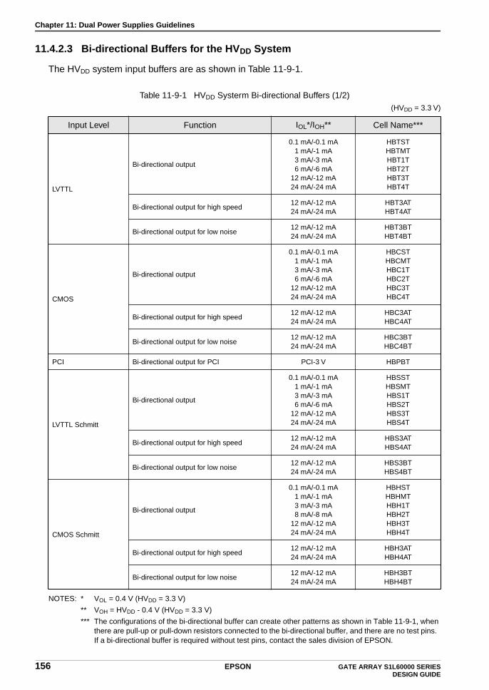
Chapter 11: Dual Power Supplies Guidelines
11.4.2.3 Bi-directional Buffers for the HVDD System
The HVDD system input buffers are as shown in Table 11-9-1.
NOTES: * VOL = 0.4 V (HVDD = 3.3 V)
** VOH = HVDD - 0.4 V (HVDD = 3.3 V)
*** The configurations of the bi-directional buffer can create other patterns as shown in Table 11-9-1, when there are pull-up or pull-down resistors connected to the bi-directional buffer, and there are no test pins. If a bi-directional buffer is required without test pins, contact the sales division of EPSON.
Table 11-9-1 HVDD Systerm Bi-directional Buffers (1/2)(HVDD = 3.3 V)
Input Level Function IOL*/IOH** Cell Name***
LVTTL
Bi-directional output
0.1 mA/-0.1 mA1 mA/-1 mA3 mA/-3 mA6 mA/-6 mA
12 mA/-12 mA24 mA/-24 mA
HBTSTHBTMTHBT1THBT2THBT3THBT4T
Bi-directional output for high speed12 mA/-12 mA24 mA/-24 mA
HBT3ATHBT4AT
Bi-directional output for low noise12 mA/-12 mA24 mA/-24 mA
HBT3BTHBT4BT
CMOS
Bi-directional output
0.1 mA/-0.1 mA1 mA/-1 mA3 mA/-3 mA6 mA/-6 mA
12 mA/-12 mA24 mA/-24 mA
HBCSTHBCMTHBC1THBC2THBC3THBC4T
Bi-directional output for high speed12 mA/-12 mA24 mA/-24 mA
HBC3ATHBC4AT
Bi-directional output for low noise12 mA/-12 mA24 mA/-24 mA
HBC3BTHBC4BT
PCI Bi-directional output for PCI PCI-3 V HBPBT
LVTTL Schmitt
Bi-directional output
0.1 mA/-0.1 mA1 mA/-1 mA3 mA/-3 mA6 mA/-6 mA
12 mA/-12 mA24 mA/-24 mA
HBSSTHBSMTHBS1THBS2THBS3THBS4T
Bi-directional output for high speed12 mA/-12 mA24 mA/-24 mA
HBS3ATHBS4AT
Bi-directional output for low noise12 mA/-12 mA24 mA/-24 mA
HBS3BTHBS4BT
CMOS Schmitt
Bi-directional output
0.1 mA/-0.1 mA1 mA/-1 mA3 mA/-3 mA8 mA/-8 mA
12 mA/-12 mA24 mA/-24 mA
HBHSTHBHMTHBH1THBH2THBH3THBH4T
Bi-directional output for high speed12 mA/-12 mA24 mA/-24 mA
HBH3ATHBH4AT
Bi-directional output for low noise12 mA/-12 mA24 mA/-24 mA
HBH3BTHBH4BT
156 EPSON GATE ARRAY S1L60000 SERIES DESIGN GUIDE
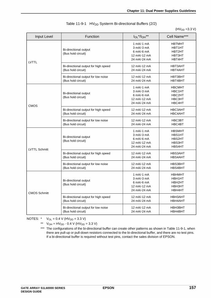
Chapter 11: Dual Power Supplies Guidelines
NOTES: * VOL = 0.4 V (HVDD = 3.3 V)
** VOH = HVDD - 0.4 V (HVDD = 3.3 V)
*** The configurations of the bi-directional buffer can create other patterns as shown in Table 11-9-1, when there are pull-up or pull-down resistors connected to the bi-directional buffer, and there are no test pins. If a bi-directional buffer is required without test pins, contact the sales division of EPSON.
Table 11-9-1 HVDD Systerm Bi-directional Buffers (2/2)(HVDD =3.3 V)
Input Level Function IOL*/IOH** Cell Name***
LVTTL
Bi-directional output(Bus hold circuit)
1 mA/-1 mA3 mA/-3 mA6 mA/-6 mA
12 mA/-12 mA24 mA/-24 mA
HBTMHTHBT1HTHBT2HTHBT3HTHBT4HT
Bi-directional output for high speed(Bus hold circuit)
12 mA/-12 mA24 mA/-24 mA
HBT3AHTHBT4AHT
Bi-directional output for low noise(Bus hold circuit)
12 mA/-12 mA24 mA/-24 mA
HBT3BHTHBT4BHT
CMOS
Bi-directional output(Bus hold circuit)
1 mA/-1 mA3 mA/-3 mA6 mA/-6 mA
12 mA/-12 mA24 mA/-24 mA
HBCMHTHBC1HTHBC2HTHBC3HTHBC4HT
Bi-directional output for high speed(Bus hold circuit)
12 mA/-12 mA24 mA/-24 mA
HBC3AHTHBC4AHT
Bi-directional output for low noise(Bus hold circuit)
12 mA/-12 mA24 mA/-24 mA
HBC3BTHBC4BT
LVTTL Schmitt
Bi-directional output(Bus hold circuit)
1 mA/-1 mA3 mA/-3 mA6 mA/-6 mA
12 mA/-12 mA24 mA/-24 mA
HBSMHTHBS1HTHBS2HTHBS3HTHBS4HT
Bi-directional output for high speed(Bus hold circuit)
12 mA/-12 mA24 mA/-24 mA
HBS3AHTHBS4AHT
Bi-directional output for low noise (Bus hold circuit)
12 mA/-12 mA24 mA/-24 mA
HBS3BHTHBS4BHT
CMOS Schmitt
Bi-directional output(Bus hold circuit)
1 mA/-1 mA3 mA/-3 mA6 mA/-6 mA
12 mA/-12 mA24 mA/-24 mA
HBHMHTHBH1HTHBH2HTHBH3HTHBH4HT
Bi-directional output for high speed(Bus hold circuit)
12 mA/-12 mA24 mA/-24 mA
HBH3AHTHBH4AHT
Bi-directional output for low noise(Bus hold circuit)
12 mA/-12 mA24 mA/-24 mA
HBH3BHTHBH4BHT
GATE ARRAY S1L60000 SERIES EPSON 157DESIGN GUIDE
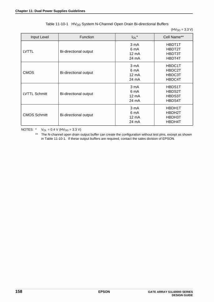
Chapter 11: Dual Power Supplies Guidelines
NOTES: * VOL = 0.4 V (HVDD = 3.3 V)
** The N-channel open drain output buffer can create the configuration without test pins, except as shown in Table 11-10-1. If these output buffers are required, contact the sales division of EPSON.
Table 11-10-1 HVDD System N-Channel Open Drain Bi-directional Buffers(HVDD = 3.3 V)
Input Level Function IOL* Cell Name**
LVTTL Bi-directional output
3 mA6 mA12 mA24 mA
HBDT1THBDT2THBDT3THBDT4T
CMOS Bi-directional output
3 mA6 mA12 mA24 mA
HBDC1THBDC2THBDC3THBDC4T
LVTTL Schmitt Bi-directional output
3 mA6 mA12 mA24 mA
HBDS1THBDS2THBDS3THBDS4T
CMOS Schmitt Bi-directional output
3 mA6 mA12 mA24 mA
HBDH1THBDH2THBDH3THBDH4T
158 EPSON GATE ARRAY S1L60000 SERIES DESIGN GUIDE
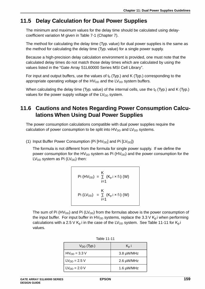
Chapter 11: Dual Power Supplies Guidelines
11.5 Delay Calculation for Dual Power Supplies
The minimum and maximum values for the delay time should be calculated using delay-coefficient variation M given in Table 7-1 (Chapter 7).
The method for calculating the delay time (Typ. value) for dual power supplies is the same as the method for calculating the delay time (Typ. value) for a single power supply.
Because a high-precision delay calculation environment is provided, one must note that the calculated delay times do not match those delay times which are calculated by using the values listed in the “Gate Array S1L60000 Series MSI Cell Library”.
For input and output buffers, use the values of t0 (Typ.) and K (Typ.) corresponding to the appropriate operating voltage of the HVDD and the LVDD system buffers.
When calculating the delay time (Typ. value) of the internal cells, use the t0 (Typ.) and K (Typ.) values for the power supply voltage of the LVDD system.
11.6 Cautions and Notes Regarding Power Consumption Calcu-lations When Using Dual Power Supplies
The power consumption calculations compatible with dual power supplies require the calculation of power consumption to be split into HVDD and LVDD systems.
(1) Input Buffer Power Consumption (Pi [HVDD] and Pi [LVDD])
The formula is not different from the formula for single power supply. If we define the power consumption for the HVDD system as Pi (HVDD) and the power consumption for the LVDD system as Pi (LVDD) then:
The sum of Pi (HVDD) and Pi (LVDD) from the formulas above is the power consumption of the input buffer. For input buffer in HVDD systems, replace the 3.3 V Kp i when performing calculations with a 2.5 V Kp i in the case of the LVDD system. See Table 11-11 for Kp i values.
Table 11-11
VDD (Typ.) Kp i
HVDD = 3.3 V 3.8 µW/MHz
LVDD = 2.5 V 2.6 µW/MHz
LVDD = 2.0 V 1.6 µW/MHz
Pi (HVDD) = ∑ (Kp i × f i) (W)
Pi (LVDD) = ∑ (Kp i × f i) (W)
i=1
i=1
K
K
GATE ARRAY S1L60000 SERIES EPSON 159DESIGN GUIDE

Chapter 11: Dual Power Supplies Guidelines
(2) Output Buffer Power Consumption (Po (HVDD) and Po (LVDD))
The formula is not different from the formula for single power supply. If we define the power consumption for the HVDD system as Po (HVDD) and the power consumption for the LVDD system as Po (LVDD) then
The output buffer power consumption is the sum of Po (HVDD) and Po (LVDD) of the formulas above. When performing these calculations, be aware that the VDD values in the HVDD and LVDD systems are different.
Note : Be aware that the value for VOH i is different in the HVDD system than it is in the LVDD system.
(3) Internal Cell Power Consumption (Pint)
This formula is not different from the formula for the single power supply.
The power consumption in the internal cells is calculated using the above formula.Replace Kpint with the appropriate LVDD Kpint when performing the calculation. See Table 9-2 of Chapter 9 for the Kpint values. Using the above, the Ptotal power consumpition is calculatption as follows.
Ptotal = Pi (HVDD) + Pi (LVDD) + Po (HVDD) + Po (LVDD) + Pint
Po (HVDD) = ∑ (PAC + PDC)
= ∑ f i × CL i × (HVDD)2 + ∑ ( HVDD - VOH i ) × | IOH i | × Duty H K
i=1
K
i=1
+ ∑ VOL i × IOL i × Duty L i=1
K
Po (LVDD) = ∑ (PAC + PDC)
= ∑ f i × CL i × (LVDD)2 + ∑ ( LVDD - VOH i ) × | IOH i | × Duty H
+ Σ VOL i × IOL i × Duty L
K K
Ki=1 i=1
i=1
= ∑ (Nb × U) × f i × Sp i × Kpint (W)K
i=1Pint
160 EPSON GATE ARRAY S1L60000 SERIES DESIGN GUIDE
Chapter 11: Dual Power Supplies Guidelines
11.7 Estimating the Number of Power Supply Pins When Using Dual Power Supplies
Even when using a dual power supply system, the magnitude of the allowable current per pair of power supplies (for both the HVDD and the LVDD system) is the same as for the single power supply case. Calculate the required number of power supplies separately for the HVDD system and the LVDD system.
*Assuming the current consumption of the HVDD system to be IDD (HVDD) [mA], the number of pairs of power supply pins NIDD (HVDD) for the current consumed IDD (HVDD) is given by:
NIDD (HVDD) ≥ IDD (HVDD)/50 (pairs): Possible to supply 50 mA fora pair of power supply
*Assuming the current consumption of the LVDD system to be IDD (LVDD) [mA], the number of pairs of power supply pins NIDD (LVDD) for the current consumed IDD (LVDD) is given by:
NIDD (LVDD) ≥ IDD (LVDD)/50 (pairs): Possible to supply 50 mA fora pair of power supply
In this case, there must be a minimum of two pairs of power supply pins for the HVDD system and a minimum of two pairs for the LVDD system.
NOTE: When adding power supplies in response to the simultaneous switching of outputs, distinctions should be drawn between the HVDD system output buffers and the LVDD system output buffers. Reference Chapter 10 (Table 10-1-1 to 10-2-2) when adding power supply systems for 2.5 V or 2.0 V system to each. Also, Reference Table 11-12 and 11-13) when adding power supply systems for 3.3 V system to each.
GATE ARRAY S1L60000 SERIES EPSON 161DESIGN GUIDE

Chapter 11: Dual Power Supplies Guidelines
Table 11-12 Number of Additional VSS Power Supplies Depending on the Simultaneous Operation of Output Buffers
(HVDD = 3.3 V)
Output DriveAbility (IOL)
Nuber of OutputBuffers OperatingSimultaneously
Number of Additional Power Supplies
CL≤50 pF CL≤100 pF CL≤200 pF
6 mA
≤8 0 1 2
≤16 1 2 3
≤24 1 2 4
≤32 2 3 5
12 mA
≤8 1 2 2
≤16 2 2 3
≤24 2 3 5
≤32 2 4 8
24 mA & PCI
≤8 2 3 4
≤16 3 4 6
≤24 4 6 8
≤32 6 8 16
Table 11-13 Number of Additional HVDD Power Supplies Depending on the Simultaneous Operation of Output Buffers
(HVDD = 3.3 V)
Output DriveAbility (IOH)
Nuber of OutputBuffers OperatingSimultaneously
Number of Additional Power Supplies
CL≤50 pF CL≤100 pF CL≤200 pF
6 mA
≤8 0 1 1
≤16 1 1 2
≤24 1 2 3
≤32 1 2 3
12 mA & PCI
≤8 1 2 2
≤16 2 2 3
≤24 2 3 3
≤32 3 3 6
24 mA
≤8 2 3 4
≤16 3 4 6
≤24 4 6 8
≤32 6 8 16
162 EPSON GATE ARRAY S1L60000 SERIES DESIGN GUIDE
Chapter 12: RAM (Clock Synchronous Type)
Chapter 12 RAM (Clock Synchronous Type)The S1L60000 series supports clock-synchronous RAM, in addition to the clock-asynchronous RAM described in Chapter 5. This type of RAM has latches in its chip select, write enable, address, and data input parts, allowing for clock-synchronized, high-speed operation.
12.1 Features
• Clock-synchronous 1-port and 2-port RAM are available.
• Memory contain latches in the chip select, write enable, address, and data input parts, allow-ing for clock-synchronized, high-speed operation.
• The data input and the data output ports are separated.
• Words can be configured from 16 to 256 words in 4-word increments, while bits can be con-figured between 1 to 32 bits in 1-bit increments.
• Maximum configuration: 8 Kbits per module
12.2 Word/Bit Configurations and Cell Names of the RAM
The delay parameters of the clock-synchronous RAM vary with its word/bit configurations. Therefore, Seiko Epson has cells corresponding to available individual word/bit configurations. When using the clock-synchronous RAM, please inform Seiko Epson whether the RAM used is 1-port or 2-port and how it is word/bit-configured.
The cell names available for the typical word/bit configurations of 1-port and 2-port RAM sticks are listed on Tables 12-1 and 12-2 , respectively. The cell names for synchronous RAM sticks are assigned by the naming rules described below according to the Word/Bit Configurations.
1-port RAM "SJ XXX YY"
2-port RAM "SK XXX YY" XXX: Number of words (hex), YY: Number of bits (hex)
If any synchronous RAM whose word/bit configurations exceed the acceptable range is required, use multiple instances of synchronous RAM in combination as needed for the intended application.
Table 12-1 Cell Names Available for Various Word/Bit Configurations of 1-port RAM (Clock Synchronous Type)
64Word 128Word 192Word 256Word
8Bit SJ04008 SJ08008 SJ0C008 SJ10008
16Bit SJ04010 SJ08010 SJ0C010 SJ10010
24Bit SJ04018 SJ08018 SJ0C018 SJ10018
32Bit SJ04020 SJ08020 SJ0C020 SJ10020
GATE ARRAY S1L60000 SERIES EPSON 163DESIGN GUIDE
Chapter 12: RAM (Clock Synchronous Type)
Table 12-2 Cell Names Available for Various Word/Bit Configurations of 2-port RAM (Clock Synchronous Type)
12.3 Number of Basic Cells for Synchronous RAM
The RAM sizes in the X and Y directions and the number of basic cells used are calculated using the following equations, respectively.
(1) 1-port RAM
Size in X direction: RX = 27 + 7 × number of words / 4 + 8
Size in Y direction: RY = α + 7 × number of bits × 2 + 2
Number of basic cells: RAMBCS=RX × RY
Note that α = 3 when 16 ≤ number of words ≤ 32, or 4 when 36 ≤ number of words ≤ 256.
Table 12-3 Typical Configuration of 1-port RAM and Number of Basic Cells
(2) 2-port RAM
Size in X direction: RX = 27 + 7 × number of words / 4 + 8
Size in Y direction: RY = α + 7 × number of bits × 2 + 2
Number of basic cells: RAMBCS=RX × RY
Note that α = 4 when 16 ≤ number of words ≤ 32, or 6 when 36 ≤ number of words ≤ 256.
64Word 128Word 192Word 256Word
8Bit SK04008 SK08008 SK0C008 SK10008
16Bit SK04010 SK08010 SK0C010 SK10010
24Bit SK04018 SK08018 SK0C018 SK10018
32Bit SK04020 SK08020 SK0C020 SK10020
8Bit 16Bit 24Bit 32Bit
32Word 2,548 4,004 5,460 6,916
64Word 4,263 6,615 8,967 11,319
128Word 7,511 11,655 15,799 19,943
256Word 14,007 21,735 29,463 37,191
164 EPSON GATE ARRAY S1L60000 SERIES DESIGN GUIDE

Chapter 12: RAM (Clock Synchronous Type)
Table 12-4 Typical Configuration of 2-port RAM and Number of Basic Cells
12.4 Investigating RAM Placement on Master Slice
To determine whether the RAM (Clock Synchronous Type) can be mounted on each master, refer to the description in Section 5.4.
8Bit 16Bit 24Bit 32Bit
32Word 2,552 3,960 5,368 6,776
64Word 4,464 6,768 9,072 11,376
128Word 7,936 12,032 16,128 20,224
256Word 14,880 22,560 30,240 37,920
GATE ARRAY S1L60000 SERIES EPSON 165DESIGN GUIDE
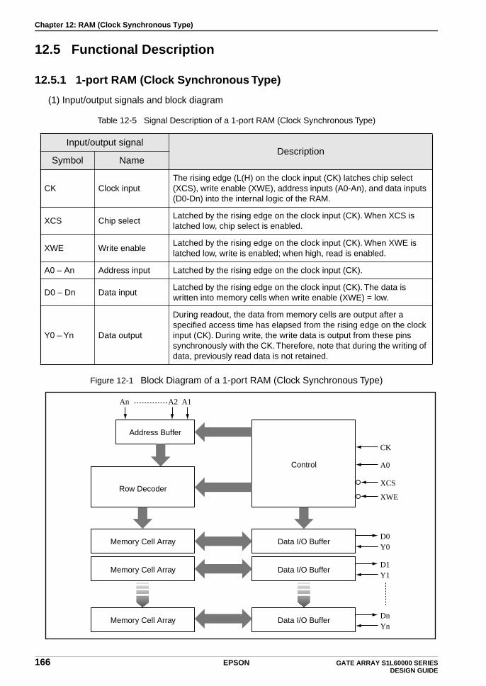
Chapter 12: RAM (Clock Synchronous Type)
12.5 Functional Description
12.5.1 1-port RAM (Clock Synchronous Type)
(1) Input/output signals and block diagram
Table 12-5 Signal Description of a 1-port RAM (Clock Synchronous Type)
Figure 12-1 Block Diagram of a 1-port RAM (Clock Synchronous Type)
Input/output signalDescription
Symbol Name
CK Clock inputThe rising edge (L(H) on the clock input (CK) latches chip select (XCS), write enable (XWE), address inputs (A0-An), and data inputs (D0-Dn) into the internal logic of the RAM.
XCS Chip selectLatched by the rising edge on the clock input (CK). When XCS is latched low, chip select is enabled.
XWE Write enableLatched by the rising edge on the clock input (CK). When XWE is latched low, write is enabled; when high, read is enabled.
A0 – An Address input Latched by the rising edge on the clock input (CK).
D0 – Dn Data inputLatched by the rising edge on the clock input (CK). The data is written into memory cells when write enable (XWE) = low.
Y0 – Yn Data output
During readout, the data from memory cells are output after a specified access time has elapsed from the rising edge on the clock input (CK). During write, the write data is output from these pins synchronously with the CK. Therefore, note that during the writing of data, previously read data is not retained.
Data I/O BufferMemory Cell Array
Data I/O BufferMemory Cell Array
Data I/O BufferMemory Cell Array
Address Buffer
Control
Row Decoder
DnYn
D1Y1
D0Y0
A0
An A1A2
CK
XCS
XWE
166 EPSON GATE ARRAY S1L60000 SERIES DESIGN GUIDE

Chapter 12: RAM (Clock Synchronous Type)
(2) Circuit operation
To write to the RAM, enable (L) chip select (XCS) and write enable (XWE) and then setting address inputs (A0-An) and data inputs (D0-Dn) before the clock input (CK) increases. When the clock input increases, all of the chip select, write enable, address inputs, and data inputs are latched, thereby initializing a write operation. The write data is output from the data output pins (Y0-Yn) until the next time the clock input increases.
To read from the RAM, enable (L) chip select (XCS) and disable (H) write enable (XWE), and then setting address inputs (A0-An) before the clock input (CK) increases. When the clock input increases, all of the chip select, write enable, and address inputs are latched, thereby initializing a read operation. During this period, data is sent out from the output pins (Y0-Yn) after a specified access time has elapsed from the rising edge on the clock input.
Table 12-6 Truth Table for Operation of 1-port RAM (Clock Synchronous Type)
12.5.2 2-port RAM (Clock Synchronous Type)
(1) Input/output signals and block diagram
The first port is write-only, and the second port is read-only. The RAM has a clock input pin for each port, which can be operated independently with given frequencies and timings.
If write enable (XWA) for the first port and read enable (XRB) for the second port both are latched high, the RAM is in standby.
Table 12-7 Signal Description of 2-port RAM (Clock Synchronous Type)
Signals for the first port (write only)
CK XCS XWE Output status‘ Operation mode
L → H L H Read Data Read
L → H L L Write Data Write
L → H H L or H Data Hold Standby
Input/output signalDescription
Symbol Name
CKA Clock inputThe rising edge (L(H) on the clock input (CKA) latches write enable (XWA), address inputs (AA0-AAn), and data inputs (D0-Dn) into the internal logic of the RAM.
XWA Write enableLatched by the rising edge on the clock input (CKA). When XWE is latched low, a write operation starts.
AA0 – AAn Address input Latched by the rising edge on the clock input (CKA)
D0 – Dn Data inputLatched by the rising edge on the clock input (CKA). When write enable (XWA) = low, data is written into memory cells.
GATE ARRAY S1L60000 SERIES EPSON 167DESIGN GUIDE

Chapter 12: RAM (Clock Synchronous Type)
Signals for the second port (read only)
Figure 12-2 Block Diagram of a 2-port RAM (Clock Synchronous Type)
(2) Circuit operation
To write to the RAM, enable (L) write enable (XWA) and then setting address inputs (AA0-AAn) and data inputs (D0-Dn) before the clock input (CKA) increases. When the clock input (CKA) increases, all of the write enable (XWA), address inputs (AA0-AAn), and data inputs (D0-Dn) are latched, thereby initializing a write operation.
To read from the RAM, enable (L) read enable (XRB) and then setting address inputs (AB0-ABn) before the clock input (CKB) increases. When the clock input (CKB) increases, all of the read enable (XRB) and address inputs (AB0-ABn) are latched, thereby initializing a read operation. During this period, data is sent out from the output pins (Y0-Yn), after a specified access time has elapsed, from the rising edge on the clock input (CKB).
Input/output signalDescription
Symbol Name
CKB Clock inputThe rising edge (L(H) on the clock input (CKB) latches read enable (XRB) and address inputs (AB0-ABn) into the internal logic of the RAM.
XRB Read enableLatched by the rising edge on the clock input (CKB). When XRB is latched low, a read operation starts.
AB0 – ABn Address input Latched by the rising edge on the clock input (CKB).
Y0 – Yn Data outputData from memory cells are output, after a specified access time has elapsed, from the rising edge of the clock input (CKB).
Data I/O Buffer
Memory Cell Array
Add
ress
Buf
fer
Add
ress
Buf
fer
Row
Dec
oder
Row
Dec
oder
Port 1Control
Port 2Control
AA0
CKA
AA1
AA2
AAn
XWA
AB0
CKB
AB1
AB2
ABn
XRB
Y0 Yn DnD0
168 EPSON GATE ARRAY S1L60000 SERIES DESIGN GUIDE

Chapter 12: RAM (Clock Synchronous Type)
Table 12-8 Truth Table for Operation of 2-port RAM (Clock Synchronous Type)
(Truth table for operation of the first port (write only))
(Truth table for operation of the second port (read only)
If a write to and a read from are simultaneously attempted for the same memory, the write operation is given priority. Data is written to the memory normally, but no result is returned for the read data request.
CKA XWA Operation mode
L → H H Standby
L → H L Write
CKB XRB Output status Operation mode
L → H H Data Hold Standby
L → H L Read Data Read
GATE ARRAY S1L60000 SERIES EPSON 169DESIGN GUIDE
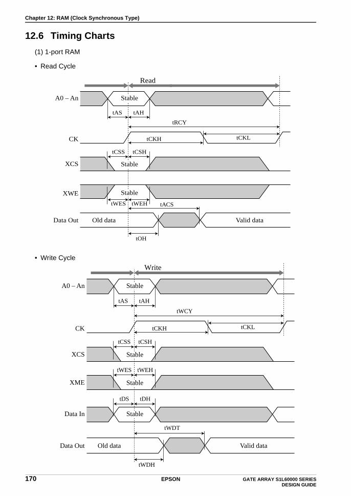
Chapter 12: RAM (Clock Synchronous Type)
12.6 Timing Charts
(1) 1-port RAM
• Read Cycle
• Write Cycle
Stable
Stable
Stable
tAS
tCSS tCSH
tWES tWEH
tOH
tAH
tCKH
tACS
tRCY
Read
tCKL
A0 – An
CK
XCS
XWE
Data Out Old data Valid data
tWDT
tWDH
Data Out Old data Valid data
Stable
Write
Stable
tAS
tCSS tCSH
tAH
tCKH
tWCY
tCKL
A0 – An
StableData In
CK
XCS
Stable
tWES tWEH
tDS tDH
XME
170 EPSON GATE ARRAY S1L60000 SERIES DESIGN GUIDE

Chapter 12: RAM (Clock Synchronous Type)
(2) 2-port RAM
• First port
• Second port
Stable
Write
Stable
tAS
tWAS tWAH
tDS tDH
tAH
tCKH
tWCY
tCKL
AA0 – AAn
StableData In
CKA
XWA
tOH
tACC
Stable
Read
Stable
tAS
tRBS tRBH
tAH
tCKH
tRCY
tCKL
AB0 – ABn
CKB
XRB
Data Out Old data Valid data
GATE ARRAY S1L60000 SERIES EPSON 171DESIGN GUIDE
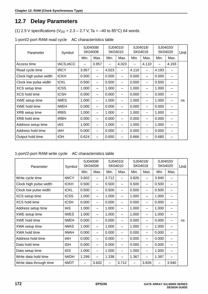
Chapter 12: RAM (Clock Synchronous Type)
12.7 Delay Parameters
(1) 2.5 V specifications (VDD = 2.3 – 2.7 V, Ta = –40 to 85°C) 64 words
1-port/2-port RAM read cycle AC characteristics table
1-port/2-port RAM write cycle AC characteristics table
Parameter SymbolSJ04008/SK04008
SJ04010/SK04010
SJ04018/SK04018
SJ04020/SK04020 Unit
Min. Max. Min. Max. Min. Max. Min. Max.
Access time tACS,tACC – 3.957 – 4.023 – 4.110 – 4.193
ns
Read cycle time tRCY 3.957 – 4.023 – 4.110 – 4.193 –
Clock high pulse width tCKH 0.500 – 0.500 – 0.500 – 0.500 –
Clock low pulse width tCKL 0.500 – 0.500 – 0.500 – 0.500 –
XCS setup time tCSS 1.000 – 1.000 – 1.000 – 1.000 –
XCS hold time tCSH 0.000 – 0.000 – 0.000 – 0.000 –
XWE setup time tWES 1.000 – 1.000 – 1.000 – 1.000 –
XWE hold time tWEH 0.000 – 0.000 – 0.000 – 0.000 –
XRB setup time tRBS 1.000 – 1.000 – 1.000 – 1.000 –
XRB hold time tRBH 0.000 – 0.000 – 0.000 – 0.000 –
Address setup time tAS 1.000 – 1.000 – 1.000 – 1.000 –
Address hold time tAH 0.000 – 0.000 – 0.000 – 0.000 –
Output hold time tOH 0.624 – 0.650 – 0.666 – 0.680 –
Parameter SymbolSJ04008/SK04008
SJ04010/SK04010
SJ04018/SK04018
SJ04020/SK04020 Unit
Min. Max. Min. Max. Min. Max. Min Max.
Write cycle time tWCY 3.602 – 3.712 – 3.826 – 3.940 –
ns
Clock high pulse width tCKH 0.500 – 0.500 – 0.500 – 0.500 –
Clock low pulse width tCKL 0.500 – 0.500 – 0.500 – 0.500 –
XCS setup time tCSS 1.000 – 1.000 – 1.000 – 1.000 –
XCS hold time tCSH 0.000 – 0.000 – 0.000 – 0.000 –
Address setup time tAS 1.000 – 1.000 – 1.000 – 1.000 –
XWE setup time tWES 1.000 – 1.000 – 1.000 – 1.000 –
XWE hold time tWEH 0.000 – 0.000 – 0.000 – 0.000 –
XWA setup time tWAS 1.000 – 1.000 – 1.000 – 1.000 –
XWA hold time tWAH 0.000 – 0.000 – 0.000 – 0.000 –
Address hold time tAH 0.000 – 0.000 – 0.000 – 0.000 –
Data hold time tDH 0.000 – 0.000 – 0.000 – 0.000 –
Data setup time tDS 1.000 – 1.000 – 1.000 – 1.000 –
Write data hold time tWDH 1.299 – 1.338 – 1.367 – 1.397 –
Write data through time tWDT – 3.602 – 3.712 – 3.826 – 3.940
172 EPSON GATE ARRAY S1L60000 SERIES DESIGN GUIDE

Chapter 12: RAM (Clock Synchronous Type)
(2) 2.5 V specifications (VDD = 2.3 – 2.7 V, Ta = 0 to 70°C) 64 words
1-port/2-port RAM read cycle AC characteristics table
1-port/2-port RAM write cycle AC characteristics table
Parameter SymbolSJ04008/SK04008
SJ04010/SK04010
SJ04018/SK04018
SJ04020/SK04020 Unit
Min. Max. Min. Max. Min. Max. Min. Max.
Access time tACS,tACC – 3.743 – 3.806 – 3.887 – 3.966
ns
Read cycle time tRCY 3.743 – 3.806 – 3.887 – 3.966 –
Clock high pulse width tCKH 0.500 – 0.500 – 0.500 – 0.500 –
Clock low pulse width tCKL 0.500 – 0.500 – 0.500 – 0.500 –
XCS setup time tCSS 1.000 – 1.000 – 1.000 – 1.000 –
XCS hold time tCSH 0.000 – 0.000 – 0.000 – 0.000 –
XWE setup time tWES 1.000 – 1.000 – 1.000 – 1.000 –
XWE hold time tWEH 0.000 – 0.000 – 0.000 – 0.000 –
XRB setup time tRBS 1.000 – 1.000 – 1.000 – 1.000 –
XRB hold time tRBH 0.000 – 0.000 – 0.000 – 0.000 –
Address setup time tAS 1.000 – 1.000 – 1.000 – 1.000 –
Address hold time tAH 0.000 – 0.000 – 0.000 – 0.000 –
Output hold time tOH 0.669 – 0.696 – 0.713 – 0.728 –
Parameter SymbolSJ04008/SK04008
SJ04010/SK04010
SJ04018/SK04018
SJ04020/SK04020 Unit
Min. Max. Min. Max. Min. Max. Min. Max.
Write cycle time tWCY 3.407 – 3.512 – 3.619 – 3.727 –
ns
Clock high pulse width tCKH 0.500 – 0.500 – 0.500 – 0.500 –
Clock low pulse width tCKL 0.500 – 0.500 – 0.500 – 0.500 –
XCS setup time tCSS 1.000 – 1.000 – 1.000 – 1.000 –
XCS hold time tCSH 0.000 – 0.000 – 0.000 – 0.000 –
Address setup time tAS 1.000 – 1.000 – 1.000 – 1.000 –
XWE setup time tWES 1.000 – 1.000 – 1.000 – 1.000 –
XWE hold time tWEH 0.000 – 0.000 – 0.000 – 0.000 –
XWA setup time tWAS 1.000 – 1.000 – 1.000 – 1.000 –
XWA hold time tWAH 0.000 – 0.000 – 0.000 – 0.000 –
Address hold time tAH 0.000 – 0.000 – 0.000 – 0.000 –
Data hold time tDH 0.000 – 0.000 – 0.000 – 0.000 –
Data setup time tDS 1.000 – 1.000 – 1.000 – 1.000 –
Write data hold time tWDH 1.391 – 1.433 – 1.465 – 1.497 –
Write data through time tWDT – 3.407 – 3.512 – 3.619 – 3.727
GATE ARRAY S1L60000 SERIES EPSON 173DESIGN GUIDE

Chapter 12: RAM (Clock Synchronous Type)
(3) 2.5 V specifications (VDD = 2.3 – 2.7 V, Ta = –40 to 85°C) 128 words
1-port/2-port RAM read cycle AC characteristics table
1-port/2-port RAM write cycle AC characteristics table
Parameter SymbolSJ08008/SK08008
SJ08010/SK08010
SJ08018/SK08018
SJ08020/SK08020 Unit
Min. Max. Min. Max. Min. Max. Min. Max.
Access time tACS,tACC – 4.995 – 5.060 – 5.132 – 5.241
ns
Read cycle time tRCY 4.995 – 5.060 – 5.132 – 5.241 –
Clock high pulse width tCKH 0.500 – 0.500 – 0.500 – 0.500 –
Clock low pulse width tCKL 0.500 – 0.500 – 0.500 – 0.500 –
XCS setup time tCSS 1.000 – 1.000 – 1.000 – 1.000 –
XCS hold time tCSH 0.000 – 0.000 – 0.000 – 0.000 –
XWE setup time tWES 1.000 – 1.000 – 1.000 – 1.000 –
XWE hold time tWEH 0.000 – 0.000 – 0.000 – 0.000 –
XRB setup time tRBS 1.000 – 1.000 – 1.000 – 1.000 –
XRB hold time tRBH 0.000 – 0.000 – 0.000 – 0.000 –
Address setup time tAS 1.000 – 1.000 – 1.000 – 1.000 –
Address hold time tAH 0.000 – 0.000 – 0.000 – 0.000 –
Output hold time tOH 0.641 – 0.659 – 0.675 – 0.693 –
Parameter SymbolSJ08008/SK08008
SJ08010/SK08010
SJ08018/SK08018
SJ08020/SK08020 Unit
Min. Max. Min. Max. Min. Max. Min. Max.
Write cycle time tWCY 3.685 – 3.807 – 3.909 – 4.018 –
ns
Clock high pulse width tCKH 0.500 – 0.500 – 0.500 – 0.500 –
Clock low pulse width tCKL 0.500 – 0.500 – 0.500 – 0.500 –
XCS setup time tCSS 1.000 – 1.000 – 1.000 – 1.000 –
XCS hold time tCSH 0.000 – 0.000 – 0.000 – 0.000 –
Address setup time tAS 1.000 – 1.000 – 1.000 – 1.000 –
XWE setup time tWES 1.000 – 1.000 – 1.000 – 1.000 –
XWE hold time tWEH 0.000 – 0.000 – 0.000 – 0.000 –
XWA setup time tWAS 1.000 – 1.000 – 1.000 – 1.000 –
XWA hold time tWAH 0.000 – 0.000 – 0.000 – 0.000 –
Address hold time tAH 0.000 – 0.000 – 0.000 – 0.000 –
Data hold time tDH 0.000 – 0.000 – 0.000 – 0.000 –
Data setup time tDS 1.000 – 1.000 – 1.000 – 1.000 –
Write data hold time tWDH 1.341 – 1.376 – 1.426 – 1.433 –
Write data through time tWDT – 3.685 – 3.807 – 3.909 – 4.018
174 EPSON GATE ARRAY S1L60000 SERIES DESIGN GUIDE
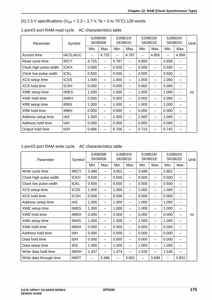
Chapter 12: RAM (Clock Synchronous Type)
(4) 2.5 V specifications (VDD = 2.3 – 2.7 V, Ta = 0 to 70°C) 128 words
1-port/2-port RAM read cycle AC characteristics table
1-port/2-port RAM write cycle AC characteristics table
Parameter SymbolSJ08008/SK08008
SJ08010/SK08010
SJ08018/SK08018
SJ08020/SK08020 Unit
Min. Max. Min. Max. Min. Max. Min. Max.
Access time tACS,tACC – 4.725 – 4.787 – 4.855 – 4.958
ns
Read cycle time tRCY 4.725 – 4.787 – 4.855 – 4.958 –
Clock high pulse width tCKH 0.500 – 0.500 – 0.500 – 0.500 –
Clock low pulse width tCKL 0.500 – 0.500 – 0.500 – 0.500 –
XCS setup time tCSS 1.000 – 1.000 – 1.000 – 1.000 –
XCS hold time tCSH 0.000 – 0.000 – 0.000 – 0.000 –
XWE setup time tWES 1.000 – 1.000 – 1.000 – 1.000 –
XWE hold time tWEH 0.000 – 0.000 – 0.000 – 0.000 –
XRB setup time tRBS 1.000 – 1.000 – 1.000 – 1.000 –
XRB hold time tRBH 0.000 – 0.000 – 0.000 – 0.000 –
Address setup time tAS 1.000 – 1.000 – 1.000 – 1.000 –
Address hold time tAH 0.000 – 0.000 – 0.000 – 0.000 –
Output hold time tOH 0.686 – 0.706 – 0.723 – 0.742 –
Parameter SymbolSJ08008/SK08008
SJ08010/SK08010
SJ08018/SK08018
SJ08020/SK08020 Unit
Min. Max. Min. Max. Min. Max. Min. Max.
Write cycle time tWCY 3.486 – 3.601 – 3.698 – 3.801 –
ns
Clock high pulse width tCKH 0.500 – 0.500 – 0.500 – 0.500 –
Clock low pulse width tCKL 0.500 – 0.500 – 0.500 – 0.500 –
XCS setup time tCSS 1.000 – 1.000 – 1.000 – 1.000 –
XCS hold time tCSH 0.000 – 0.000 – 0.000 – 0.000 –
Address setup time tAS 1.000 – 1.000 – 1.000 – 1.000 –
XWE setup time tWES 1.000 – 1.000 – 1.000 – 1.000 –
XWE hold time tWEH 0.000 – 0.000 – 0.000 – 0.000 –
XWA setup time tWAS 1.000 – 1.000 – 1.000 – 1.000 –
XWA hold time tWAH 0.000 – 0.000 – 0.000 – 0.000 –
Address hold time tAH 0.000 – 0.000 – 0.000 – 0.000 –
Data hold time tDH 0.000 – 0.000 – 0.000 – 0.000 –
Data setup time tDS 1.000 – 1.000 – 1.000 – 1.000 –
Write data hold time tWDH 1.437 – 1.474 – 1.528 – 1.536 –
Write data through time tWDT – 3.486 – 3.601 – 3.698 – 3.801
GATE ARRAY S1L60000 SERIES EPSON 175DESIGN GUIDE
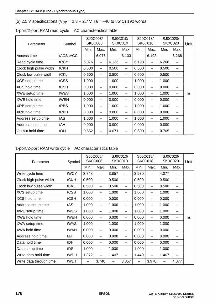
Chapter 12: RAM (Clock Synchronous Type)
(5) 2.5 V specifications (VDD = 2.3 – 2.7 V, Ta = –40 to 85°C) 192 words
1-port/2-port RAM read cycle AC characteristics table
1-port/2-port RAM write cycle AC characteristics table
Parameter SymbolSJ0C008/SK0C008
SJ0C010/SK0C010
SJ0C018/SK0C018
SJ0C020/SK0C020 Unit
Min. Max. Min. Max. Min. Max. Min. Max.
Access time tACS,tACC – 6.076 – 6.133 – 6.198 – 6.268
ns
Read cycle time tRCY 6.076 – 6.133 – 6.198 – 6.268 –
Clock high pulse width tCKH 0.500 – 0.500 – 0.500 – 0.500 –
Clock low pulse width tCKL 0.500 – 0.500 – 0.500 – 0.500 –
XCS setup time tCSS 1.000 – 1.000 – 1.000 – 1.000 –
XCS hold time tCSH 0.000 – 0.000 – 0.000 – 0.000 –
XWE setup time tWES 1.000 – 1.000 – 1.000 – 1.000 –
XWE hold time tWEH 0.000 – 0.000 – 0.000 – 0.000 –
XRB setup time tRBS 1.000 – 1.000 – 1.000 – 1.000 –
XRB hold time tRBH 0.000 – 0.000 – 0.000 – 0.000 –
Address setup time tAS 1.000 – 1.000 – 1.000 – 1.000 –
Address hold time tAH 0.000 – 0.000 – 0.000 – 0.000 –
Output hold time tOH 0.652 – 0.671 – 0.690 – 0.705 –
Parameter SymbolSJ0C008/SK0C008
SJ0C010/SK0C010
SJ0C018/SK0C018
SJ0C020/SK0C020 Unit
Min. Max. Min. Max. Min. Max. Min. Max.
Write cycle time tWCY 3.748 – 3.857 – 3.970 – 4.077 –
ns
Clock high pulse width tCKH 0.500 – 0.500 – 0.500 – 0.500 –
Clock low pulse width tCKL 0.500 – 0.500 – 0.500 – 0.500 –
XCS setup time tCSS 1.000 – 1.000 – 1.000 – 1.000 –
XCS hold time tCSH 0.000 – 0.000 – 0.000 – 0.000 –
Address setup time tAS 1.000 – 1.000 – 1.000 – 1.000 –
XWE setup time tWES 1.000 – 1.000 – 1.000 – 1.000 –
XWE hold time tWEH 0.000 – 0.000 – 0.000 – 0.000 –
XWA setup time tWAS 1.000 – 1.000 – 1.000 – 1.000 –
XWA hold time tWAH 0.000 – 0.000 – 0.000 – 0.000 –
Address hold time tAH 0.000 – 0.000 – 0.000 – 0.000 –
Data hold time tDH 0.000 – 0.000 – 0.000 – 0.000 –
Data setup time tDS 1.000 – 1.000 – 1.000 – 1.000 –
Write data hold time tWDH 1.372 – 1.407 – 1.440 – 1.467 –
Write data through time tWDT – 3.748 – 3.857 – 3.970 – 4.077
176 EPSON GATE ARRAY S1L60000 SERIES DESIGN GUIDE

Chapter 12: RAM (Clock Synchronous Type)
(6) 2.5 V specifications (VDD = 2.3 – 2.7 V, Ta = 0 to 70°C) 192 words
1-port/2-port RAM read cycle AC characteristics table
1-port/2-port RAM write cycle AC characteristics table
Parameter SymbolSJ0C008/SK0C008
SJ0C010/SK0C010
SJ0C018/SK0C018
SJ0C020/SK0C020 Unit
Min. Max. Min. Max. Min. Max. Min. Max.
Access time tACS,tACC – 5.748 – 5.802 – 5.863 – 5.929
ns
Read cycle time tRCY 5.748 – 5.802 – 5.863 – 5.929 –
Clock high pulse width tCKH 0.500 – 0.500 – 0.500 – 0.500 –
Clock low pulse width tCKL 0.500 – 0.500 – 0.500 – 0.500 –
XCS setup time tCSS 1.000 – 1.000 – 1.000 – 1.000 –
XCS hold time tCSH 0.000 – 0.000 – 0.000 – 0.000 –
XWE setup time tWES 1.000 – 1.000 – 1.000 – 1.000 –
XWE hold time tWEH 0.000 – 0.000 – 0.000 – 0.000 –
XRB setup time tRBS 1.000 – 1.000 – 1.000 – 1.000 –
XRB hold time tRBH 0.000 – 0.000 – 0.000 – 0.000 –
Address setup time tAS 1.000 – 1.000 – 1.000 – 1.000 –
Address hold time tAH 0.000 – 0.000 – 0.000 – 0.000 –
Output hold time tOH 0.698 – 0.719 – 0.739 – 0.756 –
Parameter SymbolSJ0C008/SK0C008
SJ0C010/SK0C010
SJ0C018/SK0C018
SJ0C020/SK0C020 Unit
Min. Max. Min. Max. Min. Max. Min. Max.
Write cycle time tWCY 3.546 – 3.649 – 3.755 – 3.857 –
ns
Clock high pulse width tCKH 0.500 – 0.500 – 0.500 – 0.500 –
Clock low pulse width tCKL 0.500 – 0.500 – 0.500 – 0.500 –
XCS setup time tCSS 1.000 – 1.000 – 1.000 – 1.000 –
XCS hold time tCSH 0.000 – 0.000 – 0.000 – 0.000 –
Address setup time tAS 1.000 – 1.000 – 1.000 – 1.000 –
XWE setup time tWES 1.000 – 1.000 – 1.000 – 1.000 –
XWE hold time tWEH 0.000 – 0.000 – 0.000 – 0.000 –
XWA setup time tWAS 1.000 – 1.000 – 1.000 – 1.000 –
XWA hold time tWAH 0.000 – 0.000 – 0.000 – 0.000 –
Address hold time tAH 0.000 – 0.000 – 0.000 – 0.000 –
Data hold time tDH 0.000 – 0.000 – 0.000 – 0.000 –
Data setup time tDS 1.000 – 1.000 – 1.000 – 1.000 –
Write data hold time tWDH 1.470 – 1.507 – 1.543 – 1.572 –
Write data through time tWDT – 3.546 – 3.649 – 3.755 – 3.857
GATE ARRAY S1L60000 SERIES EPSON 177DESIGN GUIDE
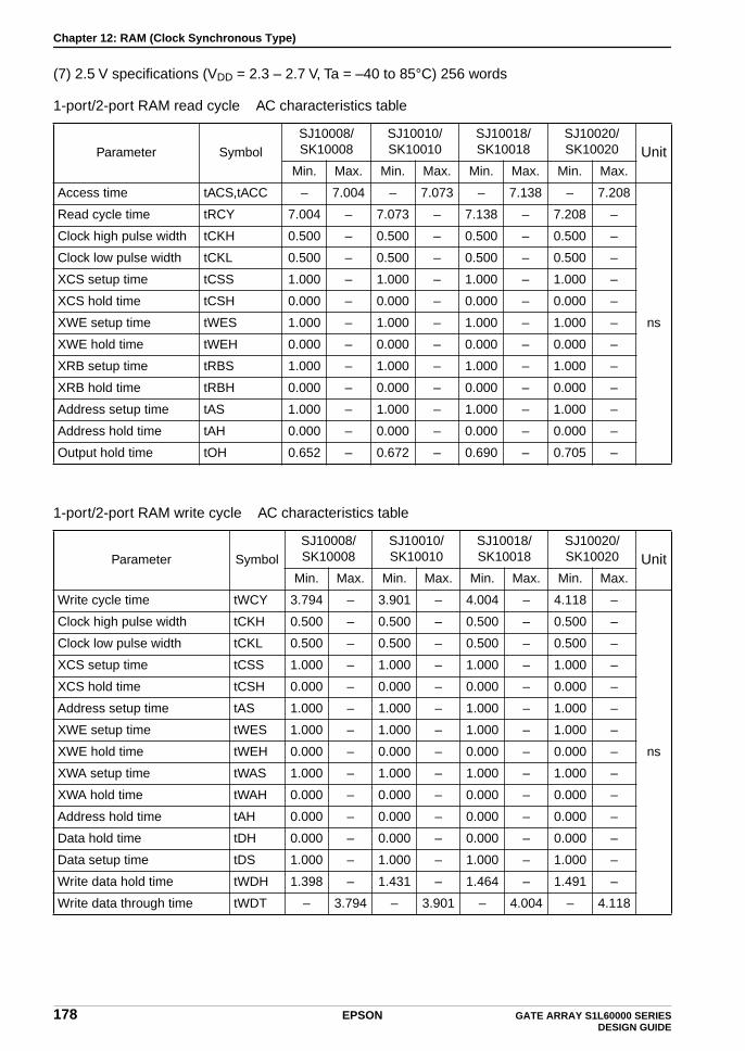
Chapter 12: RAM (Clock Synchronous Type)
(7) 2.5 V specifications (VDD = 2.3 – 2.7 V, Ta = –40 to 85°C) 256 words
1-port/2-port RAM read cycle AC characteristics table
1-port/2-port RAM write cycle AC characteristics table
Parameter SymbolSJ10008/SK10008
SJ10010/SK10010
SJ10018/SK10018
SJ10020/SK10020 Unit
Min. Max. Min. Max. Min. Max. Min. Max.
Access time tACS,tACC – 7.004 – 7.073 – 7.138 – 7.208
ns
Read cycle time tRCY 7.004 – 7.073 – 7.138 – 7.208 –
Clock high pulse width tCKH 0.500 – 0.500 – 0.500 – 0.500 –
Clock low pulse width tCKL 0.500 – 0.500 – 0.500 – 0.500 –
XCS setup time tCSS 1.000 – 1.000 – 1.000 – 1.000 –
XCS hold time tCSH 0.000 – 0.000 – 0.000 – 0.000 –
XWE setup time tWES 1.000 – 1.000 – 1.000 – 1.000 –
XWE hold time tWEH 0.000 – 0.000 – 0.000 – 0.000 –
XRB setup time tRBS 1.000 – 1.000 – 1.000 – 1.000 –
XRB hold time tRBH 0.000 – 0.000 – 0.000 – 0.000 –
Address setup time tAS 1.000 – 1.000 – 1.000 – 1.000 –
Address hold time tAH 0.000 – 0.000 – 0.000 – 0.000 –
Output hold time tOH 0.652 – 0.672 – 0.690 – 0.705 –
Parameter SymbolSJ10008/SK10008
SJ10010/SK10010
SJ10018/SK10018
SJ10020/SK10020 Unit
Min. Max. Min. Max. Min. Max. Min. Max.
Write cycle time tWCY 3.794 – 3.901 – 4.004 – 4.118 –
ns
Clock high pulse width tCKH 0.500 – 0.500 – 0.500 – 0.500 –
Clock low pulse width tCKL 0.500 – 0.500 – 0.500 – 0.500 –
XCS setup time tCSS 1.000 – 1.000 – 1.000 – 1.000 –
XCS hold time tCSH 0.000 – 0.000 – 0.000 – 0.000 –
Address setup time tAS 1.000 – 1.000 – 1.000 – 1.000 –
XWE setup time tWES 1.000 – 1.000 – 1.000 – 1.000 –
XWE hold time tWEH 0.000 – 0.000 – 0.000 – 0.000 –
XWA setup time tWAS 1.000 – 1.000 – 1.000 – 1.000 –
XWA hold time tWAH 0.000 – 0.000 – 0.000 – 0.000 –
Address hold time tAH 0.000 – 0.000 – 0.000 – 0.000 –
Data hold time tDH 0.000 – 0.000 – 0.000 – 0.000 –
Data setup time tDS 1.000 – 1.000 – 1.000 – 1.000 –
Write data hold time tWDH 1.398 – 1.431 – 1.464 – 1.491 –
Write data through time tWDT – 3.794 – 3.901 – 4.004 – 4.118
178 EPSON GATE ARRAY S1L60000 SERIES DESIGN GUIDE

Chapter 12: RAM (Clock Synchronous Type)
(8) 2.5 V specifications (VDD = 2.3 – 2.7 V, Ta = 0 to 70°C) 256 words
1-port/2-port RAM read cycle AC characteristics table
1-port/2-port RAM write cycle AC characteristics table
Parameter SymbolSJ10008/SK10008
SJ10010/SK10010
SJ10018/SK10018
SJ10020/SK10020 Unit
Min. Max. Min. Max. Min. Max. Min. Max.
Access time tACS,tACC – 6.626 – 6.690 – 6.752 – 6.818
ns
Read cycle time tRCY 6.626 – 6.690 – 6.752 – 6.818 –
Clock high pulse width tCKH 0.500 – 0.500 – 0.500 – 0.500 –
Clock low pulse width tCKL 0.500 – 0.500 – 0.500 – 0.500 –
XCS setup time tCSS 1.000 – 1.000 – 1.000 – 1.000 –
XCS hold time tCSH 0.000 – 0.000 – 0.000 – 0.000 –
XWE setup time tWES 1.000 – 1.000 – 1.000 – 1.000 –
XWE hold time tWEH 0.000 – 0.000 – 0.000 – 0.000 –
XRB setup time tRBS 1.000 – 1.000 – 1.000 – 1.000 –
XRB hold time tRBH 0.000 – 0.000 – 0.000 – 0.000 –
Address setup time tAS 1.000 – 1.000 – 1.000 – 1.000 –
Address hold time tAH 0.000 – 0.000 – 0.000 – 0.000 –
Output hold time tOH 0.698 – 0.720 – 0.739 – 0.756 –
Parameter SymbolSJ10008/SK10008
SJ10010/SK10010
SJ10018/SK10018
SJ10020/SK10020 Unit
Min. Max. Min. Max. Min. Max. Min. Max.
Write cycle time tWCY 3.589 – 3.690 – 3.787 – 3.895 –
ns
Clock high pulse width tCKH 0.500 – 0.500 – 0.500 – 0.500 –
Clock low pulse width tCKL 0.500 – 0.500 – 0.500 – 0.500 –
XCS setup time tCSS 1.000 – 1.000 – 1.000 – 1.000 –
XCS hold time tCSH 0.000 – 0.000 – 0.000 – 0.000 –
Address setup time tAS 1.000 – 1.000 – 1.000 – 1.000 –
XWE setup time tWES 1.000 – 1.000 – 1.000 – 1.000 –
XWE hold time tWEH 0.000 – 0.000 – 0.000 – 0.000 –
XWA setup time tWAS 1.000 – 1.000 – 1.000 – 1.000 –
XWA hold time tWAH 0.000 – 0.000 – 0.000 – 0.000 –
Address hold time tAH 0.000 – 0.000 – 0.000 – 0.000 –
Data hold time tDH 0.000 – 0.000 – 0.000 – 0.000 –
Data setup time tDS 1.000 – 1.000 – 1.000 – 1.000 –
Write data hold time tWDH 1.498 – 1.534 – 1.568 – 1.598 –
Write data through time tWDT – 3.589 – 3.690 – 3.787 – 3.895
GATE ARRAY S1L60000 SERIES EPSON 179DESIGN GUIDE

Chapter 12: RAM (Clock Synchronous Type)
(9) 2.0 V specifications (VDD = 1.8 – 2.2 V, Ta = –40 to 85°C) 64 words
1-port/2-port RAM read cycle AC characteristics table
1-port/2-port RAM write cycle AC characteristics table
Parameter SymbolSJ04008/SK04008
SJ04010/SK04010
SJ04018/SK04018
SJ04020/SK04020 Unit
Min. Max. Min. Max. Min. Max. Min. Max.
Access time tACS,tACC – 5.630 – 5.725 – 5.848 – 5.966
ns
Read cycle time tRCY 5.630 – 5.725 – 5.848 – 5.966 –
Clock high pulse width tCKH 0.500 – 0.500 – 0.500 – 0.500 –
Clock low pulse width tCKL 0.500 – 0.500 – 0.500 – 0.500 –
XCS setup time tCSS 1.500 – 1.500 – 1.500 – 1.500 –
XCS hold time tCSH 0.000 – 0.000 – 0.000 – 0.000 –
XWE setup time tWES 1.500 – 1.500 – 1.500 – 1.500 –
XWE hold time tWEH 0.000 – 0.000 – 0.000 – 0.000 –
XRB setup time tRBS 1.500 – 1.500 – 1.500 – 1.500 –
XRB hold time tRBH 0.000 – 0.000 – 0.000 – 0.000 –
Address setup time tAS 1.500 – 1.500 – 1.500 – 1.500 –
Address hold time tAH 0.000 – 0.000 – 0.000 – 0.000 –
Output hold time tOH 0.758 – 0.789 – 0.808 – 0.825 –
Parameter SymbolSJ04008/SK04008
SJ04010/SK04010
SJ04018/SK04018
SJ04020/SK04020 Unit
Min. Max. Min. Max. Min. Max. Min. Max.
Write cycle time tWCY 5.125 – 5.282 – 5.445 – 5.607 –
ns
Clock high pulse width tCKH 0.500 – 0.500 – 0.500 – 0.500 –
Clock low pulse width tCKL 0.500 – 0.500 – 0.500 – 0.500 –
XCS setup time tCSS 1.500 – 1.500 – 1.500 – 1.500 –
XCS hold time tCSH 0.000 – 0.000 – 0.000 – 0.000 –
Address setup time tAS 1.500 – 1.500 – 1.500 – 1.500 –
XWE setup time tWES 1.500 – 1.500 – 1.500 – 1.500 –
XWE hold time tWEH 0.000 – 0.000 – 0.000 – 0.000 –
XWA setup time tWAS 1.500 – 1.500 – 1.500 – 1.500 –
XWA hold time tWAH 0.000 – 0.000 – 0.000 – 0.000 –
Address hold time tAH 0.000 – 0.000 – 0.000 – 0.000 –
Data hold time tDH 0.000 – 0.000 – 0.000 – 0.000 –
Data setup time tDS 1.500 – 1.500 – 1.500 – 1.500 –
Write data hold time tWDH 1.577 – 1.624 – 1.660 – 1.697 –
Write data through time tWDT – 5.125 – 5.282 – 5.445 – 5.607
180 EPSON GATE ARRAY S1L60000 SERIES DESIGN GUIDE

Chapter 12: RAM (Clock Synchronous Type)
(10) 2.0 V specifications (VDD = 1.8 – 2.2 V, Ta = 0 to 70°C) 64 words
1-port/2-port RAM read cycle AC characteristics table
1-port/2-port RAM write cycle AC characteristics table
Parameter SymbolSJ04008/SK04008
SJ04010/SK04010
SJ04018/SK04018
SJ04020/SK04020 Unit
Min. Max. Min. Max. Min. Max. Min. Max.
Access time tACS,tACC – 5.341 – 5.431 – 5.548 – 5.660
ns
Read cycle time tRCY 5.341 – 5.431 – 5.548 – 5.660 –
Clock high pulse width tCKH 0.500 – 0.500 – 0.500 – 0.500 –
Clock low pulse width tCKL 0.500 – 0.500 – 0.500 – 0.500 –
XCS setup time tCSS 1.500 – 1.500 – 1.500 – 1.500 –
XCS hold time tCSH 0.000 – 0.000 – 0.000 – 0.000 –
XWE setup time tWES 1.500 – 1.500 – 1.500 – 1.500 –
XWE hold time tWEH 0.000 – 0.000 – 0.000 – 0.000 –
XRB setup time tRBS 1.500 – 1.500 – 1.500 – 1.500 –
XRB hold time tRBH 0.000 – 0.000 – 0.000 – 0.000 –
Address setup time tAS 1.500 – 1.500 – 1.500 – 1.500 –
Address hold time tAH 0.000 – 0.000 – 0.000 – 0.000 –
Output hold time tOH 0.802 – 0.836 – 0.856 – 0.874 –
Parameter SymbolSJ04008/SK04008
SJ04010/SK04010
SJ04018/SK04018
SJ04020/SK04020 Unit
Min. Max. Min. Max. Min. Max. Min. Max.
Write cycle time tWCY 4.862 – 5.011 – 5.165 – 5.319 –
ns
Clock high pulse width tCKH 0.500 – 0.500 – 0.500 – 0.500 –
Clock low pulse width tCKL 0.500 – 0.500 – 0.500 – 0.500 –
XCS setup time tCSS 1.500 – 1.500 – 1.500 – 1.500 –
XCS hold time tCSH 0.000 – 0.000 – 0.000 – 0.000 –
Address setup time tAS 1.500 – 1.500 – 1.500 – 1.500 –
XWE setup time tWES 1.500 – 1.500 – 1.500 – 1.500 –
XWE hold time tWEH 0.000 – 0.000 – 0.000 – 0.000 –
XWA setup time tWAS 1.500 – 1.500 – 1.500 – 1.500 –
XWA hold time tWAH 0.000 – 0.000 – 0.000 – 0.000 –
Address hold time tAH 0.000 – 0.000 – 0.000 – 0.000 –
Data hold time tDH 0.000 – 0.000 – 0.000 – 0.000 –
Data setup time tDS 1.500 – 1.500 – 1.500 – 1.500 –
Write data hold time tWDH 1.670 – 1.720 – 1.758 – 1.797 –
Write data through time tWDT – 4.862 – 5.011 – 5.165 – 5.319
GATE ARRAY S1L60000 SERIES EPSON 181DESIGN GUIDE

Chapter 12: RAM (Clock Synchronous Type)
(11) 2.0 V specifications (VDD = 1.8 – 2.2 V, Ta = –40 to 85°C) 128 words
1-port/2-port RAM read cycle AC characteristics table
1-port/2-port RAM write cycle AC characteristics table
Parameter SymbolSJ08008/SK08008
SJ08010/SK08010
SJ08018/SK08018
SJ08020/SK08020 Unit
Min. Max. Min. Max. Min. Max. Min. Max.
Access time tACS,tACC – 7.108 – 7.200 – 7.302 – 7.458
ns
Read cycle time tRCY 7.108 – 7.200 – 7.302 – 7.458 –
Clock high pulse width tCKH 0.500 – 0.500 – 0.500 – 0.500 –
Clock low pulse width tCKL 0.500 – 0.500 – 0.500 – 0.500 –
XCS setup time tCSS 1.500 – 1.500 – 1.500 – 1.500 –
XCS hold time tCSH 0.000 – 0.000 – 0.000 – 0.000 –
XWE setup time tWES 1.500 – 1.500 – 1.500 – 1.500 –
XWE hold time tWEH 0.000 – 0.000 – 0.000 – 0.000 –
XRB setup time tRBS 1.500 – 1.500 – 1.500 – 1.500 –
XRB hold time tRBH 0.000 – 0.000 – 0.000 – 0.000 –
Address setup time tAS 1.500 – 1.500 – 1.500 – 1.500 –
Address hold time tAH 0.000 – 0.000 – 0.000 – 0.000 –
Output hold time tOH 0.778 – 0.800 – 0.820 – 0.841 –
Parameter SymbolSJ08008/SK08008
SJ08010/SK08010
SJ08018/SK08018
SJ08020/SK08020 Unit
Min. Max. Min. Max. Min. Max. Min. Max.
Write cycle time tWCY 5.243 – 5.417 – 5.563 – 5.718 –
ns
Clock high pulse width tCKH 0.500 – 0.500 – 0.500 – 0.500 –
Clock low pulse width tCKL 0.500 – 0.500 – 0.500 – 0.500 –
XCS setup time tCSS 1.500 – 1.500 – 1.500 – 1.500 –
XCS hold time tCSH 0.000 – 0.000 – 0.000 – 0.000 –
Address setup time tAS 1.500 – 1.500 – 1.500 – 1.500 –
XWE setup time tWES 1.500 – 1.500 – 1.500 – 1.500 –
XWE hold time tWEH 0.000 – 0.000 – 0.000 – 0.000 –
XWA setup time tWAS 1.500 – 1.500 – 1.500 – 1.500 –
XWA hold time tWAH 0.000 – 0.000 – 0.000 – 0.000 –
Address hold time tAH 0.000 – 0.000 – 0.000 – 0.000 –
Data hold time tDH 0.000 – 0.000 – 0.000 – 0.000 –
Data setup time tDS 1.500 – 1.500 – 1.500 – 1.500 –
Write data hold time tWDH 1.629 – 1.671 – 1.732 – 1.741 –
Write data through time tWDT – 5.243 – 5.417 – 5.563 – 5.718
182 EPSON GATE ARRAY S1L60000 SERIES DESIGN GUIDE

Chapter 12: RAM (Clock Synchronous Type)
(12) 2.0 V specifications (VDD = 1.8 – 2.2 V, Ta = 0 to 70°C) 128 words
1-port/2-port RAM read cycle AC characteristics table
1-port/2-port RAM write cycle AC characteristics table
Parameter SymbolSJ08008/SK08008
SJ08010/SK08010
SJ08018/SK08018
SJ08020/SK08020 Unit
Min. Max. Min. Max. Min. Max. Min. Max.
Access time tACS,tACC – 6.743 – 6.831 – 6.928 – 7.075
ns
Read cycle time tRCY 6.743 – 6.831 – 6.928 – 7.075 –
Clock high pulse width tCKH 0.500 – 0.500 – 0.500 – 0.500 –
Clock low pulse width tCKL 0.500 – 0.500 – 0.500 – 0.500 –
XCS setup time tCSS 1.500 – 1.500 – 1.500 – 1.500 –
XCS hold time tCSH 0.000 – 0.000 – 0.000 – 0.000 –
XWE setup time tWES 1.500 – 1.500 – 1.500 – 1.500 –
XWE hold time tWEH 0.000 – 0.000 – 0.000 – 0.000 –
XRB setup time tRBS 1.500 – 1.500 – 1.500 – 1.500 –
XRB hold time tRBH 0.000 – 0.000 – 0.000 – 0.000 –
Address setup time tAS 1.500 – 1.500 – 1.500 – 1.500 –
Address hold time tAH 0.000 – 0.000 – 0.000 – 0.000 –
Output hold time tOH 0.823 – 0.847 – 0.868 – 0.891 –
Parameter SymbolSJ08008/SK08008
SJ08010/SK08010
SJ08018/SK08018
SJ08020/SK08020 Unit
Min. Max. Min. Max. Min. Max. Min. Max.
Write cycle time tWCY 4.974 – 5.139 – 5.277 – 5.425 –
ns
Clock high pulse width tCKH 0.500 – 0.500 – 0.500 – 0.500 –
Clock low pulse width tCKL 0.500 – 0.500 – 0.500 – 0.500 –
XCS setup time tCSS 1.500 – 1.500 – 1.500 – 1.500 –
XCS hold time tCSH 0.000 – 0.000 – 0.000 – 0.000 –
Address setup time tAS 1.500 – 1.500 – 1.500 – 1.500 –
XWE setup time tWES 1.500 – 1.500 – 1.500 – 1.500 –
XWE hold time tWEH 0.000 – 0.000 – 0.000 – 0.000 –
XWA setup time tWAS 1.500 – 1.500 – 1.500 – 1.500 –
XWA hold time tWAH 0.000 – 0.000 – 0.000 – 0.000 –
Address hold time tAH 0.000 – 0.000 – 0.000 – 0.000 –
Data hold time tDH 0.000 – 0.000 – 0.000 – 0.000 –
Data setup time tDS 1.500 – 1.500 – 1.500 – 1.500 –
Write data hold time tWDH 1.725 – 1.769 – 1.834 – 1.843 –
Write data through time tWDT – 4.974 – 5.139 – 5.277 – 5.425
GATE ARRAY S1L60000 SERIES EPSON 183DESIGN GUIDE
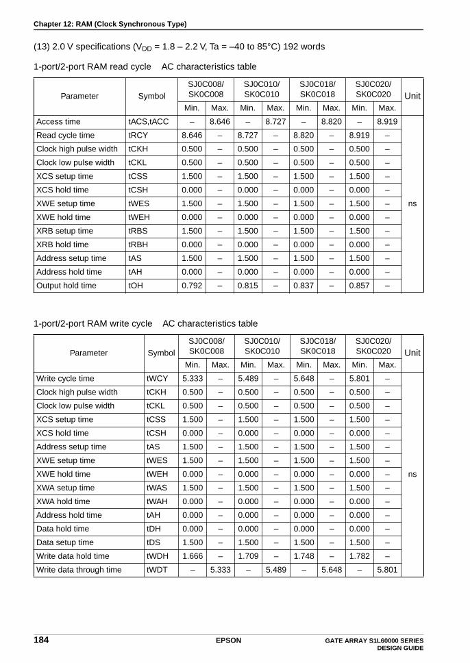
Chapter 12: RAM (Clock Synchronous Type)
(13) 2.0 V specifications (VDD = 1.8 – 2.2 V, Ta = –40 to 85°C) 192 words
1-port/2-port RAM read cycle AC characteristics table
1-port/2-port RAM write cycle AC characteristics table
Parameter SymbolSJ0C008/SK0C008
SJ0C010/SK0C010
SJ0C018/SK0C018
SJ0C020/SK0C020 Unit
Min. Max. Min. Max. Min. Max. Min. Max.
Access time tACS,tACC – 8.646 – 8.727 – 8.820 – 8.919
ns
Read cycle time tRCY 8.646 – 8.727 – 8.820 – 8.919 –
Clock high pulse width tCKH 0.500 – 0.500 – 0.500 – 0.500 –
Clock low pulse width tCKL 0.500 – 0.500 – 0.500 – 0.500 –
XCS setup time tCSS 1.500 – 1.500 – 1.500 – 1.500 –
XCS hold time tCSH 0.000 – 0.000 – 0.000 – 0.000 –
XWE setup time tWES 1.500 – 1.500 – 1.500 – 1.500 –
XWE hold time tWEH 0.000 – 0.000 – 0.000 – 0.000 –
XRB setup time tRBS 1.500 – 1.500 – 1.500 – 1.500 –
XRB hold time tRBH 0.000 – 0.000 – 0.000 – 0.000 –
Address setup time tAS 1.500 – 1.500 – 1.500 – 1.500 –
Address hold time tAH 0.000 – 0.000 – 0.000 – 0.000 –
Output hold time tOH 0.792 – 0.815 – 0.837 – 0.857 –
Parameter SymbolSJ0C008/SK0C008
SJ0C010/SK0C010
SJ0C018/SK0C018
SJ0C020/SK0C020 Unit
Min. Max. Min. Max. Min. Max. Min. Max.
Write cycle time tWCY 5.333 – 5.489 – 5.648 – 5.801 –
ns
Clock high pulse width tCKH 0.500 – 0.500 – 0.500 – 0.500 –
Clock low pulse width tCKL 0.500 – 0.500 – 0.500 – 0.500 –
XCS setup time tCSS 1.500 – 1.500 – 1.500 – 1.500 –
XCS hold time tCSH 0.000 – 0.000 – 0.000 – 0.000 –
Address setup time tAS 1.500 – 1.500 – 1.500 – 1.500 –
XWE setup time tWES 1.500 – 1.500 – 1.500 – 1.500 –
XWE hold time tWEH 0.000 – 0.000 – 0.000 – 0.000 –
XWA setup time tWAS 1.500 – 1.500 – 1.500 – 1.500 –
XWA hold time tWAH 0.000 – 0.000 – 0.000 – 0.000 –
Address hold time tAH 0.000 – 0.000 – 0.000 – 0.000 –
Data hold time tDH 0.000 – 0.000 – 0.000 – 0.000 –
Data setup time tDS 1.500 – 1.500 – 1.500 – 1.500 –
Write data hold time tWDH 1.666 – 1.709 – 1.748 – 1.782 –
Write data through time tWDT – 5.333 – 5.489 – 5.648 – 5.801
184 EPSON GATE ARRAY S1L60000 SERIES DESIGN GUIDE
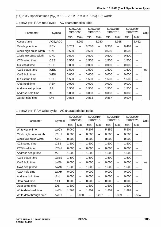
Chapter 12: RAM (Clock Synchronous Type)
(14) 2.0 V specifications (VDD = 1.8 – 2.2 V, Ta = 0 to 70°C) 192 words
1-port/2-port RAM read cycle AC characteristics table
1-port/2-port RAM write cycle AC characteristics table
Parameter SymbolSJ0C008/SK0C008
SJ0C010/SK0C010
SJ0C018/SK0C018
SJ0C020/SK0C020 Unit
Min. Max. Min. Max. Min. Max. Min. Max.
Access time tACS,tACC – 8.203 – 8.280 – 8.368 – 8.462
ns
Read cycle time tRCY 8.203 – 8.280 – 8.368 – 8.462 –
Clock high pulse width tCKH 0.500 – 0.500 – 0.500 – 0.500 –
Clock low pulse width tCKL 0.500 – 0.500 – 0.500 – 0.500 –
XCS setup time tCSS 1.500 – 1.500 – 1.500 – 1.500 –
XCS hold time tCSH 0.000 – 0.000 – 0.000 – 0.000 –
XWE setup time tWES 1.500 – 1.500 – 1.500 – 1.500 –
XWE hold time tWEH 0.000 – 0.000 – 0.000 – 0.000 –
XRB setup time tRBS 1.500 – 1.500 – 1.500 – 1.500 –
XRB hold time tRBH 0.000 – 0.000 – 0.000 – 0.000 –
Address setup time tAS 1.500 – 1.500 – 1.500 – 1.500 –
Address hold time tAH 0.000 – 0.000 – 0.000 – 0.000 –
Output hold time tOH 0.838 – 0.863 – 0.887 – 0.907 –
Parameter SymbolSJ0C008/SK0C008
SJ0C010/SK0C010
SJ0C018/SK0C018
SJ0C020/SK0C020 Unit
Min. Max. Min. Max. Min. Max. Min. Max.
Write cycle time tWCY 5.060 – 5.207 – 5.359 – 5.504 –
ns
Clock high pulse width tCKH 0.500 – 0.500 – 0.500 – 0.500 –
Clock low pulse width tCKL 0.500 – 0.500 – 0.500 – 0.500 –
XCS setup time tCSS 1.500 – 1.500 – 1.500 – 1.500 –
XCS hold time tCSH 0.000 – 0.000 – 0.000 – 0.000 –
Address setup time tAS 1.500 – 1.500 – 1.500 – 1.500 –
XWE setup time tWES 1.500 – 1.500 – 1.500 – 1.500 –
XWE hold time tWEH 0.000 – 0.000 – 0.000 – 0.000 –
XWA setup time tWAS 1.500 – 1.500 – 1.500 – 1.500 –
XWA hold time tWAH 0.000 – 0.000 – 0.000 – 0.000 –
Address hold time tAH 0.000 – 0.000 – 0.000 – 0.000 –
Data hold time tDH 0.000 – 0.000 – 0.000 – 0.000 –
Data setup time tDS 1.500 – 1.500 – 1.500 – 1.500 –
Write data hold time tWDH 1.764 – 1.809 – 1.851 – 1.887 –
Write data through time tWDT – 5.060 – 5.207 – 5.359 – 5.504
GATE ARRAY S1L60000 SERIES EPSON 185DESIGN GUIDE

Chapter 12: RAM (Clock Synchronous Type)
(15) 2.0 V specifications (VDD = 1.8 – 2.2 V, Ta = –40 to 85°C) 256 words
1-port/2-port RAM read cycle AC characteristics table
1-port/2-port RAM write cycle AC characteristics table
Parameter SymbolSJ10008/SK10008
SJ10010/SK10010
SJ10018/SK10018
SJ10020/SK10020 Unit
Min. Max. Min. Max. Min. Max. Min. Max.
Access time tACS,tACC – 9.967 –10.06
4–
10.156
–10.25
6
ns
Read cycle time tRCY 9.967 –10.06
4–
10.156
–10.25
6–
Clock high pulse width tCKH 0.500 – 0.500 – 0.500 – 0.500 –
Clock low pulse width tCKL 0.500 – 0.500 – 0.500 – 0.500 –
XCS setup time tCSS 1.500 – 1.500 – 1.500 – 1.500 –
XCS hold time tCSH 0.000 – 0.000 – 0.000 – 0.000 –
XWE setup time tWES 1.500 – 1.500 – 1.500 – 1.500 –
XWE hold time tWEH 0.000 – 0.000 – 0.000 – 0.000 –
XRB setup time tRBS 1.500 – 1.500 – 1.500 – 1.500 –
XRB hold time tRBH 0.000 – 0.000 – 0.000 – 0.000 –
Address setup time tAS 1.500 – 1.500 – 1.500 – 1.500 –
Address hold time tAH 0.000 – 0.000 – 0.000 – 0.000 –
Output hold time tOH 0.792 – 0.815 – 0.837 – 0.857 –
Parameter SymbolSJ10008/SK10008
SJ10010/SK10010
SJ10018/SK10018
SJ10020/SK10020 Unit
Min. Max. Min. Max. Min. Max. Min. Max.
Write cycle time tWCY 5.398 – 5.551 – 5.697 – 5.859 –
ns
Clock high pulse width tCKH 0.500 – 0.500 – 0.500 – 0.500 –
Clock low pulse width tCKL 0.500 – 0.500 – 0.500 – 0.500 –
XCS setup time tCSS 1.500 – 1.500 – 1.500 – 1.500 –
XCS hold time tCSH 0.000 – 0.000 – 0.000 – 0.000 –
Address setup time tAS 1.500 – 1.500 – 1.500 – 1.500 –
XWE setup time tWES 1.500 – 1.500 – 1.500 – 1.500 –
XWE hold time tWEH 0.000 – 0.000 – 0.000 – 0.000 –
XWA setup time tWAS 1.500 – 1.500 – 1.500 – 1.500 –
XWA hold time tWAH 0.000 – 0.000 – 0.000 – 0.000 –
Address hold time tAH 0.000 – 0.000 – 0.000 – 0.000 –
Data hold time tDH 0.000 – 0.000 – 0.000 – 0.000 –
Data setup time tDS 1.500 – 1.500 – 1.500 – 1.500 –
Write data hold time tWDH 1.698 – 1.738 – 1.777 – 1.811 –
Write data through time tWDT – 5.398 – 5.551 – 5.697 – 5.859
186 EPSON GATE ARRAY S1L60000 SERIES DESIGN GUIDE
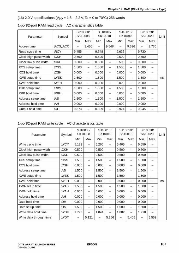
Chapter 12: RAM (Clock Synchronous Type)
(16) 2.0 V specifications (VDD = 1.8 – 2.2 V, Ta = 0 to 70°C) 256 words
1-port/2-port RAM read cycle AC characteristics table
1-port/2-port RAM write cycle AC characteristics table
Parameter SymbolSJ10008/SK10008
SJ10010/SK10010
SJ10018/SK10018
SJ10020/SK10020 Unit
Min. Max. Min. Max. Min. Max. Min. Max.
Access time tACS,tACC – 9.455 – 9.548 – 9.636 – 9.730
ns
Read cycle time tRCY 9.455 – 9.548 – 9.636 – 9.730 –
Clock high pulse width tCKH 0.500 – 0.500 – 0.500 – 0.500 –
Clock low pulse width tCKL 0.500 – 0.500 – 0.500 – 0.500 –
XCS setup time tCSS 1.500 – 1.500 – 1.500 – 1.500 –
XCS hold time tCSH 0.000 – 0.000 – 0.000 – 0.000 –
XWE setup time tWES 1.500 – 1.500 – 1.500 – 1.500 –
XWE hold time tWEH 0.000 – 0.000 – 0.000 – 0.000 –
XRB setup time tRBS 1.500 – 1.500 – 1.500 – 1.500 –
XRB hold time tRBH 0.000 – 0.000 – 0.000 – 0.000 –
Address setup time tAS 1.500 – 1.500 – 1.500 – 1.500 –
Address hold time tAH 0.000 – 0.000 – 0.000 – 0.000 –
Output hold time tOH 0.873 – 0.899 – 0.924 – 0.945 –
Parameter SymbolSJ10008/SK10008
SJ10010/SK10010
SJ10018/SK10018
SJ10020/SK10020 Unit
Min. Max. Min. Max. Min. Max. Min. Max.
Write cycle time tWCY 5.121 – 5.266 – 5.405 – 5.559 –
ns
Clock high pulse width tCKH 0.500 – 0.500 – 0.500 – 0.500 –
Clock low pulse width tCKL 0.500 – 0.500 – 0.500 – 0.500 –
XCS setup time tCSS 1.500 – 1.500 – 1.500 – 1.500 –
XCS hold time tCSH 0.000 – 0.000 – 0.000 – 0.000 –
Address setup time tAS 1.500 – 1.500 – 1.500 – 1.500 –
XWE setup time tWES 1.500 – 1.500 – 1.500 – 1.500 –
XWE hold time tWEH 0.000 – 0.000 – 0.000 – 0.000 –
XWA setup time tWAS 1.500 – 1.500 – 1.500 – 1.500 –
XWA hold time tWAH 0.000 – 0.000 – 0.000 – 0.000 –
Address hold time tAH 0.000 – 0.000 – 0.000 – 0.000 –
Data hold time tDH 0.000 – 0.000 – 0.000 – 0.000 –
Data setup time tDS 1.500 – 1.500 – 1.500 – 1.500 –
Write data hold time tWDH 1.798 – 1.841 – 1.882 – 1.918 –
Write data through time tWDT – 5.121 – 5.266 – 5.405 – 5.559
GATE ARRAY S1L60000 SERIES EPSON 187DESIGN GUIDE
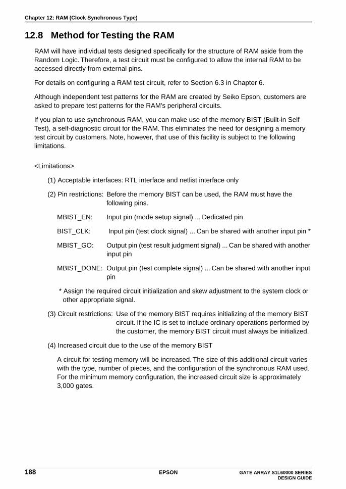
Chapter 12: RAM (Clock Synchronous Type)
12.8 Method for Testing the RAM
RAM will have individual tests designed specifically for the structure of RAM aside from the Random Logic. Therefore, a test circuit must be configured to allow the internal RAM to be accessed directly from external pins.
For details on configuring a RAM test circuit, refer to Section 6.3 in Chapter 6.
Although independent test patterns for the RAM are created by Seiko Epson, customers are asked to prepare test patterns for the RAM's peripheral circuits.
If you plan to use synchronous RAM, you can make use of the memory BIST (Built-in Self Test), a self-diagnostic circuit for the RAM. This eliminates the need for designing a memory test circuit by customers. Note, however, that use of this facility is subject to the following limitations.
<Limitations>
(1) Acceptable interfaces: RTL interface and netlist interface only
(2) Pin restrictions: Before the memory BIST can be used, the RAM must have the following pins.
MBIST_EN: Input pin (mode setup signal) ... Dedicated pin
BIST_CLK: Input pin (test clock signal) ... Can be shared with another input pin *
MBIST_GO: Output pin (test result judgment signal) ... Can be shared with another input pin
MBIST_DONE: Output pin (test complete signal) ... Can be shared with another input pin
* Assign the required circuit initialization and skew adjustment to the system clock or other appropriate signal.
(3) Circuit restrictions: Use of the memory BIST requires initializing of the memory BIST circuit. If the IC is set to include ordinary operations performed by the customer, the memory BIST circuit must always be initialized.
(4) Increased circuit due to the use of the memory BIST
A circuit for testing memory will be increased. The size of this additional circuit varies with the type, number of pieces, and the configuration of the synchronous RAM used. For the minimum memory configuration, the increased circuit size is approximately 3,000 gates.
188 EPSON GATE ARRAY S1L60000 SERIES DESIGN GUIDE
Chapter 12: RAM (Clock Synchronous Type)
<Schematic diagram of the memory BIST>
When using the memory BIST, there are some usage precautions and other information that the customer needs to confirm before use. Please contact Seiko Epson or its distributor.
12.9 Estimating RAM Current Consumption
(1) 1-port RAM
• When operating with VDD = 2.5 V
–5 x 10⁻⁵ x number of words2 + 0.0499 x number of words + 8.8607 + (0.007 x number of words + 1.2262) x number of bits [µA/MHz)]
• When operating with VDD = 2.0 V
–4 x 10⁻⁵ x number of words2 + 0.0391 x number of words + 6.3679 + (0.007 x number of words + 1.2262) x number of bits [µA/MHz)]
(2) 2-port RAM
• When operating with VDD = 2.5 V
–1 x 10⁻⁴ x number of words2 + 0.0998 x number of words + 17.7358 + (0.172 x number of words + 3.273) x number of bits [µA/MHz)]
• When operating with VDD = 2.0 V
–8 x 10⁻⁵ x number of words2 + 0.0782 x number of words + 12.7358 + (0.014 x number of words + 2.4524) x number of bits [µA/MHz)]
Addr
Data
Controller
RAM
BIST_CLK (SYS_CLK)
BIST_CLKBIST_EN
BIST_EN
MBIST_ENMBIST_CK
T_Dn
T_Am
CK
Dn
Am Am
Dn
RW
CK
Yn YnYn
MBIST_GO_,DONEMBIST_GO_,DONE
GATE ARRAY S1L60000 SERIES EPSON 189DESIGN GUIDE

Appendix: A1. Electrical Characteristica Data
Appendix A1. Electrical Characteristica Data
A1.1 3.3V operation
Output current characteristics (3.3V±0.3V)
The alphanumerics of the TYPE∗ (S, M, 1-4) indicate the output cell names (xx ∗ x).
Example: HOB3T Indicates TYPE3.
Table A1-1
TYPE numberOutput current
IOH (mA) IOL (mA)
TYPE S -0.1 0.1
TYPE M -1 1
TYPE 1 -3 3
TYPE 2 -6 6
TYPE 3 -12 12
TYPE 4 -24 24
PCI Confirmed to the PCI standard
190 EPSON GATE ARRAY S1L60000 SERIES DESIGN GUIDE

Appendix: A1. Electrical Characteristica Data
Input Buffer Characteristics (3.3V±0.3V)
• Standard type
• Schmitt-Trigger cell
Figure A1-1 Input buffer characteristics(LVTTL level)
Figure A1-2 Input buffer characteristics (CMOS level)
Figure A1-3 Input buffer characteristics(3V PCI)
Figure A1-4 Input buffer characteristics(LVTTL level)
Figure A1-5 Input buffer characteristics (CMOS level )
4
3
2
1
1 2 3 4VIN (V)
VO
UT (
V)
0
HVDD = 3.0V
Ta = 25°C
HVDD = 3.6V
HVDD = 3.3V
4
3
2
1
1 2 3 4VIN (V)
VO
UT (
V)
0
HVDD = 3.0V
Ta = 25°C
HVDD = 3.6V
HVDD = 3.3V
4
3
2
1
1 2 3 4VIN (V)
VO
UT (
V)
0
HVDD = 3.0V
Ta = 25°C
HVDD = 3.6V
HVDD = 3.3V
4
3
2
1
1 2 3 4VIN (V)
VO
UT (
V)
0
Ta = 25°C
HVDD = 3.6V
HVDD = 3.3V
HVDD = 3.0V
4
3
2
1
1 2 3 4VIN (V)
VO
UT
(V)
0
HVDD = 3.0V
Ta = 25°C
HVDD = 3.6V
HVDD = 3.3V
GATE ARRAY S1L60000 SERIES EPSON 191DESIGN GUIDE
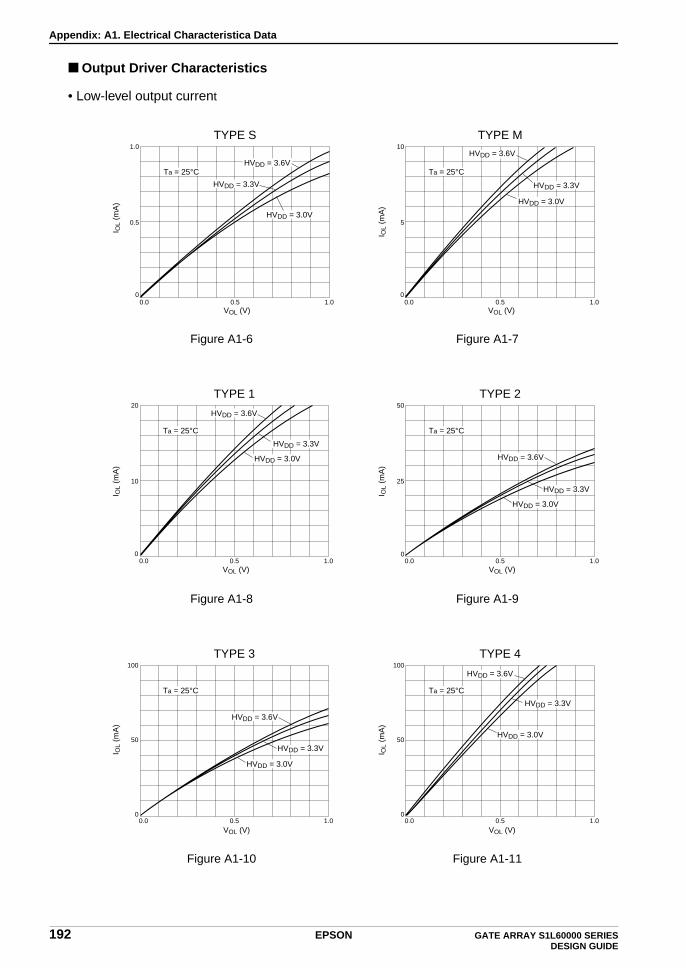
Appendix: A1. Electrical Characteristica Data
Output Driver Characteristics
• Low-level output current
Figure A1-6 Figure A1-7
Figure A1-8 Figure A1-9
Figure A1-10 Figure A1-11
1.0
0.5
Ta = 25°C
1.0
I OL
(mA
)
VOL (V)
TYPE S
0.50.00
HVDD = 3.6V
HVDD = 3.3V
HVDD = 3.0V
10
5
Ta = 25°C
1.0
I OL
(mA
)
VOL (V)
TYPE M
0.50.00
HVDD = 3.6V
HVDD = 3.3V
HVDD = 3.0V
20
10
Ta = 25°C
1.0
I OL
(mA
)
VOL (V)
TYPE 1
0.50.00
HVDD = 3.6V
HVDD = 3.3V
HVDD = 3.0V
50
25
Ta = 25°C
1.0
I OL
(mA
)
VOL (V)
TYPE 2
0.50.00
HVDD = 3.6V
HVDD = 3.3V
HVDD = 3.0V
100
50
Ta = 25°C
1.0
I OL
(mA
)
VOL (V)
TYPE 3
0.50.00
HVDD = 3.6V
HVDD = 3.3V
HVDD = 3.0V
100
50
Ta = 25°C
1.0
I OL
(mA
)
VOL (V)
TYPE 4
0.50.00
HVDD = 3.6V
HVDD = 3.3V
HVDD = 3.0V
192 EPSON GATE ARRAY S1L60000 SERIES DESIGN GUIDE

Appendix: A1. Electrical Characteristica Data
• High-level output current
Figure A1-12 Figure A1-13
Output voltage VOH – Supply voltage HVDD (V)
Figure A1-14
Output voltage VOH – Supply voltage HVDD (V)
Figure A1-15
Output voltage VOH – Supply voltage HVDD (V)
Figure A1-16
Output voltage VOH – Supply voltage HVDD (V)
Figure A1-17
100
50
Ta = 25°C
1.0
I OL
(mA
)
VOL (V)
PCI 3V
0.50.00
HVDD = 3.6V
HVDD = 3.3V
HVDD = 3.0V
100
50
Ta = 25°C
1.0
I OL
(mA
)
VOL (V)
TYPE 1 to 4
0.50.00
HVDD = 3.3VTYPE 4
TYPE 3
TYPE 2
TYPE 1
I OH
(m
A)
-1.0
-0.5
0.0
Ta = 25°C
-1.0
TYPE S
-0.5
HVDD = 3.6V
HVDD = 3.3V
HVDD = 3.0V I OH
(m
A)
-1.0
-0.5
0.0
Ta = 25°C
-1.0
TYPE M
-0.5
HVDD = 3.6V
HVDD = 3.3V
HVDD = 3.0V
I OH
(m
A)
-20
-10
0
Ta = 25°C
-1.0
TYPE 1
-0.50.0
HVDD = 3.6V
HVDD = 3.3V
HVDD = 3.0V
I OH
(m
A)
-50
-25
0
Ta = 25°C
-1.0
TYPE 2
-0.50.0
HVDD = 3.6V
HVDD = 3.3V
HVDD = 3.0V
GATE ARRAY S1L60000 SERIES EPSON 193DESIGN GUIDE
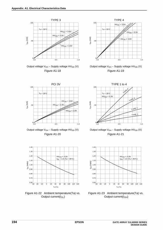
Appendix: A1. Electrical Characteristica Data
Output voltage VOH – Supply voltage HVDD (V)
Figure A1-18
Output voltage VOH – Supply voltage HVDD (V)
Figure A1-19
Output voltage VOH – Supply voltage HVDD (V)
Figure A1-20
Output voltage VOH – Supply voltage HVDD (V)
Figure A1-21
Figure A1-22 Ambient temperature(Ta) vs. Output current(IOL)
Figure A1-23 Ambient temperature(Ta) vs. Output current(IOH)
I OH
(m
A)
-100
-50
0
Ta = 25°C
-1.0
TYPE 3
-0.50.0
HVDD = 3.6V
HVDD = 3.3V
HVDD = 3.0V
I OH
(m
A)
-100
-50
0
Ta = 25°C
-1.0
TYPE 4
-0.50.0
HVDD = 3.6V
HVDD = 3.3V
HVDD = 3.0V
I OH
(m
A)
-100
-50
0
Ta = 25°C
-1.0
PCI 3V
-0.50.0
HVDD = 3.6V
HVDD = 3.3V
HVDD = 3.0V
I OH
(m
A)
-100
-50
0
Ta = 25°C
-1.0
TYPE 1 to 4
-0.50.0
HVDD = 3.3V
TYPE 4
TYPE 3
TYPE 2
TYPE 1
1.40
1.30
1.20
1.10
1.00
0.90
0.80
0.70
0.60
I OL
(rat
io)
-40 -20-60 200 40
Ta (°C)
60 80 100 120 140
HVDD = 3.3VIOL = 1.0 (Ta = 25°C)
1.40
1.30
1.20
1.10
1.00
0.90
0.80
0.70
0.60
I OH
(rat
io)
-40 -20-60 200 40
Ta (°C)
60 80 100 120 140
HVDD = 3.3VIOH = 1.0 (Ta = 25°C)
194 EPSON GATE ARRAY S1L60000 SERIES DESIGN GUIDE

Appendix: A1. Electrical Characteristica Data
Output Delay Time vs. Output Load Capacitance(CL)
Figure A1-24 Output Delay Time(tPLH) vs.Output load capacitance(CL)
Figure A1-25 Output Delay Time(tPHL) vs.Output load capacitance(CL)
Figure A1-26 Output Delay Time(tPLH) vs.Output load capacitance(CL)
Figure A1-27 Output Delay Time(tPHL) vs.Output load capacitance(CL)
Figure A1-28 Output Delay Time(tPLH) vs.Output load capacitance(CL)
Figure A1-29 Output Delay Time(tPHL) vs.Output load capacitance(CL)
0
400
300
200
100
050 100 150 200
HOBST
HOBMT
HVDD = 3.3VVth = 1.65VTa = 25°C
CL (pF)
t
(ns
)P
HL
0
400
300
200
100
0
CL (pF)50 100 150 200
HOBST
HOBMT
HVDD = 3.3VVth = 1.65VTa = 25°C
t
(ns
)P
HL
0
20
15
10
5
0
CL (pF)50 100 150 200
HOB1T
HOB2THOB3AT
HOB4AT
HVDD = 3.3VVth = 1.65VTa = 25°C
t
(ns
)P
HL
0
20
15
10
5
0
CL (pF)50 100 150 200
HOB1T
HOB2T
HOB3AT
HOB4AT
HVDD = 3.3VVth = 1.65VTa = 25°C
t
(ns
)P
HL
0
5
4
3
2
1
0
CL (pF)
t
(ns
)
50 100 150 200
HOBPBT
HVDD = 3.3VVth = 1.65VTa = 25°C
PH
L
0
5
4
3
2
1
0
CL (pF)
t
(ns
)
50 100 150 200
HOBPBT
HVDD = 3.3VVth = 1.65VTa = 25°C
PH
L
GATE ARRAY S1L60000 SERIES EPSON 195DESIGN GUIDE

Appendix: A1. Electrical Characteristica Data
Output Delay Time vs. CL
Figure A1-30 Rising Time (tr) vs.Output load capacitance (CL)
Figure A1-31 Falling Time (tf) vs.Output load capacitance (CL)
Figure A1-32 Rising Time (tr) vs.Output load capacitance (CL)
Figure A1-33 Falling Time (tf) vs.Output load capacitance (CL)
Figure A1-34 Rising Time (tr) vs.Output load capacitance (CL)
Figure A1-35 Falling Time (tf) vs.Output load capacitance (CL)
0
800
600
400
200
0
CL (pF)
t
(
ns)
50 100 150 200
HOBST
HOBMT
HVDD = 3.3VTa = 25°C
r (1
0%-9
0%)
0
800
600
400
200
0
CL (pF)
t
(
ns)
50 100 150 200
HOBST
HOBMT
HVDD = 3.3VTa = 25°C
f (10
%-9
0%)
0
40
30
20
10
0
CL (pF)
t
(
ns)
50 100 150 200
HOB1T
HOB2T
HOB3AT
HOB4AT
HVDD = 3.3VTa = 25°C
r (1
0%-9
0%)
0
40
30
20
10
0
CL (pF)
t
(n
s)
50 100 150 200
HOB1T
HOB2T
HOB3AT
HOB4AT
HVDD = 3.3VTa = 25°C
f (10
%-9
0%)
0
10
8
6
4
2
0
CL (pF)50 100 150 200
HOBPBT
HVDD = 3.3VTa = 25°C
t
(
ns)
r (1
0%-9
0%)
0
10
8
6
4
2
0
CL (pF)50 100 150 200
HOBPBT
HVDD = 3.3VTa = 25°C
t
(
ns)
f (10
%-9
0%)
196 EPSON GATE ARRAY S1L60000 SERIES DESIGN GUIDE

Appendix: A1. Electrical Characteristica Data
Pull-Up and Pull-Down Resistance
• Pull-Up characteristics
• Pull-Down characteristics
Figure A1-36 RPLU vs. HVDD characteristics Figure A1-37 RPLU vs. Ta characteristics
Figure A1-38 RPLD vs. HVDD characteristics Figure A1-39 RPLD vs. Ta characteristics
2.4
HVDD (V)
RP
LU (k
Ω)
2.7 3 3.3 3.6 3.9 4.2
Ta = 25°C
TYPE 1
TYPE 2
250
200
150
100
50
0-60 -40 -20 0 20 40 60 80 100 120 140
RP
LU (k
Ω)
TYPE 1
TYPE 2
250
200
150
100
50
0
HVDD = 3.3V
Ta (°C)
2.4
HVDD (V)
RP
LD (k
Ω)
2.7 3 3.3 3.6 3.9 4.2
Ta = 25°C
TYPE 1
TYPE 2
250
200
150
100
50
0-60 -40 -20 0 20 40 60 80 100 120 140
Ta (°C)
RP
LD (k
Ω)
TYPE 1
TYPE 2
250
200
150
100
50
0
HVDD = 3.3V
GATE ARRAY S1L60000 SERIES EPSON 197DESIGN GUIDE

Appendix: A1. Electrical Characteristica Data
Output Waveforms
• Output buffer output waveforms: High speed PDV (HOB3AT)
• Output buffer output waveforms: Normal PDV (HOB3T)
• Output buffer output waveforms: Low noise PDV (HOB3BT)
Figure A1-40
Figure A1-41
Figure A1-42
Output buffer Conditions : HVDD = 3.3V, Ta = 25°C, CL = 15pF, IOL = 12mA
6
4
2
0
-2
Out
put v
olta
ge
Vo
(V)
(5ns/div)
Output buffer Conditions : HVDD = 3.3V, Ta = 25°C, CL= 15pF, IOL = 12mA
6
4
2
0
-2
Out
put v
olta
ge
Vo
(V)
(5ns/div)
Outpdut buffer Conditions : HVDD = 3.3V, Ta = 25°C, CL = 15pF, IOL = 12mA
6
4
2
0
-2
Out
put v
olta
ge
Vo
(V)
(5ns/div)
198 EPSON GATE ARRAY S1L60000 SERIES DESIGN GUIDE

Appendix: A1. Electrical Characteristica Data
A1.2 2.5V operation
Output current characteristics (2.5V±0.2V)
The alphanumerics of the TYPE∗ (S, M, 1-4) indicate the output cell names (xx ∗ x).
Example: OB3T Indicates TYPE3.
Table A1-2
TYPE numberOutput current
IOH (mA) IOL (mA)
TYPE S -0.1 0.1
TYPE M -1 1
TYPE 1 -3 3
TYPE 2 -6 6
TYPE 3 -9 9
TYPE 4 -18 18
GATE ARRAY S1L60000 SERIES EPSON 199DESIGN GUIDE

Appendix: A1. Electrical Characteristica Data
Input Buffer Characteristics (2.5V±0.2V)
• Standard type
• Schmitt-Trigger cell
Figure A1-43 Input buffer characteristics(CMOS level)
Figure A1-44 Input buffer characteristics(CMOS leveI)
4
3
2
1
1 2 3 4VIN (V)
VO
UT (
V)
0
Ta = 25°C
VDD = 2.7V
VDD = 2.5V
VDD = 2.3V
4
3
2
1
1 2 3 4VIN (V)
VO
UT (
V)
0
Ta = 25°C
VDD = 2.7V
VDD = 2.5V
VDD = 2.3V
200 EPSON GATE ARRAY S1L60000 SERIES DESIGN GUIDE
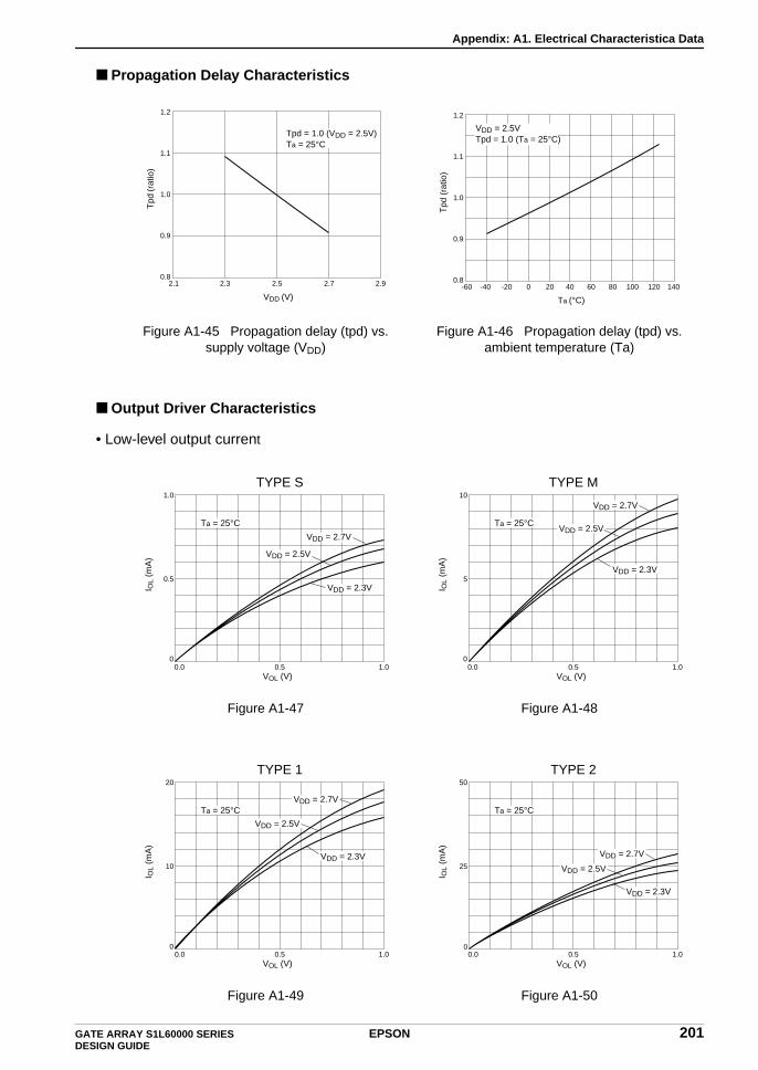
Appendix: A1. Electrical Characteristica Data
Propagation Delay Characteristics
Output Driver Characteristics
• Low-level output current
Figure A1-45 Propagation delay (tpd) vs.supply voltage (VDD)
Figure A1-46 Propagation delay (tpd) vs.ambient temperature (Ta)
Figure A1-47 Figure A1-48
Figure A1-49 Figure A1-50
1.2
1.1
1.0
0.9
0.8
Tpd
(rat
io)
2.1
VDD (V)
2.3 2.5 2.7 2.9
Tpd = 1.0 (VDD = 2.5V)Ta = 25°C
1.2
1.1
1.0
0.9
0.8
Tpd
(ra
tio)
-40 -20-60 200 40
Ta (°C)
60 80 100 120 140
VDD = 2.5VTpd = 1.0 (Ta = 25°C)I O
L (m
A)
1.0
0.5
Ta = 25°C
1.0VOL (V)
TYPE S
0.50.00
VDD = 2.7V
VDD = 2.5V
VDD = 2.3V I OL
(mA
)
10
5
Ta = 25°C
1.0VOL (V)
TYPE M
0.50.00
VDD = 2.7V
VDD = 2.5V
VDD = 2.3V
I OL
(mA
)
20
10
Ta = 25°C
1.0VOL (V)
TYPE 1
0.50.00
VDD = 2.7V
VDD = 2.5V
VDD = 2.3V
I OL
(mA
)
50
25
Ta = 25°C
1.0VOL (V)
TYPE 2
0.50.00
VDD = 2.7V
VDD = 2.5V
VDD = 2.3V
GATE ARRAY S1L60000 SERIES EPSON 201DESIGN GUIDE
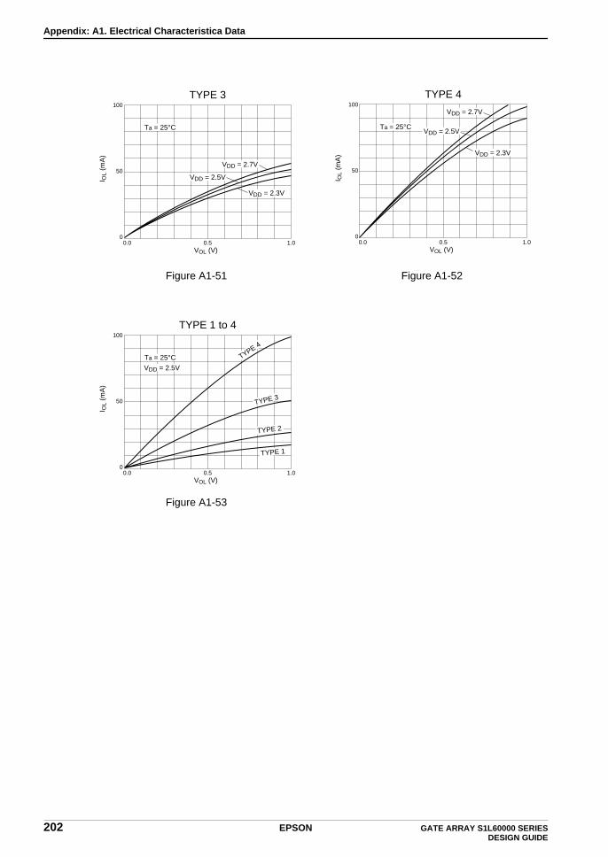
Appendix: A1. Electrical Characteristica Data
Figure A1-51 Figure A1-52
Figure A1-53
I OL
(mA
)100
50
Ta = 25°C
1.0VOL (V)
TYPE 3
0.50.00
VDD = 2.7V
VDD = 2.5V
VDD = 2.3V
I OL
(mA
)
100
50
Ta = 25°C
1.0VOL (V)
TYPE 4
0.50.00
VDD = 2.7V
VDD = 2.5V
VDD = 2.3V
I OL
(mA
)
100
50
Ta = 25°C
1.0VOL (V)
TYPE 1 to 4
0.50.00
VDD = 2.5V
TYPE 4
TYPE 3
TYPE 2
TYPE 1
202 EPSON GATE ARRAY S1L60000 SERIES DESIGN GUIDE

Appendix: A1. Electrical Characteristica Data
• High-level output current
Output voltage VOH – Supply voltage VDD (V)
Figure A1-54
Output voltage VOH – Supply voltage VDD (V)
Figure A1-55
Output voltage VOH – Supply voltage VDD (V)
Figure A1-56
Output voltage VOH – Supply voltage VDD (V)
Figure A1-57
Output voltage VOH – Supply voltage VDD (V)
Figure A1-58
Output voltage VOH – Supply voltage VDD (V)
Figure A1-59
I OH
(m
A)
-1.0
-0.5
0.0
Ta = 25°C
-1.0
TYPE S
-0.5
VDD = 2.7V
VDD = 2.5V
VDD = 2.3V
I OH
(m
A)
-10
-5
0.0
Ta = 25°C
-1.0
TYPE M
-0.5
VDD = 2.7V
VDD = 2.5V
VDD = 2.3V
I OH
(m
A)
-20
-10
0
Ta = 25°C
-1.0
TYPE 1
-0.50.0
VDD = 2.7V
VDD = 2.5V
VDD = 2.3V I OH
(m
A)
-50
-25
0
Ta = 25°C
-1.0
TYPE 2
-0.50.0
VDD = 2.7V
VDD = 2.5V
VDD = 2.3V
I OH
(m
A)
-100
-50
0
Ta = 25°C
-1.0
TYPE 3
-0.50.0
VDD = 2.7V
VDD = 2.5V
VDD = 2.3V
I OH
(m
A)
-100
-50
0
Ta = 25°C
-1.0
TYPE 4
-0.50.0
VDD = 2.7V
VDD = 2.5V
VDD = 2.3V
GATE ARRAY S1L60000 SERIES EPSON 203DESIGN GUIDE
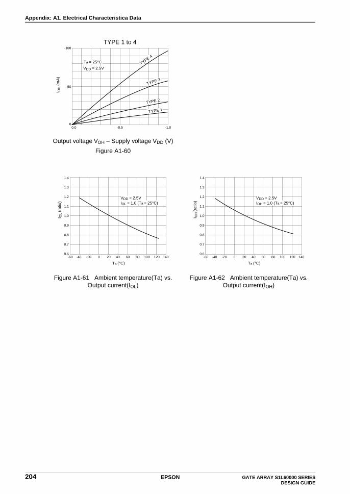
Appendix: A1. Electrical Characteristica Data
Output voltage VOH – Supply voltage VDD (V)
Figure A1-60
Figure A1-61 Ambient temperature(Ta) vs.Output current(IOL)
Figure A1-62 Ambient temperature(Ta) vs.Output current(IOH)
I OH
(m
A)
-100
-50
0
Ta = 25°C
-1.0
TYPE 1 to 4
-0.50.0
VDD = 2.5VTYPE 4
TYPE 3
TYPE 2
TYPE 1
1.4
1.3
1.2
1.1
1.0
0.9
0.8
0.7
0.6
I OL
(rat
io)
-40 -20-60 200 40
Ta (°C)
60 80 100 120 140
VDD = 2.5VIOL = 1.0 (Ta = 25°C)
1.4
1.3
1.2
1.1
1.0
0.9
0.8
0.7
0.6
I OH
(rat
io)
-40 -20-60 200 40
Ta (°C)
60 80 100 120 140
VDD = 2.5VIOH = 1.0 (Ta = 25°C)
204 EPSON GATE ARRAY S1L60000 SERIES DESIGN GUIDE

Appendix: A1. Electrical Characteristica Data
Output Delay Time vs. Output Load Capacitance (CL)
Figure A1-63 Output Delay Time(tPLH) vs.Output load capacitance(CL)
Figure A1-64 Output Delay Time(tPHL) vs.Output load capacitance(CL)
Figure A1-65 Output Delay Time(tPLH) vs.Output load capacitance(CL)
Figure A1-66 Output Delay Time(tPHL) vs.Output load capacitance(CL)
0
400
300
200
100
0
CL (pF)
t
(ns
)
50 100 150 200
OBST
OBMT
VDD = 2.5VVth = 1.25VTa = 25°C
PLH
0
400
300
200
100
0
CL (pF)
t
(ns
)
50 100 150 200
OBST
OBMT
VDD = 2.5VVth = 1.25VTa = 25°C
PH
L
0
20
15
10
5
0
CL (pF)
t
(ns
)
50 100 150 200
OB1T
OB2TOB3AT
OB4AT
VDD = 2.5VVth = 1.25VTa = 25°C
PLH
0
20
15
10
5
0
CL (pF)
t
(ns
)
50 100 150 200
OB1T
OB2T
OB3AT
OB4AT
VDD = 2.5VVth = 1.25VTa = 25°C
PH
L
GATE ARRAY S1L60000 SERIES EPSON 205DESIGN GUIDE
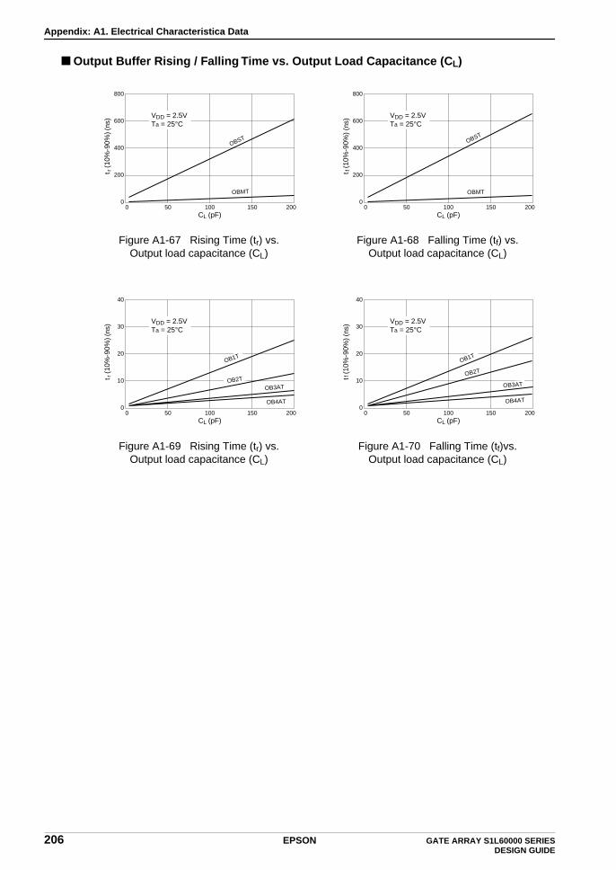
Appendix: A1. Electrical Characteristica Data
Output Buffer Rising / Falling Time vs. Output Load Capacitance (CL)
Figure A1-67 Rising Time (tr) vs.Output load capacitance (CL)
Figure A1-68 Falling Time (tf) vs.Output load capacitance (CL)
Figure A1-69 Rising Time (tr) vs.Output load capacitance (CL)
Figure A1-70 Falling Time (tf)vs. Output load capacitance (CL)
0
800
600
400
200
0
CL (pF)
t
(
ns)
50 100 150 200
OBST
OBMT
VDD = 2.5VTa = 25°C
r (1
0%-9
0%)
0
800
600
400
200
0
CL (pF)
t
(
ns)
50 100 150 200
OBST
OBMT
VDD = 2.5VTa = 25°C
f (10
%-9
0%)
0
40
30
20
10
0
CL (pF)
t
(
ns)
50 100 150 200
OB1T
OB2T
OB3AT
OB4AT
VDD = 2.5VTa = 25°C
r (1
0%-9
0%)
0
40
30
20
10
0
CL (pF)
t
(
ns)
50 100 150 200
OB1T
OB2T
OB3AT
OB4AT
VDD = 2.5VTa = 25°C
f (10
%-9
0%)
206 EPSON GATE ARRAY S1L60000 SERIES DESIGN GUIDE
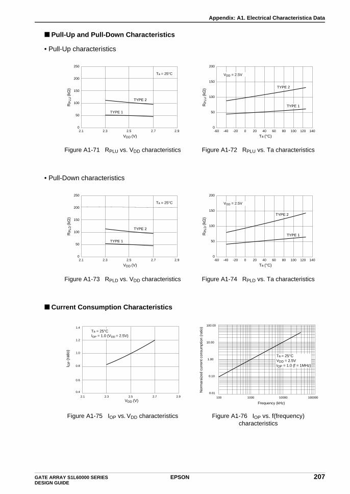
Appendix: A1. Electrical Characteristica Data
Pull-Up and Pull-Down Characteristics
• Pull-Up characteristics
• Pull-Down characteristics
Current Consumption Characteristics
Figure A1-71 RPLU vs. VDD characteristics Figure A1-72 RPLU vs. Ta characteristics
Figure A1-73 RPLD vs. VDD characteristics Figure A1-74 RPLD vs. Ta characteristics
Figure A1-75 IOP vs. VDD characteristics Figure A1-76 IOP vs. f(frequency) characteristics
2.1
VDD (V)
RP
LU (k
Ω)
2.3 2.5 2.7 2.9
Ta = 25°C
TYPE 1
TYPE 2
250
200
150
100
50
0-60 -40 -20 0 20 40 60 80 100 120 140
Ta (°C)
RP
LU (k
Ω)
TYPE 1
TYPE 2
200
150
100
50
0
VDD = 2.5V
2.1
VDD (V)
RP
LD (k
Ω)
2.3 2.5 2.7 2.9
Ta = 25°C
TYPE 1
TYPE 2
250
200
150
100
50
0-60 -40 -20 0 20 40 60 80 100 120 140
Ta (°C)
RP
LD (k
Ω)
TYPE 1
TYPE 2
200
150
100
50
0
VDD = 2.5V
2.1
VDD (V)
I OP (
ratio
)
2.3 2.5 2.7 2.9
1.4
1.2
1.0
0.8
0.6
0.4
Ta = 25°CIOP = 1.0 (VDD = 2.5V)
Nor
mar
aize
d cu
rren
t con
sum
ptio
n (r
atio
)
100 1000
Frequency (kHz)
10000 100000
100.00
10.00
1.00
0.10
0.01
Ta = 25°CVDD = 2.5VIOP = 1.0 (f = 1MHz)
GATE ARRAY S1L60000 SERIES EPSON 207DESIGN GUIDE
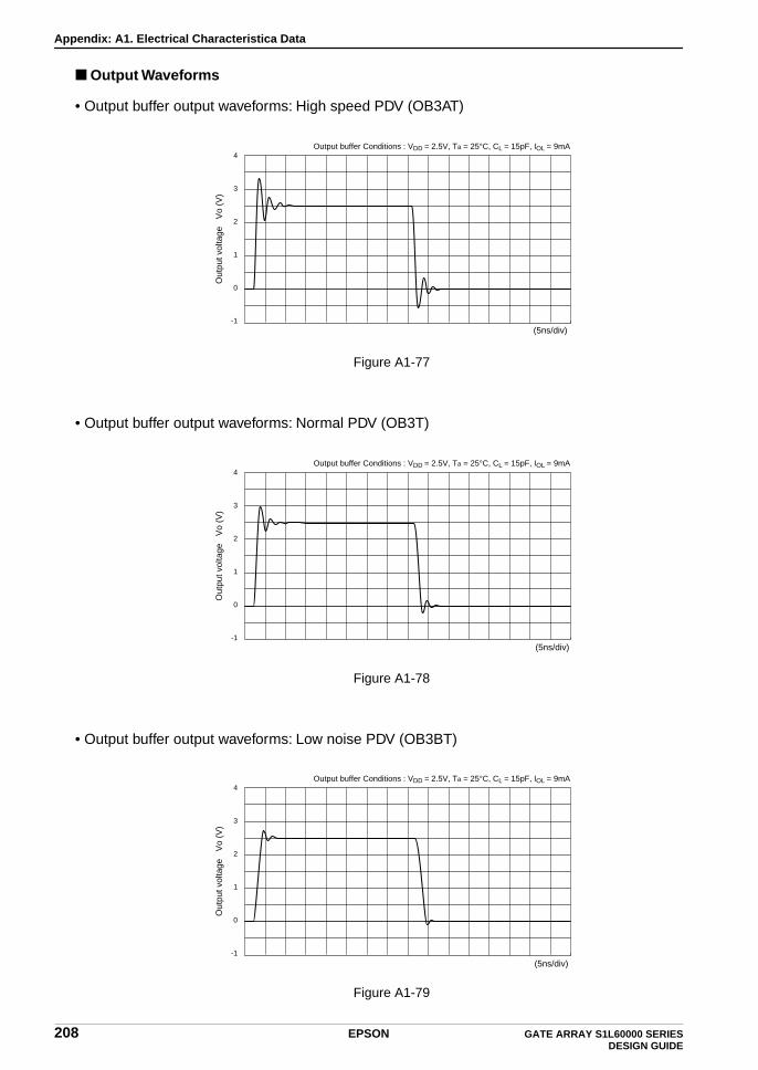
Appendix: A1. Electrical Characteristica Data
Output Waveforms
• Output buffer output waveforms: High speed PDV (OB3AT)
• Output buffer output waveforms: Normal PDV (OB3T)
• Output buffer output waveforms: Low noise PDV (OB3BT)
Figure A1-77
Figure A1-78
Figure A1-79
Output buffer Conditions : VDD = 2.5V, Ta = 25°C, CL = 15pF, IOL = 9mA4
3
2
1
0
-1
Out
put v
olta
ge
Vo
(V)
(5ns/div)
Output buffer Conditions : VDD = 2.5V, Ta = 25°C, CL = 15pF, IOL = 9mA4
3
2
1
0
-1
Out
put v
olta
ge
Vo
(V)
(5ns/div)
Output buffer Conditions : VDD = 2.5V, Ta = 25°C, CL = 15pF, IOL = 9mA4
3
2
1
0
-1
Out
put v
olta
ge
Vo
(V)
(5ns/div)
208 EPSON GATE ARRAY S1L60000 SERIES DESIGN GUIDE
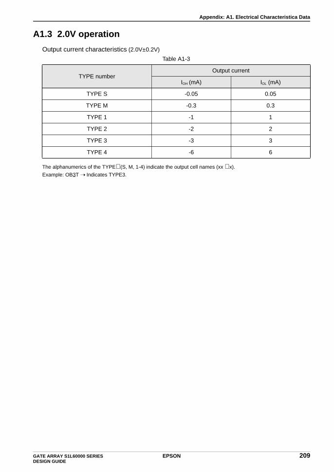
Appendix: A1. Electrical Characteristica Data
A1.3 2.0V operation
Output current characteristics (2.0V±0.2V)
The alphanumerics of the TYPE∗ (S, M, 1-4) indicate the output cell names (xx ∗ x).
Example: OB3T Indicates TYPE3.
Table A1-3
TYPE numberOutput current
IOH (mA) IOL (mA)
TYPE S -0.05 0.05
TYPE M -0.3 0.3
TYPE 1 -1 1
TYPE 2 -2 2
TYPE 3 -3 3
TYPE 4 -6 6
GATE ARRAY S1L60000 SERIES EPSON 209DESIGN GUIDE
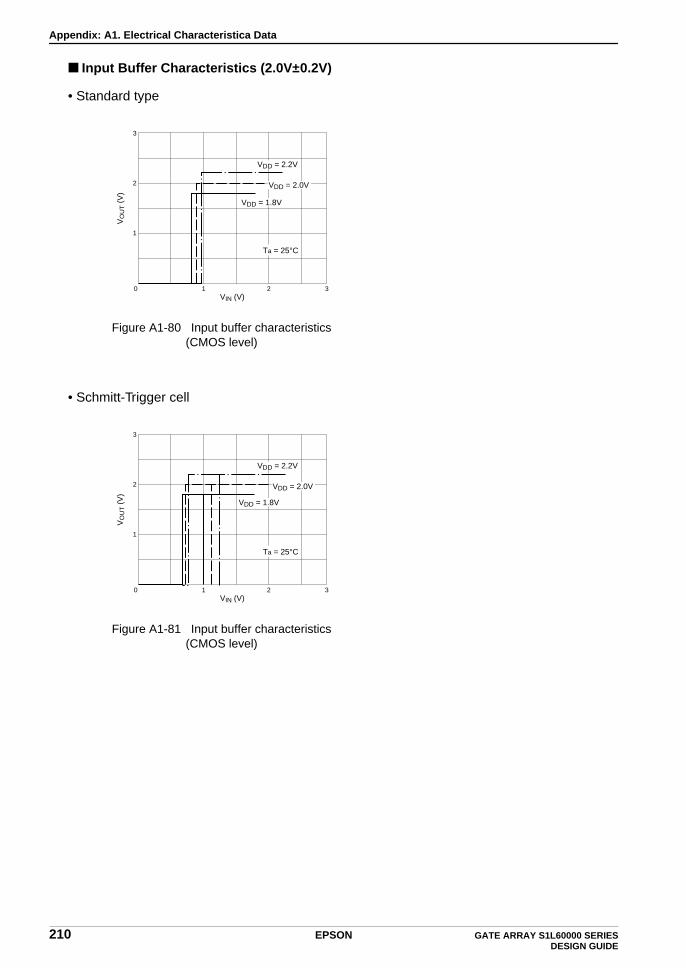
Appendix: A1. Electrical Characteristica Data
Input Buffer Characteristics (2.0V±0.2V)
• Standard type
• Schmitt-Trigger cell
Figure A1-80 Input buffer characteristics(CMOS level)
Figure A1-81 Input buffer characteristics(CMOS level)
3
2
1
1 2 3VIN (V)
VO
UT (
V)
0
Ta = 25°C
VDD = 2.2V
VDD = 2.0V
VDD = 1.8V
3
2
1
1 2 3VIN (V)
VO
UT (
V)
0
Ta = 25°C
VDD = 2.2V
VDD = 2.0V
VDD = 1.8V
210 EPSON GATE ARRAY S1L60000 SERIES DESIGN GUIDE
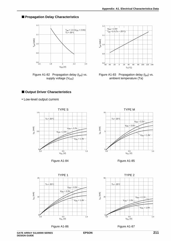
Appendix: A1. Electrical Characteristica Data
Propagation Delay Characteristics
Output Driver Characteristics
• Low-level output current
Figure A1-82 Propagation delay (tpd) vs.supply voltage (VDD)
Figure A1-83 Propagation delay (tpd) vs.ambient temperature (Ta)
Figure A1-84 Figure A1-85
Figure A1-86 Figure A1-87
1.2
1.1
1.0
0.9
0.8
Tpd
(rat
io)
1.6
VDD (V)
1.8 2 2.2 2.4
Tpd = 1.0 (VDD = 2.0V)Ta = 25°C
1.2
1.1
1.0
0.9
0.8
Tpd
(ra
tio)
-40 -20-60 200 40
Ta (°C)
60 80 100 120 140
VDD = 2.0VTpd =1.0 (Ta = 25°C)I O
L (m
A)
1.0
0.5
Ta = 25°C
1.0VOL (V)
TYPE S
0.50.00
VDD = 2.2V
VDD = 2.0V
VDD = 1.8V
I OL
(mA
)
10
5
Ta = 25°C
1.0VOL (V)
TYPE M
0.50.00
VDD = 2.2V
VDD = 2.0V
VDD = 1.8V
I OL
(mA
)
20
10
Ta = 25°C
1.0VOL (V)
TYPE 1
0.50.00
VDD = 2.2V
VDD = 2.0V
VDD = 1.8V
I OL
(mA
)
50
25
Ta = 25°C
1.0VOL (V)
TYPE 2
0.50.00
VDD = 2.2V
VDD = 2.0V
VDD = 1.8V
GATE ARRAY S1L60000 SERIES EPSON 211DESIGN GUIDE

Appendix: A1. Electrical Characteristica Data
• High-level output current
Figure A1-88 Figure A1-89
Figure A1-90
Output voltage VOH – Supply voltage VDD (V)
Figure A1-91
Output voltage VOH – Supply voltage VDD (V)
Figure A1-92
I OL
(mA
)
100
50
Ta = 25°C
1.0VOL (V)
TYPE 3
0.50.00
VDD = 2.2V
VDD = 2.0V
VDD = 1.8V
I OL
(mA
)
100
50
Ta = 25°C
1.0VOL (V)
TYPE 4
0.50.00
VDD = 2.2V
VDD = 2.0V
VDD = 1.8V
I OL
(mA
)
100
50
Ta = 25°C
1.0VOL (V)
TYPE 1 to 4
0.50.00
HVDD = 2.0VTYPE 4
TYPE 3
TYPE 2
TYPE 1
I OH
(m
A)
-1.0
-0.5
0.0
Ta = 25°C
-1.0
TYPE S
-0.5
VDD = 2.2V
VDD = 2.0V
VDD = 1.8V
I OH
(m
A)
-10
-5
0.0
Ta = 25°C
-1.0
TYPE M
-0.5
VDD = 2.2V
VDD = 2.0V
VDD = 1.8V
212 EPSON GATE ARRAY S1L60000 SERIES DESIGN GUIDE

Appendix: A1. Electrical Characteristica Data
Output voltage VOH – Supply voltage VDD (V)
Figure A1-93
Output voltage VOH – Supply voltage VDD (V)
Figure A1-94
Output voltage VOH – Supply voltage VDD (V)
Figure A1-95
Output voltage VOH – Supply voltage VDD (V)
Figure A1-96
Output voltage VOH – Supply voltage VDD (V)
Figure A1-97
I OH
(m
A)
-20
-10
0
Ta = 25°C
-1.0
TYPE 1
-0.50.0
VDD = 2.2V
VDD = 2.0V
VDD = 1.8V
I OH
(m
A)
-50
-25
0
Ta = 25°C
-1.0
TYPE 2
-0.50.0
VDD = 2.2V
VDD = 2.0V
VDD = 1.8V
I OH
(m
A)
-100
-50
0
Ta = 25°C
-1.0
TYPE 3
-0.50.0
VDD = 2.2V
VDD = 2.0V
VDD = 1.8V
I OH
(m
A)
-100
-50
0
Ta = 25°C
-1.0
TYPE 4
-0.50.0
VDD = 2.2V
VDD = 2.0V
VDD = 1.8V
I OH
(m
A)
-100
-50
0
Ta = 25°C
-1.0
TYPE 1 to 4
-0.50.0
VDD = 2.0VTYPE 4
TYPE 3
TYPE 2
TYPE 1
GATE ARRAY S1L60000 SERIES EPSON 213DESIGN GUIDE
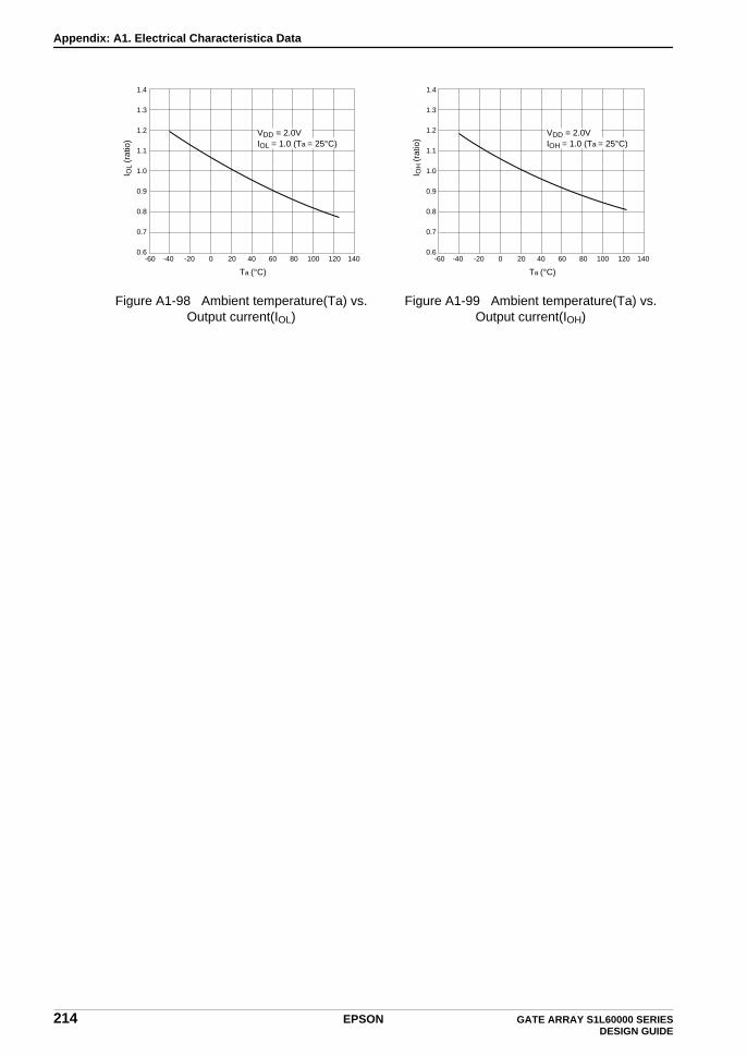
Appendix: A1. Electrical Characteristica Data
Figure A1-98 Ambient temperature(Ta) vs.Output current(IOL)
Figure A1-99 Ambient temperature(Ta) vs.Output current(IOH)
1.4
1.3
1.2
1.1
1.0
0.9
0.8
0.7
0.6
I OL
(rat
io)
-40 -20-60 200 40
Ta (°C)
60 80 100 120 140
VDD = 2.0VIOL = 1.0 (Ta = 25°C)
1.4
1.3
1.2
1.1
1.0
0.9
0.8
0.7
0.6
I OH
(rat
io)
-40 -20-60 200 40
Ta (°C)
60 80 100 120 140
VDD = 2.0VIOH = 1.0 (Ta = 25°C)
214 EPSON GATE ARRAY S1L60000 SERIES DESIGN GUIDE

Appendix: A1. Electrical Characteristica Data
Output Delay Time vs. Output Load Capacitance (CL)
Figure A1-100 Output Delay Time(tPLH) vs.Output load capacitance(CL)
Figure A1-101 Output Delay Time(tPHL) vs.Output load capacitance(CL)
Figure A1-102 Output Delay Time(tPLH) vs.Output load capacitance(CL)
Figure A1-103 Output Delay Time(tPHL) vs.Output load capacitance(CL)
0
400
300
200
100
0
CL (pF)
t
(ns
)
50 100 150 200
OBST
OBMT
VDD = 2.0VVth = 1.0VTa = 25°C
PLH
0
400
300
200
100
0
CL (pF)
t
(ns
)
50 100 150 200
OBST
OBMT
VDD = 2.0VVth = 1.0VTa = 25°C
PH
L
0
20
15
10
5
0
CL (pF)
t
(ns
)
50 100 150 200
OB1T
OB2TOB3AT
OB4AT
VDD = 2.0VVth = 1.0VTa = 25°C
PLH
0
20
15
10
5
0
CL (pF)
t
(ns
)
50 100 150 200
OB1T
OB2T
OB3AT
OB4AT
VDD = 2.0VVth = 1.0VTa = 25°C
PH
L
GATE ARRAY S1L60000 SERIES EPSON 215DESIGN GUIDE
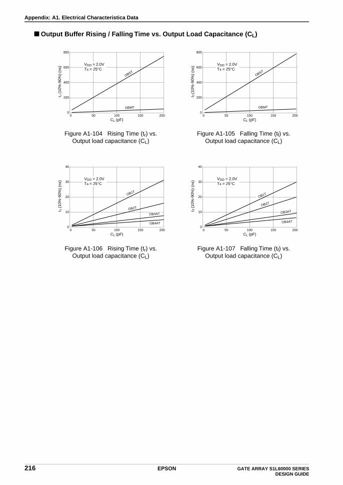
Appendix: A1. Electrical Characteristica Data
Output Buffer Rising / Falling Time vs. Output Load Capacitance (CL)
Figure A1-104 Rising Time (tr) vs.Output load capacitance (CL)
Figure A1-105 Falling Time (tf) vs.Output load capacitance (CL)
Figure A1-106 Rising Time (tr) vs.Output load capacitance (CL)
Figure A1-107 Falling Time (tf) vs.Output load capacitance (CL)
0
800
600
400
200
0
CL (pF)
t
(
ns)
50 100 150 200
OBST
OBMT
VDD = 2.0VTa = 25°C
r (1
0%-9
0%)
0
800
600
400
200
0
CL (pF)
t
(
ns)
50 100 150 200
OBST
OBMT
VDD = 2.0VTa = 25°C
f (10
%-9
0%)
0
40
30
20
10
0
CL (pF)
t
(
ns)
50 100 150 200
OB1T
OB2T
OB3AT
OB4AT
VDD = 2.0VTa = 25°C
r (1
0%-9
0%)
0
40
30
20
10
0
CL (pF)
t
(
ns)
50 100 150 200
OB1T
OB2T
OB3AT
OB4AT
VDD = 2.0VTa = 25°C
f (10
%-9
0%)
216 EPSON GATE ARRAY S1L60000 SERIES DESIGN GUIDE

Appendix: A1. Electrical Characteristica Data
Pull-Up and Pull-Down Resistance
• Pull-Up characteristics
• Pull-Down characteristics
Current Consumption Characteristics
Figure A1-108 RPLU vs. VDD characteristics Figure A1-109 RPLU vs. Ta characteristics
Figure A1-110 RPLD vs. VDD characteristics Figure A1-111 RPLD vs. Ta characteristics
Figure A1-112 IOP vs. VDD characteristics Figure A1-113 IOP vs. f(frequency) characteristics
1.6
VDD (V)
RP
LU (k
Ω)
1.8 2.0 2.2 2.4
Ta = 25°C
TYPE 1
TYPE 2
250
200
150
100
50
0-60 -40 -20 0 20 40 60 80 100 120 140
Ta (°C)
RP
LU (k
Ω)
TYPE 1
TYPE 2
200
150
100
50
0
VDD = 2.0V
1.6
VDD (V)
RP
LD (k
Ω)
1.8 2 2.2 2.4
Ta = 25°C
TYPE 1
TYPE 2
250
200
150
100
50
0-60 -40 -20 0 20 40 60 80 100 120 140
Ta (°C)
RP
LD (k
Ω)
TYPE 1
TYPE 2
200
150
100
50
0
VDD = 2.0V
1.6
VDD (V)
I OP
(ra
tio)
1.8 2 2.2 2.4
1.4
1.2
1.0
0.8
0.6
0.4
Ta = 25°CIOP = 1.0 (VDD = 2.0V)
Nor
mar
aize
d cu
rren
t con
sum
ptio
n (r
atio
)
100 1000
Frequency (kHz)
10000 100000
100.00
10.00
1.00
0.10
0.01
Ta = 25°CVDD = 2.0VIOP = 1.0 (f = 1MHz)
GATE ARRAY S1L60000 SERIES EPSON 217DESIGN GUIDE
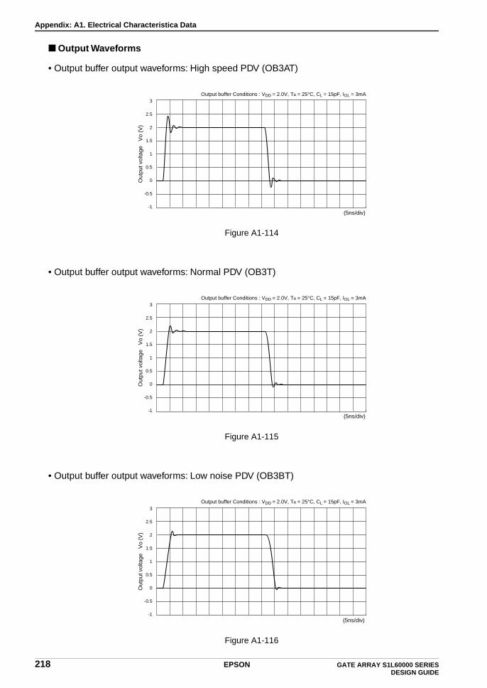
Appendix: A1. Electrical Characteristica Data
Output Waveforms
• Output buffer output waveforms: High speed PDV (OB3AT)
• Output buffer output waveforms: Normal PDV (OB3T)
• Output buffer output waveforms: Low noise PDV (OB3BT)
Figure A1-114
Figure A1-115
Figure A1-116
Output buffer Conditions : VDD = 2.0V, Ta = 25°C, CL = 15pF, IOL = 3mA3
2.5
2
1.5
1
0.5
0
-0.5
-1
Out
put v
olta
ge
Vo
(V)
(5ns/div)
Output buffer Conditions : VDD = 2.0V, Ta = 25°C, CL = 15pF, IOL = 3mA3
2.5
2
1.5
1
0.5
0
-0.5
-1
Out
put v
olta
ge
Vo
(V)
(5ns/div)
Output buffer Conditions : VDD = 2.0V, Ta = 25°C, CL = 15pF, IOL = 3mA3
2.5
2
1.5
1
0.5
0
-0.5
-1
Out
put v
olta
ge
Vo
(V)
(5ns/div)
218 EPSON GATE ARRAY S1L60000 SERIES DESIGN GUIDE

Appendix: A1. Electrical Characteristica Data
A1.4 Estimated Wiring Load Table
The following shows the virtual wiring capacity load used in a prewiring simulation. Refer to this table when you calculate the delay. (See "3. DELAY CALCULATION")Note: The 3-layer wiring and 4-layer wiring have different values.
Table A1-4 Virtual load capacity of 3-layer wiring[LU]
Numberof nodes
Type
S1L60093
S1L60173
S1L60283
S1L60403
S1L60593
S1L60833
S1L61233
S1L61583
S1L61903
S1L62513
1 1.6 1.6 1.7 1.8 2.0 2.1 2.4 2.7 2.9 3.4
2 3.2 3.3 3.5 3.6 3.9 4.3 4.8 5.4 5.8 6.7
3 4.8 4.9 5.2 5.4 5.9 6.4 7.3 8.0 8.7 10.1
4 6.4 6.6 6.9 7.2 7.8 8.5 9.7 10.7 11.6 13.4
5 7.9 8.2 8.6 9.0 9.8 10.6 12.1 13.4 14.6 16.8
6 9.5 9.9 10.4 10.9 11.7 12.8 14.5 16.1 17.5 20.2
7 11.1 11.5 12.1 12.7 13.7 14.9 16.9 18.8 20.4 23.5
8 12.7 13.1 13.8 14.5 15.6 17.0 19.4 21.4 23.3 26.9
9 14.3 14.8 15.5 16.3 17.6 19.1 21.8 24.1 26.2 30.3
10 15.9 16.4 17.3 18.1 19.5 21.3 24.2 26.8 29.1 33.6
11 17.5 18.1 19.0 19.9 21.5 23.4 26.6 29.5 32.0 37.0
12 19.1 19.7 20.7 21.7 23.4 25.5 29.1 32.2 34.9 40.3
13 20.7 21.4 22.4 23.5 25.4 27.6 31.5 34.8 37.8 43.7
14 22.3 23.0 24.2 25.3 27.3 29.8 33.9 37.5 40.7 47.1
15 23.8 24.6 25.9 27.1 29.3 31.9 36.3 40.2 43.7 50.4
16 25.4 26.3 27.6 29.0 31.2 34.0 38.7 42.9 46.6 53.8
17 27.0 27.9 29.3 30.8 33.2 36.1 41.2 45.6 49.5 57.2
18 28.6 29.6 31.1 32.6 35.2 38.3 43.6 48.2 52.4 60.5
19 30.2 31.2 32.8 34.4 37.1 40.4 46.0 50.9 55.3 63.9
20 31.8 32.9 34.5 36.2 39.1 42.5 48.4 53.6 58.2 67.2
21 33.4 34.5 36.2 38.0 41.0 44.6 50.8 56.3 61.1 70.6
22 35.0 36.1 38.0 39.8 43.0 46.8 53.3 59.0 64.0 74.0
23 36.6 37.8 39.7 41.6 44.9 48.9 55.7 61.6 66.9 77.3
24 38.1 39.4 41.4 43.4 46.9 51.0 58.1 64.3 69.9 80.7
25 39.7 41.1 43.1 45.2 48.8 53.1 60.5 67.0 72.8 84.1
26 41.3 42.7 44.9 47.1 50.8 55.3 62.9 69.7 75.7 87.4
27 42.9 44.3 46.6 48.9 52.7 57.4 65.4 72.4 78.6 90.8
28 44.5 46.0 48.3 50.7 54.7 59.5 67.8 75.0 81.5 94.1
29 46.1 47.6 50.0 52.5 56.6 61.6 70.2 77.7 84.4 97.5
30 47.7 49.3 51.8 54.3 58.6 63.8 72.6 80.4 87.3 100.9
GATE ARRAY S1L60000 SERIES EPSON 219DESIGN GUIDE
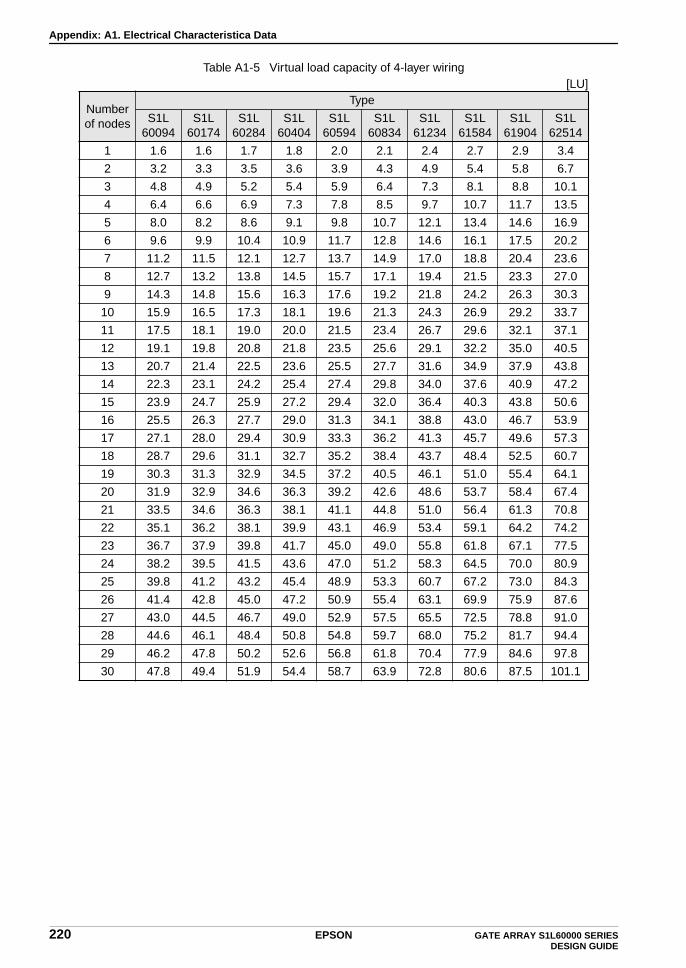
Appendix: A1. Electrical Characteristica Data
Table A1-5 Virtual load capacity of 4-layer wiring[LU]
Numberof nodes
Type
S1L60094
S1L60174
S1L60284
S1L60404
S1L60594
S1L60834
S1L61234
S1L61584
S1L61904
S1L62514
1 1.6 1.6 1.7 1.8 2.0 2.1 2.4 2.7 2.9 3.4
2 3.2 3.3 3.5 3.6 3.9 4.3 4.9 5.4 5.8 6.7
3 4.8 4.9 5.2 5.4 5.9 6.4 7.3 8.1 8.8 10.1
4 6.4 6.6 6.9 7.3 7.8 8.5 9.7 10.7 11.7 13.5
5 8.0 8.2 8.6 9.1 9.8 10.7 12.1 13.4 14.6 16.9
6 9.6 9.9 10.4 10.9 11.7 12.8 14.6 16.1 17.5 20.2
7 11.2 11.5 12.1 12.7 13.7 14.9 17.0 18.8 20.4 23.6
8 12.7 13.2 13.8 14.5 15.7 17.1 19.4 21.5 23.3 27.0
9 14.3 14.8 15.6 16.3 17.6 19.2 21.8 24.2 26.3 30.3
10 15.9 16.5 17.3 18.1 19.6 21.3 24.3 26.9 29.2 33.7
11 17.5 18.1 19.0 20.0 21.5 23.4 26.7 29.6 32.1 37.1
12 19.1 19.8 20.8 21.8 23.5 25.6 29.1 32.2 35.0 40.5
13 20.7 21.4 22.5 23.6 25.5 27.7 31.6 34.9 37.9 43.8
14 22.3 23.1 24.2 25.4 27.4 29.8 34.0 37.6 40.9 47.2
15 23.9 24.7 25.9 27.2 29.4 32.0 36.4 40.3 43.8 50.6
16 25.5 26.3 27.7 29.0 31.3 34.1 38.8 43.0 46.7 53.9
17 27.1 28.0 29.4 30.9 33.3 36.2 41.3 45.7 49.6 57.3
18 28.7 29.6 31.1 32.7 35.2 38.4 43.7 48.4 52.5 60.7
19 30.3 31.3 32.9 34.5 37.2 40.5 46.1 51.0 55.4 64.1
20 31.9 32.9 34.6 36.3 39.2 42.6 48.6 53.7 58.4 67.4
21 33.5 34.6 36.3 38.1 41.1 44.8 51.0 56.4 61.3 70.8
22 35.1 36.2 38.1 39.9 43.1 46.9 53.4 59.1 64.2 74.2
23 36.7 37.9 39.8 41.7 45.0 49.0 55.8 61.8 67.1 77.5
24 38.2 39.5 41.5 43.6 47.0 51.2 58.3 64.5 70.0 80.9
25 39.8 41.2 43.2 45.4 48.9 53.3 60.7 67.2 73.0 84.3
26 41.4 42.8 45.0 47.2 50.9 55.4 63.1 69.9 75.9 87.6
27 43.0 44.5 46.7 49.0 52.9 57.5 65.5 72.5 78.8 91.0
28 44.6 46.1 48.4 50.8 54.8 59.7 68.0 75.2 81.7 94.4
29 46.2 47.8 50.2 52.6 56.8 61.8 70.4 77.9 84.6 97.8
30 47.8 49.4 51.9 54.4 58.7 63.9 72.8 80.6 87.5 101.1
220 EPSON GATE ARRAY S1L60000 SERIES DESIGN GUIDE
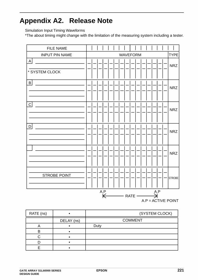
GATE ARRAY S1L60000 SERIES EPSON 221DESIGN GUIDE
Appendix A2. Release NoteSimulation Input Timing Waveforms*The about timing might change with the limitation of the measuring system including a tester.
A
FILE NAME
TYPEWAVEFORMINPUT PIN NAME
NRZ
BNRZ
CNRZ
DNRZ
NRZ
STROBE
* SYSTEM CLOCK
STROBE POINT
RATEA.PA.P
A.P = ACTIVE POINT
ABCDE
RATE (ns)
COMMENT
•
DELAY (ns)
(SYSTEM CLOCK)
•
•••
•
Duty
International Sales Operations
AMERICA
EPSON ELECTRONICS AMERICA, INC.- HEADQUARTERS -150 River Oaks ParkwaySan Jose, CA 95134, U.S.A.Phone: +1-408-922-0200 Fax: +1-408-922-0238
- SALES OFFICES -West1960 E. Grand AvenueEI Segundo, CA 90245, U.S.A.Phone: +1-310-955-5300 Fax: +1-310-955-5400
Central101 Virginia Street, Suite 290Crystal Lake, IL 60014, U.S.A.Phone: +1-815-455-7630 Fax: +1-815-455-7633
Northeast301 Edgewater Place, Suite 120Wakefield, MA 01880, U.S.A.Phone: +1-781-246-3600 Fax: +1-781-246-5443
Southeast3010 Royal Blvd. South, Suite 170Alpharetta, GA 30005, U.S.A.Phone: +1-877-EEA-0020 Fax: +1-770-777-2637
- DESIGN SUPPORT CENTERS -San Jose Asic Design Center150 River Oaks ParkwaySan Jose, CA 95134, U.S.A.Phone: +1-408-922-0200 Fax: +1-408-922-0238
EUROPE
EPSON EUROPE ELECTRONICS GmbH- HEADQUARTERS -Riesstrasse 1580992 Munich, GERMANYPhone: +49-(0)89-14005-0 Fax: +49-(0)89-14005-110
DÜSSELDORF BRANCH OFFICEAltstadtstrasse 17651379 Leverkusen, GERMANYPhone: +49-(0)2171-5045-0 Fax: +49-(0)2171-5045-10
UK & IRELAND BRANCH OFFICEUnit 2.4, Doncastle House, Doncastle RoadBracknell, Berkshire RG12 8PE, ENGLANDPhone: +44-(0)1344-381700 Fax: +44-(0)1344-381701
FRENCH BRANCH OFFICE1 Avenue de l’ Atlantique, LP 915 Les ConquerantsZ.A. de Courtaboeuf 2, F-91976 Les Ulis Cedex, FRANCEPhone: +33-(0)1-64862350 Fax: +33-(0)1-64862355
BARCELONA BRANCH OFFICE
Barcelona Design CenterEdificio TestaAdva. Alcalde Barrils num. 64-68E-08190 Sant Cugat del Vallès, SPAINPhone: +34-93-544-2490 Fax: +34-93-544-2491
Scotland Design CenterIntegration House, The Alba Campus Livingston West Lothian, EH54 7EG, SCOTLANDPhone: +44-1506-605040 Fax: +44-1506-605041
ASIA
EPSON (CHINA) CO., LTD.23F, Beijing Silver Tower 2# North RD DongSanHuan ChaoYang District, Beijing, CHINAPhone: 64106655 Fax: 64107319
SHANGHAI BRANCH7F, High-Tech Bldg., 900, Yishan Road, Shanghai 200233, CHINAPhone: 86-21-5423-5577 Fax: 86-21-5423-4677
EPSON HONG KONG LTD.20/F., Harbour Centre, 25 Harbour RoadWanchai, Hong KongPhone: +852-2585-4600 Fax: +852-2827-4346Telex: 65542 EPSCO HX
EPSON TAIWAN TECHNOLOGY & TRADING LTD.14F, No. 7, Song Ren Road, Taipei 110Phone: 02-8786-6688 Fax: 02-8786-6660
HSINCHU OFFICE 13F-3, No. 295, Kuang-Fu Road, Sec. 2HsinChu 300Phone: 03-573-9900 Fax: 03-573-9169
EPSON SINGAPORE PTE., LTD.No. 1 Temasek Avenue, #36-00Millenia Tower, SINGAPORE 039192Phone: +65-6337-7911 Fax: +65-6334-2716
SEIKO EPSON CORPORATIONKOREA OFFICE50F, KLI 63 Bldg., 60 Yoido-dongYoungdeungpo-Ku, Seoul, 150-763, KOREAPhone: 02-784-6027 Fax: 02-767-3677
GUMI OFFICE6F, Good Morning Securities Bldg. 56 Songjeong-Dong, Gumi-City, 730-090, KOREAPhone: 054-454-6027 Fax: 054-454-6093
SEIKO EPSON CORPORATIONELECTRONIC DEVICES MARKETING DIVISION
IC Marketing Department IC Marketing & Engineering Group421-8, Hino, Hino-shi, Tokyo 191-8501, JAPANPhone: +81-(0)42-587-5816 Fax: +81-(0)42-587-5624
ED International Marketing Department 421-8, Hino, Hino-shi, Tokyo 191-8501, JAPANPhone: +81-(0)42-587-5814 Fax: +81-(0)42-587-5117
DESIGN GUIDES1L60000 Series
First issue May,1998 DPrinted February, 2003 in Japan C A
EPSON Electronic Devices Website
ELECTRONIC DEVICES MARKETING DIVISION
http://www.epsondevice.com
Document code: 404508004
This manual was made with recycle papaer, and printed using soy-based inks.