GaN has emerged as the technology of choice for power ...
22
1 Corporate presentation 2013-06-06 1 GaN has emerged as the technology of choice for power conversion in green transport applications Geoff Haynes Vice President Business Development
Transcript of GaN has emerged as the technology of choice for power ...

1
Corporate presentation 2013-06-06
1
GaN has emerged as the technology of choice for power conversion in green transport applications Geoff Haynes Vice President Business Development
2
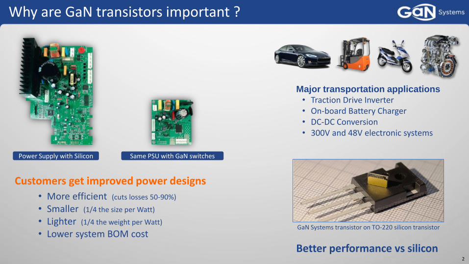
Why are GaN transistors important ?
Power Supply with Silicon Same PSU with GaN switches
Customers get improved power designs
• More efficient (cuts losses 50-90%)
• Smaller (1/4 the size per Watt)
• Lighter (1/4 the weight per Watt)
• Lower system BOM cost
Major transportation applications • Traction Drive Inverter • On-board Battery Charger • DC-DC Conversion • 300V and 48V electronic systems
Better performance vs silicon
GaN Systems transistor on TO-220 silicon transistor

3
• True Enhancement-Mode - Normally Off • Industry’s highest current ratings • 45x better FOM than 650V MOSFETs or IGBTs • 15x better FOM than 100V MOSFETs • +10V Gate tolerance – uses MOSFET drivers • Drive Assist™ on high-current devices • GaNPX™ packaging for ultra-low inductance
Switches to fit all applications
4
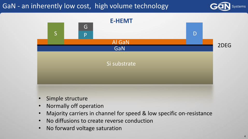
GaN - an inherently low cost, high volume technology
Si substrate
GaN Al GaN
S D G
2DEG
P
E-HEMT
• Simple structure • Normally off operation • Majority carriers in channel for speed & low specific on-resistance • No diffusions to create reverse conduction • No forward voltage saturation

5
GaN e-Mode Reverse Conduction Advantage
• Reverse conduction is an intrinsic operation of a GaN e-Mode – no Fast Recovery Diodes are required
• There are no diffusions so there is zero Qrr
• When the GaN e-Mode active switch mode is used, as shown, very low losses are achieved because the ‘diode like’ offsets are eliminated
GaN e-Mode forward & reverse conduction
6
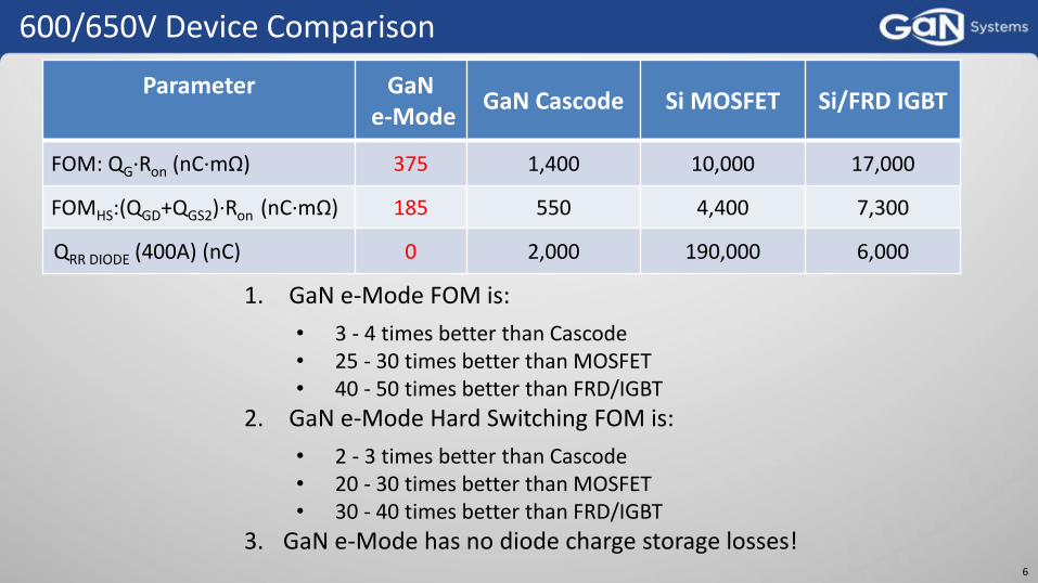
600/650V Device Comparison
1. GaN e-Mode FOM is:
• 3 - 4 times better than Cascode • 25 - 30 times better than MOSFET • 40 - 50 times better than FRD/IGBT
2. GaN e-Mode Hard Switching FOM is:
• 2 - 3 times better than Cascode • 20 - 30 times better than MOSFET • 30 - 40 times better than FRD/IGBT
3. GaN e-Mode has no diode charge storage losses!
Parameter
GaN e-Mode
GaN Cascode Si MOSFET Si/FRD IGBT
FOM: QG·Ron (nC·mΩ) 375 1,400 10,000 17,000
FOMHS:(QGD+QGS2)·Ron (nC·mΩ) 185 550 4,400 7,300
QRR DIODE (400A) (nC) 0 2,000 190,000 6,000

7
• Full bridge total power loss using GaN @100kHz: • 9x better than CoolMOS • 7x better than IGBT • 2x better than SiC
• Full bridge total power loss using GaN
@1MHz • 3x better than SiC • Not possible with IGBT or CoolMOS
Inverter system: 2 kVA, 400VDC input, 240V/8.3A 60Hz output, p.f. = 0.9
Heatsink temperature THS,max = 60C
TO-220/TO-247 Package: Thermal insulation material Rth_TIM ~=1°C/W
GaN EHEMT: 4-layer FR4 PCB bottom side cooling using thermal vias: Rth_PCB ~= 5°C/W
More efficient, smaller & lighter
Power losses are simulated using Pspice model or calculated using datasheet parameters
GaN
SiC
Silicon
• GaN shows lower power loss over all switching frequencies
8
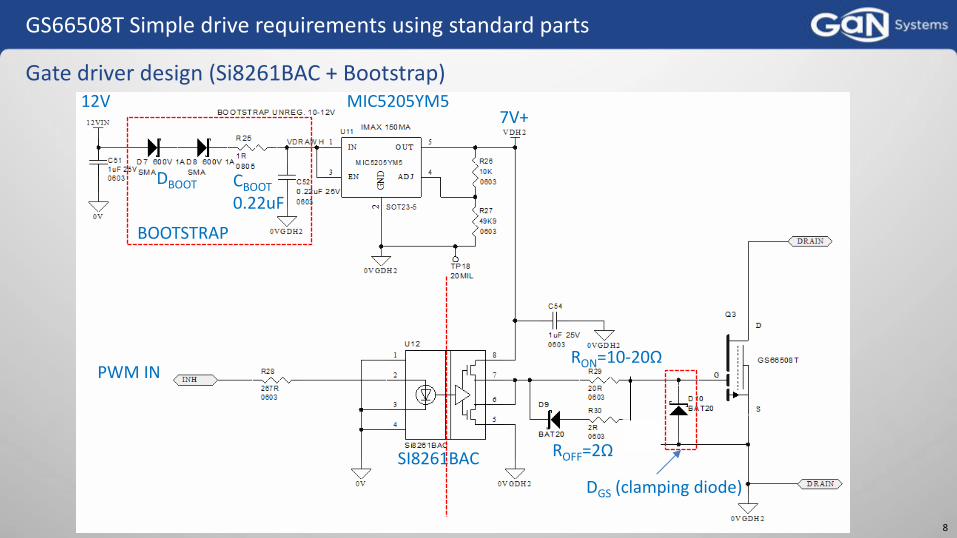
GS66508T Simple drive requirements using standard parts
Gate driver design (Si8261BAC + Bootstrap)
SI8261BAC
MIC5205YM5
BOOTSTRAP
RON=10-20Ω
7V+ 12V
CBOOT
0.22uF
DBOOT
ROFF=2Ω
PWM IN
DGS (clamping diode)
.
9
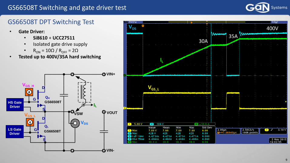
GS66508T Switching and gate driver test
GS66508T DPT Switching Test VDS
IL
VGS_L
400V
30A
• Gate Driver: • Si8610 + UCC27511 • Isolated gate drive supply • RON = 10Ω / ROFF = 2Ω
• Tested up to 400V/35A hard switching
35A
D
S
D
S
VSW
QH
GS66508T
VIN+
HS Gate
Driver
LS Gate
Driver
G
GQL
GS66508T
VIN-
VOUT
VDS
IL
VGS_L
VGS_H

10
GS66508T Switching and gate driver test
Double Pulse Test
Turn-on (400V/30A) Turn-off (400V/35A)
VDS
IL
VGS_L
Tfall = 7.3ns 55V/ns
Trise = 4.6ns ~90V/ns
VPK = 428V
• Gate driver UCC27511: RON = 10Ω / ROFF = 2Ω • Top-side cooled package makes the tight layout possible: Low drain voltage overshoot • Clean gate waveform

11
100 V E-HEMT vs 100 V OptiMOS - Faster switching & no reverse charge
36 V to 12 V buck converter power loss comparison
Symmetric • Same device on high/low sides • GaN EHEMT:
• GS61008P V2 (100V,7.4mΩ) • Si MOSFET:
• BSC070N10NS5 (100V,7mΩ)
GaN
Silicon
• GaN shows overall better efficiency & lower power loss

12
E-HEMT vs OptiMOS - Faster switching & no reverse charge
Power Loss Breakdown
TJ = 39°C TJ = 39°C
TJ = 75°C
TJ = 36°C
• GaN: GS61008P (100V, 7.4mΩ)
• OptiMOS: BSC070N10NS5 (100V, 7mΩ)
• IOUT = 10A, POUT = 120W
• Case-Ambient (PCB) Thermal resistance Rth,C-A = 20°C/W
• High Side: GaN has lower switching loss and zero reverse recovery loss
• Low Side: GaN has higher dead time conduction loss
• GaN shows lower total power loss & lower junction temperature TJ

13
Island Technology® road map - High current structures
Island Technology® enables commercialization of higher current GaN switches
• High yields • High currents
• 100 V – 250 A • 650 V – 200 A
• High speeds
• Low costs
• Low inductance packaging Isolated island structure

14
650 V 60 A switch in top-side cooled GaNPX™ pack
• 8.95 mm x 7.59mm x 0.5mm
• Reduced thermal resistance
• Shorter vias to improve Rds(on) & Inductance
• Dual Gate connections to optimise layout for high switching frequency
• Available now
15
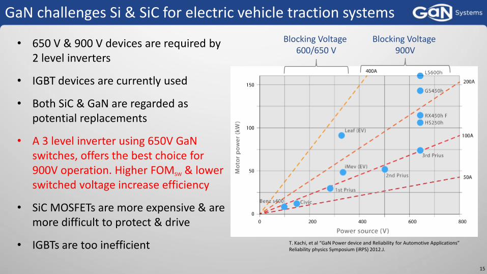
GaN challenges Si & SiC for electric vehicle traction systems
Blocking Voltage 600/650 V
Blocking Voltage 900V
• 650 V & 900 V devices are required by 2 level inverters
• IGBT devices are currently used
• Both SiC & GaN are regarded as potential replacements
• A 3 level inverter using 650V GaN switches, offers the best choice for 900V operation. Higher FOMSW & lower switched voltage increase efficiency
• SiC MOSFETs are more expensive & are more difficult to protect & drive
• IGBTs are too inefficient T. Kachi, et al “GaN Power device and Reliability for Automotive Applications” Reliability physics Symposium (iRPS) 2012.J.

16
• Addition of 48 V power system in new vehicles is reducing wiring harness current, weight & voltage drop
• The GS61040 250 A, 100 V, 2.4 mΩ high speed E-GaN switch enables: • Higher efficiency • Air cooling • Lower component count • Smaller passive components
100V, 250 Amp switch ideal for 12 V 48 V conversion

Immunity to single event failure
• Single event cosmic radiation causes failure in Si power systems A single particle impact while switching can destroy an IGBT Significant voltage de-rating of IGBTs is needed to maintain reliability
• GaN E-HEMTs do not suffer from this effect E-HEMT majority carrier channel is intrinsically radiation-resistant 2014 IEEE paper by Leif Scheick, NASA Confirmed E-HEMT radiation immunity in power circuits
• Testing of GaN Systems devices is underway High dose with devices energized - 800 MeV protons, 0.3 x 10¹⁴ protons/cm2 Initial results – devices unaffected
• What does this mean in practice? Increased reliability No need for de-rating in critical applications
IGBT radiation de-rating curve at sea level

18
DRS Technologies - 2 kW vehicle power inverter
• 94% Efficient
• 28 Volt DC
• 3 phase 120 Volt AC
• Passive cooling
• Reduced part count
• Uses GaN Systems GS66508P
Production Systems
19
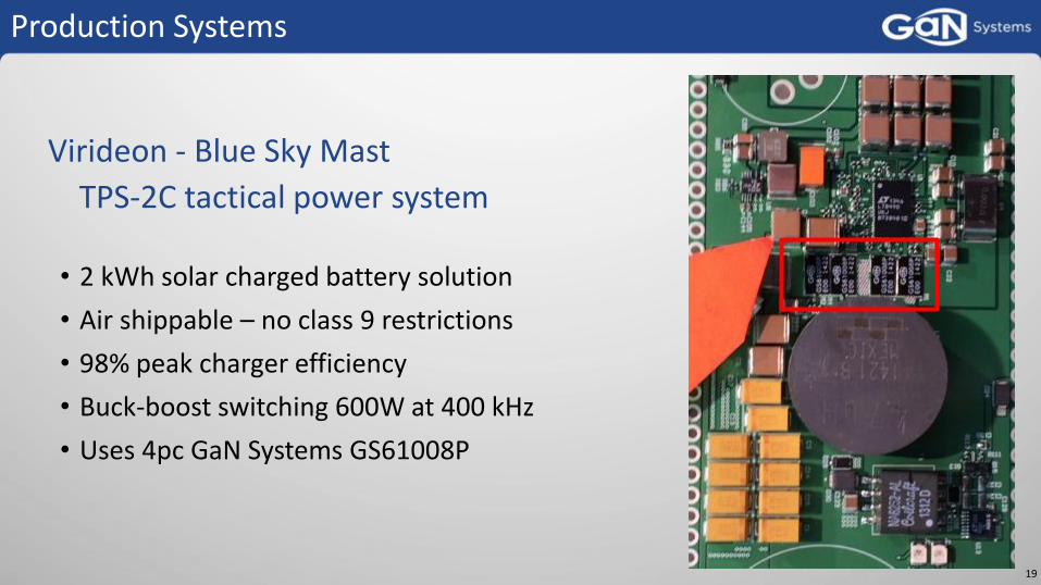
• 2 kWh solar charged battery solution
• Air shippable – no class 9 restrictions
• 98% peak charger efficiency
• Buck-boost switching 600W at 400 kHz
• Uses 4pc GaN Systems GS61008P
Virideon - Blue Sky Mast
TPS-2C tactical power system
Production Systems

20
NEXTHOME consortium - Bi directional converter
• 3 k Watt
• 800 Volt link voltage
• 2 MHz switching fq.
• 98% efficiency
• Passive cooling
Production Systems

21
Where are GaN transistors important ?
Power Supply with Silicon Same PSU with GaN switches
Customers get improved power designs
• More efficient (cuts losses 50-90%)
• Smaller (1/4 the size per Watt)
• Lighter (1/4 the weight per Watt)
• Lower system BOM & operating cost
In all power conversion applications from 100 Watts to 100,000 Watts with operating voltages to 900V
Better performance vs silicon
GaN Systems transistor on TO-220 silicon transistor

22
www.gansystems.com • North America • Europe • Asia
Tomorrow’s power today®