GaN and Ultra Wide Bandgap III-Nitrides for Power Electronics · Ultra Wide Bandgap Semiconductors...
22
Transcript of GaN and Ultra Wide Bandgap III-Nitrides for Power Electronics · Ultra Wide Bandgap Semiconductors...

• Current GaN Power Devices and Performance
• Technological challenges and opportunities for GaN:
• Device Passivation
• N-Polar vs. Ga-Polar
• Ion Implantation
• Ultra Wide Bandgap III-Nitrides (AlGaN AlN)
• Device demonstrations
• Contacts
• Making III-Nitride technology accessible at NCSU
Outline
22019 FREEDM Research Symposium

GaN for Power
32019 FREEDM Research Symposium
• GaN Power Device market size expected to surpass $400M by 2022
• Compared to SiC’s ~$1B market size in 2022
• BUT the GaN for RF market is projected to reach $1.3B by 2023
• BUT the GaN-based optoelectronics market is also growing >$1B
idealon
2
R
4BVBFOM
B. J. Baliga, Fundamentals of Power Semiconductor Devices, 2nd ed. Boston, MA: Springer International Publishing AG, 2019.
https://epc-co.com/epc/DesignSupport/ApplicationNotes/AN003-UsingEnhancementMode.aspx
http://www.yole.fr/iso_album/illus_power_gan_market_applications_yole_oct2017_updated.jpg

Lateral AlGaN/GaN HEMTs
4
• AlGaN/GaN heterojunction creates
quantum well (2DEG) with high
electron mobility
• 2DEG is polarization doped:
• Spontaneous polarization
• Piezoelectric polarization
• AlGaN/GaN HEMTs are normally-
on devices
• Heteroepitaxially grown on Si, SiC
or Sapphire substrates
2019 FREEDM Research Symposium
E-Mode AlGaN/GaN HEMTs
52019 FREEDM Research Symposium
F. Medjdoub, Gallium Nitride (GaN): Physics, Devices, and Technology, vol. 47. CRC Press, 2015.
Recessed Gate Fluorinated Gate P-(Al)GaN Gate Cascode/Baliga Pair

Commercialization Gap
6
ProductResearch
2019 FREEDM Research Symposium
2006
2007
50-600V
6.6 W/mm

Thermal Management
72019 FREEDM Research Symposium
GaN
Del Alamo, Microelectronics Reliability, 2009
IV degradation due to Self-Heating
Constant 28 V Drain Bias
Pavlidis et al., IEEE TED, 64 (1), 78-83, 2017
Advanced
Characterization
Gate Resistance
Thermometry
Advanced
Cooling
“ICECool”
GaN on Diamond
K. Hirama, Appl. Phys. Lett., vol. 98, no. 16, p.
162112, Apr. 2011.
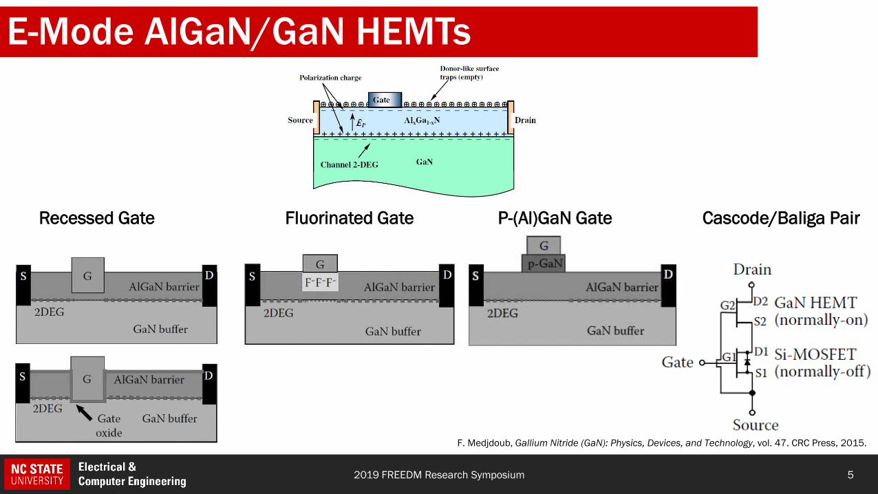
AlGaN/GaN HEMT Passivation
8
• Two challenges:
• N- bond is less stable than O-bond
• GaOx forms on the surface
• Charged surface states on the
surface
• Transient effects
• Fermi level pinning
What materials and device
fabrication techniques can we use
to passivate?
2019 FREEDM Research Symposium

SiNx Passivation
92019 FREEDM Research Symposium
w/ Nitridation w/o Nitridation
S. Yang et al., IEEE Electron Device Letters, vol. 34, no. 12, pp. 1497–1499, 2013.
H. Sun et al., IEEE Transactions on Electron Devices, vol. 65, no. 11, pp. 4814–4819, Nov. 2018.
J. Gao et al., IEEE Transactions on Electron Devices, vol. 65, no. 5, pp. 1728–1733, May 2018.
• In-situ nitridation ensures a clean interface between AlGaN and passivation
• LPCVD SiNx process offers ex-situ nitridation and high-quality passivation
Produced in a 150mm Si foundry

• Forward bias non-idealities in photolithography-processed SBDs are reduced via anneal
• Shadow-masked contacts show superior reverse leakage performance
• Acid treatment prior to metal deposition yields ideal Schottky diode behavior
Temperature Instability due to Poor Interfaces
102019 FREEDM Research Symposium
P. Reddy et al., “Defect-free Ni/GaN Schottky barrier behavior with high temperature stability,” Applied Physics Letters, vol. 110, no. 1, p. 011603, 2017.
Photolithography
Original Post-Anneal
Ideal Diode w/ Acid TreatmentShadow-Mask

N-Polar GaN
11
Curiosity Performance
O. Ambacher et al., Journal of Applied Physics, vol. 85, no. 6, pp. 3222–3233, 1999.
R. Collazo, et al., Applied Physics Letters, vol. 91, no. 21, p. 212103, 2007.
S. Wienecke et al., IEEE Electron Device Letters, vol. 37, no. 6, pp. 713–716, 2016.
Non-equivalent properties
Lower contact
resistance improves
output power!

What about N-GaN surfaces?
12
StepSample 1
(Control)
Sample 2
(Treated)
Ohmic ContactShadow Mask
(V/Al/Ni/Au)
Shadow Mask
(V/Al/Ni/Au)
Schottky Contact
Patterning MethodShadow Mask Lithography
Surface Treatment --- Boiling HCl:H2O
Schottky Metal
DepositionNi Ni
Lift-Off ---NMP (at 70°C)
then acetone & IPA
• MOCVD-grown N-polar GaN on sapphire
• O2-doped
D. Khachariya et al., “Chemical Treatment Effects on Schottky
Contacts to MOCVD N-polar GaN,” presented at the International Workshop on Nitride Semiconductors, Kanazawa, Japan, 2018.

0.0 0.2 0.4 0.6 0.8 1.010-3
10-2
10-1
100
101
102
103
Cu
rren
t D
en
sit
y (
A/c
m2)
Voltage (V)
I-V Comparison
13
Processed SampleControl Sample
ΦB = 0.4 eV
n = 1.08
Near-ideal ideality factor via shadow masking
0.0 0.2 0.4 0.6 0.8 1.0 1.210-5
10-4
10-3
10-2
10-1
100
101
102
0.87eV - Simulated
0.3eV - SimulatedExperimental IV
Cu
rren
t D
en
sit
y (
A/c
m2)
Voltage (V)
Defective surface introduces non-idealities
We need passivation!D. Khachariya et al., “Chemical Treatment Effects on Schottky Contacts to MOCVD N-polar GaN,” presented at the International Workshop on Nitride Semiconductors, Kanazawa, Japan, 2018.

Ion Implantation Technology for GaN
14
Mg-Implantation for p-GaNAr implantation for edge termination
2019 FREEDM Research Symposium
BV =
1.65 kV
Activation anneal is critical
A. M. Ozbek and B. J. Baliga, “Planar Nearly Ideal Edge-Termination
Technique for GaN Devices,” IEEE
Electron Device Letters, vol. 32, no. 3,
pp. 300–302, 2011.
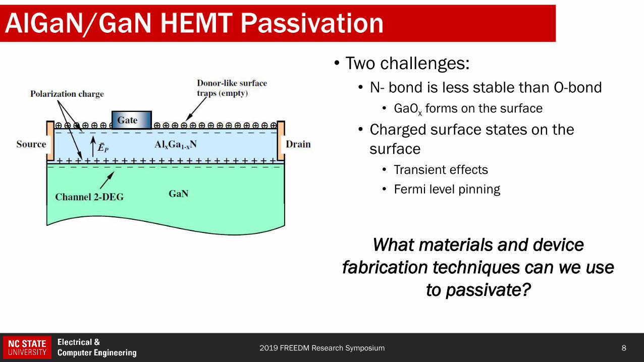
Ultra Wide Bandgap Semiconductors
15
J. Y. Tsao et al., “Ultrawide-Bandgap Semiconductors: Research Opportunities and Challenges,” Advanced Electronic Materials, vol. 4, no. 1, p. 1600501, 2018.
Ultra WBG III-Nitrides (AlGaN and AlN) offer
the next frontier of power electronics, and are
once again supported by optoelectronics
applications (e.g., UV water purification)
ECE 792-047: Ultra Wide Bandgap Semiconductors

Ιοn-Implanted AlN Channels
162019 FREEDM Research Symposium
AlN (500 nm)
Si Si Si Si
AlN or Sapphire Substrate
-40 -20 0 20 40
-1.0E-06
-5.0E-07
0.0E+00
5.0E-07
1.0E-06
Cu
rre
nt
(A)
Voltage (Volts)
Titanium
Vanadium
Si implantation
n-type dopes AlN
V-based ohmic contacts
outperform traditional
Ti-based contacts
1.4 1.8 2.2 2.6 3.0 3.4
1E-02
1E-01
1E+00
Implanted AlN:Si
MOCVD AlN:Si
Co
nd
uctivity (
-1cm
-1)
1000/T (K-1)
700 500 300
Temperature (K)
Ion implantation in AlN
provides a pathway to higher
ND than epitaxial doping
M. H. Breckenridge et al., “Electrical and Structural Characterization of Si Implanted Homoepitaxially Grown AlN,” in 2018 IEEE Research
and Applications of Photonics In Defense Conference (RAPID), 2018, pp. 1–4.
Activation anneal recipe is critical!
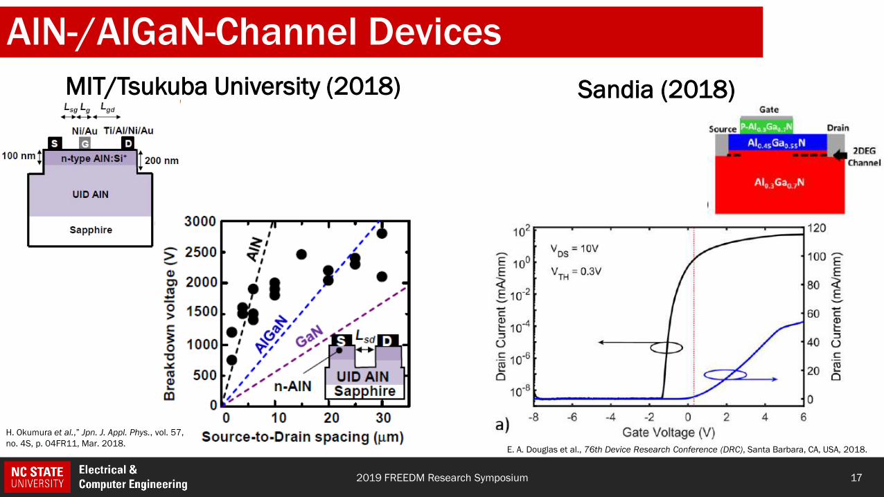
AlN-/AlGaN-Channel Devices
17
Sandia (2018)MIT/Tsukuba University (2018)
2019 FREEDM Research Symposium
E. A. Douglas et al., 76th Device Research Conference (DRC), Santa Barbara, CA, USA, 2018.
H. Okumura et al.,” Jpn. J. Appl. Phys., vol. 57,
no. 4S, p. 04FR11, Mar. 2018.
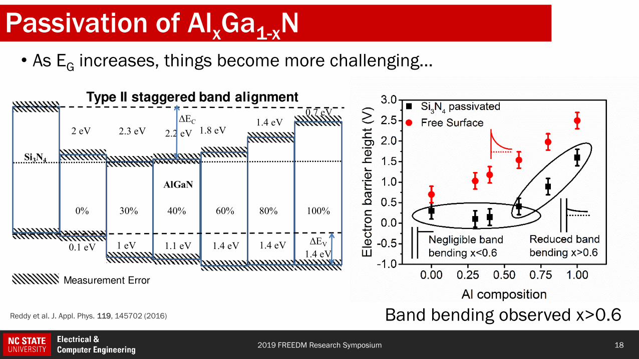
• As EG increases, things become more challenging…
Passivation of AlxGa1-xN
182019 FREEDM Research Symposium
AlGaN
1.4 eV
ΔEV
1.4 eVΔEC
1.4 eV1.1 eV 1.4 eV1 eV
0.7 eV
0.1 eV
0% 30% 40% 60% 80% 100%
Si3N4
2.3 eV2 eV 1.8 eV2.2 eV
Type II staggered band alignment
Measurement Error
Reddy et al. J. Appl. Phys. 119, 145702 (2016) Band bending observed x>0.6

Fabrication Capabilities
192019 FREEDM Research Symposium
WBG Device Fabrication Course (& Industry Short Course?)
AlGaN
E-Mode AlGaN/GaN MIS-HEMT
S DG
1E-11
1E-10
1E-9
1E-8
1E-7
1E-6
1E-5
1E-4
1E-3
1E-2
1E-1
2 4 6 8
Cu
rren
t, I
(A
)
Gate-Source Voltage, VGS (V)
Drain Current
Gate Current

Measurement Capabilities
202019 FREEDM Research Symposium
On-Wafer DC I-V High-Power, High-Speed PIV
220V / 2A / 200 ns PW
2kV / 100A / 1 µsec PW
Transient
1 GHz BW

• AlGaN/GaN HEMTs are rapidly penetrating the power device market
• But we are leaving performance on the table (passivation, thermal and reliability)
• NCSU is tackling these challenges from materials to circuits to systems
• Example: N-polar GaN vs. Ga-polar GaN vs. mixed polar?
• UWBG III-Nitrides (e.g., AlGaN and AlN) are just around the corner
• We are developing epitaxy, bulk substrates, implantation contacts and passivation
• Can we derive inspiration from III-Nitrides’ many uses?• Mixed optical/electrical systems for higher-speed and integration
Summary
212019 FREEDM Research Symposium

Acknowledgements
22
Collaborators in NCSU MSE
Doug IrvingZlatko Sitar Ramon Collazo
Laboratory for Electronics in Advanced Devices
and Systems (NCSU LEADS)
Supported by:
2019 FREEDM Research Symposium
PI: Prof. Spyridon “Spyros” [email protected]