Gallium Oxide Ramana Library/events/2013/hbcu-ucr/Gallium... · Gallium Oxide Nanostructures for...
37
Gallium Oxide Nanostructures for High Temperature Sensors C.V. Ramana (PI) Evgeny Shafirovich (Co-PI) Mechanical Engineering, University of Texas at El Paso Students: Ernesto Rubio (PhD); S.K. Samala (MS) A.K. Narayana Swamy (PhD); K. Abhilash (MS) Program Manager: Richard Dunst, NETL, DOE Project: DE-FE0007225 Project Period: 10/01/2011 to 09/31/2014 1 06/12/2013 DOE UCR/HBCU Conference, June 11-13, 2013
Transcript of Gallium Oxide Ramana Library/events/2013/hbcu-ucr/Gallium... · Gallium Oxide Nanostructures for...
Gallium Oxide Nanostructures for High Temperature Sensors
C.V. Ramana (PI)Evgeny Shafirovich (Co-PI)
Mechanical Engineering, University of Texas at El PasoStudents: Ernesto Rubio (PhD); S.K. Samala (MS)A.K. Narayana Swamy (PhD); K. Abhilash (MS)
Program Manager:Richard Dunst, NETL, DOE
Project: DE-FE0007225Project Period: 10/01/2011 to 09/31/2014
106/12/2013 DOE UCR/HBCU Conference, June 11-13, 2013
2
Introduction Research Objectives Experiments
► Synthesis► Characterization
Results and Discussion► Pure Ga2O3 Thin Films► W-doped Ga2O3 Thin Films
(Physical Methods) Summary & Future Work
06/12/2013 DOE UCR/HBCU Conference, June 11-13, 2013
306/12/2013 DOE UCR/HBCU Conference, June 11-13, 2013
4
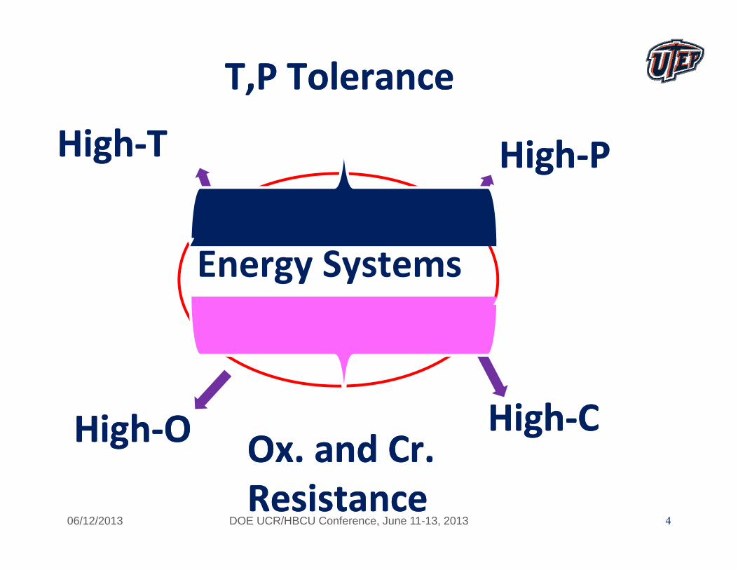
Energy Systems
High‐THigh‐T High‐PHigh‐P
High‐CHigh‐CHigh‐OHigh‐O
T,P ToleranceT,P Tolerance
Ox. and Cr. ResistanceOx. and Cr. Resistance
06/12/2013 DOE UCR/HBCU Conference, June 11-13, 2013
5
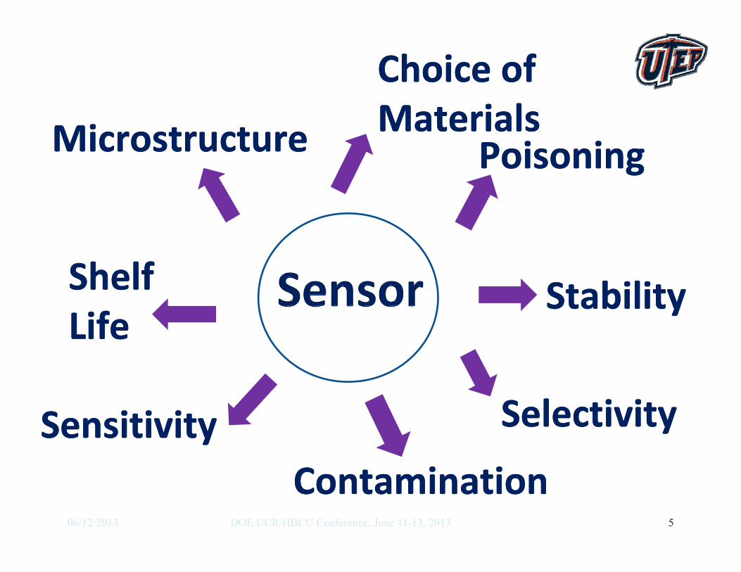
MicrostructureMicrostructure
Choice of MaterialsChoice of Materials
SensitivitySensitivity
PoisoningPoisoning
SelectivitySelectivity
ContaminationContamination
Shelf LifeShelf Life
StabilityStability
06/12/2013 DOE UCR/HBCU Conference, June 11-13, 2013
6
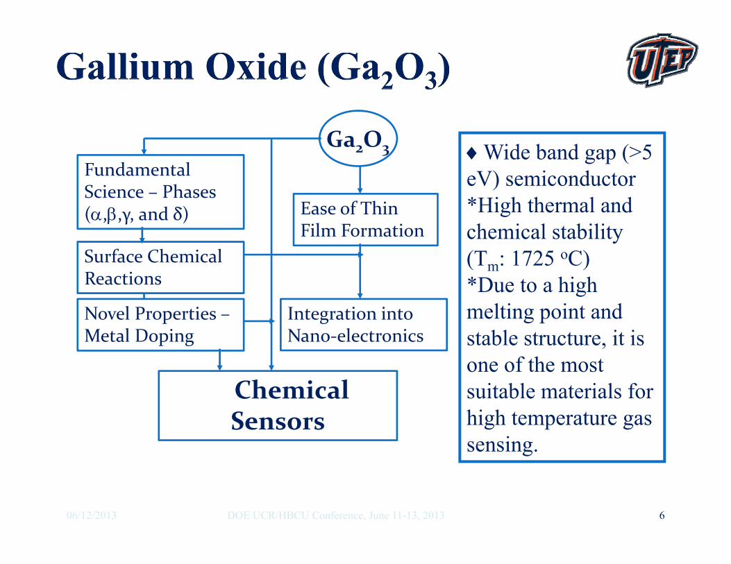
Fundamental Science – Phases (,,γ, and δ)
Novel Properties –Metal Doping
Surface Chemical Reactions
Chemical Sensors
Ease of Thin Film Formation
Integration into Nano‐electronics
Ga2O3 Wide band gap (>5 eV) semiconductor *High thermal and chemical stability (Tm: 1725 oC)*Due to a high melting point and stable structure, it is one of the most suitable materials for high temperature gas sensing.
06/12/2013 DOE UCR/HBCU Conference, June 11-13, 2013
706/12/2013 DOE UCR/HBCU Conference, June 11-13, 2013
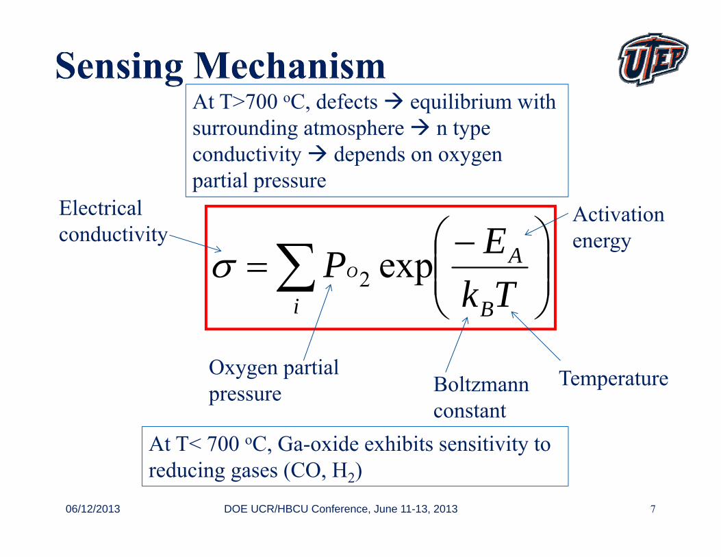
Tk
EPB
A
iO exp2
Activation energy
Oxygen partial pressure Boltzmann
constantTemperature
Electrical conductivity
At T>700 oC, defects equilibrium with surrounding atmosphere n type conductivity depends on oxygen partial pressure
At T< 700 oC, Ga-oxide exhibits sensitivity to reducing gases (CO, H2)
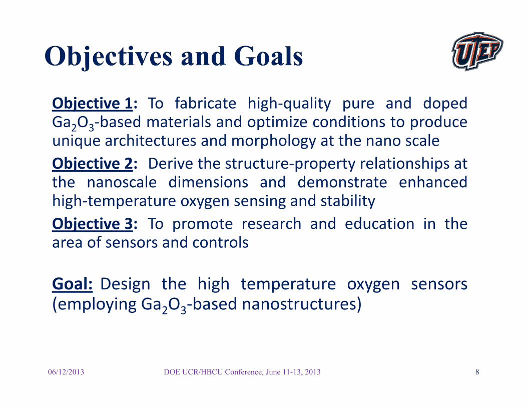
Objective 1: To fabricate high‐quality pure and dopedGa2O3‐based materials and optimize conditions to produceunique architectures and morphology at the nano scaleObjective 2: Derive the structure‐property relationships atthe nanoscale dimensions and demonstrate enhancedhigh‐temperature oxygen sensing and stabilityObjective 3: To promote research and education in thearea of sensors and controls
Goal: Design the high temperature oxygen sensors(employing Ga2O3‐based nanostructures)
806/12/2013 DOE UCR/HBCU Conference, June 11-13, 2013
906/12/2013 DOE UCR/HBCU Conference, June 11-13, 2013
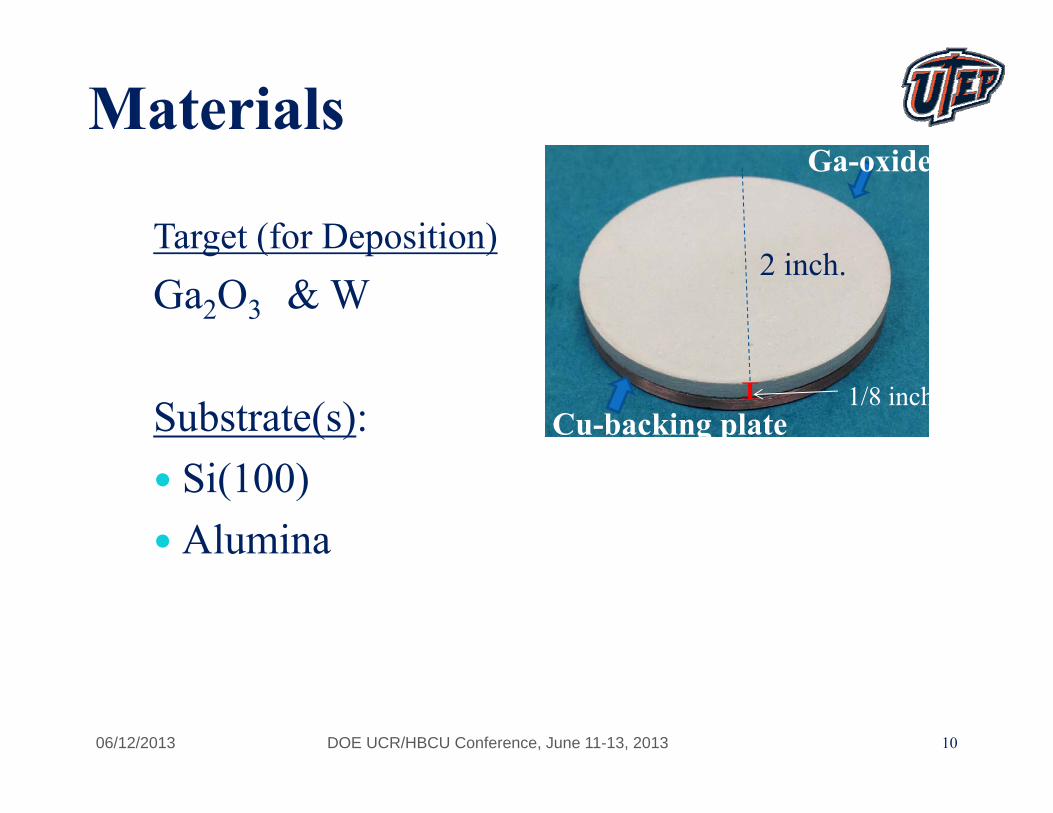
Target (for Deposition)Ga2O3 & W
Substrate(s): Si(100) Alumina
MaterialsGa-oxide
Cu-backing plate
2 inch.
1/8 inch.
1006/12/2013 DOE UCR/HBCU Conference, June 11-13, 2013
11
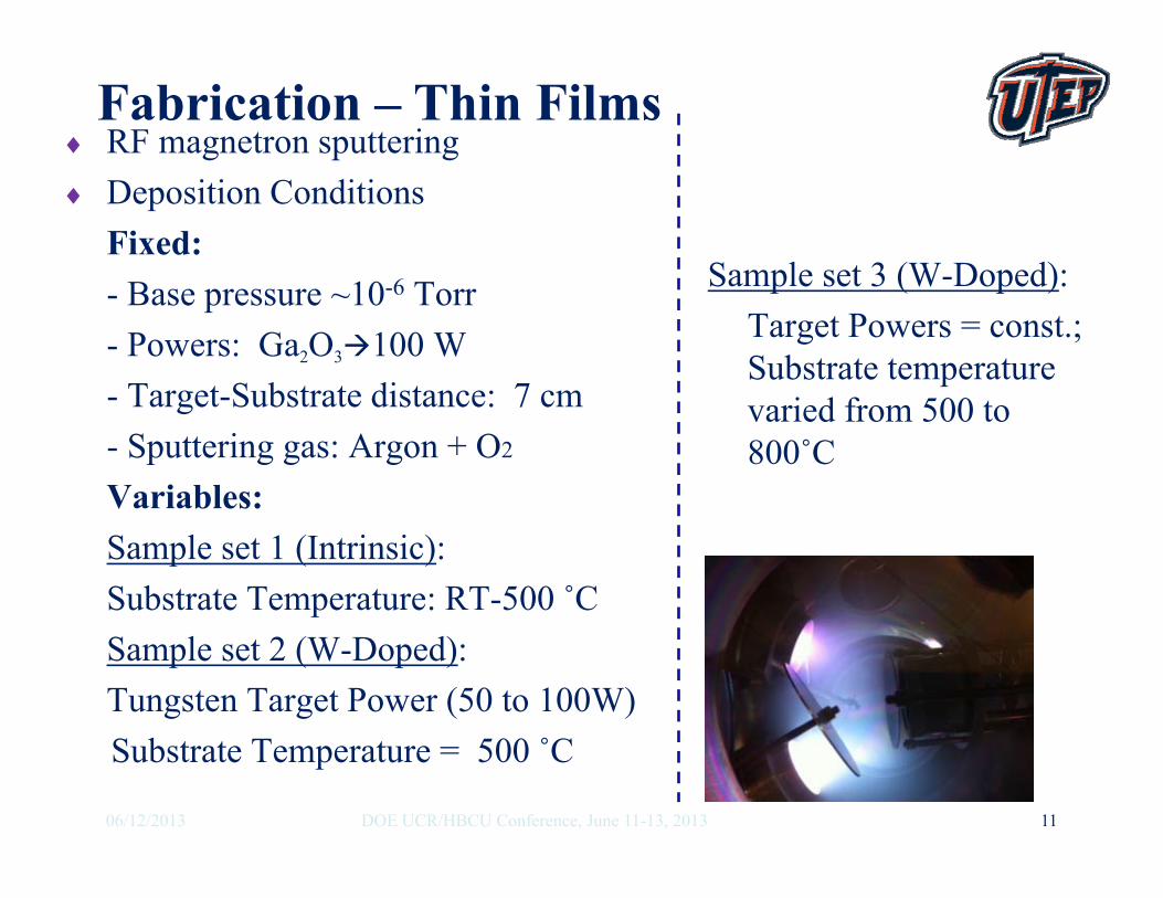
RF magnetron sputtering Deposition Conditions
Fixed:- Base pressure ~10-6 Torr- Powers: Ga2O3100 W- Target-Substrate distance: 7 cm- Sputtering gas: Argon + O2
Variables: Sample set 1 (Intrinsic): Substrate Temperature: RT-500 ˚CSample set 2 (W-Doped): Tungsten Target Power (50 to 100W)Substrate Temperature = 500 ˚C
Fabrication – Thin Films
06/12/2013 DOE UCR/HBCU Conference, June 11-13, 2013
Sample set 3 (W-Doped): Target Powers = const.; Substrate temperature varied from 500 to 800˚C
12
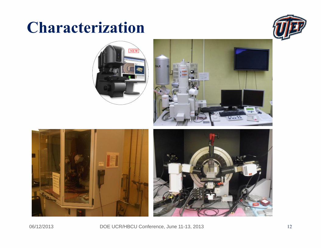
Characterization
06/12/2013 DOE UCR/HBCU Conference, June 11-13, 2013
13
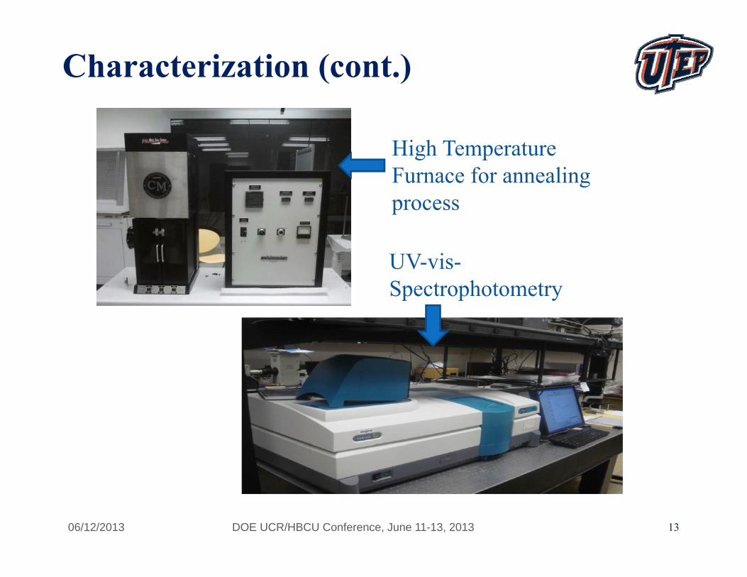
Characterization (cont.)
High Temperature Furnace for annealing process
UV-vis-Spectrophotometry
06/12/2013 DOE UCR/HBCU Conference, June 11-13, 2013
PVD: Sputtering
1406/12/2013 DOE UCR/HBCU Conference, June 11-13, 2013
15
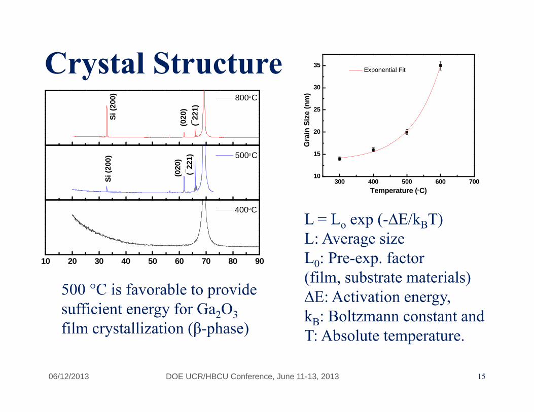
10 20 30 40 50 60 70 80 90
Si (2
00)
Si (2
00)
800C
(020
)(
221)
(020
)(
221)
500C
400C
06/12/2013 DOE UCR/HBCU Conference, June 11-13, 2013
Crystal Structure
300 400 500 600 70010
15
20
25
30
35 Exponential Fit
Gra
in S
ize
(nm
)
Temperature (C)
L = Lo exp (-∆E/kBT)L: Average size L0: Pre-exp. factor (film, substrate materials) ∆E: Activation energy, kB: Boltzmann constant and T: Absolute temperature.
500 °C is favorable to provide sufficient energy for Ga2O3film crystallization (β-phase)
06/12/2013 DOE UCR/HBCU Conference, June 11-13, 2013 16
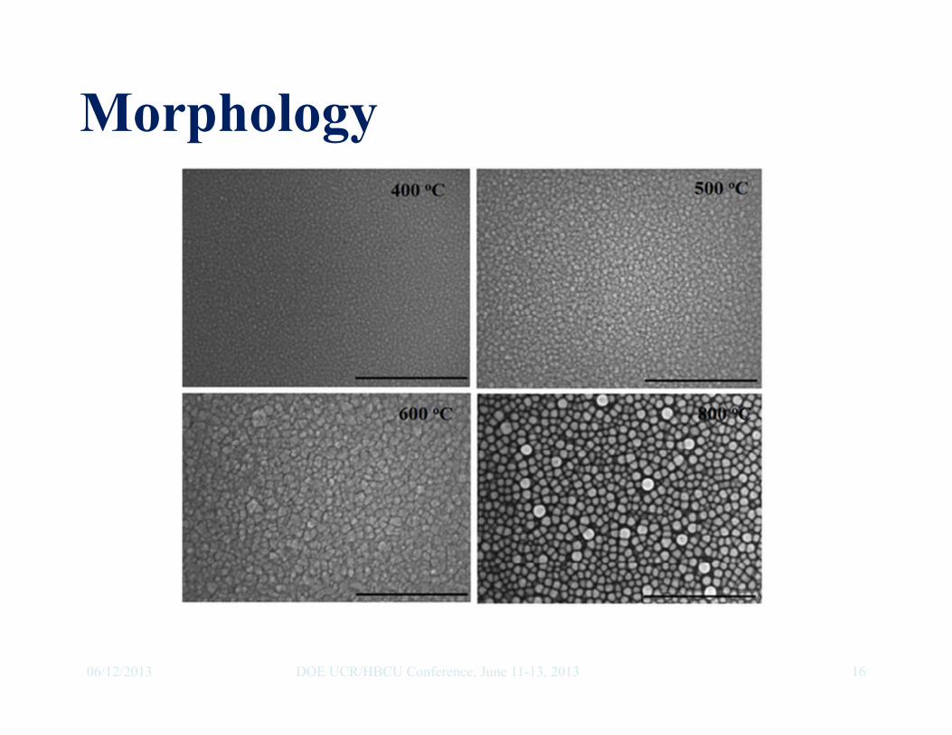
Morphology
1706/12/2013 DOE UCR/HBCU Conference, June 11-13, 2013
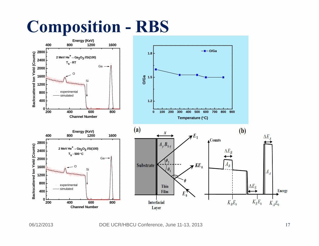
Composition - RBS
200 400 600 8000
400
800
1200
1600
2000
2400
2800
400 800 1200 1600
2 MeV He+ Ga2O3//Si(100)Ts - 600 C
Energy (KeV)
Channel Number
Bac
ksca
ttere
d Io
n Yi
eld
(Cou
nts)
experimental simulated
OGa
Si
200 400 600 8000
400
800
1200
1600
2000
2400
2800
400 800 1200 1600Energy (KeV)
2 MeV He+ Ga2O3 //Si(100)Ts - 500C
Bac
ksca
ttere
d Io
n Yi
eld
(Cou
nts)
Channel Number
experimental simulated
OSi
Ga
200 400 600 8000
400
800
1200
1600
2000
2400
2800
400 800 1200 1600
Channel Number
Bac
ksca
ttere
d Io
n Yi
eld
(Cou
nts)
2 MeV He+ Ga2O3 //Si(100)Ts - 300 C
experimental simulated
Energy (KeV)
O SiGa
200 400 600 8000
400
800
1200
1600
2000
2400
2800
400 800 1200 1600
2 MeV He+ Ga2O3 //Si(100)
Ts - RT
Channel Number
Energy (KeV)
Bac
ksca
ttere
d Io
n Yi
eld
(Cou
nts)
experimental simulated
O
Si
Ga
0 100 200 300 400 500 600 700 800 900
1.2
1.5
1.8
O/G
a
Temperature (C)
O/Ga
1806/12/2013 DOE UCR/HBCU Conference, June 11-13, 2013
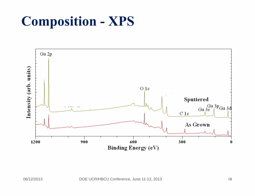
Composition - XPS
06/12/2013 DOE UCR/HBCU Conference, June 11-13, 2013 19
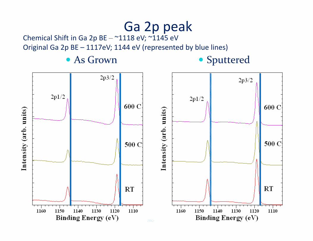
Ga 2p peak
As Grown Sputtered
Chemical Shift in Ga 2p BE – ~1118 eV; ~1145 eVOriginal Ga 2p BE – 1117eV; 1144 eV (represented by blue lines)
2006/12/2013 DOE UCR/HBCU Conference, June 11-13, 2013
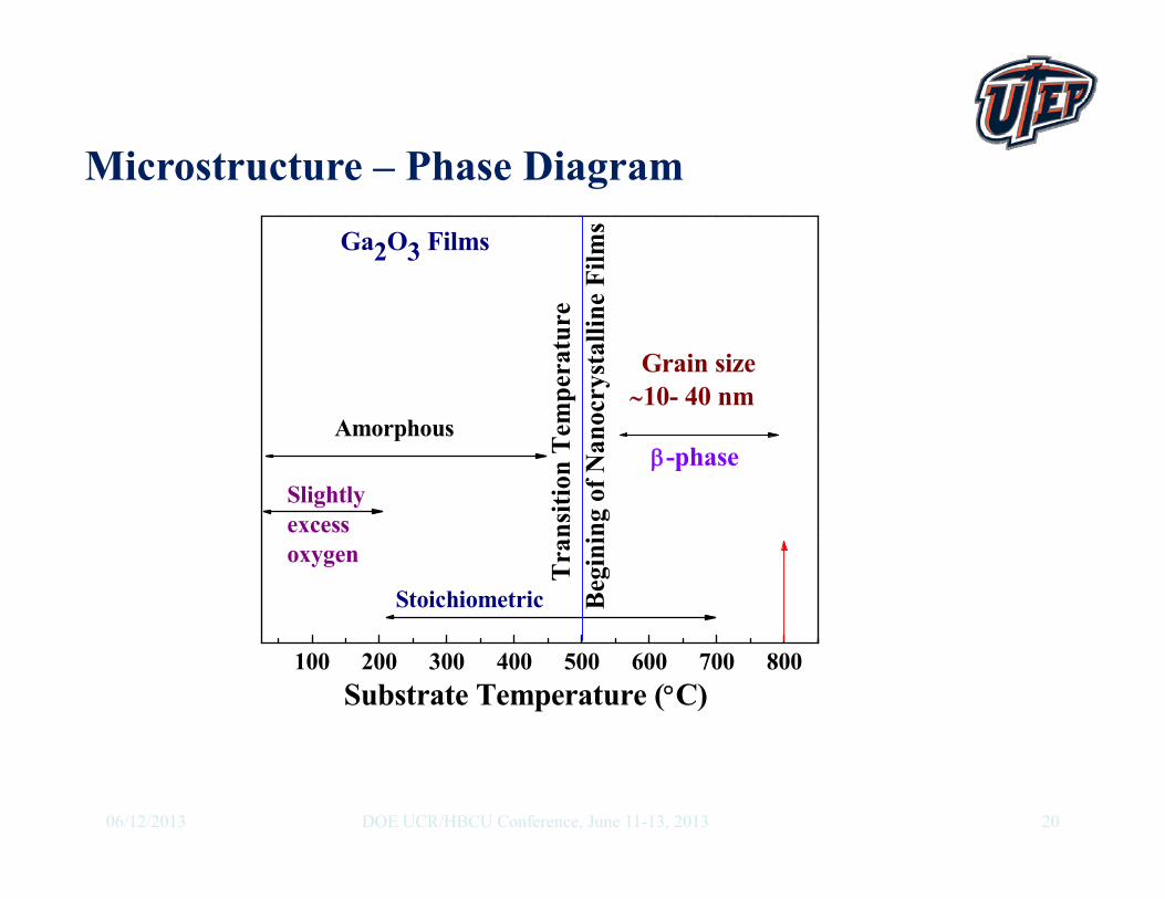
Microstructure – Phase Diagram
100 200 300 400 500 600 700 800
Slightly excess oxygen
Stoichiometric T
rans
ition
Tem
pera
ture
B
egin
ing
of N
anoc
ryst
allin
e Fi
lms
Grain size 10- 40 nm
-phase
Ga2O3 Films
Amorphous
Substrate Temperature (C)
2106/12/2013 DOE UCR/HBCU Conference, June 11-13, 2013
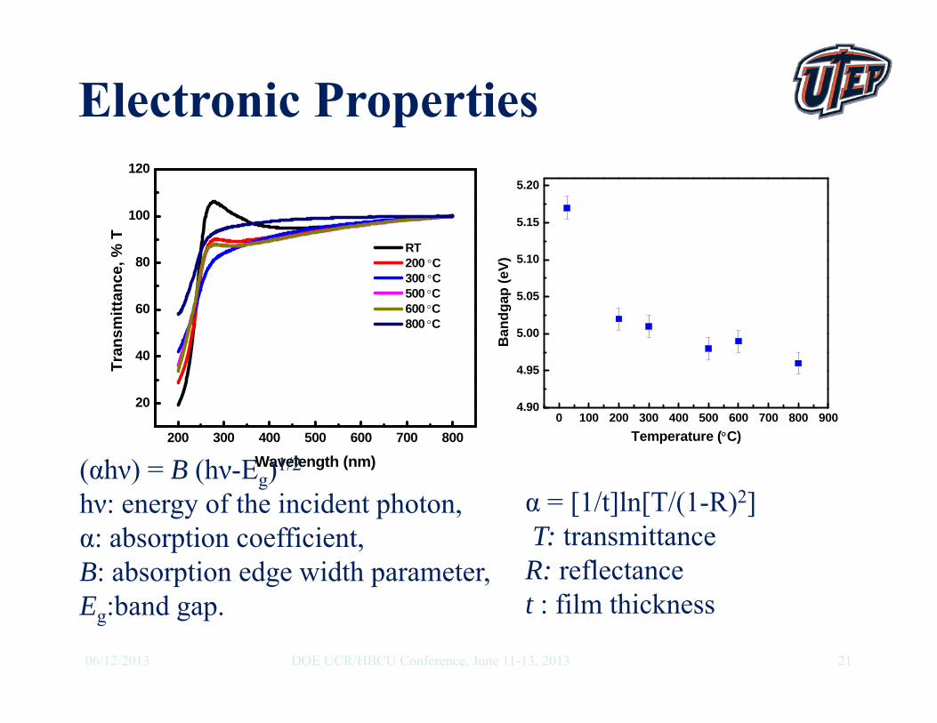
200 300 400 500 600 700 800
20
40
60
80
100
120
Tran
smitt
ance
, % T
Wavelength (nm)
RT 200 C 300 C 500C 600C 800C
0 100 200 300 400 500 600 700 800 9004.90
4.95
5.00
5.05
5.10
5.15
5.20
Ban
dgap
(eV)
Temperature (C)
Electronic Properties
(αhν) = B (hν-Eg)1/2
hν: energy of the incident photon, α: absorption coefficient, B: absorption edge width parameter, Eg:band gap.
α = [1/t]ln[T/(1-R)2]T: transmittance R: reflectance t : film thickness
PVD: Sputtering
2206/12/2013 DOE UCR/HBCU Conference, June 11-13, 2013
200 ̊C
23
300 ̊C
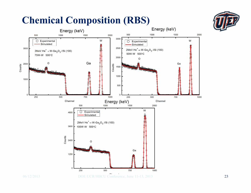
Chemical Composition (RBS)
06/12/2013 DOE UCR/HBCU Conference, June 11-13, 2013
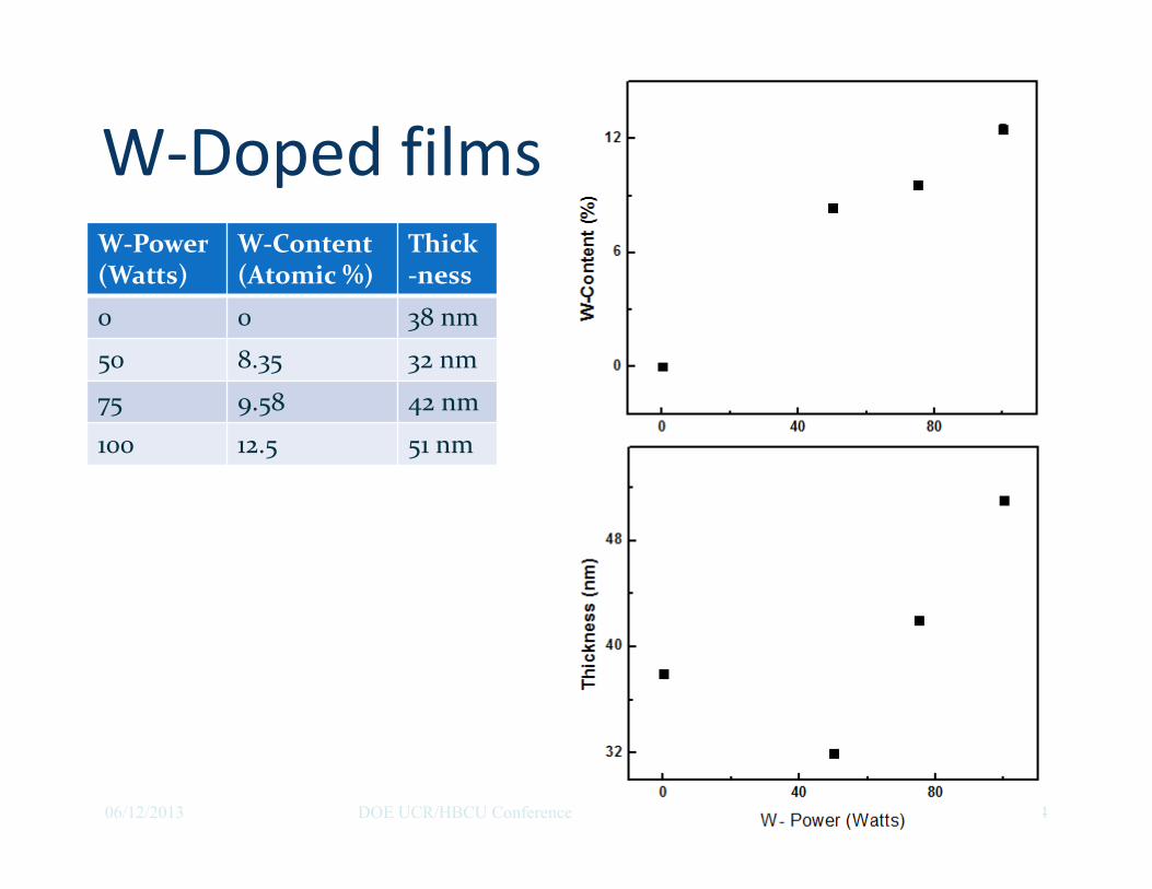
W‐Doped filmsW‐Power (Watts)
W‐Content (Atomic %)
Thick‐ness
0 0 38 nm
50 8.35 32 nm
75 9.58 42 nm
100 12.5 51 nm
06/12/2013 DOE UCR/HBCU Conference, June 11-13, 2013 24
25
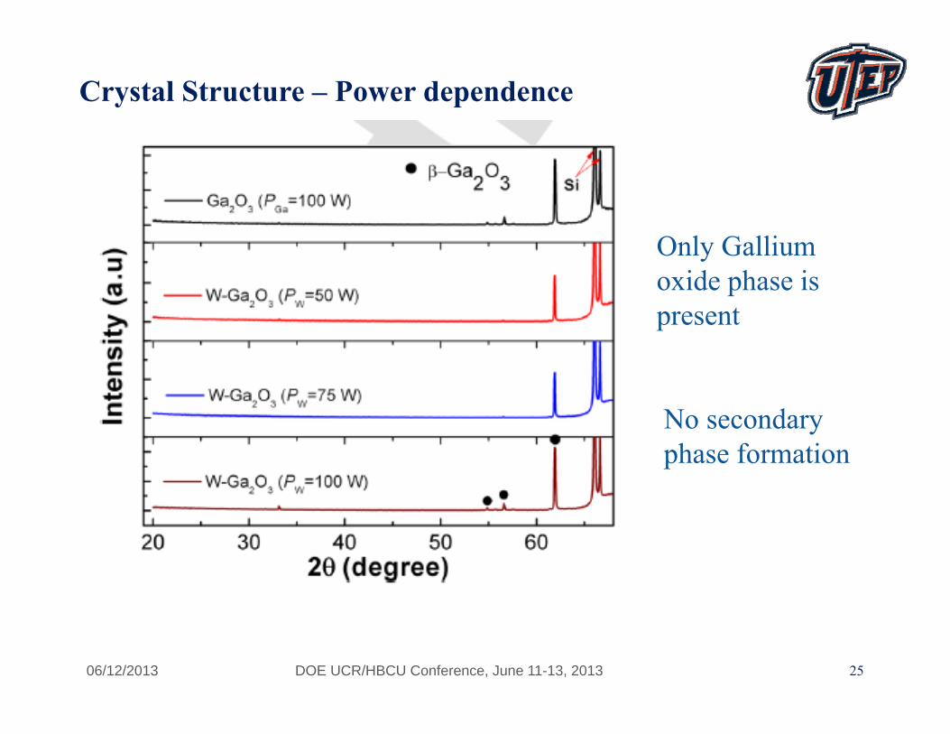
Crystal Structure – Power dependence
Only Gallium oxide phase is present
06/12/2013 DOE UCR/HBCU Conference, June 11-13, 2013
No secondary phase formation
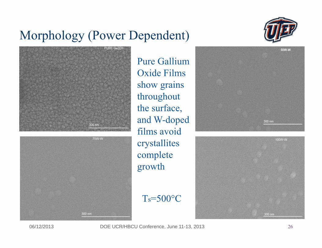
Morphology (Power Dependent)
Pure Gallium Oxide Films show grains throughout the surface, and W-doped films
Pure Gallium Oxide Films show grains throughout the surface, and W-doped films avoid crystallites complete growth
Ts=500°C
2606/12/2013 DOE UCR/HBCU Conference, June 11-13, 2013
27
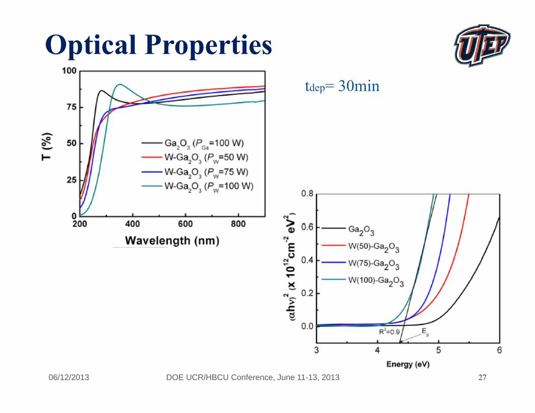
Optical Propertiestdep= 30min
06/12/2013 DOE UCR/HBCU Conference, June 11-13, 2013
28
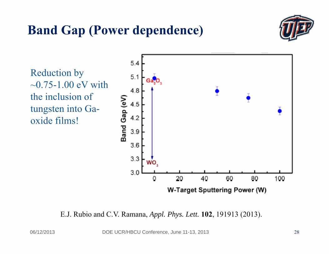
Band Gap (Power dependence)
28
Reduction by ~0.75-1.00 eV with the inclusion of tungsten into Ga-oxide films!
E.J. Rubio and C.V. Ramana, Appl. Phys. Lett. 102, 191913 (2013).
06/12/2013 DOE UCR/HBCU Conference, June 11-13, 2013
29
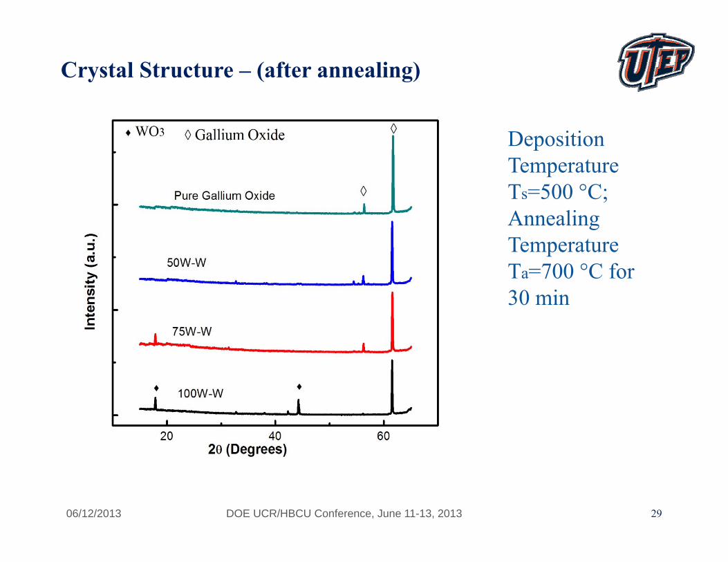
Crystal Structure – (after annealing)
Deposition Temperature Ts=500 °C;Annealing TemperatureTa=700 °C for 30 min
06/12/2013 DOE UCR/HBCU Conference, June 11-13, 2013
30
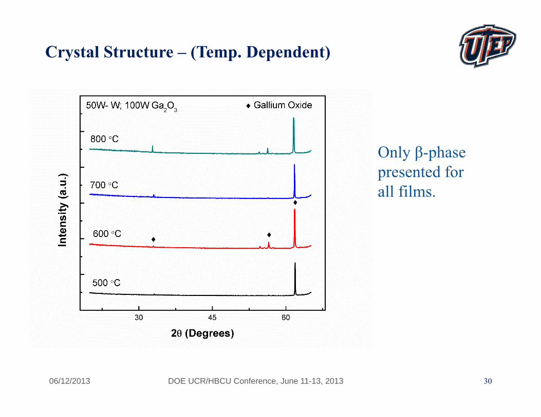
Crystal Structure – (Temp. Dependent)
Only β-phase presented for all films.
06/12/2013 DOE UCR/HBCU Conference, June 11-13, 2013
Morphology – Broad View
31
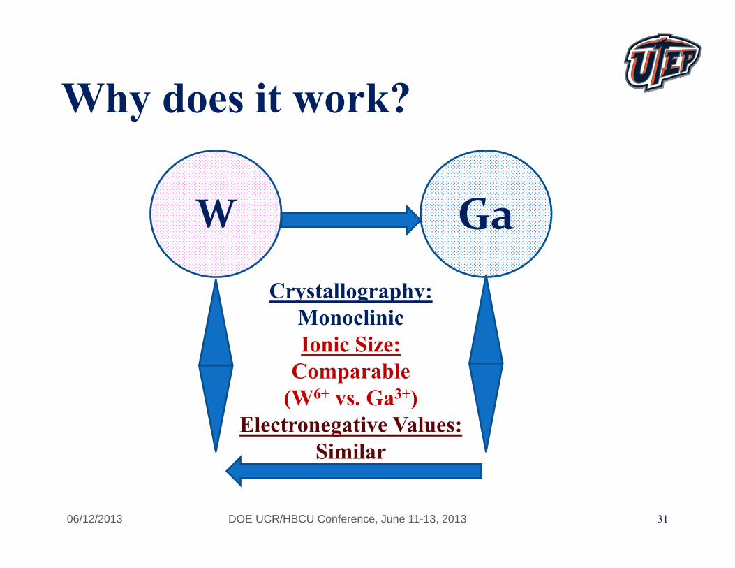
Why does it work?
06/12/2013 DOE UCR/HBCU Conference, June 11-13, 2013
Crystallography: MonoclinicIonic Size:
Comparable (W6+ vs. Ga3+)
Electronegative Values:Similar
W Ga
Morphology – Broad View
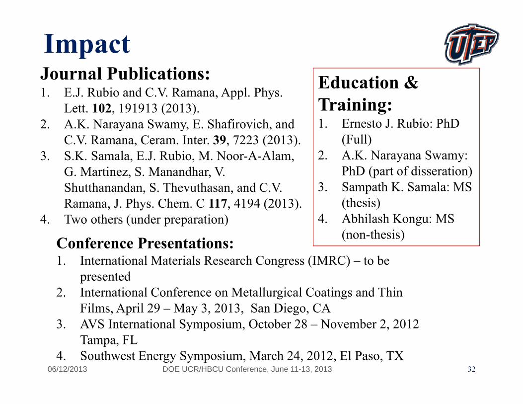
32
ImpactJournal Publications:1. E.J. Rubio and C.V. Ramana, Appl. Phys.
Lett. 102, 191913 (2013).2. A.K. Narayana Swamy, E. Shafirovich, and
C.V. Ramana, Ceram. Inter. 39, 7223 (2013).3. S.K. Samala, E.J. Rubio, M. Noor-A-Alam,
G. Martinez, S. Manandhar, V. Shutthanandan, S. Thevuthasan, and C.V. Ramana, J. Phys. Chem. C 117, 4194 (2013).
4. Two others (under preparation)
Conference Presentations:1. International Materials Research Congress (IMRC) – to be
presented 2. International Conference on Metallurgical Coatings and Thin
Films, April 29 – May 3, 2013, San Diego, CA3. AVS International Symposium, October 28 – November 2, 2012
Tampa, FL4. Southwest Energy Symposium, March 24, 2012, El Paso, TX
Education & Training:1. Ernesto J. Rubio: PhD
(Full)2. A.K. Narayana Swamy:
PhD (part of disseration)3. Sampath K. Samala: MS
(thesis)4. Abhilash Kongu: MS
(non-thesis)
06/12/2013 DOE UCR/HBCU Conference, June 11-13, 2013
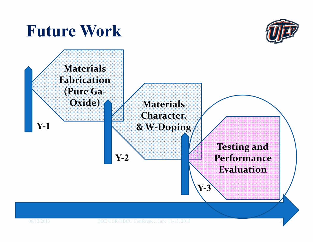
Future Work
06/12/2013 DOE UCR/HBCU Conference, June 11-13, 2013 33
Materials Fabrication(Pure Ga‐Oxide) Materials
Character.& W‐Doping
Testing and Performance Evaluation
Y-1
Y-2
Y-3
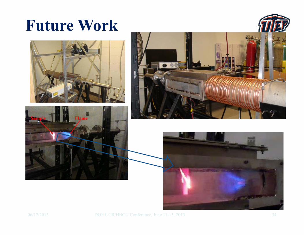
Future Work
06/12/2013 DOE UCR/HBCU Conference, June 11-13, 2013 34
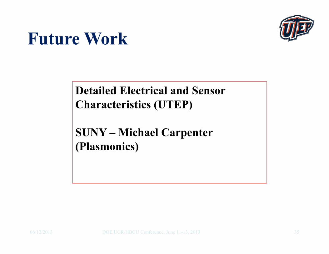
Future Work
06/12/2013 DOE UCR/HBCU Conference, June 11-13, 2013 35
Detailed Electrical and Sensor Characteristics (UTEP)
SUNY – Michael Carpenter (Plasmonics)
36
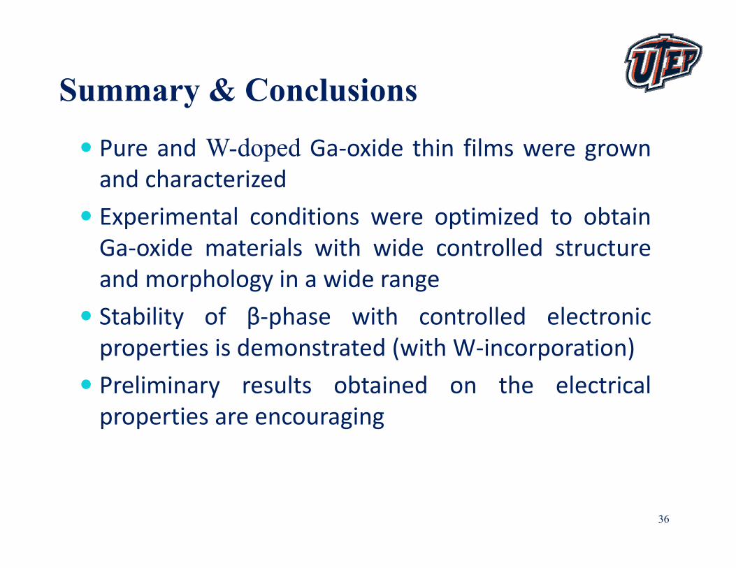
Summary & Conclusions
Pure and W-doped Ga‐oxide thin films were grownand characterized
Experimental conditions were optimized to obtainGa‐oxide materials with wide controlled structureand morphology in a wide range
Stability of β‐phase with controlled electronicproperties is demonstrated (with W‐incorporation)
Preliminary results obtained on the electricalproperties are encouraging
37
AcknowledgementsDOE‐NETLRichard DunstEMSL/PNNL, Richland, WA
10/25/2011 UTSR Workshop, Oct. 25-27, 201106/12/2013 DOE UCR/HBCU Conference, June 11-13, 2013
THANK YOU!