
Gallium Arsenide photocathodes used in high electric...
14
6 mai 1998 CTF Note 98-13 1 Gallium Arsenide photocathodes used in high electric fields Results of experiment from November 1997 to January 1998 Contributors : H. Braun, F. Chautard, E. Chevallay, J. Durand, S. Hutchins, G. Suberlucq (editor), H. Trautner (CERN) J. Clendenin, G. Mulhollan (SLAC) 1. Introduction This paper summarises the work done from November 1997 to January 1998 in the collaboration between SLAC and CERN to test GaAs Photocathodes in the RF gun of the CERN CLIC Test Facility. The interesting property of GaAs is as a source of polarised electrons, for which the optimum wavelength of the illumination is about 850nm. No suitable light source at this wavelength was available, the measurements were made at 532, 266 and 213 nm, at which wavelengths the quantum efficiency is greater, but the electrons produced have very low polarization. The trials concentrate on the procedure to produce GaAs cathodes activated by cesium and oxygen and study their behaviour in the high electric field of the RF gun. 2. Preparation of the Gallium Arsenide Photocathode The Gallium Arsenide (GaAs) samples and the assembly set were supplied by the Stanford Linear Accelerator Centre (SLAC). In this way a GaAs sample can be mounted inside the body of a Photocathode plug used in the RF gun of the CTF drive beam at CERN (fig. 1). The Mo retaining ring was omitted in the final design. Φ = 6 mm Figure 1-a Figure 1-b Two sets of samples were supplied, the first set of four were used to test the assembly and cleaning procedures and for familiarization with the equipment, then a second set of four with precise machining, which could be inserted into the CTF source without detuning the RF cavity. 2.1. Chemical cleaning The GaAs sample is protected by an anodized surface which must be removed before mounting. The SLAC Anodisation Removal Procedure was followed : Immersion for thirty seconds in Ammonia hydroxide (NH 4 OH), rinsing with a steady stream of deionised water (H 2 O), followed by a rinse in a steady stream of methanol (CH 3 OH) and finally blown dry with Nitrogen (N 2 ). The pictures 2a, 2b show the GaAs photocathode ready to be placed in the preparation chamber. deionised water (H 2 O), followed by a rinse in a steady stream of methanol (CH 3 OH) and finally blown dry with Nitrogen (N 2 ). The pictures 2a, 2b show the GaAs photocathode ready to be placed in the preparation chamber.
Transcript of Gallium Arsenide photocathodes used in high electric...

6 mai 1998 CTF Note 98-13
1
Gallium Arsenide photocathodes used in high electric fieldsResults of experiment from November 1997 to January 1998
Contributors : H. Braun, F. Chautard, E. Chevallay, J. Durand, S. Hutchins, G. Suberlucq (editor), H. Trautner (CERN)J. Clendenin, G. Mulhollan (SLAC)
1. IntroductionThis paper summarises the work done from November 1997 to January 1998 in the collaboration between SLAC andCERN to test GaAs Photocathodes in the RF gun of the CERN CLIC Test Facility. The interesting property of GaAs is asa source of polarised electrons, for which the optimum wavelength of the illumination is about 850nm. No suitable lightsource at this wavelength was available, the measurements were made at 532, 266 and 213 nm, at which wavelengths thequantum efficiency is greater, but the electrons produced have very low polarization. The trials concentrate on theprocedure to produce GaAs cathodes activated by cesium and oxygen and study their behaviour in the high electric field ofthe RF gun.
2. Preparation of the Gallium Arsenide PhotocathodeThe Gallium Arsenide (GaAs) samples and the assembly set were supplied by the Stanford Linear Accelerator Centre(SLAC). In this way a GaAs sample can be mounted inside the body of a Photocathode plug used in the RF gun of the CTFdrive beam at CERN (fig. 1). The Mo retaining ring was omitted in the final design.
Φ = 6 mm
Figure 1-a Figure 1-b
Two sets of samples were supplied, the first set of four were used to test the assembly and cleaning procedures and forfamiliarization with the equipment, then a second set of four with precise machining, which could be inserted into theCTF source without detuning the RF cavity.
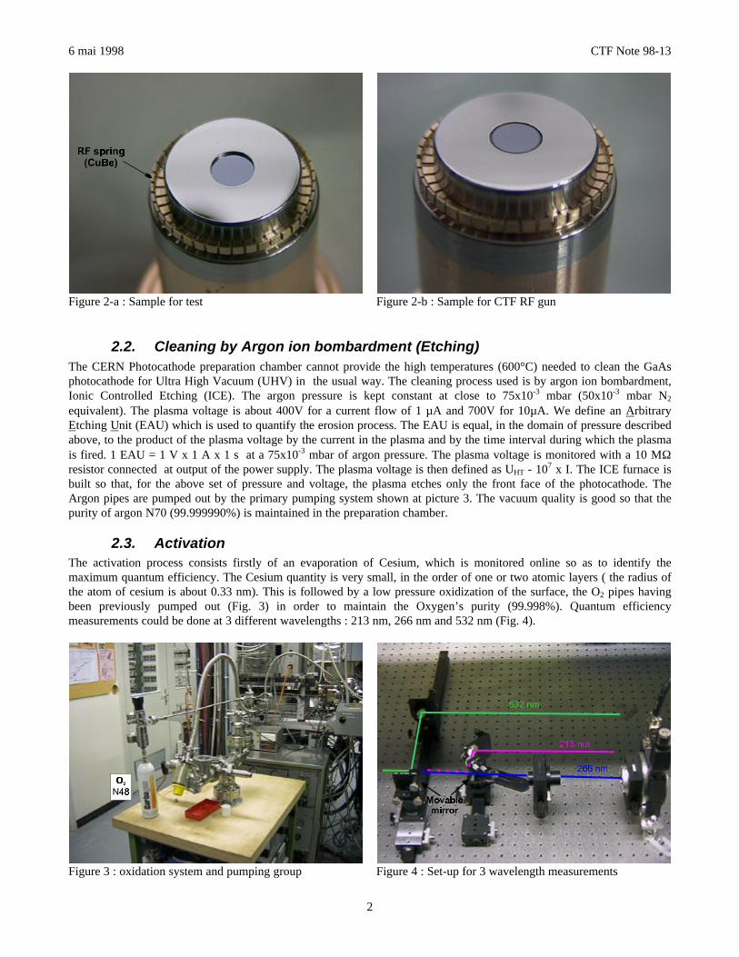
2.1. Chemical cleaningThe GaAs sample is protected by an anodized surface which must be removed before mounting. The SLAC AnodisationRemoval Procedure was followed : Immersion for thirty seconds in Ammonia hydroxide (NH4OH), rinsing with a steadystream of deionised water (H2O), followed by a rinse in a steady stream of methanol (CH3OH) and finally blown dry withNitrogen (N2). The pictures 2a, 2b show the GaAs photocathode ready to be placed in the preparation chamber.deionised water (H2O), followed by a rinse in a steady stream of methanol (CH3OH) and finally blown dry with Nitrogen(N2). The pictures 2a, 2b show the GaAs photocathode ready to be placed in the preparation chamber.
6 mai 1998 CTF Note 98-13
2
Figure 2-a : Sample for test Figure 2-b : Sample for CTF RF gun
2.2. Cleaning by Argon ion bombardment (Etching)The CERN Photocathode preparation chamber cannot provide the high temperatures (600°C) needed to clean the GaAsphotocathode for Ultra High Vacuum (UHV) in the usual way. The cleaning process used is by argon ion bombardment,Ionic Controlled Etching (ICE). The argon pressure is kept constant at close to 75x10-3 mbar (50x10-3 mbar N2
equivalent). The plasma voltage is about 400V for a current flow of 1 µA and 700V for 10µA. We define an ArbitraryEtching Unit (EAU) which is used to quantify the erosion process. The EAU is equal, in the domain of pressure describedabove, to the product of the plasma voltage by the current in the plasma and by the time interval during which the plasmais fired. 1 EAU = 1 V x 1 A x 1 s at a 75x10-3 mbar of argon pressure. The plasma voltage is monitored with a 10 MΩresistor connected at output of the power supply. The plasma voltage is then defined as UHT - 107 x I. The ICE furnace isbuilt so that, for the above set of pressure and voltage, the plasma etches only the front face of the photocathode. TheArgon pipes are pumped out by the primary pumping system shown at picture 3. The vacuum quality is good so that thepurity of argon N70 (99.999990%) is maintained in the preparation chamber.
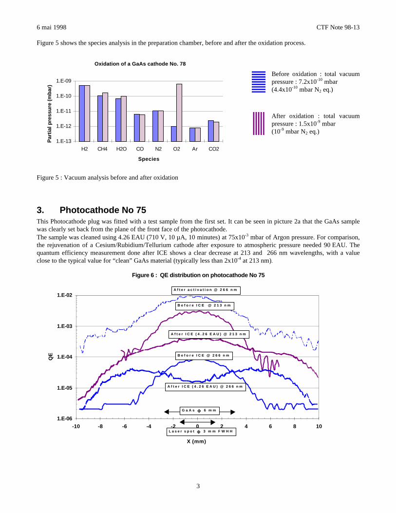
2.3. ActivationThe activation process consists firstly of an evaporation of Cesium, which is monitored online so as to identify themaximum quantum efficiency. The Cesium quantity is very small, in the order of one or two atomic layers ( the radius ofthe atom of cesium is about 0.33 nm). This is followed by a low pressure oxidization of the surface, the O2 pipes havingbeen previously pumped out (Fig. 3) in order to maintain the Oxygen’s purity (99.998%). Quantum efficiencymeasurements could be done at 3 different wavelengths : 213 nm, 266 nm and 532 nm (Fig. 4).
Figure 3 : oxidation system and pumping group Figure 4 : Set-up for 3 wavelength measurements
6 mai 1998 CTF Note 98-13
3
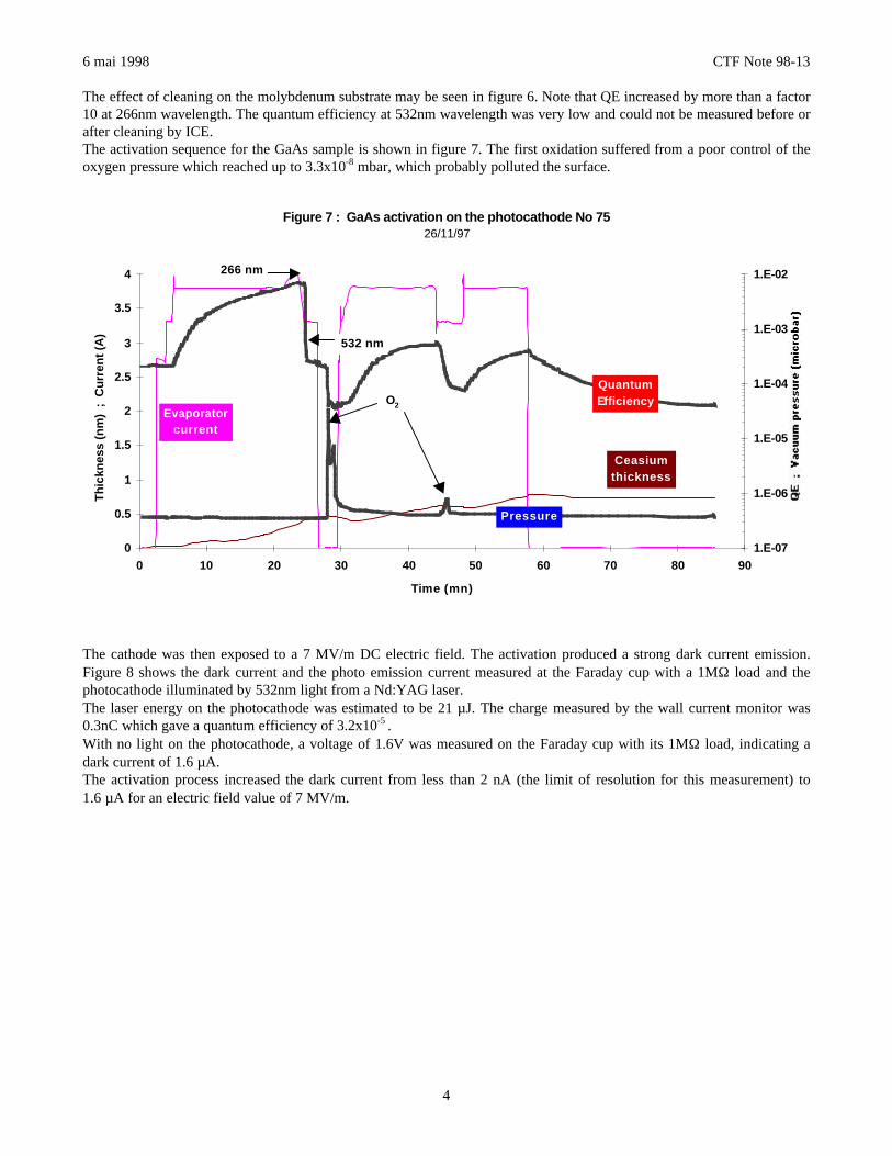
Figure 5 shows the species analysis in the preparation chamber, before and after the oxidation process.
Oxidation of a GaAs cathode No. 78
1.E-13
1.E-12
1.E-11
1.E-10
1.E-09
H2 CH4 H2O CO N2 O2 Ar CO2
Species
Par
tial
pre
ssu
re (
mb
ar)
Before oxidation : total vacuumpressure : 7.2x10⁻¹⁰ mbar(4.4x10⁻¹⁰ mbar N2 eq.)
After oxidation : total vacuumpressure : 1.5x10⁻⁹ mbar(10-9 mbar N2 eq.)
Figure 5 : Vacuum analysis before and after oxidation
3. Photocathode No 75This Photocathode plug was fitted with a test sample from the first set. It can be seen in picture 2a that the GaAs samplewas clearly set back from the plane of the front face of the photocathode.The sample was cleaned using 4.26 EAU (710 V, 10 µA, 10 minutes) at 75x10-3 mbar of Argon pressure. For comparison,the rejuvenation of a Cesium/Rubidium/Tellurium cathode after exposure to atmospheric pressure needed 90 EAU. Thequantum efficiency measurement done after ICE shows a clear decrease at 213 and 266 nm wavelengths, with a valueclose to the typical value for “clean” GaAs material (typically less than 2x10⁻⁴ at 213 nm).
Figure 6 : QE distribution on photocathode No 75
1.E-06
1.E-05
1.E-04
1.E-03
1.E-02
-10 -8 -6 -4 -2 0 2 4 6 8 10
X (mm)
QE
B e f o r e I C E @ 2 1 3 n m
B e f o r e I C E @ 2 6 6 n m
A f t e r I C E ( 4 . 2 6 E A U ) @ 2 6 6 n m
A f t e r I C E ( 4 . 2 6 E A U ) @ 2 1 3 n m
G a A s ΦΦ 6 m m
L a s e r s p o t ΦΦ 3 m m F W H H
A f t e r a c t i v a t i o n @ 2 6 6 n m
6 mai 1998 CTF Note 98-13
4
The effect of cleaning on the molybdenum substrate may be seen in figure 6. Note that QE increased by more than a factor10 at 266nm wavelength. The quantum efficiency at 532nm wavelength was very low and could not be measured before orafter cleaning by ICE.The activation sequence for the GaAs sample is shown in figure 7. The first oxidation suffered from a poor control of theoxygen pressure which reached up to 3.3x10⁻⁸ mbar, which probably polluted the surface.
Figure 7 : GaAs activation on the photocathode No 7526/11/97
0
0.5
1
1.5
2
2.5
3
3.5
4
0 10 20 30 40 50 60 70 80 90
Time (mn)
Th
ickn
ess
(nm
) ;
Cu
rren
t (A
)
1.E-07
1.E-06
1.E-05
1.E-04
1.E-03
1.E-02266 nm
532 nm
O2
Ceasiumthickness
QuantumEfficiency
Pressure
Evaporatorcurrent
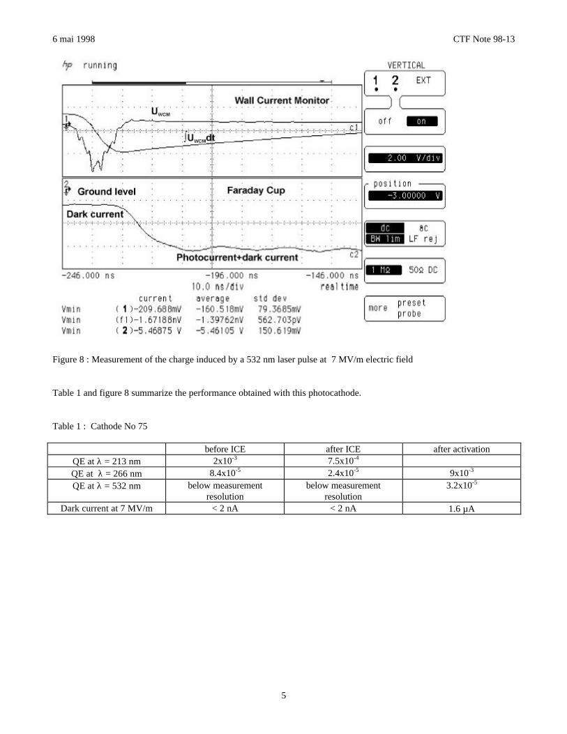
The cathode was then exposed to a 7 MV/m DC electric field. The activation produced a strong dark current emission.Figure 8 shows the dark current and the photo emission current measured at the Faraday cup with a 1MΩ load and thephotocathode illuminated by 532nm light from a Nd:YAG laser.The laser energy on the photocathode was estimated to be 21 µJ. The charge measured by the wall current monitor was0.3nC which gave a quantum efficiency of 3.2x10⁻⁵ .With no light on the photocathode, a voltage of 1.6V was measured on the Faraday cup with its 1MΩ load, indicating adark current of 1.6 µA.The activation process increased the dark current from less than 2 nA (the limit of resolution for this measurement) to1.6 µA for an electric field value of 7 MV/m.
6 mai 1998 CTF Note 98-13
5
Figure 8 : Measurement of the charge induced by a 532 nm laser pulse at 7 MV/m electric field
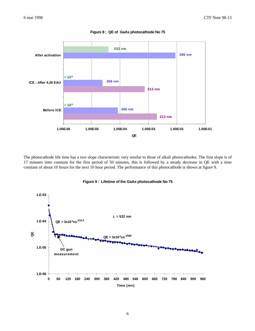
Table 1 and figure 8 summarize the performance obtained with this photocathode.
Table 1 : Cathode No 75
before ICE after ICE after activationQE at λ = 213 nm 2x10⁻³ 7.5x10⁻⁴
QE at λ = 266 nm 8.4x10⁻⁵ 2.4x10⁻⁵ 9x10⁻³
QE at λ = 532 nm below measurementresolution
below measurementresolution
3.2x10⁻⁵
Dark current at 7 MV/m < 2 nA < 2 nA 1.6 µA
6 mai 1998 CTF Note 98-13
6
Figure 8 : QE of GaAs photocathode No 75
1.00E-06 1.00E-05 1.00E-04 1.00E-03 1.00E-02 1.00E-01
Before ICE
ICE : After 4.26 EAU
After activation
QE
< 10-8
< 10-8
532 nm
266 nm
266 nm
266 nm
213 nm
213 nm
The photocathode life time has a two slope characteristic very similar to those of alkali photocathodes. The first slope is of17 minutes time constant for the first period of 50 minutes, this is followed by a steady decrease in QE with a timeconstant of about 10 hours for the next 10 hour period. The performance of this photocathode is shown at figure 9.
Figure 9 : Lifetime of the GaAs photocathode No 75
1.E-06
1.E-05
1.E-04
1.E-03
0 60 120 180 240 300 360 420 480 540 600 660 720 780 840 900 960
Time (mn)
QE
QE = 3x10⁻⁵xe-t/588
QE = 3x10⁻⁴xe-t/16.5λλ = 532 nm
DC gunmeasurement
6 mai 1998 CTF Note 98-13
7
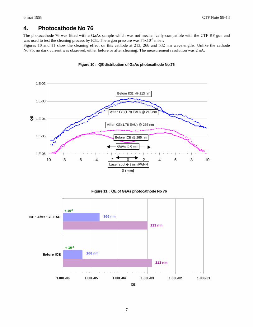
4. Photocathode No 76The photocathode 76 was fitted with a GaAs sample which was not mechanically compatible with the CTF RF gun andwas used to test the cleaning process by ICE. The argon pressure was 75x10-3 mbar.Figures 10 and 11 show the cleaning effect on this cathode at 213, 266 and 532 nm wavelengths. Unlike the cathodeNo 75, no dark current was observed, either before or after cleaning. The measurement resolution was 2 nA.
Figure 10 : QE distribution of GaAs photocathode No.76
1.E-06
1.E-05
1.E-04
1.E-03
1.E-02
-10 -8 -6 -4 -2 0 2 4 6 8 10
X (mm)
QE
Before ICE @ 213 nm
Before ICE @ 266 nm
After ICE (1.78 EAU) @ 266 nm
After ICE (1.78 EAU) @ 213 nm
GaAs Φ 6 mm
Laser spot Φ 3 mm FWHH
Figure 11 : QE of GaAs photocathode No 76
1.00E-06 1.00E-05 1.00E-04 1.00E-03 1.00E-02 1.00E-01
Before ICE
ICE : After 1.78 EAU
QE
< 10-8
< 10-8
266 nm
266 nm
213 nm
213 nm
6 mai 1998 CTF Note 98-13
8
5. Photocathode No 77This cathode was compatible with the CTF RF gun. Unfortunately, after two ICE cleaning cycles, the cathode plugbecame blocked in the clamp of the transfer arm. The preparation chamber had to be returned to atmospheric pressure tofix the mechanical blockage and also to change the scratched photocathode copper plug which was the origin of theproblem.
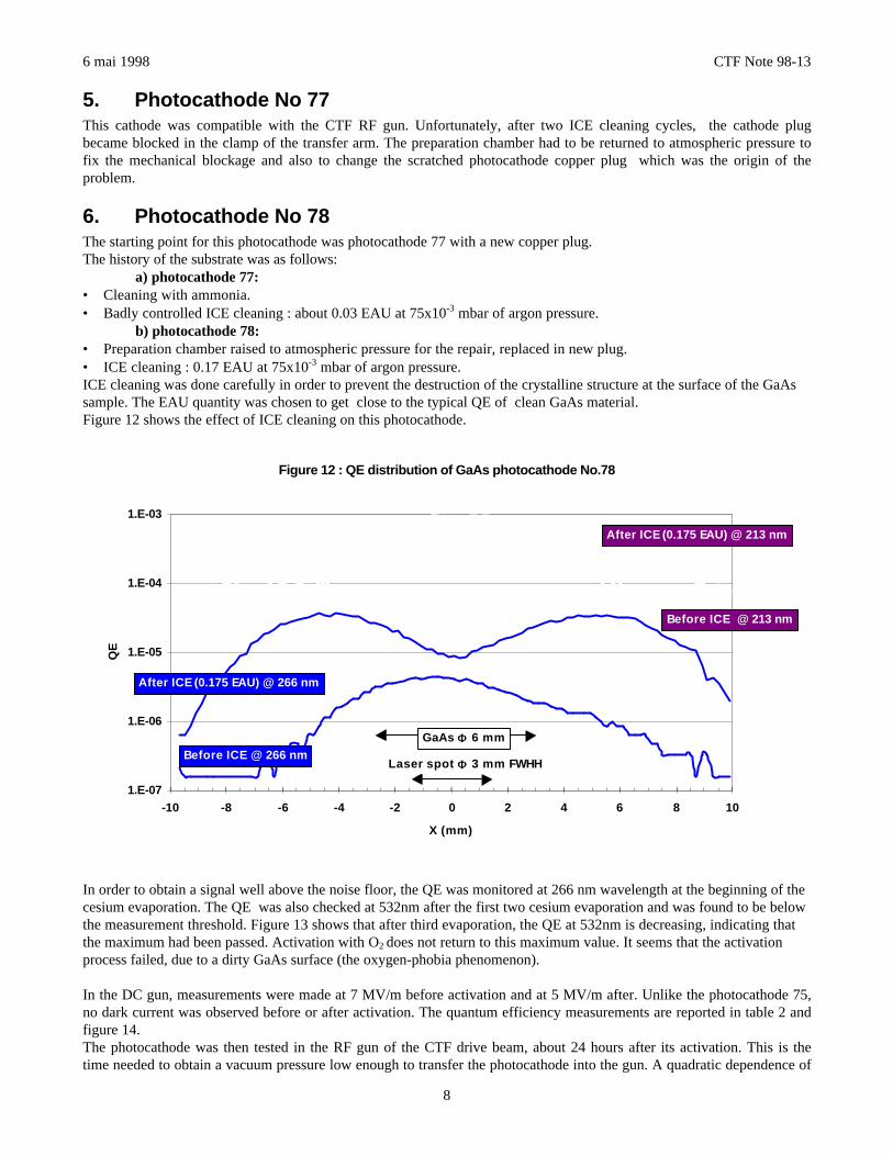
6. Photocathode No 78The starting point for this photocathode was photocathode 77 with a new copper plug.The history of the substrate was as follows:
a) photocathode 77:• Cleaning with ammonia.• Badly controlled ICE cleaning : about 0.03 EAU at 75x10-3 mbar of argon pressure.
b) photocathode 78:• Preparation chamber raised to atmospheric pressure for the repair, replaced in new plug.• ICE cleaning : 0.17 EAU at 75x10-3 mbar of argon pressure.ICE cleaning was done carefully in order to prevent the destruction of the crystalline structure at the surface of the GaAssample. The EAU quantity was chosen to get close to the typical QE of clean GaAs material.Figure 12 shows the effect of ICE cleaning on this photocathode.
Figure 12 : QE distribution of GaAs photocathode No.78
1.E-07
1.E-06
1.E-05
1.E-04
1.E-03
-10 -8 -6 -4 -2 0 2 4 6 8 10
X (mm)
QE
Before ICE @ 213 nm
Before ICE @ 266 nm
After ICE (0.175 EAU) @ 266 nm
GaAs ΦΦ 6 mm
Laser spot ΦΦ 3 mm FWHH
After ICE (0.175 EAU) @ 213 nm
In order to obtain a signal well above the noise floor, the QE was monitored at 266 nm wavelength at the beginning of thecesium evaporation. The QE was also checked at 532nm after the first two cesium evaporation and was found to be belowthe measurement threshold. Figure 13 shows that after third evaporation, the QE at 532nm is decreasing, indicating thatthe maximum had been passed. Activation with O2 does not return to this maximum value. It seems that the activationprocess failed, due to a dirty GaAs surface (the oxygen-phobia phenomenon).
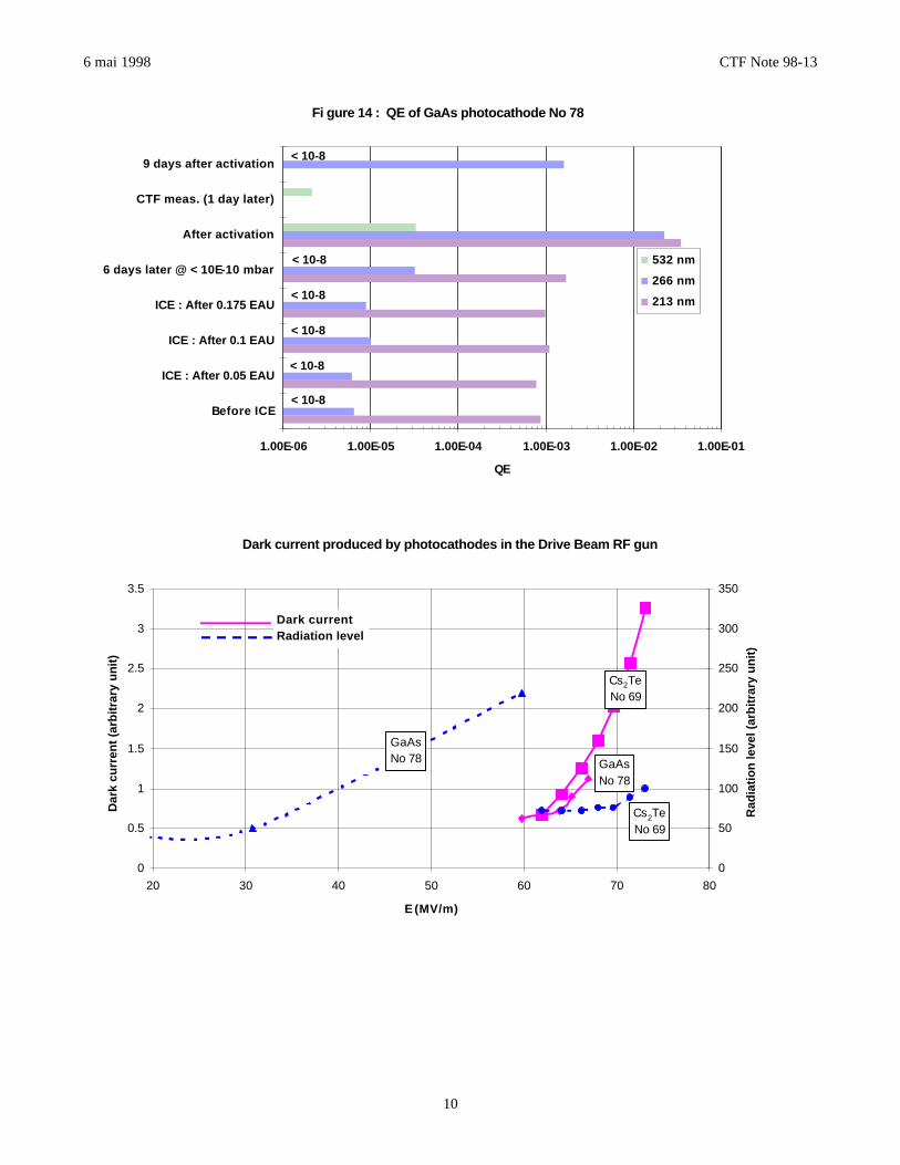
In the DC gun, measurements were made at 7 MV/m before activation and at 5 MV/m after. Unlike the photocathode 75,no dark current was observed before or after activation. The quantum efficiency measurements are reported in table 2 andfigure 14.The photocathode was then tested in the RF gun of the CTF drive beam, about 24 hours after its activation. This is thetime needed to obtain a vacuum pressure low enough to transfer the photocathode into the gun. A quadratic dependence of

6 mai 1998 CTF Note 98-13
9
the emitted charge versus the laser energy was observed, which suggests two photon emission and therefore a workfunction greater than 4.6eV. A slight dependence of the quantum efficiency with the electric field was observed. As withthe DC gun the dark current was very low, its value was lower than that of a Cs2Te photocathode measured a few minutesbefore for comparison purposes. This is again an indication of a high work function and of the failure of the activationprocess. However the radiation generated by the gun with the GaAs photocathode 78 is higher than that of the Cs2Tephotocathode used for comparison (figure 15). All other parameters being supposed similar, this measurement seems tocontradict the dark current measurement. For these measurements, the RF gun was the only load receiving 3 GHz RFpower, and was therefore the only possible source of this radiation.
Figure 13 : Activation of GaAs photocathode No 788/12/1997
0
0.1
0.2
0.3
0.4
0.5
0.6
0 10 20 30 40 50 60 70 80 90 100
Time (mn)
Cae
siu
m t
hic
knes
s (n
m)
0.1x
Eva
po
rato
r p
ow
er (
w)
1.E-06
1.E-05
1.E-04
1.E-03
1.E-02
1.E-01
Vac
uu
m p
ress
ure
(n
bar
) ;
QE
266 nm 532 nm
C a e s i u m
t h i c k n e s s QE
P r e s s u r e
E v a p o r a t o r
P o w e r
O2
Table1 : cathode No 78The DC gun measurements at 5 MV/m. At this level the dark current was below 2 nA.
QE à λ = 213 nm QE à λ = 266 nm QE à λ = 532 nmBefore ICE 9x10⁻⁴ 6.4x10⁻⁶ < 10-8
ICE : 0.05 EAU 7.7x10⁻⁴ 6x10⁻⁶ < 10-8
ICE : 0.1 EAU 1.1x10⁻³ 10-5 < 10-8
ICE : 0.175 EAU 9.8x10⁻⁴ 8.8x10⁻⁶ < 10-8
6 days later a) 1.73x10⁻³ 3.2x10⁻⁵ < 10-8
After activation b) 3.48x10⁻² 2.3x10⁻² 3.3x10⁻⁵
CTF @ 73 MV/m c) 2.1x10⁻⁶ (2 photon effect)9 days later 1.6x10⁻³ < 10-8
a) The photocathode was kept in a vacuum pressure better than 10-10 mbarb) Deposition of 0.54 nm of cesium , then oxidation at about 10-9 mbar oxygen pressurec) About 24 hours after cathode activation
6 mai 1998 CTF Note 98-13
10
Fi gure 14 : QE of GaAs photocathode No 78
1.00E-06 1.00E-05 1.00E-04 1.00E-03 1.00E-02 1.00E-01
Before ICE
ICE : After 0.05 EAU
ICE : After 0.1 EAU
ICE : After 0.175 EAU
6 days later @ < 10E-10 mbar
After activation
CTF meas. (1 day later)
9 days after activation
QE
532 nm
266 nm
213 nm
< 10-8
< 10-8
< 10-8
< 10-8
< 10-8
< 10-8
Dark current produced by photocathodes in the Drive Beam RF gun
0
0.5
1
1.5
2
2.5
3
3.5
20 30 40 50 60 70 80
E (MV/m)
Dar
k cu
rren
t (a
rbit
rary
un
it)
0
50
100
150
200
250
300
350
Rad
iati
on
leve
l (ar
bit
rary
un
it)
Cs2TeNo 69
GaAsNo 78
GaAsNo 78
Cs2TeNo 69
Dark currentRadiation level
6 mai 1998 CTF Note 98-13
11
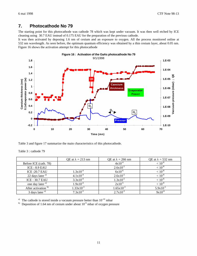
7. Photocathode No 79The starting point for this photocathode was cathode 78 which was kept under vacuum. It was then well etched by ICEcleaning using 30.7 EAU instead of 0.175 EAU for the preparation of the previous cathode.It was then activated by deposing 1.6 nm of cesium and an exposure to oxygen. All the process monitored online at532 nm wavelength. As seen before, the optimum quantum efficiency was obtained by a thin cesium layer, about 0.05 nm.Figure 16 shows the activation attempt for this photocathode
Figure 16 : Activation of the GaAs photocathode No 799/1/1998
-0.2
0
0.2
0.4
0.6
0.8
1
1.2
1.4
1.6
1.8
0 10 20 30 40 50 60 70
Time (mn)
Cae
siu
m t
hic
knes
s (n
m)
0.1x
Eva
po
rato
r p
ow
er (
w)
1.E-10
1.E-09
1.E-08
1.E-07
1.E-06
1.E-05
1.E-04
1.E-03
Vac
cuu
m p
ress
ure
(m
bar
) ;
QE
Caesiumthickness
Pressure
EvaporatorPower
QE
O2
O2 O2
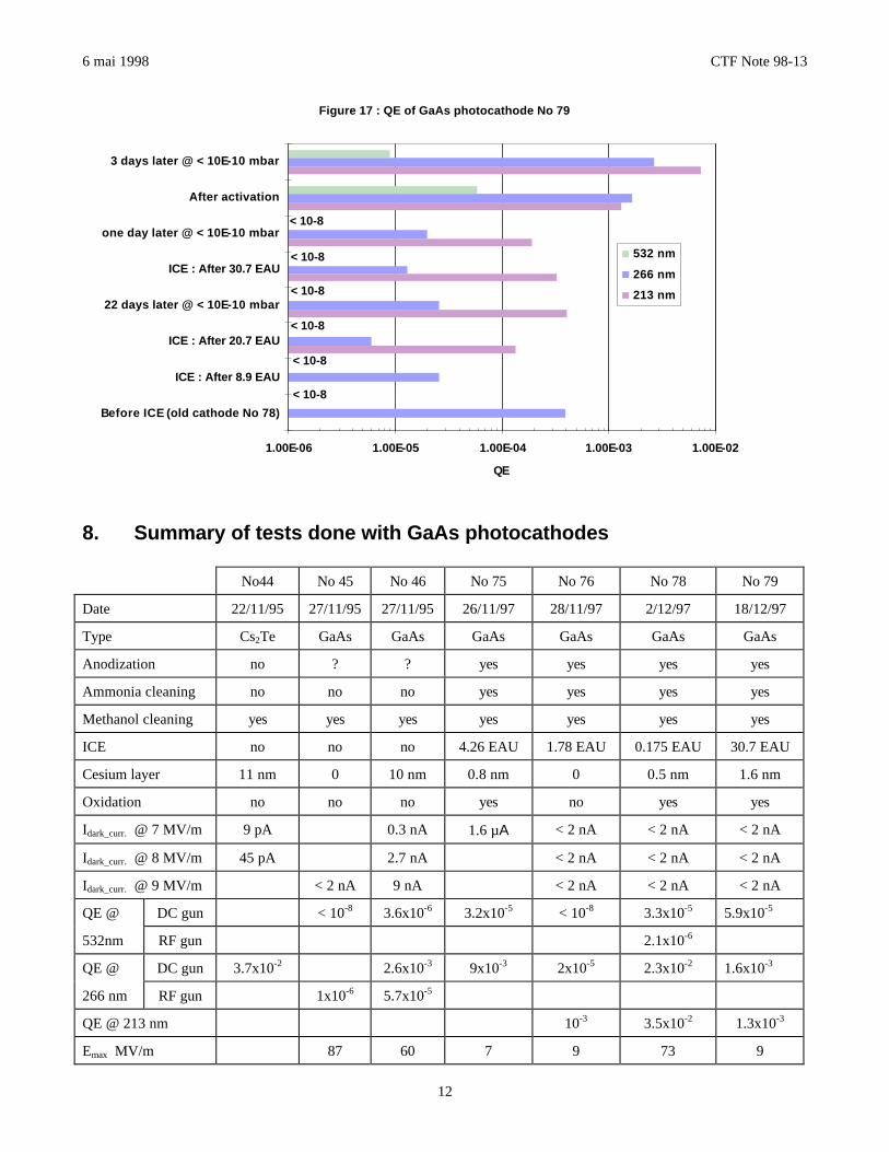
Table 3 and figure 17 summarize the main characteristics of this photocathode.
Table 3 : cathode 79
QE at λ = 213 nm QE at λ = 266 nm QE at λ = 532 nmBefore ICE (cath. 78) 4x10⁻⁴ < 10-8
ICE : 8.9 EAU 2.6x10⁻⁵ < 10-8
ICE :20.7 EAU 1.3x10⁻⁴ 6x10⁻⁶ < 10-8
22 days later a) 4.1x10⁻⁴ 2.6x10⁻⁵ < 10-8
ICE : 30.7 EAU 3.3x10⁻⁴ 1.3x10⁻⁵ < 10-8
one day later a) 1.9x10⁻⁴ 2x10⁻⁵ < 10-8
After activation b) 1.33x10⁻³ 1.65x10⁻³ 5.9x10⁻⁵
3 days later a) 7.3x10⁻³ 2.7x10⁻³ 9x10⁻⁶
a) The cathode is stored inside a vacuum pressure better than 10-10 mbarb) Deposition of 1.64 nm of cesium under about 10-9 mbar of oxygen pressure
6 mai 1998 CTF Note 98-13
12
Figure 17 : QE of GaAs photocathode No 79
1.00E-06 1.00E-05 1.00E-04 1.00E-03 1.00E-02
Before ICE (old cathode No 78)
ICE : After 8.9 EAU
ICE : After 20.7 EAU
22 days later @ < 10E-10 mbar
ICE : After 30.7 EAU
one day later @ < 10E-10 mbar
After activation
3 days later @ < 10E-10 mbar
QE
532 nm
266 nm
213 nm
< 10-8
< 10-8
< 10-8
< 10-8
< 10-8
< 10-8
8. Summary of tests done with GaAs photocathodes
No44 No 45 No 46 No 75 No 76 No 78 No 79
Date 22/11/95 27/11/95 27/11/95 26/11/97 28/11/97 2/12/97 18/12/97
Type Cs2Te GaAs GaAs GaAs GaAs GaAs GaAs
Anodization no ? ? yes yes yes yes
Ammonia cleaning no no no yes yes yes yes
Methanol cleaning yes yes yes yes yes yes yes
ICE no no no 4.26 EAU 1.78 EAU 0.175 EAU 30.7 EAU
Cesium layer 11 nm 0 10 nm 0.8 nm 0 0.5 nm 1.6 nm
Oxidation no no no yes no yes yes
Idark_curr. @ 7 MV/m 9 pA 0.3 nA 1.6 µA < 2 nA < 2 nA < 2 nA
Idark_curr. @ 8 MV/m 45 pA 2.7 nA < 2 nA < 2 nA < 2 nA
Idark_curr. @ 9 MV/m < 2 nA 9 nA < 2 nA < 2 nA < 2 nA
QE @ DC gun < 10-8 3.6x10⁻⁶ 3.2x10⁻⁵ < 10-8 3.3x10⁻⁵ 5.9x10⁻⁵
532nm RF gun 2.1x10⁻⁶
QE @ DC gun 3.7x10⁻² 2.6x10⁻³ 9x10⁻³ 2x10⁻⁵ 2.3x10⁻² 1.6x10⁻³
266 nm RF gun 1x10⁻⁶ 5.7x10⁻⁵
QE @ 213 nm 10-3 3.5x10⁻² 1.3x10⁻³
Emax MV/m 87 60 7 9 73 9

6 mai 1998 CTF Note 98-13
13
Ion bombardment cleaning and activation on GaAs photocathodes
QE on photocathode No 75
1.E-06 1.E-05 1.E-04 1.E-03 1.E-02 1.E-01
Before ICE
ICE : After 4.26 EAU
After activation
QE
532 nm
266 nm
213 nm
< 10-8
< 10-8
1 EAU = 1 joule Argon plasma energy at 75x10-3 mbar
QE on photocathode No 76
1.00E-06 1.00E-05 1.00E-04 1.00E-03 1.00E-02 1.00E-01
Before ICE
ICE : After 1.78EAU
QE
532 nm
266 nm
213 nm
< 10-8
< 10-8
QE on photocathode No 78
1.E-06 1.E-05 1.E-04 1.E-03 1.E-02 1.E-01
Before ICE
ICE : After 0.05 EAU
ICE : After 0.1 EAU
ICE : After 0.175EAU
6 days later @ <10E-10 mbar
After activation
CTF meas. (1 daylater)
9 days afteractivation
QE
532 nm
266 nm
213 nm
< 10-8
< 10-8
< 10-8
< 10-8
< 10-8
< 10-8
QE on photocathode No 79
1.00E-06 1.00E-05 1.00E-04 1.00E-03 1.00E-02
Before ICE (oldcathode No 78)
ICE : After 8.9EAU
ICE : After 20.7EAU
22 days later @ <10E-10 mbar
ICE : After 30.7EAU
one day later @ <10E-10 mbar
After activation
3 days later @ <10E-10 mbar
QE
532 nm
266 nm
213 nm
< 10-8
< 10-8
< 10-8
< 10-8
< 10-8
< 10-8

6 mai 1998 CTF Note 98-13
14
9. ConclusionGaAs requires different techniques compared to the Cs2Te preparation with which we are familiar. We were not able withthe available equipment to overcome the lack of:
• heating up to 600 °C with temperature control for UHV bake out.• monitoring online using red or infra red light during cesium evaporation and oxidation.• transferring the GaAs photocathode within a short time ( < half an hour) from the photo-emission lab to the
CTF RF gun.However, the injection of low pressure oxygen inside the preparation chamber was finally achieved.Electronic microscope observation of the test samples reveals no damage on the surface of the GaAs material, damageattributable to the ICE cleaning process or the 7 MV/m electric field in the DC gun.