Gallium arsenide based Buried Heterostructure Laser Diodes ...9091/FULLTEXT01.pdf · Gallium...
109
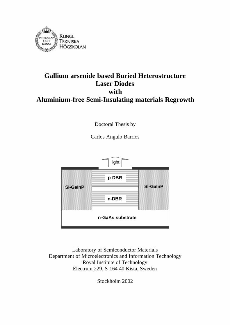
Gallium arsenide based Buried Heterostructure Laser Diodes with Aluminium-free Semi-Insulating materials Regrowth Doctoral Thesis by Carlos Angulo Barrios Laboratory of Semiconductor Materials Department of Microelectronics and Information Technology Royal Institute of Technology Electrum 229, S-164 40 Kista, Sweden Stockholm 2002 SI-GaInP n-GaAs substrate p-DBR n-DBR light SI-GaInP
Transcript of Gallium arsenide based Buried Heterostructure Laser Diodes ...9091/FULLTEXT01.pdf · Gallium...
Gallium arsenide based Buried HeterostructureLaser Diodes
withAluminium-free Semi-Insulating materials Regrowth
Doctoral Thesis by
Carlos Angulo Barrios
Laboratory of Semiconductor MaterialsDepartment of Microelectronics and Information Technology
Royal Institute of TechnologyElectrum 229, S-164 40 Kista, Sweden
Stockholm 2002
SI-GaInP
n-GaAs substrate
p-DBR
n-DBR
light
SI-GaInP

Cover picture: Schematic cross-section of a buried heterostructure VCSELincorporating semi-insulating GaInP:Fe as the burying layer. The work on this laserwas pointed out as one of the highlights in this field by the magazine CompoundSemiconductor, 6(7) Sept./Oct. 2000.

To my parents for their never-ending support


One shouldn’t work on semiconductors, that is a filthy mess;
who knows whether they really exist.
Wolfgang Pauli, 1931
Well, in that case, one should consider semi-insulating materials as a filthy mess full of traps, which is even worse;
sometimes they exist, sometimes they don’t.
The author

i
Carlos Angulo BarriosGallium arsenide based buried heterostructure semiconductor lasers with aluminium-free semi-insulating materials regrowth.
Department of Microelectronics and Information Technology, Laboratory ofSemiconductor Materials, Royal Institute of Technology, S-164 40 Kista, Sweden
ISRN KTH/HMA/FR-02/1-SE/TRITA-HMA Report 2002:1/ISSN 1404-0379
Abstract
Semiconductor lasers based on gallium arsenide and related materials arewidely used in applications such as optical communication systems, sensing, compactdisc players, distance measurement, etc. The performance of these lasers can beimproved using a buried heterostructure offering lateral carrier and opticalconfinement. In particular, if the confinement (burying) layer is implemented byepitaxial regrowth of an appropriate aluminium-free semi-insulating (SI) material,passivation of etched surfaces, reduced tendency to oxidation, low capacitance andintegration feasibility are additional advantages.
The major impediment in the fabrication of GaAs/AlGaAs buried-heterostructure lasers is the spontaneous oxidation of aluminium on the etched wallsof the structure. Al-oxide acts as a mask and makes the regrowth process extremelychallenging. In this work, a HCl gas-based in-situ cleaning technique is employedsuccessfully to remove Al-oxide prior to regrowth of SI-GaInP:Fe and SI-GaAs:Fearound Al-containing laser mesas by Hydride Vapour Phase Epitaxy. Excellentregrowth interfaces, without voids, are obtained, even around AlAs layers.Consequences of using inadequate cleaning treatments are also presented. Regrowthmorphology aspects are discussed in terms of different growth mechanisms.
Time-resolved photoluminescence characterisation indicates a uniform Fe trapdistribution throughout the regrown GaInP:Fe. Scanning capacitance microscopymeasurements demonstrate the semi-insulating nature of the regrown GaInP:Fe layer.The presence of EL2 defects in regrown GaAs:Fe makes more difficult theinterpretation of the characterisation results in the near vicinity of the laser mesa.
GaAs/AlGaAs buried-heterostructure lasers, both in-plane lasers and vertical-cavity surface-emitting lasers, with GaInP:Fe as burying layer are demonstrated forthe first time. The lasers exhibit good performance demonstrating that SI-GaInP:Fe isan appropriate material to be used for this purpose and the suitability of our cleaningand regrowth method for the fabrication of this type of semiconductor lasers. Devicecharacterisation indicates negligible leakage current along the etched mesa sidewallsconfirming a smooth regrowth interface. Nevertheless, experimental and simulationresults reveal that a significant part of the injected current is lost as leakage throughthe burying material. This is attributed to double carrier injection into the SI-GaInP:Fe layer. Simulations also predict that the function of GaInP:Fe as currentblocking layer should be markedly improved in the case of GaAs-based longerwavelength lasers.
Index Terms: semiconductor lasers, in-plane lasers, VCSELs, GaAs, GaInP, semi-insulating materials, hydride vapour phase epitaxy, regrowth, buried heterostructure,leakage current, simulation.

ii
iii
Preface
This thesis is a result of the research on the applications of Al-free semi-insulatingmaterials for fabricating GaAs-based buried-heterostructure semiconductor lasers. Asa consequence, it deals with the fabrication, performance and analysis of these lasers.Different facets related to the subject of the thesis are: epitaxial growth and cleaningtechniques of III-V semiconductor materials, device process technology, materialscharacterisation, device characterisation and theoretical analysis by computersimulation.
The thesis is divided into three parts. Part I presents an introduction to the subject, thestate-of-the-art, motivation and aims of the work. Part II reviews some of the basicsnecessary to follow more easily the original work. Part III contains the developmentof the original work, summary, conclusions and proposals for future research. Anappendix illustrates the processing steps of buried heterostructure laser diodefabrication. Reprints of the papers are attached at the end.

iv
v
Acknowledgements
The realisation of this thesis was possible thanks to the work and efforts ofmany people and now it is time to thank all of them. First, I would like to thank Prof.Gunnar Landgren, head of the Laboratory of Semiconductor Materials (HMA), foraccepting me as a Ph.D. student at KTH.
The major part of this thesis work was supported by NUTEK, within theframework of ERGO/KOFUMA programme. Actually, this thesis could beconsidered as the final report of that project. The main characters of thiscollaboration have been:
Dr. Sebastian Lourdudoss, called “Doss” by his friends, that is, everybody.Scientist, teacher, poet, family man, and one of the most generous persons I have evermet. He has been my supervisor and friend during these years as a Ph.D. student. Hisinexhaustible and contagious optimism and enthusiasm gave me the necessary energyduring the “hard times”, when the materials we were studying seemed to be “semi-insulting” rather than semi-insulating. “Things work according to one’s own belief”,he told me once. Since then, I become a “believer”. Despite his numerous andgrowing occupations, he had ALWAYS time for my infinite and disturbing questions.I will be never able to express enough my gratitude to him.
Dr. Egbert Rodríguez Messmer, my first contact and friend in Sweden. Hewas my teacher in the lab and revealed me the secrets of the (g)old HVPE reactor.His help and expertise were determinant in the development of this work. It has beena pleasure to work with him. Outside the lab, he also taught me Swedish habits, rules,bureaucracy and other issues that made my incorporation into the “machinery” easier,and introduced to me many interesting and nice people. Since I knew that he was aReal Madrid supporter, I realised that we were going to speak the same language. Healso induced me indirectly to run Stockholm Marathon twice and Stockholms Loppet…although I am not sure if I should be grateful for that....
Martin Holmgren from the former Spectra Precision (now Trimble). Heprovided IPL structures and mounting and characterisation facilities at SPA. AnitaLövqvist and Dr. Marco Ghisoni from the former Mitel Semiconductors (nowZarlink). Anita provided VCSEL structures and worked very hard on the processingof BH-VCSELs. Christina Carlsson, John Halonen and Prof. Anders Larsson fromChalmers University of Technology. Christina made VCSEL characterisation andJohn worked on the dry etching of the VCSELs. Andreas Gaarder (excellent pianistand master of wines) and Dr. Saulius Marcinkevicious (expert in Viking stories andLithuanian basketball) from the Optics department at KTH worked on the TR-PLcharacterisation. A smooth collaboration with all these people has been extremelybeneficial. I am extremely lucky for having worked with such extraordinary group ofprofessionals from industry and academia, and I thank all of them for their help andcontribution to this work.
In addition, other remarkable people not “officially” included in the projecthave also contributed significantly to this thesis. Christiane Buchgeister and LenaBäckbom helped me in the clean room during laser processing. I learnt manyprocessing skills from them. Olivier Douhéret (Ph.D. in enthusiasm) and Dr.Srinivasan Anand worked on the SCM measurements. I enjoyed very muchdiscussing scientific and non-scientific topics with Anand. Dr. Renaud Stevensmeasured high-speed performance of the VCSELs. Dr. Richard Schatz helped me tounderstand the high frequency modulation results of BH-VCSELs. Dr. Hans
vi
Martinsson from Chalmers did electroluminescence measurements on the IPLs. I hadalso very fruitful discussions with Sebastian Mogg and Dr. Olle Kjebon onsemiconductor laser physics.
I must dedicate a special section to the HVPE group. Dr. David Söderström, aSwede with Latin soul; his passion for dancing salsa is only comparable to hismeticulous work procedures. I learnt many things from him. Dr. Denis Jahan, myfirst officemate; we had interesting discussions about French and Spanish issues,although we never agreed. Fortunately, we had a common passion, both of us love“heavy music”, and Denis plays “Metallica” songs “almost” as well as JamesHetfield. Dr. Jérôme Napierala, with whom I had always interesting discussions oncrystal growth. And, finally, Yanting Sun, who disclosed the Chinese culture to me.
I thank Gunnar Andersson for the assistance in the HVPE reactormaintenance.
I am very grateful to the rest of the members and ex-members of HMA for afriendly and helpful atmosphere: Carl Asplund, Dr. Krishnan Baskar, AndreasBentzen, Jesper Berggren, Roberta Campi, Carl-Fredrik Carlström, Nicolae Chitica,Peter Goldmann, Dr. Mattias Hammar, Dr. Dietmar Keiper, Cyril Menon, MikaelMulot, Fredrik Olsson, Amit Patel, Glenn Plaine, Dr. Henry Radamsson, Dr. FredrikSalomonsson, Martin Strassner and Petrus Sundberg.
Agneta Odéen, Margreth Hellberg and Rose-Marie Lövenstig helped menicely and efficiently with all the administrative issues.
Sang-Kwon Lee helped me with the probe station measurements. I thank JulioMercado and Richard Andersson for computer system assistance.
I also thank Dr. María Alonso from the Instituto de Ciencia de los Materialesde Madrid for her collaboration and spending hours working on AES measurements.
I would like to thank Dr. José Luis García Tijero, Prof. Elías Muñoz, and Prof.Tomás Rodríguez from the Universidad Politécnica de Madrid for their support andwise advice.
I wish to thank Doss’ family: Alphonsa (she cooks chicken as the angels),Cecilia, Pierre and Ilango, for very nice lunches and… interesting chess games (myreal passion).
Many thanks to the great people I have met in Sweden for very good times:Manuel and Kristina, Juan Peña, Alvaro, Nacho, Diego, Jose, Delia, Patricia, Raquel,Minna, Ana, Hector, “torpedo” Jenia, Henrik, Juan Caballero, Oscar…
And, of course, I cannot forget those who have supported me from far away. Ideeply thank all my friends from Spain for keeping frequent contacts and remindingme the pleasures of Spanish life every time I went “down there” back. Eduardo,Angel, Alicia, Enrique, Jesús, Paco, César, the immortal “Area VI”, i.e., Yolanda,Raúl, Lucas, Nacho, Rafa and Enrique (“el melenas”); José Luis, Fernando, Ana…Iwould like to mention all the names, but this report is already thick enough, sorry.
Finally, very special thanks to my family, mainly to my parents, for theirinfinite support, patience and understanding.
Thank you all.Stockholm,
January 25, 2002
Audentis Fortuna iuvat [Fortune assists the bold]
vii
List of papers
Paper AC. Angulo Barrios, E. Rodríguez Messmer, M. Holmgren, A. Risberg, J. Halonen, andS. Lourdudoss, ”Epitaxially regrown GaAs/AlGaAs laser mesas with semi-insulatingGaInP:Fe and GaAs:Fe,” Journal of Electronic Materials, Vol. 30, No. 8, pp. 987-991, 2001.
Contributions by the author of this thesis: Major part of the experiments, analysis, andwriting.
Paper BA. Gaarder, S. Marcinkevicius, C. Angulo Barrios, and S. Lourdudoss, “Time-resolved micro-photoluminescence studies of deep level distribution in selectivelyregrown GaInP:Fe and GaAs:Fe,” Semiconductor Science and Technology, 17, pp.129-134, 2002.
Contributions by the author of this thesis: Regrowth experiments, and part of theinterpretation, discussion and writing.
Paper CA. Gaarder, S. Marcinkevicius, C. Angulo Barrios, and S. Lourdudoss, “Time-resolved micro-photoluminescence studies of dopant distribution in selectivelyregrown GaInP:Fe around VCSELs,” accepted for publication in Physica Scripta.
Contributions by the author of this thesis: Regrowth experiments, and part of theinterpretation, discussion and writing.
Paper DO. Douhéret, S. Anand, C. Angulo Barrios, and S. Lourdudoss, “Characterisation ofGaAs/AlGaAs buried-heterostructure lasers by scanning capacitance microscopy,”12th International Conference on Microscopy of Semiconducting Materials, Oxford,UK, 2001, paper P3-23.
Contributions by the author of this thesis: Regrowth experiments, and part of theinterpretation and discussion.
Paper EC. Angulo Barrios, E. Rodríguez Messmer, M. Holmgren, and S. Lourdudoss,“GaAs/AlGaAs buried heterostructure laser by wet etching and semi-insulatingGaInP:Fe regrowth,” Electrochemical and Solid State Letters, 3 (9), pp. 439-441,2000.
Contributions by the author of this thesis: Laser fabrication, major part ofcharacterisation, and writing.
viii
Paper FC. Angulo Barrios, E. Rodríguez Messmer, A. Risberg, C. Carlsson, J. Halonen, M.Ghisoni, A. Larsson, and S. Lourdudoss, “GaAs/AlGaAs buried-heterostructurevertical-cavity surface-emitting laser with semi-insulating GaInP:Fe regrowth,”Electronics Letters, Vol. 36, No. 18, pp. 1542-1544, 2000.
Contributions by the author of this thesis: Part of laser fabrication, lasercharacterisation, and writing.
Paper GC. Carlsson, C. Angulo Barrios, E. Rodríguez Messmer, A. Lövqvist, J. Halonen, J.Vukusic, M. Ghisoni, S. Lourdudoss, and A. Larsson, “Performance characteristics ofburied heterostructure VCSELs using semi-insulating GaInP:Fe regrowth,” IEEEJournal of Quantum Electronics, Vol. 37, No. 7, pp. 945-950, 2001.
Contributions by the author of this thesis: Part of laser fabrication and discussion.
Paper HR. Stevens, R. Schatz, A. Lövqvist, T. Aggerstam, C. Carlsson, C. Angulo Barrios, S.Lourdudoss, and M. Ghisoni, “Quest for very high-speed VCSELs: pitfalls andclues,” Optoelectronics 2001 – Integrated Optoelectronics Devices, paper 4286-11,San Jose, USA, January 2001 (invited paper).
Contributions by the author of this thesis: Part of BH-laser fabrication,characterisation and discussion.
Paper IC. Angulo Barrios, S. Lourdudoss, and H. Martinsson, “Analysis of leakage current inGaAs/AlGaAs BH lasers with semi-insulating GaInP:Fe burying layer,” Submitted forpublication.
Contributions by the author of this thesis: Design, simulation, theoretical andexperimental analyses, and writing.
ix
Additional papers not included in this thesis
1. A. Gaarder, C. Angulo Barrios, E. Rodríguez Messmer, S. Lourdudoss, and S.Marcinkevicius, “Dopant distribution in selectively regrown InP:Fe and InGaP:Festudied by time-resolved photoluminescence,” 12th International Conference onInP and Related Materials (IPRM), Williamsburg, USA, 2000 (paper WB3.2).Conference Proceedings (IEEE, Piscataway, 2000), p. 518-521.
2. A. Gaarder, S. Marcinkevicius, C. Angulo Barrios, E. Rodríguez Messmer, and S.Lourdudoss, “Time resolved microphotoluminescence of selectively regrownInP:Fe and InGaP:Fe structures,” Northern Optics 2000, paper OR1, Uppsala,Sweden, June 2000.
3. C. Angulo Barrios, E. Rodríguez Messmer, M. Holmgren, and S. Lourdudoss,“Semi-insulating GaInP:Fe and GaAs:Fe regrowth around GaAs/AlGaAs lasermesas,” 3rd International Conference on Materials for Microelectronics, Dublin,Ireland, 2000, p. 157.
4. S. Lourdudoss, D. Söderström, C. Angulo Barrios, Y. Sun, and E. RodríguezMessmer, “Semi-insulating epitaxial layers for optoelectronic devices,” 2000International Semiconducting and Insulating Materials Conference, Canberra,Australia, 2000. SIMC-XI, Editors C. Jagadish and N.J. Welham, IEEEPublishing, 2001, ISBN 0-7803-5815-5, p.171 (invited paper).
5. A. Gaarder, S. Marcinkevicius, C. Angulo Barrios, and S. Lourdudoss, “Time-resolved photoluminescence studies of dopant distribution in selectively regrownGaInP:Fe around VCSELs,” 19th Nordic Semiconductor Conference, Copenhagen,Denmark, 2001.
6. C. Angulo Barrios, S. Lourdudoss, E. Rodríguez Messmer, M. Holmgren, A.Lövqvist, C. Carlsson, A. Larsson, J. Halonen, M. Ghisoni, R. Stevens, and R.Schatz, “GaAs/AlGaAs buried-heterostructure laser diodes with semi-insulatingGaInP:Fe regrowth,” 4th Pacific Rim Conference on Lasers and Electro-Optics(CLEO/PR), Chiba, Japan, 2001, paper ThC1-4, p. II.590.
7. O. Douhéret, S. Anand, C. Angulo Barrios, and S. Lourdudoss, “Characterisationof GaAs/AlGaAs laser mesas regrown with semi-insulating GaInP by scanningcapacitance microscopy,” Submitted for publication.

x

xi
Acronyms
ALE Atomic-Layer EpitaxyAFM Atomic Force MicroscopyBH Buried HeterostructureCARIBE Chemically Assisted Reactive Ion Beam EtchingCBE Chemical Beam EpitaxyCl-VPE Chloride Vapour Phase EpitaxyCW Continuous WaveDBR Distributed Bragg ReflectorDFB Distributed Feed BackDLTS Deep Level Transient SpectroscopyFWHM Full Width at Half MaximumHRXRD High Resolution X-Ray DiffractionHVPE Hydride Vapour Phase EpitaxyIPL In-Plane LaserI-V Current-VoltageI-V-T Current-Voltage-TemperatureLASER Light Amplification of Stimulated Emission RadiationLED Light Emitting DiodeLD Laser DiodeL-I Light-CurrentLTG Low Temperature GrowthLPE Liquid Phase EpitaxyMBE Molecular Beam EpitaxyMCEF Modulation Current Efficiency FactorMIS Metal-Insulator-SemiconductorMOCVD Metal Organic Chemical Vapour DepositionMOMBE Metal Organic Molecular Beam EpitaxyMOVPE Metal Organic Vapour Phase EpitaxyMQW Multiple Quantum WellOEIC OptoElectronic Integrated CircuitPBH Planar Buried HeterostructurePECVD Plasma Enhanced Chemical Vapour Depositionppm Parts Per MillionRT Room Temperaturesccm Standard Cubic Centimetre per MinuteSCM Scanning Capacitance MicroscopySCH Separate Confinement HeterostructureSEM Scanning Electron MicroscopySI Semi-InsulatingSIMS Secondary Ion Mass SpectroscopySQW Single Quantum WellSRH Shockley-Read-HallTR-PL Time-Resolved Photo-LuminescenceVCSEL Vertical-Cavity Surface-Emitting Laser2-D Two-dimensional

xii
xiii
ContentsAbstract iPreface iiiAcknowledgements vList of papers viiAcronyms xi
I. Introduction 1
II. Background 5II.1. III-V semiconductor materials 5II.2. Zincblende lattice 7II.3. Epitaxy of III-V materials 9
II.3.1. Epitaxial techniques 9II.3.2. Hydride Vapour Phase Epitaxy (HVPE) 11
II.4. Semi-insulating III-V materials 13II.4.1. Deep levels 13II.4.2. Fully compensated III-V semiconductors 16II.4.3. Carrier injection in SI materials 17II.4.4. Semi-insulating Ga0.51In0.49P:Fe and GaAs:Fe 18
II.5. Techniques for characterising regrown SI materials 20 II.5.1. Time-resolved photoluminescence (TR-PL) 21
II.5.2. Scanning capacitance microscopy (SCM) 22II.6. Semiconductor laser characterisation 23
II.6.1. Static characteristics 23II.6.2. Dynamic characteristics 26
II.7. Leakage current in buried heterostructure laser diodes 28
III. Original work 31 III.1. Epitaxial regrowth around Al-containing laser mesas 31
III.1.1. GaInP and GaAs properties 31 III.1.2. Al-oxide cleaning procedures 34 III.1.3. HCl-based in-situ cleaning 37
III.1.4. Regrowth morphology 40III.2. Regrowth characterisation 44
III.2.1. Time-resolved photoluminescence characterisation 44 III.2.2. Scanning capacitance microscopy characterisation 49
III.3. Buried heterostructure laser diodes 51III.3.1. BH In-Plane Lasers 51III.3.2. BH VCSELs 59
III.4. Analysis of leakage current 68III.5. Summary, conclusions and future work 74
Appendix: BH laser processing 77References 81Reprints of papers 90

xiv
1
I. INTRODUCTION
Optoelectronics is one of the pillars of the so-called information technologies andplays an important role in our modern life. Discrete and integrated optoelectronicdevices are used in numerous applications1: consumer electronics (compact disc (CD)players, laser printers, cameras,…), telecommunications (internet, cable tv, loopfeeders, bypass private networks, undersea,…), data communications (local areanetworks, equipment interconnects, machine control,…), defence and aviation (radar,airborne systems, electronic warfare, surveillance,…). This has made optoelectronicsimportant in the world economy and one of the fastest emerging fields in the differentindustrial sectors2.
Semiconductor lasers are perhaps, on account of the economic standards and thedegree of theirs applications, the most important of all lasers. Every CD player andCD-ROM has one such laser, and so does every hand-held barcode scanner. It isnearly impossible to make a long-distance call without them, and high-speed datalinks depend on them, too. The main features that have made the semiconductorlasers the most popular light sources for such applications are: small physical size (afew hundred µm in size), electrical pumping, high efficiency in converting electricpower to light, direct modulation (this is of major importance in high-data-rate opticalcommunication systems), possibility of integrating it monolithically with electronicand optical components to form OEICs (optoelectronic integrated circuits), opticalfiber compatibility, and mass production using the mature semiconductor-basedmanufacturing technology.
A semiconductor laser is basically a p-n diode structure placed inside an opticalcavity. Under forward bias, charge carriers are injected into a thin active layerproviding an optical gain. The optical cavity can be achieved in different ways. Asimple Fabry-Perot resonator is obtained by parallel cleaved facets [Fabry-Perot (FP)lasers]. Light feedback can also be provided in a distributed manner by a series ofclosely spaced reflectors as in distributed-feedback (DFB) lasers, distributed Braggreflector (DBR) lasers and vertical cavity surface emitting lasers (VCSELs)3. FP,DFB and DBR lasers are called edge emitting or in-plane lasers (IPLs) because theactive layer plane is parallel to the direction of the laser beam, which is emitted at theedges of the laser chip. On the other hand, vertical cavity surface emitting lasers havethe plane of the active layer perpendicular to the direction of the laser beam, which isemitted at the top or bottom surface of the chip.
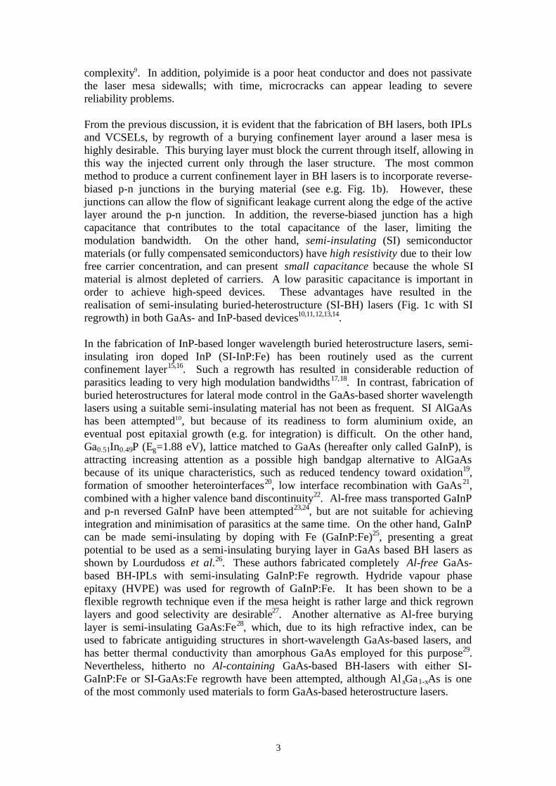
The practical semiconductor laser is designed to laterally confine current, carriers, andphotons within the laser structure in order to achieve high efficiency devices andsingle-lateral-mode operation, which is an imperative issue in applications such asoptical fiber-based communication, optical interconnection and optical informationprocessing4. In IPLs, this is achieved in stripe laser geometries in which a narrowstrip of active region defines the laser axis. Several stripe laser designs are illustratedin Fig. 1. The oxide stripe laser structure has some lateral current confinement, but nolateral carrier or photon confinement, making its commercial value limited; in thisstructure the optical modes are confined by the lateral variation of the optical gain,and therefore, it is called gain-guided laser. Implanted stripe lasers use ionimplantation to form semi-insulating regions on either side of the stripe, in this waythe implanted region funnels the injection current into the active region (current
2
confinement), although this process does not result in significant carrier and opticalconfinement. On the other hand, buried heterostructure (BH) lasers (Fig. 1b and 1cwith semi-insulating regrowth) can provide good current, carrier and opticalconfinement simultaneously5. In BH lasers the active region is completely buriedinside a higher-bandgap lower-index semiconductor material, producing an opticalwaveguide geometry (index-guided lasers) that has both excellent carrier and opticalconfinement. It must be indicated that the burying layer can be also a lower-bandgaphigher-index material making use of the antiguiding effect to obtain stable single-lateral mode lasers3, although the allowance of optical loss for high-order lateralmodes makes the lasing quantum efficiency low. In addition to these confinementproperties, a good thermal conductivity of the burying layer can improve thedissipation of heat that is generated during the lasing action. Besides, the buryingprocess consisting in regrowing a material lattice matched to the laser structurearound the etched laser mesas may passivate the defects on the mesa sidewalls(surface passivation) created during the etching process. This leads to a reduction ofthe leakage current (current component which does not pass through the activeregion)6, and can provide planar structures, which facilitate further processing.
Figure 1. Schematic cross section of different stripe laser geometries showing an (a)oxide, (b) p-n reversed and (c) semi-insulating (implanted or regrowth) stripestructures. Configurations (b) and (c) with SI regrowth are BH laser diodes.
In VCSELs, besides ion-implanted7 and buried heterostructure8 configurations (withthe same fundamental features as those mentioned for IPLs), small oxide-apertures arealso used for both current and optical confinement9. Although such oxide aperturescan be produced with high yield and uniformity, this configuration results in largecapacitance associated to the thin oxidised layer and a non-planar topology. This hasled to use thick layers of polyimide around etched VCSEL mesas under the bond padto reduce the capacitance and achieve planarisation, which increases the fabrication
n+ substrate
n+ substrate
n+ substrate
n-cladding
p-cladding
metal
metal
oxide
active
n n
p p
p
n
metal
metal
metal
metal
p
n
SI SI
(a) (b)
(c)
3
complexity9. In addition, polyimide is a poor heat conductor and does not passivatethe laser mesa sidewalls; with time, microcracks can appear leading to severereliability problems.
From the previous discussion, it is evident that the fabrication of BH lasers, both IPLsand VCSELs, by regrowth of a burying confinement layer around a laser mesa ishighly desirable. This burying layer must block the current through itself, allowing inthis way the injected current only through the laser structure. The most commonmethod to produce a current confinement layer in BH lasers is to incorporate reverse-biased p-n junctions in the burying material (see e.g. Fig. 1b). However, thesejunctions can allow the flow of significant leakage current along the edge of the activelayer around the p-n junction. In addition, the reverse-biased junction has a highcapacitance that contributes to the total capacitance of the laser, limiting themodulation bandwidth. On the other hand, semi-insulating (SI) semiconductormaterials (or fully compensated semiconductors) have high resistivity due to their lowfree carrier concentration, and can present small capacitance because the whole SImaterial is almost depleted of carriers. A low parasitic capacitance is important inorder to achieve high-speed devices. These advantages have resulted in therealisation of semi-insulating buried-heterostructure (SI-BH) lasers (Fig. 1c with SIregrowth) in both GaAs- and InP-based devices10,11,12,13,14.
In the fabrication of InP-based longer wavelength buried heterostructure lasers, semi-insulating iron doped InP (SI-InP:Fe) has been routinely used as the currentconfinement layer15,16. Such a regrowth has resulted in considerable reduction ofparasitics leading to very high modulation bandwidths17,18. In contrast, fabrication ofburied heterostructures for lateral mode control in the GaAs-based shorter wavelengthlasers using a suitable semi-insulating material has not been as frequent. SI AlGaAshas been attempted10, but because of its readiness to form aluminium oxide, aneventual post epitaxial growth (e.g. for integration) is difficult. On the other hand,Ga0.51In0.49P (Eg=1.88 eV), lattice matched to GaAs (hereafter only called GaInP), isattracting increasing attention as a possible high bandgap alternative to AlGaAsbecause of its unique characteristics, such as reduced tendency toward oxidation19,formation of smoother heterointerfaces20, low interface recombination with GaAs21,combined with a higher valence band discontinuity22. Al-free mass transported GaInPand p-n reversed GaInP have been attempted23,24, but are not suitable for achievingintegration and minimisation of parasitics at the same time. On the other hand, GaInPcan be made semi-insulating by doping with Fe (GaInP:Fe)25, presenting a greatpotential to be used as a semi-insulating burying layer in GaAs based BH lasers asshown by Lourdudoss et al.26. These authors fabricated completely Al-free GaAs-based BH-IPLs with semi-insulating GaInP:Fe regrowth. Hydride vapour phaseepitaxy (HVPE) was used for regrowth of GaInP:Fe. It has been shown to be aflexible regrowth technique even if the mesa height is rather large and thick regrownlayers and good selectivity are desirable27. Another alternative as Al-free buryinglayer is semi-insulating GaAs:Fe28, which, due to its high refractive index, can beused to fabricate antiguiding structures in short-wavelength GaAs-based lasers, andhas better thermal conductivity than amorphous GaAs employed for this purpose29.Nevertheless, hitherto no Al-containing GaAs-based BH-lasers with either SI-GaInP:Fe or SI-GaAs:Fe regrowth have been attempted, although AlxGa1-xAs is oneof the most commonly used materials to form GaAs-based heterostructure lasers.
4
A major obstacle to epitaxial regrowth on AlGaAs material to form lateralheterointerfaces arises from the exposure of the Al-containing surfaces to theatmosphere after mesa etching. Aluminium is highly reactive and oxidises very fast.This oxide acts as a mask making a subsequent regrowth around the oxidised surfaceson the laser mesa sidewalls difficult. In addition, these oxides can degrade the laserperformance and shorten its lifetime. Furthermore, the oxides of high Al-containingAlGaAs layers are not self-terminating, and films, which are hundreds of nanometersthick, can be quickly consumed in the oxidation process. Aluminium oxides are morestable than Ga- and As-oxides (which, due to their volatility, are usually removed bythermal desorption) and it is very difficult, if not impossible, to remove them byconventional methods. Therefore, special procedures must be considered to eliminateAl-oxide before regrowth. Epitaxial regrowth on air exposed AlGaAs surfaces havebeen demonstrated by employing an in situ etch prior to regrowth by liquid phaseepitaxy (LPE) using a “melt-back” etch step30. In-situ etch has also been employedbefore metal-organic vapour phase epitaxy (MOVPE) regrowth through a thermal gasetch (usually HCl gas)31. However, the exposed AlGaAs layer can typically have anAlAs mole fraction of no greater than 10% and 50% for the LPE and MOVPE case,respectively30,31,32. Other means of achieving regrowth on AlGaAs surfaces is tosimply circumvent atmospheric exposure altogether by using protecting layers (e.g. aGaAs cap layer removable by a thermal HCl etch before regrowth by MOVPE33) orvacuum processing (maintaining vacuum conditions between etching and regrowth34).Oxide removal by hydrogen plasma prior to regrowth in MBE has beendemonstrated35. Nevertheless, no attempts to develop a method for the removal ofAlGaAs oxides prior to HVPE regrowth have been reported so far, although one ofthe strengths of HVPE resides in the epitaxial regrowth process27.
Based on the points discussed so far, it is easy to deduce the main motivation of thiswork: to extend the use of HVPE regrowth of semi-insulating GaInP:Fe to Al-containing structures for fabricating GaAs/AlGaAs-based BH lasers. It must also benoted that although most of the attention throughout this work has been focused onSI-GaInP:Fe, HVPE regrowth of SI-GaAs:Fe for the fabrication of similar BH lasershas also been investigated, motivated by the lack of composition-related issues andgood thermal properties of GaAs compared to GaInP.
Thus, the aims of this thesis are:
1) To achieve selective regrowth of Al-free semi-insulating III-V materials by HVPEaround Al-containing GaAs-based laser mesas.
2) To study the semi-insulating properties of the regrown material and interdiffusionof dopants between the regrown layer and the layers that constitute the laser.
3) To fabricate and characterise GaAs/AlGaAs BH lasers with GaInP:Fe (andGaAs:Fe) regrowth by HVPE.
4) To analyse theoretically GaAs based BH lasers with SI-GaInP:Fe burying layer tounderstand and predict the effect of material parameters and other deviceconfigurations on the laser performance.
Experimental procedures, results, analysis, discussion and conclusions about theachievement of each of these goals are described in Part III and the correspondingpapers at the end.
5
II. BACKGROUND
This section reviews important topics related to the subject of this thesis. The purposeis not to provide an extensive review of these issues, but to offer a brief description tofacilitate better understanding of the main content in part III.
Sections II.1 and II.2 outline the basic properties of III-V semiconductors, whilesection II.3 describes the most common techniques used for the epitaxial growth ofthese materials, with an emphasis on the hydride vapour phase epitaxy (HVPE)technique, which is of major importance in the development of this work. Section II.4explains how III-V semiconductors can be endowed with high resistivity, i.e., howthey can be made semi-insulating. Two particular cases of semi-insulating III-Vmaterials, GaInP:Fe and GaAs:Fe, have been the purpose of this work, and their mostsignificant properties are presented in this section. An adequate overview of twoexperimental techniques, time-resolved photoluminescence (TR-PL) and scanningcapacitance microscopy (SCM), used to characterise the aforementioned semi-insulating materials after regrowth by HVPE is given in section II.5. Section II.6presents the main concepts used to characterise the performance of semiconductorlasers under static and dynamic operation. Finally, in section II.7 the basicmechanisms that lead to leakage current in buried-heterostructure lasers arecommented.
II.1. III-V semiconductor materials
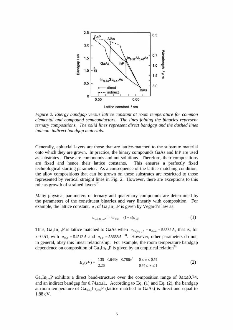
For optoelectronic applications, the device efficiency in emitting and detecting light isa major requirement. Elemental semiconductors such as Si, Ge and their alloys,Si1-xGex, are not appropriate materials for optoelectronic devices. Due to theirindirect fundamental bandgap, they emit light very poorly and their absorptioncoefficients are low36. On the other hand, several compound semiconductors and theiralloys offer many of the desired properties for optoelectronics purposes and can besynthesised without much difficulty. Compound semiconductors are made fromelements of different columns of the periodic table, for example, III-V and II-IVcompounds. Among all of them, III-V compound semiconductors are the most widelyused. In addition, ternary or quaternary semiconductor alloys made of three or fourgroup III and group V atoms can be realised. By modifying the atomic compositionof these alloys, it is possible to obtain different bandgaps and, therefore, varyingemission wavelengths for light sources. Fig. 2 illustrates the variation of the bandgap,Eg, (and the wavelength, λg [Eg(eV) = 1.24/λg(µm)]) as a function of lattice constantfor various compound and alloy semiconductors at room temperature.
The success of III-V materials for optoelectronic applications relies not only on thedirect bandstructure allowing for efficient light emission, but also on the ability tocreate heterostructures, that is, junctions of two semiconductors of unequal bandgaps.Heterojunctions are of paramount importance in the design of high-performanceelectronic and optoelectronic devices36.
6
Figure 2. Energy bandgap versus lattice constant at room temperature for commonelemental and compound semiconductors. The lines joining the binaries representternary compositions. The solid lines represent direct bandgap and the dashed linesindicate indirect bandgap materials.
Generally, epitaxial layers are those that are lattice-matched to the substrate materialonto which they are grown. In practice, the binary compounds GaAs and InP are usedas substrates. These are compounds and not solutions. Therefore, their compositionsare fixed and hence their lattice constants. This ensures a perfectly fixedtechnological starting parameter. As a consequence of the lattice-matching condition,the alloy compositions that can be grown on these substrates are restricted to thoserepresented by vertical straight lines in Fig. 2. However, there are exceptions to thisrule as growth of strained layers37.
Many physical parameters of ternary and quaternary compounds are determined bythe parameters of the constituent binaries and vary linearly with composition. Forexample, the lattice constant, a , of GaxIn1-xP is given by Vegard’s law as:
a xa x aGa In P GaP InPx x11
−= + −( ) (1)
Thus, GaxIn1-xP is lattice matched to GaAs when a a ÅGa In P GaAsx x156532
−= = . , that is, for
x=0.51, with a ÅGaP = 54512. and a ÅInP = 58688. 38. However, other parameters do not,in general, obey this linear relationship. For example, the room temperature bandgapdependence on composition of GaxIn1-xP is given by an empirical relation39:
E eVx x
g ( ). . ..
=+ +
135 0 643 0 7862 26
2
0 0 740 74 1
≤ ≤≤ ≤
xx
..
(2)
GaxIn1-xP exhibits a direct band-structure over the composition range of 0≤x≤0.74,and an indirect bandgap for 0.74≤x≤1. According to Eq. (1) and Eq. (2), the bandgapat room temperature of Ga0.51In0.49P (lattice matched to GaAs) is direct and equal to1.88 eV.
7
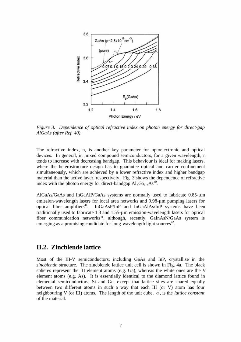
Figure 3. Dependence of optical refractive index on photon energy for direct-gapAlGaAs (after Ref. 40).
The refractive index, n, is another key parameter for optoelectronic and opticaldevices. In general, in mixed compound semiconductors, for a given wavelength, ntends to increase with decreasing bandgap. This behaviour is ideal for making lasers,where the heterostructure design has to guarantee optical and carrier confinementsimultaneously, which are achieved by a lower refractive index and higher bandgapmaterial than the active layer, respectively. Fig. 3 shows the dependence of refractiveindex with the photon energy for direct-bandgap AlxGa1-xAs40.
AlGaAs/GaAs and InGaAlP/GaAs systems are normally used to fabricate 0.85-µmemission-wavelength lasers for local area networks and 0.98-µm pumping lasers foroptical fiber amplifiers41. InGaAsP/InP and InGaAlAs/InP systems have beentraditionally used to fabricate 1.3 and 1.55-µm emission-wavelength lasers for opticalfiber communication networks41, although, recently, GaInAsN/GaAs system isemerging as a promising candidate for long-wavelength light sources42.
II.2. Zincblende lattice
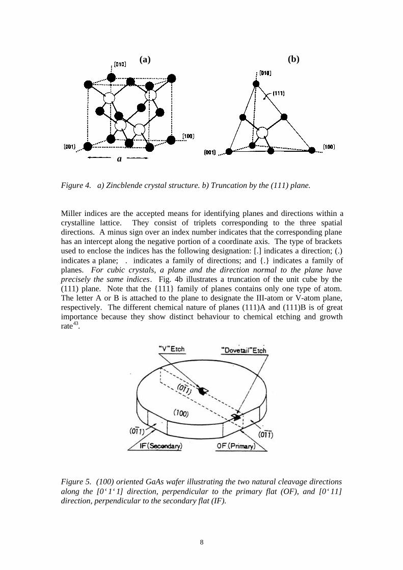
Most of the III-V semiconductors, including GaAs and InP, crystallise in thezincblende structure. The zincblende lattice unit cell is shown in Fig. 4a. The blackspheres represent the III element atoms (e.g. Ga), whereas the white ones are the Velement atoms (e.g. As). It is essentially identical to the diamond lattice found inelemental semiconductors, Si and Ge, except that lattice sites are shared equallybetween two different atoms in such a way that each III (or V) atom has fourneighbouring V (or III) atoms. The length of the unit cube, a , is the lattice constantof the material.
8
Figure 4. a) Zincblende crystal structure. b) Truncation by the (111) plane.
Miller indices are the accepted means for identifying planes and directions within acrystalline lattice. They consist of triplets corresponding to the three spatialdirections. A minus sign over an index number indicates that the corresponding planehas an intercept along the negative portion of a coordinate axis. The type of bracketsused to enclose the indices has the following designation: [.] indicates a direction; (.)indicates a plane; ⟨.⟩ indicates a family of directions; and . indicates a family ofplanes. For cubic crystals, a plane and the direction normal to the plane haveprecisely the same indices. Fig. 4b illustrates a truncation of the unit cube by the(111) plane. Note that the 111 family of planes contains only one type of atom.The letter A or B is attached to the plane to designate the III-atom or V-atom plane,respectively. The different chemical nature of planes (111)A and (111)B is of greatimportance because they show distinct behaviour to chemical etching and growthrate43.
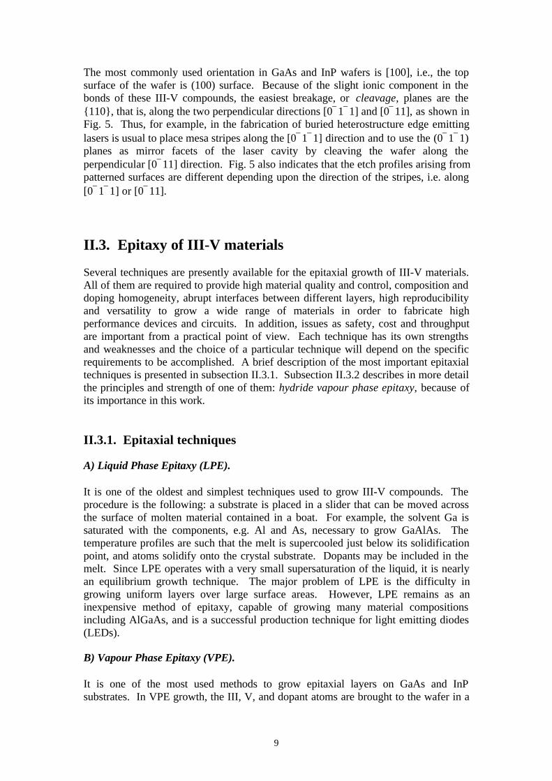
Figure 5. (100) oriented GaAs wafer illustrating the two natural cleavage directionsalong the [011] direction, perpendicular to the primary flat (OF), and [011]direction, perpendicular to the secondary flat (IF).
a
(a) (b)
9
The most commonly used orientation in GaAs and InP wafers is [100], i.e., the topsurface of the wafer is (100) surface. Because of the slight ionic component in thebonds of these III-V compounds, the easiest breakage, or cleavage, planes are the110, that is, along the two perpendicular directions [011] and [011], as shown inFig. 5. Thus, for example, in the fabrication of buried heterostructure edge emittinglasers is usual to place mesa stripes along the [011] direction and to use the (011)planes as mirror facets of the laser cavity by cleaving the wafer along theperpendicular [011] direction. Fig. 5 also indicates that the etch profiles arising frompatterned surfaces are different depending upon the direction of the stripes, i.e. along[011] or [011].
II.3. Epitaxy of III-V materials
Several techniques are presently available for the epitaxial growth of III-V materials.All of them are required to provide high material quality and control, composition anddoping homogeneity, abrupt interfaces between different layers, high reproducibilityand versatility to grow a wide range of materials in order to fabricate highperformance devices and circuits. In addition, issues as safety, cost and throughputare important from a practical point of view. Each technique has its own strengthsand weaknesses and the choice of a particular technique will depend on the specificrequirements to be accomplished. A brief description of the most important epitaxialtechniques is presented in subsection II.3.1. Subsection II.3.2 describes in more detailthe principles and strength of one of them: hydride vapour phase epitaxy, because ofits importance in this work.
II.3.1. Epitaxial techniques
A) Liquid Phase Epitaxy (LPE).
It is one of the oldest and simplest techniques used to grow III-V compounds. Theprocedure is the following: a substrate is placed in a slider that can be moved acrossthe surface of molten material contained in a boat. For example, the solvent Ga issaturated with the components, e.g. Al and As, necessary to grow GaAlAs. Thetemperature profiles are such that the melt is supercooled just below its solidificationpoint, and atoms solidify onto the crystal substrate. Dopants may be included in themelt. Since LPE operates with a very small supersaturation of the liquid, it is nearlyan equilibrium growth technique. The major problem of LPE is the difficulty ingrowing uniform layers over large surface areas. However, LPE remains as aninexpensive method of epitaxy, capable of growing many material compositionsincluding AlGaAs, and is a successful production technique for light emitting diodes(LEDs).
B) Vapour Phase Epitaxy (VPE).
It is one of the most used methods to grow epitaxial layers on GaAs and InPsubstrates. In VPE growth, the III, V, and dopant atoms are brought to the wafer in a
10
gaseous phase. Under appropriate temperatures, pressures, and other conditions,reactions take place on the substrate surface, where they replicate the underlyingcrystal structure, resulting in the growth of the desired crystalline material. Materialcomposition and growth rate are determined by precise control of parameters such asgas flow, pressure and temperature.
Three special cases of VPE can be distinguished depending on the chemical nature ofthe sources: chloride vapour phase epitaxy (Cl-VPE), hydride vapour phase epitaxy(HVPE) and metal-organic vapour phase epitaxy (MOVPE). Some authors prefer touse the term VPE to denote both Cl-VPE and HVPE, which use inorganic molecules,to distinguish from MOVPE, also termed organometallic vapour phase epitaxy(OMVPE) and metal-organic chemical vapour deposition (MOCVD). The Cl-VPEtechnique uses chlorides, typically high purity, liquid group-V chlorides, such asAsCl3 and/or PCl3, to transport both the group III and the group V elements44. In theHVPE technique the group III element is transported as the chloride, generated bypassing HCl over the heated group III element, and the group V element is transportedas hydrides, arsine and phosphine45. There are no fundamental differences betweenCl-VPE and HVPE, they differ mainly in the gas used to transport the group Velements, chlorides in Cl-VPE and hydrides in HVPE. The MOVPE techniqueinvolves transport of the group III elements using organic molecules astrimethylgallium (TMGa) and trimethylindium (TMIn), while the transport of thegroup V elements is achieved by their hydrides or even organic molecules such astertiarybutylarsine (TBA) and tertiarybutylphosphine (TBP). Strengths of Cl-VPEand HVPE are in growing thick layers and highly selective growth. Drawbacks of Cl-and H-VPE are difficulties in growing Al-containing III-V alloys and growth of verythin layers. Major advantages of the MOVPE technique are the possibility of growingalmost all III-V and II-VI compounds and alloys with abrupt interfaces and very thinlayers with a high thickness and compositional uniformity. Because of this, MOVPEhas become the most versatile technique for the growth of the materials and structuresrequired for state-of-the-art optoelectronic devices. Some drawbacks of the MOVPEtechnique are the high cost of the reactants, high gas consumption and the largenumber of parameters to adjust in order to obtain good uniformity. A comprehensivetreatment on MOVPE is given by G.B. Stringfellow in Ref. 46.
C) Molecular Beam Epitaxy (MBE).
It is also a major technique for epitaxial growth of III-V materials. MBE may be seenas a sophisticated evaporation technique performed in ultra high vacuum (generally,in the range 10-10 to 10-11 torr). The substrate is placed in a high vacuum andelemental species (Ga, As, In, P, Al, Si, ...) are evaporated from ovens in a controlledmanner. These evaporated beams impinge upon the heated substrate, where theyassemble into a crystalline structure. The composition may be controlled with aresolution of virtually one atomic layer and almost any material composition anddoping can be obtained with a proper control of the elemental sources. Advantages ofMBE are that it can produce almost any material composition, layer thickness anddoping with high accuracy and uniformity across the wafer, and the possibility ofanalysing the growth process and the resulting crystal structure by employing in-situcharacterisation techniques such as reflection high-energy electron diffraction(RHEED). The growth temperatures are relatively low with respect to the othertechniques and hence structures with widely differing dopant concentrations can be
11
grown without encountering too much of diffusion problems. MBE's disadvantagesare high vacuum requirements, complexity and high equipment cost. The majordisadvantage may be its throughput limitation, although improvements are constantlybeing made to remove this limitation.
D) Variations.
There are also a number of variations of the MOVPE and MBE techniques that arebeing used in research environments. Major variations are atomic layer epitaxy(ALE) and metal-organic molecular beam epitaxy MOMBE or chemical beam epitaxy(CBE). In ALE the emphasis is to form one atomic layer of each species at a time.Another variation is to use the metal-organic sources used in MOVPE in MBE. Thisis called MOMBE or CBE. Its major advantage is to reduce the frequency anddifficulty of replacing the material sources within the MBE machine.
Detailed description of the epitaxial techniques treated in this subsection and othervariations can be found in Ref. 47.
II.3.2. Hydride Vapour Phase Epitaxy (HVPE)
As mentioned in the previous subsection, in HVPE the precursor of the group Velement is the corresponding hydride (AsH3 and/or PH3) while the precursor of thegroup III element is the corresponding chloride (GaCl and/or InCl). Although theexact reactions that occur are somewhat complex, the process may be represented bythe reactions:
2GaCl(g) + H2 + As2 = 2GaAs(s) + 2HCl(g) (3)
2InCl(g) + H2 + P2 = 2InP(s) + 2HCl(g) (4)
for growth of GaAs and InP, respectively. GaCl (InCl) is generated in situ by thereaction between HCl and molten Ga (In). AsH3 (PH3) gas on pyrolysis yields As2
(P2). Thus, the predecessors to (3) and (4), respectively, in HVPE are the following:
2Ga(l) + 2HCl(g) = 2GaCl(g) + H2(g) (5)2AsH3(g) = As2(g) + 3H2(g) (6)
and2In(l) + 2HCl(g) = 2InCl(g) + H2(g) (7)2PH3(g) = P2(g) + 3H2(g) (8)
Growth of a solid solution such as GaxIn1-xAsyP1-y can be described by a similarreaction to (3) and (4):
2xGaCl(g)+2(1-x)InCl(g)+yAs2(g)+(1-y)P2(g)+H2(g) = 2GaxIn1-xAsyP1-y(c)+2HCl(g)
(9)
The desired composition GaxIn1-xAsyP1-y can be obtained by a judicious choice of thegas phase composition based on thermodynamic relationship between them48,49.
12
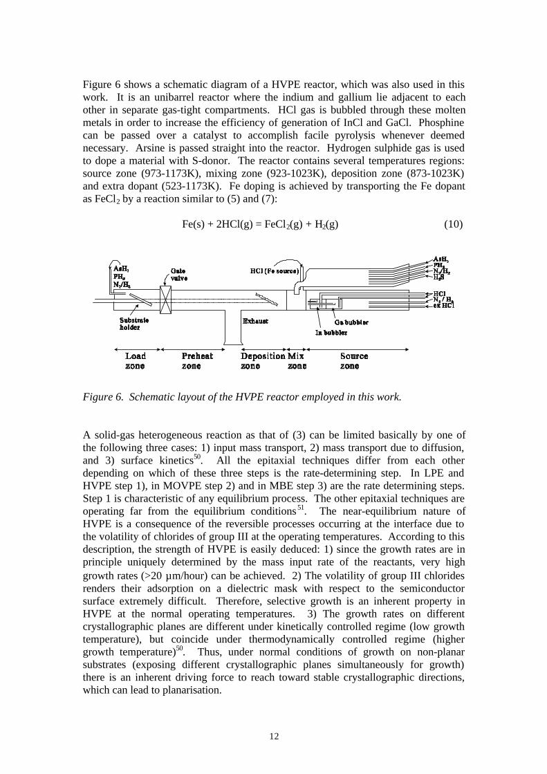
Figure 6 shows a schematic diagram of a HVPE reactor, which was also used in thiswork. It is an unibarrel reactor where the indium and gallium lie adjacent to eachother in separate gas-tight compartments. HCl gas is bubbled through these moltenmetals in order to increase the efficiency of generation of InCl and GaCl. Phosphinecan be passed over a catalyst to accomplish facile pyrolysis whenever deemednecessary. Arsine is passed straight into the reactor. Hydrogen sulphide gas is usedto dope a material with S-donor. The reactor contains several temperatures regions:source zone (973-1173K), mixing zone (923-1023K), deposition zone (873-1023K)and extra dopant (523-1173K). Fe doping is achieved by transporting the Fe dopantas FeCl2 by a reaction similar to (5) and (7):
Fe(s) + 2HCl(g) = FeCl2(g) + H2(g) (10)
Figure 6. Schematic layout of the HVPE reactor employed in this work.
A solid-gas heterogeneous reaction as that of (3) can be limited basically by one ofthe following three cases: 1) input mass transport, 2) mass transport due to diffusion,and 3) surface kinetics50. All the epitaxial techniques differ from each otherdepending on which of these three steps is the rate-determining step. In LPE andHVPE step 1), in MOVPE step 2) and in MBE step 3) are the rate determining steps.Step 1 is characteristic of any equilibrium process. The other epitaxial techniques areoperating far from the equilibrium conditions51. The near-equilibrium nature ofHVPE is a consequence of the reversible processes occurring at the interface due tothe volatility of chlorides of group III at the operating temperatures. According to thisdescription, the strength of HVPE is easily deduced: 1) since the growth rates are inprinciple uniquely determined by the mass input rate of the reactants, very highgrowth rates (>20 µm/hour) can be achieved. 2) The volatility of group III chloridesrenders their adsorption on a dielectric mask with respect to the semiconductorsurface extremely difficult. Therefore, selective growth is an inherent property inHVPE at the normal operating temperatures. 3) The growth rates on differentcrystallographic planes are different under kinetically controlled regime (low growthtemperature), but coincide under thermodynamically controlled regime (highergrowth temperature)50. Thus, under normal conditions of growth on non-planarsubstrates (exposing different crystallographic planes simultaneously for growth)there is an inherent driving force to reach toward stable crystallographic directions,which can lead to planarisation.
13
Despite the upsurge of the MOVPE technology, the selective regrowth of thick layersby this technique has been proved to be not flexible52. Flexible means to achieverapid selective regrowth around etched mesas taller than 4 µm. Although theintroduction of chloride in some chemical form into the MOVPE reactor has resultedin certain improvements concerning the selectivity, a good planarisation and largegrowth rates have not been obtained even in Cl-assisted MOVPE. Good planarisationand perfect selectivity facilitate post processing steps and integration, while high-growth rate is important to avoid dopant redistribution or excessive intermixing ofthin layers in the original structure on which regrowth is carried out53.
High growth rate, perfect selectivity, and good planarisation make HVPE a veryattractive technique to achieve selective and planar regrowth of III-V semiconductorsaround non-planar surfaces in order to fabricate buried-heterostructure laser diodes.
II.4. Semi-insulating III-V materials
Semi-insulating (SI) semiconductors constitute a special class of semiconductormaterials because they possess certain limiting behaviour: they exhibit close to theminimum dark carrier density permissible for a given band gap. The semi-insulatingsemiconductors are valued for their high resistivity, high defect densities, and shortcarrier lifetimes. They provide device isolation for integrated circuits and currentblocking layers for heterostructure lasers.
Semi-insulating bulk III-V semiconductor crystals have long been the mainstay of III-V integrated circuit technology because they replace the function of the oxide insilicon devices to isolate discrete devices or layers within an integrated circuit.Typical examples of SI bulk III-V semiconductors are chromium-doped GaAs(GaAs:Cr) and GaAs compensated by the so-called EL2 defect (GaAs:EL2) as well asiron-doped InP (InP:Fe). Semi-insulating III-V epilayers or heterostructures are usedas high-resistivity insulating or transport blocking layers for electronic andoptoelectronic devices. Examples of SI III-V epilayers are InP:Fe54, iron-dopedGa0.51In0.49P (GaInP:Fe)25, and iron-doped GaAs (GaAs:Fe)28.
In this section, a brief introduction to the deep levels theory and main methods toproduce fully compensated semiconductors is outlined in subsections II.4.1 and II.4.2,respectively. Carrier injection in SI materials is discussed in subsection II.4.3.Finally, subsection II.4.4 describes the main characteristics of the two semi-insulatingmaterials involved in this work: GaInP:Fe and GaAs:Fe.
II.4.1. Deep levels
The presence of crystal defects, surfaces, or dopant atoms leads to the appearance ofenergy levels within the bandgap of a semiconductor. These levels are called shallowif they are near a band edge and deep if they are far (>>kT at 300 K) from the bandedges. At room temperature (RT), shallow impurities are mostly ionised since there isenough thermal energy to make carriers at shallow donor (acceptor) levels jump overthe small energy gap into the conduction (valence) band. In contrast, due to their
14
energy position near the middle of the bandgap, such transition is less probable withthe deep centres (impurities or defects) at RT. However, deep centres may becomeionised by trapping free electrons (holes) from the conduction (valence) band. Deepcentres can be classified according to their charge state. Centres with a neutral andnegatively charged state are called acceptor-like states, whereas centres with a neutraland positively charged state are called donor-like states. Thus, acceptor-like (donor-like) deep centres are neutral in p-type (n-type) semiconductors and ionised in n-type(p-type) semiconductors55.
The probability per unit time kn (kp) that a centre captures an electron (hole) from theconduction (valence) band [and changes its charge state from S (B) to B (S)] isproportional to the concentration n (p) of electrons (holes) in this band:
k c nn n= (11) k c pp p= (12)
where cn and cp are the capture coefficients for electrons and holes, respectively,which can be expressed as:
c vn p n p n p, , ,= σ (13)
where σn and σp are the capture cross sections of electrons and holes, respectively.The larger the carrier capture cross section, the more likely the trapping of that type ofcarrier is to occur. vn and vp are the thermal velocities of electrons and holes,respectively.
Carrier emission from the centre to a band occurs with a probability per unit time gn
(B→S) and gp (S→B) for electrons and holes, respectively. Thus, the changes inconcentration per unit time, or total rates, for the different processes result from theproduct of the probability per unit time (kn, kp, gn, gp) times the concentration s or b ofthe centre in the corresponding initial charge state. The total rates are given by
k s c nsn n= for electron capture g bn for electron emission k b c pbp p= for hole capture g sp for hole emission (14)
At thermal equilibrium, each capture rate kns or kpb is equal to the correspondingemission rate gnb or gps (“principle of detailed balance”56), and the ratio between theunoccupied and the occupied centres is given by:
sb
f Nf N f
E EkT
t t
t t t
T F=−
= − =−
( )exp
1 11 (15)
where Nt (= s + b) is the centre density, ft the occupancy factor of the centre55, ET thedeep energy level, EF the Fermi level, T the temperature and k=8.614x10⁻⁵ eV/K is theBoltzmann’s constant. Thus, applying the “principle of detailed balance” and Eq.(15), the following expressions are obtained for the carrier emission probability:
15
g v NE E
kTv nn n n c
c Tn n= −
−
=σ σexp 1 (16)
g v NE E
kTv pp p p V
v Tp p=
−
=σ σexp 1 (17)
where n1 is the electron concentration when the Fermi level coincides with the energylevel of the centre and p1=ni
2/n1, ni being the intrinsic concentration. Note that fromEq. (15), (16) and (17), ft can be written as
fn v p v
v n n v p ptn n p p
n n p p
=+
+ + +1 1
1 1
σ σ
σ σ( ) ( ) (18)
A centre is classified as a trap if once a carrier is captured at the centre site, thiscarrier stays there until it is reemitted back into the band it comes from. But, if acarrier of opposite sign is trapped on the same site, electron-hole recombinationoccurs (before the first carrier is reemitted), then the centre is classified as arecombination centre. This is mainly a Shockley-Read-Hall (SRH) recombinationprocess (characteristically non-radiative), whose net recombination rate, R, is
R k s g b k b g snp n
n n p pn n p pi
p n
= − = − =−
+ + +( ) ( )
( ) ( )τ τ1 1
(19)
where τn and τp are the minority carrier lifetime of holes and electrons due to thecentre, given by:
τσn p
n p n p tv N,, ,
=1 (20)
Thus, a deep level is characterised by its energy level, ET, and capture cross sections,σe and σh, while the lifetimes, τp and τn, and the density of deep centres, Nt, arematerial parameters.
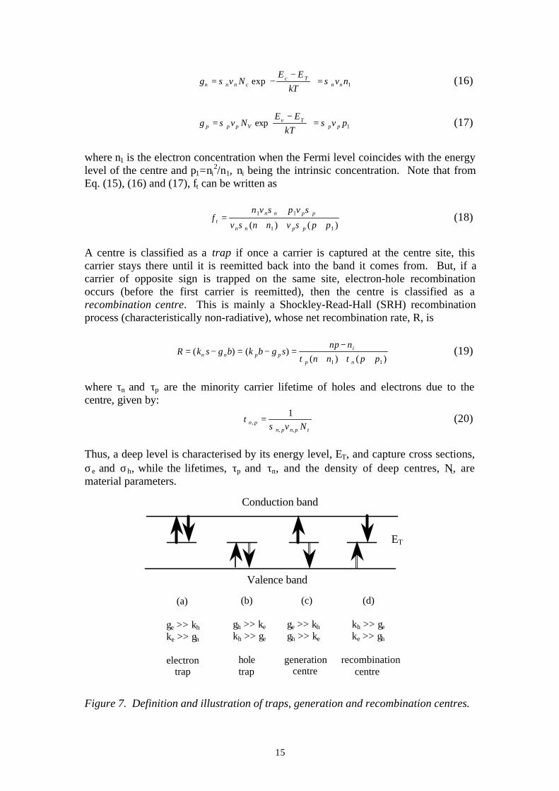
Figure 7. Definition and illustration of traps, generation and recombination centres.
Conduction band
Valence band
(a)
ge >> khke >> gh
electron trap
(b)
gh >> ke kh >> ge
hole trap
(c)
ge >> kh gh >> ke
generation centre
(d)
kh >> ge ke >> gh
recombination centre
ET
16
The condition for a defect or impurity of being an electron trap, a hole trap, arecombination centre, or a generation centre is given by the relative values of ke, kh, ge
and gh, which are functions of the doping concentration, temperature, andcompensation. Figure 7 illustrates the definition of an electron trap (a), hole trap (b),generation centre (c) and recombination centre (d)57. Nevertheless, the name trap isfrequently used to refer to deep levels in general.
II.4.2. Fully compensated III-V semiconductors
Semi-insulating semiconductors are formed when a dominant deep level cancels(compensates) the net charges from other defect and dopant levels. In this way, thefree carrier concentration is reduced and the Fermi level is pinned at an energy nearthe dominant deep level, which can be located anywhere within the band structure.Therefore, in general, a deep level close to the middle of the bandgap is preferred inorder to obtain high resistivity. It must be noticed that fully compensated materialsare sometimes erroneously referred as “intrinsic” because the Fermi level rests nearthe middle of the band gap, as in the textbook case of an ideal intrinsic semiconductorfree of defects. However, since the Fermi level in SI materials is pinned by the highcompensation of donors by acceptors, or vice versa, features as space-charge effectsand carrier lifetimes are far different from those attributed to intrinsicsemiconductors58.
There are basically four methods for creating intentional compensation: A) radiationor implant damage, B) compensation of charge around small metallic precipitates, C)nonstoichiometric growth, and D) doping with impurities to produce known deeplevels.
A) Crystal damage leads to the formation of defects within the semiconductorcharacterised by dangling bonds. As the densities of these deep defects producedby radiation are increased, the Fermi level moves within the band gap, producinghigh resistivity materials. Direct radiation damage can be achieved by proton oroxygen implantation59.
B) Compensation of charge around small metallic precipitates is a less commoncompensation mechanism. Precipitates can be produced through implantation ofmetal ions, followed by annealing, or directly by molecular beam epitaxy at lowsubstrates temperatures followed by annealing. The metal precipitates act asinternal Schottky contacts that deplete charge of either sign in a sphericaldepletion region60.
C) Nonstoichiometric GaAs and related materials have high density of defects suchas gallium vacancies (VGa), arsenic interstitials (Asi), arsenic antisites (AsGa), andarsenic precipitates. For example, low-temperature-grown (LTG) GaAs by MBEat 200-400 °C is nonstoichiometric with an excess of arsenic that is taken up bypoint defects in the as-grown materials61. This is a common method to fabricateSI-GaAs epilayers. SI-GaInP has been also prepared as LTG GaInP by MBE at200 °C [resistivity (ρ) ≈ 4x10⁹ Ωcm]62.
D) It is relatively easy to introduce dopant precursors into the epitaxial growthprocess, making possible to directly grow compensated materials. The mostcommon dopants used for intentional compensation in III-V semiconductors arethe transition metal elements. These impurities, when incorporated
17
substitutionally into the semiconductor host give birth to donor- or acceptor-deeplevels. These are known to occupy the III-sites, i.e., cation sites. Among the deeplevel dopants Fe, Cr, Ti and Ru63,64,65,66 that have been investigated so far in InP,Fe is one of the most extensively studied transition metal dopant. Highresistivities of InP:Fe, approaching 2x10⁸ Ωcm, have been measured67 and InP:Felayers are commonly used as current confinement layers in InP-based buriedheterostructure lasers. In GaAs, the transition elements Fe, Cr and Ti have beenalso studied68,69,70. Ternary and quaternary materials can be made semi-insulatingby using the common deep acceptor Fe as in InP and GaAs. Ga0.47In0.53As:Feexhibits ρ ∼ 103 Ωcm, close to its intrinsic value71. Extremely high ρ values havebeen measured on iron-doped Ga0.51In0.49P grown by HVPE72 as it will be shownin subsection II.4.4. Iron-doped quaternaries GaInAsP and AlGaInAs have beenalso investigated73. In the case of AlGaAs, non-metallic dopants as Ge andoxygen have been used to fabricate semi-insulating AlGaAs layers by LPE andMOVPE, respectively, as current blocking layers in GaAs-based buriedheterostructure lasers74,75. Additional data about type (donor or acceptor), chargestates and energy level of common deep impurities in InP, GaAs and GaP can befound in Ref. 58 and 76.
II.4.3. Carrier injection in SI materials
To exemplify the discussion on carrier injection in trap-controlled insulators, SI-InP:Fe will be used since it has been extensively studied, and it can be generalised toother SI materials. Substitutional Fe in InP (Eg = 1.35 eV) provides a deep acceptorlevel at Ec-0.6 eV 63, i.e., very near the middle of the bandgap. This deep acceptorlevel compensates background shallow donors by trapping the electrons and therebylowering the thermal electron concentration. In this way, the trapped negative chargeopposes further electron injection. Thus, the material remains highly resistive underlow and moderate electron injection. But when the voltage is further increased, abreakdown voltage is reached and the current rises significantly. According toLampert and Mark theory77, this breakdown voltage (Vb) corresponds to the trap-filledregime (that is, all the traps are filled and injected carriers go increasingly into theconduction band) and its value is given by
V e N N db
t d=−( ) 2
2ε (21)
where Nt is the total Fe trap concentration, ε the dielectric constant of InP, e thefundamental charge, d the thickness of the semi-insulating layer, and Nd is thebackground shallow donor concentration (filled trap density at equilibrium).Nevertheless, Lampert and Mark’s simplified theory does not consider certain factorssuch as diffusion effects, generation/recombination processes, drift velocity saturationand impact ionisation that can affect the breakdown voltage and, in general, thecurrent-voltage (I-V) behaviour of SI structures78. For example, if the InP:Fe layer isvery thin in a n/SI/n structure, carrier diffusion effects at the interfaces may make thislayer ineffective for current blocking. This is not due to the bulk properties of theInP:Fe layer but to the behaviour of the n/SI/n configuration.
18
If instead of electrons, holes are injected in a p/InP:Fe/p structure, its I-V behaviourwill be different from that of the n/InP:Fe/n configuration79. Still, the p/SI/p structureexhibits high resistivity, although not because of hole trapping, since Fe is mainly anelectron trap, but due to the structure itself with the Fermi level in the upper half ofthe bandgap. In addition, this fact also leads to a decrease of the p/SI/p resistivity asthe Fe concentration increases, opposite to the n/SI/n structure.
Finally, when holes are injected into the InP:Fe material in a n/InP:Fe/p configuration,they recombine with electrons which have been trapped by deep-level centres,resulting in the removal of the barrier to electron injection. In this way, both electronsand holes are injected into the SI material. This phenomenon is called “doubleinjection”80. Thus, under double injection, the semi-insulating behaviour as expectedof a deep level dopant is not retained and hence significant current can flow throughthis material. As it will be seen in Part III, double injection in the SI burying layer ofa BH-laser is a cause of leakage current.
II.4.4. Semi-insulating Ga0.51In0.49P:Fe and GaAs:Fe
A) SI-GaInP:Fe
So far, Fe doped GaInP has been obtained by LPE81 and HVPE25. Active ironoccupies the III-group site and introduces a deep acceptor level at 0.74 eV above thevalence band81. The empty state, the neutral charge state, is Fe3+, and the filled one,the negatively charged state, is Fe2+.
The carrier capture cross sections of Fe in GaInP have been studied by severalauthors. Cesna et al.82 measured the electron capture cross section at differenttemperatures by time-resolved photoluminescence (TR-PL), obtaining a value of σn inthe range from 6x10-16 to 1x10-15 cm2 for the temperature interval 70-250 K.Takanohashi et al.81 measured a value of 3.4x10⁻¹³ cm2 for the hole capture crosssection (σp) by deep-level transient spectroscopy (DLTS). Before the capture of anelectron, the defect is in the neutral Fe3+ state with no long-range potential, whilebefore the capture of a hole, the defect is in the Fe2+ state of charge –1, leading to along-range attractive potential. It is thus reasonable that σh > σe.
Lourdudoss et al.72 characterised the I-V-T behaviour of n-GaAs/GaInP:Fe/n-GaAsstructures prepared by HVPE, demonstrating for the first time the semi-insulatingnature of GaInP:Fe. Fig. 8 shows the resistivity at 0.1 V bias of GaInP:Fe as afunction of the total Fe concentration (measured by secondary ion mass spectroscopy(SIMS)) at various temperatures. It is seen that the resistivity varies with the total Feconcentration ([FeSIMS]) reaching a maximum value at [FeSIMS] ≈ 4x1017 cm-3. It isremarkable that GaInP:Fe exhibits extremely high values of the resistivity (I-V curvescould not be obtained below 398 K due to the very high resistance of the samples).This fact is of great importance in the fabrication of both electronic and optoelectronicdevices.
The aforementioned authors also indicated the existence of interstitial Fe atoms andFeP precipitates, besides site-incorporated Fe, in GaInP:Fe grown by HVPE. Thismeans that the active Fe concentration (site-incorporated Fe), which provides the SI
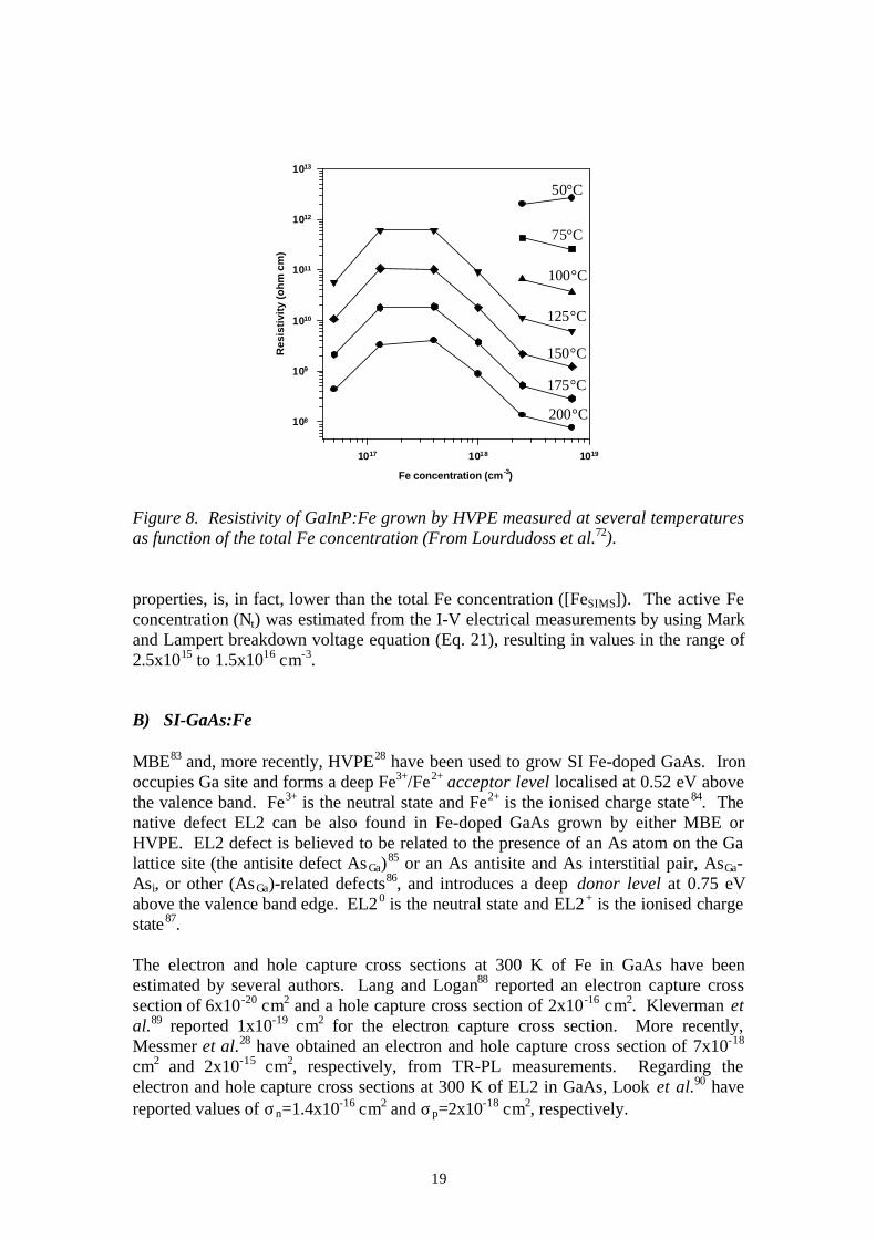
19
Fe concentration (cm -3)
1017 1018 1019
Res
isti
vity
(oh
m c
m)
108
109
1010
1011
1012
1013
Figure 8. Resistivity of GaInP:Fe grown by HVPE measured at several temperaturesas function of the total Fe concentration (From Lourdudoss et al.72).
properties, is, in fact, lower than the total Fe concentration ([FeSIMS]). The active Feconcentration (Nt) was estimated from the I-V electrical measurements by using Markand Lampert breakdown voltage equation (Eq. 21), resulting in values in the range of2.5x1015 to 1.5x1016 cm-3.
B) SI-GaAs:Fe
MBE83 and, more recently, HVPE28 have been used to grow SI Fe-doped GaAs. Ironoccupies Ga site and forms a deep Fe3+/Fe2+ acceptor level localised at 0.52 eV abovethe valence band. Fe3+ is the neutral state and Fe2+ is the ionised charge state 84. Thenative defect EL2 can be also found in Fe-doped GaAs grown by either MBE orHVPE. EL2 defect is believed to be related to the presence of an As atom on the Galattice site (the antisite defect AsGa)85 or an As antisite and As interstitial pair, AsGa-Asi, or other (AsGa)-related defects86, and introduces a deep donor level at 0.75 eVabove the valence band edge. EL20 is the neutral state and EL2+ is the ionised chargestate87.
The electron and hole capture cross sections at 300 K of Fe in GaAs have beenestimated by several authors. Lang and Logan88 reported an electron capture crosssection of 6x10-20 cm2 and a hole capture cross section of 2x10-16 cm2. Kleverman etal.89 reported 1x10-19 cm2 for the electron capture cross section. More recently,Messmer et al.28 have obtained an electron and hole capture cross section of 7x10-18
cm2 and 2x10-15 cm2, respectively, from TR-PL measurements. Regarding theelectron and hole capture cross sections at 300 K of EL2 in GaAs, Look et al.90 havereported values of σn=1.4x10⁻¹⁶ cm2 and σp=2x10-18 cm2, respectively.
50°C
75°C
100°C
125°C
150°C
175°C
200°C
20
1016 1017 1018 101 9 102 0 1021
107
108
109
1010
1011
Res
istiv
ity (
Ω c
m)
Iron concentration (cm -3)
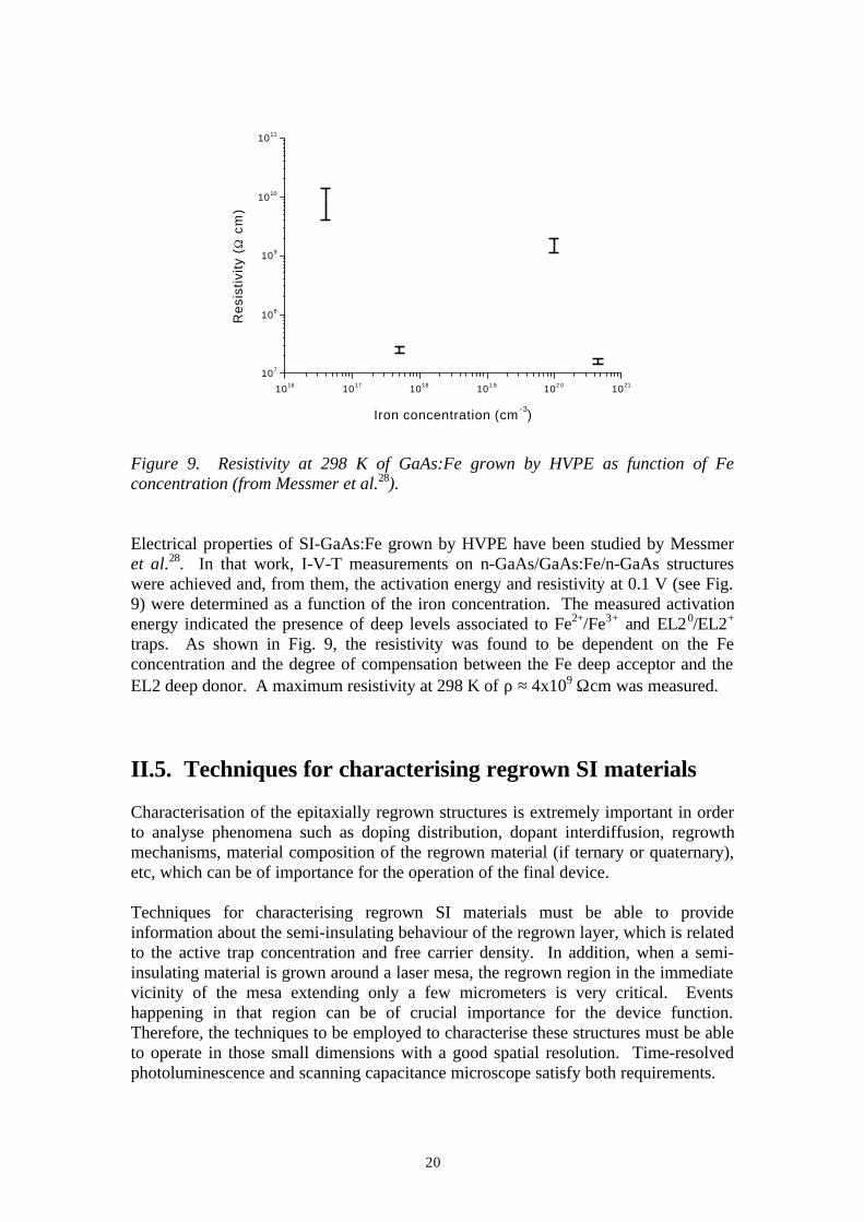
Figure 9. Resistivity at 298 K of GaAs:Fe grown by HVPE as function of Feconcentration (from Messmer et al.28).
Electrical properties of SI-GaAs:Fe grown by HVPE have been studied by Messmeret al.28. In that work, I-V-T measurements on n-GaAs/GaAs:Fe/n-GaAs structureswere achieved and, from them, the activation energy and resistivity at 0.1 V (see Fig.9) were determined as a function of the iron concentration. The measured activationenergy indicated the presence of deep levels associated to Fe2+/Fe3+ and EL20/EL2+
traps. As shown in Fig. 9, the resistivity was found to be dependent on the Feconcentration and the degree of compensation between the Fe deep acceptor and theEL2 deep donor. A maximum resistivity at 298 K of ρ ≈ 4x10⁹ Ωcm was measured.
II.5. Techniques for characterising regrown SI materials
Characterisation of the epitaxially regrown structures is extremely important in orderto analyse phenomena such as doping distribution, dopant interdiffusion, regrowthmechanisms, material composition of the regrown material (if ternary or quaternary),etc, which can be of importance for the operation of the final device.
Techniques for characterising regrown SI materials must be able to provideinformation about the semi-insulating behaviour of the regrown layer, which is relatedto the active trap concentration and free carrier density. In addition, when a semi-insulating material is grown around a laser mesa, the regrown region in the immediatevicinity of the mesa extending only a few micrometers is very critical. Eventshappening in that region can be of crucial importance for the device function.Therefore, the techniques to be employed to characterise these structures must be ableto operate in those small dimensions with a good spatial resolution. Time-resolvedphotoluminescence and scanning capacitance microscope satisfy both requirements.
21
II.5.1. Time-resolved photoluminescence (TR-PL)
TR-PL is a contact-less and non-destructive technique with a capability to measurevery short trapping times. It is a direct method to study the carrier trapping since thedecay of the luminescence measured at the bandgap energy is determined by thecarrier transfer from the extended band states to the localised states in the trappingcentres.
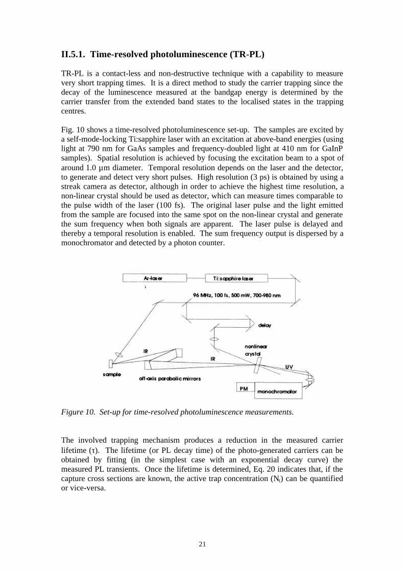
Fig. 10 shows a time-resolved photoluminescence set-up. The samples are excited bya self-mode-locking Ti:sapphire laser with an excitation at above-band energies (usinglight at 790 nm for GaAs samples and frequency-doubled light at 410 nm for GaInPsamples). Spatial resolution is achieved by focusing the excitation beam to a spot ofaround 1.0 µm diameter. Temporal resolution depends on the laser and the detector,to generate and detect very short pulses. High resolution (3 ps) is obtained by using astreak camera as detector, although in order to achieve the highest time resolution, anon-linear crystal should be used as detector, which can measure times comparable tothe pulse width of the laser (100 fs). The original laser pulse and the light emittedfrom the sample are focused into the same spot on the non-linear crystal and generatethe sum frequency when both signals are apparent. The laser pulse is delayed andthereby a temporal resolution is enabled. The sum frequency output is dispersed by amonochromator and detected by a photon counter.
Figure 10. Set-up for time-resolved photoluminescence measurements.
The involved trapping mechanism produces a reduction in the measured carrierlifetime (τ). The lifetime (or PL decay time) of the photo-generated carriers can beobtained by fitting (in the simplest case with an exponential decay curve) themeasured PL transients. Once the lifetime is determined, Eq. 20 indicates that, if thecapture cross sections are known, the active trap concentration (Nt) can be quantifiedor vice-versa.
22
In addition to the deep level-related information, this technique as a typical PLcharacterisation, can also provide information related to the energy bandgap of theexcited material, such as alloy composition and ordering effect91.
Thus, the small dimensions of the excitation spot over the sample (∼1 µm diameter)allow achieving a PL mapping of the analysed surface (e.g. a cleaved surfaceperpendicular to mesa stripes) in order to provide valuable information about spatialdistribution of traps (e.g. active Fe distribution in regrown Fe-doped layers aroundlaser mesas92), besides material composition and/or ordering in alloys.
II.5.2. Scanning capacitance microscopy (SCM)
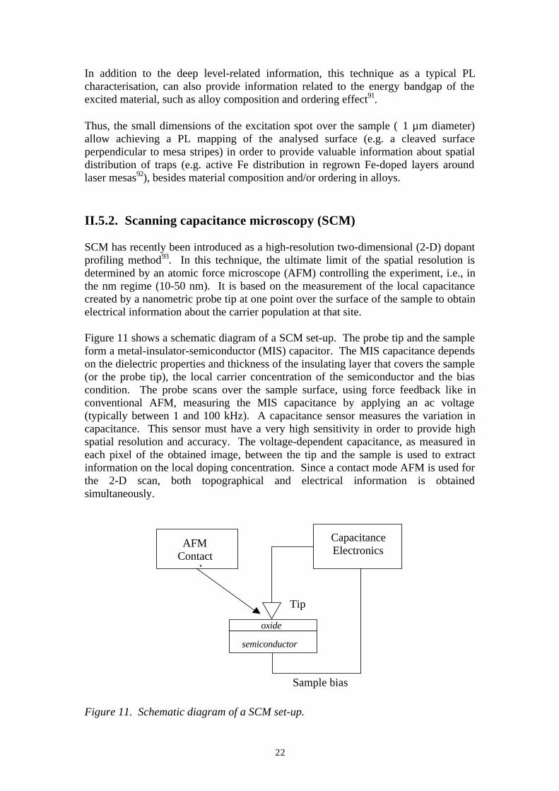
SCM has recently been introduced as a high-resolution two-dimensional (2-D) dopantprofiling method93. In this technique, the ultimate limit of the spatial resolution isdetermined by an atomic force microscope (AFM) controlling the experiment, i.e., inthe nm regime (10-50 nm). It is based on the measurement of the local capacitancecreated by a nanometric probe tip at one point over the surface of the sample to obtainelectrical information about the carrier population at that site.
Figure 11 shows a schematic diagram of a SCM set-up. The probe tip and the sampleform a metal-insulator-semiconductor (MIS) capacitor. The MIS capacitance dependson the dielectric properties and thickness of the insulating layer that covers the sample(or the probe tip), the local carrier concentration of the semiconductor and the biascondition. The probe scans over the sample surface, using force feedback like inconventional AFM, measuring the MIS capacitance by applying an ac voltage(typically between 1 and 100 kHz). A capacitance sensor measures the variation incapacitance. This sensor must have a very high sensitivity in order to provide highspatial resolution and accuracy. The voltage-dependent capacitance, as measured ineach pixel of the obtained image, between the tip and the sample is used to extractinformation on the local doping concentration. Since a contact mode AFM is used forthe 2-D scan, both topographical and electrical information is obtainedsimultaneously.
Figure 11. Schematic diagram of a SCM set-up.
AFMContactmode
CapacitanceElectronics
Tip
oxide
semiconductor
Sample bias
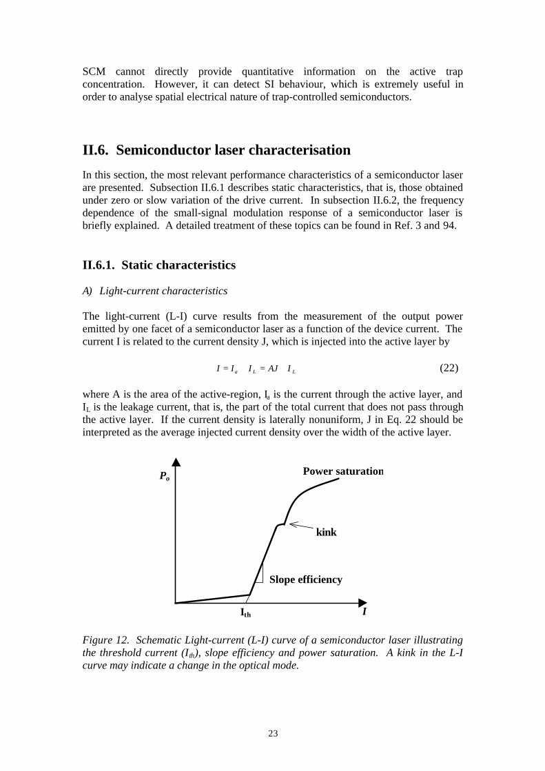
23
SCM cannot directly provide quantitative information on the active trapconcentration. However, it can detect SI behaviour, which is extremely useful inorder to analyse spatial electrical nature of trap-controlled semiconductors.
II.6. Semiconductor laser characterisation
In this section, the most relevant performance characteristics of a semiconductor laserare presented. Subsection II.6.1 describes static characteristics, that is, those obtainedunder zero or slow variation of the drive current. In subsection II.6.2, the frequencydependence of the small-signal modulation response of a semiconductor laser isbriefly explained. A detailed treatment of these topics can be found in Ref. 3 and 94.
II.6.1. Static characteristics
A) Light-current characteristics
The light-current (L-I) curve results from the measurement of the output poweremitted by one facet of a semiconductor laser as a function of the device current. Thecurrent I is related to the current density J, which is injected into the active layer by
I I I AJ Ia L L= + = + (22)
where A is the area of the active-region, Ia is the current through the active layer, andIL is the leakage current, that is, the part of the total current that does not pass throughthe active layer. If the current density is laterally nonuniform, J in Eq. 22 should beinterpreted as the average injected current density over the width of the active layer.
Figure 12. Schematic Light-current (L-I) curve of a semiconductor laser illustratingthe threshold current (Ith), slope efficiency and power saturation. A kink in the L-Icurve may indicate a change in the optical mode.
I
Po
Ith
kink
Slope efficiency
Power saturation
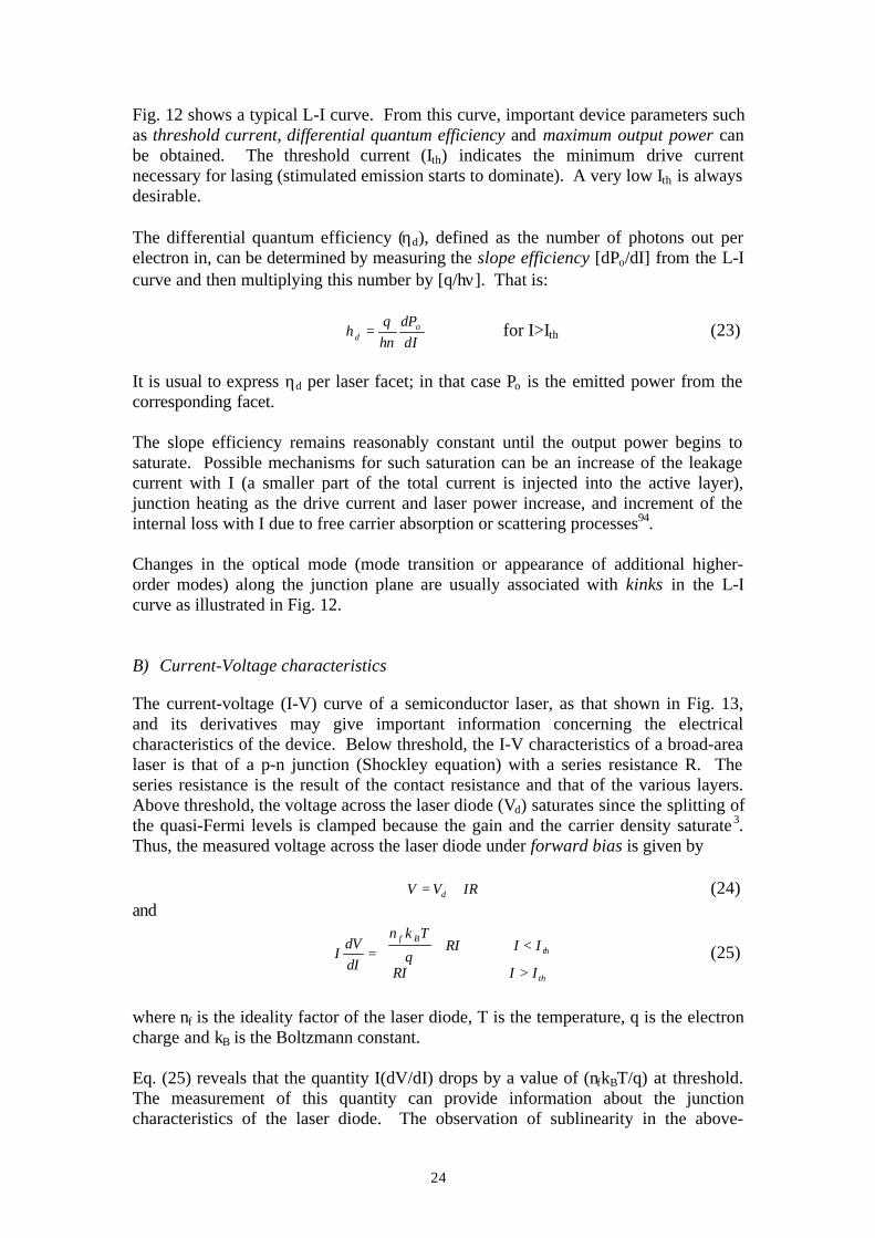
24
Fig. 12 shows a typical L-I curve. From this curve, important device parameters suchas threshold current, differential quantum efficiency and maximum output power canbe obtained. The threshold current (Ith) indicates the minimum drive currentnecessary for lasing (stimulated emission starts to dominate). A very low Ith is alwaysdesirable.
The differential quantum efficiency (ηd), defined as the number of photons out perelectron in, can be determined by measuring the slope efficiency [dPo/dI] from the L-Icurve and then multiplying this number by [q/hν]. That is:
ηνd
oqh
dPdI
= for I>Ith (23)
It is usual to express ηd per laser facet; in that case Po is the emitted power from thecorresponding facet.
The slope efficiency remains reasonably constant until the output power begins tosaturate. Possible mechanisms for such saturation can be an increase of the leakagecurrent with I (a smaller part of the total current is injected into the active layer),junction heating as the drive current and laser power increase, and increment of theinternal loss with I due to free carrier absorption or scattering processes94.
Changes in the optical mode (mode transition or appearance of additional higher-order modes) along the junction plane are usually associated with kinks in the L-Icurve as illustrated in Fig. 12.
B) Current-Voltage characteristics
The current-voltage (I-V) curve of a semiconductor laser, as that shown in Fig. 13,and its derivatives may give important information concerning the electricalcharacteristics of the device. Below threshold, the I-V characteristics of a broad-arealaser is that of a p-n junction (Shockley equation) with a series resistance R. Theseries resistance is the result of the contact resistance and that of the various layers.Above threshold, the voltage across the laser diode (Vd) saturates since the splitting ofthe quasi-Fermi levels is clamped because the gain and the carrier density saturate3.Thus, the measured voltage across the laser diode under forward bias is given by
V V IRd= + (24)and
IdVdI
n k T
qRI I I
RI I I
f Bth
th
= + <
>
(25)
where nf is the ideality factor of the laser diode, T is the temperature, q is the electroncharge and kB is the Boltzmann constant.
Eq. (25) reveals that the quantity I(dV/dI) drops by a value of (nfkBT/q) at threshold.The measurement of this quantity can provide information about the junctioncharacteristics of the laser diode. The observation of sublinearity in the above-
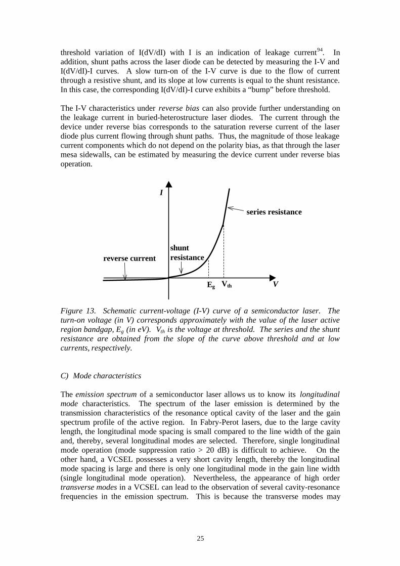
25
threshold variation of I(dV/dI) with I is an indication of leakage current94. Inaddition, shunt paths across the laser diode can be detected by measuring the I-V andI(dV/dI)-I curves. A slow turn-on of the I-V curve is due to the flow of currentthrough a resistive shunt, and its slope at low currents is equal to the shunt resistance.In this case, the corresponding I(dV/dI)-I curve exhibits a “bump” before threshold.
The I-V characteristics under reverse bias can also provide further understanding onthe leakage current in buried-heterostructure laser diodes. The current through thedevice under reverse bias corresponds to the saturation reverse current of the laserdiode plus current flowing through shunt paths. Thus, the magnitude of those leakagecurrent components which do not depend on the polarity bias, as that through the lasermesa sidewalls, can be estimated by measuring the device current under reverse biasoperation.
Figure 13. Schematic current-voltage (I-V) curve of a semiconductor laser. Theturn-on voltage (in V) corresponds approximately with the value of the laser activeregion bandgap, Eg (in eV). Vth is the voltage at threshold. The series and the shuntresistance are obtained from the slope of the curve above threshold and at lowcurrents, respectively.
C) Mode characteristics
The emission spectrum of a semiconductor laser allows us to know its longitudinalmode characteristics. The spectrum of the laser emission is determined by thetransmission characteristics of the resonance optical cavity of the laser and the gainspectrum profile of the active region. In Fabry-Perot lasers, due to the large cavitylength, the longitudinal mode spacing is small compared to the line width of the gainand, thereby, several longitudinal modes are selected. Therefore, single longitudinalmode operation (mode suppression ratio > 20 dB) is difficult to achieve. On theother hand, a VCSEL possesses a very short cavity length, thereby the longitudinalmode spacing is large and there is only one longitudinal mode in the gain line width(single longitudinal mode operation). Nevertheless, the appearance of high ordertransverse modes in a VCSEL can lead to the observation of several cavity-resonancefrequencies in the emission spectrum. This is because the transverse modes may
V
I
Eg Vth
series resistance
reverse currentshuntresistance
26
modify spatially the effective index of the structure allowing different resonanceconditions (frequencies).
The spatial-mode characteristics of a semiconductor laser are characterised by the so-called near field and far field. The spatial-intensity distribution of the emitted lightnear the laser facet is known as the near field. In general, several transverse andlateral modes may appear, and the resulting near field is formed by a superposition ofthem. However, the active layer dimension is chosen in such a way that only thelowest-order transverse and lateral modes are supported by the waveguide. In thiscase the near field exhibits a Gaussian distribution, showing the shape of a singleelliptical spot in IPLs or a circular spot in circular VCSELs. The full widths at halfmaximum (FWHM), along the two axis of an elliptical spot or along the diameter of acircular one, are taken to be a measure of the spot.
The angular intensity distribution far from the laser facet is known as the far field.The far-field patterns indicate the angular spread of the laser mode and are importantin determining the coupling efficiency between the semiconductor laser and an opticalfiber. Mathematically the far-field pattern is obtained by taking the two-dimensionalFourier transform of the near field. The angles corresponding to the lateral andtransverse directions taken at the FWHM (beam divergence) are used as a measure ofthe angular spread of the emitted light.
Both near and far fields depend on the guiding mechanism. Thus, for strongly index-guided lasers, the near field is largely confined within the active layer95, while, incontrast, the lateral near field for gain-guided lasers extends considerably beyond theoxide window width94. In general, strong index antiguiding produces wide far-field29,gain-guiding structures exhibit twin-lobe far fields96, and with strong index-guidingnarrow far-fields are obtained97. Therefore, the near field and far- field can be used todetermine the optical guiding mechanism in semiconductor lasers.
II.6.2. Dynamic characteristics
The output power of a semiconductor laser can be modulated directly by modulatingthe excitation current. The analysis of its modulation properties allows us todetermine its feasibility to be used as light source for high-speed data transmissionsystems. Particularly, the small-signal modulation analysis is useful for predicting theparameter dependence94. In this analysis, the modulation current is made up of dc(>Ith) and small amplitude ac components. A typical frequency dependence of thesmall-signal modulation response of a single-mode semiconductor laser is shown inFig. 14, where ω=2πf, f being the frequency of the ac component. The 3-dB small-signal modulation bandwidth (f3dB) is defined as the modulation frequency at whichthe laser response has dropped 3 dB (one half) with respect to its value at lowfrequencies. f3dB represents the practical modulation bandwidth of the semiconductorlaser before the output signal is degraded. The modulation response (transferfunction) of a single-mode semiconductor laser can be modelled as3:
H fAe
f f j jf f
j
r p
d
( )(( ) )( )
=− + +
ωτ
γπ
2 2
2
(26)
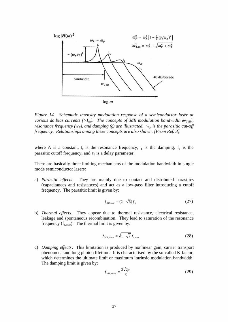
27
Figure 14. Schematic intensity modulation response of a semiconductor laser atvarious dc bias currents (>Ith). The concepts of 3dB modulation bandwidth (ω3dB),resonance frequency (ωR), and damping (γ) are illustrated. ωp is the parasitic cut-offfrequency. Relationships among these concepts are also shown. [From Ref. 3]
where A is a constant, fr is the resonance frequency, γ is the damping, fp is theparasitic cutoff frequency, and τd is a delay parameter.
There are basically three limiting mechanisms of the modulation bandwidth in singlemode semiconductor lasers:
a) Parasitic effects. They are mainly due to contact and distributed parasitics(capacitances and resistances) and act as a low-pass filter introducing a cutofffrequency. The parasitic limit is given by:
f fdB par p3 2 3, ( )= + (27)
b) Thermal effects. They appear due to thermal resistance, electrical resistance,leakage and spontaneous recombination. They lead to saturation of the resonancefrequency (fr,max). The thermal limit is given by:
f fdB therm r3 1 2, ,max= + (28)
c) Damping effects. This limitation is produced by nonlinear gain, carrier transportphenomena and long photon lifetime. It is characterised by the so-called K-factor,which determines the ultimate limit or maximum intrinsic modulation bandwidth.The damping limit is given by:
fKdB damp3
2 2, = π (29)
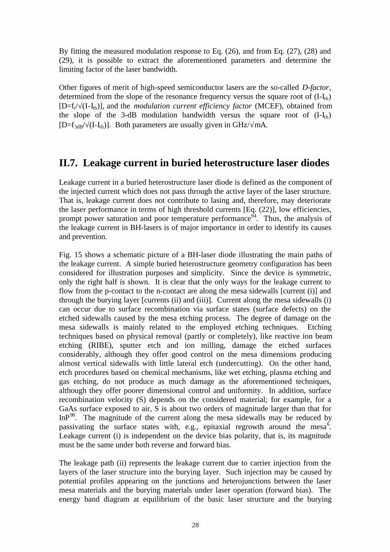
28
By fitting the measured modulation response to Eq. (26), and from Eq. (27), (28) and(29), it is possible to extract the aforementioned parameters and determine thelimiting factor of the laser bandwidth.
Other figures of merit of high-speed semiconductor lasers are the so-called D-factor,determined from the slope of the resonance frequency versus the square root of (I-Ith)[D=fr/√(I-Ith)], and the modulation current efficiency factor (MCEF), obtained fromthe slope of the 3-dB modulation bandwidth versus the square root of (I-Ith)[D=f3dB/√(I-Ith)]. Both parameters are usually given in GHz/√mA.
II.7. Leakage current in buried heterostructure laser diodes
Leakage current in a buried heterostructure laser diode is defined as the component ofthe injected current which does not pass through the active layer of the laser structure.That is, leakage current does not contribute to lasing and, therefore, may deterioratethe laser performance in terms of high threshold currents [Eq. (22)], low efficiencies,prompt power saturation and poor temperature performance94. Thus, the analysis ofthe leakage current in BH-lasers is of major importance in order to identify its causesand prevention.
Fig. 15 shows a schematic picture of a BH-laser diode illustrating the main paths ofthe leakage current. A simple buried heterostructure geometry configuration has beenconsidered for illustration purposes and simplicity. Since the device is symmetric,only the right half is shown. It is clear that the only ways for the leakage current toflow from the p-contact to the n-contact are along the mesa sidewalls [current (i)] andthrough the burying layer [currents (ii) and (iii)]. Current along the mesa sidewalls (i)can occur due to surface recombination via surface states (surface defects) on theetched sidewalls caused by the mesa etching process. The degree of damage on themesa sidewalls is mainly related to the employed etching techniques. Etchingtechniques based on physical removal (partly or completely), like reactive ion beametching (RIBE), sputter etch and ion milling, damage the etched surfacesconsiderably, although they offer good control on the mesa dimensions producingalmost vertical sidewalls with little lateral etch (undercutting). On the other hand,etch procedures based on chemical mechanisms, like wet etching, plasma etching andgas etching, do not produce as much damage as the aforementioned techniques,although they offer poorer dimensional control and uniformity. In addition, surfacerecombination velocity (S) depends on the considered material; for example, for aGaAs surface exposed to air, S is about two orders of magnitude larger than that forInP98. The magnitude of the current along the mesa sidewalls may be reduced bypassivating the surface states with, e.g., epitaxial regrowth around the mesa6.Leakage current (i) is independent on the device bias polarity, that is, its magnitudemust be the same under both reverse and forward bias.
The leakage path (ii) represents the leakage current due to carrier injection from thelayers of the laser structure into the burying layer. Such injection may be caused bypotential profiles appearing on the junctions and heterojunctions between the lasermesa materials and the burying materials under laser operation (forward bias). Theenergy band diagram at equilibrium of the basic laser structure and the burying
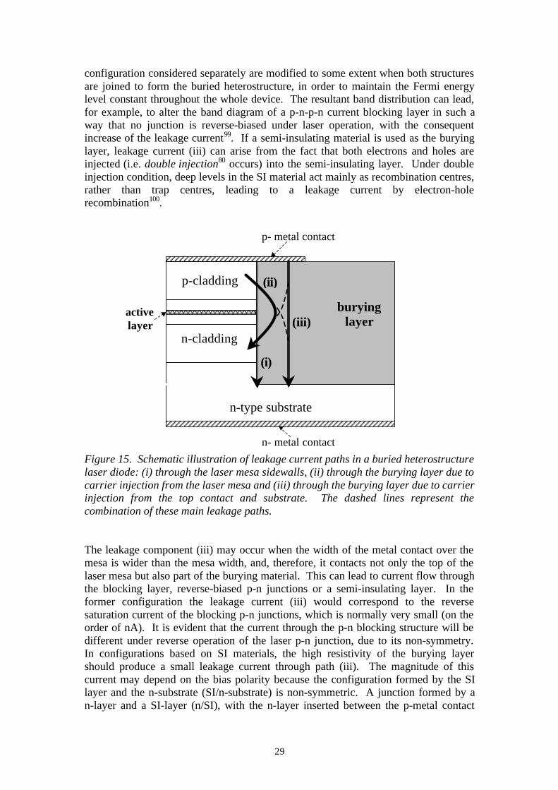
29
configuration considered separately are modified to some extent when both structuresare joined to form the buried heterostructure, in order to maintain the Fermi energylevel constant throughout the whole device. The resultant band distribution can lead,for example, to alter the band diagram of a p-n-p-n current blocking layer in such away that no junction is reverse-biased under laser operation, with the consequentincrease of the leakage current99. If a semi-insulating material is used as the buryinglayer, leakage current (iii) can arise from the fact that both electrons and holes areinjected (i.e. double injection80 occurs) into the semi-insulating layer. Under doubleinjection condition, deep levels in the SI material act mainly as recombination centres,rather than trap centres, leading to a leakage current by electron-holerecombination100.
Figure 15. Schematic illustration of leakage current paths in a buried heterostructurelaser diode: (i) through the laser mesa sidewalls, (ii) through the burying layer due tocarrier injection from the laser mesa and (iii) through the burying layer due to carrierinjection from the top contact and substrate. The dashed lines represent thecombination of these main leakage paths.
The leakage component (iii) may occur when the width of the metal contact over themesa is wider than the mesa width, and, therefore, it contacts not only the top of thelaser mesa but also part of the burying material. This can lead to current flow throughthe blocking layer, reverse-biased p-n junctions or a semi-insulating layer. In theformer configuration the leakage current (iii) would correspond to the reversesaturation current of the blocking p-n junctions, which is normally very small (on theorder of nA). It is evident that the current through the p-n blocking structure will bedifferent under reverse operation of the laser p-n junction, due to its non-symmetry.In configurations based on SI materials, the high resistivity of the burying layershould produce a small leakage current through path (iii). The magnitude of thiscurrent may depend on the bias polarity because the configuration formed by the SIlayer and the n-substrate (SI/n-substrate) is non-symmetric. A junction formed by an-layer and a SI-layer (n/SI), with the n-layer inserted between the p-metal contact
buryinglayer
n-type substrate
n-cladding
p-cladding
(i)
(ii)
(iii)
p- metal contact
n- metal contact
activelayer

30
and the SI layer, can be also used in order to reduce even more the current path(iii)100. The purpose of the n-layer is to block hole injection from the p-contact intothe SI material in order to avoid double injection. In this case, leakage current (iii)would correspond to that flowing through a n/SI/n-substrate structure, which isusually highly resistive72,100, although, as in the previous cases, its magnitude may bedependent on the bias polarity if the geometry of the configuration is not symmetric.
It is obvious that current paths resulting from the combination of the aforementionedbasic leakage paths may also occur (e.g., dashed lines in Fig. 15), especially in thenear vicinity of the laser mesa where the energy band bending may be considerable.As mentioned in the previous section, experimental estimation of the magnitude andorigin of the leakage current in a semiconductor laser may be revealed by measuringits I-V curve. Nevertheless, to determine the main leakage paths and their causes in aBH laser can be a complicated task, even in simple geometries as that illustrated inFig. 15, especially in the presence of layers of different material composition anddoping in a two-dimensional (2-D) distribution. The use of 2-D device simulators hasbeen shown to be a very useful tool for this purpose99,100.
31
III. ORIGINAL WORK
The development of the thesis is presented in this part. The purpose here has been toshow and discuss the most significant results published in the appended papers in acoherent manner, so that the reader can follow the evolution of the work fromepitaxial growth to device simulation, passing through materials and devicecharacterisation. Additional comments to the experiments and results not included inthe papers are also presented.
Each section of this part describes the achievement of each of the four aims of thethesis mentioned in the introduction. Section III.1 (associated to paper A) presentsthe development of a suitable, reliable and reproducible technique to achieve selectiveepitaxial regrowth of semi-insulating materials around high Al-containingGaAs/AlGaAs laser mesas by HVPE, overcoming the major problem due to Aloxidation, as well as regrowth morphological characteristics. In section III.2, buriedheterostructures with semi-insulating materials are characterised by optical (TR-PL)(paper B and C) and electrical (SCM) (paper D) characterisation techniques in orderto provide relevant information regarding the properties of regrown SI layers andregrowth-related features. The performance of fabricated BH lasers, static (paper E,F and G) and dynamic (paper H) characteristics, is presented and discussed in sectionIII.3. Analysis of the leakage current in BH lasers with SI-GaInP blocking layer bycomputer simulation is described in section III.4 (paper I), fulfilling the last of theaims. Finally, conclusions and suggestions for future research are outlined in sectionIII.5.
III.1. Epitaxial regrowth around Al-containing laser mesas
This is probably the most important section of the thesis since all the followingsections are based on this. First, growth and properties of GaInP and GaAs layers onplanar GaAs substrates and regrowth experiments achieved on non-planar GaAssubstrates carried out by HVPE are presented in subsection III.1.1. Subsection III.1.2shows results on regrowth around GaAs/AlGaAs laser mesas by using several Al-oxide removal methods, explaining their characteristics and reasons which led to thefinal method: HCl-based in-situ cleaning. Subsection III.1.3 provides a qualitativeexplanation of the operation of the HCl gas-based in-situ cleaning technique. Finally,morphology and mechanisms of GaInP and GaAs regrowth are discussed insubsection III.1.4.
Regrowth experiments were achieved in the HVPE reactor described in subsectionII.3.2 and shown schematically in Fig. 6, at atmospheric pressure in an ambient ofnitrogen.
III.1.1. GaInP and GaAs layers properties
Layers of GaInP and GaAs were epitaxially grown on planar GaAs substrates byHVPE in order to calibrate and determine electrical properties of the materialsintended for regrowth.
32
Undoped layers of GaInP were grown on (100) SI-GaAs substrates at different growthtemperatures, obtaining the best surface morphology at 700 °C. Using this growthtemperature, the GaInP composition was calibrated by modifying the pGa/(pGa+pIn)ratio, pGa and pIn being the partial pressures of GaCl and InCl, respectively. Thecomposition was chosen according to the work reported by Hoshino et al.101. Theseauthors showed that the crystal quality of GaInP grown by Cl-VPE at atmosphericpressure is better when GaInP is lattice matched to GaAs at the growth temperaturethan at room temperature. Applying this, the lattice mismatch value at roomtemperature corresponding to lattice match at our growth temperature of 700 °C isequal to +950 ppm102 (the sign “+” indicates that the composition of GaInP lies on theInP side). Thus, the HCl gas flow rates through Ga and In were adjusted in order toobtain a lattice mismatch value at RT in the range from zero to +950 ppm. Inparticular, the material was considered optimised for a lattice mismatch, measured byhigh resolution X-ray diffraction (HRXRD), of +855 ppm, which corresponds to50.45% of Ga [Eg=1.874 eV at RT (Eq. 2)]. The flow rates were 1.9 sccm, 11 sccmand 225 sccm for GaCl, InCl and PH3 (30% in hydrogen), respectively, which leads toa V/III ratio of 5.2. The growth rate was ∼12 µm/h. Room temperature Hallmeasurements achieved on 2 µm thick undoped GaInP layers revealed a n-typeresidual concentration of ∼3x1015 cm-3, resistivity of ∼0.5 Ωcm, and Hall mobility of∼3900 cm2/Vs. Hoshino and co-workers obtained for undoped Ga0.52In0.48P grown bychloride vapour phase epitaxy a background carrier concentration of 1x1015 cm-3 andmobility around 2000 cm2/Vs. The high value of the mobility in our samplesindicates good quality material.
The growth parameters for Fe-doped GaInP were the same as those for undopedGaInP but with additional HCl flow (0.9 sccm) over solid Fe during growth. The totaliron concentration was measured by SIMS. The resistivity of n-GaAs/GaInP:Fe/n-GaAs structures as a function of the total iron concentration is shown in Fig. 8. Adetailed description about growth and characterisation can be found in Ref. 72 and102.
Sulfur-doped GaInP layers were also grown by HVPE and characterized by Halleffect in order to determine the electrical properties of n-type GaInP, which wasintended to use in a n-GaInP/GaInP:Fe structure as burying configuration in BHlasers. The growth parameters were the same as those for undoped GaInP growth butwith additional H2S (200 ppm in H2) gas flow (195 sccm). The measured electronconcentration, resistivity and Hall mobility at room temperature were ∼3x1018 cm-3,∼5x10⁻³ Ωcm and ∼490 cm2/Vs, respectively.
Undoped GaAs layers were grown at a growth temperature of 735 °C, with flow ratesof 2.5 sccm and 180 sccm for GaCl (pure HCl through Ga) and AsH3 (5% inhydrogen), respectively, which corresponds to a V/III ratio of 3.6. The growth ratewas ∼ 4 µm/h. Room temperature Hall measurements on 2 µm thick GaAs layersgrown on SI-GaAs indicated a n-type background concentration of ∼ 1x1015 cm-3,resistivity of ∼ 1.0 Ωcm, and Hall mobility of ∼ 5100 cm2/Vs.
The procedure to calibrate Fe-doped GaAs was similar to that realised on GaInP:Fe.Details about characterisation procedures and results are reported by Messmer et al.28.
33
The measured resistivity of n-GaAs/GaAs:Fe/n-GaAs planar configurations versus thetotal iron concentration is shown in Fig. 9.
Prior to the intended regrowth of the aforementioned materials around Al-containinglaser structures, regrowth experiments around non-planar GaAs substrates werecarried out for testing purposes. Fig. 16 shows two examples of epitaxial growtharound non-planar substrates achieved by HVPE, illustrating the strength of thistechnique described in subsection II.3.2. The silicon nitride etch mask used tofabricate the non-planar structures was also employed during regrowth. In Fig. 16A,GaInP has been selectively regrown around wet etched 5.5-µm tall mesa stripes alongthe [110] direction on a GaAs (001) substrate. It is seen that no growth has takenplace on the silicon nitride mask and planarisation is remarkable despite theconsiderable height of the mesa. The growth time was 10 minutes. Fig. 16.B showsalso a non-planar GaAs (001) substrate with GaInP regrowth by HVPE, but in thiscase growth has been achieved inside the wet etched 7.5-µm deep grooves along the[110] direction. It is also observed that GaInP has grown selectively inside the deepgroove and not over the mask. The growth time was 12 minutes. In both cases, theexcessive growth time allows observing the formation of (111)B planes (consisting ofonly phosphorous atoms) above the non-planar structures. 111 planes are verystable due to their lowest surface energy50. During HVPE growth under an excessPH3 or AsH3 atmosphere, (111)B has been found to be more stable than (111)Aplanes (consisting of only III-group atoms), as Fig. 16A and 16B corroborate.
A)
B)
Figure 16. Selective epitaxial regrowth of GaInP by hydride vapour phase epitaxyaround [110] directional wet etched mesa stripes (A) and grooves (B). (111)Bcrystallographic planes appear on excessive regrowth.
_[110]
[001]
[110]
_[110]
[001]
[110]
(111)B
(111)B
34
III.1.2. Al-oxide cleaning procedures
As mentioned in the introduction, the major problem to epitaxial growth around Al-containing structures is the exposure of the Al-containing surfaces to the atmosphereafter mesa etching since aluminium oxide is formed very quickly. Al-oxide is atenacious oxide, which acts as a mask preventing regrowth due to the high selectivityof the HVPE technique. Therefore, an oxide cleaning procedure must be achievedbefore regrowth in order to remove Al-oxide and other oxides and contaminants fromthe etching process.
GaAs/AlGaAs laser mesas fabricated for the regrowth experiments (details on thelaser structure and mesa fabrication can be found in paper A) were etched through theactive layer down to the GaAs substrate in order to obtain an Al-free planar surfacebetween mesas. This was achieved with the purpose of avoiding an excessive area ofAl-containing material susceptible to oxidation. In this way, the only etched surfaceswhere Al-oxidation may occur are those on the sidewalls of the mesa with Al-containing layers in the laser structure.
A) Conventional wet cleaning procedures
First attempts to make regrowth around wet etched GaAs/AlGaAs IPL mesas wereconducted by using conventional wet cleaning methods just after mesa etching. Wetcleaning procedures were based on bases and acids. In particular, ammoniumhydroxide (NH4OH) 25 % and hydrochloric acid (HCl) 37% solutions, typically usedfor oxide removal in GaAs43, were considered. The wet cleaning time ranged from 2to 5 min. These solutions practically do not etch GaAs but their oxides and Al-containing materials. On the other hand, the etching of Al-oxide depends on thephase exhibited by this material. Al-oxide (Al2O3) can present distinct phases:amorphous (ρ), cubic (χ, γ), cubic spinel (η), orthorhombic (κ), monoclinic (θ) andrhombohedral (α-alumina)103. α-alumina is the most stable phase; it resists hydrationand attack by acids. However this phase is usually formed at high temperatures andhence its formation is unlikely under our operating conditions. Usually, oxidesformed in aqueous solutions or by air exposure are mainly non-stoichiometric, oftenhave non-reproducible compositions and can readily incorporate impurities. Thus, itis more probable to find more reactive phases like amorphous, hydrated oxides and γ-Al2O3 104,105. Thus, if we consider the most stable of these three phases, γ-Al2O3, thefollowing reactions may occur
Al2O3 (γ) + 3NH4OH(aq) = 2Al(OH)3 (aq) + 3NH3 (aq) (30)and Al2O3 (γ) + 6HCl(aq) = 2AlCl3 (aq) + 3H2O (31)
when NH4OH and HCl are used, respectively. The calculated free energy change(∆G) at 25 °C associated to reactions (30) and (31) is ∆G30 = -14.11 kJ and ∆G31 =-118.8 kJ, respectively. In both cases ∆G < 0, that is, both reactions occurspontaneously towards the consumption of γ-Al2O3. Therefore, according to theassumed chemical reactions, both wet cleanings would be effective in removing γ-
35
Al2O3 and, therefore, the other less stable possible phases. On the other hand, it isalso reasonable to expect a chemical etching of Al-containing materials by theaforementioned etchants as the following reactions suggest:
AlAs + 3NH4OH (aq) = Al(OH)3 (aq) + AsH3 + 3NH3 (aq) (32)and AlAs + 3HCl (aq) = AlCl3 (aq) + AsH3 (33)
with ∆G32 = -289.54 kJ and ∆G33 = -301.27 kJ, respectively, at 25 °C. In this way,Al-oxide would be lifted off by the etched mesa material.
In any case, whether the native Al-oxide removal mechanism is by direct Al-oxideetching or by Al(Ga)As etching, if the wet cleaning is followed by an aqueouscleaning treatment, the surfaces would oxidise again. Because of this, after wetcleaning, the samples were rinsed in propanol instead of water. In spite of thispreventive measure, even if N2 is blown during the loading of the sample inside theloading zone of the HVPE reactor, air exposure occurs unavoidably for a short time (afew seconds).
Figure 17. Regrowth of GaInP:Fe around a GaAs/AlGaAs IPL mesa cleaned withammonium hydroxide for 5 min before regrowth. Regrowth has taken place only onthe non- or low aluminium containing materials.
Figure 17 illustrates a typical GaInP:Fe regrowth experiment after a conventional wetAl-oxide removal method. The cleaning sequence after mesa formation and beforeloading was: ammonium hydroxide for 5 minutes, rinsing in propanol twice and N2
blowing. It is seen that GaInP:Fe has grown on Al-free surfaces, such as the GaAssubstrate and the p-GaAs contact layer, and around the low Al-content active region.Nevertheless, there is no growth around the Al0.6Ga0.4As cladding layers. Such aselective growth is a clear indication that a layer of Al-oxide exists on theAl0.6Ga0.4As cladding surfaces, which acts as a mask (similar to the top silicon nitridemask) avoiding growth on it. It is interesting to observe the appearance of stable111B planes at the edges of the oxidised surfaces similar to the case of excessivegrowth in GaAs non-planar structures (Fig. 16). Regrowth around dry etched circularVCSEL mesas also led to irregular interfaces with voids. It is therefore evident thateven if the wet cleaning removes Al-oxide from the mesa sidewalls, the exposure toair during the loading operation leads to Al-oxide formation, which remains duringthe regrowth process. This fact also indicates that, unlike Ga- and As- oxides105, Al-
36
oxide is not eliminated by desorption at temperatures as high as 705 °C and 740 °C(pre-heat temperatures for GaInP and GaAs regrowth, respectively).
B) HCl in-situ etching
To circumvent the above problem, a different approach was adopted. Since Al-oxideis formed inevitably during the loading operation and is not desorbed during the pre-heat operation (705 °C or 740 °C for 3 minutes), it appears that such oxide should beremoved inside the HVPE growth chamber, where there is no oxygen at all, justbefore regrowth. To this end, a slight etching of the mesa sidewalls by usinghydrogen chloride gas at the growth temperature (700 °C or 735 °C) in the HVPEgrowth zone was attempted. Hereafter, this procedure will be referred to as HCl in-situ etching. When this procedure was adopted, no other wet chemical treatment wasemployed before loading the etched mesas in the reactor.
The HCl in-situ etching was achieved by introducing pure HCl gas and GaCl (HClthrough Ga) at a flow rate of 0.6 sccm and 1.9 sccm, respectively. The reason foradding GaCl was based on previous experiments on in-situ etching of InP in ourHVPE reactor106. Those experiments revealed that the addition of InCl during HClgas etching suppressed to some extent the vertical etching rate. In this way, a similarbehaviour was expected to occur on in-situ etching of GaAs-based materials. Sinceour purpose was to etch only the sidewalls of the mesa, GaCl would lead to a moreefficient lateral etching. In order to etch slightly the mesa sidewalls short etchingtimes were used because excessive times may produce a high lateral etching thatwould modify considerably the mesa shape and dimensions. In addition, as a result ofthe HCl gas etching of AlGaAs materials, aluminium chloride is generated [seereaction (33)], which can etch the quartz (SiO2) walls of the growth chamber. For theetching times used in our experiments, 30 and 45 seconds, no noticeable etching ofquartz walls took place.
Regrowth results after in-situ etching were similar to those obtained by using only wetchemical cleaning methods. An example of a typical regrowth experiment is shownin Fig. 18. In this case, regrowth of GaInP was achieved around wet etched VCSEL
Figure 18. Regrowth of GaInP:Fe around a GaAs/AlGaAs VCSEL mesa treated withHCl in-situ etching before regrowth. No prior wet chemical cleaning based on acidsor bases was used.
n-GaAs substrate
GaInP
VCSEL
mesaGaInP
SiNx mask
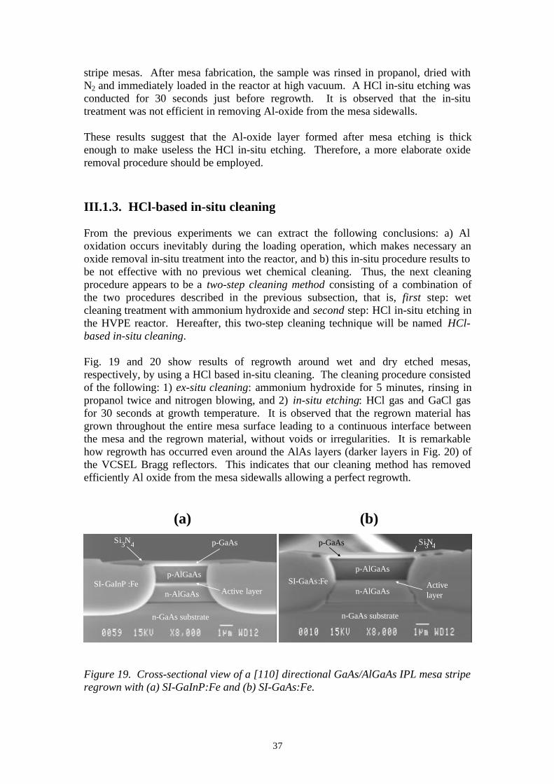
37
stripe mesas. After mesa fabrication, the sample was rinsed in propanol, dried withN2 and immediately loaded in the reactor at high vacuum. A HCl in-situ etching wasconducted for 30 seconds just before regrowth. It is observed that the in-situtreatment was not efficient in removing Al-oxide from the mesa sidewalls.
These results suggest that the Al-oxide layer formed after mesa etching is thickenough to make useless the HCl in-situ etching. Therefore, a more elaborate oxideremoval procedure should be employed.
III.1.3. HCl-based in-situ cleaning
From the previous experiments we can extract the following conclusions: a) Aloxidation occurs inevitably during the loading operation, which makes necessary anoxide removal in-situ treatment into the reactor, and b) this in-situ procedure results tobe not effective with no previous wet chemical cleaning. Thus, the next cleaningprocedure appears to be a two-step cleaning method consisting of a combination ofthe two procedures described in the previous subsection, that is, first step: wetcleaning treatment with ammonium hydroxide and second step: HCl in-situ etching inthe HVPE reactor. Hereafter, this two-step cleaning technique will be named HCl-based in-situ cleaning.
Fig. 19 and 20 show results of regrowth around wet and dry etched mesas,respectively, by using a HCl based in-situ cleaning. The cleaning procedure consistedof the following: 1) ex-situ cleaning: ammonium hydroxide for 5 minutes, rinsing inpropanol twice and nitrogen blowing, and 2) in-situ etching: HCl gas and GaCl gasfor 30 seconds at growth temperature. It is observed that the regrown material hasgrown throughout the entire mesa surface leading to a continuous interface betweenthe mesa and the regrown material, without voids or irregularities. It is remarkablehow regrowth has occurred even around the AlAs layers (darker layers in Fig. 20) ofthe VCSEL Bragg reflectors. This indicates that our cleaning method has removedefficiently Al oxide from the mesa sidewalls allowing a perfect regrowth.
(a) (b)
Figure 19. Cross-sectional view of a [110] directional GaAs/AlGaAs IPL mesa striperegrown with (a) SI-GaInP:Fe and (b) SI-GaAs:Fe.
SI- GaInP :Fe
n-GaAs substrate
n-AlGaAs
p-AlGaAs
Active layer
Si3N4 p-GaAs
SI-GaAs:Fe
n-GaAs substrate
n-AlGaAs
p-AlGaAs
Activelayer
p-GaAs Si3N4
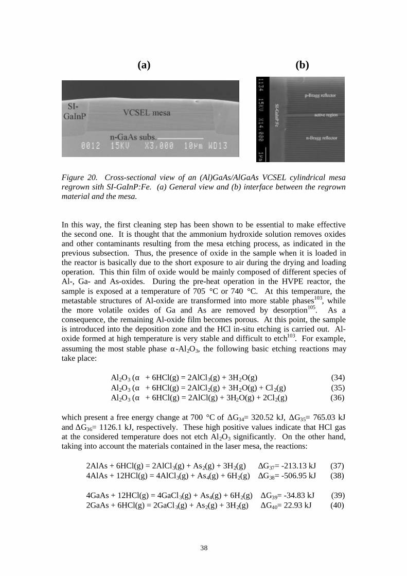
38
(a) (b)
Figure 20. Cross-sectional view of an (Al)GaAs/AlGaAs VCSEL cylindrical mesaregrown sith SI-GaInP:Fe. (a) General view and (b) interface between the regrownmaterial and the mesa.
In this way, the first cleaning step has been shown to be essential to make effectivethe second one. It is thought that the ammonium hydroxide solution removes oxidesand other contaminants resulting from the mesa etching process, as indicated in theprevious subsection. Thus, the presence of oxide in the sample when it is loaded inthe reactor is basically due to the short exposure to air during the drying and loadingoperation. This thin film of oxide would be mainly composed of different species ofAl-, Ga- and As-oxides. During the pre-heat operation in the HVPE reactor, thesample is exposed at a temperature of 705 °C or 740 °C. At this temperature, themetastable structures of Al-oxide are transformed into more stable phases103, whilethe more volatile oxides of Ga and As are removed by desorption105. As aconsequence, the remaining Al-oxide film becomes porous. At this point, the sampleis introduced into the deposition zone and the HCl in-situ etching is carried out. Al-oxide formed at high temperature is very stable and difficult to etch103. For example,assuming the most stable phase α-Al2O3, the following basic etching reactions maytake place:
Al2O3 (α) + 6HCl(g) = 2AlCl3(g) + 3H2O(g) (34)Al2O3 (α) + 6HCl(g) = 2AlCl2(g) + 3H2O(g) + Cl2(g) (35)Al2O3 (α) + 6HCl(g) = 2AlCl(g) + 3H2O(g) + 2Cl2(g) (36)
which present a free energy change at 700 °C of ∆G34= 320.52 kJ, ∆G35= 765.03 kJand ∆G36= 1126.1 kJ, respectively. These high positive values indicate that HCl gasat the considered temperature does not etch Al2O3 significantly. On the other hand,taking into account the materials contained in the laser mesa, the reactions:
2AlAs + 6HCl(g) = 2AlCl3(g) + As2(g) + 3H2(g) ∆G37= -213.13 kJ (37)4AlAs + 12HCl(g) = 4AlCl3(g) + As4(g) + 6H2(g) ∆G38= -506.95 kJ (38)
4GaAs + 12HCl(g) = 4GaCl3(g) + As4(g) + 6H2(g) ∆G39= -34.83 kJ (39)2GaAs + 6HCl(g) = 2GaCl3(g) + As2(g) + 3H2(g) ∆G40= 22.93 kJ (40)
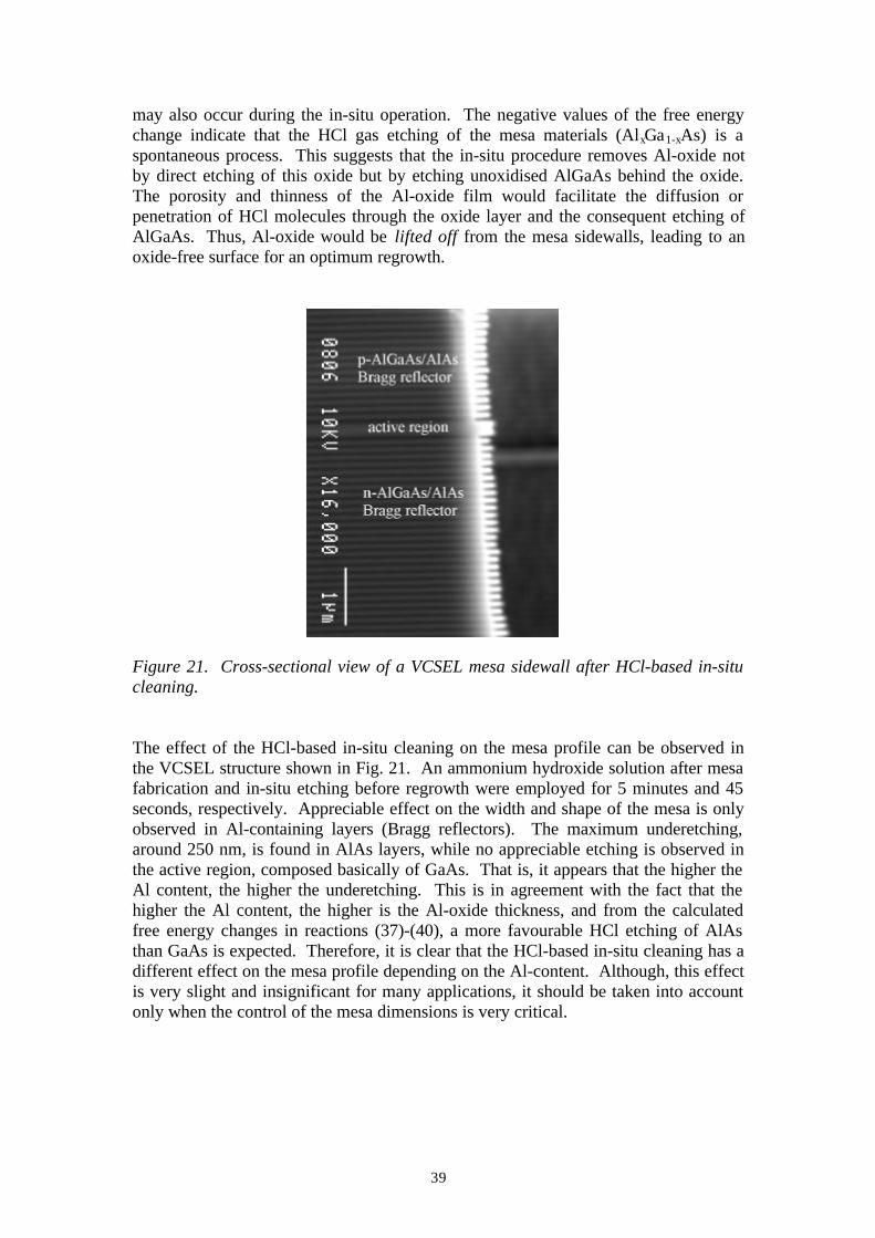
39
may also occur during the in-situ operation. The negative values of the free energychange indicate that the HCl gas etching of the mesa materials (AlxGa1-xAs) is aspontaneous process. This suggests that the in-situ procedure removes Al-oxide notby direct etching of this oxide but by etching unoxidised AlGaAs behind the oxide.The porosity and thinness of the Al-oxide film would facilitate the diffusion orpenetration of HCl molecules through the oxide layer and the consequent etching ofAlGaAs. Thus, Al-oxide would be lifted off from the mesa sidewalls, leading to anoxide-free surface for an optimum regrowth.
Figure 21. Cross-sectional view of a VCSEL mesa sidewall after HCl-based in-situcleaning.
The effect of the HCl-based in-situ cleaning on the mesa profile can be observed inthe VCSEL structure shown in Fig. 21. An ammonium hydroxide solution after mesafabrication and in-situ etching before regrowth were employed for 5 minutes and 45seconds, respectively. Appreciable effect on the width and shape of the mesa is onlyobserved in Al-containing layers (Bragg reflectors). The maximum underetching,around 250 nm, is found in AlAs layers, while no appreciable etching is observed inthe active region, composed basically of GaAs. That is, it appears that the higher theAl content, the higher the underetching. This is in agreement with the fact that thehigher the Al content, the higher is the Al-oxide thickness, and from the calculatedfree energy changes in reactions (37)-(40), a more favourable HCl etching of AlAsthan GaAs is expected. Therefore, it is clear that the HCl-based in-situ cleaning has adifferent effect on the mesa profile depending on the Al-content. Although, this effectis very slight and insignificant for many applications, it should be taken into accountonly when the control of the mesa dimensions is very critical.

40
III.1.4. Regrowth morphology
Figure 22A and 22B illustrate planarisation features of the GaInP:Fe and GaAs:Feregrowth, respectively, on [110] directional wet etched laser mesa stripes. It is seenthat in each case the morphology is different. GaInP:Fe regrowth provides goodplanarisation in the close vicinity of the mesa with a decrease of the regrown layerthickness farther away from the mesa, reaching a constant thickness of ∼2 µm. Theregrowth morphology obtained in these experiments is similar to that reported byLourdudoss et al.25 on GaInP regrowth on non-planar GaAs (100) substrates (dryetched mesa stripes) by HVPE. In a related work by Holtz102, time resolved regrowthof GaInP around [110] directional dry etched mesas suggested a similar regrowthsequence as that found in the InP:Fe regrowth by HVPE on InP mesas along the samedirection107. That is, at the first stage of regrowth 111B planes emerge immediatelydue to their stability, and further growth seemed to occur mainly from (001) plane andlittle on the 111B planes. Thus, during regrowth high index hhlplanes, resultingfrom the combination of 001 and 110, with l/h ≤ 3 are formed and, as the growthprogresses, the tendency to planarise increases by the emergence of hhlwith l/h ≥ 3,leading to a regrowth morphology as that seen in Fig. 22A. It can be thought that inorder to increase the lateral growth (planarisation) along the [110] direction a longerregrowth time could be employed; but, such increment on the growth time does notresult in a significant improvement of the planarisation but in overgrowth above themesa brink, as shown in Fig. 16A, producing the appearance of stable 111B planeswhich take the shape of a funnel. It is interesting to observe that the silicon nitridemask overhang resulting from the mesa wet etching fabrication provides planarisationin the immediate vicinity of the mesa, stopping planes such as 111B on the mesabrink and enhancing the growth from the (001) plane. However, an excessiveregrowth leads unavoidably to the formation of 111B planes above the mask edges(see Fig. 16). Although, even with an excessive growth, the material does not tend togrow on the mask over the mesa, such overgrowth makes further processing difficult(e.g. for photolithography). In any case, the thickness of the regrown GaInP:Fe layeraround the laser mesas can be considered sufficient to fabricate BH-lasers; in high-speed designs the width of the top metal contact over the laser mesa can be madesmall and to lie under the thick part of the regrown GaInP:Fe, close to the mesa, tominimise the parasitics.
Figure 22. SEM cross-sectional view of wet etched mesas with (A) GaInP:Fe and (B)GaAs:Fe regrowth.
41
On the other hand, it is remarkable that a perfect planarisation between the mesas isobtained in the GaAs:Fe regrowth case. Unlike InP regrowth, to the knowledge of theauthor, studies on regrowth sequence of GaAs by HVPE are scarce108. Althoughdetailed experimental and theoretical studies on regrowth profiles of GaAs by HVPEare beyond the scope of this thesis, the present experiments reveal importantinformation related to the regrowth mechanism. The planar morphology seen in Fig.22B suggests that the regrowth mechanism of GaAs:Fe is not the same as thatproposed for GaInP:Fe under the growth conditions considered in these experiments.This is corroborated in Fig. 23 and 24. Fig. 23a and 23b show a [110] directionalGaAs/AlGaAs mesa with GaInP regrown for 10 min and GaAs regrown for 30 min,respectively. Fig. 24a and 24b show GaAs regrown for 15 min on a [110] directionalwet etched AlGaAs stripe mesa and for 20 min around a dry etched stripe GaAs mesaalong the same direction, respectively. In all cases the regrowth time was interruptedbefore expected planarisation was reached. It is seen that while GaInP seems tofollow the regrowth mechanism explained previously, GaAs regrowth exhibits adifferent behaviour. At an early growth stage (Fig. 23b) GaAs has grown on twodifferent regions, on the (100) plane, wetting the bottom part of the mesa (n-claddinglayer), and locally on the top p-cladding layer forming nearly 110 planes. Aftersome time of regrowth (Fig. 24a), both regions become joined, and it is observed thatthe growth rate along the [110] direction is practically negligible. GaAs regrowthexperiment conducted on [110] directional dry etched GaAs mesas108, Fig. 24b, showsthat apparently regrowth took place basically from the (001) plane, and not on the(110) planes. In both cases of regrowth on wet and dry etched mesas, the growthrate was the same as that on planar substrate. These facts indicate that regrowth takesplace mainly on the (100) plane, suggesting that, under the considered regrowthconditions, (110) planes are stable and much more lethargic for further growth thanthe (100) plane. This would explain the appearance of regrown material on the toppart of the wet etched mesa sidewall. Regrowth on the non-vertical wet etched topmesa sidewalls occurs until stable (110) planes are formed, while regrowth on thebottom part of the mesa is decided upon the extent of cooperation between (111) and(001) leading to high index hhl planes in the beginning of regrowth. On the otherhand, dry etched GaAs stripe mesa sidewalls form already (110) planes and,therefore, regrowth on these surfaces does not occur. The fact that the growth ratebecomes isotropic except in the stable [110] direction suggests an enhanced lateraldiffusion of the reactants which overwhelms the orientation dependence of the surfacereaction. Higher surface diffusion length indicates that the atoms are incorporatedfurther away from the mesa sidewalls after their arrival to the surface of the mask.This MOCVD-like behaviour of GaAs regrowth109 could be related to the low growthrate and high growth temperature conditions, which enhance surface diffusion. Sincelow growth rate on planar surfaces is due to low bulk diffusion (diffusion through thediffusion boundary layer) coefficients it is thought that GaAs regrowth would belimited by bulk diffusion of the reactants rather than surface reaction, whereas in theregrowth of GaInP the surface reaction limited growth would dominate. Tateno etal.109 demonstrated that the regrowth mechanism of GaInP by MOCVD can bechanged from GaAs VPE-type (surface reaction limited) to GaAs MOCVD-type(reactants diffusion limited) by either increasing the growth temperature or decreasingthe V/III ratio. Those studies suggest that by adjusting the aforementioned regrowthparameters the regrowth of GaInP by HVPE may exhibit a GaAs-like growthbehaviour, leading to total planarisation.
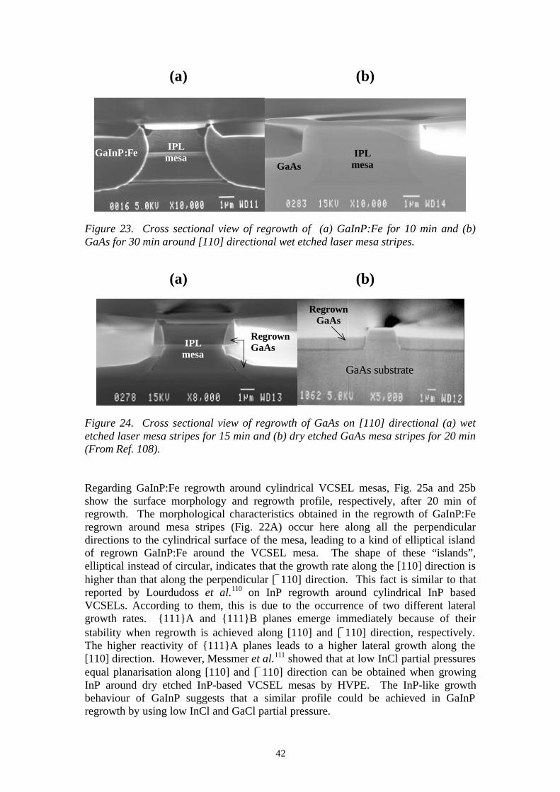
42
(a) (b)
Figure 23. Cross sectional view of regrowth of (a) GaInP:Fe for 10 min and (b)GaAs for 30 min around [110] directional wet etched laser mesa stripes.
(a) (b)
Figure 24. Cross sectional view of regrowth of GaAs on [110] directional (a) wetetched laser mesa stripes for 15 min and (b) dry etched GaAs mesa stripes for 20 min(From Ref. 108).
Regarding GaInP:Fe regrowth around cylindrical VCSEL mesas, Fig. 25a and 25bshow the surface morphology and regrowth profile, respectively, after 20 min ofregrowth. The morphological characteristics obtained in the regrowth of GaInP:Feregrown around mesa stripes (Fig. 22A) occur here along all the perpendiculardirections to the cylindrical surface of the mesa, leading to a kind of elliptical islandof regrown GaInP:Fe around the VCSEL mesa. The shape of these “islands”,elliptical instead of circular, indicates that the growth rate along the [110] direction ishigher than that along the perpendicular [110] direction. This fact is similar to thatreported by Lourdudoss et al.110 on InP regrowth around cylindrical InP basedVCSELs. According to them, this is due to the occurrence of two different lateralgrowth rates. 111A and 111B planes emerge immediately because of theirstability when regrowth is achieved along [110] and [110] direction, respectively.The higher reactivity of 111A planes leads to a higher lateral growth along the[110] direction. However, Messmer et al.111 showed that at low InCl partial pressuresequal planarisation along [110] and [110] direction can be obtained when growingInP around dry etched InP-based VCSEL mesas by HVPE. The InP-like growthbehaviour of GaInP suggests that a similar profile could be achieved in GaInPregrowth by using low InCl and GaCl partial pressure.
IPLmesaGaInP:Fe IPL
mesa GaAs
IPLmesa
GaAs substrate
RegrownGaAs
RegrownGaAs
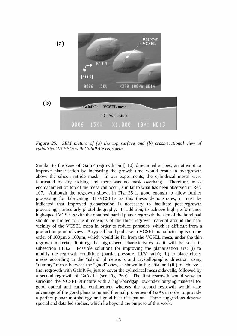
43
Figure 25. SEM picture of (a) the top surface and (b) cross-sectional view ofcylindrical VCSELs with GaInP:Fe regrowth.
Similar to the case of GaInP regrowth on [110] directional stripes, an attempt toimprove planarisation by increasing the growth time would result in overgrowthabove the silicon nitride mask. In our experiments, the cylindrical mesas werefabricated by dry etching and there was no mask overhang. Therefore, maskencroachment on top of the mesa can occur, similar to what has been observed in Ref.107. Although the regrowth shown in Fig. 25 is good enough to allow furtherprocessing for fabricating BH-VCSELs as this thesis demonstrates, it must beindicated that improved planarisation is necessary to facilitate post-regrowthprocessing, particularly photolithography. In addition, to achieve high performancehigh-speed VCSELs with the obtained partial planar regrowth the size of the bond padshould be limited to the dimensions of the thick regrown material around the nearvicinity of the VCSEL mesa in order to reduce parastics, which is difficult from aproduction point of view. A typical bond pad size in VCSEL manufacturing is on theorder of 100µm x 100µm, which would lie far from the VCSEL mesa, under the thinregrown material, limiting the high-speed characteristics as it will be seen insubsection III.3.2. Possible solutions for improving the planarisation are: (i) tomodify the regrowth conditions (partial pressure, III/V ratio); (ii) to place closermesas according to the “island” dimensions and crystallographic direction, using“dummy” mesas between the “good” ones, as shown in Fig. 26a; and (iii) to achieve afirst regrowth with GaInP:Fe, just to cover the cylindrical mesa sidewalls, followed bya second regrowth of GaAs:Fe (see Fig. 26b). The first regrowth would serve tosurround the VCSEL structure with a high-bandgap low-index burying material forgood optical and carrier confinement whereas the second regrowth would takeadvantage of the good planarising and thermal properties of GaAs in order to providea perfect planar morphology and good heat dissipation. These suggestions deservespecial and detailed studies, which lie beyond the purpose of this work.
[011]
[11 0]
RegrownVCSEL
(b)VCSEL mesaGaInP:Fe
n-GaAs substrate
(a)
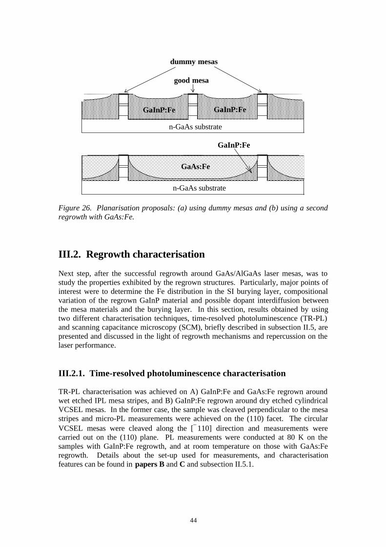
44
Figure 26. Planarisation proposals: (a) using dummy mesas and (b) using a secondregrowth with GaAs:Fe.
III.2. Regrowth characterisation
Next step, after the successful regrowth around GaAs/AlGaAs laser mesas, was tostudy the properties exhibited by the regrown structures. Particularly, major points ofinterest were to determine the Fe distribution in the SI burying layer, compositionalvariation of the regrown GaInP material and possible dopant interdiffusion betweenthe mesa materials and the burying layer. In this section, results obtained by usingtwo different characterisation techniques, time-resolved photoluminescence (TR-PL)and scanning capacitance microscopy (SCM), briefly described in subsection II.5, arepresented and discussed in the light of regrowth mechanisms and repercussion on thelaser performance.
III.2.1. Time-resolved photoluminescence characterisation
TR-PL characterisation was achieved on A) GaInP:Fe and GaAs:Fe regrown aroundwet etched IPL mesa stripes, and B) GaInP:Fe regrown around dry etched cylindricalVCSEL mesas. In the former case, the sample was cleaved perpendicular to the mesastripes and micro-PL measurements were achieved on the (110) facet. The circularVCSEL mesas were cleaved along the [110] direction and measurements werecarried out on the (110) plane. PL measurements were conducted at 80 K on thesamples with GaInP:Fe regrowth, and at room temperature on those with GaAs:Feregrowth. Details about the set-up used for measurements, and characterisationfeatures can be found in papers B and C and subsection II.5.1.
GaInP:Fe
GaAs:Fe
n-GaAs substrate
n-GaAs substrate
GaInP:Fe GaInP:Fe
dummy mesas
good mesa
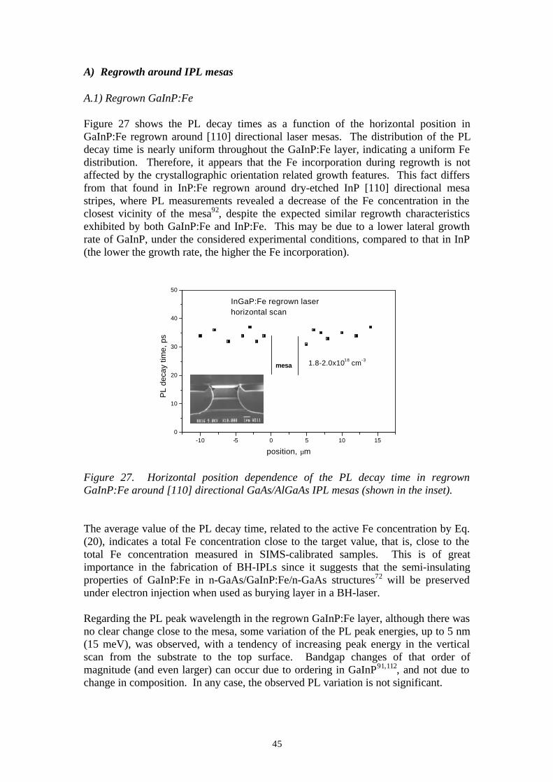
45
A) Regrowth around IPL mesas
A.1) Regrown GaInP:Fe
Figure 27 shows the PL decay times as a function of the horizontal position inGaInP:Fe regrown around [110] directional laser mesas. The distribution of the PLdecay time is nearly uniform throughout the GaInP:Fe layer, indicating a uniform Fedistribution. Therefore, it appears that the Fe incorporation during regrowth is notaffected by the crystallographic orientation related growth features. This fact differsfrom that found in InP:Fe regrown around dry-etched InP [110] directional mesastripes, where PL measurements revealed a decrease of the Fe concentration in theclosest vicinity of the mesa92, despite the expected similar regrowth characteristicsexhibited by both GaInP:Fe and InP:Fe. This may be due to a lower lateral growthrate of GaInP, under the considered experimental conditions, compared to that in InP(the lower the growth rate, the higher the Fe incorporation).
-10 -5 0 5 10 150
10
20
30
40
50
InGaP:Fe regrown laserhorizontal scan
1.8-2.0x1018 cm-3mesa
PL
deca
y tim
e, p
s
position, µm
Figure 27. Horizontal position dependence of the PL decay time in regrownGaInP:Fe around [110] directional GaAs/AlGaAs IPL mesas (shown in the inset).
The average value of the PL decay time, related to the active Fe concentration by Eq.(20), indicates a total Fe concentration close to the target value, that is, close to thetotal Fe concentration measured in SIMS-calibrated samples. This is of greatimportance in the fabrication of BH-IPLs since it suggests that the semi-insulatingproperties of GaInP:Fe in n-GaAs/GaInP:Fe/n-GaAs structures72 will be preservedunder electron injection when used as burying layer in a BH-laser.
Regarding the PL peak wavelength in the regrown GaInP:Fe layer, although there wasno clear change close to the mesa, some variation of the PL peak energies, up to 5 nm(15 meV), was observed, with a tendency of increasing peak energy in the verticalscan from the substrate to the top surface. Bandgap changes of that order ofmagnitude (and even larger) can occur due to ordering in GaInP91,112, and not due tochange in composition. In any case, the observed PL variation is not significant.
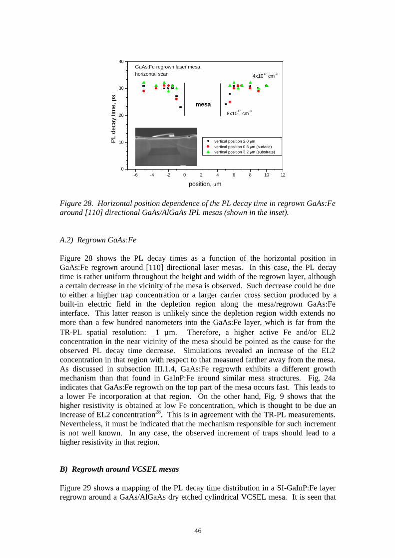
46
-6 -4 -2 0 2 4 6 8 10 120
10
20
30
40
4x1017 cm-3
8x10¹⁷
cm-3
mesa
GaAs:Fe regrown laser mesa horizontal scan
vertical position 2.0 µm vertical position 0.8 µm (surface) vertical position 3.2 µm (substrate)
PL
deca
y tim
e, p
s
position, µm
Figure 28. Horizontal position dependence of the PL decay time in regrown GaAs:Fearound [110] directional GaAs/AlGaAs IPL mesas (shown in the inset).
A.2) Regrown GaAs:Fe
Figure 28 shows the PL decay times as a function of the horizontal position inGaAs:Fe regrown around [110] directional laser mesas. In this case, the PL decaytime is rather uniform throughout the height and width of the regrown layer, althougha certain decrease in the vicinity of the mesa is observed. Such decrease could be dueto either a higher trap concentration or a larger carrier cross section produced by abuilt-in electric field in the depletion region along the mesa/regrown GaAs:Feinterface. This latter reason is unlikely since the depletion region width extends nomore than a few hundred nanometers into the GaAs:Fe layer, which is far from theTR-PL spatial resolution: ∼1 µm. Therefore, a higher active Fe and/or EL2concentration in the near vicinity of the mesa should be pointed as the cause for theobserved PL decay time decrease. Simulations revealed an increase of the EL2concentration in that region with respect to that measured farther away from the mesa.As discussed in subsection III.1.4, GaAs:Fe regrowth exhibits a different growthmechanism than that found in GaInP:Fe around similar mesa structures. Fig. 24aindicates that GaAs:Fe regrowth on the top part of the mesa occurs fast. This leads toa lower Fe incorporation at that region. On the other hand, Fig. 9 shows that thehigher resistivity is obtained at low Fe concentration, which is thought to be due anincrease of EL2 concentration28. This is in agreement with the TR-PL measurements.Nevertheless, it must be indicated that the mechanism responsible for such incrementis not well known. In any case, the observed increment of traps should lead to ahigher resistivity in that region.
B) Regrowth around VCSEL mesas
Figure 29 shows a mapping of the PL decay time distribution in a SI-GaInP:Fe layerregrown around a GaAs/AlGaAs dry etched cylindrical VCSEL mesa. It is seen that
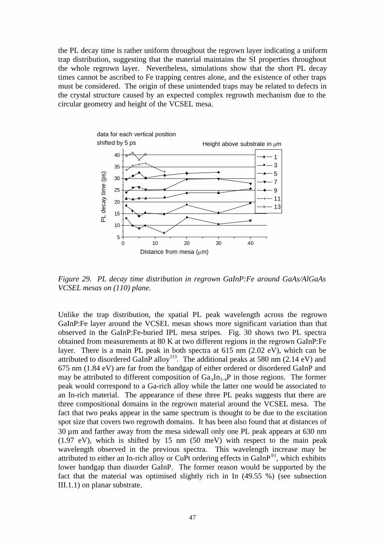
47
the PL decay time is rather uniform throughout the regrown layer indicating a uniformtrap distribution, suggesting that the material maintains the SI properties throughoutthe whole regrown layer. Nevertheless, simulations show that the short PL decaytimes cannot be ascribed to Fe trapping centres alone, and the existence of other trapsmust be considered. The origin of these unintended traps may be related to defects inthe crystal structure caused by an expected complex regrowth mechanism due to thecircular geometry and height of the VCSEL mesa.
Figure 29. PL decay time distribution in regrown GaInP:Fe around GaAs/AlGaAsVCSEL mesas on (110) plane.
Unlike the trap distribution, the spatial PL peak wavelength across the regrownGaInP:Fe layer around the VCSEL mesas shows more significant variation than thatobserved in the GaInP:Fe-buried IPL mesa stripes. Fig. 30 shows two PL spectraobtained from measurements at 80 K at two different regions in the regrown GaInP:Felayer. There is a main PL peak in both spectra at 615 nm (2.02 eV), which can beattributed to disordered GaInP alloy113. The additional peaks at 580 nm (2.14 eV) and675 nm (1.84 eV) are far from the bandgap of either ordered or disordered GaInP andmay be attributed to different composition of GaxIn1-xP in those regions. The formerpeak would correspond to a Ga-rich alloy while the latter one would be associated toan In-rich material. The appearance of these three PL peaks suggests that there arethree compositional domains in the regrown material around the VCSEL mesa. Thefact that two peaks appear in the same spectrum is thought to be due to the excitationspot size that covers two regrowth domains. It has been also found that at distances of30 µm and farther away from the mesa sidewall only one PL peak appears at 630 nm(1.97 eV), which is shifted by 15 nm (50 meV) with respect to the main peakwavelength observed in the previous spectra. This wavelength increase may beattributed to either an In-rich alloy or CuPt ordering effects in GaInP91, which exhibitslower bandgap than disorder GaInP. The former reason would be supported by thefact that the material was optimised slightly rich in In (49.55 %) (see subsectionIII.1.1) on planar substrate.
0 10 20 30 405
10
15
20
25
30
35
40
Height above substrate in µm
data for each vertical positionshifted by 5 ps
1 3 5 7 9 11 13
PL
deca
y tim
e (p
s)
Distance from mesa (µm)
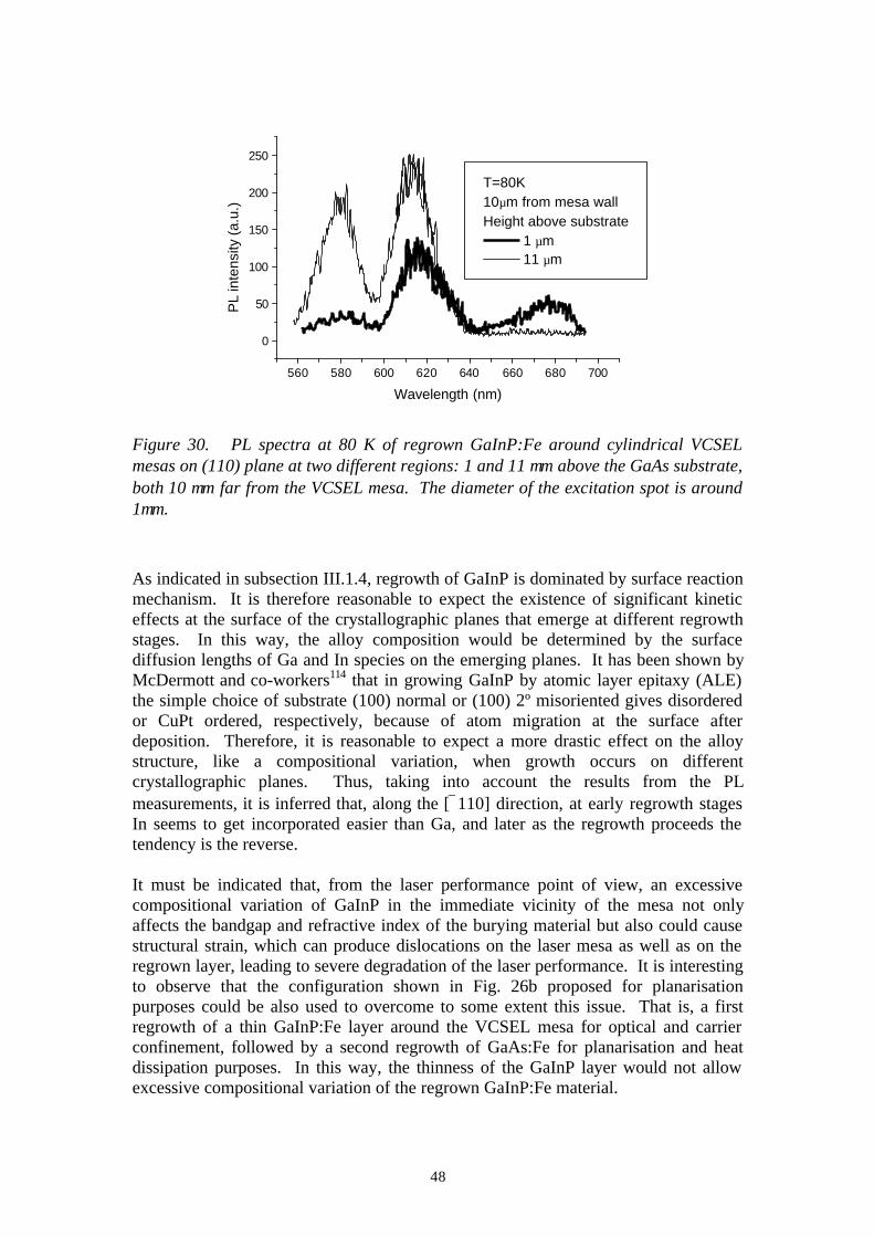
48
Figure 30. PL spectra at 80 K of regrown GaInP:Fe around cylindrical VCSELmesas on (110) plane at two different regions: 1 and 11 µm above the GaAs substrate,both 10 µm far from the VCSEL mesa. The diameter of the excitation spot is around1µm.
As indicated in subsection III.1.4, regrowth of GaInP is dominated by surface reactionmechanism. It is therefore reasonable to expect the existence of significant kineticeffects at the surface of the crystallographic planes that emerge at different regrowthstages. In this way, the alloy composition would be determined by the surfacediffusion lengths of Ga and In species on the emerging planes. It has been shown byMcDermott and co-workers114 that in growing GaInP by atomic layer epitaxy (ALE)the simple choice of substrate (100) normal or (100) 2º misoriented gives disorderedor CuPt ordered, respectively, because of atom migration at the surface afterdeposition. Therefore, it is reasonable to expect a more drastic effect on the alloystructure, like a compositional variation, when growth occurs on differentcrystallographic planes. Thus, taking into account the results from the PLmeasurements, it is inferred that, along the [110] direction, at early regrowth stagesIn seems to get incorporated easier than Ga, and later as the regrowth proceeds thetendency is the reverse.
It must be indicated that, from the laser performance point of view, an excessivecompositional variation of GaInP in the immediate vicinity of the mesa not onlyaffects the bandgap and refractive index of the burying material but also could causestructural strain, which can produce dislocations on the laser mesa as well as on theregrown layer, leading to severe degradation of the laser performance. It is interestingto observe that the configuration shown in Fig. 26b proposed for planarisationpurposes could be also used to overcome to some extent this issue. That is, a firstregrowth of a thin GaInP:Fe layer around the VCSEL mesa for optical and carrierconfinement, followed by a second regrowth of GaAs:Fe for planarisation and heatdissipation purposes. In this way, the thinness of the GaInP layer would not allowexcessive compositional variation of the regrown GaInP:Fe material.
560 580 600 620 640 660 680 700
0
50
100
150
200
250
T=80K10µm from mesa wallHeight above substrate
1 µm 11 µm
PL
inte
nsity
(a.u
.)
Wavelength (nm)
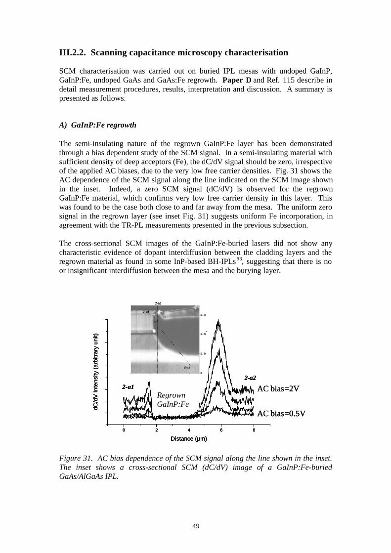
49
III.2.2. Scanning capacitance microscopy characterisation
SCM characterisation was carried out on buried IPL mesas with undoped GaInP,GaInP:Fe, undoped GaAs and GaAs:Fe regrowth. Paper D and Ref. 115 describe indetail measurement procedures, results, interpretation and discussion. A summary ispresented as follows.
A) GaInP:Fe regrowth
The semi-insulating nature of the regrown GaInP:Fe layer has been demonstratedthrough a bias dependent study of the SCM signal. In a semi-insulating material withsufficient density of deep acceptors (Fe), the dC/dV signal should be zero, irrespectiveof the applied AC biases, due to the very low free carrier densities. Fig. 31 shows theAC dependence of the SCM signal along the line indicated on the SCM image shownin the inset. Indeed, a zero SCM signal (dC/dV) is observed for the regrownGaInP:Fe material, which confirms very low free carrier density in this layer. Thiswas found to be the case both close to and far away from the mesa. The uniform zerosignal in the regrown layer (see inset Fig. 31) suggests uniform Fe incorporation, inagreement with the TR-PL measurements presented in the previous subsection.
The cross-sectional SCM images of the GaInP:Fe-buried lasers did not show anycharacteristic evidence of dopant interdiffusion between the cladding layers and theregrown material as found in some InP-based BH-IPLs93, suggesting that there is noor insignificant interdiffusion between the mesa and the burying layer.
Figure 31. AC bias dependence of the SCM signal along the line shown in the inset.The inset shows a cross-sectional SCM (dC/dV) image of a GaInP:Fe-buriedGaAs/AlGaAs IPL.
0 2 4 6 8
dC/d
V In
tens
ity (
arbi
trar
y un
it)
Distance (µm)
2-a22-a1 AC bias=2V
AC bias=0.5V
P1
P2
0 2 4 6 8
dC/d
V In
tens
ity (
arbi
trar
y un
it)
Distance (µm)
2-a22-a1 AC bias=2V
AC bias=0.5V
0 2 4 6 8
dC/d
V In
tens
ity (
arbi
trar
y un
it)
Distance (µm)
2-a22-a1 AC bias=2V
AC bias=0.5V
P1
P2 2-a2
2-b2
2-b1
2-a1
2-a2
2-b2
2-b1
2-a1
RegrownGaInP:Fe
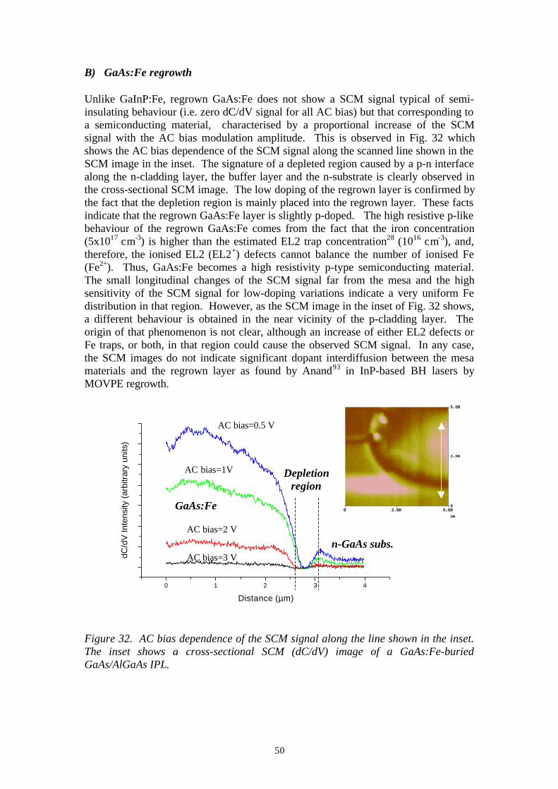
50
B) GaAs:Fe regrowth
Unlike GaInP:Fe, regrown GaAs:Fe does not show a SCM signal typical of semi-insulating behaviour (i.e. zero dC/dV signal for all AC bias) but that corresponding toa semiconducting material, characterised by a proportional increase of the SCMsignal with the AC bias modulation amplitude. This is observed in Fig. 32 whichshows the AC bias dependence of the SCM signal along the scanned line shown in theSCM image in the inset. The signature of a depleted region caused by a p-n interfacealong the n-cladding layer, the buffer layer and the n-substrate is clearly observed inthe cross-sectional SCM image. The low doping of the regrown layer is confirmed bythe fact that the depletion region is mainly placed into the regrown layer. These factsindicate that the regrown GaAs:Fe layer is slightly p-doped. The high resistive p-likebehaviour of the regrown GaAs:Fe comes from the fact that the iron concentration(5x1017 cm-3) is higher than the estimated EL2 trap concentration28 (1016 cm-3), and,therefore, the ionised EL2 (EL2+) defects cannot balance the number of ionised Fe(Fe2+). Thus, GaAs:Fe becomes a high resistivity p-type semiconducting material.The small longitudinal changes of the SCM signal far from the mesa and the highsensitivity of the SCM signal for low-doping variations indicate a very uniform Fedistribution in that region. However, as the SCM image in the inset of Fig. 32 shows,a different behaviour is obtained in the near vicinity of the p-cladding layer. Theorigin of that phenomenon is not clear, although an increase of either EL2 defects orFe traps, or both, in that region could cause the observed SCM signal. In any case,the SCM images do not indicate significant dopant interdiffusion between the mesamaterials and the regrown layer as found by Anand93 in InP-based BH lasers byMOVPE regrowth.
Figure 32. AC bias dependence of the SCM signal along the line shown in the inset.The inset shows a cross-sectional SCM (dC/dV) image of a GaAs:Fe-buriedGaAs/AlGaAs IPL.
0 1 2 3 4
AC bias=0.5V AC bias=1V AC bias=2V AC bias=3V
dC/d
V In
tens
ity (
arbi
trar
y un
its)
Distance (µm)
AC bias=0.5 V
AC bias=1V
AC bias=2 V
AC bias=3 V
GaAs:Fe
n-GaAs subs.
Depletionregion
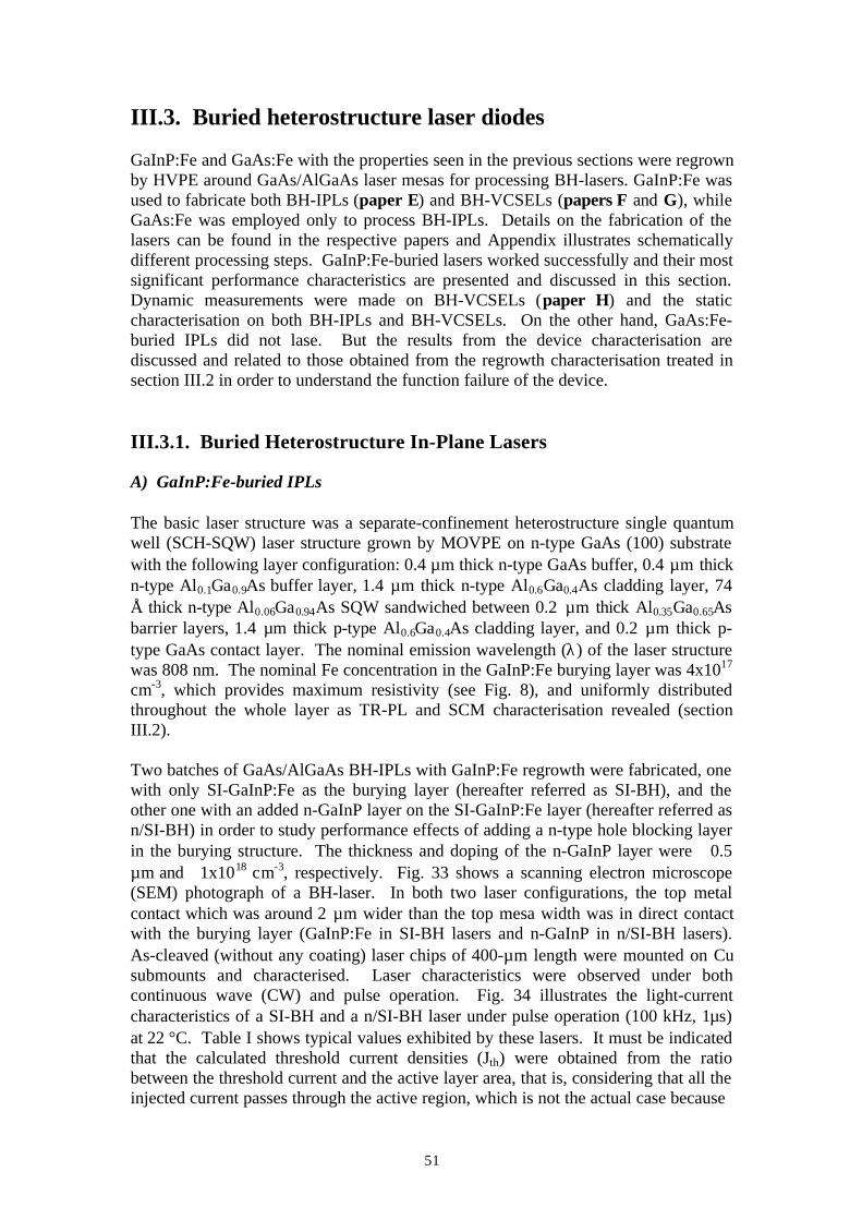
51
III.3. Buried heterostructure laser diodes
GaInP:Fe and GaAs:Fe with the properties seen in the previous sections were regrownby HVPE around GaAs/AlGaAs laser mesas for processing BH-lasers. GaInP:Fe wasused to fabricate both BH-IPLs (paper E) and BH-VCSELs (papers F and G), whileGaAs:Fe was employed only to process BH-IPLs. Details on the fabrication of thelasers can be found in the respective papers and Appendix illustrates schematicallydifferent processing steps. GaInP:Fe-buried lasers worked successfully and their mostsignificant performance characteristics are presented and discussed in this section.Dynamic measurements were made on BH-VCSELs (paper H) and the staticcharacterisation on both BH-IPLs and BH-VCSELs. On the other hand, GaAs:Fe-buried IPLs did not lase. But the results from the device characterisation arediscussed and related to those obtained from the regrowth characterisation treated insection III.2 in order to understand the function failure of the device.
III.3.1. Buried Heterostructure In-Plane Lasers
A) GaInP:Fe-buried IPLs
The basic laser structure was a separate-confinement heterostructure single quantumwell (SCH-SQW) laser structure grown by MOVPE on n-type GaAs (100) substratewith the following layer configuration: 0.4 µm thick n-type GaAs buffer, 0.4 µm thickn-type Al0.1Ga0.9As buffer layer, 1.4 µm thick n-type Al0.6Ga0.4As cladding layer, 74Å thick n-type Al0.06Ga0.94As SQW sandwiched between 0.2 µm thick Al0.35Ga0.65Asbarrier layers, 1.4 µm thick p-type Al0.6Ga0.4As cladding layer, and 0.2 µm thick p-type GaAs contact layer. The nominal emission wavelength (λ) of the laser structurewas 808 nm. The nominal Fe concentration in the GaInP:Fe burying layer was 4x10¹⁷
cm-3, which provides maximum resistivity (see Fig. 8), and uniformly distributedthroughout the whole layer as TR-PL and SCM characterisation revealed (sectionIII.2).
Two batches of GaAs/AlGaAs BH-IPLs with GaInP:Fe regrowth were fabricated, onewith only SI-GaInP:Fe as the burying layer (hereafter referred as SI-BH), and theother one with an added n-GaInP layer on the SI-GaInP:Fe layer (hereafter referred asn/SI-BH) in order to study performance effects of adding a n-type hole blocking layerin the burying structure. The thickness and doping of the n-GaInP layer were ∼0.5µm and ∼1x1018 cm-3, respectively. Fig. 33 shows a scanning electron microscope(SEM) photograph of a BH-laser. In both two laser configurations, the top metalcontact which was around 2 µm wider than the top mesa width was in direct contactwith the burying layer (GaInP:Fe in SI-BH lasers and n-GaInP in n/SI-BH lasers).As-cleaved (without any coating) laser chips of 400-µm length were mounted on Cusubmounts and characterised. Laser characteristics were observed under bothcontinuous wave (CW) and pulse operation. Fig. 34 illustrates the light-currentcharacteristics of a SI-BH and a n/SI-BH laser under pulse operation (100 kHz, 1µs)at 22 °C. Table I shows typical values exhibited by these lasers. It must be indicatedthat the calculated threshold current densities (Jth) were obtained from the ratiobetween the threshold current and the active layer area, that is, considering that all theinjected current passes through the active region, which is not the actual case because
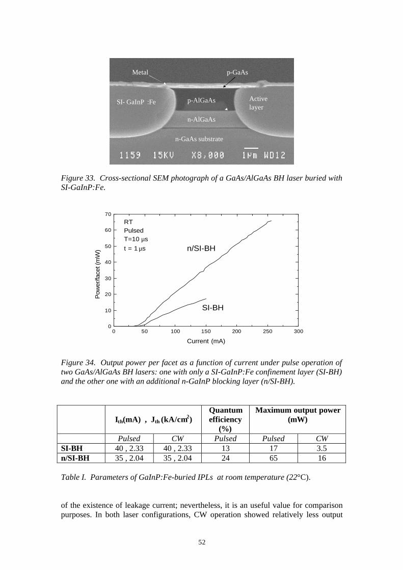
52
Figure 33. Cross-sectional SEM photograph of a GaAs/AlGaAs BH laser buried withSI-GaInP:Fe.
Figure 34. Output power per facet as a function of current under pulse operation oftwo GaAs/AlGaAs BH lasers: one with only a SI-GaInP:Fe confinement layer (SI-BH)and the other one with an additional n-GaInP blocking layer (n/SI-BH).
Ith(mA) , Jth (kA/cm2)Quantumefficiency
(%)
Maximum output power(mW)
Pulsed CW Pulsed Pulsed CWSI-BH 40 , 2.33 40 , 2.33 13 17 3.5n/SI-BH 35 , 2.04 35 , 2.04 24 65 16
Table I. Parameters of GaInP:Fe-buried IPLs at room temperature (22°C).
of the existence of leakage current; nevertheless, it is an useful value for comparisonpurposes. In both laser configurations, CW operation showed relatively less output
SI- GaInP :Fe
n-GaAs substrate
n-AlGaAs
p-AlGaAs Activelayer
Metal p-GaAs
0 50 100 150 200 250 3000
10
20
30
40
50
60
70
RTPulsedT=10 µst = 1 µs n/SI-BH
Pow
er/fa
cet (
mW
)
Current (mA)
SI-BH
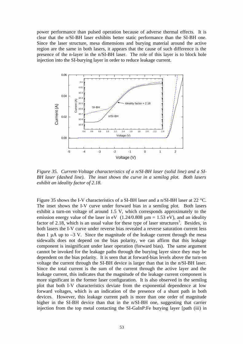
53
power performance than pulsed operation because of adverse thermal effects. It isclear that the n/SI-BH laser exhibits better static performance than the SI-BH one.Since the laser structure, mesa dimensions and burying material around the activeregion are the same in both lasers, it appears that the cause of such difference is thepresence of the n-layer in the n/SI-BH laser. The role of this layer is to block holeinjection into the SI-burying layer in order to reduce leakage current.
Figure 35. Current-Voltage characteristics of a n/SI-BH laser (solid line) and a SI-BH laser (dashed line). The inset shows the curve in a semilog plot. Both lasersexhibit an ideality factor of 2.18.
Figure 35 shows the I-V characteristics of a SI-BH laser and a n/SI-BH laser at 22 °C.The inset shows the I-V curve under forward bias in a semilog plot. Both lasersexhibit a turn-on voltage of around 1.5 V, which corresponds approximately to theemission energy value of the laser in eV (1.24/0.808 µm = 1.53 eV), and an idealityfactor of 2.18, which is an usual value for these type of laser structures3. Besides, inboth lasers the I-V curve under reverse bias revealed a reverse saturation current lessthan 1 µA up to –3 V. Since the magnitude of the leakage current through the mesasidewalls does not depend on the bias polarity, we can affirm that this leakagecomponent is insignificant under laser operation (forward bias). The same argumentcannot be invoked for the leakage paths through the burying layer since they may bedependent on the bias polarity. It is seen that at forward-bias levels above the turn-onvoltage the current through the SI-BH device is larger than that in the n/SI-BH laser.Since the total current is the sum of the current through the active layer and theleakage current, this indicates that the magnitude of the leakage current component ismore significant in the former laser configuration. It is also observed in the semilogplot that both I-V characteristics deviate from the exponential dependence at lowforward voltages, which is an indication of the presence of a shunt path in bothdevices. However, this leakage current path is more than one order of magnitudehigher in the SI-BH device than that in the n/SI-BH one, suggesting that carrierinjection from the top metal contacting the SI-GaInP:Fe burying layer [path (iii) in
-5 -4 -3 -2 -1 0 1 2
0.00
0.02
0.04
0.06
Cur
rren
t (A
)
Voltage (V)
0.4 0.6 0.8 1.0 1.2 1.4 1.6 1.8 2.0 2.2 2.4
1E-9
1E-8
1E-7
1E-6
1E-5
1E-4
1E-3
0.01
0.1
n/SI-BH
SI-BHIdeality factor = 2.18
Cur
rent
(A)
Voltage (V)
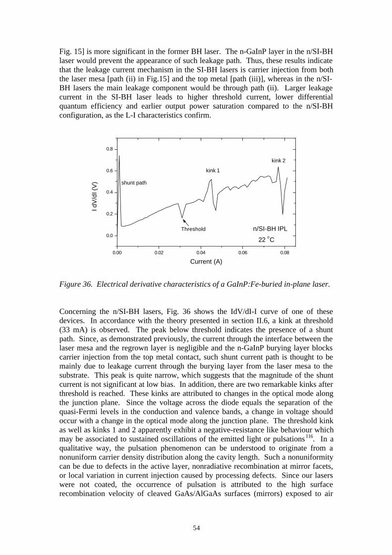
54
Fig. 15] is more significant in the former BH laser. The n-GaInP layer in the n/SI-BHlaser would prevent the appearance of such leakage path. Thus, these results indicatethat the leakage current mechanism in the SI-BH lasers is carrier injection from boththe laser mesa [path (ii) in Fig.15] and the top metal [path (iii)], whereas in the n/SI-BH lasers the main leakage component would be through path (ii). Larger leakagecurrent in the SI-BH laser leads to higher threshold current, lower differentialquantum efficiency and earlier output power saturation compared to the n/SI-BHconfiguration, as the L-I characteristics confirm.
Figure 36. Electrical derivative characteristics of a GaInP:Fe-buried in-plane laser.
Concerning the n/SI-BH lasers, Fig. 36 shows the IdV/dI-I curve of one of thesedevices. In accordance with the theory presented in section II.6, a kink at threshold(33 mA) is observed. The peak below threshold indicates the presence of a shuntpath. Since, as demonstrated previously, the current through the interface between thelaser mesa and the regrown layer is negligible and the n-GaInP burying layer blockscarrier injection from the top metal contact, such shunt current path is thought to bemainly due to leakage current through the burying layer from the laser mesa to thesubstrate. This peak is quite narrow, which suggests that the magnitude of the shuntcurrent is not significant at low bias. In addition, there are two remarkable kinks afterthreshold is reached. These kinks are attributed to changes in the optical mode alongthe junction plane. Since the voltage across the diode equals the separation of thequasi-Fermi levels in the conduction and valence bands, a change in voltage shouldoccur with a change in the optical mode along the junction plane. The threshold kinkas well as kinks 1 and 2 apparently exhibit a negative-resistance like behaviour whichmay be associated to sustained oscillations of the emitted light or pulsations 116. In aqualitative way, the pulsation phenomenon can be understood to originate from anonuniform carrier density distribution along the cavity length. Such a nonuniformitycan be due to defects in the active layer, nonradiative recombination at mirror facets,or local variation in current injection caused by processing defects. Since our laserswere not coated, the occurrence of pulsation is attributed to the high surfacerecombination velocity of cleaved GaAs/AlGaAs surfaces (mirrors) exposed to air
0.00 0.02 0.04 0.06 0.08
0.0
0.2
0.4
0.6
0.8
n/SI-BH IPL
22 oC
shunt path
kink 2
kink 1
Threshold
I dV
/dI (
V)
Current (A)
55
(∼107 cm/s)98. This surface recombination can be reduced by coating the cleavedsurfaces. Besides, the above-threshold variation of IdV/dI with I exhibits certainsublinearity and small kinks at high injection current, which can be associated withthe existence of leakage current and changes in the optical field distribution,respectively94.
The refractive index at λ = 808 nm of the Ga0.51In0.49P burying layer and theAl0.6Ga0.4As cladding layers is around 3.25 117 and 3.27 118, respectively, whereas forthe Al0.35Ga0.65As barrier layers and active layer it is around 3.4 and 3.63 (From Fig.3), respectively. That is, the active region is surrounded everywhere by lowerrefractive index materials, and therefore optical index guiding confinement shouldhappen. The measured near field intensity distribution of the GaInP:Fe-buried IPL(n/SI-BH) showed single lateral mode operation up to ∼5 mW CW output power.Inoue and co-workers11 reported fundamental spatial mode operation up to 35 mWCW output power for an AlGaAs BH-laser diode (λ = 808 nm) fabricated entirely byMOVPE, with an active region width of 4.3 µm surrounded by Al0.35Ga0.65As opticalguiding layers and high resistivity Al0.5Ga0.5As burying layer. The high single modeoperation output power demonstrated by the aforementioned authors is probably dueto the use of high reflectivity facet coating. In these lasers, the higher bandgap (1.93eV) and lower refractive index of Al 0.5Ga0.5As compared to Ga0.51In0.49P (1.9 eV)would lead to the appearance of higher order lateral modes at lower output powerbecause of an expected stronger index guiding mechanism (higher refractive indexstep between the active and the burying layer). Proper facet coating can enhance thedifferential quantum efficiency and reduces the threshold current of a Fabry-Perotedge-emitting laser3.
In a rigorous way, in order to compare the performance of SI-GaInP-buried (n/SI-BH)lasers with that exhibited by SI-AlGaAs or reversed p-n AlGaAs-buried IPLs, deviceswith the same laser structure and mesa dimensions but with AlGaAs burying layershould be fabricated and characterised. However, selective regrowth of a thickAlGaAs layer should be achieved by an epitaxial technique other than HVPE becauseof its limitation in growing Al-containing materials. Nevertheless, other epitaxialtechniques such as MOVPE and MBE do not present the same flexibility as HVPE forthis purpose, making the regrowth of such thick layer very difficult. In any case, ourresults can be compared with those from similar structures reported by other authorsin order to have a comparative estimation. For example, Hong et al.10 fabricatedAlGaAs BH lasers (λ = 881 nm) by wet etching and SI-Al0.5Ga0.5As regrowth byMOVPE, with a threshold current density of 2.1 kA/cm2 under CW operation and adifferential quantum efficiency of 40% per facet (coated). Welch et al.119 reported athreshold current density of 5.3 kA/cm2 under both CW and pulsed operation and adifferential quantum efficiency of 40% per facet (coated) for a AlGaAs BH laser (λ =825 nm) using an AlGaAs forward bias junction current confining layer grown byMOVPE. The differential quantum efficiency reported by these authors is higher thanthat exhibited by SI-GaInP buried lasers, which is probably because of the coating ofthe facets. On the other hand, the threshold current density of the SI-GaInP buriedIPLs (2.04 kA/cm2) is comparable to those reported by the aforementioned authors. Itmust be indicated that the obtained results are quite similar to those reported byLourdudoss et al.26 in Al-free GaInP/GaInAsP/GaAs (λ = 905 nm) BH-IPLs with SI-GaInP burying layer (Jth = 2.0 kA/cm2, slope efficiency = 0.37 W/A and maximumoutput power = 14 mW under RT-CW operation).
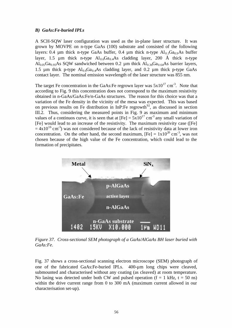
56
B) GaAs:Fe-buried IPLs
A SCH-SQW laser configuration was used as the in-plane laser structure. It wasgrown by MOVPE on n-type GaAs (100) substrate and consisted of the followinglayers: 0.4 µm thick n-type GaAs buffer, 0.4 µm thick n-type Al0.1Ga0.9As bufferlayer, 1.5 µm thick n-type Al0.6Ga0.4As cladding layer, 200 Å thick n-typeAl0.05Ga0.95As SQW sandwiched between 0.2 µm thick Al0.36Ga0.64As barrier layers,1.5 µm thick p-type Al0.6Ga0.4As cladding layer, and 0.2 µm thick p-type GaAscontact layer. The nominal emission wavelength of the laser structure was 855 nm.
The target Fe concentration in the GaAs:Fe regrown layer was 5x1017 cm-3. Note thataccording to Fig. 9 this concentration does not correspond to the maximum resistivityobtained in n-GaAs/GaAs:Fe/n-GaAs structures. The reason for this choice was that avariation of the Fe density in the vicinity of the mesa was expected. This was basedon previous results on Fe distribution in InP:Fe regrowth92, as discussed in sectionIII.2. Thus, considering the measured points in Fig. 9 as maximum and minimumvalues of a continuos curve, it is seen that at [Fe] = 5x1017 cm-3 any small variation of[Fe] would lead to an increase of the resistivity. The maximum resistivity case ([Fe]= 4x1016 cm-3) was not considered because of the lack of resistivity data at lower ironconcentration. On the other hand, the second maximum, [Fe] = 1x1020 cm-3, was notchosen because of the high value of the Fe concentration, which could lead to theformation of precipitates.
Figure 37. Cross-sectional SEM photograph of a GaAs/AlGaAs BH laser buried withGaAs:Fe.
Fig. 37 shows a cross-sectional scanning electron microscope (SEM) photograph ofone of the fabricated GaAs:Fe-buried IPLs. 400-µm long chips were cleaved,submounted and characterised without any coating (as cleaved) at room temperature.No lasing was detected under both CW and pulsed operation (f = 1 kHz, t = 50 ns)within the drive current range from 0 to 300 mA (maximum current allowed in ourcharacterisation set-up).
GaAs:Fe
p-AlGaAs
n-AlGaAs
active layer
n-GaAs substrate
Metal SiNx

57
Assuming that the basic laser structure is without any malfunction, the non-lasingcould be due to two major reasons: (1) excessive leakage current and/or (2) very weakoptical confinement (low confinement factor) because of the antiguiding effect causedby the higher refractive index GaAs:Fe burying layer. Both factors can contribute toan increase in the threshold current in a BH-laser95. Yoo et al.29 reported on theperformance of 850-nm wavelength BH-VCSELs with amorphous GaAs as theburying layer. Despite the low optical confinement provided by the high refractiveindex burying material, low threshold currents were obtained and the antiguidingeffect was successfully used in obtaining stable fundamental transverse mode. Sincethe emission wavelength and burying layer refractive index of our devices are similarto those presented by the aforementioned authors, reason (2) may be rejected.
Thus, a high leakage current through the device should be pointed as the main reasonfor the obtained performance. It is observed in Fig. 37 that the top metal contact isextended laterally on the GaAs:Fe regrown layer around 1.5 µm, that is, 1/4 of thetotal width of the top metal contact. This is a common situation in the fabrication ofBH-lasers when the mesa width is very narrow. As indicated in section II.7, this cancreate a leakage path through the burying layer [path (iii) in Fig. 15]. In order tostudy this possible leakage current path, p-metal/GaAs:Fe/n+-GaAs structuresavailable in between the two laser mesas were recovered, see Fig. 38, and subjected toI-V measurements. Fig. 39 shows the I-V characteristics of a GaAs:Fe-buried laserand a p-metal/GaAs:Fe/n+-GaAs structure normalised to the top metal contact widthof 1.5 µm. In all the cases, V is defined as the voltage in the top metal pad minus thevoltage in the bottom contact. The current through the BH-laser under reverse bias isvery small, less than 1 µA up to –5 V. This indicates that the leakage current alongthe interface between the laser mesa and the regrown GaAs:Fe layer is negligible. Inaddition, it is observed that the p-metal/GaAs:Fe/n+-GaAs structure and the BH-laserexhibit different forward breakdown voltage, ∼1 V and ∼1.43 V, respectively. Theformer turn-on voltage can be identified as that corresponding to the GaAs:Fe/n+-GaAs junction. The facts that the n-GaAs substrate is highly doped and the value ofthe turn-on voltage is lower than 1.42 V (GaAs bandgap = 1.42 eV) suggest that theGaAs:Fe material is slightly p-doped. This is in agreement with the SCM resultsobtained in regrown GaAs:Fe far from the laser mesa (subsection III.2.2). On theother hand, the turn-on voltage exhibited by the BH-laser indicates that the currentpath (iii) does not dominate in this device. It is thought that this is caused by the factrevealed by the TR-PL and SCM measurements (section III.2) about the increment ofthe trap concentration in the immediate vicinity of the laser mesa, which wouldincrease the resistivity of the regrown GaAs:Fe in this region, and thereby decreasethe magnitude of leakage path (iii). In this way, the BH laser turn-on voltage mayoriginate from either current through the laser p-n junction or leakage currentbypassing the active layer through the GaAs:Fe burying layer via the cladding layers[path (ii) in Fig. 15]. The turn-on voltage of the laser p-n junction should correspondapproximately to the active layer bandgap in volts, that is, 1.24/0.855 µm = 1.45 V.Nevertheless, the structure defined by path (ii) may also lead to a similar breakdownforward voltage because of the GaAs:Fe bandgap. In order to determine the dominantcurrent path, the ideality factor of the I-V curve of the BH-laser was determined. It isseen in the semilog I-V plot (inset in Fig. 39) that, before the turn-on voltage isreached, the curve follows an exponential growth with an ideality factor of 2.82. Forcommon heterostructure lasers the diode ideality factor is approximately 2 as seen inthe previous subsection for GaInP:Fe-buried IPLs. High values of the ideality factor
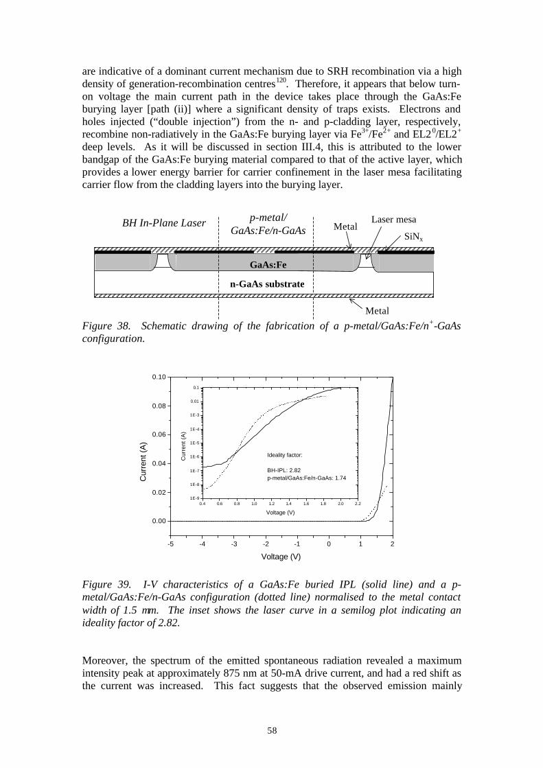
58
are indicative of a dominant current mechanism due to SRH recombination via a highdensity of generation-recombination centres120. Therefore, it appears that below turn-on voltage the main current path in the device takes place through the GaAs:Feburying layer [path (ii)] where a significant density of traps exists. Electrons andholes injected (“double injection”) from the n- and p-cladding layer, respectively,recombine non-radiatively in the GaAs:Fe burying layer via Fe3+/Fe2+ and EL20/EL2+
deep levels. As it will be discussed in section III.4, this is attributed to the lowerbandgap of the GaAs:Fe burying material compared to that of the active layer, whichprovides a lower energy barrier for carrier confinement in the laser mesa facilitatingcarrier flow from the cladding layers into the burying layer.
Figure 38. Schematic drawing of the fabrication of a p-metal/GaAs:Fe/n+-GaAsconfiguration.
Figure 39. I-V characteristics of a GaAs:Fe buried IPL (solid line) and a p-metal/GaAs:Fe/n-GaAs configuration (dotted line) normalised to the metal contactwidth of 1.5 µm. The inset shows the laser curve in a semilog plot indicating anideality factor of 2.82.
Moreover, the spectrum of the emitted spontaneous radiation revealed a maximumintensity peak at approximately 875 nm at 50-mA drive current, and had a red shift asthe current was increased. This fact suggests that the observed emission mainly
n-GaAs substrate
GaAs:Fe
p-metal/GaAs:Fe/n-GaAs
BH In-Plane Laser Metal
Metal
SiNx
Laser mesa
0.4 0.6 0.8 1.0 1.2 1.4 1.6 1.8 2.0 2.21E-9
1E-8
1E-7
1E-6
1E-5
1E-4
1E-3
0.01
0.1
Ideality factor:
BH-IPL: 2.82p-metal/GaAs:Fe/n-GaAs: 1.74
Cur
rent
(A
)
Voltage (V)
-5 -4 -3 -2 -1 0 1 2
0.00
0.02
0.04
0.06
0.08
0.10
Cur
rent
(A)
Voltage (V)
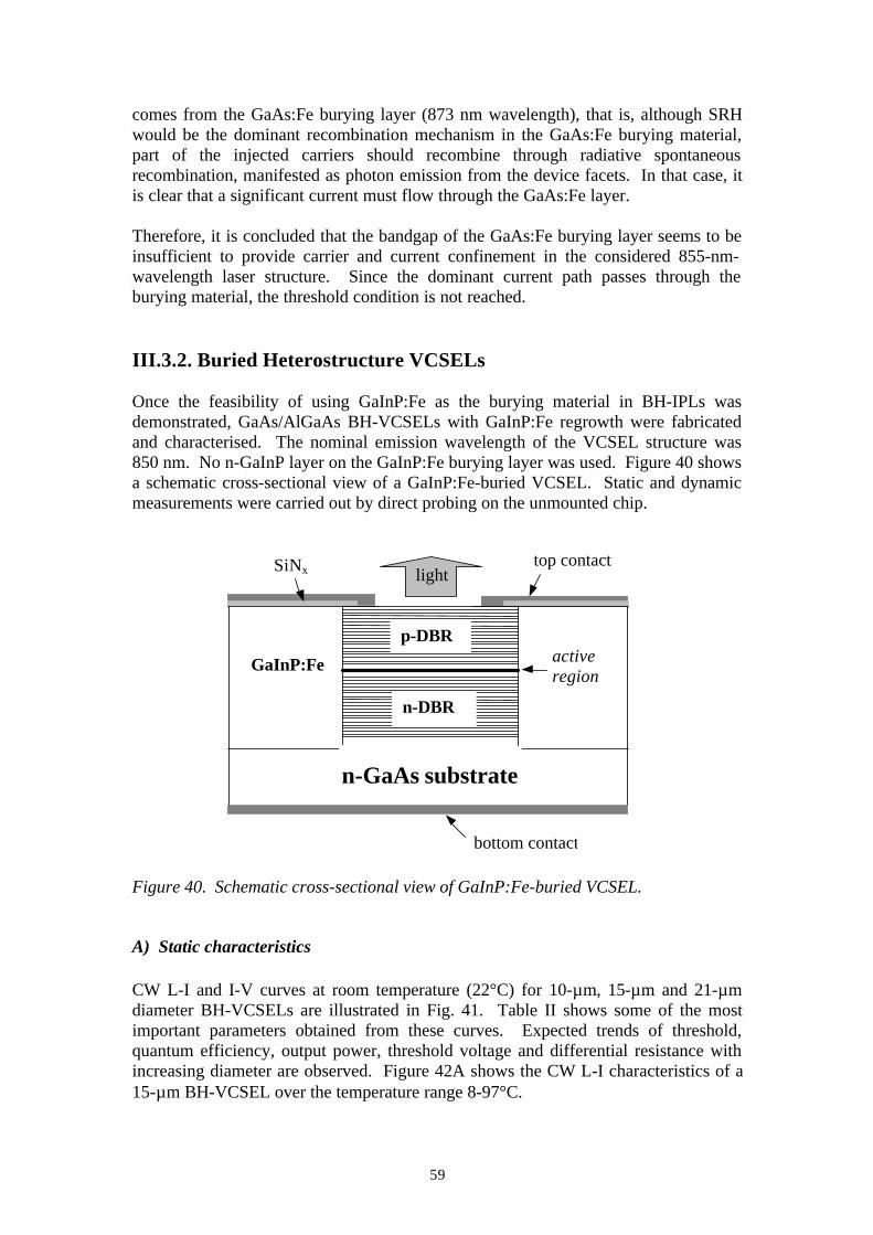
59
comes from the GaAs:Fe burying layer (873 nm wavelength), that is, although SRHwould be the dominant recombination mechanism in the GaAs:Fe burying material,part of the injected carriers should recombine through radiative spontaneousrecombination, manifested as photon emission from the device facets. In that case, itis clear that a significant current must flow through the GaAs:Fe layer.
Therefore, it is concluded that the bandgap of the GaAs:Fe burying layer seems to beinsufficient to provide carrier and current confinement in the considered 855-nm-wavelength laser structure. Since the dominant current path passes through theburying material, the threshold condition is not reached.
III.3.2. Buried Heterostructure VCSELs
Once the feasibility of using GaInP:Fe as the burying material in BH-IPLs wasdemonstrated, GaAs/AlGaAs BH-VCSELs with GaInP:Fe regrowth were fabricatedand characterised. The nominal emission wavelength of the VCSEL structure was850 nm. No n-GaInP layer on the GaInP:Fe burying layer was used. Figure 40 showsa schematic cross-sectional view of a GaInP:Fe-buried VCSEL. Static and dynamicmeasurements were carried out by direct probing on the unmounted chip.
Figure 40. Schematic cross-sectional view of GaInP:Fe-buried VCSEL.
A) Static characteristics
CW L-I and I-V curves at room temperature (22°C) for 10-µm, 15-µm and 21-µmdiameter BH-VCSELs are illustrated in Fig. 41. Table II shows some of the mostimportant parameters obtained from these curves. Expected trends of threshold,quantum efficiency, output power, threshold voltage and differential resistance withincreasing diameter are observed. Figure 42A shows the CW L-I characteristics of a15-µm BH-VCSEL over the temperature range 8-97°C.
GaInP:Fe
n-GaAs substrate
activeregion
p-DBR
n-DBR
top contact light
bottom contact
SiNx
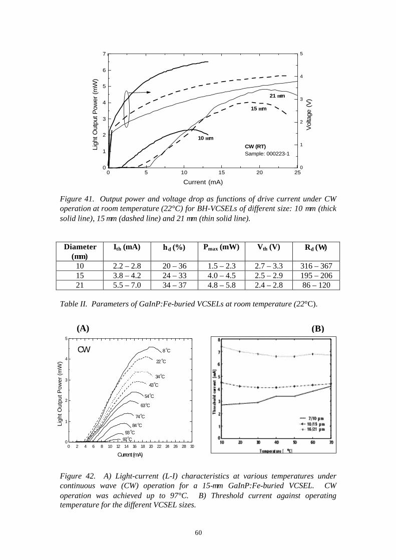
60
Figure 41. Output power and voltage drop as functions of drive current under CWoperation at room temperature (22°C) for BH-VCSELs of different size: 10 µm (thicksolid line), 15 µm (dashed line) and 21 µm (thin solid line).
Diameter(µm)
Ith (mA) ηd (%) Pmax (mW) Vth (V) Rd (Ω)
10 2.2 – 2.8 20 – 36 1.5 – 2.3 2.7 – 3.3 316 – 36715 3.8 – 4.2 24 – 33 4.0 – 4.5 2.5 – 2.9 195 – 20621 5.5 – 7.0 34 – 37 4.8 – 5.8 2.4 – 2.8 86 – 120
Table II. Parameters of GaInP:Fe-buried VCSELs at room temperature (22°C).
Figure 42. A) Light-current (L-I) characteristics at various temperatures undercontinuous wave (CW) operation for a 15-µm GaInP:Fe-buried VCSEL. CWoperation was achieved up to 97°C. B) Threshold current against operatingtemperature for the different VCSEL sizes.
0 5 10 15 20 250
1
2
3
4
5
6
7
10 µm
21 µm
15 µm
CW (RT)Sample: 000223-1
Ligh
t Out
put P
ower
(m
W)
Current (mA)
0
1
2
3
4
5
Vol
tage
(V
)
0 2 4 6 8 10 12 14 16 18 20 22 24 26 28 300
1
2
3
4
5
CW
97 oC93 oC
84 oC
74 oC
63 oC
54 oC
43 oC
34 oC
22 oC
8 oC
Ligh
t Out
put P
ower
(m
W)
Current (mA)
(B)(A)
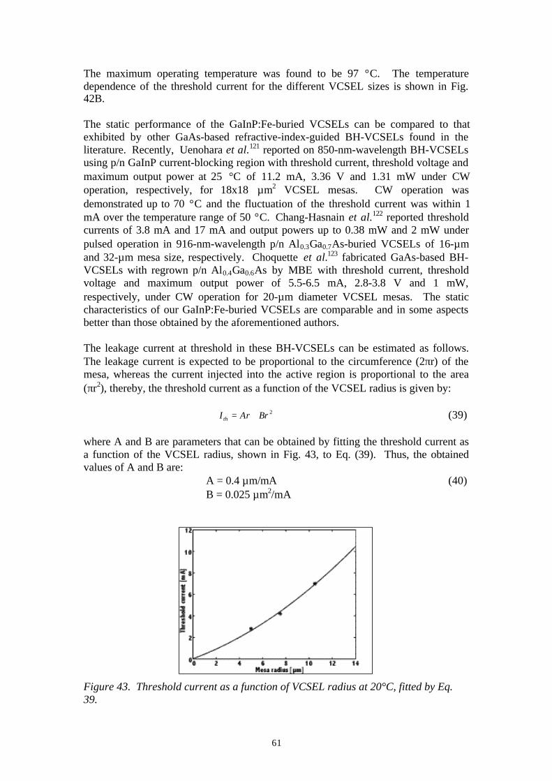
61
The maximum operating temperature was found to be 97 °C. The temperaturedependence of the threshold current for the different VCSEL sizes is shown in Fig.42B.
The static performance of the GaInP:Fe-buried VCSELs can be compared to thatexhibited by other GaAs-based refractive-index-guided BH-VCSELs found in theliterature. Recently, Uenohara et al.121 reported on 850-nm-wavelength BH-VCSELsusing p/n GaInP current-blocking region with threshold current, threshold voltage andmaximum output power at 25 °C of 11.2 mA, 3.36 V and 1.31 mW under CWoperation, respectively, for 18x18 µm2 VCSEL mesas. CW operation wasdemonstrated up to 70 °C and the fluctuation of the threshold current was within 1mA over the temperature range of 50 °C. Chang-Hasnain et al.122 reported thresholdcurrents of 3.8 mA and 17 mA and output powers up to 0.38 mW and 2 mW underpulsed operation in 916-nm-wavelength p/n Al0.3Ga0.7As-buried VCSELs of 16-µmand 32-µm mesa size, respectively. Choquette et al.123 fabricated GaAs-based BH-VCSELs with regrown p/n Al0.4Ga0.6As by MBE with threshold current, thresholdvoltage and maximum output power of 5.5-6.5 mA, 2.8-3.8 V and 1 mW,respectively, under CW operation for 20-µm diameter VCSEL mesas. The staticcharacteristics of our GaInP:Fe-buried VCSELs are comparable and in some aspectsbetter than those obtained by the aforementioned authors.
The leakage current at threshold in these BH-VCSELs can be estimated as follows.The leakage current is expected to be proportional to the circumference (2πr) of themesa, whereas the current injected into the active region is proportional to the area(πr2), thereby, the threshold current as a function of the VCSEL radius is given by:
I Ar Brth = + 2 (39)
where A and B are parameters that can be obtained by fitting the threshold current asa function of the VCSEL radius, shown in Fig. 43, to Eq. (39). Thus, the obtainedvalues of A and B are:
A = 0.4 µm/mA (40) B = 0.025 µm2/mA
Figure 43. Threshold current as a function of VCSEL radius at 20°C, fitted by Eq.39.
62
That is, for the smallest device, the leakage current represents 76% of the totalthreshold current, while the corresponding number is 60% for the largest one. It mustbe noted that these are rough estimations since the threshold current depends on themodal behaviour and the optical losses that also vary with device size. In addition, thefirst term of the sum in Eq. (39), Ar, also includes current due to nonradiativerecombination via surface states on the etched sides of the active region, which isproportional to the circumference of the VCSEL mesa, too.
In order to determine the main leakage current mechanism, I-V characteristics underboth reverse and forward bias were studied. Fig. 44 shows the semilog I-V curve at25 °C for 10-µm, 15-µm and 21-µm size BH-VCSELs. It is observed that the reversecurrent is less than 1 nA up to –5V for all sizes, indicating that the leakage currentthrough the mesa sidewalls [path (i) in Fig. 15] is insignificant. This is an importantresult since it confirms the successful regrowth of the burying material around thewhole mesa sidewall surface and demonstrates the benefits of our epitaxial regrowthtechnique in passivating surface defects on the mesa sidewalls created by an ionbeam-based etching process. Therefore, it can be affirmed that the leakage current inthe GaInP:Fe-buried VCSELs flows through the burying layer. According to theschematic cross-section of the BH-VCSEL shown in Fig. 40, this leakage shouldoccur only because of carrier injection from the VCSEL mesa into the GaInP:Feburying layer [path (ii) in Fig. 15] since the top metal contact does not contact the SI-material. However, the real devices present certain misalignment among the SiNopening, the contact opening and the mesa circumference produced during thephotolithographic process. As a result of such misalignment, part of the top contactlies on the SI-burying layer, leading to a leakage current path through this layer [path(iii) in Fig. 15]. The magnitude of the latter leakage path must be proportional to themetal area contacting the SI-material. This is illustrated in Fig. 45, which shows theI-V characteristics of two 15-µm BH-VCSELs, one with a small contact area on theSI-layer (small misalignment), laser A, and the other one with a larger misalignment(larger contact area on the burying layer), laser B. The laser performance presented inthe previous subsections and the appended papers corresponds to BH-VCSELs typeA. It is seen that laser B exhibits a higher current under reverse bias. In addition, atlow forward bias the I-V curve of laser B deviates from that of laser A (which followsan exponential dependence), showing a kink that indicates the presence of a shuntpath. Since the I-V curve of laser B at low reverse and forward voltage is notsymmetric, the observed shunt path cannot be attributed to leakage through the mesasidewalls. On the other hand, the fact that the kink at low forward voltages is not seenin laser A suggests that the shunt path in laser B is because of the aforementionedlarger metal contact area over the SI-GaInP:Fe material. Since laser A does notexhibit such behaviour, it is concluded that the main leakage path in the GaInP:Fe-buried VCSELs is due to carrier injection from the laser mesa into the burying layer[path (ii)]. Therefore, the previously calculated leakage percentage at thresholdwould correspond to this leakage path.
As mentioned before, if the top metal contacts the burying material an additionalleakage path appears, which may degrade the laser performance. In order to avoidsuch contact and consequent leakage a precise lithography must be achieved. Thisshould be facilitated by a more planar top surface (improved regrowth planarisation).An alternative method to eliminate leakage path (iii) would be to regrow an n-type
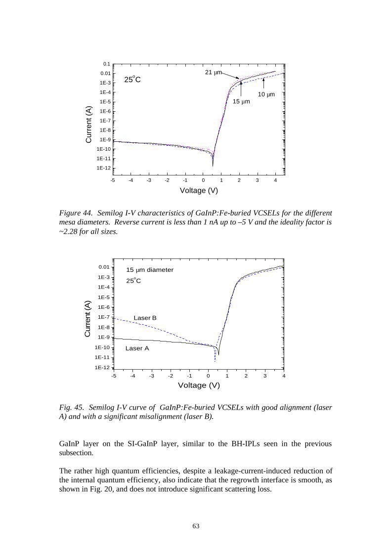
63
Figure 44. Semilog I-V characteristics of GaInP:Fe-buried VCSELs for the differentmesa diameters. Reverse current is less than 1 nA up to –5 V and the ideality factor is∼2.28 for all sizes.
Fig. 45. Semilog I-V curve of GaInP:Fe-buried VCSELs with good alignment (laserA) and with a significant misalignment (laser B).
GaInP layer on the SI-GaInP layer, similar to the BH-IPLs seen in the previoussubsection.
The rather high quantum efficiencies, despite a leakage-current-induced reduction ofthe internal quantum efficiency, also indicate that the regrowth interface is smooth, asshown in Fig. 20, and does not introduce significant scattering loss.
-5 -4 -3 -2 -1 0 1 2 3 4
1E-12
1E-11
1E-10
1E-9
1E-8
1E-7
1E-6
1E-5
1E-4
1E-3
0.01
0.1
25oC21 µm
15 µm10 µm
Cur
rent
(A)
Voltage (V)
-5 -4 -3 -2 -1 0 1 2 3 4
1E-12
1E-11
1E-10
1E-9
1E-8
1E-7
1E-6
1E-5
1E-4
1E-3
0.01
Laser B
Laser A
15 µm diameter
25oC
Cur
rent
(A)
Voltage (V)
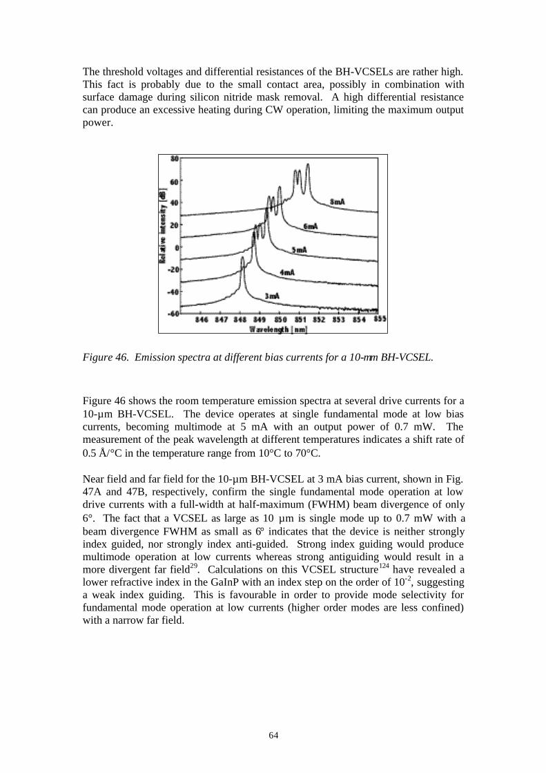
64
The threshold voltages and differential resistances of the BH-VCSELs are rather high.This fact is probably due to the small contact area, possibly in combination withsurface damage during silicon nitride mask removal. A high differential resistancecan produce an excessive heating during CW operation, limiting the maximum outputpower.
Figure 46. Emission spectra at different bias currents for a 10-µm BH-VCSEL.
Figure 46 shows the room temperature emission spectra at several drive currents for a10-µm BH-VCSEL. The device operates at single fundamental mode at low biascurrents, becoming multimode at 5 mA with an output power of 0.7 mW. Themeasurement of the peak wavelength at different temperatures indicates a shift rate of0.5 Å/°C in the temperature range from 10°C to 70°C.
Near field and far field for the 10-µm BH-VCSEL at 3 mA bias current, shown in Fig.47A and 47B, respectively, confirm the single fundamental mode operation at lowdrive currents with a full-width at half-maximum (FWHM) beam divergence of only6°. The fact that a VCSEL as large as 10 µm is single mode up to 0.7 mW with abeam divergence FWHM as small as 6° indicates that the device is neither stronglyindex guided, nor strongly index anti-guided. Strong index guiding would producemultimode operation at low currents whereas strong antiguiding would result in amore divergent far field29. Calculations on this VCSEL structure124 have revealed alower refractive index in the GaInP with an index step on the order of 10-2, suggestinga weak index guiding. This is favourable in order to provide mode selectivity forfundamental mode operation at low currents (higher order modes are less confined)with a narrow far field.
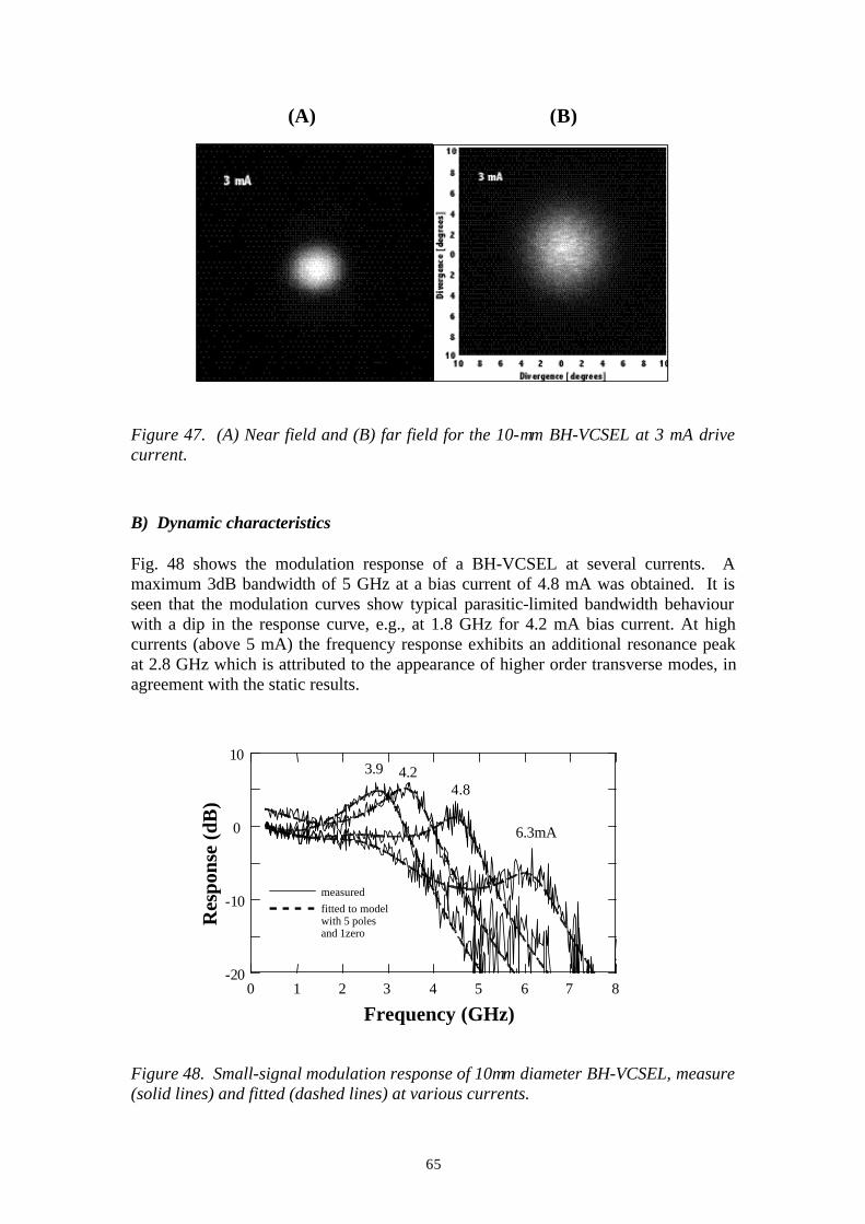
65
(A) (B)
Figure 47. (A) Near field and (B) far field for the 10-µm BH-VCSEL at 3 mA drivecurrent.
B) Dynamic characteristics
Fig. 48 shows the modulation response of a BH-VCSEL at several currents. Amaximum 3dB bandwidth of 5 GHz at a bias current of 4.8 mA was obtained. It isseen that the modulation curves show typical parasitic-limited bandwidth behaviourwith a dip in the response curve, e.g., at 1.8 GHz for 4.2 mA bias current. At highcurrents (above 5 mA) the frequency response exhibits an additional resonance peakat 2.8 GHz which is attributed to the appearance of higher order transverse modes, inagreement with the static results.
measuredfitted to modelwith 5 polesand 1zero
0 1 2 3 4 5 6 7 8-20
-10
0
10
Frequency (GHz)
Res
pons
e (d
B)
3.9 4.24.8
6.3mA
Figure 48. Small-signal modulation response of 10µm diameter BH-VCSEL, measure(solid lines) and fitted (dashed lines) at various currents.
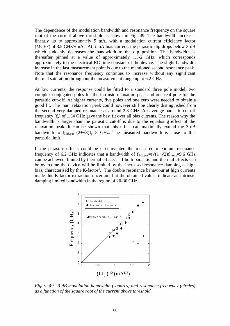
66
The dependence of the modulation bandwidth and resonance frequency on the squareroot of the current above threshold is shown in Fig. 49. The bandwidth increaseslinearly up to approximately 5 mA, with a modulation current efficiency factor(MCEF) of 3.5 GHz/√mA. At 5 mA bias current, the parasitic dip drops below 3-dBwhich suddenly decreases the bandwidth to the dip position. The bandwidth isthereafter pinned at a value of approximately 1.5-2 GHz, which correspondsapproximately to the electrical RC time constant of the device. The slight bandwidthincrease in the last measurement point is due to the mentioned second resonance peak.Note that the resonance frequency continues to increase without any significantthermal saturation throughout the measurement range up to 6.2 GHz.
At low currents, the response could be fitted to a standard three pole model; twocomplex-conjugated poles for the intrinsic relaxation peak and one real pole for theparasitic cut-off. At higher currents, five poles and one zero were needed to obtain agood fit. The main relaxation peak could however still be clearly distinguished fromthe second very damped resonance at around 2.8 GHz. An average parasitic cut-offfrequency (fp) of 1.34 GHz gave the best fit over all bias currents. The reason why thebandwidth is larger than the parasitic cutoff is due to the equalising effect of therelaxation peak. It can be shown that this effect can maximally extend the 3-dBbandwidth to f3dB,par=(2+√3)fp=5 GHz. The measured bandwidth is close to thisparasitic limit.
If the parasitic effects could be circumvented the measured maximum resonancefrequency of 6.2 GHz indicates that a bandwidth of f3dB,par=(√(1+√2)fr,max=9.6 GHzcan be achieved, limited by thermal effects3. If both parasitic and thermal effects canbe overcome the device will be limited by the increased resonance damping at highbias, characterised by the K-factor3. The double resonance behaviour at high currentsmade this K-factor extraction uncertain, but the obtained values indicate an intrinsicdamping limited bandwidth in the region of 20-30 GHz.
Figure 49. 3-dB modulation bandwidth (squares) and resonance frequency (circles)as a function of the square root of the current above threshold.
Re so nan ce fr e que ncy
Ba n dw idt h
0
1
2
3
4
5
6
7
0 0.5 1 1.5 2
MCEF=3 .5 GHz/ (m A) 1 / 2
(I-Ith)1/2 (mA1/2)
Freq
uenc
y ( G
Hz)
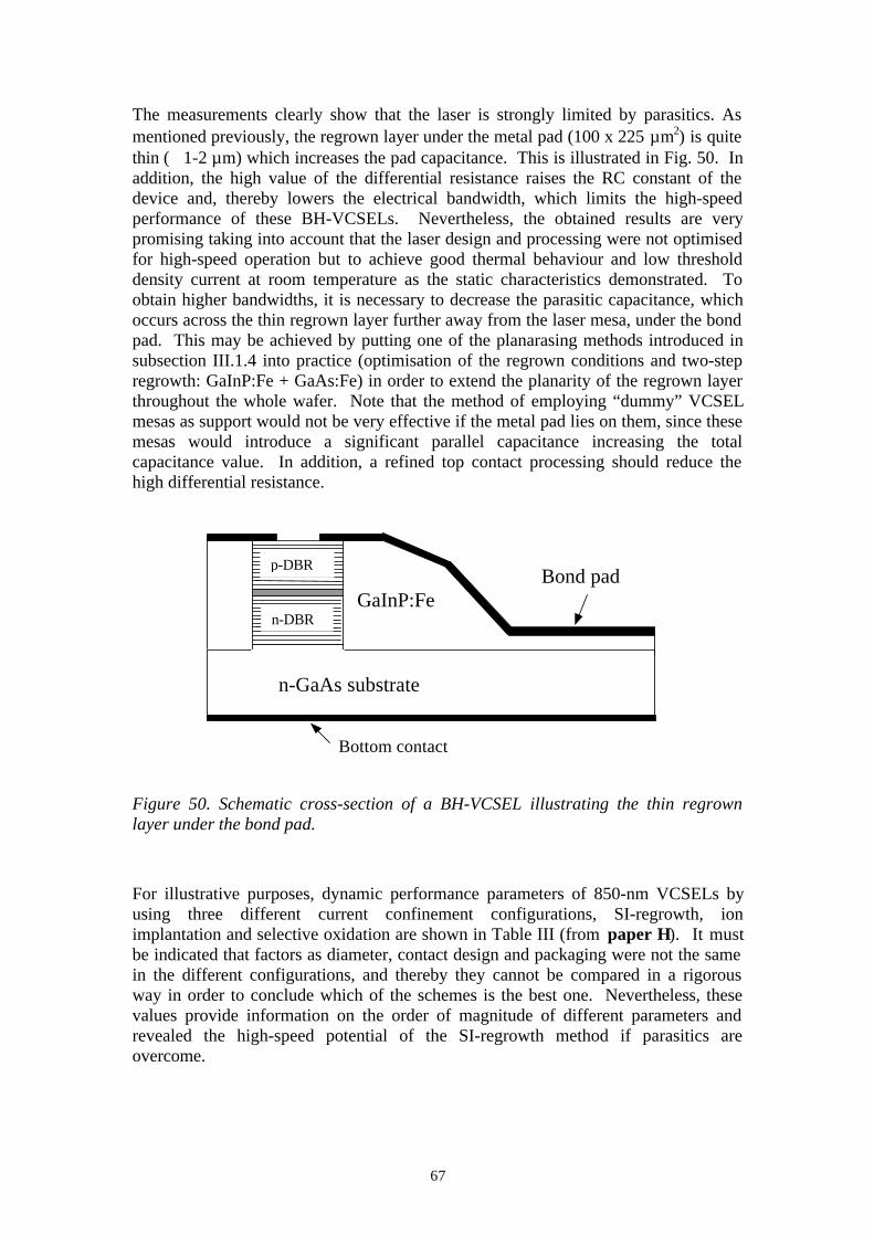
67
The measurements clearly show that the laser is strongly limited by parasitics. Asmentioned previously, the regrown layer under the metal pad (100 x 225 µm2) is quitethin (∼ 1-2 µm) which increases the pad capacitance. This is illustrated in Fig. 50. Inaddition, the high value of the differential resistance raises the RC constant of thedevice and, thereby lowers the electrical bandwidth, which limits the high-speedperformance of these BH-VCSELs. Nevertheless, the obtained results are verypromising taking into account that the laser design and processing were not optimisedfor high-speed operation but to achieve good thermal behaviour and low thresholddensity current at room temperature as the static characteristics demonstrated. Toobtain higher bandwidths, it is necessary to decrease the parasitic capacitance, whichoccurs across the thin regrown layer further away from the laser mesa, under the bondpad. This may be achieved by putting one of the planarasing methods introduced insubsection III.1.4 into practice (optimisation of the regrown conditions and two-stepregrowth: GaInP:Fe + GaAs:Fe) in order to extend the planarity of the regrown layerthroughout the whole wafer. Note that the method of employing “dummy” VCSELmesas as support would not be very effective if the metal pad lies on them, since thesemesas would introduce a significant parallel capacitance increasing the totalcapacitance value. In addition, a refined top contact processing should reduce thehigh differential resistance.
Figure 50. Schematic cross-section of a BH-VCSEL illustrating the thin regrownlayer under the bond pad.
For illustrative purposes, dynamic performance parameters of 850-nm VCSELs byusing three different current confinement configurations, SI-regrowth, ionimplantation and selective oxidation are shown in Table III (from paper H). It mustbe indicated that factors as diameter, contact design and packaging were not the samein the different configurations, and thereby they cannot be compared in a rigorousway in order to conclude which of the schemes is the best one. Nevertheless, thesevalues provide information on the order of magnitude of different parameters andrevealed the high-speed potential of the SI-regrowth method if parasitics areovercome.
n-GaAs substrate
GaInP:FeBond pad
Bottom contact
n-DBR
p-DBR
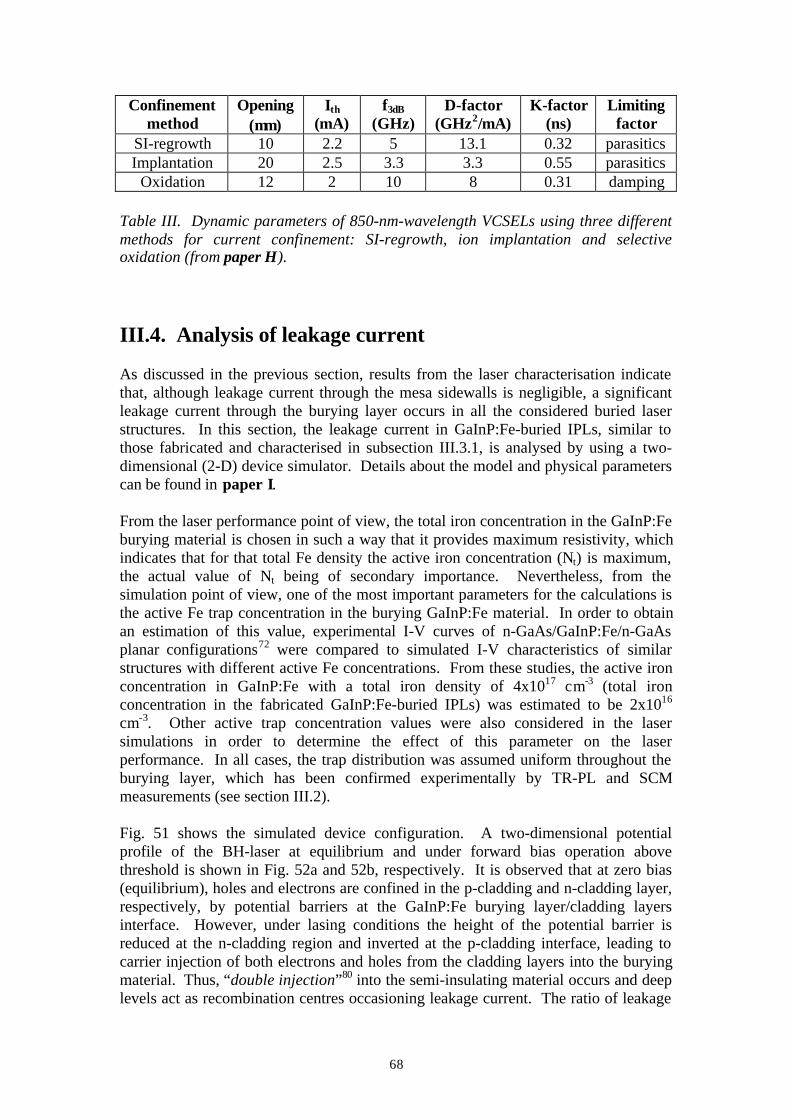
68
Confinementmethod
Opening(µm)
Ith
(mA)f3dB
(GHz)D-factor
(GHz2/mA)K-factor
(ns)Limiting
factorSI-regrowth 10 2.2 5 13.1 0.32 parasiticsImplantation 20 2.5 3.3 3.3 0.55 parasitics
Oxidation 12 2 10 8 0.31 damping
Table III. Dynamic parameters of 850-nm-wavelength VCSELs using three differentmethods for current confinement: SI-regrowth, ion implantation and selectiveoxidation (from paper H).
III.4. Analysis of leakage current
As discussed in the previous section, results from the laser characterisation indicatethat, although leakage current through the mesa sidewalls is negligible, a significantleakage current through the burying layer occurs in all the considered buried laserstructures. In this section, the leakage current in GaInP:Fe-buried IPLs, similar tothose fabricated and characterised in subsection III.3.1, is analysed by using a two-dimensional (2-D) device simulator. Details about the model and physical parameterscan be found in paper I.
From the laser performance point of view, the total iron concentration in the GaInP:Feburying material is chosen in such a way that it provides maximum resistivity, whichindicates that for that total Fe density the active iron concentration (Nt) is maximum,the actual value of Nt being of secondary importance. Nevertheless, from thesimulation point of view, one of the most important parameters for the calculations isthe active Fe trap concentration in the burying GaInP:Fe material. In order to obtainan estimation of this value, experimental I-V curves of n-GaAs/GaInP:Fe/n-GaAsplanar configurations72 were compared to simulated I-V characteristics of similarstructures with different active Fe concentrations. From these studies, the active ironconcentration in GaInP:Fe with a total iron density of 4x1017 cm-3 (total ironconcentration in the fabricated GaInP:Fe-buried IPLs) was estimated to be 2x10¹⁶
cm-3. Other active trap concentration values were also considered in the lasersimulations in order to determine the effect of this parameter on the laserperformance. In all cases, the trap distribution was assumed uniform throughout theburying layer, which has been confirmed experimentally by TR-PL and SCMmeasurements (see section III.2).
Fig. 51 shows the simulated device configuration. A two-dimensional potentialprofile of the BH-laser at equilibrium and under forward bias operation abovethreshold is shown in Fig. 52a and 52b, respectively. It is observed that at zero bias(equilibrium), holes and electrons are confined in the p-cladding and n-cladding layer,respectively, by potential barriers at the GaInP:Fe burying layer/cladding layersinterface. However, under lasing conditions the height of the potential barrier isreduced at the n-cladding region and inverted at the p-cladding interface, leading tocarrier injection of both electrons and holes from the cladding layers into the buryingmaterial. Thus, “double injection”80 into the semi-insulating material occurs and deeplevels act as recombination centres occasioning leakage current. The ratio of leakage
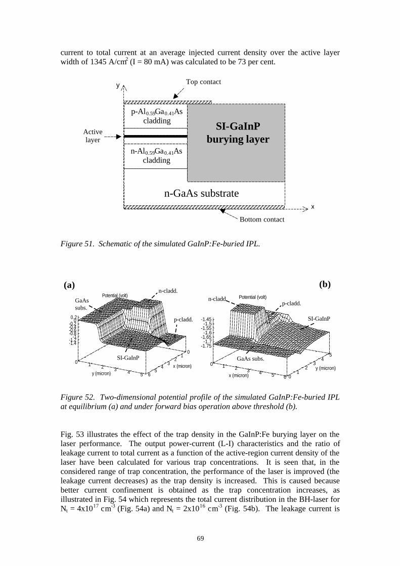
69
current to total current at an average injected current density over the active layerwidth of 1345 A/cm2 (I = 80 mA) was calculated to be 73 per cent.
Figure 51. Schematic of the simulated GaInP:Fe-buried IPL.
Figure 52. Two-dimensional potential profile of the simulated GaInP:Fe-buried IPLat equilibrium (a) and under forward bias operation above threshold (b).
Fig. 53 illustrates the effect of the trap density in the GaInP:Fe burying layer on thelaser performance. The output power-current (L-I) characteristics and the ratio ofleakage current to total current as a function of the active-region current density of thelaser have been calculated for various trap concentrations. It is seen that, in theconsidered range of trap concentration, the performance of the laser is improved (theleakage current decreases) as the trap density is increased. This is caused becausebetter current confinement is obtained as the trap concentration increases, asillustrated in Fig. 54 which represents the total current distribution in the BH-laser forNt = 4x1017 cm-3 (Fig. 54a) and Nt = 2x1016 cm-3 (Fig. 54b). The leakage current is
File:bhgainp17r.plt
01
23
45
6
x (micron) 0 1 2 3 4 5y (micron)
-1.4-1.2
-1-0.8-0.6-0.4-0.2
00.2
Potential (volt)
SI-GaInP
n-cladd.
GaAssubs.
p-cladd.
File:bhgainp17r.plt
0 1 2 3 4 5 6x (micron) 01
23
45
y (micron)
-1.75-1.7
-1.65-1.6
-1.55-1.5
-1.45
Potential (volt)
SI-GaInP
n-cladd.
GaAs subs.
p-cladd.
(a) (b)
SI-GaInPburying layer
n-GaAs substrate
n-Al0.59Ga0.41Ascladding
p-Al0.59Ga0.41Ascladding
Activelayer
Top contact
Bottom contact
y
x
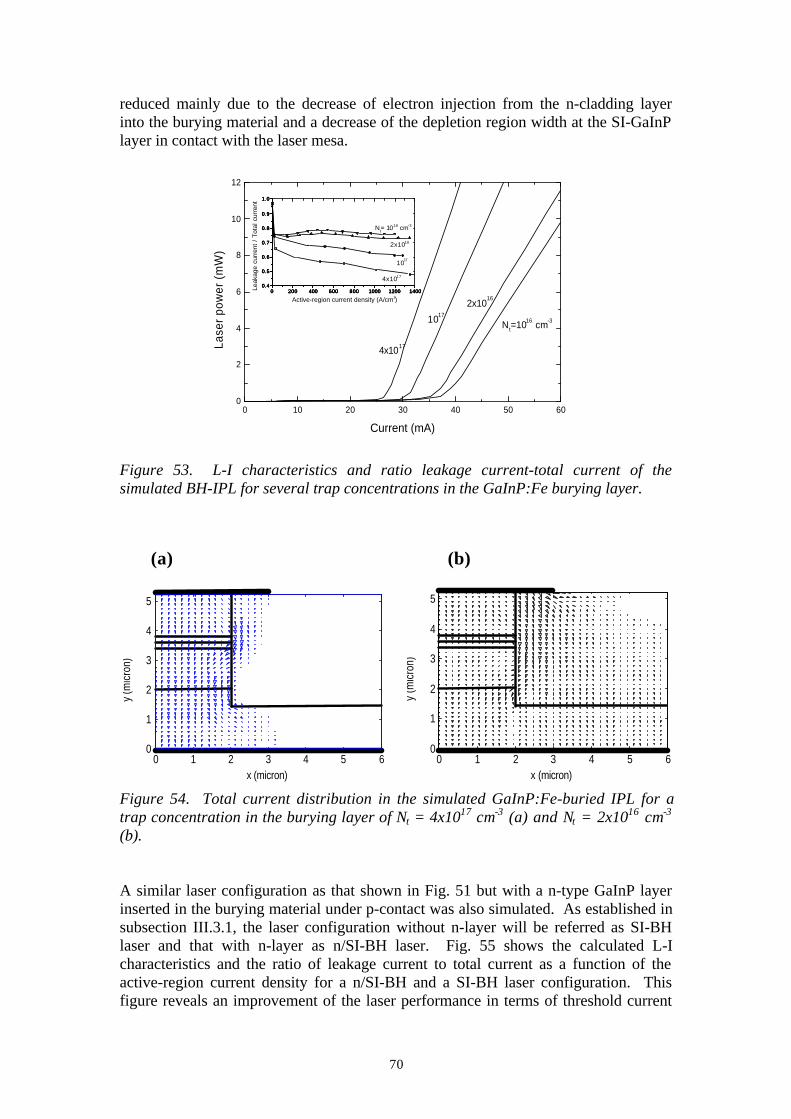
70
reduced mainly due to the decrease of electron injection from the n-cladding layerinto the burying material and a decrease of the depletion region width at the SI-GaInPlayer in contact with the laser mesa.
Figure 53. L-I characteristics and ratio leakage current-total current of thesimulated BH-IPL for several trap concentrations in the GaInP:Fe burying layer.
Figure 54. Total current distribution in the simulated GaInP:Fe-buried IPL for atrap concentration in the burying layer of Nt = 4x1017 cm-3 (a) and Nt = 2x1016 cm-3
(b).
A similar laser configuration as that shown in Fig. 51 but with a n-type GaInP layerinserted in the burying material under p-contact was also simulated. As established insubsection III.3.1, the laser configuration without n-layer will be referred as SI-BHlaser and that with n-layer as n/SI-BH laser. Fig. 55 shows the calculated L-Icharacteristics and the ratio of leakage current to total current as a function of theactive-region current density for a n/SI-BH and a SI-BH laser configuration. Thisfigure reveals an improvement of the laser performance in terms of threshold current
0 10 20 30 40 50 600
2
4
6
8
10
12
4x10¹⁷
1017
2x10¹⁶
N t=1016 cm-3
Lase
r po
wer
(m
W)
Current (mA)
0
1
2
3
4
5
0 1 2 3 4 5 6
y (m
icro
n)
x (micron)
0
1
2
3
4
5
0 1 2 3 4 5 6
y (m
icro
n)
x (micron)
(a) (b)
0 200 400 600 800 1000 1200 14000.4
0.5
0.6
0.7
0.8
0.9
1.0
4x10¹⁷
1017
2x10¹⁶
Nt= 1016 cm-3
0 200 400 600 800 1000 1200 14000.4
0.5
0.6
0.7
0.8
0.9
1.0
Leak
age
curr
ent
/ T
otal
cur
rent
Active-region current density (A/cm2)0 200 400 600 800 1000 1200 1400
0.4
0.5
0.6
0.7
0.8
0.9
1.0
0 200 400 600 800 1000 1200 14000.4
0.5
0.6
0.7
0.8
0.9
1.0
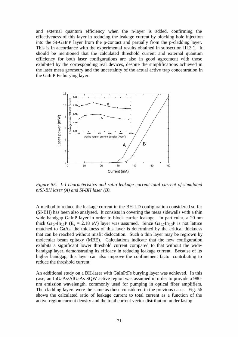
71
and external quantum efficiency when the n-layer is added, confirming theeffectiveness of this layer in reducing the leakage current by blocking hole injectioninto the SI-GaInP layer from the p-contact and partially from the p-cladding layer.This is in accordance with the experimental results obtained in subsection III.3.1. Itshould be mentioned that the calculated threshold current and external quantumefficiency for both laser configurations are also in good agreement with thoseexhibited by the corresponding real devices, despite the simplifications achieved inthe laser mesa geometry and the uncertainty of the actual active trap concentration inthe GaInP:Fe burying layer.
Figure 55. L-I characteristics and ratio leakage current-total current of simulatedn/SI-BH laser (A) and SI-BH laser (B).
A method to reduce the leakage current in the BH-LD configuration considered so far(SI-BH) has been also analysed. It consists in covering the mesa sidewalls with a thinwide-bandgap GaInP layer in order to block carrier leakage. In particular, a 20-nmthick Ga0.7In0.3P (Eg = 2.18 eV) layer was assumed. Since Ga0.7In0.3P is not latticematched to GaAs, the thickness of this layer is determined by the critical thicknessthat can be reached without misfit dislocation. Such a thin layer may be regrown bymolecular beam epitaxy (MBE). Calculations indicate that the new configurationexhibits a significant lower threshold current compared to that without the wide-bandgap layer, demonstrating its efficacy in reducing leakage current. Because of itshigher bandgap, this layer can also improve the confinement factor contributing toreduce the threshold current.
An additional study on a BH-laser with GaInP:Fe burying layer was achieved. In thiscase, an InGaAs/AlGaAs SQW active region was assumed in order to provide a 980-nm emission wavelength, commonly used for pumping in optical fiber amplifiers.The cladding layers were the same as those considered in the previous cases. Fig. 56shows the calculated ratio of leakage current to total current as a function of theactive-region current density and the total current vector distribution under lasing
0 10 20 30 40 50 600
2
4
6
8
10
12
BALase
r po
wer
(m
W)
Current (mA)
200 400 600 800 1000 12000.60
0.65
0.70
0.75
0.80
B
A
Leak
age
curr
ent/T
otal
cur
rent
Active region current density (A/cm2)200 400 600 800 1000 1200
0.60
0.65
0.70
0.75
0.80
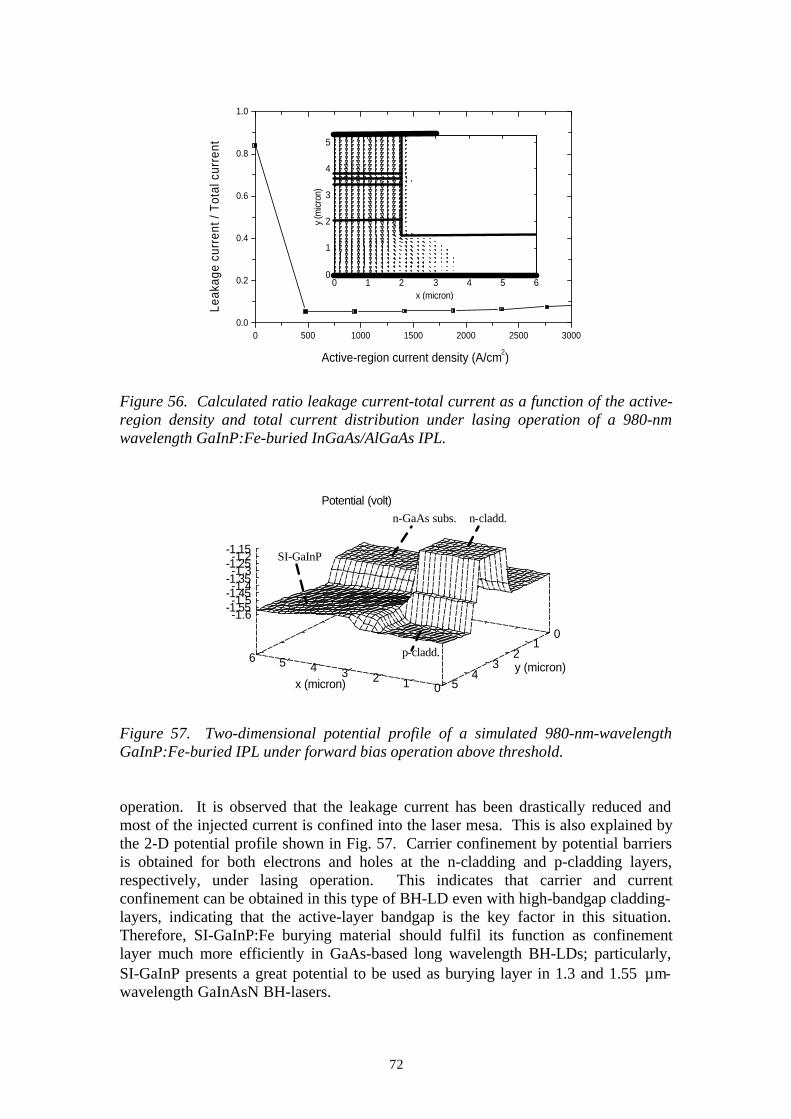
72
Figure 56. Calculated ratio leakage current-total current as a function of the active-region density and total current distribution under lasing operation of a 980-nmwavelength GaInP:Fe-buried InGaAs/AlGaAs IPL.
Figure 57. Two-dimensional potential profile of a simulated 980-nm-wavelengthGaInP:Fe-buried IPL under forward bias operation above threshold.
operation. It is observed that the leakage current has been drastically reduced andmost of the injected current is confined into the laser mesa. This is also explained bythe 2-D potential profile shown in Fig. 57. Carrier confinement by potential barriersis obtained for both electrons and holes at the n-cladding and p-cladding layers,respectively, under lasing operation. This indicates that carrier and currentconfinement can be obtained in this type of BH-LD even with high-bandgap cladding-layers, indicating that the active-layer bandgap is the key factor in this situation.Therefore, SI-GaInP:Fe burying material should fulfil its function as confinementlayer much more efficiently in GaAs-based long wavelength BH-LDs; particularly,SI-GaInP presents a great potential to be used as burying layer in 1.3 and 1.55 µm-wavelength GaInAsN BH-lasers.
0 500 1000 1500 2000 2500 30000.0
0.2
0.4
0.6
0.8
1.0
Leak
age
curr
ent /
Tot
al c
urre
nt
Active-region current density (A/cm2)
0
1
2
3
4
5
0 1 2 3 4 5 6
y (m
icro
n)
x (micron)
File:bhgainp19r.plt
0123456
x (micron)
01
23
45
y (micron)
-1.6-1.55-1.5-1.45-1.4-1.35-1.3-1.25-1.2-1.15
Potential (volt) n-GaAs subs. n-cladd.
SI-GaInP
p-cladd.

73
Finally, it should be mentioned that although no calculations on GaAs:Fe-buriedGaAs/AlGaAs IPLs were achieved, the above discussion suggests that an even higherleakage current should be expected in these lasers. The lower bandgap of GaAs,compared to GaInP, would allow a higher injection of both electrons and holes intothe GaAs:Fe burying layer assuming the same basic laser structure. This wouldexplain the experimental results obtained in subsection III.3.1.B) where the active-layer bandgap (1.45 eV) was even larger than that of GaAs:Fe, leading to a promptcarrier overflow from the cladding layers into the burying material. Nevertheless,further studies should be carried out in order to analyse double injection phenomenain GaAs:Fe, taking into account the existence of two deep trap levels of differentnature: Fe impurities and EL2 defects.
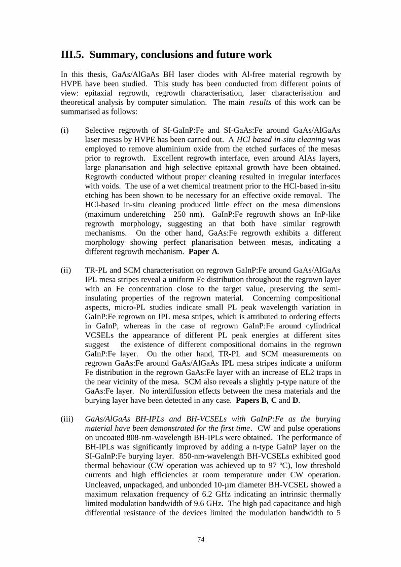
74
III.5. Summary, conclusions and future work
In this thesis, GaAs/AlGaAs BH laser diodes with Al-free material regrowth byHVPE have been studied. This study has been conducted from different points ofview: epitaxial regrowth, regrowth characterisation, laser characterisation andtheoretical analysis by computer simulation. The main results of this work can besummarised as follows:
(i) Selective regrowth of SI-GaInP:Fe and SI-GaAs:Fe around GaAs/AlGaAslaser mesas by HVPE has been carried out. A HCl based in-situ cleaning wasemployed to remove aluminium oxide from the etched surfaces of the mesasprior to regrowth. Excellent regrowth interface, even around AlAs layers,large planarisation and high selective epitaxial growth have been obtained.Regrowth conducted without proper cleaning resulted in irregular interfaceswith voids. The use of a wet chemical treatment prior to the HCl-based in-situetching has been shown to be necessary for an effective oxide removal. TheHCl-based in-situ cleaning produced little effect on the mesa dimensions(maximum underetching ∼250 nm). GaInP:Fe regrowth shows an InP-likeregrowth morphology, suggesting an that both have similar regrowthmechanisms. On the other hand, GaAs:Fe regrowth exhibits a differentmorphology showing perfect planarisation between mesas, indicating adifferent regrowth mechanism. Paper A.
(ii) TR-PL and SCM characterisation on regrown GaInP:Fe around GaAs/AlGaAsIPL mesa stripes reveal a uniform Fe distribution throughout the regrown layerwith an Fe concentration close to the target value, preserving the semi-insulating properties of the regrown material. Concerning compositionalaspects, micro-PL studies indicate small PL peak wavelength variation inGaInP:Fe regrown on IPL mesa stripes, which is attributed to ordering effectsin GaInP, whereas in the case of regrown GaInP:Fe around cylindricalVCSELs the appearance of different PL peak energies at different sitessuggest the existence of different compositional domains in the regrownGaInP:Fe layer. On the other hand, TR-PL and SCM measurements onregrown GaAs:Fe around GaAs/AlGaAs IPL mesa stripes indicate a uniformFe distribution in the regrown GaAs:Fe layer with an increase of EL2 traps inthe near vicinity of the mesa. SCM also reveals a slightly p-type nature of theGaAs:Fe layer. No interdifussion effects between the mesa materials and theburying layer have been detected in any case. Papers B, C and D.
(iii) GaAs/AlGaAs BH-IPLs and BH-VCSELs with GaInP:Fe as the buryingmaterial have been demonstrated for the first time. CW and pulse operationson uncoated 808-nm-wavelength BH-IPLs were obtained. The performance ofBH-IPLs was significantly improved by adding a n-type GaInP layer on theSI-GaInP:Fe burying layer. 850-nm-wavelength BH-VCSELs exhibited goodthermal behaviour (CW operation was achieved up to 97 ºC), low thresholdcurrents and high efficiencies at room temperature under CW operation.Uncleaved, unpackaged, and unbonded 10-µm diameter BH-VCSEL showed amaximum relaxation frequency of 6.2 GHz indicating an intrinsic thermallylimited modulation bandwidth of 9.6 GHz. The high pad capacitance and highdifferential resistance of the devices limited the modulation bandwidth to 5
75
GHz. In both IPL and VCSELs, leakage current along the mesa sidewalls hasbeen found negligible, which indicates a good regrowth interface. However,significant leakage current due to current injection from the laser mesa intothe burying layer exists. Papers E, F, G and H. On the other hand, GaAs:Fe-buried IPLs (855-nm-wavelength) did not show laser emission because mostof the injected current flows through the burying material as leakage current.
(iv) Analysis of leakage current in BH-IPLs (808-nm-wavelength) with GaInP:Feburying layer by using a two-dimensional device simulator has been achieved.Calculations confirm experimental results that a significant part of the injectedcurrent passes by the active layer as a leakage current, revealing the leakagemechanism, which is attributed to a reduction and inversion of theconfinement potential barriers at the laser mesa/burying layer interfaces underforward bias operation. Simulations indicate that leakage current decreases asthe active trap density in the GaInP:Fe burying layer increases. The analysisalso shows that the insertion of a n-GaInP layer is effective in reducingleakage current, in agreement with experimental results, Paper I. Finally,simulations on longer emission wavelength (980 nm) lasers suggest that theleakage current should be drastically minimised by reducing the bandgap ofthe active region, which makes GaInP:Fe a promising material to be used inlong-wavelength GaAs-based BH-lasers. These results also explain theperformance of the fabricated GaAs:Fe-buried IPLs in which most of thecurrent is leakage because of the low bandgap of GaAs:Fe.
From these results, it is concluded that the cleaning and regrowth method by HVPEdeveloped in this work is a suitable technique for the fabrication of GaAs/AlGaAs-based BH laser diodes. The laser performance indicates that SI-GaInP:Fe is anappropriate material to be used as burying layer in these type of lasers (850 nm and808 nm emission wavelength). However, GaAs:Fe has not been found to be anefficient blocking layer in 855-nm-wavelength BH IPLs.
The following lines of research are suggested for future work on this subject:
(i) Planar morphology in GaInP:Fe regrowth. This is a key factor in order toachieve high-speed operation due to the reduction of the pad capacitance.Different possibilities can be tried: to modify regrowth parameters, use ofdummy mesas, and two-step regrowth: GaInP:Fe + GaAs:Fe.
(ii) Compositional variation of regrown GaInP. This is an important issue that canaffect the BH-laser performance. Further micro-PL studies may offer acompositional mapping of the regrown GaInP. Effect of factors as regrowthparameters, mesa geometry, and crystallographic direction may be considered.
(iii) Analysis and characterisation of p/SI/p and n/SI/p structures. I-V-Tcharacteristics of these configurations would yield relevant informationregarding the SI nature of GaInP:Fe and GaAs:Fe on hole and electroninjection, and their behaviour as blocking layer in BH-lasers.

76
(iv) Hybrid confinement scheme: selective oxidation + SI-regrowth in GaAs-basedVCSELs. The combination of both techniques may improve the laserperformance by taking advantage of the benefits from each method.
(v) Long wavelength GaAs-based BH-lasers. GaInP:Fe and GaAs:Fe arepromising materials to be used as confinement layers in 0.980, 1.3 and 1.55µm emission wavelength GaIn(N)As-based BH-lasers. HVPE may providethick burying layers for high-speed operation in these lasers.
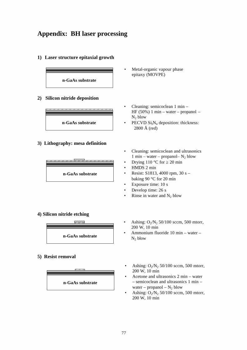
77
Appendix: BH laser processing
1) Laser structure epitaxial growth
2) Silicon nitride deposition
3) Lithography: mesa definition
4) Silicon nitride etching
5) Resist removal
n-GaAs substrate
• Metal-organic vapour phaseepitaxy (MOVPE)
n-GaAs substrate
n-GaAs substrate
• Ashing: O2/N2 50/100 sccm, 500 mtorr,200 W, 10 min
• Acetone and ultrasonics 2 min – water– semicoclean and ultrasonics 1 min –water – propanol – N2 blow
• Ashing: O2/N2 50/100 sccm, 500 mtorr,200 W, 10 min
• Cleaning: semicoclean 1 min –HF (50%) 1 min – water – propanol –N2 blow
• PECVD Si3N4 deposition: thickness:∼2800 Å (red)
• Cleaning: semicoclean and ultrasonics1 min – water – propanol– N2 blow
• Drying 110 °C for ≥ 20 min• HMDS 2 min• Resist: S1813, 4000 rpm, 30 s –
baking 90 °C for 20 min• Exposure time: 10 s• Develop time: 26 s• Rinse in water and N2 blow
• Ashing: O2/N2 50/100 sccm, 500 mtorr,200 W, 10 min
• Ammonium fluoride 10 min – water –N2 blow n-GaAs substrate
n-GaAs substrate
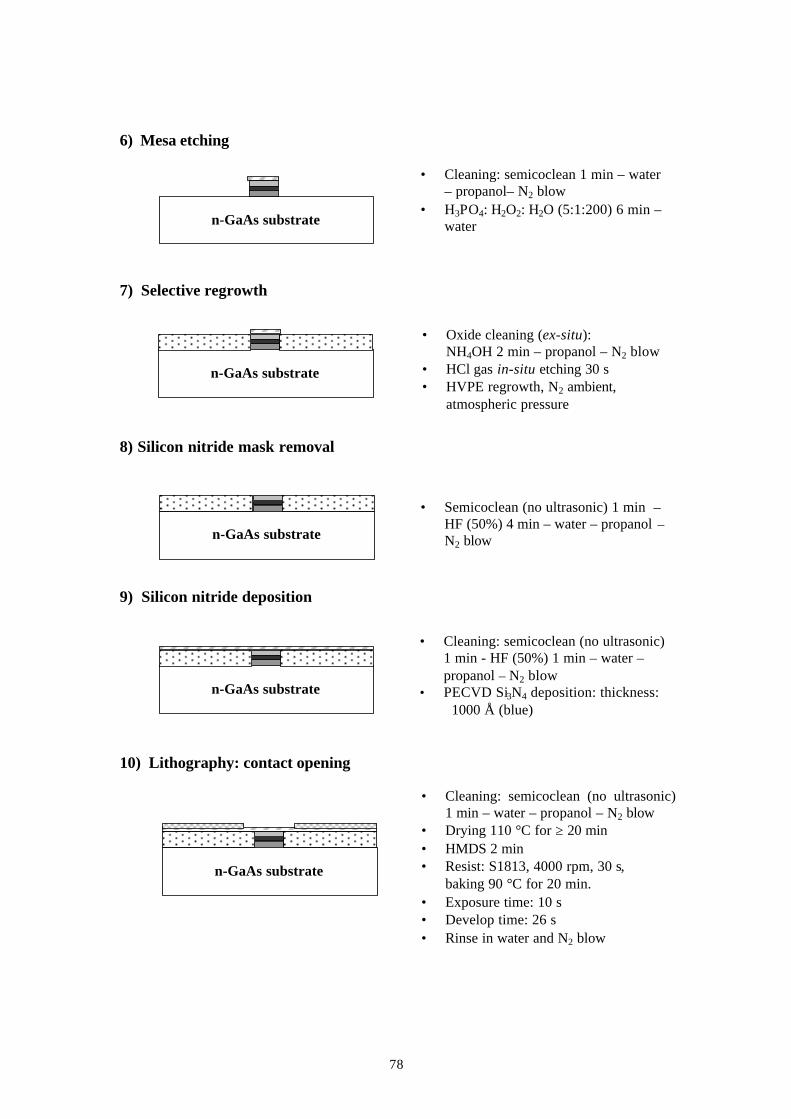
78
6) Mesa etching
7) Selective regrowth
8) Silicon nitride mask removal
9) Silicon nitride deposition
10) Lithography: contact opening
n-GaAs substrate
• Oxide cleaning (ex-situ):NH4OH 2 min – propanol – N2 blow
• HCl gas in-situ etching 30 s• HVPE regrowth, N2 ambient,
atmospheric pressure
• Cleaning: semicoclean 1 min – water– propanol– N2 blow
• H3PO4: H2O2: H2O (5:1:200) 6 min –water
• Semicoclean (no ultrasonic) 1 min –HF (50%) 4 min – water – propanol –N2 blow
• Cleaning: semicoclean (no ultrasonic)1 min - HF (50%) 1 min – water –propanol – N2 blow
• PECVD Si3N4 deposition: thickness:∼1000 Å (blue)
• Cleaning: semicoclean (no ultrasonic)1 min – water – propanol – N2 blow
• Drying 110 °C for ≥ 20 min• HMDS 2 min• Resist: S1813, 4000 rpm, 30 s,
baking 90 °C for 20 min.• Exposure time: 10 s• Develop time: 26 s• Rinse in water and N2 blow
n-GaAs substrate
n-GaAs substrate
n-GaAs substrate
n-GaAs substrate
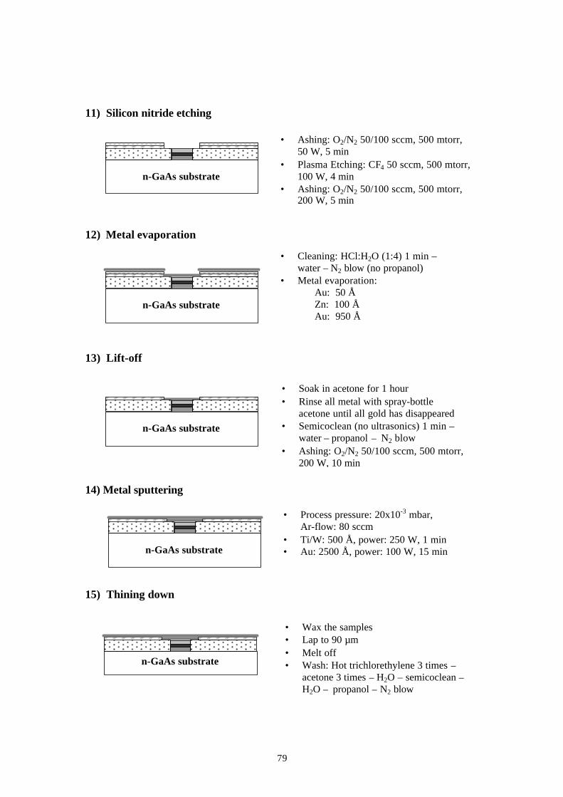
79
11) Silicon nitride etching
12) Metal evaporation
13) Lift-off
14) Metal sputtering
15) Thining down
• Cleaning: HCl:H2O (1:4) 1 min –water – N2 blow (no propanol)
• Metal evaporation:Au: 50 ÅZn: 100 ÅAu: 950 Å
• Soak in acetone for 1 hour• Rinse all metal with spray-bottle
acetone until all gold has disappeared• Semicoclean (no ultrasonics) 1 min –
water – propanol – N2 blow• Ashing: O2/N2 50/100 sccm, 500 mtorr,
200 W, 10 min
n-GaAs substrate
n-GaAs substrate
n-GaAs substrate
• Ashing: O2/N2 50/100 sccm, 500 mtorr,50 W, 5 min
• Plasma Etching: CF4 50 sccm, 500 mtorr,100 W, 4 min
• Ashing: O2/N2 50/100 sccm, 500 mtorr,200 W, 5 min
• Process pressure: 20x10-3 mbar,Ar-flow: 80 sccm
• Ti/W: 500 Å, power: 250 W, 1 min• Au: 2500 Å, power: 100 W, 15 min
• Wax the samples• Lap to 90 µm• Melt off• Wash: Hot trichlorethylene 3 times –
acetone 3 times – H2O – semicoclean –H2O – propanol – N2 blow
n-GaAs substrate
n-GaAs substrate
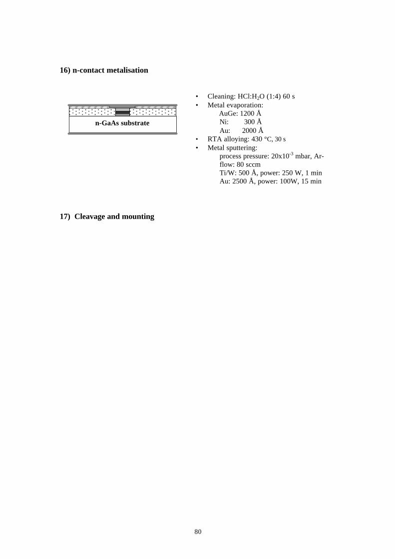
80
16) n-contact metalisation
17) Cleavage and mounting
• Cleaning: HCl:H2O (1:4) 60 s• Metal evaporation:
AuGe: 1200 ÅNi: 300 ÅAu: 2000 Å
• RTA alloying: 430 °C, 30 s• Metal sputtering:
process pressure: 20x10-3 mbar, Ar-flow: 80 sccmTi/W: 500 Å, power: 250 W, 1 minAu: 2500 Å, power: 100W, 15 min
n-GaAs substrate
81
References
1 W.T. Tsang, “High speed photonic devices” in High-Speed Semiconductor Devices,S.M. Sze, ed. New York: John Wiley & Sons, 1990, pp. 587-617.
2 O. Wada, Optoelectronic Integration: Physics, Technology and Applications,Boston: Kluwer, 1994, pp. 1-16.
3 L.A. Coldren and S.W. Corzine, Diode Lasers and Photonic Integrated Circuits,Wiley Series in Microwave and Optical Engineering, John Wiley & sons, Inc. NY(1995).
4 R. Ramaswami and K.N. Sivarajan, Optical Networks – A Practical Perspective,Morgan Kaufman Publishers, Inc., California (1998).
5 A. Yariv, Optical Electronics, Fourth Edition, Saunders College Publishing, 1991, p.572.
6 S. Rapp, K. Streuble, C. Dhollande, J. André, E. Rodríguez Messmer, and S.Lourdudoss, “InP:Fe semi-insulating regrown 1.55 µm vertical cavity lasers based onan integrated InP Bragg reflector,” Optical Society of America, Trends in Optics andPhotonics Series (OSA TOPS), Vol. 15 (Advances in VCSELs), 99-103 (1997).
7 W.W. Chow, K.D. Choquette, M.H. Crawford, K.L. Lear, and G.R. Hadley,“Design, fabrication, and performance of infrared and visible vertical-cavity surface-emitting lasers,” IEEE J. Quantum Electron., vol. 33, pp. 1810-1824, 1997.
8 K Mori, T. Asaka, H. Iwano, M. Ogura, S. Fujii, T. Okada, and S. Mukai, “Effect ofcavity size on lasing characteristics of a distributed Bragg reflector-surface emittinglaser with buried heterostructure,” Appl. Phys. Lett., vol. 60, pp. 21-22, 1992.
9 K. Lear, A. Mar, K.D. Choquette, S.P. Kilcoyne, R.P. Schneider Jr., and K.M. Geib,“High-frequency modulation of oxide-confined vertical cavity surface emittinglasers,” Electron. Lett., vol. 32, pp. 457-458, 1996.
10 C.S. Hong, D. Kasemset, M.E. Kim, and R.A. Milano, “GaAlAs buried-heterostructure lasers grown by a two-step MOCVD process,” Electron. Lett., vol. 19,pp. 759, 1983.
11 Y. Inoue, K. Shimoyama, K. Fujii, N. Hosoi, and H. Gotoh, “Fabrication of AlxGa1-
xAs buried heterostructure laser diodes by in-situ gas etching and selective-areametalorganic vapor phase epitaxy,” J. Cryst. Growth, vol. 145, pp. 881-885, 1994.
12 S. Sugou, Y. Kato, H. Nishimoto, and K. Kasahara, “Planar surface buried-heterostructure InGaAsP/InP lasers with hydride VPE-grown Fe-doped highlyresistive current-blocking layers,” Electron. Lett., vol. 22, pp.1214-1215, Nov. 1986.
13 B.I. Miller, U. Koren, and R.J. Capik, “Planar buried-heterostructure InP/GaInAslasers grown entirely by OMVPE,” Electron. Lett., vol. 22. pp. 947-949, Aug. 1986.
82
14 N.K. Dutta, J.L. Zilko, T. Cella, D.A. Ackerman, T.M. Shen, and S.G. Napholtz,“InGaAsP laser with semi-insulating current confinement layers,” Appl. Phys. Lett.vol. 48, pp.1572-1573, June 1986.
15 S. Lourdudoss, O. Kjebon, J. Wallin, S. Lindgren, IEEE Photon. Technol. Lett. 5(1993) 1119.
16 R. Göbel, F. Steinhagen, H. Janning, Mater. Sci. Eng. B 35 (1995) 59.
17 O. Kjebon, R. Schatz, S. Lourdudoss, S. Nilsson, B. Stålnacke, U. Öhlander, K.Streubel and J. Wallin, SPIE Symp. on Lasers and Integrated Optoelectronics –HighSpeed Semiconductor Laser Sources, USA 1996, paper number 2684-25.
18 P. Morton, R. A. Logan, T. Tanbun-Ek, P.F. Sciortinio Jr., A.M. Sergent, R.K.Montgomery and B.T. Lee, Electron. Lett. 28 (1992) 2156.
19 D. Biswas, N. Debbar, P. Bhattacharya, M. Razegui, M. Defour and F. Omnes,“Conduction- and valence-band offsets in GaAs/Ga0.51In0.49P single quantum wellsgrown by metalorganic chemical vapor deposition,” Appl. Phys. Letters, vol. 56, no.9, pp. 833-835, 1990.
20 M.J. Hafich, J.H. Quigley, R.E. Owens, G.Y. Robinson, D. Li and N. Otsuka,“High quality quantum wells of InGaP/GaAs grown by molecular beam epitaxy,”Appl. Phys. Letters, vol. 54, no. 26, pp. 2686-2688, 1989.
21 J.M. Olson, R.K. Ahrankiel, D.L. Dunlavy, B. Keys and A.E. Kibbler, “Ultralowrecombination velocity at Ga0.5In0.5P/GaAs heterointerfaces,” Appl. Phys. Letters,vol.55, no.12, pp.1208-1210, 1989.
22 M.A. Rao, E.J. Caine, H. Kroemer, S.I. Long and D.I. Babic, ”Determination ofvalence and conduction-band discontinuities at the (Ga,In)P/GaAs heterojunction byC-V profiling,” J. Appl. Phys. vol.61, no.2, 643-649, 1987.
23 Z.L. Liau, S.C. Palmateer, S.H. Groves, J.N. Walpole, L.J. Missagia, Appl. Phys.Lett. 60 (1992) 6.
24 S: Ishikawa, K. Fukagai, H. Chida, T. Miyakazi, H. Fujii, K. Endo, IEEE J.Quantum Electron. 29 (1993) 1936.
25 S. Lourdudoss, R. Holz, O. Kjebon, and G. Landgren, “Iron doped GaInP forselective regrowth around GaAs mesas,” J. Cryst. Growth, vol. 154, pp. 410-414,1995.
26 S. Lourdudoss, A. Ovtchinnikov, O. Kjebon, S. Nilsson, L. Bäckbom, T. Klinga,and R. Holtz, “Entirely aluminum free 905-nm wavelength buried heterostructurelaser by reactive ion etching and semi-insulating GaInP:Fe regrowth,” IEEETransactions on Electron Devices, vol. 44, no.2, February 1997.
83
27 S. Lourdudoss, E. Rodríguez Messmer, O. Kjebon, K. Streubel, J. André, and G.Landgren, Mater. Sci. Eng. B28, 179 (1994).
28 E. Rodríguez Messmer, D. Söderström, P. Hult, S. Marcinkevicius, S. Lourdudoss,and D.C. Look, “Properties of semi-insulating GaAs:Fe grown by hydride vaporphase epitaxy,” J. Electrochem. Soc. 147, 3109 (2000).
29 B.-S. Yoo, H.Y. Chu, H.-H. Park, H.G. Lee, and J. Lee, "Transverse modecharacteristics of vertical-cavity surface emitting lasers buried in amorphous GaAsantiguide layer" IEEE J. Quantum Electron., vol 33, pp.1794-1800, 1997.
30 W.T. Tsang and R.A. Logan, Electron. Lett. 18, 397 (1982).
31 K. Shimoyama, Y. Inoue, M. Katoh, and H. Gotoh, J. Cryst. Growth 107, 767(1991).
32 T. Ohata, K. Honda, S. Hirata, K. Tamamura, H. Ishikawa, K. Miyahara, Y. Mori,and C. Kojima, J. Cryst. Growth 77, 637 (1986).
33 M. Nide, I. Komazaki, K. Kobayashi, K. Endo, M. Ueno, T. Kamejima, and T.Suzuki, IEEE J. Quantum Electron. QE-23, 720 (1987).
34 K.D. Choquette, M. Hong, R.S. Freund, S.N.G. Chu, J.P. Mannaerts, and R.C.Wetzel, Appl. Phys. Lett. 60, 1738 (1992).
35 K.D. Choquette, M. Hong, S.N.G. Chu, H.S. Luftman, J.P. Mannaerts, R.C. Wetzel,and R.S. Freund, “Hydrogen plasma removal of AlGaAs oxides before molecularbeam epitaxy,” Appl. Phys. Lett. 62 (7), 735 (1993).
36 P. Bhattacharya, Semiconductor Optoelectronic Devices, 2nd edition, Prentice Hall,Inc., 1997, p.2.
37 E.P. O’Reilly and A.R. Adams, “Band-structure engineering in strainedsemiconductor lasers,” IEEE J. Quantum Electron. 30, 366-379 (1994).
38 H. Asai and K. Oe, J. Appl. Phys., vol. 54, p. 2052, 1983
39 S. Adachi, “ Material parameters of In1-xGaxAsyP1-y and related binaries,” J. Appl.Phys. vol. 53, pp. 8775-8792, 1982.
40 H.C. Casey, D.D. Sell, M.B. Panish, “Refractive index of AlxGa1-xAs between 1.2and 1.8 eV,” Appl. Phys. Lett. 24, 63-64 (1974).
41 Materials for optoelectronics, edited by Maurice Quillec, Kluwer AcademicPublishers, 1996.
42 M. Kondow, K. Uomi, A. Niwa, T. Kitatani, S. Watahiki, and Y. Yazawa,“GaInNAs: A novel material for long-wavelength range laser diodes with excellenthigh-temperature performance,” Jpn. J. Appl. Phys., vol. 35, pp. 1273-1275, 1996.
84
43 R. Williams, Modern GaAs Processing Methods, Artech House, 1990.
44 H.M Cox, S.G. Hummel, and V.G. Keramidas, J. Cryst. Growth 79 (1986) 900.
45 S. Lourdudoss and O. Kjebon, “Hydride Vapor Phase Epitaxy Revisited,” IEEE J.Selected Topics Quantum Electron. vol. 3, no. 3, June 1997.
46 G.B. Stringfellow, Organometallic Vapor-Phase Epitaxy, Theory and Practice,Academic Press, 1999.
47 Handbook of Crystal Growth, D.T.J. Hurle, Ed., Amsterdam, The Netherlands,Elsevier, 1994.
48 A. Koukitu and H. Seki, “Thermodynamic analysis for InGaAsP epitaxial growthby the chloride-CVD process,” J. Cryst. Growth, vol. 49, pp. 325-333, 1980.
49 N. Gopalakrishnan, R. Dhanasekaran, and S. Lourdudoss, “Compositional analysisof quaternary GaxIn1-xAsyP1-y vapor phase epitaxy: A comparison between theory andexperiment,” Materials Chemistry and Physics, vol. 50, no. 1, pp. 70-75, 1997.
50 D.W. Shaw, “Mechanisms in vapor phase epitaxy,” in Crystal Growth, C.H.L.Goodman, Ed. New York: Plenum, 1974, vol. 1, ch. 1.
51 G.B. Stringfellow, “Fundamentals of thin film growth,” J. Cryst. Growth, vol. 137,pp. 212-223, 1994.
52 B.-T. Lee, R.A. Logan, and S.N.G. Chu, “Observation of growth pattern duringatmospheric pressure metalorganic vapor phase epitaxy regrowth of InP aroundetched mesas,” J. Cryst. Growth, vol. 130, pp. 287-294, 1993.
53 R.W. Glew, J.P. Stagg, P.D. Greene, A.T.R. Briggs, S. Bradshaw, and J.H. Marsh,“Thermal instability of InGaAs/InGaAsP quantum wells,” in 3rd Int. Conf. IndiumPhosphide and Related Materials, Cardiff, U.K., 1991, pp. 515-518.
54 S. Lourdudoss, B. Hammarlund, and O. Kjebon, “An investigation on hydride VPEgrowth and properties of semi-insulating InP:Fe,” J. Electron. Mater., vol. 19, pp.981-987, 1990.
55 E.F. Schubert, Doping in III-V Semiconductors, Cambridge Studies inSemiconductor Physics and Microelectronic Engineering, 1993.
56 R.F. Pierret, Advanced Semiconductor Fundamentals, Modular Series on SolidState Devices, Volume VI, Addison-Wesley, 1987.
57 J. Bourgoin and M. Lannoo, Point Defects in Semiconductors II, Springer-VerlagBerlin Heidelberg New York, 1983.
85
58 D.D. Nolte, “Semi-insulating semiconductor heterostructures: Optoelectronicproperties and applications,” J. Appl. Phys., vol.85, no.9, pp.6259-6289, 1999.
59 P.N. Favennec, G.P. Peblous, M. Binet, and P. Baudet, in Ion Implantation inSemiconductors and other Materials, edited by B.L. Crowder (Plenum, New York,1973), p. 621.
60 A.C. Warren, J.M. Woodall, J.L. Freeouf, D. Grishowsky, D.T. McInturff, M.R.Melloch, and N. Otsuka, Appl. Phys. Lett. 57, 1331 (1990).
61 T. Murotani, T. Shimanoe, and S. Mitsui, J. Cryst. Growth., 45, p. 302, 1978.
62 D.C. Look, Y. He, J. Ramdani, N. El-Masry, and S.M. Bedair, “Semi-insulatingnature of gas source molecular beam epitaxial InGaP grown at very lowtemperatures,” Appl. Phys. Lett., vol. 63, pp.1231-1233, 1993.
63 O. Mizuno and H. Watanabe, “Semi-insulating properties of Fe-doped InP,”Electron. Lett., vol. 11, pp. 118-119, 1975.
64 M.J. Harlow, W.J. Duncan, I.F. Lealman, and P.C. Spurdens, J. Cryst. Growth, 140,p.19, 1994.
65 C.D. Brandt, A.M. Hennel, L.M. Pawlovitcz, Y.-T Wu, T. Bryskiewicz, J.Lagowski, and H.C. Gatos, “New semi-insulating InP:Titanium midgap donors,”Appl. Phys. Lett., vol. 48, pp. 1162-1164, 1986.
66 A. Dadgar, O. Stenzel, L. Köhne, A. Näser, M. Strassburg, W. Stolz, D. Bimbergand H. Schumann, “Growth of Ru doped semi-insulating InP by low pressuremetalorganic chemical vapor deposition,” J. Cryst. Growth, 195, p. 65, 1998.
67 J.A. Long, V.G. Riggs, and W.D. Johnston, J. Cryst. Growth 69, 10 (1984).
68 P.L. Hoyt and R.W. Haisty, “The preparation of epitaxial semi-insulating galliumarsenide by iron doping,” J. Electrochem. Soc., 113, p. 296, 1966.
69 S.J. Bass, J. Cryst. Growth, 44, p. 29, 1978.
70 C.D. Brandt, A.M. Hennel, T. Bryskiewicz, K.Y. Ko, and L.M. Pawlosicz,“Electronic and optical properties of Ti-doped GaAs and InP; semi-insulating InP,” J.Appl. Phys., 65, p. 3459, 1989.
71 B. Tell, U. Koren, and B.I. Miller, “Metalorganic vapor-phase-epitaxial growth ofFe-doped In0.53Ga0.47As,” J. Appl. Phys., 61, p. 1172, 1987.
72 S. Lourdudoss and R. Holtz, “Fabrication and I-V-T behaviour of n-GaAs/semi-insulating GaInP:Fe/n-GaAs structures,” J. Cryst. Growth 179 (1997) 371-381.
86
73 T. Tanahashi, M. Kondo, and M. Sugawara, “Liquid phase epitaxial growth of Fe-doped semi-insulating InP, GaInAsP, and AlGaInAs,” Fujitsi Sci. Tech. J., 24, p. 242,1988.
74 W.T. Tsang and R.A. Logan, Appl. Phys. Lett. 36, p. 730, 1980.
75 M Okayasu, A. Kozem, Y. Hasumi, J. Temmyo, and S. Uehara, Appl. Phys. Lett.51, p. 1980, 1987.
76 D. Söderström, “Epitaxy, analysis and application of semi-insulating III-Vmaterials,” Doctoral dissertation, Royal Institute of Technology, Stockholm, Sweden,2001.
77 M.A. Lampert and P. Mark, Current Injection in Solids, Academic Press, NewYork, 1970.
78 P.J. Corvini, “Current injection in semi-insulating Indium Phosphide,” Doctoraldissertation, ECE Technical Report No. 95-26, University of California at SantaBarbara, 1995.
79 D. Söderström and S. Lourdudoss, “Resistivity analysis on n-SI-n and p-SI-pstructures exemplified with semi-insulating InP,” J. Appl. Phys., vol. 89, p. 4004,2001.
80 M.A. Lampert, “Double injection in insulators,” Phys. Rev., vol. 125, pp. 126-141,Jan. 1986.
81 T. Takanohashi, S. Isozumi, M. Sugawara, and K. Nakajima, “The acceptor level ofFe in In0.49Ga0.51P,” Jpn. J. Appl. Phys., no.7, pp. 1194-1195, July 1987.
82 A. Cesna, D. Söderström, S. Marcinkevicius, and S. Lourdudoss, “Carrier trappingin iron-doped GaInP,” J. Appl. Phys., vol. 85, pp. 1234-1236, Jan 1999.
83 D.T. McInturff, E.S. Harmon, J.C.P. Chang, T.M. Pekarek, and J.M. Woodall,Appl. Phys. Lett., 69, p.1885, 1996.
84 Gray M.L., Peterson L., Tang R-S, Saban S.B. and Blakemore J.S., J. Appl. Phys.,73, p. 3319, 1993.
85 N.D Jager, A.K. Jerma, P. Dreszer, N. Newman, A. Liliental-Weber, and E.R.Weber, J. Electron. Mat. 22, 1499 (1993).
86 Spaeth J.-M, Krambrock K., and Hofman D.M. in 20th Int. Conf. Phys. Semicon.Vol.1, ed. Anastassakis E.M and Joannpoulus J.D. (World Scientific, Singapore), p.441, 1990.
87 Properties of Gallium Arsenide, second edition, Inspec, The institution of ElectricalEngineers, 1990.
87
88 D.V. Lang and R.A. Logan, “A study of deep levels in GaAs by capacitancespectroscopy,” J. Electron. Materials, vol. 4, no. 5, p. 1053, 1975.
89 Kleverman M., Omling P., Lebedo L-A and Grimmeiss H.G., J. Appl. Phys., 54,p.814, 1983.
90 Look D.C. and Fang Z-Q, “Simple measurement of 300 K electron capture crosssection for EL2 in GaAs,” J. Appl. Phys., 80, no.6, p.3590, 1996
91 A. Gomyo and T. Suzuki, “Observation of strong ordering in GaxIn1-xP alloysemiconductors,” Phys. Rev. Lett., vol. 60, no. 25, pp. 2645-2648, 1988.
92 A. Gaarder, S. Marcinkevicius, E. Rodríguez Messmer, and S. Lourdudoss,“Dopant distribution in selectively regrown InP:Fe studied by time-resolvedphotoluminscence,” J. Cryst. Growth, 226, p.451, 2001.
93 S. Anand, “Another dimension in device characterization,” IEEE Circuits andDevices magazine, vol.16, p.12, 2000.
94 G.P. Agrawal and N.K. Dutta, Long-wavelength semiconductor lasers, VanNostrand Reinhold electrical/computer science and engineering series, 1986.
95 Nelson, R.J., R.B. Wilson, P.D. Wrigth, P.A. Barnes, and N.K. Dutta. IEEE J.Quantum Electron. QE-17, 202 (1981).
96 Asbeck, P.M., D.A. Cammack, J.J. Daniele, and V. Klebanoff. IEEE J. QuantumElectron. QE-15, 727 (1979).
97 Agrawal, G.P., J. Lightwave Technol. LT-2, 537 (1984).
98 Casey, H.C., Jr., and E. Buehler. Appl. Phys. Lett. 30, 247 (1977).
99 Y. Yoshida, H. Watanabe, K. Shibata, A. Takemoto, and H. Higuchi, “Theoreticaland experimental analysis of leakage current in InGaAsP BH lasers with p-n-p-ncurrent blocking layers,” J. Quantum Electron. vol. 35, no. 9, September 1999.
100 S. Asada, S. Sugou, K. Kasahara, and S. Kumashiro, “Analysis of leakage currentin buried heterostructure lasers with semiinsulating blocking layers,” IEEE J.Quantum Electron. vol. 25. pp. 1362-1368, 1989.
101 M. Hoshino, K. Kitahara, K. Kodama, and M. Ozeki, “GaInP growth by chloridevapor phase epitaxy,” J. Cryst. Growth, 96, pp. 188-200, 1989.
102 R.V. Holtz, “Growth and characterization of semi-insulating GaInP on planar andnon-planar substrates,” Master thesis, Royal Institute of Technology, Stockholm,Sweden, 1995.
88
103 J.C. Bailar, H.J. Emeléus, R. Nyholm, and A.F. Trotman-Dickenson,Comprehensive Inorganic Chemistry, vol. 1 (Oxford, U.K.: Pergamon Press, 1973), p.1032.
104 C.C. Chang, D.B. Fraser, M.J. Grieco, T.T. Sheng, S.E. Haszko, R.E. Kerwin, R.B.Marcus, and A.K. Sinha, J. Electrochem. Soc., vol.125, no. 5, pp.787-92, 1978.
105 D.A. Allwood, R.T. Carline, N.J. Mason, C. Pickering, B.K. Tanner, and P.J.Walker, Thin Solid Films 364, 33 (2000).
106 E. Rodríguez Messmer, T. Lindström, and S. Lourdudoss, J. Cryst. Growth 210,600 (2000).
107 S. Lourdudoss, E. Rodríguez Messmer, O. Kjebon, and G. Landgren, “Temporallyresolved selective regrowth of InP around [110] and [110] mesas,” J. Electron. Mat.vol. 25, no. 3, p.389, 1996.
108 P. Hult, “Properties and selective epitaxy of semi-insulating GaAs:Fe,” Masterthesis, Royal Institute of Technology, Stockholm, Sweden, 1999.
109 K. Tateno, H. Uenohara, T. Kagawa, and C. Amano, “Characteristics of the GaInPlayers grown by metalorganic chemical vapor deposition on mesa-patterned GaAssubstrates,” J. Cryst. Growth 209 (2000) 605-613.
110 S. Lourdudoss, E. Rodríguez Messmer, O. Kjebon, and G. Landgren, J. Cryst.Growth 154, 410 (1995).
111 E. Rodríguez Messmer and S. Lourdudoss, “Analysis of regrowth evolution aroundVCSEL type mesas,” J. Cryst. Growth 219 (2000), p.185.
112 J.J. O’Shea, C.M Reaves, and S.P. DenBaars, “Conduction band offsets in ordered-GaInP/GaAs heterostructures studied by ballistic-electron-emission microscopy,”Appl. Phys. Lett., 69 (20), pp. 3022-3024, 1996.
113 M.C. DeLong et al., Appl. Phys. Lett. 66, 3185 (1995); AIP Conf. Proc. 306, 529(1994).
114 B.T. McDermott, N.A. El-Masry, B.L. Jiang, F. Hyuga, and S.M. Bedair, “OrderedGaInP by atomic layer epitaxy,” J. Cryst. Growth 107 (1991) 96-101.
115 O. Douhéret et al. to be submitted
116 Anthony, P.J., T.L. Paoli, and R.L. Hartman. IEEE J. Quantum Electron. QE-16,735 (1980).
117 M. Schubert, J.A. Woollam, G. Leibiger, B. Rheinländer, I. Pietzonka, T. Sab, andB. Gottschalch, “Isotropic dielectric functions of highly disordered AlxGa1-xInP(0≤x≤1) lattice matched to GaAs,” J. Appl. Phys. vol. 86, 4, pp. 2025-2033, 1999.
89
118 S. Adachi, “GaAs, AlAs, and AlxGa1-xAs: Material parameters for use in researchand device applications,” J. Appl. Phys. 58 (3), 1 August 1985.
119 D.F. Welch, P.S. Cross, and D.R. Scifres, “Properties of AlGaAs buriedheterostructure lasers and laser arrays grown by a two-step metalorganic chemicalvapor deposition,” Appl. Phys. Lett. 48 (25), p. 1716, 1986.
120 X.A. Cao, J.R. LaRoche, F. Ren, S.J. Pearton, J.R. Lothian, R.K. Singh, R.G.Wilson, H.J. Guo, and S.J. Pennycook, “Implanted p-n junctions in GaN,” Solid-StateElectron. 43 (1999) 1235-1238.
121 H. Uenohara, K. Tateno, T. Kagawa, and C. Amano, “All MOCVD grown 850-nm-wavelength refractive-index-guided semiconductor-buried vertical-cavity surface-emitting lasers with p/n-InGaP current blocking layers,” IEEE Photon. Technol. Lett.,vol. 12, no. 6, p.600, 2000.
122 C.J. Chang-Hasnain, Y.-A. Wu, G.S. Li, G. Hasnain, K.D. Choquette, C. Caneau,L.T. Florez, “Low threshold buried heterostructure vertical-cavity surface-emittinglaser,” Conf. on Lasers and Electro-Optics (CLEO), Tech. Dig. Ser., 11, 136 (1993).
123 K.D. Choquette, M. Hong, R.S. Freund, J.P. Mannaerts, R.C. Wetzel, and R.W.Leibenguth, “Vertical-cavity surface-emitting laser diodes fabricated by in situ dryetching and molecular beam epitaxial regrowth,” IEEE Photon. Technol. Lett., vol. 5,no. 3, p.284, 1993.
124 G.R. Hadley, K.L. Lear, M.E. Warren, K.D. Choquette, J.W. Scott, and S.W.Corzine, “Comprehensive numerical modeling of vertical-cavity surface-emittinglasers,” IEEE J. Quantum Electron., vol.32, pp.607-616, 1996.