GaAs, pHEMT, MMIC, Single Positive Supply, DC to … · 1 1 NIC 10 NIC 13 V GG 1 14 NIC 15 ACG3 16...
21
GaAs, pHEMT, MMIC, Single Positive Supply, DC to 7.5 GHz, 1 W Power Amplifier Data Sheet HMC637BPM5E Rev. 0 Document Feedback Information furnished by Analog Devices is believed to be accurate and reliable. However, no responsibility is assumed by Analog Devices for its use, nor for any infringements of patents or other rights of third parties that may result from its use. Specifications subject to change without notice. No license is granted by implication or otherwise under any patent or patent rights of Analog Devices. Trademarks and registered trademarks are the property of their respective owners. One Technology Way, P.O. Box 9106, Norwood, MA 02062-9106, U.S.A. Tel: 781.329.4700 ©2018 Analog Devices, Inc. All rights reserved. Technical Support www.analog.com FEATURES P1dB output power: 28 dBm typical Gain: 15.5 dB typical Output IP3: 39 dBm typical Self biased at VDD = 12 V at 345 mA typical Optional bias control on VGG1 for IDQ adjustment Optional bias control on VGG2 for IP2 and IP3 optimization 50 Ω matched input/output 32-lead, 5 mm × 5 mm LFCSP package: 25 mm 2 APPLICATIONS Military and space Test instrumentation FUNCTIONAL BLOCK DIAGRAM 17 1 3 4 2 9 GND V GG 2 NIC GND 5 6 RFIN GND 7 NIC 8 GND GND PACKAGE BASE GND 18 NIC 19 NIC 20 GND 21 RFOUT/V DD 22 GND 23 NIC 24 GND GND 12 NIC 11 NIC 10 NIC 13 V GG 1 14 NIC 15 ACG3 16 GND 25 GND 26 NIC 27 NIC 28 NIC 29 ACG2 30 ACG1 31 NIC 32 GND 16273-001 Figure 1. GENERAL DESCRIPTION The HMC637BPM5E is a gallium arsenide (GaAs), monolithic microwave integrated circuit (MMIC), pseudomorphic high electron mobility transistor (pHEMT), cascode distributed power amplifier. The device is self biased in normal operation and features optional bias control for quiescent current (IDQ) adjustment and for second-order intercept (IP2) and third-order intercept (IP3) optimization. The amplifier operates from dc to 7.5 GHz, providing 15.5 dB of small signal gain, 28 dBm output power at 1 dB gain compression, a typical output IP3 of 39 dBm, and a 3.5 dB noise figure, while requiring 345 mA from a 12 V supply voltage (VDD). Gain flatness is excellent from dc to 7.5 GHz at ±0.5 dB typical, making the HMC637BPM5E ideal for military, space, and test equipment applications. The HMC637BPM5E also features inputs/outputs (I/Os) that are internally matched to 50 Ω, housed in a RoHS-compliant, 5 mm × 5 mm, premolded cavity, lead frame chip scale package (LFCSP), making the device compatible with high volume, surface-mount technology (SMT) assembly equipment.
Transcript of GaAs, pHEMT, MMIC, Single Positive Supply, DC to … · 1 1 NIC 10 NIC 13 V GG 1 14 NIC 15 ACG3 16...
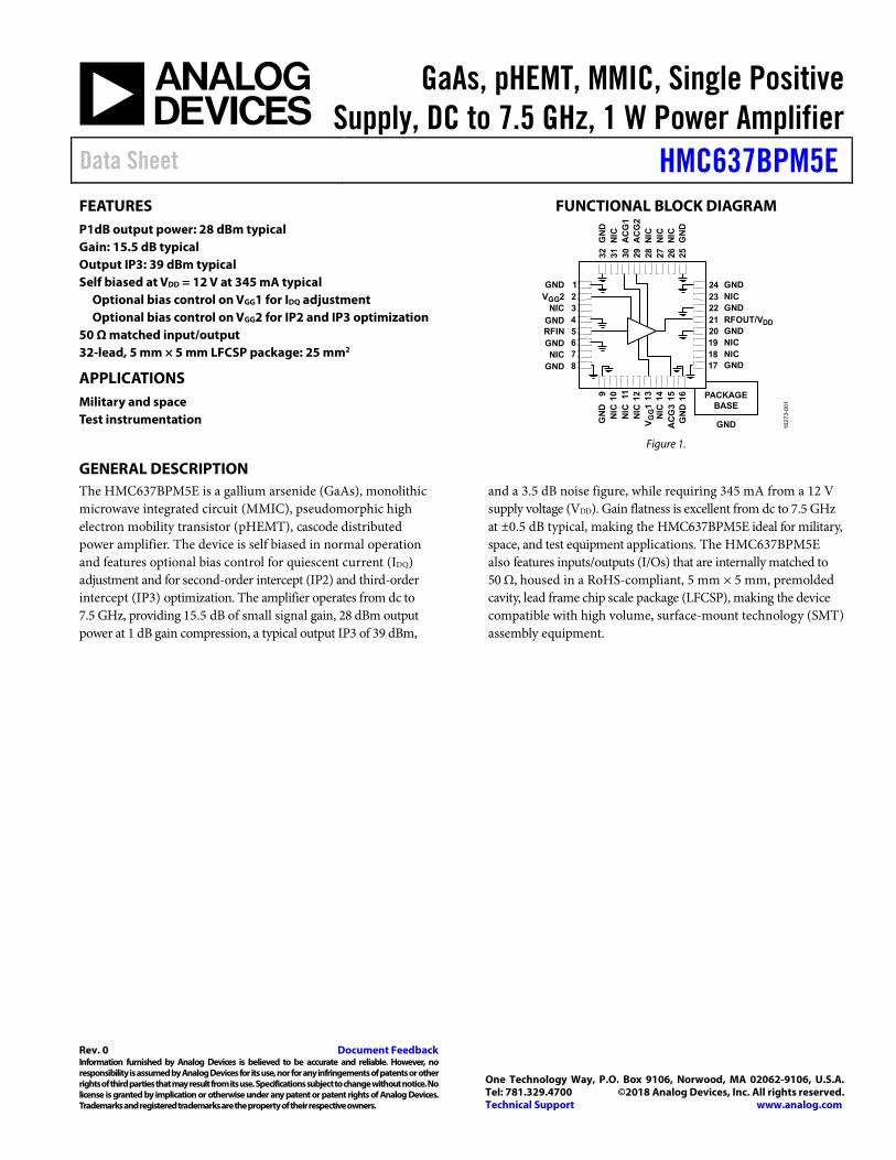
GaAs, pHEMT, MMIC, Single Positive Supply, DC to 7.5 GHz, 1 W Power Amplifier
Data Sheet HMC637BPM5E
Rev. 0 Document Feedback Information furnished by Analog Devices is believed to be accurate and reliable. However, no responsibility is assumed by Analog Devices for its use, nor for any infringements of patents or other rights of third parties that may result from its use. Specifications subject to change without notice. No license is granted by implication or otherwise under any patent or patent rights of Analog Devices. Trademarks and registered trademarks are the property of their respective owners.
One Technology Way, P.O. Box 9106, Norwood, MA 02062-9106, U.S.A. Tel: 781.329.4700 ©2018 Analog Devices, Inc. All rights reserved. Technical Support www.analog.com
FEATURES P1dB output power: 28 dBm typical Gain: 15.5 dB typical Output IP3: 39 dBm typical Self biased at VDD = 12 V at 345 mA typical
Optional bias control on VGG1 for IDQ adjustment Optional bias control on VGG2 for IP2 and IP3 optimization
50 Ω matched input/output 32-lead, 5 mm × 5 mm LFCSP package: 25 mm2
APPLICATIONS Military and space Test instrumentation
FUNCTIONAL BLOCK DIAGRAM
17
1
34
2
9
GNDVGG2
NICGND
56
RFINGND
7NIC8GND GND
PACKAGEBASE
GND
18 NIC19 NIC20 GND21 RFOUT/VDD
22 GND23 NIC24 GND
GN
D
12N
IC11
NIC
10N
IC
13V G
G1
14N
IC15
AC
G3
16G
ND
25G
ND
26N
IC27
NIC
28N
IC29
AC
G2
30A
CG
131
NIC
32G
ND
1627
3-00
1
Figure 1.
GENERAL DESCRIPTION The HMC637BPM5E is a gallium arsenide (GaAs), monolithic microwave integrated circuit (MMIC), pseudomorphic high electron mobility transistor (pHEMT), cascode distributed power amplifier. The device is self biased in normal operation and features optional bias control for quiescent current (IDQ) adjustment and for second-order intercept (IP2) and third-order intercept (IP3) optimization. The amplifier operates from dc to 7.5 GHz, providing 15.5 dB of small signal gain, 28 dBm output power at 1 dB gain compression, a typical output IP3 of 39 dBm,
and a 3.5 dB noise figure, while requiring 345 mA from a 12 V supply voltage (VDD). Gain flatness is excellent from dc to 7.5 GHz at ±0.5 dB typical, making the HMC637BPM5E ideal for military, space, and test equipment applications. The HMC637BPM5E also features inputs/outputs (I/Os) that are internally matched to 50 Ω, housed in a RoHS-compliant, 5 mm × 5 mm, premolded cavity, lead frame chip scale package (LFCSP), making the device compatible with high volume, surface-mount technology (SMT) assembly equipment.

HMC637BPM5E Data Sheet
Rev. 0 | Page 2 of 21
TABLE OF CONTENTS Features .............................................................................................. 1 Applications ....................................................................................... 1 Functional Block Diagram .............................................................. 1 General Description ......................................................................... 1 Revision History ............................................................................... 2 Specifications ..................................................................................... 3
Frequency Range = DC to 7.5 GHz ........................................... 3 Absolute Maximum Ratings ............................................................ 4
Thermal Resistance ...................................................................... 4 ESD Caution .................................................................................. 4
Pin Configuration and Function Descriptions ............................. 5
Interface Schematics .....................................................................6 Typical Performance Characteristic ................................................7 Theory of Operation ...................................................................... 17 Applications Information .............................................................. 18
Typical Application Circuit ....................................................... 19 Evaluation PCB ............................................................................... 20
Bill of Materials ........................................................................... 20 Outline Dimensions ....................................................................... 21
Ordering Guide .......................................................................... 21
REVISION HISTORY 5/2018—Revision 0: Initial Version
Data Sheet HMC637BPM5E
Rev. 0 | Page 3 of 21
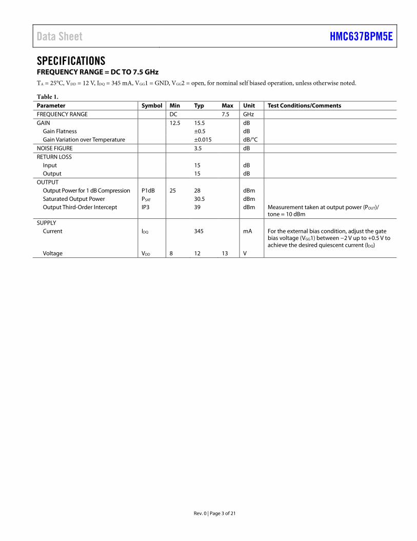
SPECIFICATIONS FREQUENCY RANGE = DC TO 7.5 GHz TA = 25°C, VDD = 12 V, IDQ = 345 mA, VGG1 = GND, VGG2 = open, for nominal self biased operation, unless otherwise noted.
Table 1. Parameter Symbol Min Typ Max Unit Test Conditions/Comments FREQUENCY RANGE DC 7.5 GHz GAIN 12.5 15.5 dB
Gain Flatness ±0.5 dB Gain Variation over Temperature ±0.015 dB/°C
NOISE FIGURE 3.5 dB RETURN LOSS
Input 15 dB Output 15 dB
OUTPUT Output Power for 1 dB Compression P1dB 25 28 dBm Saturated Output Power PSAT 30.5 dBm Output Third-Order Intercept IP3 39 dBm Measurement taken at output power (POUT)/
tone = 10 dBm SUPPLY
Current IDQ 345 mA For the external bias condition, adjust the gate bias voltage (VGG1) between −2 V up to +0.5 V to achieve the desired quiescent current (IDQ)
Voltage VDD 8 12 13 V

HMC637BPM5E Data Sheet
Rev. 0 | Page 4 of 21
ABSOLUTE MAXIMUM RATINGS Table 2. Parameter1 Rating Drain Bias Voltage (VDD) 14 V Gate 1 Voltage (VGG1) −2 V to +1 V Gate 2 Voltage (VGG2) 3.5 V to 7 V Radio Frequency (RF) Input Power (RFIN) 25 dBm Continuous Power Dissipation (PDISS),
T = 85°C (Derate 63.29 mW/°C Above 85°C)
5.7 W
Output Load Voltage Standing Wave Ratio (VSWR)
7:1
Storage Temperature Range −65°C to +150°C Operating Temperature Range −55°C to +85°C Maximum Peak Reflow Temperature 260°C ESD Sensitivity
Human Body Model (HBM) Class 1C Junction Temperature to Maintain
1 Million Hour Mean Time to Failure (MTTF)
175°C
Nominal Junction Temperature (T = 85°C, VDD = 12 V)
148.52°C
1 When referring to a single function of a multifunction pin in the parameters, only the portion of the pin name that is relevant to the specification is listed. For full pin names of the multifunction pins, refer to the Pin Configuration and Function Descriptions section.
Stresses at or above those listed under Absolute Maximum Ratings may cause permanent damage to the product. This is a stress rating only; functional operation of the product at these or any other conditions above those indicated in the operational section of this specification is not implied. Operation beyond the maximum operating conditions for extended periods may affect product reliability.
THERMAL RESISTANCE Thermal performance is directly linked to printed circuit board (PCB) design and operating environment. Careful attention to PCB thermal design is required.
θJC is the junction to case thermal resistance.
Table 3. Thermal Resistance Package θJC Unit CG-32-21 15.8 °C/W
1 Thermal impedance simulated values are based on a JEDEC 2S2P thermal test board with 36 thermal vias. See JEDEC JESD51.
ESD CAUTION
Data Sheet HMC637BPM5E
Rev. 0 | Page 5 of 21
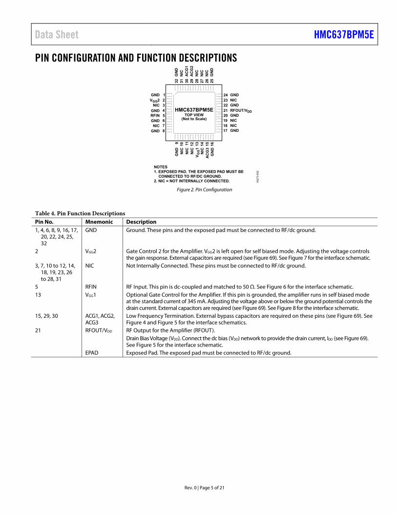
PIN CONFIGURATION AND FUNCTION DESCRIPTIONS
17
1
34
2
9
GNDVGG2
NICGND
56
RFINGND
7NIC8GND GND
18 NIC19 NIC20 GND21 RFOUT/VDD
22 GND23 NIC24 GND
NOTES1. EXPOSED PAD. THE EXPOSED PAD MUST BE CONNECTED TO RF/DC GROUND.2. NIC = NOT INTERNALLY CONNECTED.
GN
D
12N
IC11
NIC
10N
IC
13V G
G1
14N
IC15
AC
G3
16G
ND
25G
ND
26N
IC27
NIC
28N
IC29
AC
G2
30A
CG
131
NIC
32G
ND
HMC637BPM5ETOP VIEW
(Not to Scale)
1627
3-00
2
Figure 2. Pin Configuration
Table 4. Pin Function Descriptions Pin No. Mnemonic Description 1, 4, 6, 8, 9, 16, 17,
20, 22, 24, 25, 32
GND Ground. These pins and the exposed pad must be connected to RF/dc ground.
2 VGG2 Gate Control 2 for the Amplifier. VGG2 is left open for self biased mode. Adjusting the voltage controls the gain response. External capacitors are required (see Figure 69). See Figure 7 for the interface schematic.
3, 7, 10 to 12, 14, 18, 19, 23, 26 to 28, 31
NIC Not Internally Connected. These pins must be connected to RF/dc ground.
5 RFIN RF Input. This pin is dc-coupled and matched to 50 Ω. See Figure 6 for the interface schematic. 13 VGG1 Optional Gate Control for the Amplifier. If this pin is grounded, the amplifier runs in self biased mode
at the standard current of 345 mA. Adjusting the voltage above or below the ground potential controls the drain current. External capacitors are required (see Figure 69). See Figure 8 for the interface schematic.
15, 29, 30 ACG1, ACG2, ACG3
Low Frequency Termination. External bypass capacitors are required on these pins (see Figure 69). See Figure 4 and Figure 5 for the interface schematics.
21 RFOUT/VDD RF Output for the Amplifier (RFOUT). Drain Bias Voltage (VDD). Connect the dc bias (VDD) network to provide the drain current, IDD (see Figure 69).
See Figure 5 for the interface schematic. EPAD Exposed Pad. The exposed pad must be connected to RF/dc ground.
HMC637BPM5E Data Sheet
Rev. 0 | Page 6 of 21
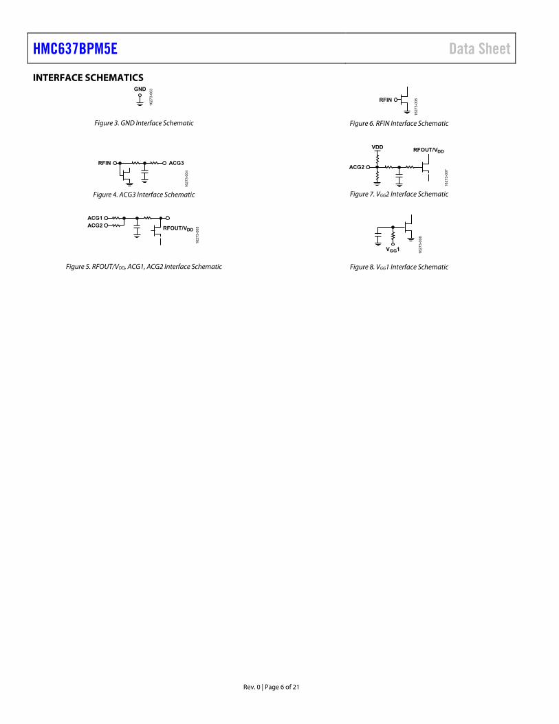
INTERFACE SCHEMATICS GND
1627
3-00
3
Figure 3. GND Interface Schematic
RFIN ACG3
1627
3-00
4
Figure 4. ACG3 Interface Schematic
ACG1
RFOUT/VDDACG2
1627
3-00
5
Figure 5. RFOUT/VDD, ACG1, ACG2 Interface Schematic
1627
3-00
6RFIN
Figure 6. RFIN Interface Schematic
ACG2
VDD RFOUT/VDD
1627
3-00
7
Figure 7. VGG2 Interface Schematic
VGG1
1627
3-00
8
Figure 8. VGG1 Interface Schematic

Data Sheet HMC637BPM5E
Rev. 0 | Page 7 of 21
TYPICAL PERFORMANCE CHARACTERISTIC
–25
–20
–15
–10
–5
0
5
10
15
20
0 1 2 3 4 5 6 7 8 9 10
RES
PON
SE (d
B)
FREQUENCY (GHz)
S11S21S22
1627
3-00
9
Figure 9. Gain and Return Loss Response vs. Frequency, Self Biased Mode, VDD = 12 V, VGG1 = GND, VGG2 = Open
8
9
10
11
12
13
14
15
16
17
18
0 1 2 3 4 5 6 7 8
GA
IN (d
B)
FREQUENCY (GHz)
8V9V10V11V12V13V
1627
3-01
0
Figure 10. Gain vs. Frequency for Various Supply Voltages (VDD), Self Biased
Mode, VGG1 = GND, VGG2 = Open
8
9
10
11
12
13
14
15
16
17
18
0 1 2 3 4 5 6 7 8
GA
IN (d
B)
FREQUENCY (GHz)
4V5V (SELF BIASED)6V
1627
3-01
1
Figure 11. Gain vs. Frequency for Various VGG2 Values, VDD = 12 V, VGG1 = GND
8
9
10
11
12
13
14
15
16
17
18
0 1 2 3 4 5 6 7 8
GA
IN (d
B)
FREQUENCY (GHz)
–55°C+25°C+85°C
1627
3-01
2
Figure 12. Gain vs. Frequency for Various Temperatures, Self Biased Mode, VDD = 12 V, VGG1 = GND, VGG2 = Open
8
9
10
11
12
13
14
15
16
17
18
0 1 2 3 4 5 6 7 8
GA
IN (d
B)
FREQUENCY (GHz)
345mA (SELF BIASED)250mA300mA350mA400mA450mA
1627
3-01
3
Figure 13. Gain vs. Frequency for Various Supply Currents (IDD), Externally
Biased Mode, VDD = 12 V, VGG2 = Open, Controlled VGG1
–20
–15
–10
–5
0
0 1 2 3 4 5 6 7 8
RET
UR
N L
OSS
(dB
)
FREQUENCY (GHz)
–55°C+25°C+85°C
1627
3-01
4
Figure 14. Input Return Loss vs. Frequency for Various Temperatures, Self Biased Mode, VDD = 12 V, VGG1 = GND, VGG2 = Open
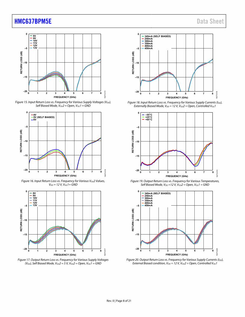
HMC637BPM5E Data Sheet
Rev. 0 | Page 8 of 21
–20
–15
–10
–5
0
0 1 2 3 4 5 6 7 8
RET
UR
N L
OSS
(dB
)
FREQUENCY (GHz)
8V9V10V11V12V13V
1627
3-01
5
Figure 15. Input Return Loss vs. Frequency for Various Supply Voltages (VDD),
Self Biased Mode, VGG2 = Open, VGG1 = GND
–20
–15
–10
–5
0
0 1 2 3 4 5 6 7 8
RET
UR
N L
OSS
(dB
)
FREQUENCY (GHz)
4V5V (SELF BIASED)6V
1627
3-01
6
Figure 16. Input Return Loss vs. Frequency for Various VGG2 Values,
VDD = 12 V, VGG1= GND
–20
–15
–10
–5
0
0 1 2 3 4 5 6 7 8
RET
UR
N L
OSS
(dB
)
FREQUENCY (GHz)
8V9V10V11V12V13V
1627
3-01
7
Figure 17. Output Return Loss vs. Frequency for Various Supply Voltages
(VDD), Self Biased Mode, VGG2 = 5 V, VGG2 = Open, VGG1 = GND
–20
–15
–10
–5
0
0 1 2 3 4 5 6 7 8
RET
UR
N L
OSS
(dB
)
FREQUENCY (GHz)
345mA (SELF BIASED)250mA300mA350mA400mA450mA
1627
3-01
8
Figure 18. Input Return Loss vs. Frequency for Various Supply Currents (IDD),
Externally Biased Mode, VDD = 12 V, VGG2 = Open, Controlled VGG1
–20
–15
–10
–5
0
0 1 2 3 4 5 6 7 8
RET
UR
N L
OSS
(dB
)
FREQUENCY (GHz)
–55°C+25°C+85°C
1627
3-01
9
Figure 19. Output Return Loss vs. Frequency for Various Temperatures,
Self Biased Mode, VDD =12 V, VGG2 = Open, VGG1 = GND
–20
–15
–10
–5
0
0 1 2 3 4 5 6 7 8
RET
UR
N L
OSS
(dB
)
FREQUENCY (GHz)
345mA (SELF BIASED)250mA300mA350mA400mA450mA
1627
3-02
0
Figure 20. Output Return Loss vs. Frequency for Various Supply Currents (IDD),
External Biased condition, VDD = 12 V, VGG2 = Open, Controlled VGG1
Data Sheet HMC637BPM5E
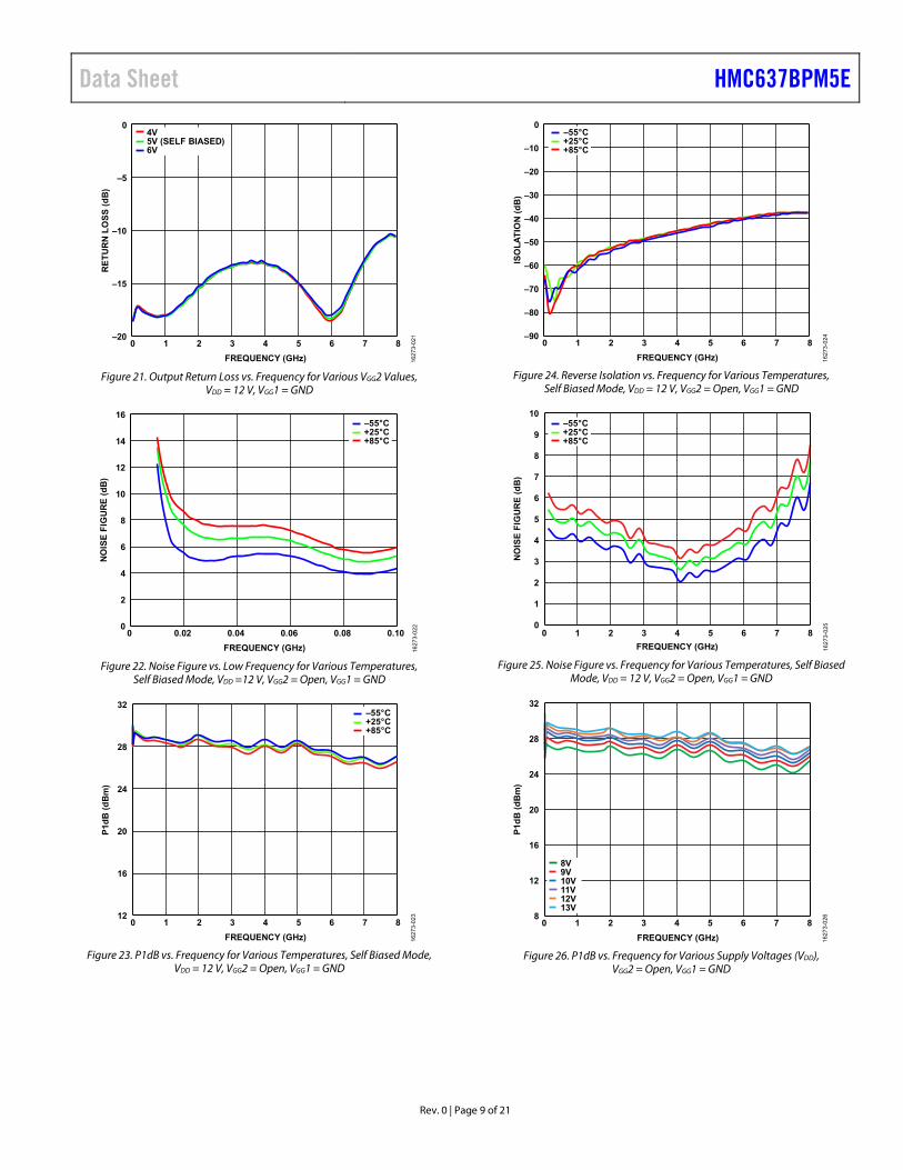
Rev. 0 | Page 9 of 21
FREQUENCY (GHz)
–20
–15
–10
–5
0
0 1 2 3 4 5 6 7 8
RET
UR
N L
OSS
(dB
)
4V5V (SELF BIASED)6V
1627
3-02
1
Figure 21. Output Return Loss vs. Frequency for Various VGG2 Values,
VDD = 12 V, VGG1 = GND
0
2
4
6
8
10
12
14
16
0 0.02 0.04 0.06 0.08 0.10
NO
ISE
FIG
UR
E (d
B)
FREQUENCY (GHz)
–55°C+25°C+85°C
1627
3-02
2
Figure 22. Noise Figure vs. Low Frequency for Various Temperatures,
Self Biased Mode, VDD =12 V, VGG2 = Open, VGG1 = GND
12
16
20
24
28
32
0 1 2 3 4 5 6 7 8
P1dB
(dB
m)
FREQUENCY (GHz)
–55°C+25°C+85°C
1627
3-02
3
Figure 23. P1dB vs. Frequency for Various Temperatures, Self Biased Mode,
VDD = 12 V, VGG2 = Open, VGG1 = GND
–90
–80
–70
–60
–50
–40
–30
–20
–10
0
0 1 2 3 4 5 6 7 8
ISO
LATI
ON
(dB
)
FREQUENCY (GHz) 1627
3-02
4
–55°C+25°C+85°C
Figure 24. Reverse Isolation vs. Frequency for Various Temperatures,
Self Biased Mode, VDD = 12 V, VGG2 = Open, VGG1 = GND
0
1
2
3
4
5
6
7
8
9
10
0 1 2 3 4 5 6 7 8
NO
ISE
FIG
UR
E (d
B)
FREQUENCY (GHz)
–55°C+25°C+85°C
1627
3-02
5
Figure 25. Noise Figure vs. Frequency for Various Temperatures, Self Biased
Mode, VDD = 12 V, VGG2 = Open, VGG1 = GND
8
12
16
20
24
28
32
0 1 2 3 4 5 6 7 8
P1dB
(dB
m)
FREQUENCY (GHz)
8V9V10V11V12V13V
1627
3-02
6
Figure 26. P1dB vs. Frequency for Various Supply Voltages (VDD),
VGG2 = Open, VGG1 = GND
HMC637BPM5E Data Sheet
Rev. 0 | Page 10 of 21
8
12
16
20
24
28
32
0 1 2 3 4 5 6 7 8
P1dB
(dB
m)
FREQUENCY (GHz)
345mA (SELF BIASED)250mA300mA350mA400mA450mA
1627
3-02
7
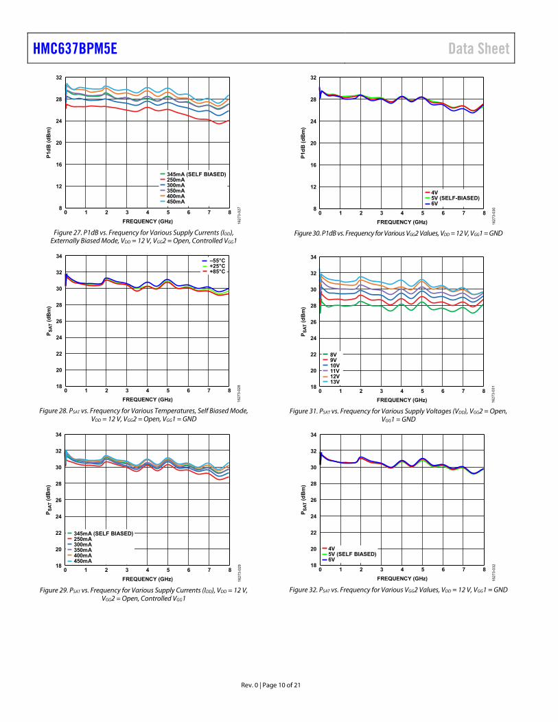
Figure 27. P1dB vs. Frequency for Various Supply Currents (IDD),
Externally Biased Mode, VDD = 12 V, VGG2 = Open, Controlled VGG1
18
20
22
24
26
28
30
32
34
0 1 2 3 4 5 6 7 8
P SAT
(dB
m)
FREQUENCY (GHz)
–55°C+25°C+85°C
1627
3-02
8
Figure 28. PSAT vs. Frequency for Various Temperatures, Self Biased Mode, VDD = 12 V, VGG2 = Open, VGG1 = GND
18
20
22
24
26
28
30
32
34
0 1 2 3 4 5 6 7 8
P SAT
(dB
m)
FREQUENCY (GHz)
345mA (SELF BIASED)250mA300mA350mA400mA450mA
1627
3-02
9
Figure 29. PSAT vs. Frequency for Various Supply Currents (IDD), VDD = 12 V,
VGG2 = Open, Controlled VGG1
8
12
16
20
24
28
32
0 1 2 3 4 5 6 7 8
P1dB
(dB
m)
FREQUENCY (GHz)
4V5V (SELF-BIASED)6V
1627
3-03
0
Figure 30. P1dB vs. Frequency for Various VGG2 Values, VDD = 12 V, VGG1 = GND
18
20
22
24
26
28
30
32
34
0 1 2 3 4 5 6 7 8
P SAT
(dB
m)
FREQUENCY (GHz)
8V9V10V11V12V13V
1627
3-03
1
Figure 31. PSAT vs. Frequency for Various Supply Voltages (VDD), VGG2 = Open,
VGG1 = GND
18
20
22
24
26
28
30
32
34
0 1 2 3 4 5 6 7 8
P SAT
(dB
m)
FREQUENCY (GHz)
4V5V (SELF BIASED)6V
1627
3-03
2
Figure 32. PSAT vs. Frequency for Various VGG2 Values, VDD = 12 V, VGG1 = GND

Data Sheet HMC637BPM5E
Rev. 0 | Page 11 of 21
0
5
10
15
20
25
30
0 1 2 3 4 5 6 7 8
PAE
(%)
FREQUENCY (GHz)
–55°C+25°C+85°C
1627
3-03
3
Figure 33. Power Added Efficiency (PAE) vs. Frequency for Various Temperatures,
Self Biased Mode, VDD = 12 V, VGG2 = Open, VGG1 = GND, PAE Measured at PSAT
0
5
10
15
20
25
30
0 1 2 3 4 5 6 7 8
PAE
(%)
FREQUENCY (GHz)
345mA (SELF BIASED)250mA300mA350mA400mA450mA
1627
3-03
4
Figure 34. PAE vs. Frequency for Various Supply Currents (IDD),
VDD = 12 V, VGG2 = Open, Controlled VGG1, PAE Measured at PSAT
330
345
360
375
390
405
420
435
0
5
10
15
20
25
30
35
0 2 4 6 8 10 12 14 16 18 20
I DD
(mA
)
P OU
T (d
Bm
), G
AIN
(dB
),PA
E (%
)
INPUT POWER (dBm)
POUTGAINPAEIDD
1627
3-03
5
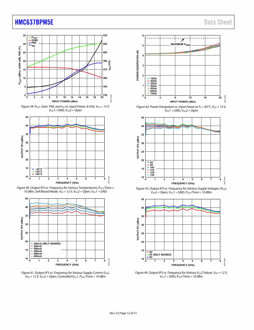
Figure 35. POUT, Gain, PAE, and IDD vs. Input Power, 1 GHz, VDD = 12 V,
VGG1= GND, VGG2 = Open
0
5
10
15
20
25
30
0 1 2 3 4 5 6 7 8
PAE
(%)
FREQUENCY (GHz)
8V9V10V11V12V13V
1627
3-03
6
Figure 36. PAE vs. Frequency for Various Supply Voltages (VDD),
VGG2 = Open, VGG1 = GND, PAE Measured at PSAT
0
5
10
15
20
25
30
0 1 2 3 4 5 6 7 8
PAE
(%)
FREQUENCY (GHz)
4V5V (SELF BIASED)6V
1627
3-03
7
Figure 37. PAE vs. Frequency for Various VGG2 Values, VDD =12 V,
VGG1 = GND, PAE Measured at PSAT
330
345
360
375
390
405
420
435
0
5
10
15
20
25
30
35
0 2 4 6 8 10 12 14 16 18 20
I DD
(mA
)
P OU
T (d
Bm
), G
AIN
(dB
),PA
E (%
)
INPUT POWER (dBm)
POUTGAINPAEIDD
1627
3-03
8
Figure 38. POUT, Gain, PAE, and IDD vs. Input Power, 3 GHz, VDD = 12 V, VGG1 = GND, VGG2 = Open
HMC637BPM5E Data Sheet
Rev. 0 | Page 12 of 21
0
5
10
15
20
25
30
35
0 2 4 6 8 10 12 14 16 18 20
P OU
T (d
Bm
), G
AIN
(dB
),PA
E (%
)
INPUT POWER (dBm)
330
345
360
375
390
405
420
435
I DD
(mA
)
POUTGAINPAEIDD
1627
3-03
9
Figure 39. POUT, Gain, PAE, and IDD vs. Input Power, 6 GHz, VDD = 12 V, VGG1= GND, VGG2 = Open
10
15
20
25
30
35
40
45
0 1 2 3 4 5 6 7 8
OU
TPU
T IP
3 (d
Bm
)
FREQUENCY (GHz)
–55°C+25°C+85°C
1627
3-04
0
Figure 40. Output IP3 vs. Frequency for Various Temperatures, POUT/Tone = 10 dBm, Self Biased Mode, VDD = 12 V, VGG2 = Open, VGG1 = GND
10
15
20
25
30
35
40
45
0 1 2 3 4 5 6 7 8
OU
TPU
T IP
3 (d
Bm
)
FREQUENCY (GHz)
345mA (SELF BIASED)250mA300mA350mA400mA450mA
1627
3-04
1
Figure 41. Output IP3 vs. Frequency for Various Supply Current (IDD), VDD = 12 V, VGG2 = Open, Controlled VGG1, POUT/Tone = 10 dBm
0
1
2
3
4
5
6
0 4 8 12 16 20
POW
ER D
ISSI
PATI
ON
(W)
INPUT POWER (dBm)
1GHz2GHz3GHz4GHz5GHz6GHz7GHz
1627
3-04
2
MAXIMUM PDISS
Figure 42. Power Dissipation vs. Input Power at TA = 85°C, VDD = 12 V, VGG1 = GND, VGG2 = Open
10
15
20
25
30
35
40
45
0 1 2 3 4 5 6 7 8
OU
TPU
T IP
3 (d
Bm
)
FREQUENCY (GHz)
8V9V10V11V12V13V
1627
3-04
3
Figure 43. Output IP3 vs. Frequency for Various Supply Voltages (VDD), VGG2 = Open, VGG1 = GND, POUT/Tone = 10 dBm
10
15
20
25
30
35
40
45
0 1 2 3 4 5 6 7 8
OU
TPU
T IP
3 (d
Bm
)
FREQUENCY (GHz)
4V5V (SELF BIASED)6V
1627
3-04
4
Figure 44. Output IP3 vs. Frequency for Various VGG2 Values, VDD = 12 V, VGG1 = GND, POUT/Tone = 10 dBm
Data Sheet HMC637BPM5E
Rev. 0 | Page 13 of 21
10
15
20
25
30
35
40
45
0 1 2 3 4 5 6 7 8
OU
TPU
T IP
3 (d
Bm
)
FREQUENCY (GHz)
0dBm10dBm20dBm
1627
3-04
5
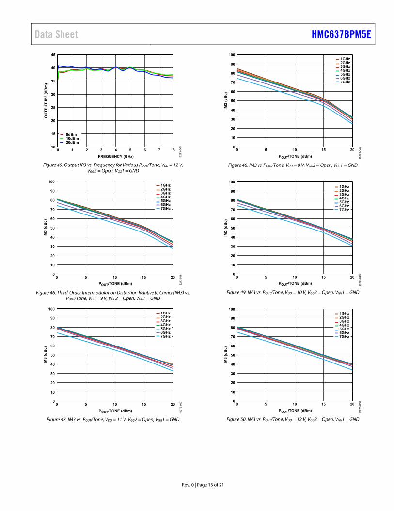
Figure 45. Output IP3 vs. Frequency for Various POUT/Tone, VDD = 12 V,
VGG2 = Open, VGG1 = GND
0
10
20
30
40
50
60
70
80
90
100
0 5 10 15 20
IM3
(dB
c)
POUT/TONE (dBm)
1GHz2GHz3GHz4GHz5GHz6GHz7GHz
1627
3-04
6
Figure 46. Third-Order Intermodulation Distortion Relative to Carrier (IM3) vs.
POUT/Tone, VDD = 9 V, VGG2 = Open, VGG1 = GND
0
10
20
30
40
50
60
70
80
90
100
0 5 10 15 20
IM3
(dB
c)
POUT/TONE (dBm)
1GHz2GHz3GHz4GHz5GHz6GHz7GHz
1627
3-04
7
Figure 47. IM3 vs. POUT/Tone, VDD = 11 V, VGG2 = Open, VGG1 = GND
POUT/TONE (dBm)
0
10
20
30
40
50
60
70
80
90
100
0 5 10 15 20
IM3
(dB
c)
1GHz2GHz3GHz4GHz5GHz6GHz7GHz
1627
3-04
8
Figure 48. IM3 vs. POUT/Tone, VDD = 8 V, VGG2 = Open, VGG1 = GND
POUT/TONE (dBm)
0
10
20
30
40
50
60
70
80
90
100
0 5 10 15 20
IM3
(dB
c)
1GHz2GHz3GHz4GHz5GHz6GHz7GHz
1627
3-04
9
Figure 49. IM3 vs. POUT/Tone, VDD = 10 V, VGG2 = Open, VGG1 = GND
0
10
20
30
40
50
60
70
80
90
100
0 5 10 15 20
IM3
(dB
c)
POUT/TONE (dBm)
1GHz2GHz3GHz4GHz5GHz6GHz7GHz
1627
3-05
0
Figure 50. IM3 vs. POUT/Tone, VDD = 12 V, VGG2 = Open, VGG1 = GND

HMC637BPM5E Data Sheet
Rev. 0 | Page 14 of 21
0
10
20
30
40
50
60
70
80
90
100
0 5 10 15 20
IM3
(dB
c)
POUT/TONE (dBm)
1627
3-05
1
1GHz2GHz3GHz4GHz5GHz6GHz7GHz
Figure 51. IM3 vs. POUT/Tone, VDD = 13 V, VGG2 = Open, VGG1 = GND
0
10
20
30
40
50
60
0 1 2 3 4 5 6 7 8
OU
TPU
T IP
2 (d
Bm
)
FREQUENCY (GHz)
8V9V10V11V12V13V
1627
3-05
2
Figure 52. Output IP2 vs. Frequency for Various Supply Voltages (VDD),
VGG2 = Open, VGG1 = GND, POUT/Tone = 10 dBm
10
15
20
25
30
35
40
45
50
55
60
0 1 2 3 4 5 6 7 8
OU
TPU
T IP
2 (d
Bm
)
FREQUENCY (GHz)
4V5V (SELF BIASED)6V
1627
3-05
3
Figure 53. Output IP2 vs. Frequency for Various VGG2 Values, VDD =12 V,
VGG1 = GND, POUT/Tone = 10 dBm
0
10
20
30
40
50
60
0 1 2 3 4 5 6 7 8
OU
TPU
T IP
2 (d
Bm
)
FREQUENCY (GHz)
–55°C+25°C+85°C
1627
3-05
4
Figure 54. Output IP2 vs. Frequency for Various Temperatures, POUT/Tone =
10 dBm, VDD =12 V, VGG2 = Open, VGG1 = GND (Self Biased)
0
10
20
30
40
50
60
70
0 1 2 3 4 5 6 7 8
OU
TPU
T IP
2 (d
Bm
)
FREQUENCY (GHz)
345mA (SELF BIASED)250mA300mA350mA400mA450mA
1627
3-05
5
Figure 55. Output IP2 vs. Frequency for Various Supply Currents (IDD),
VDD = 12 V, VGG2 = Open, Controlled VGG1, POUT/Tone = 10 dBm
0
10
20
30
40
50
60
0 1 2 3 4 5 6 7 8
OU
TPU
T IP
2 (d
Bm
)
FREQUENCY (GHz)
0dBm10dBm20dBm
1627
3-05
6
Figure 56. Output IP2 vs. Frequency for Various POUT/Tone Values, VDD = 12 V,
VGG2 = Open, VGG1 = GND
Data Sheet HMC637BPM5E
Rev. 0 | Page 15 of 21
0
10
20
30
40
50
60
1 2 3 4 5 6 7 8
SEC
ON
D H
AR
MO
NIC
(dB
c)
FREQUENCY (GHz)
–55°C+25°C+85°C
1627
3-05
7
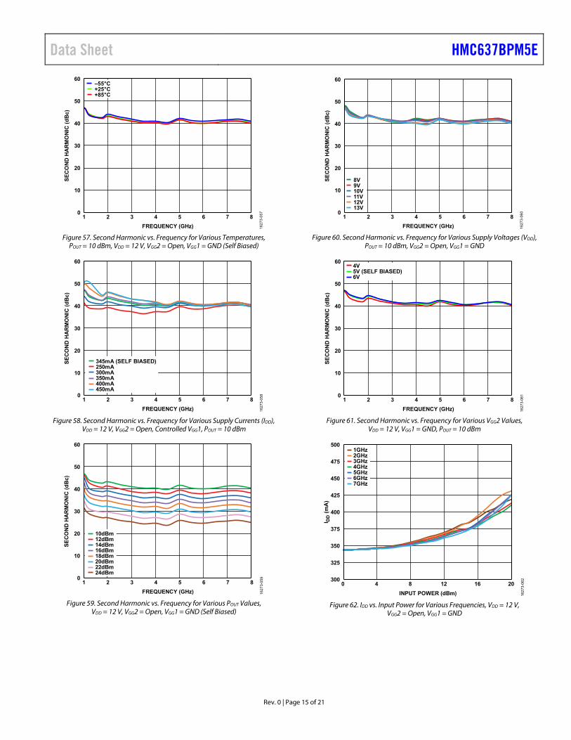
Figure 57. Second Harmonic vs. Frequency for Various Temperatures,
POUT = 10 dBm, VDD = 12 V, VGG2 = Open, VGG1 = GND (Self Biased)
0
10
20
30
40
50
60
1 2 3 4 5 6 7 8
SEC
ON
D H
AR
MO
NIC
(dB
c)
FREQUENCY (GHz)
345mA (SELF BIASED)250mA300mA350mA400mA450mA
1627
3-05
8
Figure 58. Second Harmonic vs. Frequency for Various Supply Currents (IDD),
VDD = 12 V, VGG2 = Open, Controlled VGG1, POUT = 10 dBm
0
10
20
30
40
50
60
1 2 3 4 5 6 7 8
SEC
ON
D H
AR
MO
NIC
(dB
c)
FREQUENCY (GHz)
10dBm12dBm14dBm16dBm18dBm20dBm22dBm24dBm
1627
3-05
9
Figure 59. Second Harmonic vs. Frequency for Various POUT Values,
VDD = 12 V, VGG2 = Open, VGG1 = GND (Self Biased)
0
10
20
30
40
50
60
1 2 3 4 5 6 7 8
SEC
ON
D H
AR
MO
NIC
(dB
c)
FREQUENCY (GHz)
8V9V10V11V12V13V
1627
3-06
0
Figure 60. Second Harmonic vs. Frequency for Various Supply Voltages (VDD),
POUT = 10 dBm, VGG2 = Open, VGG1 = GND
0
10
20
30
40
50
60
1 2 3 4 5 6 7 8
SEC
ON
D H
AR
MO
NIC
(dB
c)
FREQUENCY (GHz)
4V5V (SELF BIASED)6V
1627
3-06
1
Figure 61. Second Harmonic vs. Frequency for Various VGG2 Values,
VDD = 12 V, VGG1 = GND, POUT = 10 dBm
300
325
350
375
400
425
450
475
500
0 4 8 12 16 20
I DD
(mA
)
INPUT POWER (dBm)
1GHz2GHz3GHz4GHz5GHz6GHz7GHz
1627
3-06
2
Figure 62. IDD vs. Input Power for Various Frequencies, VDD = 12 V,
VGG2 = Open, VGG1 = GND
HMC637BPM5E Data Sheet
Rev. 0 | Page 16 of 21
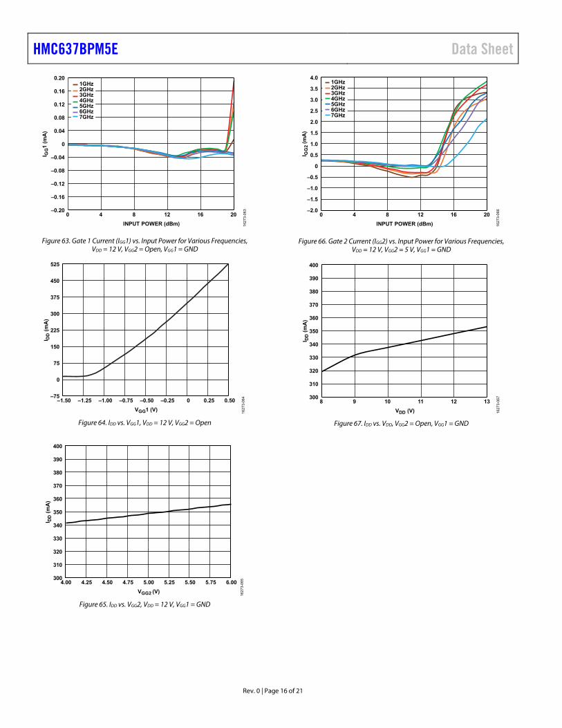
–0.20
–0.16
–0.12
–0.08
–0.04
0
0.04
0.08
0.12
0.16
0.20
0 4 8 12 16 20
I GG
1 (m
A)
INPUT POWER (dBm)
1GHz2GHz3GHz4GHz5GHz6GHz7GHz
1627
3-06
3
Figure 63. Gate 1 Current (IGG1) vs. Input Power for Various Frequencies, VDD = 12 V, VGG2 = Open, VGG1 = GND
–75
0
75
150
225
300
375
450
525
–1.50 –1.25 –1.00 –0.75 –0.50 –0.25 0 0.25 0.50
I DD
(mA
)
VGG1 (V)
1627
3-06
4
Figure 64. IDD vs. VGG1, VDD = 12 V, VGG2 = Open
1627
3-06
5300
310
320
330
340
350
360
370
380
390
400
4.00 4.25 4.50 4.75 5.00 5.25 5.50 5.75 6.00
I DD
(mA
)
VGG2 (V)
Figure 65. IDD vs. VGG2, VDD = 12 V, VGG1 = GND
–2.0
–1.5
–1.0
–0.5
0
0.5
1.0
1.5
2.0
2.5
3.0
3.5
4.0
0 4 8 12 16 20
I GG
2 (m
A)
INPUT POWER (dBm)
1GHz2GHz3GHz4GHz5GHz6GHz7GHz
1627
3-06
6
Figure 66. Gate 2 Current (IGG2) vs. Input Power for Various Frequencies, VDD = 12 V, VGG2 = 5 V, VGG1 = GND
300
310
320
330
340
350
360
370
380
390
400
8 9 10 11 12 13
I DD
(mA
)
VDD (V) 1627
3-06
7
Figure 67. IDD vs. VDD, VGG2 = Open, VGG1 = GND
Data Sheet HMC637BPM5E
Rev. 0 | Page 17 of 21
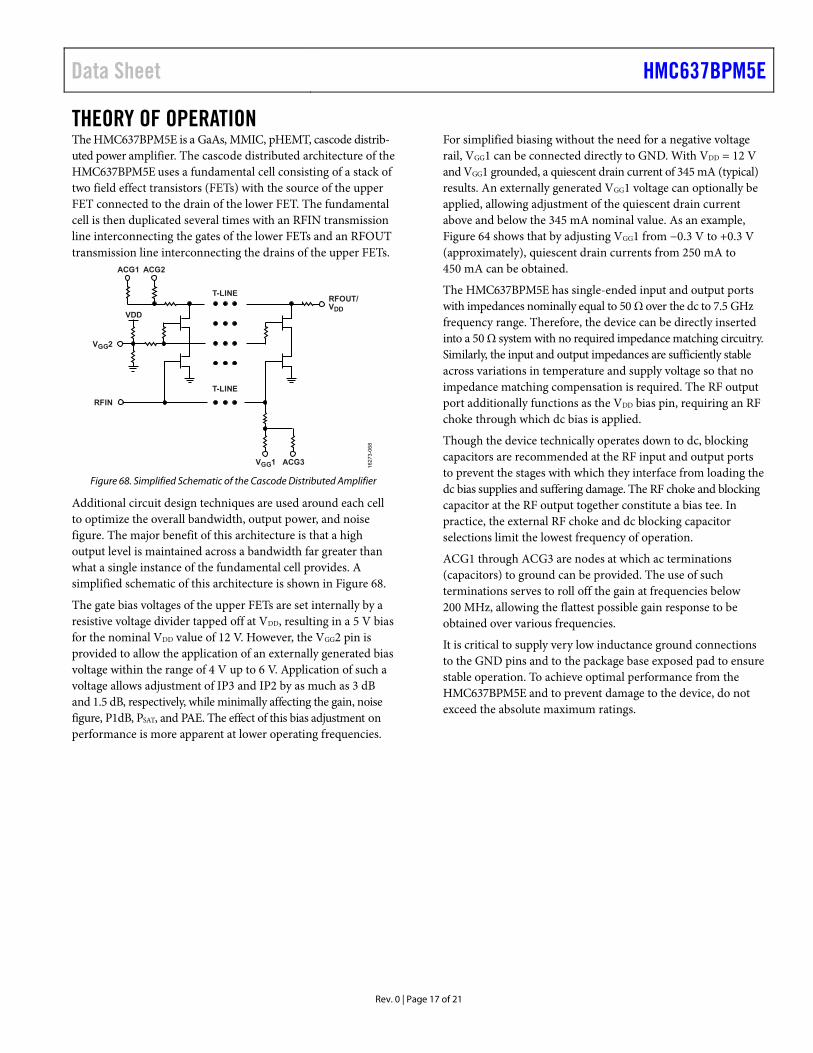
THEORY OF OPERATION The HMC637BPM5E is a GaAs, MMIC, pHEMT, cascode distrib-uted power amplifier. The cascode distributed architecture of the HMC637BPM5E uses a fundamental cell consisting of a stack of two field effect transistors (FETs) with the source of the upper FET connected to the drain of the lower FET. The fundamental cell is then duplicated several times with an RFIN transmission line interconnecting the gates of the lower FETs and an RFOUT transmission line interconnecting the drains of the upper FETs.
ACG2
T-LINE
T-LINE
RFOUT/VDD
ACG1
ACG3VGG1
VGG2
RFIN
VDD
1627
3-06
8
Figure 68. Simplified Schematic of the Cascode Distributed Amplifier
Additional circuit design techniques are used around each cell to optimize the overall bandwidth, output power, and noise figure. The major benefit of this architecture is that a high output level is maintained across a bandwidth far greater than what a single instance of the fundamental cell provides. A simplified schematic of this architecture is shown in Figure 68.
The gate bias voltages of the upper FETs are set internally by a resistive voltage divider tapped off at VDD, resulting in a 5 V bias for the nominal VDD value of 12 V. However, the VGG2 pin is provided to allow the application of an externally generated bias voltage within the range of 4 V up to 6 V. Application of such a voltage allows adjustment of IP3 and IP2 by as much as 3 dB and 1.5 dB, respectively, while minimally affecting the gain, noise figure, P1dB, PSAT, and PAE. The effect of this bias adjustment on performance is more apparent at lower operating frequencies.
For simplified biasing without the need for a negative voltage rail, VGG1 can be connected directly to GND. With VDD = 12 V and VGG1 grounded, a quiescent drain current of 345 mA (typical) results. An externally generated VGG1 voltage can optionally be applied, allowing adjustment of the quiescent drain current above and below the 345 mA nominal value. As an example, Figure 64 shows that by adjusting VGG1 from −0.3 V to +0.3 V (approximately), quiescent drain currents from 250 mA to 450 mA can be obtained.
The HMC637BPM5E has single-ended input and output ports with impedances nominally equal to 50 Ω over the dc to 7.5 GHz frequency range. Therefore, the device can be directly inserted into a 50 Ω system with no required impedance matching circuitry. Similarly, the input and output impedances are sufficiently stable across variations in temperature and supply voltage so that no impedance matching compensation is required. The RF output port additionally functions as the VDD bias pin, requiring an RF choke through which dc bias is applied.
Though the device technically operates down to dc, blocking capacitors are recommended at the RF input and output ports to prevent the stages with which they interface from loading the dc bias supplies and suffering damage. The RF choke and blocking capacitor at the RF output together constitute a bias tee. In practice, the external RF choke and dc blocking capacitor selections limit the lowest frequency of operation.
ACG1 through ACG3 are nodes at which ac terminations (capacitors) to ground can be provided. The use of such terminations serves to roll off the gain at frequencies below 200 MHz, allowing the flattest possible gain response to be obtained over various frequencies.
It is critical to supply very low inductance ground connections to the GND pins and to the package base exposed pad to ensure stable operation. To achieve optimal performance from the HMC637BPM5E and to prevent damage to the device, do not exceed the absolute maximum ratings.
HMC637BPM5E Data Sheet
Rev. 0 | Page 18 of 21
APPLICATIONS INFORMATION Capacitive bypassing is required for VDD and VGG1, as shown in the typical application circuit in Figure 69. Both the RFIN and RFOUT/VDD pins are dc-coupled. Use of an external dc blocking capacitor at RFIN is recommended. Use of an external RF choke plus a dc blocking capacitor (for example, a bias tee) at RFOUT/ VDD is required. For wideband applications, ensure that the frequency responses of the external biasing and blocking components are adequate for use across the entire frequency range of the application.
The HMC637BPM5E operates in either self biased or externally biased mode. To operate in self biased mode, ground the VGG1 pin and leave VGG2 open. For the externally biased configuration, adjust VGG1 within −2 V to +0.5 V to set the target drain current and adjust VGG2 from 4 V to 6 V for IP2 and IP3 control.
The recommended bias sequence during power-up for self biased operation is as follows:
1. Connect GND. 2. Set VDD to 12 V. 3. Apply the RF signal.
The recommended bias sequence during power-down for self biased operation is as follows :
1. Turn off the RFIN signal. 2. Set VDD to 0 V.
The recommended bias sequence during power-up for externally biased operation is as follows:
1. Connect GND. 2. Set VGG1 to −2 V. 3. Set VDD to 12 V. 4. Increase VGG1 to achieve the desired quiescent current (IDQ). 5. Apply the RF signal. 6. When using the IP2/IP3 control function, apply a voltage
from 4 V to 6 V until the desired performance is obtained.
The recommended bias sequence during power-down for externally biased operation is as follows:
1. Turn off the RFIN signal. 2. Remove the VGG2 voltage. 3. Decrease VGG1 to −2 V to achieve a typical IDQ of 0 mA. 4. Set VDD to 0 V. 5. Set VGG1 to 0 V.
Adhere to the values shown in the Absolute Maximum Ratings section.
Unless otherwise noted, all measurements and data shown were taken using the typical application circuit (see Figure 69), and biased per the conditions in this section. The bias conditions described in this section are the operating points recommended to optimize the overall device performance. Operation using other bias conditions may result in performance that differs from what is shown in the Typical Performance Characteristic section. To obtain the best performance while avoiding damage to the device, follow the recommended biasing sequences described in this section.
Data Sheet HMC637BPM5E
Rev. 0 | Page 19 of 21
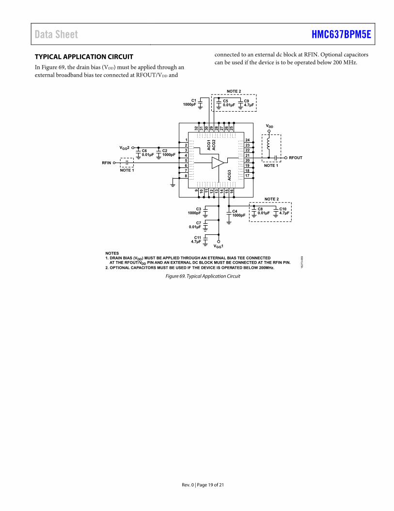
TYPICAL APPLICATION CIRCUIT In Figure 69, the drain bias (VDD) must be applied through an external broadband bias tee connected at RFOUT/VDD and
connected to an external dc block at RFIN. Optional capacitors can be used if the device is to be operated below 200 MHz.
17
1
34
2
9
VGG2
56RFIN
78
18192021 RFOUT
NOTE 1
NOTE 2
NOTE 1
NOTES1. DRAIN BIAS (VDD) MUST BE APPLIED THROUGH AN ETERNAL BIAS TEE CONNECTED
AT THE RFOUT/VDD PIN AND AN EXTERNAL DC BLOCK MUST BE CONNECTED AT THE RFIN PIN.2. OPTIONAL CAPACITORS MUST BE USED IF THE DEVICE IS OPERATED BELOW 200MHz.
C11000pF
C41000pF
C50.01µF
C21000pF
C60.01µF
C94.7µF
VDD
222324
121110 13
VGG1
14 15A
CG
316
2526272829A
CG
2
30A
CG
1
3132NOTE 2
C80.01µF
C104.7µF
C31000pF
C70.01µF
C114.7µF
1627
3-06
9
Figure 69. Typical Application Circuit
HMC637BPM5E Data Sheet
Rev. 0 | Page 20 of 21
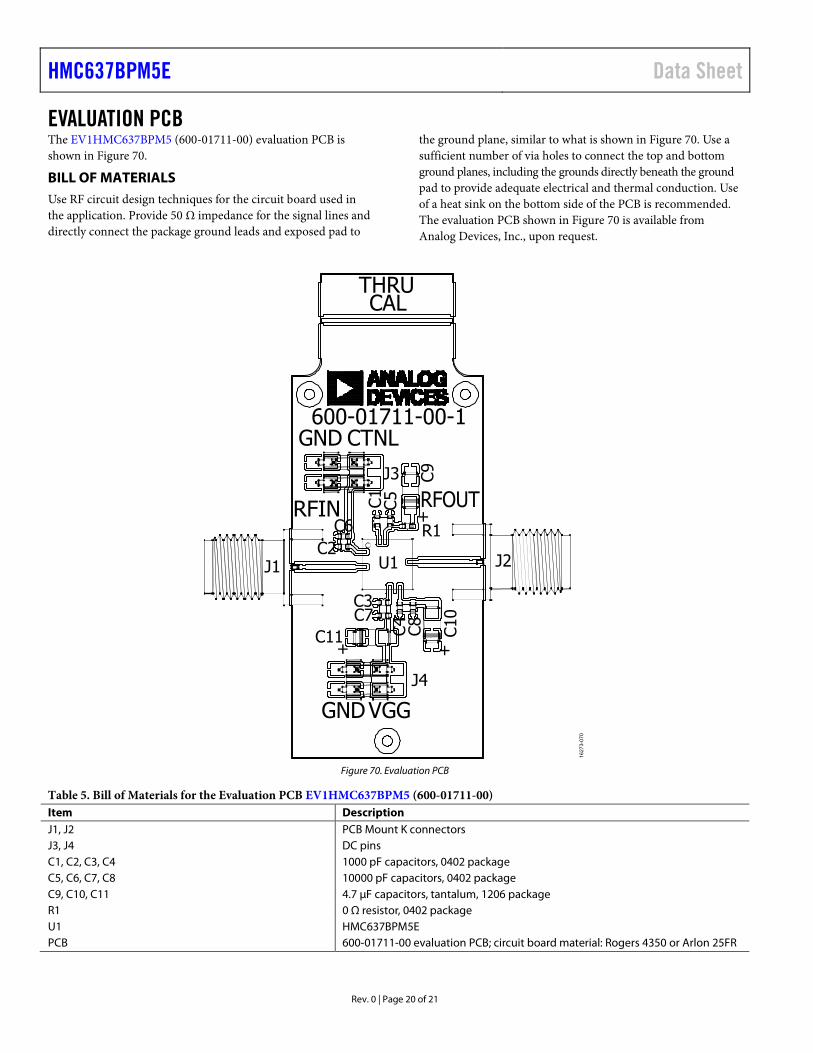
EVALUATION PCB The EV1HMC637BPM5 (600-01711-00) evaluation PCB is shown in Figure 70.
BILL OF MATERIALS Use RF circuit design techniques for the circuit board used in the application. Provide 50 Ω impedance for the signal lines and directly connect the package ground leads and exposed pad to
the ground plane, similar to what is shown in Figure 70. Use a sufficient number of via holes to connect the top and bottom ground planes, including the grounds directly beneath the ground pad to provide adequate electrical and thermal conduction. Use of a heat sink on the bottom side of the PCB is recommended. The evaluation PCB shown in Figure 70 is available from Analog Devices, Inc., upon request.
600-01711-00-1CTNLGND
VGG
RFIN RFOUT
THRUCAL
GND
C11 + C4
C2C6
C8
C3C7
C1
C10
+
+
C9
C5
J1 J2
R1
J3
J4
U116
273-
070
Figure 70. Evaluation PCB
Table 5. Bill of Materials for the Evaluation PCB EV1HMC637BPM5 (600-01711-00) Item Description J1, J2 PCB Mount K connectors J3, J4 DC pins C1, C2, C3, C4 1000 pF capacitors, 0402 package C5, C6, C7, C8 10000 pF capacitors, 0402 package C9, C10, C11 4.7 µF capacitors, tantalum, 1206 package R1 0 Ω resistor, 0402 package U1 HMC637BPM5E PCB 600-01711-00 evaluation PCB; circuit board material: Rogers 4350 or Arlon 25FR
Data Sheet HMC637BPM5E
Rev. 0 | Page 21 of 21
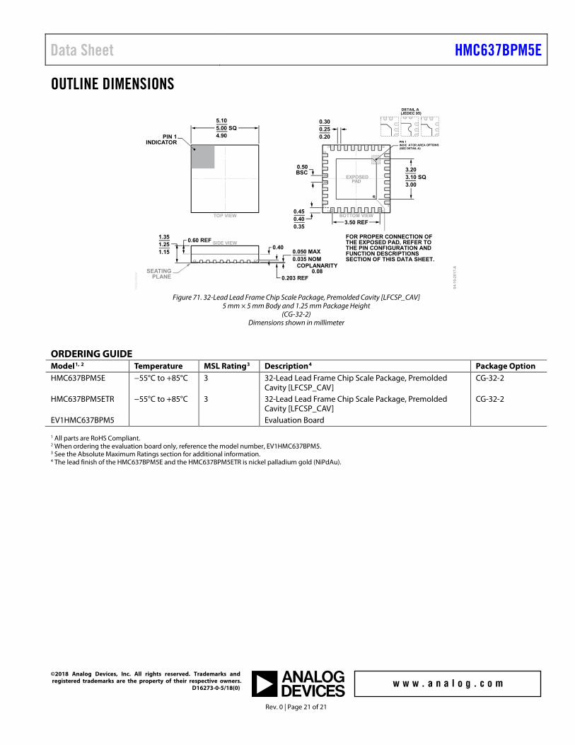
OUTLINE DIMENSIONS
04-1
9-20
17-A
1
0.50BSC
BOTTOM VIEWTOP VIEW
SIDE VIEW
PIN 1INDICATOR
32
916
17
24
25
8
0.300.250.20
5.105.00 SQ4.90
FOR PROPER CONNECTION OFTHE EXPOSED PAD, REFER TOTHE PIN CONFIGURATION ANDFUNCTION DESCRIPTIONSSECTION OF THIS DATA SHEET.
0.450.400.35
3.203.10 SQ3.00
PKG
-005
068
3.50 REF
EXPOSEDPAD
1.351.251.15 0.050 MAX
0.035 NOM
0.203 REF
0.400.60 REF
COPLANARITY0.08SEATING
PLANE
PIN 1INDIC ATOR AREA OPTIONS(SEE DETAIL A)
DETAIL A(JEDEC 95)
Figure 71. 32-Lead Lead Frame Chip Scale Package, Premolded Cavity [LFCSP_CAV]
5 mm × 5 mm Body and 1.25 mm Package Height (CG-32-2)
Dimensions shown in millimeter
ORDERING GUIDE Model1, 2 Temperature MSL Rating3 Description4 Package Option HMC637BPM5E −55°C to +85°C 3 32-Lead Lead Frame Chip Scale Package, Premolded
Cavity [LFCSP_CAV] CG-32-2
HMC637BPM5ETR −55°C to +85°C 3 32-Lead Lead Frame Chip Scale Package, Premolded Cavity [LFCSP_CAV]
CG-32-2
EV1HMC637BPM5 Evaluation Board 1 All parts are RoHS Compliant. 2 When ordering the evaluation board only, reference the model number, EV1HMC637BPM5. 3 See the Absolute Maximum Ratings section for additional information. 4 The lead finish of the HMC637BPM5E and the HMC637BPM5ETR is nickel palladium gold (NiPdAu).
©2018 Analog Devices, Inc. All rights reserved. Trademarks and registered trademarks are the property of their respective owners. D16273-0-5/18(0)


![F3JR MB R20 1211[31731]ncandelier.free.fr/asus/ASUS_F3JR_R20.pdfH_D#50 H_TMS H_TDO H_TCK H_TRST# H_PREQ# +VCCP +VCCP +VCCP +VCCP GND GND GND GND GND GND GND TPC26T 1 T1 R8 1 2 56Ohm](https://static.fdocuments.net/doc/165x107/5faf0ab01979a324157ec2b6/f3jr-mb-r20-121131731-hd50-htms-htdo-htck-htrst-hpreq-vccp-vccp-vccp.jpg)

![GENRAL WIRING (GENRAL WIRING-1) · sdcd vdd(3r3v) sddat0 sd board gnd gnd gnd 3r3v 3r3v gnd maindak maindbk 5v [main dial] pbabk gnd pbbbk pclek pbbak rfl 3r3v 3r3v gnd gnd afl phoe](https://static.fdocuments.net/doc/165x107/5c000ba809d3f2c9268ca1e5/genral-wiring-genral-wiring-1-sdcd-vdd3r3v-sddat0-sd-board-gnd-gnd-gnd-3r3v.jpg)