
GaAs-Based Semiconductor Optical Amplifiers with Quantum Dots ...
143
GaAs-Based Semiconductor Optical Amplifiers with Quantum Dots as an Active Medium vorgelegt von Diplom-Physiker Matthias Lämmlin aus Müllheim von der Fakultät II – Mathematik und Naturwissenschaften der Technischen Universität Berlin zur Erlangung des akademischen Grades Doktor der Naturwissenschaften – Dr. rer. nat. – genehmigte Dissertation Promotionsausschuss: Vorsitzender: Prof. Dr. E. Schöll Berichter / Gutachter: Prof. Dr. D. Bimberg Berichter / Gutachter: Prof. Dr. N. N. Ledentsov Tag der wissenschaftlichen Aussprache: 21.12.2006 Berlin 2007 D 83
Transcript of GaAs-Based Semiconductor Optical Amplifiers with Quantum Dots ...
GaAs-Based Semiconductor Optical Amplifiers
with Quantum Dots as an Active Medium
vorgelegt von
Diplom-Physiker
Matthias Lämmlin
aus Müllheim
von der Fakultät II – Mathematik und Naturwissenschaften der Technischen Universität Berlin
zur Erlangung des akademischen Grades
Doktor der Naturwissenschaften – Dr. rer. nat. –
genehmigte Dissertation
Promotionsausschuss: Vorsitzender: Prof. Dr. E. Schöll Berichter / Gutachter: Prof. Dr. D. Bimberg Berichter / Gutachter: Prof. Dr. N. N. Ledentsov Tag der wissenschaftlichen Aussprache: 21.12.2006
Berlin 2007
D 83

Zusammenfassung
In dieser Arbeit über GaAs-basierte optische Halbleiterverstärker (SOA) mit InGaAs Quantenpunkten (QPen) als aktivem Material wird über die Herstellung und Charakterisierung solcher Bauelemente für optische Verstärkung im 1.3 µm Wellenlängenbereich berichtet.
Ein Teil der Arbeit befasst sich mit der Simulation und Modellierung der Verstärker, in der zentrale Bauelementeeigenschaften untersucht werden, die für das Design von schrägen Wellenleitern und Anti-Reflektionsbeschichtungen wichtig sind und die Aufschluss über das generelle Gewinn- und Sättigungsverhalten von Verstärkern geben. Dieser theoretische Teil der Arbeit beschäftigt sich mit den besonderen Eigenschaften (p-Dotierung, Alphafaktor, inhomogene Verbreiterung, Sättigungs- und Gewinnerholungsmechanismen) von QPen, die für SOA relevant sind. Gewinn, Gewinnsättigung, Bandbreite, sowie Polarisationsabhängigkeit und verstärkte spontane Emission von SOA werden diskutiert. Das Theoriekapitel schließt mit einer Betrachtung über die verfügbaren QP SOA Modelle, die eine exzellente Leistungsfähigkeit dieser Verstärker vorhersagen.
Ein neues Prozessierungsschema wurde entwickelt, bei dem durch den aktiven Wellenleiter hindurch geätzt wird, um eine starke Indexwellenführung zu erreichen. Ein neues Kontaktschema wurde realisiert, das erlaubt, die Kontakte von oben mit einem Tastkopf zu kontaktieren. Für den Wellenleiter wurde ein Konzept aus schrägem Wellenleiter in Kombination mit Anti-Reflektionsschichten angewendet. Die resultierende Reflektivität konnte mit der Hakki-Paoli Methode vermessen werden; es wurden Werte deutlich unter 10-3 erreicht.
Statische Messungen an den QP SOA ergaben einen Chipgewinn von 25 dB, eine Bandbreite von 30 nm und eine minimale Chiprauschzahl von 4 dB, nahe am theoretischen Minimum von 3 dB. Kreuzgewinn- und Polarisationsmessungen bestätigten das Verhalten eines typischen inhomogen verbreiterten Gewinnmediums und entkoppelten QPen in einem rechteckigen Wellenleiter.
Dynamische Messungen zeigten ultraschnelle, unverzerrte Verstärkung von modengekoppelten Pulsfolgen mit Wiederholraten bis 80 GHz und minimalen Pulsbreiten von 710 fs. Mittels Pump-Probe-Spektroskopie wurde die Gewinnerholung nach zwei ultraschnellen 150 fs Pulsen vermessen, die eine vollständige Erholung des Grundzustandgewinns unter hohen Stromdichten zeigten. Die Kleinsignal-Kreuzgewinnmessungen demonstrierten Bandbreiten zwischen 1 und 3.5 GHz und damit das Potential für Multi-Wellenlängenverstärkung ohne Übersprechen der Kanäle außerhalb der homogenen Verbreiterung. 40 Gb/s Systemübertragungsmessungen wiesen eine fehlerfreie Verstärkung bis zu einer Bitfehlerrate von 10-12 nach und zeigten eine musterfreie Übertragung im linearen und schwach-gesättigten Bereich des QP SOA.
Die QP SOA sind auf dem neuesten Stand der Technik und zeigen das Potential für über 100 GHz Übertragung bei 1.3 µm Telekomwellenlängen. QPe als Gewinnmedium demonstrieren das Leistungsvermögen für zukünftige rein-optische Hochgeschwindigkeitsnetzwerke mit QP SOA als ultraschnelle Verstärkungselemente oder funktionale Elemente in rein-optischer Signalverarbeitung.

Parts of this work have been published: [1] M. Laemmlin, G. Fiol, C. Meuer, M. Kuntz, F. Hopfer, A. Kovsh, N. Ledentsov, and
D. Bimberg, Distortion-free optical amplification of 20–80 GHz modelocked laser pulses at 1.3 µm using quantum dots, Electronic Letters, 42, 697 (2006)
[2] M. Laemmlin, G. Fiol, M. Kuntz, F. Hopfer, A. Mutig, N. Ledentsov, A. Kovsh, C.
Schubert, A. Jacob, A. Umbach, and D. Bimberg, Quantum dot based photonic devices at 1.3 µm: Direct modulation, mode-locking, SOAs and VCSELs, phys. stat. sol. (c), 3, 391 (2006)
[3] M. Laemmlin, G. Fiol, M. Kuntz, F. Hopfer, D. Bimberg, A. Kovsh, and N.
Ledentsov. Dynamical Properties of Quantum Dot Semiconductor Optical Amplifiers at 1.3 µm Fiber-Coupled to Quantum Dot Mode-Locked Lasers. CThGG2, Technical Digest, Conference on Lasers and Electro-Optics (CLEO). Long Beach, USA: Optical Society of America (2006)
[4] M. Laemmlin, G. Fiol, C. Meuer, M. Kuntz, F. Hopfer, N. Ledentsov, A. Kovsh, and
D. Bimberg. Self-organized quantum dots for 1.3 µm photonic devices. 63500M, 6350, Workshop on Photonic Components for Broadband Communication 2006. Stockholm, Sweden: Proceedings of SPIE (2006)
[5] M. Laemmlin, G. Fiol, C. Meuer, M. Kuntz, F. Hopfer, D. Bimberg, A. Kovsh, and N.
Ledentsov. Amplification of quantum dot mode-locked lasers with quantum dot semiconductor optical amplifiers at 20, 40 and 80 GHz. II.2, International Workshop on Semiconductor Quantum dot based Devices and Applications. Paris (2006)
[6] M. Laemmlin, D. Bimberg, A.V. Uskov, A.R. Kovsh, and V.M. Ustinov.
Semiconductor optical amplifiers near 1.3 µm based on InGaAs/GaAs quantum dots. CThB6, 96, Conference on Lasers and Electro-Optics (CLEO). San Francisco, USA: Optical Society of America (2004)
[7] M. Laemmlin, M. Kuntz, G. Fiol, D. Bimberg, A.R. Kovsh, and V.M. Ustinov.
InGaAs/GaAs quantum dot based photonic devices for direct modulation, mode-locking and optical amplification at 1.3 µm. V.1, European Semiconductor Laser Workshop (ESLW). Särö, Sweden (2004)
[8] S. Dommers, V.V. Temnov, U. Woggon, J. Gomis, J. Martinez-Pastor, M. Laemmlin,
and D. Bimberg, Complete ground state gain recovery after ultrashort double pulses in quantum dot based semiconductor optical amplifier, Applied Physics Letters, submitted (2006)
[9] D. Bimberg, G. Fiol, M. Kuntz, C. Meuer, M. Lämmlin, N. Ledentsov, and A. Kovsh,
High speed nanophotonic devices based on quantum dots, phys. stat. sol. (a), 203, 3523 (2006).
[10] D. Bimberg, M. Kuntz, and M. Laemmlin, Quantum dot photonic devices for
lightwave communication, Applied Physics a-Materials Science & Processing, 80, 1179 (2005)
[11] A.V. Uskov, E.P. O'Reilly, M. Laemmlin, N.N. Ledentsov, and D. Bimberg, On gain saturation in quantum dot semiconductor optical amplifiers, Optics Communications, 248, 211 (2005).
[12] A.V. Uskov, E.P. O'Reilly, R.J. Manning, R.P. Webb, D. Cotter, M. Laemmlin, N.N.
Ledentsov, and D. Bimberg, On ultrafast optical switching based on quantum-dot semiconductor optical amplifiers in nonlinear interferometers, IEEE Photonics Technology Letters, 16, 1265 (2004)
[13] D. Bimberg, M. Laemmlin, C. Meuer, G. Fiol, M. Kuntz, A. Schliwa, N. Ledentsov,
and A. Kovsh. Quantum dot amplifiers for 100 Gbit Ethernet. Th.A2.2, International Conference on Transparent Optical Networks. Nottingham, UK (2006)
[14] C. Meuer, M. Laemmlin, G. Fiol, M. Kuntz, D. Bimberg, N. Ledentsov, A. Kovsh, S.
Ferber, C. Schubert, A. Steffan, and A. Umbach. High Frequency Signal Amplification using Quantum Dot Semiconductor Optical Amplifiers at 1.3 µm. We4.6.5, European Conference on Optical Communication (ECOC). Cannes, France (2006)

Contents 1 Introduction ........................................................................................................................9 2 Theory...............................................................................................................................13
2.1 Quantum dots............................................................................................................13 2.2 Amplifier theory .......................................................................................................15
2.2.1 Basic concept of a semiconductor amplifier.....................................................15 2.2.2 Gain ..................................................................................................................16 2.2.3 Gain ripple ........................................................................................................21 2.2.4 Amplified spontaneous emission and gain .......................................................23 2.2.5 Noise.................................................................................................................24 2.2.6 Polarization properties of amplifiers ................................................................28 2.2.7 Higher order effects ..........................................................................................30
2.3 Simulation and modeling of QD SOAs ....................................................................32 2.3.1 Waveguide simulations ....................................................................................32 2.3.2 Reduction of facet reflectivity ..........................................................................35 2.3.3 Simulation of gain and saturation characteristics .............................................40 2.3.4 Modeling of quantum dot semiconductor optical amplifiers............................45
3 Processing and Fabrication...............................................................................................49 3.1 Growth of quantum dots ...........................................................................................49 3.2 Epitaxial structure of QD SOAs ...............................................................................52 3.3 Processing of ridge waveguide devices ....................................................................53
3.3.1 Processing steps evaluation ..............................................................................56 3.4 Post-processing: AR coating and mounting .............................................................63
3.4.1 AR coating and tilted facet ...............................................................................63 3.4.2 Mounting and packaging ..................................................................................66
4 General Device Characterization and Measurement Techniques.....................................68 4.1 General device characterization................................................................................68
4.1.1 List of samples..................................................................................................68 4.1.2 Far field measurement ......................................................................................68 4.1.3 Determination of taper-facet coupling loss ......................................................73 4.1.4 Facet reflectivity measurement.........................................................................75 4.1.5 Hakki-Paoli measurement ................................................................................78
4.2 Measurement techniques for characterization of SOAs ...........................................83 4.2.1 Setup for SOA characterization........................................................................83 4.2.2 Gain measurement technique............................................................................84 4.2.3 Noise measurement technique ..........................................................................85
4.3 Dynamic characterization techniques.......................................................................86 4.3.1 Amplification of mode-locked laser pulse trains..............................................86 4.3.2 Double pump- and probe setup.........................................................................86 4.3.3 Eye-pattern and BER measurement technique .................................................87 4.3.4 Small signal cross gain modulation setup.........................................................89
5 Application Oriented Experiments with QD SOAs..........................................................91 5.1 Static amplification experiments with QD SOAs.....................................................91
5.1.1 QD SOA gain and ASE characterization..........................................................91 5.1.2 Noise figure of QD SOAs.................................................................................94 5.1.3 Multi wavelength amplification and ASE cross gain modulation....................95 5.1.4 Polarization dependence of QD SOAs .............................................................98
5.2 Dynamic amplification experiments with QD SOAs ...............................................99 5.2.1 Amplification of mode-locked laser pulse trains at 20 to 40 GHz ...................99
7

5.2.2 Double pulse pump- and probe measurements .............................................. 105 5.2.3 Eye-pattern and bit-error-ratio measurements ............................................... 107 5.2.4 Small-signal cross gain modulation of QD SOAs ......................................... 109
6 Summary ........................................................................................................................ 112 7 Technical Annex ............................................................................................................ 115
7.1 Abbreviations and acronyms.................................................................................. 115 7.2 OSA calibration...................................................................................................... 116 7.3 Small signal modulation......................................................................................... 117 7.4 On the use of the Brewster angle for reduced facet reflectivity of SOA ............... 122 7.5 Fabry-Perot formulation of the amplifier gain....................................................... 123 7.6 Considerations on contact metallization ................................................................ 125
8 Bibliography................................................................................................................... 127 9 Acknowledgement ......................................................................................................... 143 « Put it before them briefly so they will read it, clearly so they will appreciate it, picturesquely
so they will remember it and, above all, accurately so they will be guided by its light. » Joseph Pulitzer
8

1 Introduction The information society is constituted as a society where everyone can create, access, utilize and share information and knowledge. It is seen as the successor to the industrial society. Specific to this kind of society is the central position of information technology which allows the creation, distribution and manipulation of information and is regarded as a significant economic and cultural instrument [1]. The human prehistory can also be periodized into consecutive time periods, named for their respective predominant tool-making technologies or employed materials. The Stone Age is followed by the Bronze Age and the Iron Age. If one wishes, this classification can be expanded to the Silicon Age – with its dominance of electronics based on silicon. A paradigm change is necessary to describe the following period where the classification into material or elements is not possible. The next age will be the Nanotechnology Age1, which in contrast to the material classes is defined by the change of material properties by the material (nanometer) size. The 21st century is technologically different from the 20th century where electrons could be considered the workhorses of technological progress. The 21st century is regarded as the century of photons. While the 18th century is called century of light (siècle des lumières), according to the more philosophical viewpoint of the so-called enlightenment, in our century light and its quantized particles, the photons are the symbol of modernity in information and communication technologies and a universal tool in many areas.
Considering the transitions from industry to information, silicon to nanotechnology, and electrons to photons, it is the combined field of nanotechnology and opto-electronics that works at the interface of these new societal concepts and that composes the framework of the subject of this thesis.
The wish to have instant and individual access to an ever growing amount of data has led to an exponentially increasing demand for transmission capacity to carry the fast growing data traffic. Fiber optics is ideal to transmit large amounts of data. The optical fiber wavelength range is divided in different regimes; the coarsest division are the 1.3 and 1.55 µm wavelength bands [3]. At 1.55 µm a standard single mode fiber has its absorption minimum, which predestines this range for long distance data transmission. At 1.3 µm the
dispersion of the fiber is zero, making this band ideal for high speed transmission in metro networks (Fig. 1.1) or in future 100 GBit Ethernet applications [4].
Fig. 1.1 Optical amplifiers are used throughout the optical network – from submarine through metro. From Agilent application notes [2].
1 It could as well be the Bio Age, the Genetic Age, the Cloning Age or others, depending on which technology will have the most profound impact.
9
1 Introduction
The increase in data traffic, together with the advantages of fiber optics for data transmission, drive the development of optical components, especially those capable of all-optical processing without the need of complex opto-electro-optical conversion [5]. Due to the losses of the optical fiber and the signal power differences in network nodes, amplification and regeneration of the optical signal are essential processes and the reason for the adoption of optical amplifiers in fiber communication [6, 7], as depicted in Fig. 1.1. Optical amplifiers are used as functional blocks in the optical network: they are deployed as booster amplifiers directly after the transmitter to increase the optical power level, as in-line amplifiers to increase the regeneration lengths or to compensate for branching losses, and as pre-amplifiers to improve the sensitivity of the receiver. According to the ITU-T definition [8] the spectral bands can be divided in
O-band E-band S-band C-band L-band U-band 1260-1360 nm 1360-1460 nm 1460-1530 nm 1530-1565 nm 1565-1625 nm 1625-1675 nm
and define the operating regions of the commercially available optical amplifiers:
1) Rare earth-doped fiber or waveguide amplifiers Gain band: Erbium (C,L-band), Thulium (S,U-band), Praseodymium (O-band) Based on fluoride, telluride and silica materials
2) Fiber Raman amplifiers Gain band: 1.3 to 1.7 µm, tunable by the pump wavelength, if available Realized as discrete or distributed pumped amplifiers
3) Semiconductor optical amplifiers Gain band: 1.2 to 1.7 µm, tunable by the InGaAsP composition Based on InP substrates
Although fiber amplifiers are available to amplify the optical signal in a large wavelength range with very good gain and noise performance, and are widely employed in the optical network [9, 10], they show some disadvantages creating the need for an alternative. Most fiber amplifiers are rather expensive and consume high power. Due to their dynamic properties, optical pumping, and large footprint they are not applicable for optical processing, not easily deployable in all fiber regimes, and not practicable for areal dense metro networks, respectively.
Semiconductor optical amplifiers (SOAs) are a viable low-cost alternative able to amplify and process optical signals in a wide range of bitrates at modest bias power requirements and in a small active volume [11-13]. SOAs lack from higher noise figures, polarization dependence of the gain, strong temperature dependence of the InP substrate and lower saturated output power as compared to fiber amplifiers. But SOAs have some specific advantages: In the saturated regime, SOAs exhibit nonlinear properties that can be used for wavelength conversion, optical regeneration and optical signal processing at bitrates up to 40 Gb/s [14-16]. They can be integrated with other active or passive optical components to generate more complex functionalities. Their on/off switching time is in the nanosecond range, which could be advantageous for optical packet switching [17] and their optical bandwidth is wide and can in principle be centered in the range of 1.2 to 1.7 µm by choosing the adequate material composition of the active layer to change the bandgap.
In order to omit the thermal problems of the InP substrate it would be desirable to use GaAs, which is in addition cheaper and available as large wafers. But there is no gain material at hand based on GaAs substrates in the O-band of the telecommunication window; in spite of a wide range of available semiconductors, many preferred wavelength-material combinations are not possible due to epitaxial mismatch of the involved materials.
10
1 Introduction
It is at this point where nanotechnology with the alteration of material properties by the reduction of size, can be employed. Using nanometer-sized semiconductor material grains in a different semiconductor matrix the emission wavelength is widely tuned with the size of these so-called quantum dots (QDs). By means of this technology it is possible to achieve 1.3 µm emission from a material combination containing QDs, based on a GaAs substrate. Before portraying the advantages of QDs for SOAs a brief introduction to the concept of quantum dots is given.
Semiconductor nanostructures in which the carriers are confined, such that the DeBroglie-wavelength of the carriers (typ. 10 nm) is on the order of the extent of the confining potential, are classified in three categories according to the number of confined dimensions: Quantum wells (QWs) are structures that are nm-scaled in one dimension, usually in the epitaxial growth direction. So-called quantum wires cause a confinement in two dimensions, and hence the carriers can move freely only in one direction. The carriers in quantum dots, both electrons and holes, experience a three-dimensional confinement, if the QDs are nanometer-size islands of a low-bandgap semiconductor in a higher-bandgap matrix material. The energy levels in each dot become discrete, similar to electronic shells of an atom. In an ideal ensemble of equally sized uniform QDs one can expect a narrow gain spectrum and a large peak and differential gain [18]. Real QDs differ from this idealistic approach considerably, because they are very often grown in a self-organized manner being the most successful way to make QDs, yet results in an inhomogeneous broadening of the gain spectrum. The energy spectrum of a single QD is discrete, but due to the size dispersion resulting from the spontaneous nucleation process of the QDs, the energy levels of different QDs are spread over several tens of millielectronvolts. Usually the energy spectrum of self-organized grown InAs QDs includes several bound states, the ground state and the excited states. Although the intrinsic material gain of the QDs is large, only a small volume interacts with the optical mode. In order to improve the modal gain, the QD sheets can be stacked in several layers [19]. In the past years a lot of research has been carried out on quantum dots for optical communication. Further detailed descriptions of QDs and of devices based on them can be found in several books and review articles (e.g. [20-31]).
In all-optical high speed networks deploying the O-band, photonic devices based on QDs might play a decisive role due to their unique optical properties at 1.3 µm [32]. For next-generation networks in metropolitan areas the demand for inexpensive ultrafast amplifiers is even larger than that for lasers. QD based SOAs offer potential advantages due to their special gain medium: the inhomogeneous broadening results in a wide gain spectrum, the emission peak is tunable by changing the size of the QDs, the emission polarization can be engineered by vertical coupling, the temperature stability should be improvable by the confinement of the carriers in the dots, fast switching is likely due to a low linewidth enhancement factor, and the saturated output power can be large because of new saturation mechanisms [33].
QD based devices have already demonstrated excellent properties that confirm the usefulness of QDs for amplifiers. SOAs based on QDs at 1.3 µm have shown ultrafast gain recovery dynamics with recovery times of 140 fs, many times faster than conventional SOAs based on bulk and QW material on InP [34, 35], promising operation faster than 200 Gb/s. Cold carrier tunnel injection [29] and p-type modulation doping [36] have been proposed and applied to further improve the frequency response of QD devices. With QD SOAs pattern effect free amplification up to 40 Gb/s and efficient wavelength conversion based on four-wave mixing was demonstrated [37-40]. In the 1.55 µm regime, ultrawide gain spectra up to
11
1 Introduction
120 nm, large penalty-free output power as large as 23 dBm and small pattern effects of QD and quantum dash2 SOAs based on InP have been presented [41-44].
Nevertheless, there are still challenges for QDs that have to be investigated and unraveled. The change of the polarization by coupling of the QDs brings about a coupled electronic state that might reduce the gain. The inhomogeneous broadening of the QDs causes a wide bandwidth, but also a reduction of the gain per wavelength, thereby resulting in small saturation power level. Theoretical predictions confirm the fast recovery of a single short pulse as described before, but expect the gain recovery to be incomplete after amplification of a pulse train with high repetition rates, implying pattern effects and questioning the possibility of ultrafast high repetition rate operation of QD SOAs [45]. These challenges have driven the research on QD SOAs in the project described here.
In this thesis the physics and applications of quantum dot SOAs based on GaAs semiconductor substrates are described. My work presented here provides a comprehensive characterization of quantum dot based amplifiers at 1.3 µm including the design, processing, fundamental device properties, static analysis of the gain properties and experiments on the dynamic behavior of the quantum dot gain medium.
The thesis is organized as follows: Chapter 2 is devoted to the theory and modeling of QDs and SOAs. It serves as an introduction to some of the unique properties of QD devices and explains fundamental attributes of semiconductor optical amplifiers. Chapter 3 describes the growth of the quantum dots and the waveguide structure, and gives details on the processing of the SOAs as well as post-processing like anti-reflection coating and packaging. In chapter 4 the key measurement techniques for cw and dynamic experiments are introduced and basic device properties like far field, reflectivity and coupling loss are qualified. The main results of the thesis are presented in chapter 5. There, first, the cw amplification properties including amplified spontaneous emission (ASE), linear gain, saturation, noise, and polarization are discussed. Then the dynamic properties of the QD SOAs are evaluated with experiments on pulse train amplification, gain recovery, cross gain modulation, and data pattern amplification in a system test bed. Chapter 6 provides a summary of the thesis. A technical annex and the bibliography are given in chapters 7 and 8.
2 Quantum dashes are laterally elongated “dots” that combine properties of quantum wires and dots.
12
2 Theory 2.1 Quantum dots The concept of quantum dots has been described in the introduction. The nanostructures used in this work are InGaAs QDs that were grown with the intention to shift the wavelength to the 1.3 µm wavelength range, maximize their gain, and improve their thermal as well as dynamic performance. The QD epitaxial growth details are described in section 3.1.
QDs as a gain medium show advantages and peculiarities compared to QW and bulk gain material connected to their discrete energy of states. Those that are important for the performance of amplifiers are reviewed here briefly. The size, form and material dispersion gives rise to a large inhomogeneous broadening which is an advantage for applications like wavelength division multiplexing that require a broad gain spectrum. By using chirped QD multilayers or combining ground state (GS) and excited state (ES) gain spectra, the spectral bandwidth can be enlarged considerably. Quantum dash amplifiers at 1.55 µm have been reported with an ultrawide gain spectrum up to 120 nm [43]. Yet, there is a trade-off between gain bandwidth and the value of the gain at a given wavelength as there are only a finite number of states in a particular QD device to deliver gain. The Gaussian distribution of the QD sizes and the discrete density of states result ideally in a symmetric gain spectrum of the GS and in turn in a low linewidth enhancement factor α or low chirp. For QDs the linewidth enhancement factor is a parameter which is under constant discussion. It is directly connected to the chirp, i.e. the change of emission wavelength during a change of the carrier density. The physical origin of this shift is related to the coupling of the real and imaginary parts of the complex susceptibility in the gain medium. A variation of gain due to a change of carrier density N leads to a variation of the refractive index that modifies the phase of the optical mode in the laser cavity. The coupling strength is defined by the linewidth enhancement factor as
r
mat
2 n Ng N
π ∂ ∂α = −
λ ∂ ∂ (2.1)
where is the real part of the complex refractive index, λ the photon wavelength, and the material gain [20]. In the ideal case of a perfect Gaussian energy distribution the gain spectrum is perfectly symmetric around the peak gain energy and
rn matg
0α = , i.e. chirp-free. Yet, due to the influence of the carrier density and thermal effects due to heating the linewidth enhancement factors is neither constant nor zero. Values between 0 and 10, and even negative values have been reported depending on the measurement method and the operating condition [46-48]. The temperature dependence of the laser threshold current measured by the characteristic temperature T0 can be much better than for QWs because the electronic levels in the conduction band of the QDs are spaced more than the Boltzmann energy kT at room temperature, which translates to a nearly constant population distribution. Yet, due to a larger effective mass of the holes their level separation is much smaller than the electron level spacing. Therefore, the injected hole distribution will be thermally broadened resulting in a thermal degradation for increasing temperature. By building in an excess hole concentration
13
2 Theory
(p-type modulation doping), the effect of the closely spaced hole energy levels can be countered, so that the ground state transition of the QDs is always filled by holes. The temperature dependence of gain is then governed by the electron energy levels, which are widely spaced in energy. By forcing a large hole population, the quasi-Fermi level is pushed deeply in the band and a constant hole occupation of the gain state is ensured over a broad temperature range [49]. P-doping enhances the carrier capture and relaxation through carrier scattering or by an increased capture rate in charged dots. Moreover, p-doping has been shown to reduce the temperature sensitivity of the devices [31, 49, 50]. P-doping increases the characteristic temperature T0, making QD laser thresholds independent up to elevated temperatures, thereby eliminating the need for active cooling and temperature control. Most of the samples studied in this thesis were p-doped in the active region. In the application of QD SOAs for ultrafast optical signal processing the gain recovery dynamics in the presence of a pulse sequence is very important. When an optical signal pulse with a wavelength resonant to the GS is amplified due to stimulated recombination of the GS excitons, the next pulse in the sequence can only be amplified if the gain has recovered. Indeed, a time constant of 140 fs, corresponding to the fastest recovery process, has been reported indicating an upper limit of the signal pulse frequency of some THz [35, 51, 52]. This fast relaxation from ES to GS is a result of two features: the large energy splitting between the dot levels which ensures slow thermal excitation of carriers, and a high WL carrier density resulting in fast Auger-assisted relaxation. The ultrafast gain recovery is enabled by the ES level, which acts as a nearby carrier reservoir for the GS level. Since the process of carrier capture into the dot is slower than intradot relaxation, the ES level recovers on a longer time-scale (~picoseconds). The rate of refilling the WL is essentially determined by the injection current and the spontaneous recombination rate of the WL (~nanoseconds) [45]. Considering only the ultrafast gain recovery following a single pulse excitation the conclusion is possible that the QD amplifier allows for ultrafast all-optical signal processing in the Tb/s range. However, due to slow refilling of the WL level, this is in question. The gain is seen to recover almost completely after the first pulse; however, after each of the following pulses the gain would recover a little less and reach a smaller absolute value. Hence, an amplified pulse train would undergo a considerable gain saturation, stronger with increasing pulse rate. Experimental evidence that additional relaxation processes make possible an ultrafast amplification of pulse trains is demonstrated in sections 5.2.1 and 5.2.2. Due to the presence of a carrier reservoir in the ES and the wetting layer (WL), QD amplifiers have the potential for a large saturation output power [44]. Under high inversion the WL acts as carrier reservoir for the QD states and a higher rate of stimulated emission can be supported before the gain is saturated. Gain saturation in QD SOAs occurs through carrier depletion in the whole QD structure and spectral hole burning due to stimulated recombination. Increasing the pump current density in a QD SOA can eliminate the gain saturation mechanism due to carrier depletion, and hence increases the saturation power [53]. In section 2.2.2 the saturation power of QDs will be discussed further. Therefore, because of the properties of QDs, for SOAs deploying these nanostructures
• a wide spectral bandwidth is expected, • the unique dependence on the linewidth enhancement factor and consequently regions
of decoupled gain and refractive index propose interesting cross gain and phase characteristics,
14
Amplifier theory 2.2
• p-doping could result in even faster relaxation mechanisms, and furthermore improve the temperature performance of the devices,
• ultrafast gain relaxation can help to build SOAs working at high speed, and • their saturation output power could be larger than for conventional SOAs as the
dominant saturation mechanism is spectral hole burning at large pump current. 2.2 Amplifier theory 2.2.1 Basic concept of a semiconductor amplifier
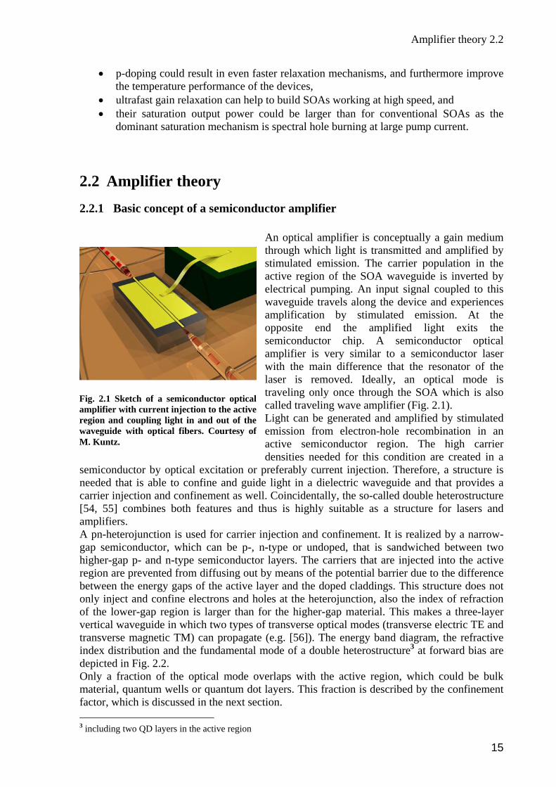
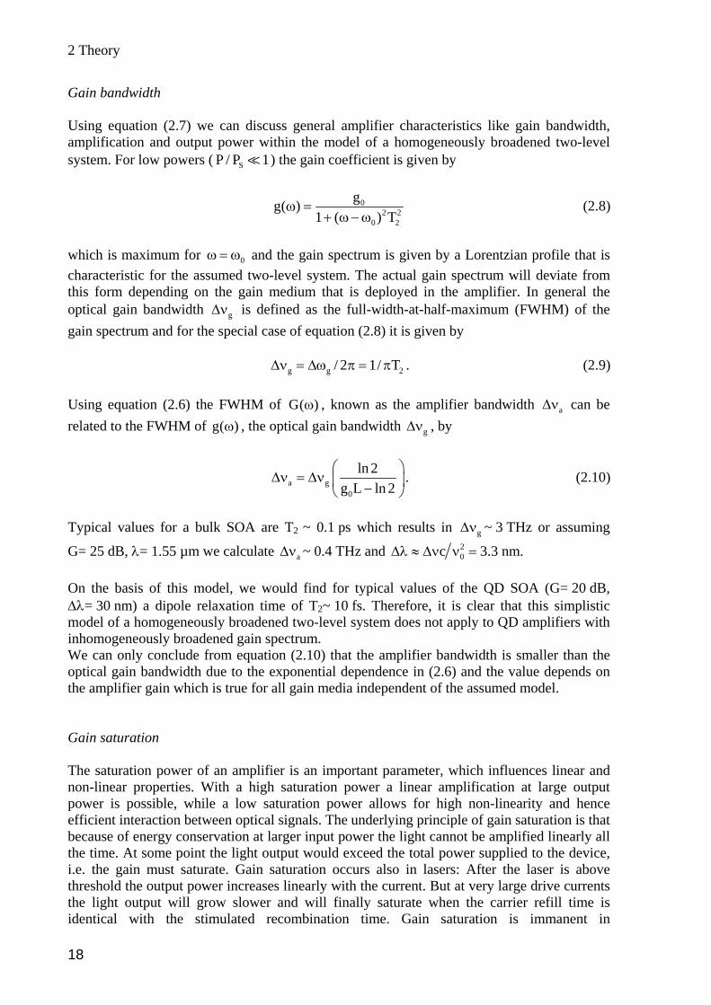
An optical amplifier is conceptually a gain medium through which light is transmitted and amplified by stimulated emission. The carrier population in the active region of the SOA waveguide is inverted by electrical pumping. An input signal coupled to this waveguide travels along the device and experiences amplification by stimulated emission. At the opposite end the amplified light exits the semiconductor chip. A semiconductor optical amplifier is very similar to a semiconductor laser with the main difference that the resonator of the laser is removed. Ideally, an optical mode is traveling only once through the SOA which is also called traveling wave amplifier (Fig. 2.1). Light can be generated and amplified by stimulated emission from electron-hole recombination in an active semiconductor region. The high carrier densities needed for this condition are created in a
semiconductor by optical excitation or preferably current injection. Therefore, a structure is needed that is able to confine and guide light in a dielectric waveguide and that provides a carrier injection and confinement as well. Coincidentally, the so-called double heterostructure [54, 55] combines both features and thus is highly suitable as a structure for lasers and amplifiers.
Fig. 2.1 Sketch of a semiconductor optical amplifier with current injection to the active region and coupling light in and out of the waveguide with optical fibers. Courtesy of M. Kuntz.
A pn-heterojunction is used for carrier injection and confinement. It is realized by a narrow-gap semiconductor, which can be p-, n-type or undoped, that is sandwiched between two higher-gap p- and n-type semiconductor layers. The carriers that are injected into the active region are prevented from diffusing out by means of the potential barrier due to the difference between the energy gaps of the active layer and the doped claddings. This structure does not only inject and confine electrons and holes at the heterojunction, also the index of refraction of the lower-gap region is larger than for the higher-gap material. This makes a three-layer vertical waveguide in which two types of transverse optical modes (transverse electric TE and transverse magnetic TM) can propagate (e.g. [56]). The energy band diagram, the refractive index distribution and the fundamental mode of a double heterostructure3 at forward bias are depicted in Fig. 2.2. Only a fraction of the optical mode overlaps with the active region, which could be bulk material, quantum wells or quantum dot layers. This fraction is described by the confinement factor, which is discussed in the next section. 3 including two QD layers in the active region
15
2 Theory
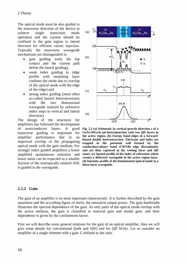
The optical mode must be also guided in the transverse direction of the device to achieve single transverse mode operation and the current should be confined to the gain region in lateral direction for efficient carrier injection. Typically the transverse waveguide mechanisms are distinguished in
• gain guiding (only the top contact and the current path define the lateral guiding),
• weak index guiding (a ridge profile with insulating layer confines the mode due to overlap of the optical mode with the edge of the ridge) and
• strong index guiding (most often so-called buried heterostructures with the two dimensional waveguide realized by refractive index steps in vertical and lateral direction).
The design of the structures for amplifiers has followed the development of semiconductor lasers. A good transverse guiding is important for amplifier performance due to an improved overlap of the propagating optical mode with the gain medium. For strongly index guided amplifiers a lower amplified spontaneous emission and lower noise can be expected as a smaller fraction of the isotropically emitted ASE is guided in the waveguide.
Fig. 2.2 (a) Schematic in vertical growth direction z of a GaAs/AlGaAs pn-heterojunction with two QD layers in the active region. (b) Energy band edges of a forward-biased double heterostructure. Electrons and holes are trapped in the potential well formed by the conduction/valence band (CB/VB) edge discontinuity and are then captured in the wetting layer and QD states. (c) Spatial profile of the index of refraction which creates a dielectric waveguide in the active region layer. (d) Intensity profile of the fundamental optical mode in a three-layer waveguide.
2.2.2 Gain The gain of an amplifier is its most important characteristic. It is further described by the gain saturation and the according figure of merit, the saturation output power. The gain bandwidth illustrates the spectral dependence of the gain. As only parts of the optical mode overlap with the active medium, the gain is classified in material gain and modal gain, and their dependence is given by the confinement factor. First we will describe some general relations for the gain of an optical amplifier, then we will give some details for conventional (bulk and QW) and for QD SOAs. Let us consider an amplifier as a single element with a gain G defined as the ratio
16
Amplifier theory 2.2
out
in
PGP
= (2.2)
where and are the optical input and output power of the amplifier.
inP P(z 0= = ) )outP P(z L= =
This ratio (2.2) is a number, if the given optical powers are in linear units, i.e. commonly in Milliwatts mW. Very often a large power range is of interest and the linear units are converted into a logarithmic unit system that is defined by
PmWPdBm 10 log1 mW
⎛ ⎞= ⋅ ⎜ ⎟
⎝ ⎠, and (2.3)
1
2
P mWdB 10 logP mW
⎛= ⋅ ⎜
⎝ ⎠
⎞⎟ (2.4)
for the optical power in decibel per 1 mW dBm and the linear ratio converted in logarithmic scale decibel dB. The amplifier equation [57]
dP gPdz
= (2.5)
relates the optical power P at a distance z from the input at z=0. For constant gain g equation (2.5) has the solution inP(z) P exp(gz)= which for a length L of the amplifier medium results in the amplifier gain ( )G exp gL= . (2.6) The optical gain depends on the wavelength or frequency of the incident signal and on the local intensity of the signal. The most general model to discuss basic behavior of the gain is a homogeneously broadened two-level system with a gain coefficient
02 2
0 2 S
gg( )1 ( ) T P / P
ω =+ ω − ω +
(2.7)
where 0 is the maximum value of the gain, g ω is the optical angular frequency of the incident gnal, 0ω is the atomic transition angular frequency, P the optical power of the signal being amplified, SP is the saturation power of the gain me um and 2T is the dipole relaxati
sii
on time4. d
This relation shows that the amplifier gain G and the optical gain g are frequency or wavelength dependent and given by ( )G( ) exp g( )Lω = ω . Both are maximum at the angular frequency , but decreases faster than 0ω = ω G( )ω g( )ω because of the exponential dependence.
4 with a typical value of 0.1 ps in a semiconductor.
17
2 Theory
Gain bandwidth Using equation (2.7) we can discuss general amplifier characteristics like gain bandwidth, amplification and output power within the model of a homogeneously broadened two-level system. For low powers ( ) the gain coefficient is given by SP / P 1
02 2
0 2
gg( )1 ( ) T
ω =+ ω − ω
(2.8)
which is maximum for and the gain spectrum is given by a Lorentzian profile that is characteristic for the assumed two-level system. The actual gain spectrum will deviate from this form depending on the gain medium that is deployed in the amplifier. In general the optical gain bandwidth
0ω = ω
g∆ν is defined as the full-width-at-half-maximum (FWHM) of the gain spectrum and for the special case of equation (2.8) it is given by . (2.9) g g / 2 1/ T∆ν = ∆ω π = π 2
Using equation (2.6) the FWHM of G( )ω , known as the amplifier bandwidth can be related to the FWHM of , the optical gain bandwidth
a∆νg( )ω g∆ν , by
a g0
ln 2g L ln 2
⎛ ⎞∆ν = ∆ν ⎜ −⎝ ⎠
⎟ . (2.10)
Typical values for a bulk SOA are T2 ~ 0.1 ps which results in g∆ν ~ 3 THz or assuming
G= 25 dB, λ= 1.55 µm we calculate ~ 0.4 THz and a∆ν 20c∆λ ≈ ∆ν ν = 3.3 nm.
On the basis of this model, we would find for typical values of the QD SOA (G= 20 dB, ∆λ= 30 nm) a dipole relaxation time of T2~ 10 fs. Therefore, it is clear that this simplistic model of a homogeneously broadened two-level system does not apply to QD amplifiers with inhomogeneously broadened gain spectrum. We can only conclude from equation (2.10) that the amplifier bandwidth is smaller than the optical gain bandwidth due to the exponential dependence in (2.6) and the value depends on the amplifier gain which is true for all gain media independent of the assumed model. Gain saturation The saturation power of an amplifier is an important parameter, which influences linear and non-linear properties. With a high saturation power a linear amplification at large output power is possible, while a low saturation power allows for high non-linearity and hence efficient interaction between optical signals. The underlying principle of gain saturation is that because of energy conservation at larger input power the light cannot be amplified linearly all the time. At some point the light output would exceed the total power supplied to the device, i.e. the gain must saturate. Gain saturation occurs also in lasers: After the laser is above threshold the output power increases linearly with the current. But at very large drive currents the light output will grow slower and will finally saturate when the carrier refill time is identical with the stimulated recombination time. Gain saturation is immanent in
18
Amplifier theory 2.2
equation (2.7) where g is reduced when becomes comparable to and therefore, the amplifier gain G decreases when P becomes large. From equations (2.7) and (2.5) in the case of the signal input at maximum gain (
P SP
0ω = ω ) follows
0
S
dP g Pdz 1 P / P
=+
, (2.11)
which is solved using the same boundary conditions as before: and
. For the large signal gain the following implicit equation is obtained: inP P(z 0= = )
)outP P(z L= =
out0
S
G 1 PG G expG P
⎛ ⎞−= −⎜
⎝ ⎠⎟
0
(2.12)
where is the unsaturated gain for small input power. As a figure of merit the 3-dB saturation output power is defined as the output power at which the gain decreases to half of its unsaturated value. Using equation (2.12) we find with its relation to by calculating
0G exp(g L)=3dBsatP
SP3dBsat 0G(P ) G / 2=
0G 100
3dB 0sat S S
0
G ln 2P P lnG 2
>
2 P= ≈ ⋅−
. (2.13)
A more general definition of the saturation output power can be used if the gain is very small (on the order of or smaller than 3 dB), then with , i.e. the point halfway between the unsaturated and the completely saturated gain. According to [58] the saturation output power and the saturation power are connected by
outsat 0G (G A) /= + 2 WGA exp( L)= −α
outsatP SP
outsat S
WG
ln 2P1
g
=α+
P (2.14)
with the waveguide losses and the modal gain g. Using this generalized definition of the saturation output power, a SOA with small device gain can still achieve a large saturation output power.
WGα
With the last equations a general description of the saturation behavior of amplifiers is at hand and the saturation output power as a figure of merit of the SOA performance is connected to the intrinsic saturation power of the gain medium. For bulk and QW material it is usually assumed that the peak gain depends on first order linearly on the carrier density N 0g ( a V)(N N )= Γ − (2.15)
19
2 Theory
with the confinement factor the differential gain coefficient ,Γ a dg dN= , the active volume V and the transparency carrier density . The carrier density changes with the injection current I and the optical signal power P according to the rate equation
0N
0
e m
dN I N a(N N ) Pdt q h
−= − −
τ σ ν (2.16)
if the number of photons is expressed by the optical power. Here, eτ is the carrier lifetime,
the effective cross section of the waveguide mode, h is Planck’s constant and ν is the frequency of the signal. For times longer than e
mστ or in continuous wave (cw)-operation we get
a stationary solution for dN sing the solution in the above equation the gain saturation is described by
dt 0= . U
0
S
gg1 P P
=+
. (2.17)
With the small signal gain given by 0 eg ( a / V)(I q N0 )= Γ τ − and the saturation power PS defined by
mS
e
hPa
1νσ=
τ (2.18)
for bulk or QWs as gain medium. For QDs it is not possible to find an analytical solution, but approximations can describe the saturation power. Using a 2-level rate equation model the relation between cw power and inversion of the active states can be found, from which the saturation power in the limit of high inversion can be approximated [59] with HI
SP
HI mS
C G
h 1 1Pa
⎛ ⎞νσ= −⎜ ⎟τ τ⎝ ⎠
(2.19)
where is the characteristic capture time (~2 ps) and Cτ Gτ is the spontaneous recombination carrier lifetime of the GS (~1 ns). This is valid under high current density where both, the QD states and the WL band edge are completely filled. The GS carrier lifetime is much larger and can be neglected in equation (2.19), hence, in this limit the gain saturation is only determined by the QD-WL spectral hole burning and limited only by the transport time into the active states. The saturation power can not be increased by further increasing the current injection because the capture time is not affected by it. Comparing the expression for bulk resp. QWs and QDs we find them similar in structure, but as the capture time is much smaller than the carrier lifetime Cτ eτ we can expect a much larger saturation power for QDs than for conventional materials. It should be noted that the approximation for the QDs assumes that the WL band edge is completely filled. This is not always achievable in real devices due to start of lasing or thermal degradation of the device.
20
Amplifier theory 2.2
Confinement factor As previously described the optical mode overlaps only partly with the region of the active medium. The fraction of the optical mode that has an overlap with the active medium is the optical confinement factor Γ. This factor is different for bulk, QW and QD material. For a typical device dimension of 2000 x 4 µm2 with a QD density of several 1010 cm-2 per layer, we can estimate about 107 quantum dots in an active zone with ten layers. Depending on the broadening, the peak material gain can be high. Yet, the overlap of the optical mode with the QD array is small. For a QD array it is on the order of total dot volume to total waveguide volume. It can be separated in an in-plane and a vertical part
( ) ( )2D DA dot
in plane vertical
N A 1 E z dz E z dzA A
∞
−∞−
Γ = ⋅ ∫ ∫ ∫ ∫2
(2.20)
with the area coverage with dots consisting of the number of QDs of average in-plane size for an area A. The vertical confinement factor is given by the vertical overlap of QDs and optical mode represented by the optical field E, averaged over the plane of area A and integrated along the vertical direction z [20]. Typical values of the total optical confinement factor for QDs are .
DN
DA
-3 -410 -10Γ =The confinement factor relates the material gain gmat of QDs, which is difficult to measure, to the modal gain g, which can be accessed via experiment and for which most of the general formulas in this section hold. The modal gain is defined as matg g= Γ (2.21) In QDs it is typically one order of magnitude lower than the maximum modal gain in QWs due to the lower confinement factor and the larger spectral width. Because of the low modal gain QD devices require a low cavity loss. It typically ranges between 2 and 10 cm-1 and has its origin in free-carrier absorption and defect center scattering. For a rectangular shaped waveguide the confinement factors of the TE and TM polarized optical mode are different. This is one reason why the gain for TE and TM modes is different and the semiconductor optical amplifiers generally exhibit a polarization dependence of the gain. The optical properties of the amplifying material have a polarization dependence itself; this is discussed in detail in section 2.2.6. Using the definitions and equations derived in this section, the gain, its bandwidth, the saturation behavior and the difference of material and modal gain of an amplifier can be understood and applied to the measurement results on a SOA.
2.2.3 Gain ripple The residual reflectivity of the chip facets has an impact on the gain of the amplifiers [60, 61]. An ideal amplifier should have no reflectivity at the end facets yielding a perfect traveling wave device. In practice, even with several means of reducing the reflectivity, as seen in chapter 2.3.2, some residual reflectivity forms an optical cavity. Therefore, the gain of the
21
2 Theory
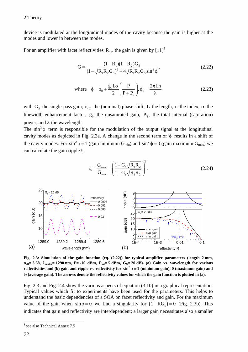
device is modulated at the longitudinal modes of the cavity because the gain is higher at the modes and lower in between the modes. For an amplifier with facet reflectivities the gain is given by [11]5 1,2R
1 2 S2
1 2 S 1 2 S
(1 R )(1 R )GG(1 R R G ) 4 R R G sin2
− −=
− + φ, (2.22)
where 00 0
S
g L P 2 Ln,2 P P
⎛ ⎞α πφ = φ + φ =⎜ ⎟+ λ⎝ ⎠
(2.23)
with the single-pass gain, the (nominal) phase shift, L the length, the index, α the linewidth enhancement factor, the unsaturated gain, the total internal (saturation) power, and λ the wavelength.
SG (0)φ n
0g (S)P
The term is responsible for the modulation of the output signal at the longitudinal cavity modes as depicted in Fig. 2.3a. A change in the second term of
2sin φφ results in a shift of
the cavity modes. For 1 (gain minimum Gmin) and 2sin φ = 2sin φ = 0 (gain maximum Gmax) we can calculate the gain ripple ξ
2
s 1 2max
min s 1 2
1 G R RGG 1 G R R
⎛ ⎞+ξ = = ⎜⎜ −⎝ ⎠
⎟⎟ . (2.24)
1289.0 1289.2 1289.4 1289.6
10
15
20
25
(a)
GS= 20 dB
reflectivity 0.0003 0.001 0.003
0.03
gain
(dB)
wavelength (nm)1E-4 1E-3 0.01 0.105
10152025
R*GS-1=0
gain
(dB)
reflectivity R
max gain avg gain min gain
GS= 20 dB0369
rippl
e (d
B)
(b)
Fig. 2.3: Simulation of the gain function (eq. (2.22)) for typical amplifier parameters (length 2 mm, neff= 3.68, λcenter= 1290 nm, P= -10 dBm, Psat= 5 dBm, GS= 20 dB). (a) Gain vs. wavelength for various reflectivities and (b) gain and ripple vs. reflectivity for 2sin φ = 1 (minimum gain), 0 (maximum gain) and ½ (average gain). The arrows denote the reflectivity values for which the gain function is plotted in (a). Fig. 2.3 and Fig. 2.4 show the various aspects of equation (3.10) in a graphical representation. Typical values which fit to experiments have been used for the parameters. This helps to understand the basic dependencies of a SOA on facet reflectivity and gain. For the maximum value of the gain when sin we find a singularity for 0φ = ( )s1 RG 0− = (Fig. 2.3b). This indicates that gain and reflectivity are interdependent; a larger gain necessitates also a smaller
5 see also Technical Annex 7.5
22
Amplifier theory 2.2
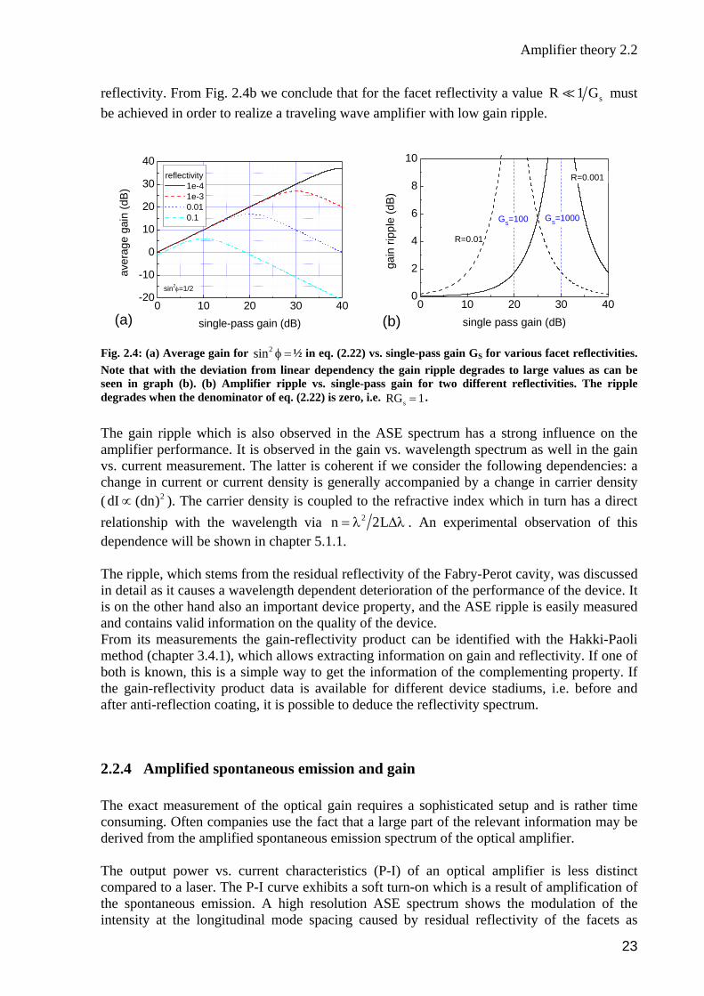
reflectivity. From Fig. 2.4b we conclude that for the facet reflectivity a value sR 1 G must be achieved in order to realize a traveling wave amplifier with low gain ripple.
0 10 20 30 40-20
-10
0
10
20
30
40
(a)
aver
age
gain
(dB
)
single-pass gain (dB)
reflectivity 1e-4 1e-3 0.01 0.1
sin2φ=1/2
0 10 20 30 400
2
4
6
8
10
(b)
R=0.001
gain
ripp
le (d
B)
single pass gain (dB)
GS=100 GS=1000
R=0.01
Fig. 2.4: (a) Average gain for ½ in eq. (2.22) vs. single-pass gain GS for various facet reflectivities. Note that with the deviation from linear dependency the gain ripple degrades to large values as can be seen in graph (b). (b) Amplifier ripple vs. single-pass gain for two different reflectivities. The ripple degrades when the denominator of eq. (2.22) is zero, i.e.
2sin φ =
sRG 1= .
The gain ripple which is also observed in the ASE spectrum has a strong influence on the amplifier performance. It is observed in the gain vs. wavelength spectrum as well in the gain vs. current measurement. The latter is coherent if we consider the following dependencies: a change in current or current density is generally accompanied by a change in carrier density ( ). The carrier density is coupled to the refractive index which in turn has a direct relationship with the wavelength via
2dI (dn)∝2n 2L= λ ∆λ . An experimental observation of this
dependence will be shown in chapter 5.1.1. The ripple, which stems from the residual reflectivity of the Fabry-Perot cavity, was discussed in detail as it causes a wavelength dependent deterioration of the performance of the device. It is on the other hand also an important device property, and the ASE ripple is easily measured and contains valid information on the quality of the device. From its measurements the gain-reflectivity product can be identified with the Hakki-Paoli method (chapter 3.4.1), which allows extracting information on gain and reflectivity. If one of both is known, this is a simple way to get the information of the complementing property. If the gain-reflectivity product data is available for different device stadiums, i.e. before and after anti-reflection coating, it is possible to deduce the reflectivity spectrum.
2.2.4 Amplified spontaneous emission and gain The exact measurement of the optical gain requires a sophisticated setup and is rather time consuming. Often companies use the fact that a large part of the relevant information may be derived from the amplified spontaneous emission spectrum of the optical amplifier. The output power vs. current characteristics (P-I) of an optical amplifier is less distinct compared to a laser. The P-I curve exhibits a soft turn-on which is a result of amplification of the spontaneous emission. A high resolution ASE spectrum shows the modulation of the intensity at the longitudinal mode spacing caused by residual reflectivity of the facets as
23
2 Theory
discussed in chapter 2.2.3. For bulk and quantum well based amplifiers the amplified spontaneous emission spectrum shifts to the blue (shorter wavelengths) with increasing current. This is primarily due to the filling of the band with injected electrons and holes [57]. The optical gain, current and ASE are related and can be calculated as described for bulk and QWs in [11, 62, 63]. A gain proportional to the carrier density, a parabolic gain wavelength characteristic and a peak wavelength that is a function of the carrier density are assumed giving a good approximation for the characteristics of bulk and QW SOAs. The most important result is the proportionality of ASE and gain from which we can expect a similarity in their spectrum and their absolute value of the gain ripple. For QDs no such simple relations can be given for gain and ASE because a sophisticated model is needed that describes the properties of QDs and their surrounding WL and barrier material. Such a model has been implemented by Berg [59] showing the crucial role of ASE in QD SOAs, especially for long (>5 mm) devices at high current densities. The interrelation of ASE and gain for QD SOAs will be experimentally investigated in section 5.1.1.
2.2.5 Noise Within the amplifying section of a SOA the ground state can recombine through stimulated emission caused by a signal photon or spontaneously with random direction and phase. Some of the spontaneously emitted photons will be amplified which results in amplified spontaneous emission (ASE). This and other contributions of the noise degrade the overall performance of the amplifier as it they are added to the input and amplified signal. In this section the noise properties are analyzed in detail to understand the different roles of the individual noise contributions. For an optical amplifier the following general consideration from [64] applies. The total ASE power PASE or the ASE density ρASE summed over all modes in an optical bandwidth equals to
0B
(2.25) ASE sp 0 ASE spP 2n h (G 1)B or 2n h (G 1)= ν − ρ = ν − with the spontaneous emission factor as a measure of the quality of inversion of the optical amplifier given by
spn
2sp
2 1
NnN N
=−
(2.26)
with N1,2 the occupation probability of the ground and the excited level. Intensity/Photocurrent noise Discussions about the basic conversion of light intensity into electrical current by an optical receiver can be found in many books and articles [7, 13, 64-67]. In order to understand the noise figure, this discussion is reviewed shortly at this point. The average photocurrent generated in a photodetector by an optical source is dci = ℜ P with average power
2P E (t= ) where the detector responsivity is defined as q / h [A / W]ℜ = η ν with q the
24
Amplifier theory 2.2
charge of t cyhe carriers. The light collection quantum efficien η includes all o
taneous beat noise noise
ted further below. We consider an amplified
ptical losses that are part of the optical receiver. Not only is the average optical power, but also intensity noise is present in the amplifier which is a significant limiting factor in optical communication systems. The amplitude of the optical field noise is directly converted by the photodetector into electrical noise, while the phase noise can be converted to intensity noise via interference effects. The following intensity noise types are commonly encountered in optical systems and result in a contribution to the noise figure:
• Shot noise • Signal-spon• Spontaneous-spontaneous beat • Interference noise
For the following equations the variables are lissignal light together with ASE incident on a detector with their total electric field expressed as6
0
0
B / 2
in 0 ASE 0 kk B / 2
E(t) 2GP cos( t) 2 cos(( 2 k )t )δν
=− δν
= ω + ρ δν ⋅ ω + π δν∑ + Ω (2.27)
Hence,
0
0
0
0
2
inB / 2
in ASE 0 0 kk B / 2
2B / 2
ASE 0 kk B / 2
i(t) E (t)GP (signal)
4 GP cos( t) cos(( 2 k )t ) (sig-sp beat noise)
2 cos(( 2 k )t ) (sp-sp beat noise)
δν
=− δν
δν
=− δν
= ℜ= ℜ
+ ℜ ρ δν ⋅ ω ω + π δν + Φ
⎡ ⎤+ ℜρ δν ⋅ ω + π δν + Φ⎢ ⎥
⎣ ⎦
∑
∑
(2.28)
etric addition theorems and symmetry arguments yields
and application of trigonom
0
0
0 0
inB / 2
in ASE kk B / 2
B / B /
ASE k jk 0 j 0
i(t) GP (signal)= ℜ
2 GP cos(2 k t ) (sig-sp beat noise)
2 cos((k j)2 t ) (sp-sp beat noise)
δν
=− δν
δν δν
= =
+ ℜ ρ δν π δν + Φ
+ ℜρ δν ⋅ − πδν + Φ − Φ
∑
∑ ∑
(2.29)
ply the detected signal. It has an underlying shot noise process with the
ig= ℜ (2.30)
The first term is simvariance or noise power spectral density
σsig shot
2i s2q P
−
6 (Factor 2 arises from normalization, because 2cos (t) 1/ 2= ).
25
2 Theory
T the second and third term fluctuate he phase of the ASE fluctuates randomly, thus ccordingly, which results in noise. Because these terms have no correlation, they can be a
treated individually and the noise power of each term is given by the variance 22 2i i iσ = − .
Assuming that the ASE is wavelength independent around the signal wavelength, the power density of the signal-spontaneous beat noise is evaluated to
sig sp ASE
2 2i sig4 GP
−σ = ℜ ρ
or the spontaneous-spontaneous beat noise (third ter
btained for . This results in a shot noise of 2q Bσ = ℜρ
ity near dc of
2)
or amplifiers that are polarization dependent, i.e. theyE and TM polarization, ASE (copolarized with the signal) has to be accounted for.
noise figure is explicitly defined as [2, 68]:
propagation of a shot-noise-
There n the
put inear representation of the
. (2.31) F m) the dc current dc
sp ASE 0I B= ℜρ is
o k j=sp shot SE 0−
remaining sum terms according to their frequency one obtains the power dens
sp sp
2 2 2i ASE 02 B
−σ ℜ ρ (2.3
2i A . By organizing the
F have a different single-pass gain for T ASEρThis leads to a polarization dependent noise figure.
oise Figure N The so-called
The decrease of the signal-to-noise ratio (SNR), at the output of an optical detector with unitary quantum efficiency, due to thelimited signal through the optical amplifier expressed in dB.
fore, the noise figure of an amplifier describes the degradation of the SNR betwee and the output of the amplifier. The noise factor F is the lin
noise figure NF with the following relation NF 10 log(F)= (2.33) a nal-to-noise ratios by nd the noise factor is defined in terms of electrical sig
inSNRFSNR
= out
(2.34)
sing the above derived contributions of the signa
se, the spontaneous shot noise and the
noise factor of
U l shot noise, the signal-spontaneous beat noise, the spontaneous-spontaneous beat noicontribution from multi-path interference noise, we obtain
sig shot
2 2 2in dc i sig sigSNR i / ( P ) /(2q P )
−= σ = ℜ ℜ ;
sig shot sig sp sp sp sp shot MPI
2 2 2 2 2 2out dc,out i i i i iSNR i /( )
− − − −= σ + σ + σ + σ + σ
2 2 2 2 2sig sig sig ASE ASE 0 ASE 0 MPI(G P ) /(2qG P 4 GP 2 B 2q B )= ℜ ℜ + ℜ ρ + ℜ ρ + ℜρ + σ which equals a
26
Amplifier theory 2.2
ASE
2ASE sp-sp 2ASE
MPI2 2sig sig
sig-shot sig-sp sp-sp sp-shot MPI
2 B1 PF fG Gh 2h G P G P
F F F F F
ηρ ρ= + + + + ⋅ σ
ν ν
= + + + +
actor
(2.35)
with sigMPI i cav,i2
i
2PF (
h f∆ν
=νπ + ∆ν ∑ p G )
here is the gain at the signal wavelength,
sity of spontaneous emission,
w G is the collection quantum efficiency, η
ASEρ is the unpolarized optical power den
ASEρ is the with the signal copolarized ASE density,
cν =
λ is the signal frequency, with speed of light c and wavelength λ,
sp-sp 20
cB( )
∆λ≅
λ is the equivalent optical bandwidth of the ASE in Hz,
is the optical input power, er over wavelength,
p G esonator which takes the
is ti
he noise factor due to multipath interference (MPI), , is generated by the beating
or most cases the signal-spontaneous beat noise contribution is dominant while ASE shot
sigP is the integrated ASE powASEP
i cav,i is the effective resonator gain of the ith rpolarization state of the signals into account, he FWHM of the source linewidth, and ∆ν
f s the base band frequency.
T MPIFbetween the output signal and one or more doubly reflected replicas of the output signal. Two or more reflection points inside the amplifier are necessary to generate MPI noise. MPI noise cannot be derived from the ASE as measured on an optical spectrum analyzer. It must be measured after a broadband optical-to-electrical conversion on an electrical spectrum analyzer. Fnoise and multiple path interference contributions are neglected. Using the first two terms of (2.35) and (2.25) with ASE A1 2 SEρ = ρ and assuming we
r = =
G 1find for spn 1= the minimum value for the noise facto 3dB NF= . For perfect population inversion ( spn 1
spF 2n 2= ), there is no stimulated absorption, and a quantum-
wa
limited noise figure is achieved. mperfect population inversion, on the other hand, stimulated absorption occurs, which increases the noise figure. This consideration indicates that the stimulated absorption causes noise figure degradation. For semiconductor amplifiers
spn ranges from 1.4 to more than 4 depending both on the pumping rate and the operating velength.
For i
27

2 Theory
0 5 10 15 200.0
0.5
1.0
1.5
2.0
2.5
3.0
3.5
NF
corre
ctio
n fa
ctor
(dB
)
∆Gpol (dB)
Fig. 2.5: Correction of the noise figure for TE modes vs. polarization dependence of the amplifier gain showing a maximum correction of 3 dB for large polarization difference for TE/TM modes. The polarization dependence of an amplifier is defined as ( )pol TE TMG 10log G G∆ = . If
, i.e. the amplifier is polarization independent, then the only polarization dependent part of the noise figure yields
G 0∆ =
G 0 ASEF∆ = = ρ νGh . According to [69] the correction of the noise figure for TE modes is
ASE,TM TM
TEASE,TE
TEGGG 0
F ( G) 2 2F 11 ρ
∆ = ρ
∆= ≈
++ (2.36)
using the fact that and the proportionality of formula (2.25) with
for large gain. As can be seen on Fig. 2.5, the corrective factor is as high as 3 dB for strongly polarized SOAs.
ASE ASE,TE ASE,TMρ = ρ + ρ
ASE,TE / TM TE / TMGρ ∼
In summary, the elaborate derivation of the noise figure allows an insight in the different contributions, their physical origin and their weight in the noise figure. Using equation (2.35) we are able to derive the noise figure of an amplifier, which is described by method in section 4.2.3 and the measurement in section 5.1.2. It was shown that the noise figure is sensitive on the polarization dependence of the gain, which must be taken into account when measuring the noise figure.
2.2.6 Polarization properties of amplifiers The polarization properties of SOAs are of interest for the performance of these elements in optical systems. In data transmission systems were SOAs can be deployed as booster, in-line or pre-amplifiers polarization insensitive operation is demanded for the latter two applications. For the two polarization states we adhere to the definition given in chapter 2.3.2. In the case of the transverse-magnetic (TM)-mode the polarization is aligned with the z-direction. For the transverse-electric (TE)-mode the polarization vector is along the xy-plane. The polarization sensitivity of SOAs results at first from the difference of the confinement factor for the TE- and TM-modes in the waveguide which contribute to the different TE and TM signal amplification. Additionally, the gain medium can amplify the two polarizations
28
Amplifier theory 2.2
differently. This is the case for QW SOAs where different quantization levels for heavy hole (HH) bands (which are the dominant part of the optical gain for the TE-mode) and light-hole (LH) bands (which are the part of the optical gain for the TM-mode) lead to a polarization sensitivity of the gain medium. In bulk material HH and LH are degenerate in the valence band which results in a polarization insensitive material gain. For the design of polarization insensitive SOAs many approaches exist which have been successfully implemented for bulk and QW SOAs.
a) A thick active layer reduces the difference in the confinement factor between TE- and TM-mode (mostly realized for bulk)
b) An anisotropic gain coefficient of the active layer compensates the difference in the modal confinement factor. In QW SOAs the HH and LH energies can be shifted by strain which results in a polarization insensitive amplifier [70-74].
c) A non-planar waveguide structure (more square-like) results in a comparably large confinement-factor, but a very narrow waveguide and large coupling losses.
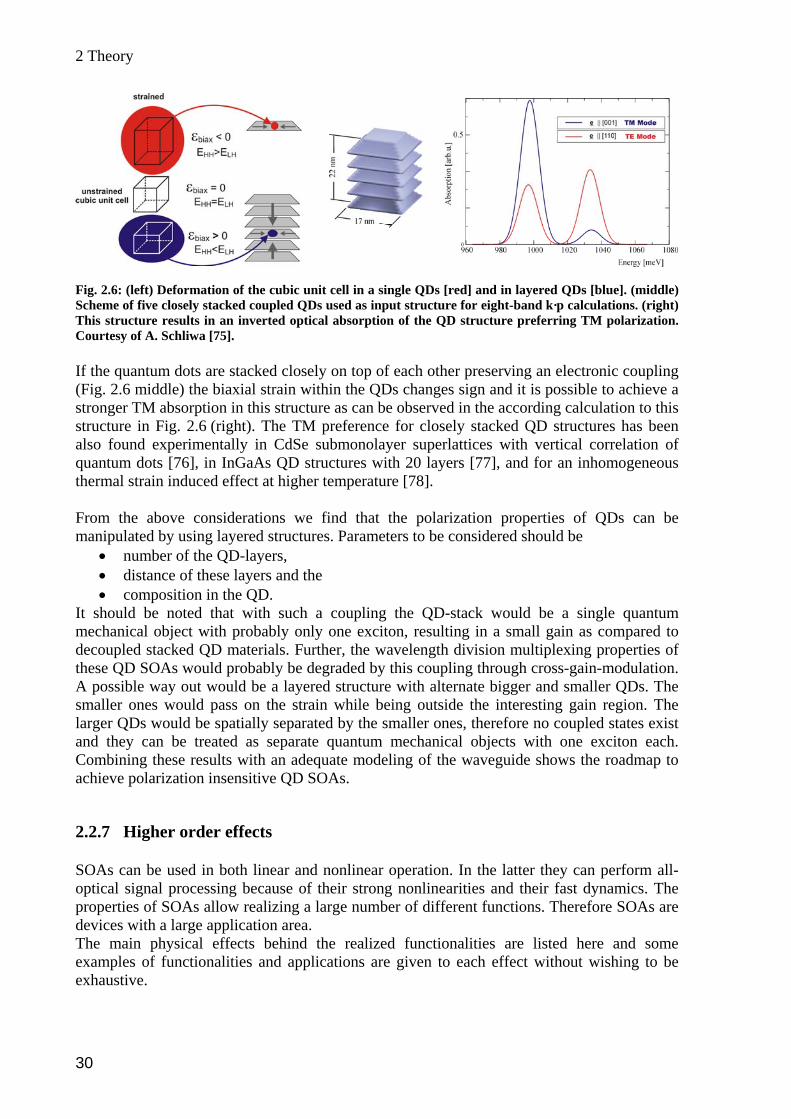
QDs as an active medium offer potential advantages with regards to polarization because their electronic wavefunctions can be tailored to some extend by growth. Detailed eight-band k·p modeling to calculate the electronic structure of QDs has been carried out by A. Schliwa [75]. With information on size, shape and composition of the QDs it is possible to compute the single- and multi-particle states, oscillation strength and polarization of optical transitions. In general single QDs show a dominant transition to the heavy hole projection of the hole state which is transverse electrically polarized. The optical transition to the light hole projection would be transverse magnetic, but has only a small contribution for a single dot which is mainly due to the biaxial strain distribution in the disk like QD. Calculations of the polarization anisotropy of quantum dots show a strong anisotropy between the TM and the TE polarization direction. The reason is – similar to the quantum wells – the different position of the HH- and LH-bands. A typical hole ground state of a pyramidal InAs QD shows 89% HH- and only 8.4% LH-contribution. This situation changes fundamentally in layered structures. We start with a short description about the reason for HH-LH splitting. Possible deformations of a cubic unit cell are a volume change (hydrostatic strain, ) or a change of the axial ratio. The latter is the biaxial strain (
hydroε
biaxε ) defined by with εxx,yy,zz the strain along the crystal directions and r the
radial vector. This biaxial strain determines the relative energetic position of HH- to LH-band (at the Γ-point):
( ) ( ) ( ) ( )biax xx yy zzr r r 2ε = ε + ε − ε r
( ) ( ) ( )( ) ( ) ( )
HH V hydro biax
LH V hydro biax InAs
V r a r b 2 r
V r a r b 2 r with b 0
= ε + ε
= ε − ε < (2.37)
In a single QD (Fig. 2.6 red) we have ( ) ( ) ( )xx yy zzr r 2 rε + , ε < ε ( )biax r 0ε < and therefore, the HH-band lies energetically above the LH-band. In layered structures we have the blue coded situation in Fig. 2.6: ( ) ( ) ( )xx yy zzr r 2 rε + ε > ε , ( )biax r 0ε > , meaning HH-band and LH-band move towards each other and possibly change their energetic position. HH-fractions of a hole wavefunction emit solely TE-polarized light, while LH-fractions are dominantly TM-polarized.
29
2 Theory
Fig. 2.6: (left) Deformation of the cubic unit cell in a single QDs [red] and in layered QDs [blue]. (middle) Scheme of five closely stacked coupled QDs used as input structure for eight-band k·p calculations. (right) This structure results in an inverted optical absorption of the QD structure preferring TM polarization. Courtesy of A. Schliwa [75]. If the quantum dots are stacked closely on top of each other preserving an electronic coupling (Fig. 2.6 middle) the biaxial strain within the QDs changes sign and it is possible to achieve a stronger TM absorption in this structure as can be observed in the according calculation to this structure in Fig. 2.6 (right). The TM preference for closely stacked QD structures has been lso found experimentally in CdSe submonolayer superlattices with vertical correlation of
rations we find that the polarization properties of QDs can be
h division multiplexing properties of ese QD SOAs would probably be degraded by this coupling through cross-gain-modulation.
region. The larg Q arated by the smaller ones, therefore no coupled states exist and uantum mechanical objects with one exciton each. Com ining these results with an odeling of the waveguide shows the roadmap to
n to each effect without wishing to be
aquantum dots [76], in InGaAs QD structures with 20 layers [77], and for an inhomogeneous thermal strain induced effect at higher temperature [78].
rom the above consideFmanipulated by using layered structures. Parameters to be considered should be
• number of the QD-layers, • distance of these layers and the • composition in the QD.
It should be noted that with such a coupling the QD-stack would be a single quantum mechanical object with probably only one exciton, resulting in a small gain as compared to decoupled stacked QD materials. Further, the wavelengtthA possible way out would be a layered structure with alternate bigger and smaller QDs. The smaller ones would pass on the strain while being outside the interesting gain
er Ds would be spatially sep they can be treated as separate q
adequate mbachieve polarization insensitive QD SOAs.
2.2.7 Higher order effects SOAs can be used in both linear and nonlinear operation. In the latter they can perform all-optical signal processing because of their strong nonlinearities and their fast dynamics. The properties of SOAs allow realizing a large number of different functions. Therefore SOAs are devices with a large application area. The main physical effects behind the realized functionalities are listed here and some xamples of functionalities and applications are givee
exhaustive.
30
Amplifier theory 2.2
Linear effects o Optical gain
The signal is amplified by stimulated emission Function: booster-, inline-, pre-amplification
tion: broadband light source
cts dulation (SPM)
y refractive index changes induced by
ation o
ed by the variation of the signal input power unction: waveform distortion compensation
Modulation (XGM) optical signal that affects the gain of all the other
lexing, label swapping, clock recovery o
by one optical beam affecting the output phase of all
sampling, wavelength conversion,
o ating along the SOA generates beams at new
plexing, wavelength conversion, XOR gate The op us sections. Here, we will present some details The oth not be further reviewed. XG usually a weak probe signal, are present in an amplifier this effect occurs. In satu hanges
ue to the pump wavelength have an inverse effect on the gain which is available for the
een the channels occurs by XGM. he maximum operation speed of the wavelength converter based on XGM is limited due to
rable to the
o Amplified Spontaneous Emission (ASE) Consists of spontaneously emitted photons amplified along the active waveguide Func
Non-linear effeo Self Phase Mo
Modulation of the output signal phase caused bthe power variations of the same signal Function: waveform shaping, chirp compensSelf Gain Modulation (SGM) Modulation of the signal gain inducF
o Cross GainGain modulation induced by oneoptical beams propagating in the SOA Function: wavelength conversion, multipCross Phase Modulation (XPM) Refractive index changes inducedthe other signals propagating along the SOA Function: add/drop multiplexing, opticalregeneration Four-Wave mixing (FWM) Beating of two or more signals propagoptical frequencies Function: optical sampling, demulti
tical gain and ASE were described in previoon XGM as this effect was studied with our QD SOAs by experiments (section 5.2.4). er effects will
M results from gain saturation in a SOA. If two signals with different wavelengths, a strong pump and ration the available gain is distributed between the two wavelengths and the c
dprobe wavelength. Thereby, data can be transferred from one wavelength to the other, so-called wavelength conversion, but on the other hand the effect is unwanted for amplification of multiple wavelengths where a cross talk betwTthe gain recovery time, which results from the change of the total carrier density in the active region of bulk or QW SOAs. An ultrafast gain recovery time has been reported for QD SOAs [52] which would predict a faster operation with XGM. There have been already reports on XGM with quantum dot SOAs where wavelength conversion by XGM without patterning of a 10 Gbit/s data signal was experimentally demonstrated [40]. Other papers reported a small-signal 3dB XGM bandwidth of 1.5 GHz with an InP-based 1550 nm quantum dash SOA [79] and a bandwidth of 3.5 GHz in a p-doped QD SOA at 1.3 µm [80] which is compastructures introduced in this thesis.
31
2 Theory
The XGM can be tested with a small-signal measurement where a strong saturating pump signal is modulated by an electro-optical modulator. The modulation amplitude is much smaller than the signal amplitude to achieve a small-signal modulation which is transferred in a gain modulation which in turn is probed by the second wavelength cw signal. The small signal conversion efficiency from the pump to the probe wavelength is given by [57]
s se s1 i2 f
gLexp 1⎛ ⎞−
η = −⎜ ⎟τ τ (2.38)
+ + π τ⎝ ⎠ where seτ is the spontaneous emission carrier lifetime and sτ is the stimulated emission carrier lifetime which can be deduced from
p
s s
P1E
=τ
at
(2.39)
ith the probe power pP and the saturation energy sat sat seE P= ⋅ τw . Typical XGM bandwidths
sting as it allows wavelength conversion. According to the ynamic properties of QD SOAs even parallel w
s feasible: A fast XGM operation based on spectral hole burning can be m avelength sub
r depletion
order to understand basic properties of the optical waveguide, simulations with a pure ptical modeling tool were done.
design) program [81] allows and is able to simulate the
ansmission of this mode in a waveguide with a beam propagation method. The ridge waveguide profile of the SOA is simulated using a 2D mode solver which calculates the
n and the effective refractive index of the ridge waveguide tructure. The simulation tool accounts only for optical influences via a complex refractive
mode solver featuring the optical mode and the underlying
are in the range of 1-10 GHz, depending on the optical power of the probe as seen from the above formula. The XGM effect is very intered avelength conversion with two or more wavelengths seemrealized within the ho ogeneous broadening of the w -ensemble, while the inhomogeneous broadening is dominated by carrie resulting in a small XGM bandwidth, and thereby a small interdependence of neighboring wavelengths. 2.3 Simulation and modeling of QD SOAs
2.3.1 Waveguide simulations InoThe BPM-CAD (beam propagation method - computer aided calculating the two-dimensional mode of a waveguide profiletr
optical near field, modal distributiosindex, while current injection, carrier densities and thermal effects are not included. Fig. 2.7(a) shows a typical result of theridge waveguide profile for a deeply etched 2 µm mesa. The modeled structure has to be simplified compared to the epitaxial structure of the sample (see section 3.2). No capping layer is included, the graded layers and the QD layers are approximated with an averaged refractive index.
32
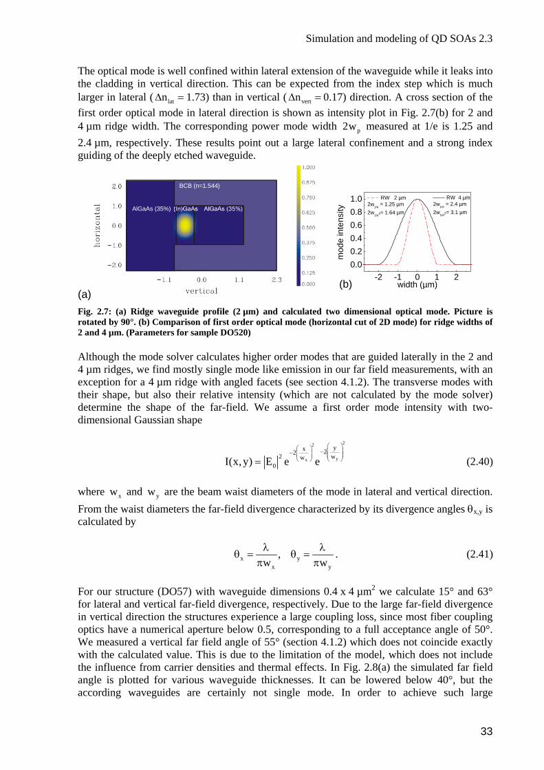
Simulation and modeling of QD SOAs 2.3
The optical mode is well confined within lateral extension of the waveguide while it leaks into the cladding in vertical direction. This can be expected from the index step which is much larger in lateral ( latn∆ = 1.73) than in vertical ( vertn∆ = 0.17) direction. A cross section of the first order optical mode in lateral direction is shown as intensity plot in Fig. 2.7(b) for 2 and 4 µm ridge width. The corresponding power mode width p2w measured at 1/e is 1.25 and
.4 µm, respectiv2 ely. These results point out a large lateral confinement and a strong index
(a)
guiding of the deeply etched waveguide.
AlGaAs (35%) AlGaAs (35%)(In)GaAs
B
0.8
CB (n=1.544)
0.40.6
1.0
-2 -1 0 1 20.00.2
inte
nsity
mod
e
width (µm)
RW 4 µm2w1/e = 2.4 µm2w1/e2= 3.1 µm
(b)
RW 2 µm2w1/e = 1.25 µm2w1/e2= 1.64 µm
Fig. 2.7: (a) Ridge waveguide profile (2 µm) and calculated two dimensional optical mode. Picture is rotated by 90°. (b) Comparison of first order optical mode (horizontal cut of 2D mode) for ridge widths of 2 and 4 µm. (Parameters for sample DO520) Although the mode solver calculates higher order modes that are guided laterally in the 2 and 4 µm ridges, we find mostly single mode like emission in our far field measurements, with an
eption for a 4 µm ridge with angled facets (see section 4.1.2). The transverse modes with exctheir shape, but also their relative intensity (which are not calculated by the mode solver) determine the shape of the far-field. We assume a first order mode intensity with two-dimensional Gaussian shape
22
yx
yx 222 ww0I(x, y) E e e
⎛ ⎞⎛ ⎞ − ⎜ ⎟− ⎜ ⎟ ⎜ ⎟⎝ ⎠ ⎝ ⎠= (2.40)
where xw and yw are the beam waist diameters of the mode in lateral and vertical direction. From the waist diameters the far-field divergence characterized by its divergence angles θx,y is alculated by
c
x yx y
,w wλ λ
θ = θ =π π
. (2.41)
ction the structures experience a large coupling loss, since most fiber coupling ptics have a numerical aperture below 0.5, corresponding to a full acceptance angle of 50°. e measured a vertical far field angle of 55° (section 4.1
with the calculated value. This is due to the limitation of the model, which does not include e influence from carrier densities and thermal effects. In Fig. 2.8(a) the simulated far field
For our structure (DO57) with waveguide dimensions 0.4 x 4 µm2 we calculate 15° and 63° for lateral and vertical far-field divergence, respectively. Due to the large far-field divergence n vertical direi
oW .2) which does not coincide exactly
thangle is plotted for various waveguide thicknesses. It can be lowered below 40°, but the according waveguides are certainly not single mode. In order to achieve such large
33
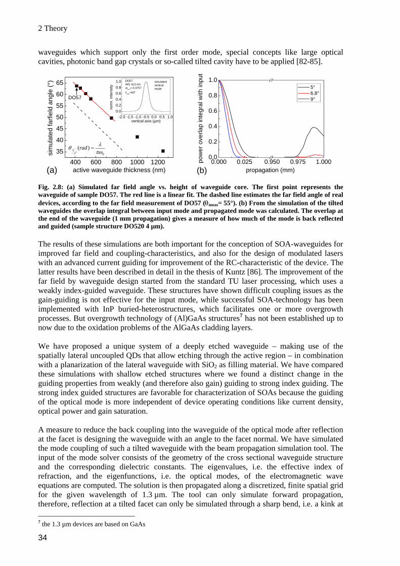
2 Theory
waveguides which support only the first order mode, special concepts like large optical cavities, photonic band gap crystals or so-called tilted cavity have to be applied [82-85].
50
55
60
65
0.6
0.8
1.0
400 600 800 1000 120035
40
45
-2.0 -1.5 -1.0 -0.5 0.0 0.5 1.00.00.20.40.60.81.0
norm
. int
ensi
ty
vertical axis (µm)
DO57 WG 413 nmw1/e²= 0.3757θ1/e2=63°
simulated vertical mode
01 )(
2 πωλθ =rad
esim
ulat
e
active waveguide thickness (nm)
DO57
d fa
rfiel
d an
gle
(°)
(a)0.000 0.025 0.950 0.975 1.000
0.0
0.2
0.4
(b)
pow
er o
verla
p in
t
propagation (mm)
egra
l with
inpu
t
5° 6.8° 9°
Fig. 2.8: (a) Simulated far field angle vs. height of waveguide core. The first point represents the waveguide of sample DO57. The red line is a linear fit. The dashed line estimates the far field angle of real devices, according to the far field measurement of DO57 (θmeas= 55°). (b) From the simulation of the tilted waveguides the overlap integral between input mode and propagated mode was calculated. The overlap at the end of the waveguide (1 mm propagation) gives a measure of how much of the mode is back reflected and guided (sample structure DO520 4 µm).
rom the standard TU laser processing, which uses a eakly index-guided waveguide. These structures have shown difficult coupling issues as the
strong index guiding. The trong index guided structures are favorable for characterization of SOAs because the guiding
constants. The eigenvalues, i.e. the effective index of fraction, and the eigenfunctions, i.e. the optical modes, of the electromagnetic wave
The results of these simulations are both important for the conception of SOA-waveguides for improved far field and coupling-characteristics, and also for the design of modulated lasers with an advanced current guiding for improvement of the RC-characteristic of the device. The latter results have been described in detail in the thesis of Kuntz [86]. The improvement of the far field by waveguide design started fwgain-guiding is not effective for the input mode, while successful SOA-technology has been implemented with InP buried-heterostructures, which facilitates one or more overgrowth processes. But overgrowth technology of (Al)GaAs structures7 has not been established up to now due to the oxidation problems of the AlGaAs cladding layers. We have proposed a unique system of a deeply etched waveguide – making use of the spatially lateral uncoupled QDs that allow etching through the active region – in combination with a planarization of the lateral waveguide with SiO2 as filling material. We have compared these simulations with shallow etched structures where we found a distinct change in the guiding properties from weakly (and therefore also gain) guiding to sof the optical mode is more independent of device operating conditions like current density, optical power and gain saturation. A measure to reduce the back coupling into the waveguide of the optical mode after reflection at the facet is designing the waveguide with an angle to the facet normal. We have simulated the mode coupling of such a tilted waveguide with the beam propagation simulation tool. The input of the mode solver consists of the geometry of the cross sectional waveguide structure and the corresponding dielectric reequations are computed. The solution is then propagated along a discretized, finite spatial grid for the given wavelength of 1.3 µm. The tool can only simulate forward propagation, therefore, reflection at a tilted facet can only be simulated through a sharp bend, i.e. a kink at
7 the 1.3 µm devices are based on GaAs
34
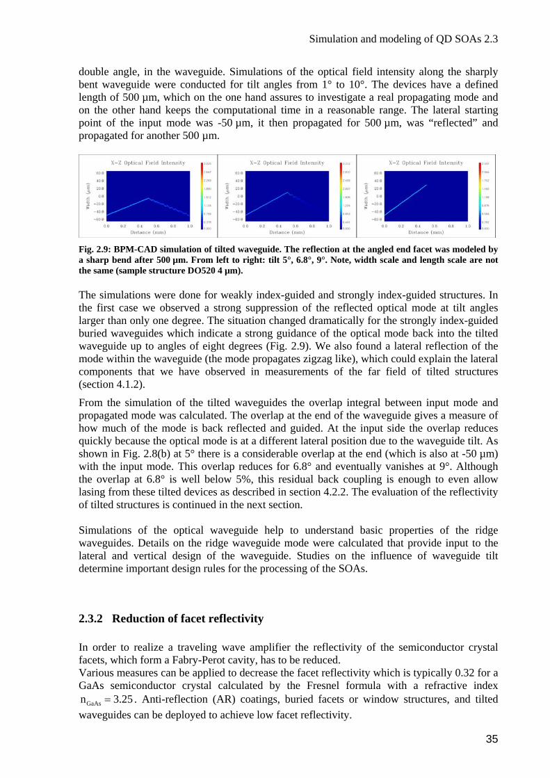
Simulation and modeling of QD SOAs 2.3
double angle, in the waveguide. Simulations of the optical field intensity along the sharply bent waveguide were conducted for tilt angles from 1° to 10°. The devices have a defined length of 500 µm, which on the one hand assures to investigate a real propagating mode and on the other hand keeps the computational time in a reasonable range. The lateral starting point of the input mode was -50 µm, it then propagated for 500 µm, was “reflected” and propagated for another 500 µm.
Fig. 2.9: BPM-CAD simulation of tilted waveguide. The reflection at the angled end facet was modeled by a sharp bend after 500 µm. From left to right: tilt 5°, 6.8°, 9°. Note, width scale and length scale are not the same (sample structure DO520 4 µm). The simulations were done for weakly index-guided and strongly index-guided structures. In the first case we observed a strong suppression of the reflected optical mode at tilt angles
ees (Fig. 2.9). We also found a lateral reflection of the ode within the waveguide (the mode propagates zigzag like), which could explain the lateral
ode. This overlap reduces for 6.8° and eventually vanishes at 9°. Although
the semiconductor crystal cets, which form a Fabry-Perot cavity, has to be reduced. arious measures can be applied to decrease the facet reflectivity which is typically 0.32 for a
e Fresnel formula with a refractive index s, buried facets or window structures, and tilted
aveguides can be deployed to achieve low facet reflectivity.
larger than only one degree. The situation changed dramatically for the strongly index-guided buried waveguides which indicate a strong guidance of the optical mode back into the tilted waveguide up to angles of eight degrmcomponents that we have observed in measurements of the far field of tilted structures (section 4.1.2).
From the simulation of the tilted waveguides the overlap integral between input mode and propagated mode was calculated. The overlap at the end of the waveguide gives a measure of how much of the mode is back reflected and guided. At the input side the overlap reduces quickly because the optical mode is at a different lateral position due to the waveguide tilt. As shown in Fig. 2.8(b) at 5° there is a considerable overlap at the end (which is also at -50 µm) with the input mthe overlap at 6.8° is well below 5%, this residual back coupling is enough to even allow lasing from these tilted devices as described in section 4.2.2. The evaluation of the reflectivity of tilted structures is continued in the next section. Simulations of the optical waveguide help to understand basic properties of the ridge waveguides. Details on the ridge waveguide mode were calculated that provide input to the lateral and vertical design of the waveguide. Studies on the influence of waveguide tilt determine important design rules for the processing of the SOAs.
2.3.2 Reduction of facet reflectivity In order to realize a traveling wave amplifier the reflectivity offaVGaAs semiconductor crystal calculated by th
GaAsn 3.25= . Anti-reflection (AR) coatingw
35
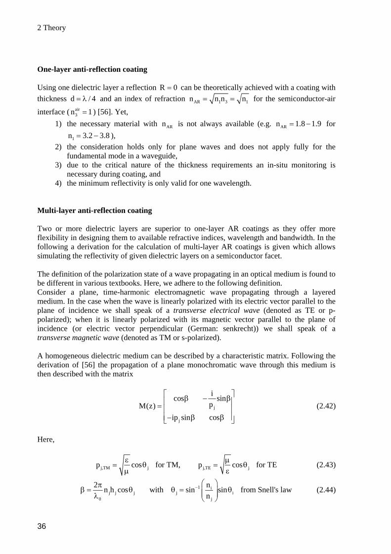
2 Theory
One-layer anti-reflection coating
ielectric layer a reflection R 0Using one d = can be theoretically achieved with a coating with thickness d / 4= λ and an index of refraction AR 1 3n n n= = 1n for the semiconductor-air
terface ) [56]. Yet, th is not always available (e.g. 9 for
8 ),
ndamenature of the thickness requirements an in-situ monitoring is
ecessa ting, and
Mult Two flexib th and bandwidth. In the
llow gimulating the reflectivity of given dielectric layers on a semiconductor facet.
propagating in an optical medium is found to
plane of
( air3n 1=in
1) the necessary material wi ARn ARn 1.8 1.= −
1
2) the consideration holds only for plane waves and does not apply fully for the fu tal mode in a waveguide,
3) due to the critical nn ry during coa
n 3.2 3.= −
4) the minimum reflectivity is only valid for one wavelength.
i-layer anti-reflection coating
or more dielectric layers are superior to one-layer AR coatings as they offer more ility in designing them to available refractive indices, wavelengin a derivation for the calculation of multi-layer AR coatings is given which allows fo
s
he definition of the polarization state of a waveTbe different in various textbooks. Here, we adhere to the following definition. Consider a plane, time-harmonic electromagnetic wave propagating through a layered medium. In the case when the wave is linearly polarized with its electric vector parallel to the plane of incidence we shall speak of a transverse electrical wave (denoted as TE or p-
olarized); when it is linearly polarized with its magnetic vector parallel to thepincidence (or electric vector perpendicular (German: senkrecht)) we shall speak of a transverse magnetic wave (denoted as TM or s-polarized). A homogeneous dielectric medium can be described by a characteristic matrix. Following the derivation of [56] the propagation of a plane monochromatic wave through this medium is then described with the matrix
j
jip sin cos
icos sinpM(z)
⎡ ⎤β − β⎢ ⎥= ⎢ ⎥⎢ ⎥− β β⎣ ⎦
(2.42)
ere, H
j,TM j j,TE jos for TEθ (2.43) p cos for TM, p cε µ= θ =
µ ε
1 ij j j j i
0 j
2 nn h cos with sin sin from Snell's lawn
− ⎛ ⎞πβ = θ θ = θ⎜ ⎟⎜ ⎟λ ⎝ ⎠
(2.44)
36
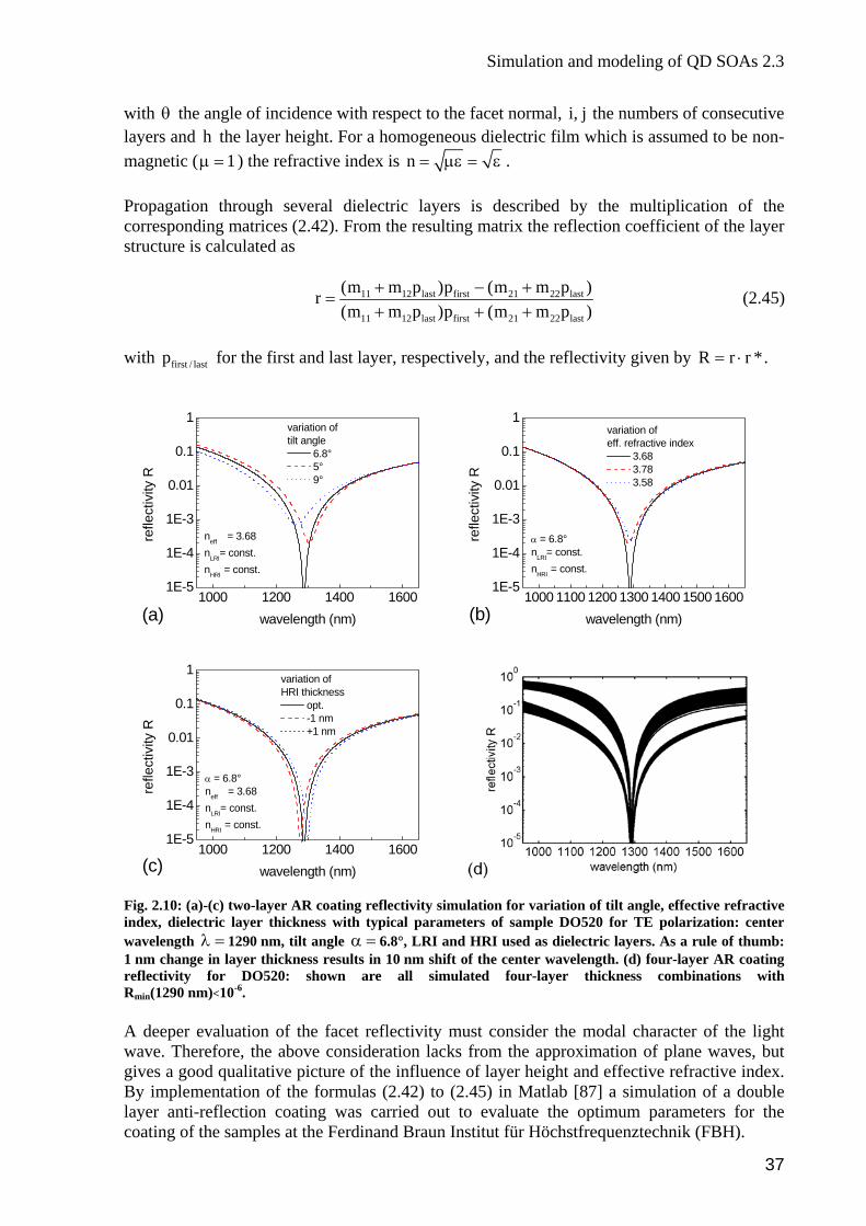
Simulation and modeling of QD SOAs 2.3
with the angle of incidence with respect to the facet normal, the numbers of consecutive yers and the layer height. For a homogeneous dielectric film which is a
magnetic ( ) the refractive index is
θ i, jla ssumed to be non- h
1µ = n = µε = ε . Propagation through several dielectric layers is described by the multiplication of the orresponding matrices (2.42). From the resulting matrix the reflection coefficient of the layer c
structure is calculated as
11 1 21(m mr 2 last first 22 last
11 12 last first 21 22 last
p )p (m m p )(m m p )p (m m p )
+ − ++ + +
(2.45) =
with first / lastp for the first and last layer, respectively, and the reflectivity given by R r r *= ⋅ .
1000 1200 1400 16001E-5
1E-4
1E-3
0.01
0.1
1variation of tilt angle
6.8° 5°
1000 1100 1200 1300 1400 1500 16001E-5
1E-4
1E-3
9°
vity
R
refle
cti
wavelength (nm)
neff = 3.68nLRI= const.nHRI = const.
(a)
0.01
0.1
1
(b)
variation of eff. refractive index
3.68 3.78 3.58
vity
R
refle
cti
wavelength (nm)
α = 6.8°nLRI= const.nHRI = const.
1000 1200 1400 16001E-5
1E-4
1E-3
0.01
0.1
1
(c)
variation of HRI thickness
opt. -1 nm +1 nm
refle
ctiv
ity R
wavelength (nm)
α = 6.8°neff = 3.68nLRI= const.nHRI = const.
Fig. 2.10: (a)-(c) two-layer AR coating reflectivity simulation for variation of tilt angle, effective refractive index, dielectric layer thickness with typical parameters of sample DO520 for TE polarization: center wavelength 1290 nm, tilt angle 6.8°, LRI and HRI used as dielectric layers. As a rule of thumb: 1 nm change in layer thickness results in 10 nm shift of the center wavelength. (d) four-layer AR coating reflectivity for DO520: shown are all simulated four-layer thickness combinations with Rmin(1290 nm)<10-6. A deeper evaluation of the facet reflectivity must consider the modal character of the light wave. Therefore, the above consideration lacks from the approximation of plane waves, but gives a good qualitative picture of the influence of layer height and effective refractive index. By implementation of the formulas (2.42) to (2.45) in Matlab [87] a simulation of a double layer anti-reflection coating was carried out to evaluate the optimum parameters for the coating of the samples at the Ferdinand Braun Institut für Höchstfrequenztechnik (FBH).
λ = α =
37
2 Theory
The FBH considers its AR coatings as intellectual property. Therefore, no details on the coating materials and their layer thicknesses may be published in this thesis. The AR coatings consist of a dielectric two-layer system with a low and a high refracting material. All other details are for internal use only. Here, we will denote the low refractive material with LRI and the material with high refractive index HRI. The effective refractive index of the optical mode in the waveguide is either evaluated theoretically by using an optical mode solver for the lateral structure of the ridge waveguide or it is simply calculated from the optical spectrum of the device from the Fabry-Perot cavity resonances using 2 2= ∆n Lλ λ . Note, if the waveguide is tilted, , the reflectivity of a multilayer AR coating has a strong dependence on the polarization of the mode. The optimization of the layer system can only be done for TE or TM polarization. Fig. 2.10(a-c) shows the dependence of a two layer AR coating for variation of tilt angle, effective refractive index and dielectric layer thicknesses for TE polarization. All parameters have a strong influence on the position and the depth of the minimum reflectivity. This demonstrates how carefully the AR coating has to be designed and experimentally processed. The simulation for a four layer AR coating (Fig. 2.10d) exhibits many combinations of four thicknesses to achieve a minimum reflectivity for the available material combination LRI/HRI/LRI/HRI. We find a bimodal distribution of layer combinations which all achieve reflectivities below 10-6, but show a difference in their bandwidth
0θ >
∆λ ≈ 70 or 20 nm at 10-3. Even the larger bandwidth does not exceed the bandwidth of the two layer AR
coating which is approximately the same at R =
R = 10-3. Therefore, as no improvement is
oat .
indow structure
expected from a four layer coating and due to the costly coating process no experiment with a four layer c ing was conducted Buried facet or w The idea of this approach is to extend the beam waist of the fundamental mode after the waveguide by a window structure with no index guiding in front of the facet. The Gaussian beam waist is
2
2 2 zw (z) w 1⎛ ⎞⎛ ⎞
0 20w⎜ ⎟π⎝ ⎠⎝ ⎠
with dependence on the distance z from the spot size of the beam waist 0w . The extension of the beam waist leads to a reduction of the reflectivity R to
λ⎜ ⎟= + ⎜ ⎟ .46) (2
eff 2 2
RR1 (d w )
=+ λ π
(2.47)
for a length d of cethe buried fa t region [88]. Using typical values ( 0 / nλ = λ = 1.3/3.7 µm,
0.8 µm 0.32) from our structures we find a possible reduction of 6 dB for a window 0
length of 10 µm. But, although a longer region would result in a further decreased reflectivity, the beam would extend and eventually strike the top (metallized) surface of the device,
w = , R =
38
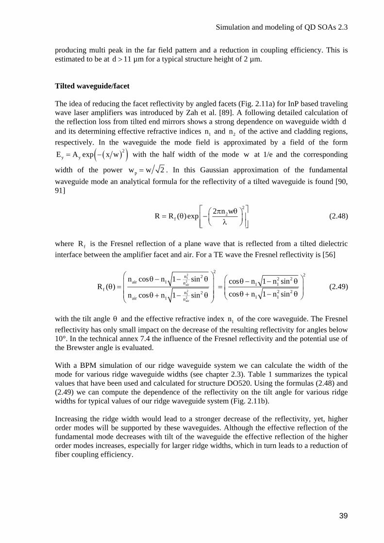
Simulation and modeling of QD SOAs 2.3
producing multi peak in the far field pattern and a reduction in coupling efficiency. This is estimated to be at d > 11 µm for a typical structure height of 2 µm. Tilted waveguide/facet
and
The idea of reducing the facet reflectivity by angled facets (Fig. 2.11a) for InP based traveling wave laser amplifiers was introduced by Zah et al. [89]. A following detailed calculation of the reflection loss from tilted end mirrors shows a strong dependence on waveguide width d
its determining effective refractive indices 1n and 2n of the active and cladding regions, respectively. In the waveguide the mode field is approximated by a field of the form
( )( )2y yE A exp x w= − with the half width of the mode w at 1/e and the corresponding
pw w= 2 oximation of the fundamla for the reflectivity of a tilted waveguide is found [90,
. In this Gaussian appr ental width of the power waveguide mode an analytical formu1] 9
2
22 n wR R ( )expf
⎡ ⎤π θ⎛ ⎞= θ −⎢ ⎥⎜ ⎟λ⎝ ⎠⎢ ⎥⎣ ⎦
here is the Fresnel reflection of a plane wave that isinterface between the amplifier facet and air. For a TE wave the Fresnel reflectivity is [56]
(2.48)
w reflected from a tilted dielectric fR
212air
2
22n 2 2 2
air 1 nf
n
n cos 1 sin cos n 1 nR ( )
⎛ ⎞θ − − θ ⎛ ⎞
12air
1 12 22
1 1air 1 n
n sin
cos n 1 n sinn cos n 1 sin
θ − − θ⎜ ⎟θ = =⎜ ⎟ ⎜ ⎟⎜ ⎟θ + − θ⎜ ⎟θ + − θ ⎝ ⎠⎝ ⎠
(2.49)
with the tilt angle
θ and the effective refractive index of the core waveguide. The Fresnel as
nd the potethe B ngle
ng the formulas (2.48) and .49) we can compute the dependence of the reflectivity on the tilt angle for various ridge idths for typical values of our ridge waveguide system (Fig. 2.11b).
creasing the ridge width would lead to a stronger decrease of the reflectivity, yet, higher
1nreflectivity h only small impact on the decrease of the resulting reflectivity for angles below 10°. In the technical annex 7.4 the influence of the Fresnel reflectivity a ntial use of
rewster a is evaluated. With a BPM simulation of our ridge waveguide system we can calculate the width of the mode for various ridge waveguide widths (see chapter 2.3). Table 1 summarizes the typical values that have been used and calculated for structure DO520. Usi(2w Inorder modes will be supported by these waveguides. Although the effective reflection of the fundamental mode decreases with tilt of the waveguide the effective reflection of the higher order modes increases, especially for larger ridge widths, which in turn leads to a reduction of fiber coupling efficiency.
39
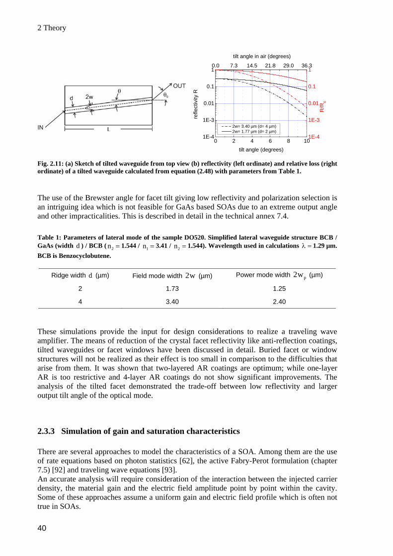
2 Theory
tilt angle in air (degrees)
0 2 4 6 8 101E-4
1E-3
0.01
0.1
1
1E-4
1E-3
0.01
0.1
10.0 7.3 14.5 21.8 29.0 36.3
R/R
refle
0
ctiv
ity R
tilt angle (degrees)
2w= 3.40 µm (d= 4 µm) 2w= 1.77 µm (d= 2 µm)
F ative loss (right ig. 2.11: (a) Sketch of tilted waveguide from top view (b) reflectivity (left ordinate) and relordinate) of a tilted waveguide calculated from equation (2.48) with parameters from Table 1. The use of the Brewster angle for facet tilt giving low reflectivity and polarization selection is an intriguing idea which is not feasible for GaAs based SOAs due to an extreme output angle and other impracticalities. This is described in detail in the technical annex 7.4. Table 1: Parameters of lateral mode of the sample DO520. Simplified lateral waveguide structure BCB / GaAs (width d ) / BCB ( 2n = 1.544 / 1n = 3.41 / 2n = 1.544). Wavelength used in calculations λ = 1.29 µm. BCB is Benzocyclobutene.
Ridge width d (µm) Field mode width 2w (µm) Power m p2wode width (µm)
2 1.73 1.25
4 3.40 2.40
These simulations provide the input for design considerations to realize a traveling wave mplifier. The means of reduction of the crystal facet reflectivity like anti-reflection coatings,
tilted waveguides or facet windows have been discussed in detail. Buried facet or window structures will not be realized as their effect is too small in comparison to the difficulties that arise from them. It was shown that two-layered AR coatings are optimum; while one-layer AR is too restrictive and 4-layer AR coatings do not show significant improvements. The analysis of the tilted facet demonstrated the trade-off between low reflectivity a larger output tilt angle of the optical mode.
2.3.3 Simulation of gain and saturation characteristics There are several approaches to model the characteristics of a SOA. Among them are the use
n accurate analysis will require consideration of the interaction between the injected carrier ensity, the material gain and the electric field amplitude point by point within the cavity.
a
nd
of rate equations based on photon statistics [62], the active Fabry-Perot formulation (chapter 7.5) [92] and traveling wave equations [93]. AdSome of these approaches assume a uniform gain and electric field profile which is often not true in SOAs.
40
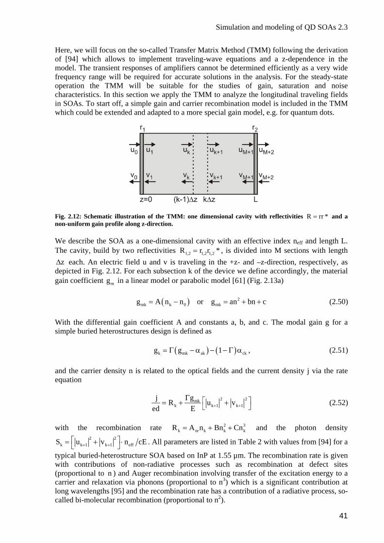
Simulation and modeling of QD SOAs 2.3
Here, we will focus on the so-called Transfer Matrix Method (TMM) following the derivation
tr e p f m required for accurate solutions in the analysis. For the steady-state
will be suitable for the studies of gain, saturation and noise ection we a M alyze aveling fields
in SOAs. To start simp r re thwhich could extended and adapted to re special gain model, e.g. for quantum dots.
of [94] which allows to implement traveling-wave equations and a z-dependence in the model. The ansient r s onses o a plifiers cannot be determined efficiently as a very wide frequency range will be
peration the TMM ocharacteristics. In this s
off, apply the TM to an
le gain and carrie combination mthe longitudinal tr
odel is included in e TMM be a mo
Fig. 2.12: Schematic illustration of the TMM: one dimensional cavity with reflectivities and a
on-uniform gain profile along z-direction.
We describe the SOA as a one-dimensional cavity with an effective index neff and length L.
R rr *=n
The cavity, build by two reflectivities 1,2 1,2 1,2R r r *= , is divided into M sections with length each. An electric field u and v is traveling in the +z- and –z-direction, respectively, as z∆
depicted in Fig. 2.12. For each subsection k of the device we define accordingly, the material gain coefficient mg in a linear model or parabolic model [61] (Fig. 2.13a) ( ) 2
mk k 0 mkg A n n or g an bn c= − = + + (2.50) With the differential gain coefficient A and constants a, b, and c. The modal gain g for a simple buried heterostructures design is defined as ( ) ( )k mk ak ckg g 1= Γ − α − − Γ α , (2.51) and the carrier density n is related to the optical fields and the current density j via the rate equation
2 2mkj gk k 1 k 1R u v
ed E + +Γ ⎡ ⎤= + +⎣ ⎦ (2.52)
with the recombination rate k and the photon density 2 3
k nr k kR A n Bn Cn= + +2 2
k k 1 k 1 effS u v n c+ +⎡ ⎤= + ⋅⎣ ⎦
typical buried-heterostruwith contributions of non-radiative processe(proportional to n ) and Auger recom
E . All parameters are listed in Table 2 with values from [94] for a
cture SOA based on InP at 1.55 µm. The recombination rate is given s such as recombination at defect sites
bination involving transfer of the excitation energy to a carrier and relaxation via phonons (proportional to n3) which is a significant contribution at long wavelengths [95] and the recombination rate has a contribution of a radiative process, so-called bi-molecular recombination (proportional to n2).
41
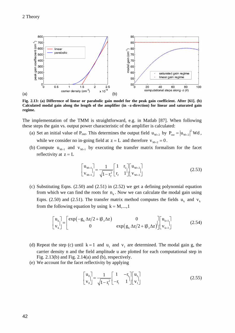
2 Theory
(a) (b)
Fig. 2.13: (a) Difference of linear or parabolic gain model for the peak gain coefficient. After [61]. (b) Calculated modal gain along the length of t in –z-direction) for linear and saturated gain
ime. The implementation of the TMM is straightforward, e.g. in Matlab [87]. When following these steps the gain vs. output power characteristic of the amplifier is calcu
he amplifier (reg
lated: (a) Set an initial value of Pout. This determines the output field 2
out M 2P u Wd+= , M 2u + by z L= and therefore M 2v 0+ = . while we consider no in-going field at
(b) Compute M 1u + and M 1v + by executing the transfer matrix formalism for the facet reflectivity at z L=
M 1 2 M 2
2
M 1 2 M 221 r+ +⎣ ⎦ ⎣ ⎦ ⎣ ⎦
(c) Su
u 1 r u1v r 1 v
+ +⎡ ⎤ ⎡ ⎤ ⎡=⎢ ⎥ ⎢ ⎥ ⎢ ⎥
−
bstituting Eqns. (2.50) and (2.51) in (2.52) we get a defining polynomial equation from which we can find the roots for Now we can calculate the modal gain using Eqns. (2.50) and (2.51). The transfer m trix method cfrom the following equation by using
⎤ (2.53)
kn .a omputes the fields ku and kv
k M,...,1=
(
)( )
k z k 1
k k z k 1
g z 2 i z 0 uv 0 exp g z 2 i z v
+
+
− ∆ + β ∆ ⎡ ⎤⎢ ⎥∆ + β ∆⎣ ⎦ ⎣ ⎦⎣ ⎦
(2.54)
(d) Repeat the step (c) until k 1= and 1u and 1v are determined. The modal gain g, the carrier density n and the field amplitude u are plotted for each computational step in Fig. 2.13(b) and Fig. 2.14(a) and (b), respectively
ku exp⎡ ⎤⎡ ⎤= ⎢ ⎥⎢ ⎥
. (e) We account for the facet reflectivity by applying
0 1 1
20 11
u 1 r1v r 11 r
−⎡ ⎤
1
uv
⎡ ⎤ ⎡ ⎤=⎢ ⎥ ⎢ ⎥ ⎢ ⎥−− ⎣ ⎦ ⎣ ⎦⎣ ⎦
(2.55)
42
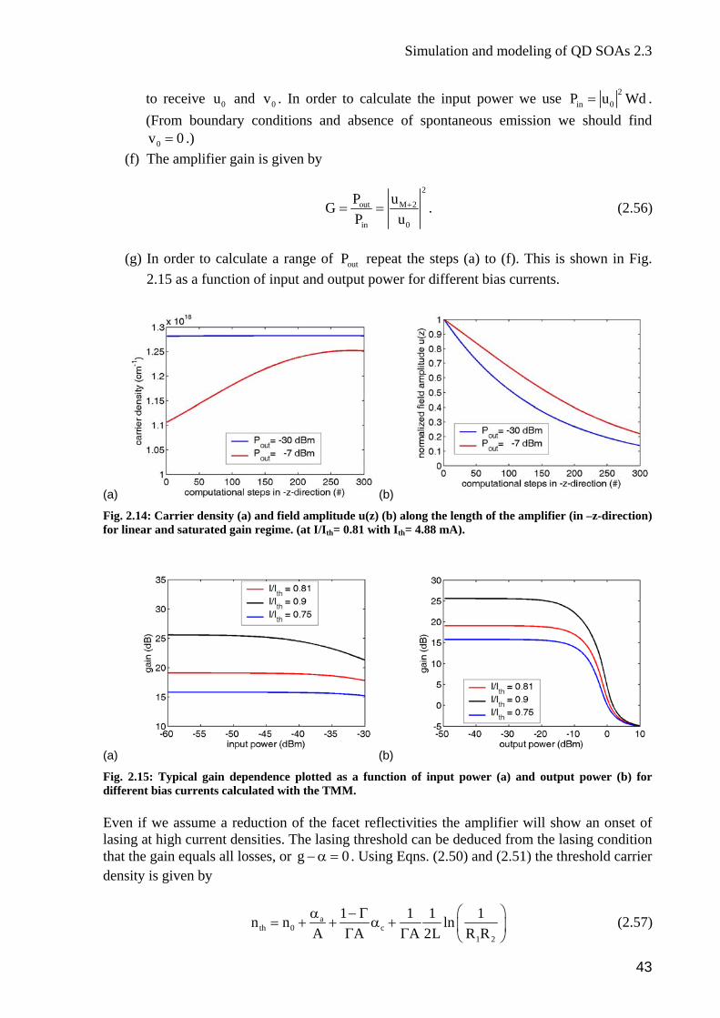
Simulation and modeling of QD SOAs 2.3
to receive nd In order to calculate the input power we use 0u a 0v . 2in 0P u W= should find
d . (From boundary conditions and absence of spontaneous emission we
.) (f) The amplifier gain is given by
0v 0=
2
out M 2
in 0
P uGP u
+= = . (2.56)
(g) In order to calculate a range of repeat the steps (a) to (f). This is shown in Fig.
2.15 as a function of input and output outP
power for different bias currents.
(a) (b)
Fig. 2.14: Carrier density (a) and field amplitude u(z) (b) along the length of the amplifier (in –z-direction) r linear and saturated gain regime. (at I/Ith= 0.81 with Ith= 4.88 mA).
(a)
fo
(b)
puFig. t power (a) and output power (b) for diff
ven if we assume a reduction of the facet reflectivities the sing at high current densities. The lasing threshold can be de
that the gain equals all losses, or
2.15: Typical gain dependence plotted as a function of inerent bias currents calculated with the TMM.
E amplifier will show an onset of la duced from the lasing condition
g 0− α = . Using Eqns. (2.50) and (2.51) the threshold carrier density is given by
a 1 1 1 1n n ln⎛ ⎞α − Γ
= + + α + (2.57) th 0 c1 2A A A 2L R R⎜ ⎟Γ Γ ⎝ ⎠
43

2 Theory
and the threshold current density is found by eq. (2.52) with the photon density assumed to be ero at the lasing threshold (as no spontaneous emission is included in the model).
In this implementation of the model the computational direction is in the minus z-direction. It straightforward – by using inverted matrices – to implement the calculation in +z-direction
wh
he TMM model has several limitations and approximations which are collected here: • the current density is uniform over z which is only true in the approximation of high
serial resistance • no gain compression from thermal effects and renormalization due to high carrier
densities is implemented • no effect of the carrier density on the refractive index which is valid unless the
amplifier is heavily saturated and the carrier density distribution is strongly non-uniform
• no spontaneous emission is considered because its contribution is negligible for gain and saturation characteristics (not for noise) for current densities below the lasing threshold. A detailed formulation of the spontaneous emission with TMM is reported in [96]
• the propagation constant has no modal dependence
ain model (linear or parabolic) that is used
Table 2: Parameters from [94] used in the showcase modeling presented in this section.
Parameter Symbol Value·Unit
z
isich offers the possibility to start with an input power into the SOA.
T
β• although the model is kept rather simple, it is very sensitive on the values of the
parameters and it is already strongly dependent on the g
Facet reflectivity 3.6·10-3
Differential gain coefficient 4.63·10-16 cm2
Transparency carrier density 8.31·10-17 cm-3
Confinement factor
R
A
0n
Γ 0.5
Loss in active waveguide region aα 25 cm-1
ss in cladding region cα Lo 50 cm-1
1.5·10-4 cm
coefficient 7.5·10-29 cm6 s-1
Effective refractive index 3.5
Photon energy
Thickness of active region d 0.2·10-4 cm
Width of active region W
Length of active region L 500·10-4 cm
Non-radiative recombination coefficient nrA 10-8 s-1
Radiative recombination coefficient B 10-10 cm3 s-1
Auger recombination C
effn
E hc= λ 1.28·10-19 J
Wavelength λ 1.55·10 m
Propagation constant
-6
z eff2 nβ = π λ 0.142·106 cm-1
44
Simulation and modeling of QD SOAs 2.3
The way the TMM was described here, it does not work for QDs. The model for material and modal gain must be adapted, and the simple model with the recombination rate (with non- and radiative processes and Auger recombination) is not sufficient to describe the interdependency f barrier, WL, ES and GS of a QD gain medium.
Hercharacteristics like carrier density, modal gain and field amplitude on the z-position along the leng constant while the field amplitude is small at the input and large at the output of the SOA as it is e edisplaypropagation through the amplifier which is also expected due to the increased carrier recombas assusaturaticonsequently also the output poweramplifi mpletely depleted and the net “ga In ordeconsiderable effort would have to be made and all approximations implicit in the model, e.g. a constant current along the device, have to be checked whether they are still valid. The next
roups. T x method was applied to study the ropagation of an o ld through an am al gain and saturation behavior of a SO ated to understand the propagation dependent mechanisms of the carrier density and the modal g
2 dot semiconducto optical amplifi T s it is necessary to develop a detailed theoretical understanding of th e modeling can start off with available informat terial, size a he shape of QDs is often either lens shape or t id like. The m in anc with a large le l of physical de y successfully th plied to calculate the atomlike state QDs and th d piezo-electric fie s on electronic and optical properties of Q I o compute the single- and multi-particl tes, os strength and polarization of optical transitions. These simulations help for instance to umerically the polarization properties of a combined ridge waveguide with the edium, amely quantum dots. For each part of the problem several different approaches are known.
ed by detailed k·p-calculations as it was
o
e we have used the TMM only to describe the general dependency of amplifier
th of the device. It was shown that in the linear regime modal gain and carrier density are
xp cted for the exponentially amplified signal power in the device. The saturated regime s a strong decrease of the modal gain and the carrier density with increasing
ination at larger powers and the direct dependency of the modal gain on carrier density med in this model. Using the complete TMM we were able to simulate the typical gain on for large input powers as it is depicted in Fig. 2.15. As the input power and
is increased, the gain starts to saturate and eventually the er is forced towards transparency where the gain is co
in” is completely determined by the total waveguide loss.
r to apply this model to simulate QD amplifiers and explain and predict their behavior
section introduces the modeling of QD SOAs as it is done with extensive man power by other g
he transfer matri p ptical fieplifier. In this modeling the gener A was illustr
ain along the device.
.3.4 Modeling of quantum r ers
o model QD based SOAe QD properties. Th ion like ma
nd shape of the QDs. T runcated pyramodeling of the individual QD wavefunction, eigenenergy, stra
an be done with numerical methods d piezo-electric fields
tail. Vervee 8-band k·p method has been ap spectrum ofe influence of shape, strain an ldDs [75, 97-99].
t is possible t e sta cillation simulate n
active gain mnThe polarization properties of a ridge waveguide are often tackled with a mode solver for the cross section of the device and a beam propagation method to describe the propagation of the mode(s) through the waveguide. The polarization properties of the gain medium are mainly determined by the recombination probabilities of the involved excitons and their fraction of
H- and LH-contribution. This can be computH
45
2 Theory
described in section 2.2.6. On the whole we seek for a numerical solution which combines the various effects on the polarization of the amplified light from the waveguide and the gain medium. Ideally we would like to have a tool that predicts
• the TE/TM polarization fraction of the light output from the complete device or • the polarization dependent gain of the SOA
subject to ridge waveguide dimensions and composition as well as QD parameters like stacking distance, strain, Indium content and the like.
Such a complete simulation tool is not available to date and could not be developed in the framework of this project. A reduction of the complexity in modeling of the QD gain medium can be achieved by the use of phenomenological key parameters like single dot gain, volume, confinement energy, and capture times, averaged over the QD ensemble. For such a modeling of QD devices a rate quation approach is widely used ranging from rather simple models to more complex models
heoretically many device properties have been predicted that fuel the interest in QD SOAs
the QD gain and an implementation of this active medium in SOAs onsidering ASE, cw and dynamic processes with a multi population rate equation model is
ra et al. ng by QD SOAs
04]. The linear optical response as well as the incoherent and coherent nonlinear response of
ected. Pattern-effect-free wavelength conversion by XGM with low equency chirping and symmetric highly-efficient 1 to 2 THz wavelength conversion by the
ics [45]. The interplay of ferent uni mpared with conventional devices based
e[59, 86, 100-105]. Alternatively, the master equation approach [22, 106, 107] or the use of Bloch equations [108] can be applied. These models are able to include the position dependence within the device with a stepwise calculation similar to the TMM approach introduced in section 2.3.3. Tand promise excellent performance of these amplifiers. Some of these theoretical findings are reviewed here without intending to be exhaustive. Full scale modeling of cpresented in detail in the thesis of Berg [59]. A comprehensive paper of Sugawadevelops and displays a theory of optical signal amplification and processi[1the devices with arbitrary spectral and spatial distribution of quantum dots in the active region are calculated. The incoherent nonlinear response is due to the incoherent spectral hole burning and the reduction in the carrier density by the stimulated emission, while the coherent nonlinearity is due to the dynamic spectral hole burning caused by the population beating at the electronic states resonant to the multimode light and the carrier density pulsation caused by the carrier relaxation dynamics. From the QD SOAs low power consumption, high saturation power, broad gain bandwidth, and pattern-effect-free operation under gain saturation is expfrnon-degenerate FWM is predicted for signal processing devices which realize high speed of 40 to 160 Gb/s. For the high-speed optical signal processing the nonlinear optical response due to the spectral hole burning has the main effect on the amplifier performance. The findings of this paper are supported by various results that have been published before and after it. The ultrafast gain recovery of QDs is explained by a comprehensive numerical model where the QD excited state carriers are found to act as a reservoir for the optically active ground state carriers resulting in an ultrafast gain recovery as long as the excited state is well populated. But modulation limitations in the self-assembled quantum-dot devices when pulses are injected into the device at high-repetition frequencies are predicted because the response of the QD amplifiers is found to be limited by the wetting-layer dynam
the carrier reservoir for the QDs and the fast carrier relaxation gives rise for difque properties of the quantum dot based SOAs co
46

Simulation and modeling of QD SOAs 2.3
on bulki.e. wit d fast nonlinearities by breaking
carrier depletion can be eliminated by increasing the SOA pump urrent density. At high pump currents, gain saturation in QD SOAs is then due to spectral
escape from the ground state significantly affects the performance f the amplifier. The small-signal cross gain conversion efficiency shows strong dependence
gain modulation by change of the photon ensity which is possible due to the spectral hole burning effects in the regime with maximum
rate patterned optical signals, which meet with the demand of next-generation roadband all-optical photonic networks are promised [113]. With interferometers containing
or quantum well material. QD devices may be operated in regimes of high linearity, h a high saturation power, but can also show strong an
the equilibrium between discrete dot states and the continuum of wetting layer states [109]. The gain saturation due to chole burning. As a result, the saturation power for cw amplification can be enhanced by two orders in magnitude in QD SOAs [53]. Qasaimeh describes wavelength conversion based on four-wave mixing and cross gain conversion in quantum dot semiconductor optical amplifiers. The model takes into account the effect of the multidiscrete QD energy levels and the wetting layer. The high FWM conversion efficiencies at high detuning frequency are attributed to the discreteness of the energy levels, where carrier oon the escape and relaxation lifetimes between the ground and excited states [110, 111]. Uskov et al. model QD SOAs which allow for high-speed cross-gain modulation without pattern effects. This is attributed to instantaneous dlinear gain. The maximum bit-rate at modulation bit-rates much higher than the interband relaxation rate for this pattern-effect free XGM grows with increasing pump current density of the QD SOA [37]. Bilenca and Eisenstein describe the XGM via the noise properties of linear and nonlinear QD amplifiers by considering the impact of the inhomogeneously broadened gain and the fast carrier dynamics under a saturating signal. The optical noise spectrum at the amplifier output comprises broad-band ASE which in saturation contains an added spectral hole due to a nonlinear noise-signal interaction. This spectral hole stems from saturation of the inhomogeneously broadened gain and the narrower portion is due to a distributed nonlinear interaction between the saturating signal propagating down the amplifier axis and the amplifier noise. The most important characteristics of the optical and electrical noise spectra are determined by the degree of inhomogeneous broadening and by the fast carrier dynamics of QD amplifiers. The fast dynamics causes a very wide noise spectral hole which has important potential consequences for all optical signal processing [112]. 40-Gbit/s dynamic performance of QD amplifiers was calculated and compared with bulk SOAs. The results demonstrate that quantum dot SOAs can process multiple-wavelength high bit-rate optical pulse trains over 40 Gbit/s under gain saturation. Functions like regeneration, reshaping, multiple-wavelength processing, wavelength conversion, and demultiplexing of high-bit-bquantum dot SOAs ultrafast cross phase modulation and digital signal processing with low dependence on the specific random data pattern is possible [114]. Furthermore, high-bit-rate signal processing up to 160 Gb/s and a new scheme of 3R regenerator are envisioned based on the spectral hole burning properties of the inhomogeneously broadened QD ensemble and its unique gain saturation character. The theory includes spatial isolation of quantum dots, carrier relaxation and excitation among the discrete energy states and the wetting layer, grouping of dots by their optical resonant frequency under the inhomogeneous broadening, and the homogeneous broadening of the single-dot gain, which are all essential to the amplifier performance. Switching functions can be realized by the cross gain modulation between two wavelength channels when the channel separation is within the homogeneous broadening, allowing the possible application of a quantum dot based 3R (re-amplification, re-shaping, re-timing) regenerator [115].
47

2 Theory
It is beyond the scope of this thesis to im mple ent a full scale modeling of QD SOAs. This last art of the theory chapter has given a review on available models for QD amplifiers and has p
subsumed important results that predict excellent performance of QD based SOAs in comparison to conventional SOAs.
48
Growth of quantum dots 3.1
3 Processing and Fabrication
.1 Growth of quantum dots
he idea and advantages of using QDs as an active medium have been described in the introduction and section 2.1. The growth of quantum dots is a broad field [23] and will be only briefly summarized in this thesis. In general we would like to make use of QDs as a gain medium for SOAs in order to achieve an emission wavelength of 1.3 µm based on a GaAs substrate, realize a moderate gain comparable to QW devices, attain a broad wavelength bandwidth and improve the dynamic properties of SOAs. For the growth of semiconductor material in general, several growth techniques exist. Most commonly the structures are grown by molecular beam epitaxy (MBE) [116] and metal organic chemical vapor deposition (MOCVD) [117, 118]. Using MOCVD, established as commercial large-scale fabrication technology for electronic and optoelectronic semiconductor devices in Europe, very high deposition rates can be achieved, and since no UHV is needed like in MBE a larger throughput is yielded. But MOCVD growth is rather difficult to control as the reactants are supplied as organic or hydride precursors that are thermally cracked by the heated substrate susceptor making the fraction of reactants in the gas phase a function of temperature. The choice of precursor molecules, total pressure and total gas flow are additional parameters that have to be controlled in contrast to MBE. In MBE, growth conditions can very accurately be defined, controlled, and monitored. The reactants can be supplied in elemental form by molecular beams that are directed perpendicularly onto a heated substrate placed in a UHV chamber. The growth process is controlled by substrate temperature and molecular flows only. In-situ monitoring of the growth is available with reflection high-energy electron diffraction (RHEED). Although QD self-organization has been investigated using both, MOCVD and MBE, the samples used for measurements in this thesis were grown by MBE as they were the only available samples with emission wavelength in the 1.26 – 1.31 µm regime. The methods to fabricate nanostructures with size dimensions below the DeBroglie wavelength and to achieve an electronic confinement in three dimensions can be divided into three categories [20]. 1) The inclusion of nano-sized semiconductor material (often CdS and CdSe) in a glass matrix leads to a quantum dot material class that is frequently used for color filters8. The QDs in a glass matrix are usually surrounded by an isolating material, therefore, these QDs can not be deployed easily in opto-electronic functions. They are sometimes used to characterize the properties of single dots. 2) Lithography, substrate patterning and etching techniques build the second category which allow to tailor the shape and size of QDs with the help of e-beam lithography [119]. Although the idea of having full control on the formation of the nanostructures is intriguing and highly desirable for many applications the etching processes often cause roughness and damage to the crystalline structure of the QD semiconductor material. This fact and also the difficulties in having a large scale production of these kind of QDs on a full wafer by the use of e-beam lithography have narrowed down the use of this tailor-made QDs. 3) So-called self-assembled or self-organized QDs have proven to be the most versatile and reliably grown nanostructures used for opto-electronic devices. Island like growth is distinguished by the associated surface strain energies into Frank-van-der-Merve growth
3 T
8 One of the earliest applications of nanotechnology (without people actually knowing it was nanotechnology), was the use of nanoparticles in red church windows.
49
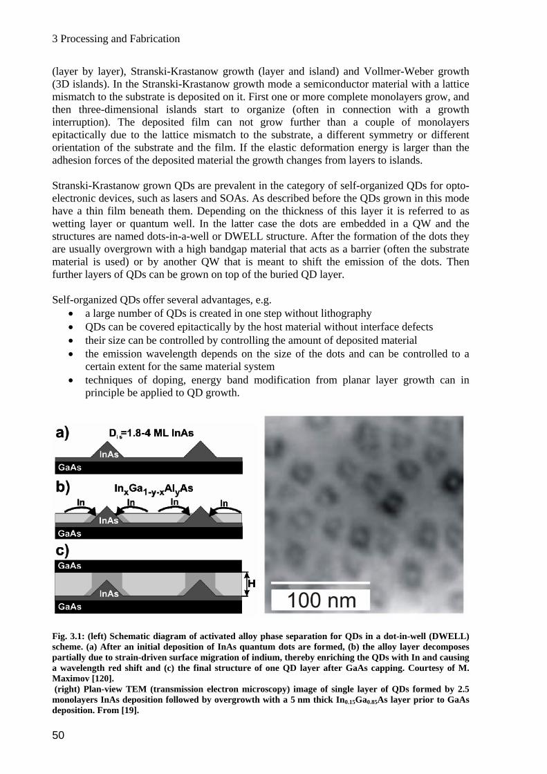
3 Processing and Fabrication
(layer by layer), Stranski-Krastanow growth (layer a(3D islands). In the Stranski-Krastanow growth mode
nd island) and Vollmer-Weber growth a semiconductor material with a lattice
atch to the substrate is deposited on it. First one or more complete monolayers grow, and rganize (often in connection with a growth
terruption). The deposited film can not grow further than a couple of monolayers
before the QDs grown in this mode ave a thin film beneath them. Depending on the thickness of this layer it is referred to as
mismthen three-dimensional islands start to oinepitactically due to the lattice mismatch to the substrate, a different symmetry or different orientation of the substrate and the film. If the elastic deformation energy is larger than the adhesion forces of the deposited material the growth changes from layers to islands. Stranski-Krastanow grown QDs are prevalent in the category of self-organized QDs for opto-electronic devices, such as lasers and SOAs. As described hwetting layer or quantum well. In the latter case the dots are embedded in a QW and the structures are named dots-in-a-well or DWELL structure. After the formation of the dots they are usually overgrown with a high bandgap material that acts as a barrier (often the substrate material is used) or by another QW that is meant to shift the emission of the dots. Then further layers of QDs can be grown on top of the buried QD layer. Self-organized QDs offer several advantages, e.g.
• a large number of QDs is created in one step without lithography • QDs can be covered epitactically by the host material without interface defects • their size can be controlled by controlling the amount of deposited material • the emission wavelength depends on the size of the dots and can be controlled to a
certain extent for the same material system • techniques of doping, energy band modification from planar layer growth can in
principle be applied to QD growth.
Fig. 3.1: (left) Schematic diagram of activated alloy phase separation for QDs in a dot-in-well (DWELL) scheme. (a) After an initial deposition of InAs quantum dots are formed, (b) the alloy layer decomposes partially due to strain-driven surface migration of indium, thereby enriching the QDs with In and causing a wavelength red shift and (c) the final structure of one QD layer after GaAs capping. Courtesy of M. Maximov [120].
sion electron microscopy) image of single layer of QDs formed by 2.5 (right) Plan-view TEM (transmismonolayers InAs deposition followed by overgrowth with a 5 nm thick In0.15Ga0.85As layer prior to GaAs deposition. From [19].
50
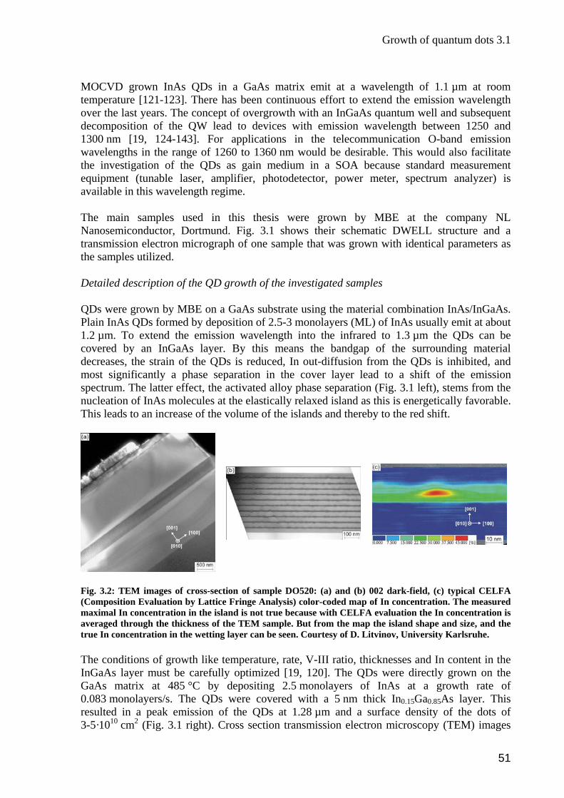
Growth of quantum dots 3.1
MOCVD grown InAs QDs in a GaAs matrix emit at a wavelength of 1.1 µm at room temperature [121-123]. There has been continuous effort to extend the emission wavelength over the last years. The concept of overgrowth with an InGaAs quantum well and subsequent decomposition of the QW lead to devices with emission wavelength between 1250 and 1300 nm [19, 124-143]. For applications in the telecommunication O-band emission wavelengths in the range of 1260 to 1360 nm would be desirable. This would also facilitate the investigation of the QDs as gain medium in a SOA because standard measurement quipment (tunable laser, amplifier, photodetector, power meter, spectrum analyzer) is
ing the material combination InAs/InGaAs. Pla n usually emit at about 1.2 can be cov d material dec smost s er layer lead to a shift of the emission spe unucleat
his lea nds and thereby to the red shift.
eavailable in this wavelength regime. The main samples used in this thesis were grown by MBE at the company NL Nanosemiconductor, Dortmund. Fig. 3.1 shows their schematic DWELL structure and a transmission electron micrograph of one sample that was grown with identical parameters as the samples utilized. Detailed description of the QD growth of the investigated samples QDs were grown by MBE on a GaAs substrate us
in I As QDs formed by deposition of 2.5-3 monolayers (ML) of InAs µm. To extend the emission wavelength into the infrared to 1.3 µm the QDs ere by an InGaAs layer. By this means the bandgap of the surroundingrea es, the strain of the QDs is reduced, In out-diffusion from the QDs is inhibited, and
ignificantly a phase separation in the covctr m. The latter effect, the activated alloy phase separation (Fig. 3.1 left), stems from the
ion of InAs molecules at the elastically relaxed island as this is energetically favorable. ds to an increase of the volume of the islaT
Fig. 3.2: TEM images of cross-section of sample DO520: (a) and (b) 002 dark-field, (c) typical CELFA (Composition Evaluation by Lattice Fringe Analysis) color-coded map of In concentration. The measured maximal In concentration in the island is not true because with CELFA evaluation the In concentration is averaged through the thickness of the TEM sample. But from the map the island shape and size, and the
n concentration in the wetting layer can be seen. Courtesy of D. Litvinov, University Karlsruhe.
rs/s. The QDs were covered with a 5 nm thick In0.15Ga0.85As layer. This
true I The conditions of growth like temperature, rate, V-III ratio, thicknesses and In content in the InGaAs layer must be carefully optimized [19, 120]. The QDs were directly grown on the GaAs matrix at 485 °C by depositing 2.5 monolayers of InAs at a growth rate of 0.083 monolayeresulted in a peak emission of the QDs at 1.28 µm and a surface density of the dots of 3-5·1010 cm2 (Fig. 3.1 right). Cross section transmission electron microscopy (TEM) images
51
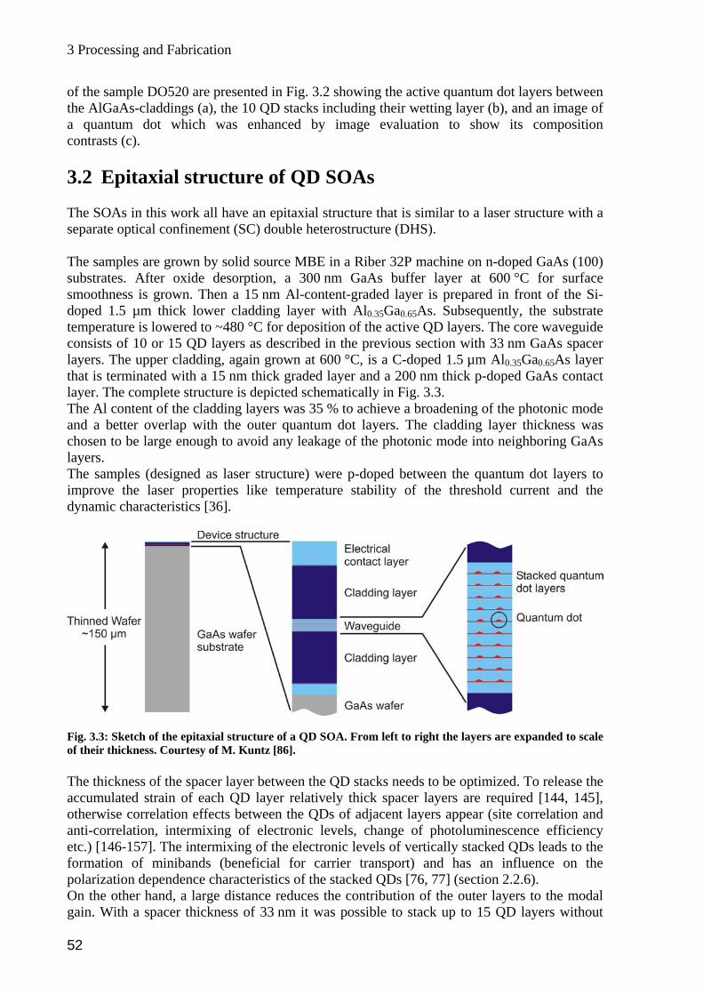
3 Processing and Fabrication
of the sample DO520 are presented in Fig. 3.2 showing the active quantum dot layers between
to ~480 °C for deposition of the active QD layers. The core waveguide with 33 nm GaAs spacer .5 µm Al0.35Ga0.65As layer
the AlGaAs-claddings (a), the 10 QD stacks including their wetting layer (b), and an image of a quantum dot which was enhanced by image evaluation to show its composition contrasts (c). 3.2 Epitaxial structure of QD SOAs The SOAs in this work all have an epitaxial structure that is similar to a laser structure with a separate optical confinement (SC) double heterostructure (DHS). The samples are grown by solid source MBE in a Riber 32P machine on n-doped GaAs (100) substrates. After oxide desorption, a 300 nm GaAs buffer layer at 600 °C for surface smoothness is grown. Then a 15 nm Al-content-graded layer is prepared in front of the Si-doped 1.5 µm thick lower cladding layer with Al0.35Ga0.65As. Subsequently, the substrate emperature is loweredt
consists of 10 or 15 QD layers as described in the previous sectionayers. The upper cladding, again grown at 600 °C, is a C-doped 1l
that is terminated with a 15 nm thick graded layer and a 200 nm thick p-doped GaAs contact layer. The complete structure is depicted schematically in Fig. 3.3. The Al content of the cladding layers was 35 % to achieve a broadening of the photonic mode and a better overlap with the outer quantum dot layers. The cladding layer thickness was chosen to be large enough to avoid any leakage of the photonic mode into neighboring GaAs layers. The samples (designed as laser structure) were p-doped between the quantum dot layers to improve the laser properties like temperature stability of the threshold current and the dynamic characteristics [36].
Fig. 3.3: Sketch of the epitaxial structure of a QD SOA. From left to right the layers are expanded to scale of their thickness. Courtesy of M. Kuntz [86]. The thickness of the spacer layer between the QD stacks needs to be optimized. To release the ccumulated strain of each QD layer relatively thick spacer layers are required [144, 14a 5],
otherwise correlation effects between the QDs of adjacent layers appear (site correlation and anti-correlation, intermixing of electronic levels, change of photoluminescence efficiency etc.) [146-157]. The intermixing of the electronic levels of vertically stacked QDs leads to the formation of minibands (beneficial for carrier transport) and has an influence on the polarization dependence characteristics of the stacked QDs [76, 77] (section 2.2.6). On the other hand, a large distance reduces the contribution of the outer layers to the modal gain. With a spacer thickness of 33 nm it was possible to stack up to 15 QD layers without
52
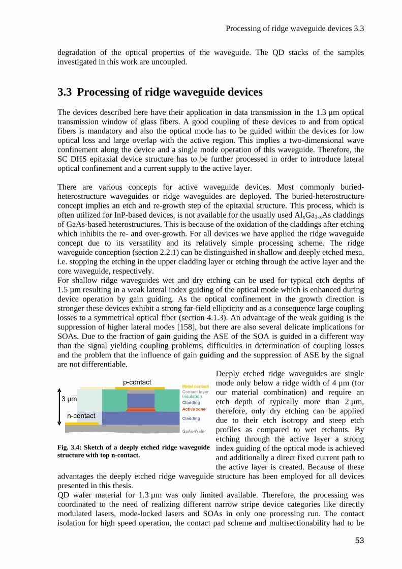
Processing of ridge waveguide devices 3.3
degradation of the optical properties of the waveguide. The QD stacks of the samples investigated in this work are uncoupled. 3.3 Processing of ridge waveguide devices
he devices described here have their application in data transmission in the 1.3 µm optical
within the devices for low ptical loss and large overlap with the active region. This implies a two-dimensional wave
the claddings after etching
ping the etching in the upper cladding layer or etching through the active layer and the
ral index guiding of the optical mode which is enhanced during evice operation by gain guiding. As the optical confinement in the growth direction is
stronger these devices exhibit a strong far-field ellipticity and as a consequence large coupling losses to a symmetrical optical fiber (section 4.1.3). An advantage of the weak guiding is the suppression of higher lateral modes [158], but there are also several delicate implications for SOAs. Due to the fraction of gain guiding the ASE of the SOA is guided in a different way than the signal yielding coupling problems, difficulties in determination of coupling losses and the problem that the influence of gain guiding and the suppression of ASE by the signal are not differentiable.
Deeply etched ridge waveguides are single mode only below a ridge width of 4 µm (for our material combination) and require an etch depth of typically more than 2 µm,therefore, only dry etching can be applied
profiles as compared to wet etchants. By etching through the active layer a strong
ectly
Ttransmission window of glass fibers. A good coupling of these devices to and from optical fibers is mandatory and also the optical mode has to be guided oconfinement along the device and a single mode operation of this waveguide. Therefore, the SC DHS epitaxial device structure has to be further processed in order to introduce lateral optical confinement and a current supply to the active layer. There are various concepts for active waveguide devices. Most commonly buried-heterostructure waveguides or ridge waveguides are deployed. The buried-heterostructure concept implies an etch and re-growth step of the epitaxial structure. This process, which is often utilized for InP-based devices, is not available for the usually used AlxGa1-xAs claddings of GaAs-based heterostructures. This is because of the oxidation of which inhibits the re- and over-growth. For all devices we have applied the ridge waveguide concept due to its versatility and its relatively simple processing scheme. The ridge waveguide conception (section 2.2.1) can be distinguished in shallow and deeply etched mesa, i.e. stopcore waveguide, respectively. For shallow ridge waveguides wet and dry etching can be used for typical etch depths of 1.5 µm resulting in a weak lated
due to their etch isotropy and steep etch
index guiding of the optical mode is achieved and additionally a direct fixed current path to the active layer is created. Because of these
advantages the deeply etched ridge waveguide structure has been employed for all devices presented in this thesis. QD wafer material for 1.3 µm was only limited available. Therefore, the processing was coordinated to the need of realizing different narrow stripe device categories like dir
Fig. 3.4: Sketch of a deeply etched ridge waveguide structure with top n-contact.
modulated lasers, mode-locked lasers and SOAs in only one processing run. The contact isolation for high speed operation, the contact pad scheme and multisectionability had to be
53
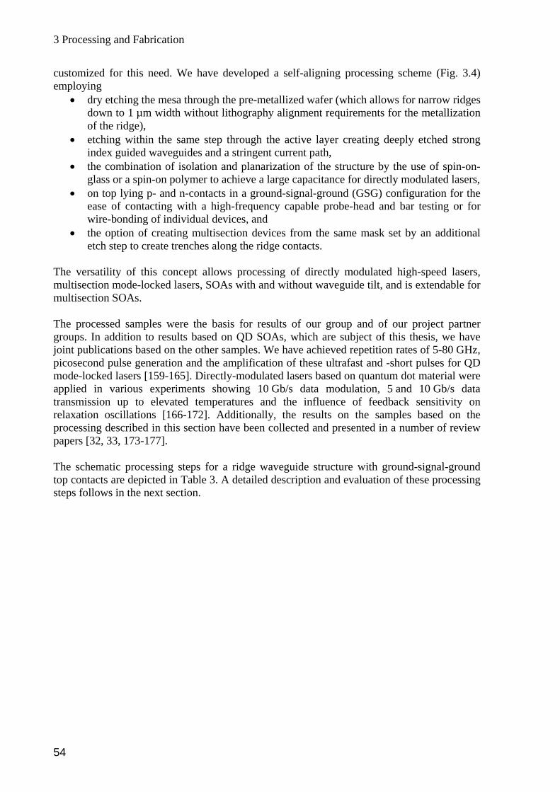
3 Processing and Fabrication
customized for this need. We have developed a self-aligning processing scheme (Fig. 3.4) employing
• dry etching the mesa through the pre-metallized wafer (which allows for narrow ridges down to 1 µm width without lithography alignment requirements for the metallization
same mask set by an additional etch step to create trenches along the ridge contacts.
Directly-modulated lasers based on quantum dot material were
of the ridge), • etching within the same step through the active layer creating deeply etched strong
index guided waveguides and a stringent current path, • the combination of isolation and planarization of the structure by the use of spin-on-
glass or a spin-on polymer to achieve a large capacitance for directly modulated lasers, • on top lying p- and n-contacts in a ground-signal-ground (GSG) configuration for the
ease of contacting with a high-frequency capable probe-head and bar testing or for wire-bonding of individual devices, and
• the option of creating multisection devices from the
The versatility of this concept allows processing of directly modulated high-speed lasers, multisection mode-locked lasers, SOAs with and without waveguide tilt, and is extendable for multisection SOAs. The processed samples were the basis for results of our group and of our project partner groups. In addition to results based on QD SOAs, which are subject of this thesis, we have joint publications based on the other samples. We have achieved repetition rates of 5-80 GHz, picosecond pulse generation and the amplification of these ultrafast and -short pulses for QD mode-locked lasers [159-165]. applied in various experiments showing 10 Gb/s data modulation, 5 and 10 Gb/s data transmission up to elevated temperatures and the influence of feedback sensitivity on relaxation oscillations [166-172]. Additionally, the results on the samples based on the processing described in this section have been collected and presented in a number of review papers [32, 33, 173-177]. The schematic processing steps for a ridge waveguide structure with ground-signal-ground top contacts are depicted in Table 3. A detailed description and evaluation of these processing steps follows in the next section.
54
Processing of ridge waveguide devices 3.3
Table 3: Schematic processing steps for ridge waveguide structure with top n-contacts
. Process description Mask layout Cross section of wafer No
1
Tppt
he wafer is grown by MBE as described reviously. In general only a part of the wafer is rocessed. First, the wafer surface is cleaned
horoughly. mask set
2 Awt
metal contact is evaporated on top of the afer to provide a contact to the ridges without
he need of mask alignment.
3 The first lithography step defines the mesa structure for the ridge waveguides.
4 cladding and the core waveguide, the deeply etched ridge waveguide is formed.
By dry etching through the metal layer, the top
5 An insulation step provides electrical insulation, passivation of the ridge edges and additional planarization of the structure.
6 Dry etching reduces the overall height of the insulation and uncovers the ridge contacts.
7
This lithography step is followed by dry etching to open the n-layer and to remove the insulator on that part of the wafer that will be scribed and broken.
8 Another negative lithography defines the top contacts and the metal is evaporated on the n-layer.
9 This final negative lithography prepares the bond pads which extend the ridge contacts. Then metal evaporation and sputtering follows.
10
The completed top structure consists of a deeply etched ridge waveguide with a ground-signal-ground (GSG) contact pad design. Further processing and fabrication steps follow.
55
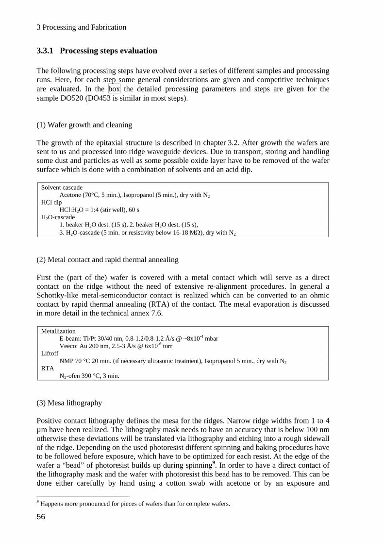
3 Processing and Fabrication
3.3.1 Processing steps evaluation T llowing proc lved over a se ifferent samples and processing runs. H derations are given and competitive techniques are ev parameters and steps are given for the
he fo essing steps have evo ries of dere, for each step some general consi
aluated. In the box the detailed processingsa le (1) Wafer growth and cleaning T gr in chap r 3.2. After growth the wafers are sent to us and processed into transport, storing and handling some dust and particles as well as some possible oxide layer have to be removed of the wafer surface which is done with a combination of solvents and an acid dip.
Solve
mp DO520 (DO453 is similar in most steps).
he owth of the epitaxial structure is described ridge waveguide devices. Due to
te
nt cascade Acetone (70°C, 5 min.), Isopropanol (5 min.), dry with N2
HCl dip HCl:H2O = 1:4 (stir well), 60 s
H -c2O ascade 1. beaker H2O dest. (15 s), 2. beaker H O dest. (152 s), 3. H O-cascade (5 min. or resistivity b2 elow 16-18 MΩ), dry with N2
(2 e First the (part of the) wafer is covered with a metal contact which will serve as a direct contact on the ridge without the need of extensive re-alignment procedures. In general a Schott alized which can be converted to an ohmic co ac e contact. The metal evaporation is discussed in more detail in the technical annex 7.6.
Metal
) M tal contact and rapid thermal annealing
ky-like metal-semiconductor contact is ret by rapid thermal annealing (RTA) of thnt
lization E-beam: Ti/Pt 30/40 nm, 0.8-1.2/0.8-1.2 Å/s @ ~8x10⁻⁴ mbar Veeco: Au 200 nm, 2.5-3 Å/s @ 6x10⁻⁶ torr
Liftoff NMP 70 °C 20 min. (if necessary ultrasonic treatment), Isopropanol 5 min., dry with N2
RTA N2-ofen 390 °C, 3 min.
(3) Mesa lithography Po tiv r the ridges. Narrow ridge widths from 1 to 4 µm ha s to have an accuracy that is below 100 nm otherwise these deviations will be translated via lithography and etching into a rough sidewall of the ridge. Depending on the used photoresist different spinning and baking procedures have to be followed before exposure, which have to be optimized for each resist. At the edge of the w r pinning9. In order to have a direct contact of the lith resist this bead has to be removed. This can be done either carefully by hand using a cotton swab with acetone or by an exposure and
si
e contact lithography defines the mesa fove been realized. The lithography mask need
afe a “bead” of photoresist builds up during sography mask and the wafer with photo
ppens more pronounced for pieces of wafers than for complete wafers. 9 Ha
56
Processing of ridge waveguide devices 3.3
development step of the wafer edge while covering the center. After baking the wafer
/cm2 power. Then the resist is developed, possibly baked and cleaned with a soft oxide plasma.
ture of 2/2 and 4/4 µm double ridges (see Fig. 3.10). Results on the
d characteristics of various ridge widths and etch depths are presented in section 4.1.
Positiv
should rest for a couple of minutes to allow the photoresist to resorb water from air humidity. It is exposed with a Suess MA6 mask aligner at 320 nm wavelength and 6 mW
Ridge widths of 1, 1.5, 2, 4, 8 and 10 µm have been successfully fabricated in various process runs. Due to reasons of yield and single mode operation the mask diversity has been reduced to a tex
Fig. 3.5: Microscope picture of positive lithography fo e ridges with 2 µm (left) and 4 µm r definition of th(right). In the middle the alignment mark is shown far fielwith feature sizes on the order of one micrometer.
e lithography AZ701MIR HCl dip 120s, solvent cascade, prebake 5 min. 120°, spin MA-P 1250 rpm 30 s, bake 2 min. 100°
Edge removal: expose 40 s, develop AZ351B:H2O (1:4) 30 s Mesa litho: expose 20 s, develop AZ351B:H O (1:4) 45 s, plasma P2 5 min. 150 W 2
XP2 profiler: resist height ~1100 nm (4) Etching of mesa For the definition of the narrow mesa structures wet and dry etching can be applied. Early samples were wet etched shallowly, i.e. the process was stopped within the upper cladding
yer. Depending on the etchant mixture, the process has a more or less pronounced lateral e whic auses the sidewalls of the mesa to become tilted and rough. Wet etching below 4 µm and for etch depths largeD ith high a assisted ion beam d reactive ion etching (RIE). By this means the self-aligned rocessing scheme could be implemented as it is possible to etch through the top metal layer ith CAIBE. The dry etching process with an Oxford Plasma Ionfab 300 Plus CAIBE system
il in [178]. In principle, accelerated Ar ions provide the mechanical otropic sputtering part of this etching process and Cl2 is the chemical component which
source and extracted into the ion beam. The process that results is partially chemical, as the n products are sputtered away
latch component h c
is difficult and unstable to control for ridge widthsr t
ry etchan 2 µm. hing provides a powerful tool to achieve vertical and smooth sidewalls w
tios. Therefore, the processing was adjusted to the use of chemically spect raetching (CAIBE) an
pwwas described in detaisetches anisotropic and selectively. By adjusting the two components smooth etch profiles with little surface damage and a high semiconductor-photoresist selectivity can be achieved. CAIBE is used to etch the top metallization and the (Al)GaAs semiconductor layers. The plasma etching system Sentech SI 591 provides a versatile etch process in which argon ions are generated inside the ion source and are accelerated into a broad parallel beam, and to a defined energy, by the extraction grids on the front of the source. If one uses an inert gas such as argon, the process is relatively slow, and the heat that is generated must be removed with care. With a RF ion source gases such as Cl2, F2, CF4, and O2 are cracked in the ion
ions react with the surface, and partially physical, as the reactio
57
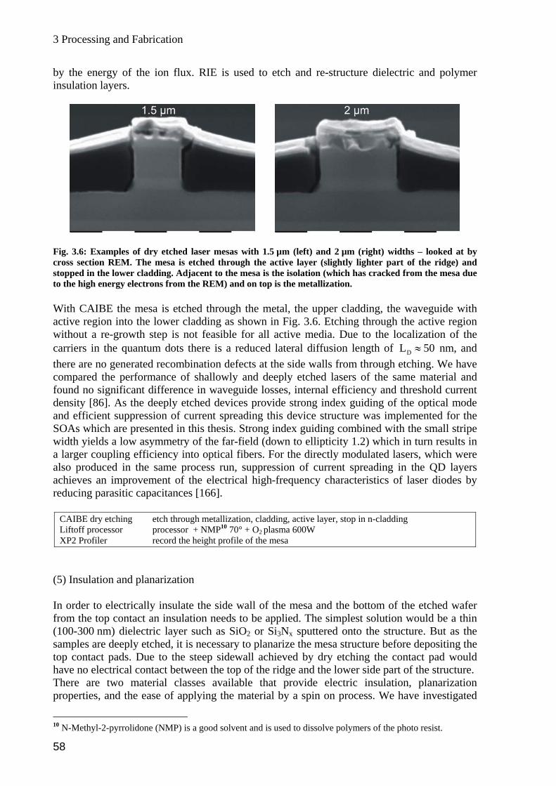
3 Processing and Fabrication
by the energy of the ion flux. RIE is used to etch ainsulation layers.
nd re-structure dielectric and polymer
eft) and 2 µm (right) widths – looked at by layer (slightly lighter part of the ridge) and lation (which has cracked from the mesa due metallization.
With CAIBE the mesa is etched through the metal, the upper cladding, the waveguide with active region into the lower cladding as shown in Fig. 3.6. Etchin
Fig. 3.cross stoppeto the
g through the active region ithout a re-growth step is not feasible for all active media. Due to the localization of the
c and t re a lls from through etching. We have compar e material and found no significant difference in waveguide losses, internal efficiency and threshold current ensity [86]. As the deeply etched devices provide strong index guiding of the optical mode
ssion of current spreading this device structure was implemented for the ented in this thesis. Strong index guiding combined with the small stripe
idth yields a low asymmetry of the far-field (down to ellipticity 1.2) which in turn results in
etch through metallization, cladding, active layer, stop in n-cladding
6: Examples of dry etched laser mesas with 1.5 µm (lsection REM. The mesa is etched through the active d in the lower cladding. Adjacent to the mesa is the isohigh energy electrons from the REM) and on top is the
warriers in the quantum dots there is a reduced lateral diffusion length of DL 50≈ nm,he re no generated recombination defects at the side wa
ed the performance of shallowly and deeply etched lasers of the sam
dand efficient suppreSOAs which are preswa larger coupling efficiency into optical fibers. For the directly modulated lasers, which were also produced in the same process run, suppression of current spreading in the QD layers achieves an improvement of the electrical high-frequency characteristics of laser diodes by reducing parasitic capacitances [166].
CAIBE dry etching Liftoff processor processor + NMP10 70° + O2 plasma 600W XP2 Profiler record the height profile of the mesa
(5) Insulation and planarization In order to electrically insulate the side wall of the mesa and the bottom of the etched wafer from the top contact an insulation needs to be applied. The simplest solution would be a thin (100-300 nm) dielectric layer such as SiO2 or Si3Nx sputtered onto the structure. But as the samples are deeply etched, it is necessary to planarize the mesa structure before depositing the top contact pads. Due to the steep sidewall achieved by dry etching the contact pad would have no electrical contact between the top of the ridge and the lower side part of the structure. There are two material classes available that provide electric insulation, planarization properties, and the ease of applying the material by a spin on process. We have investigated
10 N-Methyl-2-pyrrolidone (NMP) is a good solvent and is used to dissolve polymers of the photo resist.
58
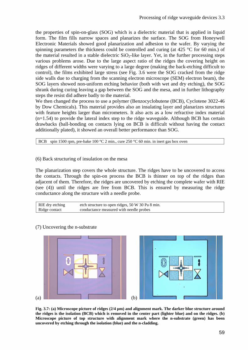
Processing of ridge waveguide devices 3.3
the properties of spin-on-glass (SOG) which is a dielectric material that is applied in liquid form. The film fills narrow spaces and planarizes the surface. The SOG from Honeywell Electronic Materials showed good planarization and adhesion to the wafer. By varying the
inning parameters the thickness could be controlled and curing (at 425 °C for 60 min.) of the material resulted in a stable dielectric SiO2-like layer. Yet, in the further processing steps various problems arose. Due to the large aspect ratio of the ridges the covering height on ridges of different widths were varying to a large degree (making the back-etching difficult to control), the films exhibited large stress (see Fig. 3.6 were the SOG cracked from the ridge side walls due to charging from the scanning electron microscope (SEM) electron beam), the SOG layers showed non-uniform etching behavior (both with wet and dry etching), the SOG shrank during curing leaving a gap between the SOG and the mesa, and in further lithography steps the resist did adhere badly to the material. We then changed the process to use a polymer (Benzocyclobutene (BCB), Cyclotene 3022-46
ow Chemicals). This material provides ting layer and planarizes structures ith feature heights larger than micrometers. It also acts as a low refractive index material
sp
by D also an insulaw(n=1.54) to provide the lateral index step to the ridge waveguide. Although BCB has certain drawbacks (ball-bonding on contacts lying on BCB is difficult without having the contact additionally plated), it showed an overall better performance than SOG.
BCB spin 1500 rpm, pre-bake 100 °C 2 min., cure 250 °C 60 min. in inert gas box oven (6) Back structuring of insulation on the mesa The planarization step covers the whole structure. The ridges have to be uncovered to access the contacts. Through the spin-on process the BCB is thinner on top of the ridges than adjacent of them. Therefore, the ridges are uncovered by etching the complete wafer with RIE (see (4)) until the ridges are free from BCB. This is ensured by measuring the ridge conductance along the structure with a needle probe.
RIE dry etching etch structure to open ridges, 50 W 30 Pa 8 min. Ridge contact conductance measured with needle probes
(7) Uncovering the n-substrate
(a) (b) Fig. 3.7: (a) Microscope picture of ridges (2/4 µm) and alignment mark. The darker blue structure around the ridges is the isolation (BCB) which is removed in the center part (lighter blue) and on the ridges. (b) Microscope picture of top structure with alignment mark where the n-substrate (green) has been uncovered by etching through the isolation (blue) and the n-cladding.
59
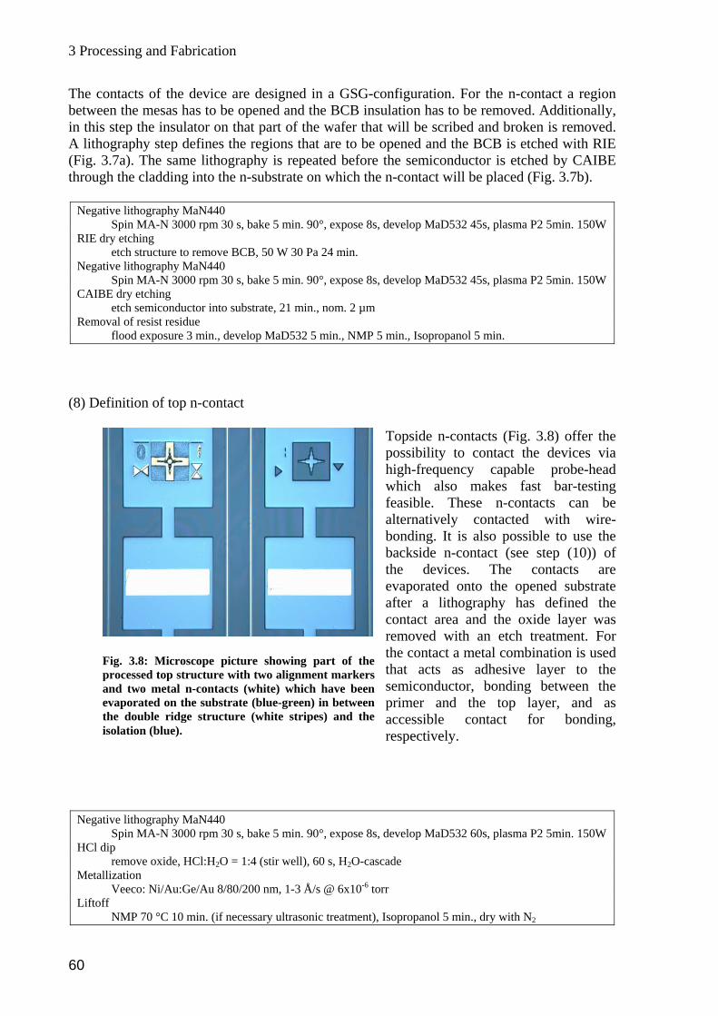
3 Processing and Fabrication
The contacts of the device are designed in a GSG-configuration. For the n-contact a region between the mesas has to be opened and the BCB insulation has to be removed. Additionally, in this step the insulator on that part of the wafer that will be scribed and broken is removed. A lithography step defines the regions that are to be opened and the BCB is etched with RIE (Fig. 3.7a). The same lithography is repeated before the semiconductor is etched by CAIBE through the cladding into the n-substrate on which the n-contact will be placed (Fig. 3.7b).
Negative lithography MaN440 Spin MA-N 3000 rpm 30 s, bake 5 min. 90°, expose 8s, develop MaD532 45s, plasma P2 5min. 150W
RIE dry etching etch structure to remove BCB, 50 W 30 Pa 24 min. Negative lithography MaN440
Spin MA-N 3000 rpm 30 s, bake 5 min. 90°, expose 8s, develop MaD532 45s, plasma P2 5min. 150W CAIBE dry etching etch semiconductor into substrate, 21 min., nom. 2 µm Removal of resist residue flood exposure 3 min., develop MaD532 5 min., NMP 5 min., Isopropanol 5 min.
(8) Definition of top n-contact
Topside n-contacts (Fpossibility to contact the devices via
ig. 3.8) offer the
high-frequency capable probe-head which also makes fast bar-testing feasible. These n-contacts can be
after a lithography has defined the rea and the oxide layer was
with an etch treatment. For tact a metal combination is used
that acts as adhesive layer to the semiconductor, bonding between the primer and the top layer, and as accessible contact for bonding, respectively.
Negative lithography MaN440
alternatively contacted with wire-bonding. It is also possible to use the backside n-contact (see step (10)) of the devices. The contacts are evaporated onto the opened substrate
contact aoved rem
the con Fig. 3.8: Microscope picture showing part of the processed top structure with two alignment markers and two metal n-contacts (white) which have been evaporated on the substrate (blue-green) in between the double ridge structure (white stripes) and the isolation (blue).
Spin MA-N 3000 rpm 30 s, bake 5 min. 90°, expose 8s, develop MaD532 60s, plasma P2 5min. 150W HCl dip
remove oxide, HCl:H2O = 1:4 (stir well), 60 s, H2O-cascade Metallization
Veeco: Ni/Au:Ge/Au 8/80/200 nm, 1-3 Å/s @ 6x10⁻⁶ torr Liftoff
NMP 70 °C 10 min. (if necessary ultrasonic treatment), Isopropanol 5 min., dry with N2
60
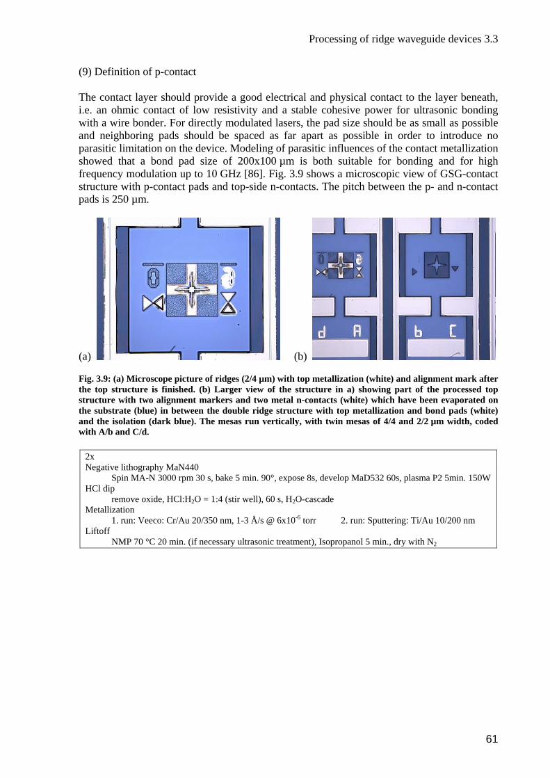
Processing of ridge waveguide devices 3.3
(9) Definition of p-contact The contact layer should provide a good electrical and physical contact to the layer beneath, i.e. an ohmic contact of low resistivity and a stable cohesive power for ultrasonic bonding with a wire bonder. For directly modulated lasers, the pad size should be as small as possible and neighboring pads should be spaced as far apart as possible in order to introduce no parasitic limitation on the device. Modeling of parasitic influences of the contact metallization showed that a bond pad size of 200x100 µm is both suitable for bonding and for high frequency modulation up to 10 GHz [86]. Fig. 3.9 shows a microscopic view of GSG-contact structure with p-contact pads and top-side n-contacts. The pitch between the p- and n-contact
is 250 µm. pads
(a) (b) Fth showing part of the processed top st ontacts (white) which have been evaporated on th a with
x
ig. 3.9: (a) Microscope picture o top
f ridges (2/4 µm) with top metallization (white) and alignment mark after e structure is finished. (b) Larger view of the structure in a)
arkers and two metal n-cructure with two alignment me substrate (blue) in between the double ridge structure with top metallization and bond pads (white)
rk blue). The mesas run vertically, with twin mesas of 4/4 and 2/2 µm width, codednd the isolation (daA/b and C/d.
2Negative lithography MaN440
Spin MA-N 3000 rpm 30 s, bake 5 min. 90°, expose 8s, develop MaD532 60s, plasma P2 5min. 150W HCl dip
remove oxide, HCl:H2O = 1:4 (stir well), 60 s, H2O-cascade Metallization
1. run: Veeco: Cr/Au 20/350 nm, 1-3 Å/s @ 6x10⁻⁶ torr 2. run: Sputtering: Ti/Au 10/200 nm Liftoff
NMP 70 °C 20 min. (if necessary ultrasonic treatment), Isopropanol 5 min., dry with N2
61
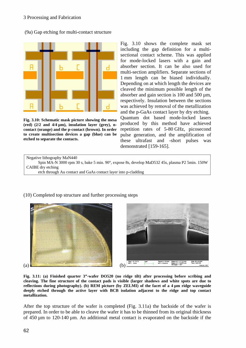
3 Processing and Fabrication
(9a) Gap etching for multi-contact structure
Fig. includsectiofor mabsormulti1 mmDepecleavabsorres
pulse generation, and the amplification of these ultrafast and -short pulses was demonstrated [159-165].
Negative lithography MaN440
3.10 shows the complete mask set ing the gap definition for a multi-nal contact scheme. This was applied ode-locked lasers with a gain and
ber section. It can be also used for -section amplifiers. Separate sections of length can be biased individually. nding on at which length the devices are ed the minimum possible length of the ber and gain section is 100 and 500 µm, ctively. Insulation between the sections chieved by removal of the metallization e p-GaAs contact layer by dry etching.
tum dot based mode-locked lasers ced by this method have achieved tion rates of 5-80 GHz, picosecond
pewas aand thQuanprodurepeti
Fig. 3.10: Schematic mask picture showing the mesa (red) (2/2 and 4/4 µm), insulation layer (grey), n-contact (orange) and the p-contact (brown). In order to cre devices a gap (blue) can be ate multisection etched to separate the contacts.
Spin MA-N 3000 rpm 30 s, bake 5 min. 90°, expose 8s, develop MaD532 45s, plasma P2 5min. 150W CAIBE dry etching etc uh thro gh Au contact and GaAs contact layer into p-cladding
(10) Completed top structure and further processing steps
(a) (b) Fig. 3.11: (a) Finished quarter 3”-wafer DO520 (no ridge tilt) after processing before scribing and cleaving. The fine structure of the contact pads is visible (larger shadows and white spots are due to reflections during photography). (b) REM picture (by ZELMI) of the facet of a 4 µm ridge waveguide deeply etched through the active layer with BCB isolation adjacent to the ridge and top contact metallization. After the top structure of the wafer is completed (Fig. 3.11a) the backside of the wafer is prepared. In order to be able to cleave the wafer it has to be thinned from its original thickness of 450 µm to 120-140 µm. An additional metal contact is evaporated on the backside if the
62
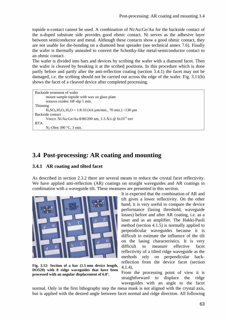
Post-processing: AR coating and mounting 3.4
topside n-contact cannot be used. A combination of Ni/Au:Ge/Au for the backside contact of the n-doped substrate side provides good ohmic contact. Ni serves as the adhesive layer between semiconductor and metal. Although these contacts show a good ohmic contact, they are not usable for die-bonding on a diamond heat spreader (see technical annex 7.6). Finally the wafer is thermally annealed to convert the Schottky-like metal-semiconductor contact to an ohmic contact. The wafer is divided into bars and devices by scribing the wafer with a diamond facet. Then the wafer is cleaved by breaking it at the scribed positions. In this procedure which is done partly before and partly after the anti-reflection coating (section 3.4.1) the facet may not be damaged, i.e. the scribing should not be carried out across the edge of the wafer. Fig. 3.11(b)
s the facet of a cleaved device after com rocessing. show pleted p
Backside treatment of wafer mount sample topside with wax on glass plate
remove oxides: HF-dip 1 min. Thinning
H2SO4:H2O2:H2O = 1:8:10 (4.6 µm/min., 70 min.) ~130 µm Backside contact
Veeco: Ni/Au:Ge/Au 8/80/200 nm, 1-3 Å/s @ 6x10⁻⁶ torr RTA N2-Ofen 390 °C, 3 min.
3 ost-processing: AR coating and mounting
.4.1 AR coating and tilted facet
s described in section 2.3.2 there are several means to reduce the crystal facet reflectivity. e have applied anti-reflection (AR) coatings on straight waveguides and AR coatings in
ombination with a waveguide tilt. These measures are presented in this section. It is expected that the combination of AR and tilt gives a lower reflectivity. On the other hand, it is very useful to compare the device performance (lasing threshold, waveguide losses) before and after AR coating, i.e. as a laser and as an amplifier. The Hakki-Paoli method (section 4.1.5) is normally applied to perpendicular waveguides because it is difficult to estimate the influence of the tilt on the lasing characteristics. It is very difficult to measure effective facet reflectivity of a tilted ridge waveguide as the methods rely on perpendicular back-reflection from the device facet (section 4.1.4). From the processing point of view it is straightforward to displace the ridge waveguides with an angle to the facet
normal. Only in the first lithography step the mesa mask is not aligned with the crystal axis, but is applied with the desired angle between facet normal and ridge direction. All following
.4 P3 AWc
Fig. 3.12: Section of a bar (1.5 mm device length, DO520) with 8 ridge waveguides that have been processed with an angular displacement of 6.8°.
63
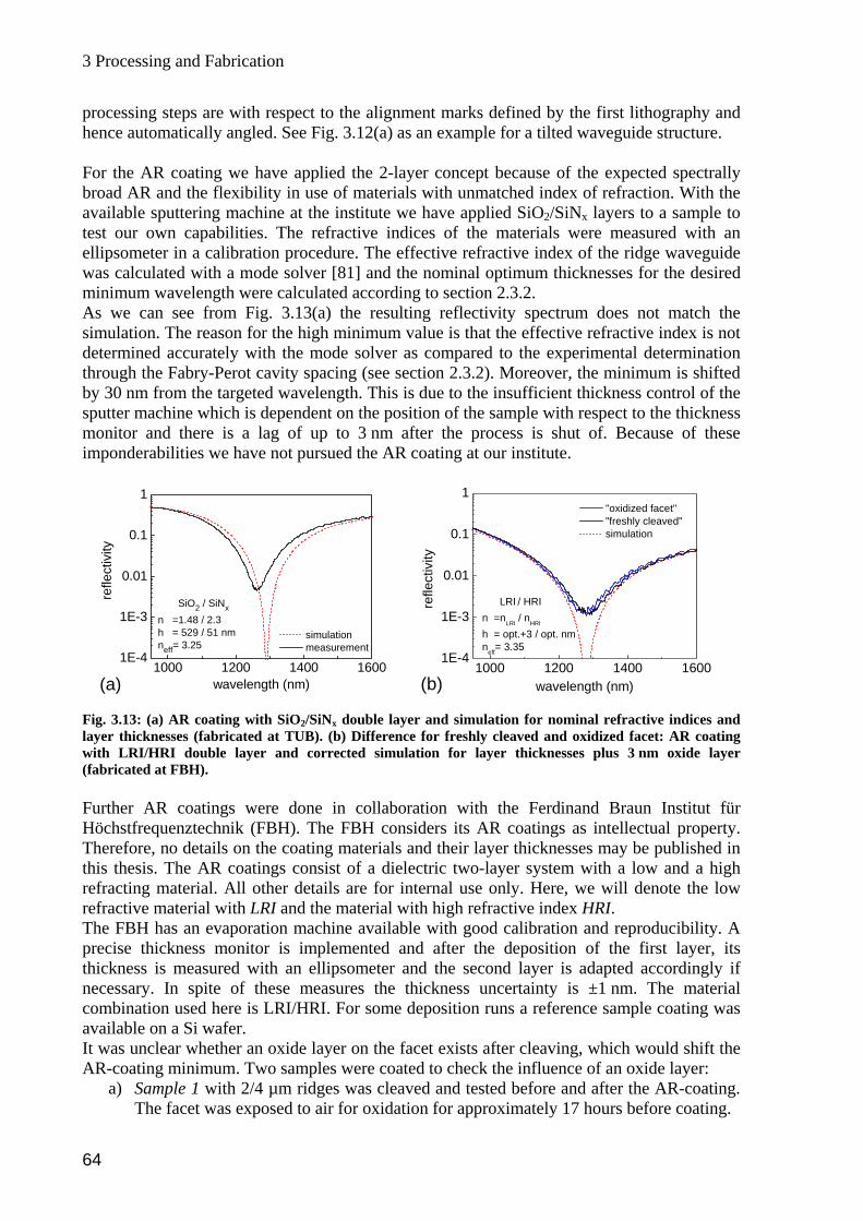
3 Processing and Fabrication
processing steps are with respect to the alignmehence automatically angled. See Fig. 3.12(a) as a For the AR coating we have applied the 2-layebroad AR and the flexibility in use of materials available sputtering machine at the institute we test our own capabilities. The refractive indicellipsometer in a calibration procedure. The effewas calculated with a mode solver [81] and the minimum wavelength were calculated accordingAs we can see from Fig. 3.13(a) the resultinsimulation. The reason for the high minimum vaetermined accurately with the mode solver a
t i
t pursued the AR c
1
nt marks defined by the first lithography and n example for a tilted waveguide structure.
r concept because of the expected spectrally with unmatched index of refraction. With the have applied SiO2/SiNx layers to a sample to es of the materials were measured with an ctive refractive index of the ridge waveguide nominal optimum thicknesses for the desired to section 2.3.2. g reflectivity spectrum does not match the lue is that the effective refractive index is not
compared to the experimental determination d sthrough the Fabry-Perot cavity spacing (see secby 30 nm from the targeted wavelength. This issputter machine which is dependent on the positmonitor and there is a lag of up to 3 nm aftimponderabilities we have no
ion 2.3.2). Moreover, the minimum is shifted due to the insufficient thickness control of the on of the sample with respect to the thickness er the process is shut of. Because of these oating at our institute.
1000 1200 1400 16001E-4
1E-3
0.01
0.1
simulation measurement
h = 529 / 51 nmneff= 3.25
refle
wavelength (nm)
SiO2 / SiNxn =1.48 / 2.3
(a)
1
ctiv
ity
1000 1200 1400 16001E-4
1E-3
0.01
"oxidized facet" "freshly cleaved" simulation0.1
tivity
refle
c
wavelength (nm)
LRI / HRIn =nLRI / nHRI
= opt.+3 / opt. nm= 3.35
(b)
Fig. 3.13: (a) AR coating with SiO2/SiNx double layer and simulation for nominal refractive indices and layer thicknesses (fabricated at TUB). (b) Difference for freshly cleaved and oxidized facet: AR coating with LRI/HRI double layer and corrected simulation for layer thicknesses plus 3 nm oxide layer (fabricated at FBH). Further AR coatings were done in collaboration with the Ferdinand Braun Institut für Höchstfrequenztechnik (FBH). The FBH considers its AR coatings as intellectual property. Therefore, no details on the coating materials and their layer thicknesses may be published in this thesis. The AR coatings consist of a dielectric two-layer system with a low and a high
aterial. All other details are for l use only. Here, we will denote the low fractive material with LRI and the material with high refractive index HRI.
LRI/HRI. For some deposition runs a reference sample coating was
h neff
refracting m internareThe FBH has an evaporation machine available with good calibration and reproducibility. A precise thickness monitor is implemented and after the deposition of the first layer, its thickness is measured with an ellipsometer and the second layer is adapted accordingly if necessary. In spite of these measures the thickness uncertainty is ±1 nm. The material ombination used here isc
available on a Si wafer. It was unclear whether an oxide layer on the facet exists after cleaving, which would shift the AR-coating minimum. Two samples were coated to check the influence of an oxide layer:
a) Sample 1 with 2/4 µm ridges was cleaved and tested before and after the AR-coating. The facet was exposed to air for oxidation for approximately 17 hours before coating.
64
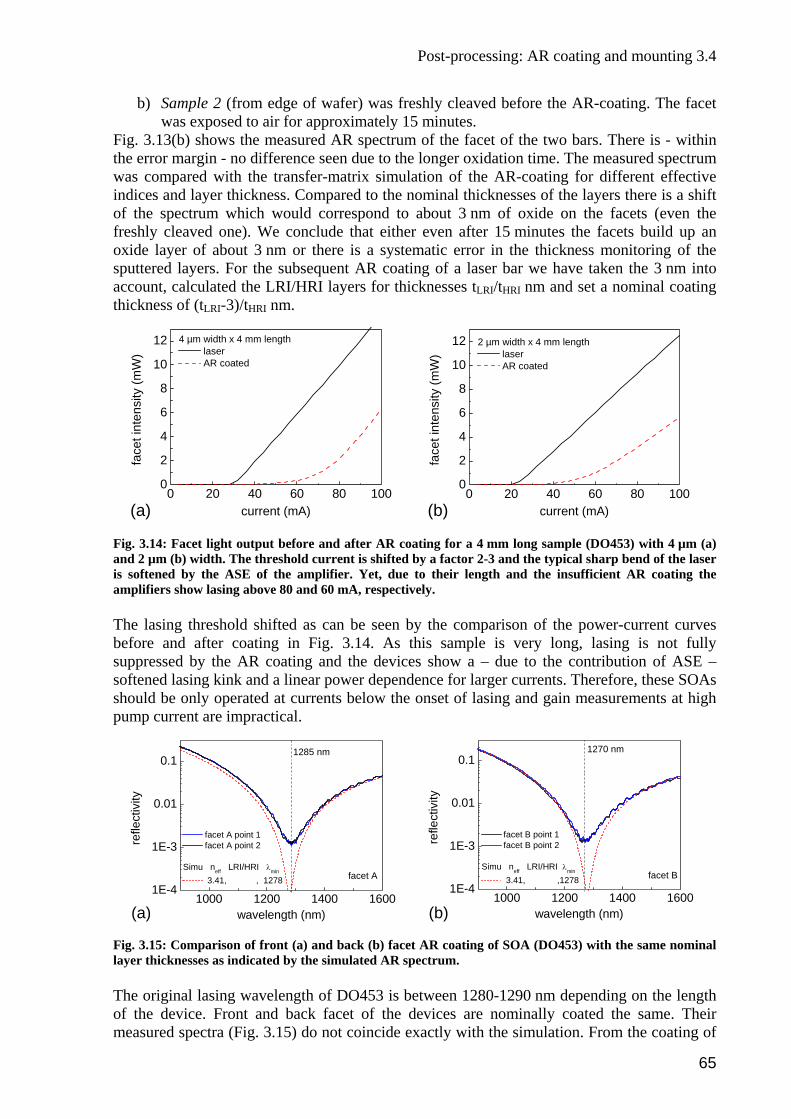
Post-processing: AR coating and mounting 3.4
b) Sample 2 (from edge of wafer) was freshly cleaved before the AR-coating. The facet was exposed to air for approximately 15 minutes.
Fig. 3.13(b) shows the measured AR spectrum of the facet of the two bars. There is - within the error margin - no difference seen due to the longer oxidation time. The measured spectrum
thickness monitoring of the uttered layers. For the subsequent AR coating of a laser bar we have taken the 3 nm into
account, calculated the LRI/HRI layers for thicknesses tLRI/tHRI nm and set a nominal coating thickne
was compared with the transfer-matrix simulation of the AR-coating for different effective indices and layer thickness. Compared to the nominal thicknesses of the layers there is a shift of the spectrum which would correspond to about 3 nm of oxide on the facets (even the freshly cleaved one). We conclude that either even after 15 minutes the facets build up an oxide layer of about 3 nm or there is a systematic error in thesp
ss of (t -3)/t nm. LRI HRI
0 20 40 60 80 1000
2
4
6
8
10
12 4 µm width x 4 mm length laser AR coatedW
)
face
(mt i
nten
sity
current (mA)(a)0 20 40 60 80 100
0
2
4
6
8
10
12 2 µm width x 4 mm length laser AR coated
face
t int
ensi
tW
)
t (mA)
4 AR coating for a 4 mm long sample (DO453) with 4 µm (a) shifted by a factor 2-3 and the typical sharp bend of the laser
rrent curves efore and after coating in Fig. 3.14. As th
suppressed by the AR coating and the devicessoftened lasing kink and a linear power dependeshould be only operated at currents below the opump current are impractical.
y (m
curren(b)
Fig. 3.1 : Facet light output before and afternd 2 µm (b) width. The threshold current is a
is softened by the ASE of the amplifier. Yet, due to their length and the insufficient AR coating the amplifiers show lasing above 80 and 60 mA, respectively. The lasing threshold shifted as can be seen by the comparison of the power-cub is sample is very long, lasing is not fully
show a – due to the contribution of ASE – nce for larger currents. Therefore, these SOAs nset of lasing and gain measurements at high
1000 1200 1400 16001E-4
1E-3
0.01
0.1
facet A point 1 facet A point 2
Simu neff LRI/HRI λmin
3.41, , 1278
refle
ctiv
ity
wavelength (nm)
1285 nm
facet A
(a)1000 1200 1400 1600
1E-4
1E-3
0.01
0.1
facet B point 1 facet B point 2
Simu neff LRI/HRI λmin
3.41, ,1278
refle
ctiv
ity
1270 nm
facet B
wavelength (nm)(b)
R coating of SOA (DO453) with the same nominal layer thicknesses as indicated by the simulated AR spectrum. The original lasing wavelength of DO453 is between 1280-1290 nm depending on the length of the device. Front and back facet of the devices are nominally coated the same. Their measured spectra (Fig. 3.15) do not coincide exactly with the simulation. From the coating o
Fig. 3.15: Comparison of front (a) and back (b) facet A
f
65
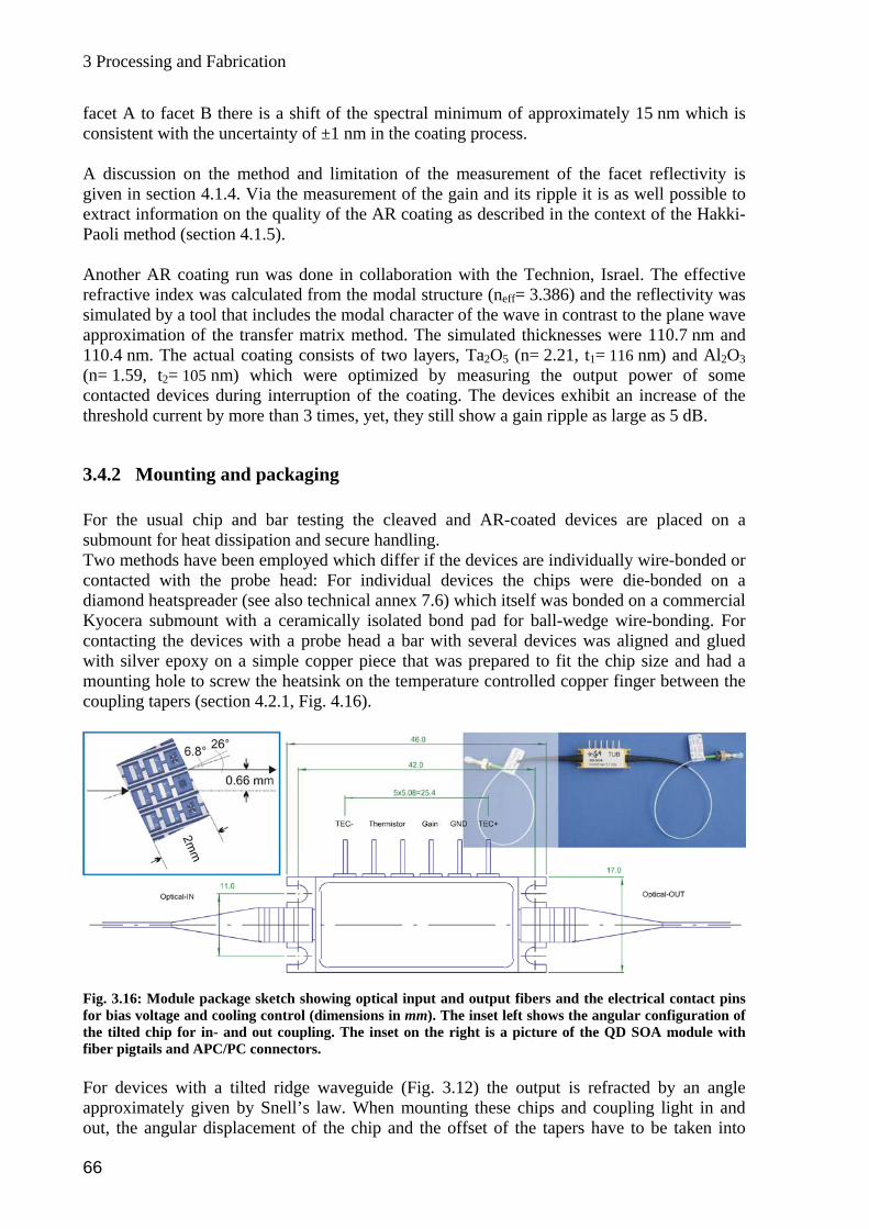
3 Processing and Fabrication
facet A to facet B there is a shift of the spectral minimum of approximately 15 nm which is
3.4.2 Mounting and packaging For the usual chip and bar testing the cleaved and AR-coated devices are placed on a submount for heat dissipation and secure handling. Two methods have been employed which differ if the devices are individually wire-bonded or contacted with the probe head: For individual devices the chips were die-bonded on a diamond heatspreader (see also technical annex 7.6) which itself was bonded on a commercial Kyocera submount with a ceramically isolated bond pad for ball-wedge wire-bonding. For contacting the devices with a probe head a bar with several devices was aligned and glued with silver epoxy on a simple copper piece that was prepared to fit the chip size and had a
consistent with the uncertainty of ±1 nm in the coating process. A discussion on the method and limitation of the measurement of the facet reflectivity is given in section 4.1.4. Via the measurement of the gain and its ripple it is as well possible to extract information on the quality of the AR coating as described in the context of the Hakki-Paoli method (section 4.1.5). Another AR coating run was done in collaboration with the Technion, Israel. The effective refractive index was calculated from the modal structure (neff= 3.386) and the reflectivity was simulated by a tool that includes the modal character of the wave in contrast to the plane wave approximation of the transfer matrix method. The simulated thicknesses were 110.7 nm and 110.4 nm. The actual coating consists of two layers, Ta2O5 (n= 2.21, t1= 116 nm) and Al2O3 (n= 1.59, t2= 105 nm) which were optimized by measuring the output power of some contacted devices during interruption of the coating. The devices exhibit an increase of the threshold current by more than 3 times, yet, they still show a gain ripple as large as 5 dB.
mounting hole to screw the heatsink on the temperature controlled copper finger between the coupling tapers (section 4.2.1, Fig. 4.16).
Fig. 3.16: Module package sketch showing optical input and output fibers and the electrical contact pins
ith
Forappout, the ang
for bias voltage and cooling control (dimensions in mm). The inset left shows the angular configuration of the tilted chip for in- and out coupling. The inset on the right is a picture of the QD SOA module wfiber pigtails and APC/PC connectors.
devices with a tilted ridge waveguide (Fig. 3.12) the output is refracted by an angle roximately given by Snell’s law. When mounting these chips and coupling light in and
ular displacement of the chip and the offset of the tapers have to be taken into
66
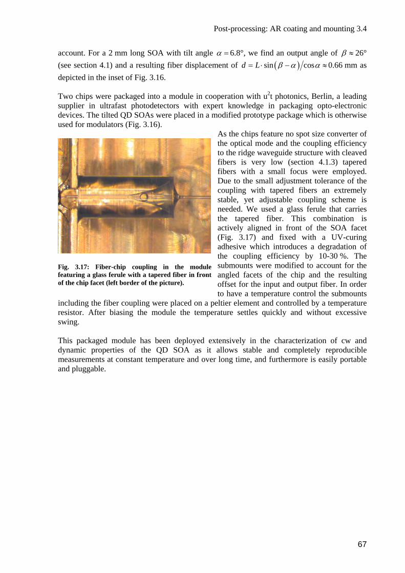
Post-processing: AR coating and mounting 3.4
account. For a 2 mm long SOA with tilt angle =α 6.8°, we find an output angle of ≈β 26° (see section 4.1) and a resulting fiber displacement of ( )sin cos= ⋅ − ≈d L β α α 0.66 mm as depicted in the inset of Fig. 3.16. Two chips were packaged into a module in cooperation with u2t photonics, Berlin, a leading supplier in ultrafast photodetectors with expert knowledge in packaging opto-electronic devices. The tilted QD SOAs were placed in a modified prototype package which is otherwise used for modulators (Fig. 3.16).
As the chips feature no spot size converter of the optical mode and the coupling efficiency to the ridge waveguide structure with cleaved fibers is very low (section 4.1.3) tapered fibers with a small focus were employed. Due to the small adjustment tolerance of the coupling with tapered fibers an extremely stable, yet adjustable coupling scheme is needed. We used a glass ferule that carries the tapered fiber. This combination is actively aligned in front of the SOA facet (Fig. 3.17) and fixed with a UV-curing adhesive which introduces a degradation of
set for the input and output fiber. In order to have a temperature control the submounts
D SOA as it allows stable and completely reproducible measurements at constant temperature and over long time, and furthermore is easily portable and pluggable.
the coupling efficiency by 10-30 %. The submounts were modified to account for the angled facets of the chip and the resulting off
Fig. 3.17: Fiber-chip coupling in the module featuring a glass ferule with a tapered fiber in front of the chip facet (left border of the picture).
including the fiber coupling were placed on a peltier element and controlled by a temperature resistor. After biasing the module the temperature settles quickly and without excessive swing. This packaged module has been deployed extensively in the characterization of cw and dynamic properties of the Q
67
4 General Device Characterization and Measurement Techniques
4 General Device Characterization and Measurement Techniques
The device performance with regard to far field, coupling losses, facet reflectivity and gain-reflectivity product should be assessed before the measurement of the cw and dynamic gain characteristics. These preliminary general device characterizations are presented in the first part of this chapter together with the corresponding measurement techniques.
The implementation of measurement techniques for the characterization of SOAs was one of the goals of this thesis. In the second part the setups and measurement techniques for gain, noise, pump probe, bit error ratio and XGM measurements are introduced and described. The corresponding results will be discussed in full detail in chapter 5. 4.1 General device characterization
Table 4: List of sample structures that are presented in this work.
Wafer QD layers Peak λ AR Tilt Etching Widths Lengths
4.1.1 List of samples Table 4 lists all samples with their key properties that were used in this work. The wafer Ioffe4915 was grown at the Ioffe Physico-Technical Institute, St. Petersburg. The wafers starting with DO were grown by NL Nanosemiconductor, Dortmund. The samples of the Ioffe4915 wafer did not show positive fiber-to-fiber gain and are only considered in the far field measurements. DO75 is a laser structure with no AR coating. The sample was used for M2- and far field measurements. Its epitaxial structure is comparable to DO520. Samples DO453 and DO520 are considered the workhorses of this thesis, all cw and dynamic gain
vestigation were done with these sample structures. in
Ioffe4915 5 1270 nm No 7° Shallow 6 µm 2 mm Ioffe4915 5 1270 nm Yes No Shallow 4 µm 2 mm Ioffe4915 5 1270 nm Yes No Deep 4 µm 2 mm
DO75 10 1270 nm No No Deep 1/2/4 µm 1 mm DO453 15 1280 nm Yes No Deep 2/4 µm 2/4 mm DO520 10 1290 nm Yes 6.8° Deep 2/4 µm 2 mm
es the modal structure of the waveguide and indicates with
and its measurement gives a figure of merit that characterizes the quality of the beam. 2) The direct
4.1.2 Far field measurement For a SOA the far field characterizwhat efficiency light can be coupled to and from the device. Therfore, the far field is the starting point in the assessment of the amplifier performance.
The far field of an optical source is characterized by two methods in this section: 1) The deviation from an ideal Gaussian mode is described by the so-called 2M -factor
68
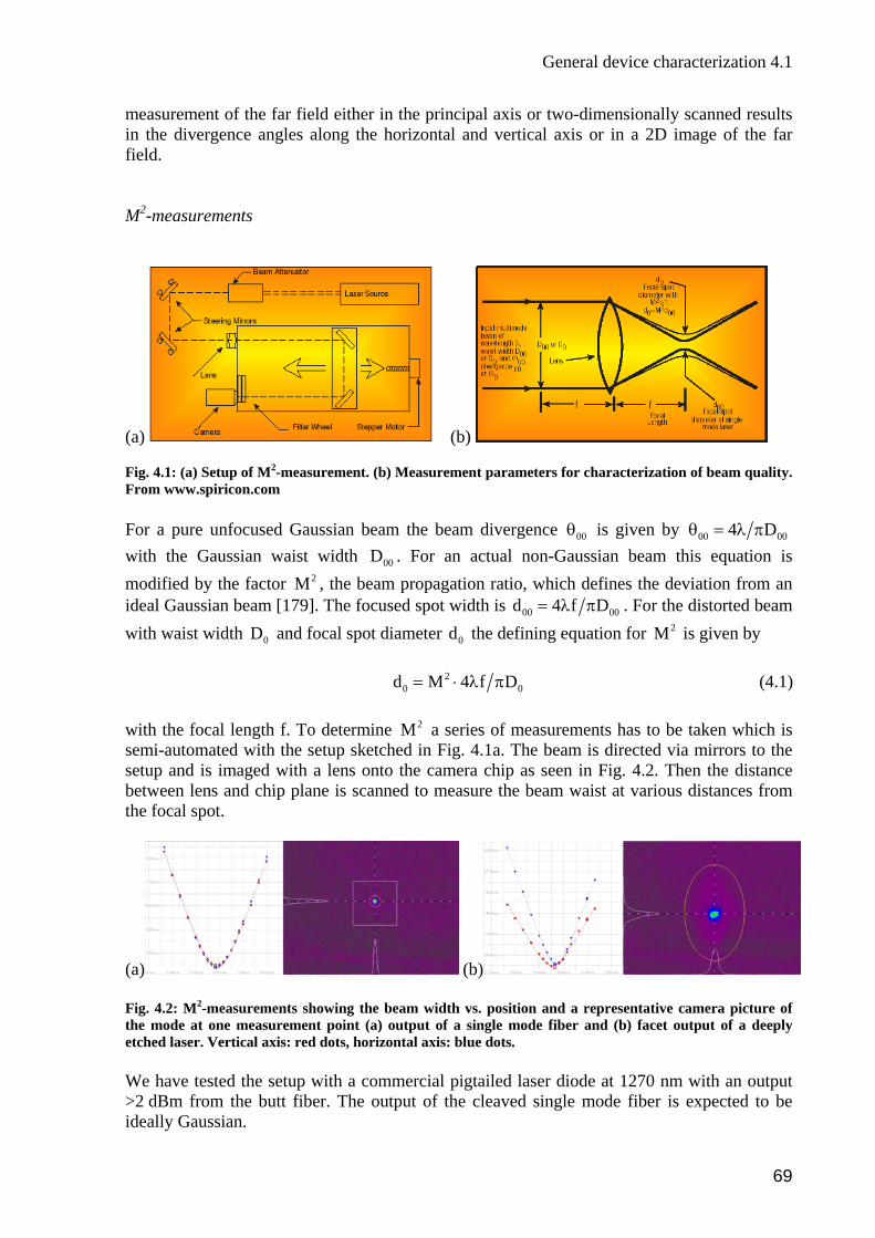
General device characterization 4.1
measurement of the far field either in the principal axis nned results in the divergence angles along th
ld.
or two-dimensionally scae horizontal and vertical axis or in a 2D image of the far
(a)
fie M2-measurements
(b)
nt parameters for characterization of beam quality.
divergence 00
Fig. 4.1: (a) Setup of M2-measurement. (b) MeasuremeFrom www.spiricon.com
or a pure unfocused Gaussian beam the beaF m θ is given by 00 004 Dθ = λ π actual non-Gaussian beam this equation is on ratio, which defines the deviation from an dth is
with the Gaussian waist width 00D . For an modified by the factor 2M , the beam propagatiideal Gaussian beam [1 The f d spot wi79]. ocuse 00 00d 4 f D= λ π . For the distorted beam with waist width 0D and focal spot diameter 0d the defining equation for 2M is given by
20 0d M 4 f D= ⋅ λ π (4.1)
onto the camera chip as seen in Fig. 4.2. Then the distance etween lens and chip plane is scanned to measure the beam waist at various distances from e focal spot.
(a)
with the focal length f. To determine 2M a series of measurements has to be taken which is semi-automated with the setup sketched in Fig. 4.1a. The beam is directed via mirrors to the setup and is imaged with a lensbth
(b) Fig. 4.2: M2-measurements showing the beam width vs. position and a representative camera picture of the mode at one measurement point (a) output of a single mode fiber and (b) facet output of a deeply etched laser. Vertical axis: red dots, horizontal axis: blue dots. We have tested the setup with a commercial pigtailed laser diode at 1270 nm with an output >2 dBm from the butt fiber. The output of the cleaved single mode fiber is expected to be ideally Gaussian.
69
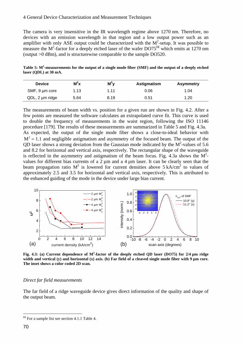
4 General Device Characterization and Measurement Techniques
The camera is very insensitive in the IR wavelength regime above 12devices with an emission wavelength in that region and a low outp
lifier with only ASE output could be character2-factor for a deeply etched laser of the wafer DO75
70 nm. Therefore, no ut power such as an
amp ized with the M2-setup. It was possible to easure the M 11 which emits at 1270 nm utput >0 dBm), and is structurewise comparable to the sample DO520.
Asymmetry
m(o Table 5: M2-measurements for the output of a single mode fiber (SMF) and the output of a deeply etched laser (QDL) at 30 mA.
Device M2x M2y Astigmatism SMF, 9 µm core 1.13 1.11 0.06 1.04
QDL, 2 µm ridge 5.64 8.19 0.51 1.20
he measurements of beam width vs. position for a given run are shown in Fig. 4.2. After aT w points are measured the software calculates an extrapolated curve fit. This curve is used
ist region, following the ISO 11146 summarized in Table 5 and Fig. 4.3a.
p of the single mode fiber shows a close-to-ideal behavior with atism and asymmetry of the focused beam. The output of the
D laser shows a strong deviation from the Gaussian mode indicated by the M2-values of 5.6
4
feto double the frequency of measurements in the waprocedure [179]. The results of these measurements are As ex ected, the output
2M = 1.1 and negligible astigmQand 8.2 for horizontal and vertical axis, respectively. The rectangular shape of the waveguide is reflected in the asymmetry and astigmatism of the beam focus. Fig. 4.3a shows the M2-values for different bias currents of a 2 µm and a 4 µm laser. It can be clearly seen that the beam propagation ratio M2 is lowered for current densities above 5 kA/cm2 to values of approximately 2.5 and 3.5 for horizontal and vertical axis, respectively. This is attributed to the enhanced guiding of the mode in the device under large bias current.
10
0 2 4 6 8 10 12 1
2
4
6
8
2 µm Mx2
2 µm M2y
4 µm M2x
4 µm M2y
M²
curre nsity (6
0
0
0
1.0
nt de kA/cm2)(a)-10
.0-8 -6 -4 -2 0 2 4 8 10
.2
.4
0.6 -4 --4
2
4
0.8
2 0 2 4
-2
0
(b)
θ1/e2 of SMF 10.8° (y) 11.2° (x)
inte
nsity
(nor
m.)
xis (
ig. 4.3: (a) Current dependence of M2-factor of the deeply etched QD laser (DO75) for 2/4 µm ridge idth and vertical (y) and horizontal (x) axis. (b) Far field of a cleaved single mode fiber with 9 µm core. he inset shows a color coded 2D scan.
scan a degrees)
FwT Direct far field measurements The far field of a ridge waveguide device gives direct information of the quality and shape of the output beam.
11 For a sample list see section 4.1.1 Table 4.
70
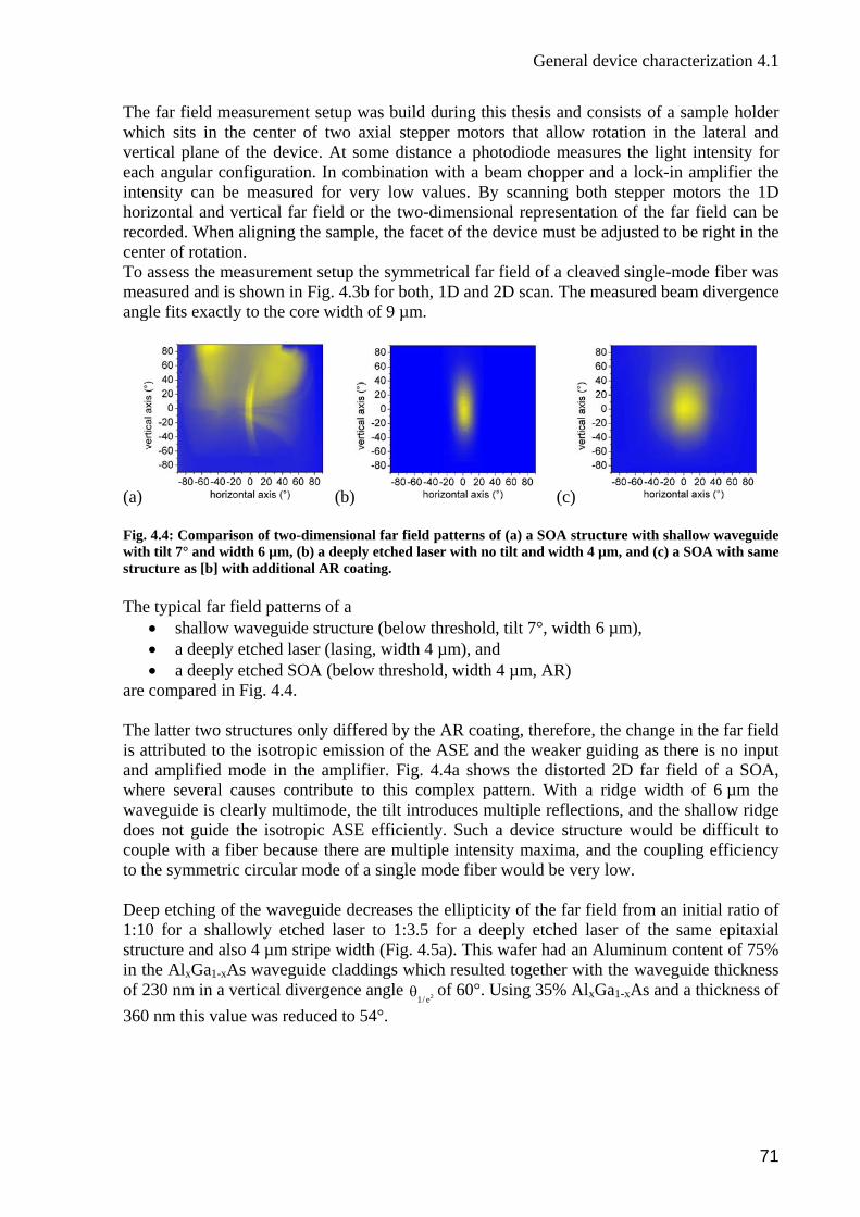
General device characterization 4.1
The far field measurement setup was build during this thesis and consists of a sample holder which sits in the center of two axial stepper motors that allow rotation in the lateral and vertical plane of the device. At some distance a photodiode measures the light intensity for ach angular configuration. In combination with a beam chopper and a lock-in amplifier the tensity can be measured for very low values. By scanning both stepper motors the 1D
ical far field or the two-dimensional representation of the far field can be corded. When aligning the sample, the facet of the device must be adjusted to be right in the
enter of rotation. To assess the measurement setup the symmetrical far field of a cleaved single-mode fiber was measured and is shown in Fig. 4.3b for both, 1D and 2D scan. The measured beam divergence angle fits exactly to the core width of 9 µm.
einhorizontal and vertrec
(a) (b) (c) Fig. 4.4: Comparison of two-dimension r field patterns of (a) a SOA structure with shallow waveguide with tilt 7° and width 6 µm, (b) a deeply hed laser with no tilt and width 4 µm, and (c) a SOA with same structure as [b] with addition AR coating. The typical far field patterns of a
• shallow w guide structure (below th shold, tilt 7°, width 6 µm),
al fa etc
al
ave re • a deeply etched laser (lasing, width 4 µm), and • a deeply etched SOA (below threshold, width 4 µ
re compared in Fig. 4.4.
learly multimode, the tilt introduces multiple reflections, and the shallow ridge opic ASE efficiently. Such a device structure would be difficult to
couple with a fiber because there are multiple intensity maxima, and the coupling efficiency to the symmetric circular mode of a single mode fiber would be very low. Deep etching of the waveguide decreases the ellipticity of the far field from an initial ratio of 1:10 for a shallowly etched laser to 1:3.5 for a deeply etched laser of the same epitaxial
cture and also 4 µm stripe width (Fig. 4.5a). This wafer had an Aluminum content of 75% the AlxGa1-xAs waveguide claddings which resulted together with the waveguide thickness
m, AR) a The latter two structures only differed by the AR coating, therefore, the change in the far field is attributed to the isotropic emission of the ASE and the weaker guiding as there is no input and amplified mode in the amplifier. Fig. 4.4a shows the distorted 2D far field of a SOA, where several causes contribute to this complex pattern. With a ridge width of 6 µm the
aveguide is cwdoes not guide the isotr
struinof 230 nm in a vertical divergence angle 21/ e
θ of 60°. Using 35% AlxGa1-xAs and a thickness of 360 nm this value was reduced to 54°.
71

4 General Device Characterization and Measurement Techniques
-80 -60 -40 -20 0 20 40 60 800.0
0.2
0.4
0.6
0.8
1.0
θ1/e2
ity (
scan )
norm
.)in
tens
axis (°
vertical hor., shallow hor., deeply
0.6
0.8
1.0
(a)-60 -40 -20 0 20 40
0.0
0.2
60 80 100
4 µm 2 µm
norm
.)
I= 1250 A/cm2
0.4
y (
rizontal axis (°)(b)
i ison of x field for shallo hed offe4915 4 µm x
inte
nsit
ho
Fd
g. 4.5: (a) Compar y far w and deeply etc laser (I 2 mm). Theivergence angle 21 e
θ is 60°, 17.5°, 6° for the vertical, horizontal deeply and horizontal shallow profile,
respectively. (b) Horizontal far field scan of ASE output of 2 and 4 µm ridge waveguide SOA (DO520) with 6.8° tilt, deeply etched. For the latter sample the dependence of the far field on ridge width was studied. By decreasing the ridge width to 1 µm, we attained a close to symmetric far field which should improve the coupling due to a matched mode profile between device and fiber taper (Fig. 4.6). On the other hand, this narrow ridge is associated with a large divergence which demands a large numerical aperture of 0.6 to collect the output beam. Such coupling optics are expensive (aspheric lenses), difficult to fabricate (fiber tapers), and show a low alignment tolerance. It would be more useful to use a ridge width of 2-4 µm while reducing the vertical divergence of the device. This cannot be simply done by enlarging the waveguide thickness, because it would support higher order modes as opposed to the single mode structure used here. Concepts like large optical cavity (LOC) or longitudinal photonic band crystal (PBC) structures for a larger vertical mode necessitate a complete redesign of the epitaxial structure, yield in general a lower overlap with the active region, but could not be applied within the framework of this thesis. The coupling loss due to the asymmetry of the optical mode can be estimated from the ellipticity ratio. The minimum (ideal) coupling loss ellipα of an asymmetric far field with ellipticity x y yw wε = = θ θx to a symmetrical optical fiber is [180]
2
ellip11
ε −⎛ ⎞α = ⎜ ⎟ε +⎝ ⎠ (4.2)
with w and θ the horizontal and vertical mode width and divergence angle, respectively.
pling losses other effects are predominant, such as a non-atching numerical aperture, non-ideal Gaussian or multi-mode emission or displacement of
distance. The coupling of the SOAs to tapered fibers will be .1.3.
x,y x,yThe deep mesa mode (DO520) with 4 µm ridge width has an ellipticity of 3 (Fig. 4.6a). For the calculated first order mode of this structure this corresponds to a minimum coupling loss f 25% or 1.25 dB. Yet, for real couo
mthe coupling optics in angle orescribed in detail in section 4d
72
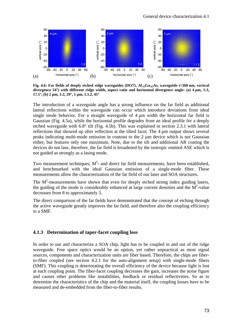
General device characterization 4.1
(a) (b) (c) Fig. 4.6: Far fields of deeply etched ridge waveguides (DO75, Al.35Ga.65As, waveguide t=360 nm, vertical
ivergence 54°) with different ridge width, aspect ratio and horizontal divergence angle: (a) 4 µm, 1:3, 17.5°, (b) 2 µm, 1:2, 29°, 1 µm, 1.1.2, 45° The introduction of a waveguide angle has a strong influence on the far field as additional lateral reflections within the waveguide can occur which introduce deviations from ideal single mode behavior. For a straight waveguide of 4 µm width the horizontal far field is Gaussian (Fig. 4.5a), while the horizontal profile degrades from an ideal profile for a deeply etched waveguide with 6.8° tilt (Fig. 4.5b). This was explained in section 2.3.1 with lateral
eflection at the tilted face 4 µm output shows several ks indicating multi-mode em ast to the 2 µm hich is not Gaussian
- and direct far field measurements, have been established, and emea r of our laser and SOA structures.
strong index guiding lasers, considerably enhanced at large current densities and the M2-value
oupling decreases the gain, increases the noise figure eedback or residual reflectivities. So as to
determine the characteristics of the chip and the material itself, the coupling losses have to be measured and de-embedded from the fiber-to-fiber results.
d
reflections that showed up after r t. Theea ission in contr device wp
either, but features only one maximum. Note, due to the tilt and additional AR coating the devices do not lase, therefore, the far field is broadened by the isotropic emitted ASE which is not guided as strongly as a lasing mode. Two measurement techniques, M2
b nchmarked with the ideal Gaussian emission of a single-mode fiber. These su ements allow the characterization of the far field
The Mthe guiding of the mode is
2-measurements have shown that even for deeply etched
decreases from 8 to approximately 3.
The direct comparison of the far fields have demonstrated that the concept of etching through the active waveguide greatly improves the far field, and therefore also the coupling efficiency to a SMF.
4.1.3 Determination of taper-facet coupling loss In order to use and characterize a SOA chip, light has to be coupled in and out of the ridge waveguide. Free space optics would be an option, yet rather unpractical as most signal sources, components and characterization units are fiber based. Therefore, the chips are fiber-to-fiber coupled (see section 4.2.1 for the auto-alignment setup) with single-mode fibers (SMF). This coupling is deteriorating the overall efficiency of the device because light is lost at each coupling point. The fiber-facet cand causes other problems like instabilities, f
73
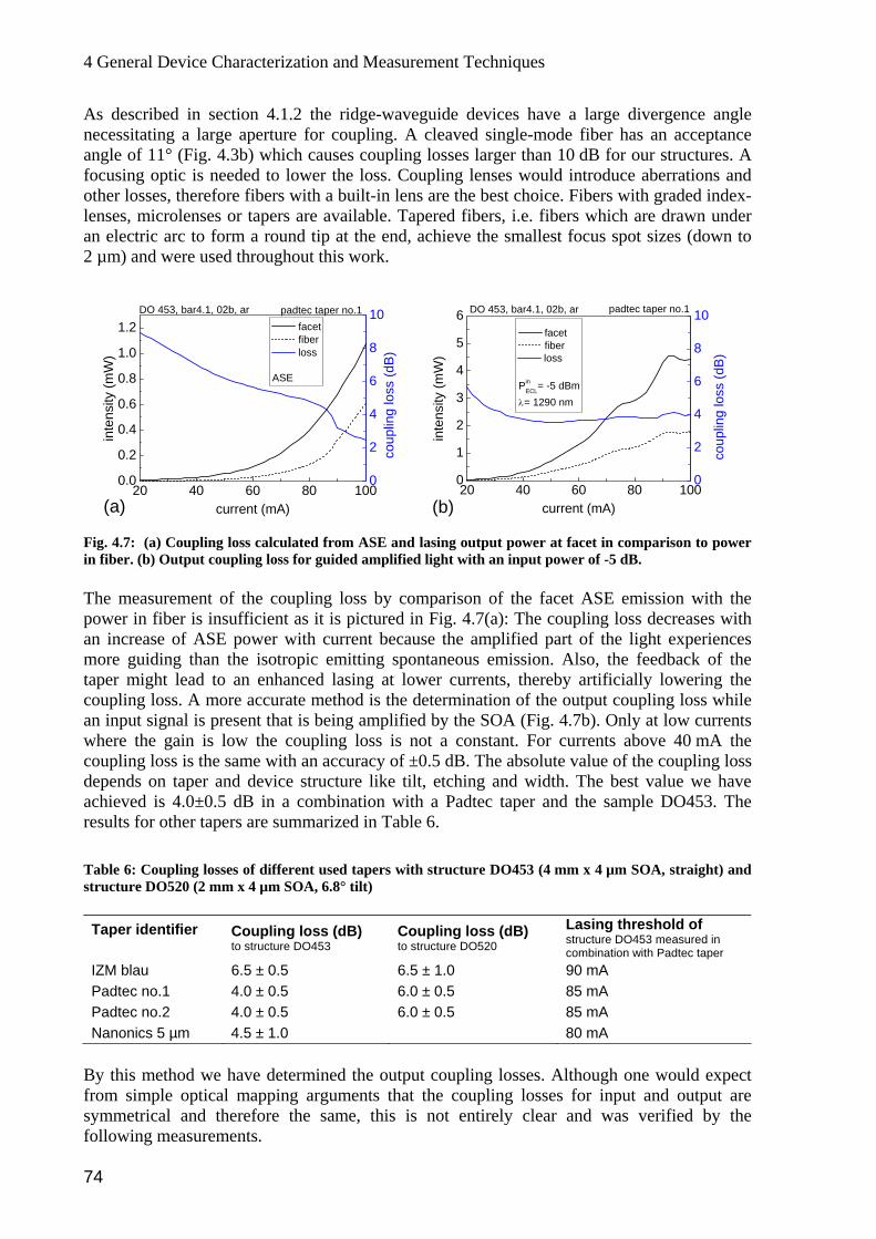
4 General Device Characterization and Measurement Techniques
As described in section 4.1.2 the ridge-waveguide devices have a large divergence angle necessitating a large aperture for coupling. A cleaved single-mode fiber has an acceptance angle of 11° (Fig. 4.3b) which causes coupling losses larger than 10 dB for our structures. A focusing optic is needed to lower the loss. Coupling lenses would introduce aberrations and other losses, therefore fibers with a built-in lens are the best choice. Fibers with graded index-lenses, microlenses or tapers are available. Tapered fibers, i.e. fibers which are drawn under an electric arc to form a round tip at the end, achieve the smallest focus spot sizes (down to 2 µm) and were used throughout this work.
20 40 60 80 1000.0
0.2
0.4
0.6
0.8
1.0
1.2
0
2
8
10
4
6
inte
nsity
(mW
)
current (mA)
facet fiber
DO 453, bar4.1, 02b, ar padtec taper no.1
ASE
(a)
loss
s (d
B)
4 c
oupl
ing
los
5
6
20 40 60 80 1000
1
2
3
DO 453, bar4.1, 02b, ar
int
0
2
8
10
4
6
ensi
ty (m
W)
facet fiber
padtec taper no.1
PinECL= -5 dBm
λ= 1290 nm
loss
ng lo
ss (d
B)
current (mA)
coup
li
The best value we have chieved is 4.0±0.5 dB in a combination with a Padtec taper and the sample DO453. The
results for other tapers are summarized in Table 6.
able 6: Coupling losses of different used tapers with structure DO453 (4 mm x 4 µm SOA, straight) and (2
(b)
Fig. 4.7: (a) Coupling loss calculated from ASE and lasing output power at facet in comparison to power in fiber. (b) Output coupling loss for guided amplified light with an input power of -5 dB. The measurement of the coupling loss by comparison of the facet ASE emission with the power in fiber is insufficient as it is pictured in Fig. 4.7(a): The coupling loss decreases with an increase of ASE power with current because the amplified part of the light experiences more guiding than the isotropic emitting spontaneous emission. Also, the feedback of the taper might lead to an enhanced lasing at lower currents, thereby artificially lowering the coupling loss. A more accurate method is the determination of the output coupling loss while an input signal is present that is being amplified by the SOA (Fig. 4.7b). Only at low currents where the gain is low the coupling loss is not a constant. For currents above 40 mA the coupling loss is the same with an accuracy of ±0.5 dB. The absolute value of the coupling loss depends on taper and device structure like tilt, etching and width. a
Tstructure DO520 mm x 4 µm SOA, 6.8° tilt) Taper identifier
Coupling loss (dB) to structure DO453
Coupling loss (dB) to structure DO520
Lasing threshold of structure DO453 measured in combination with Padtec taper
IZM blau 6.5 ± 0.5 6.5 ± 1.0 90 mA Padtec no.1 4.0 ± 0.5 6.0 ± 0.5 85 mA Padtec no.2 4.0 ± 0.5 6.0 ± 0.5 85 mA Nanonics 5 µm 4.5 ± 1.0 80 mA
By this method we have determined the output coupling losses. Although one would expect from simple optical mapping arguments that the coupling losses for input and output are symmetrical and therefore the same, this is not entirely clear and was verified by the following measurements.
74
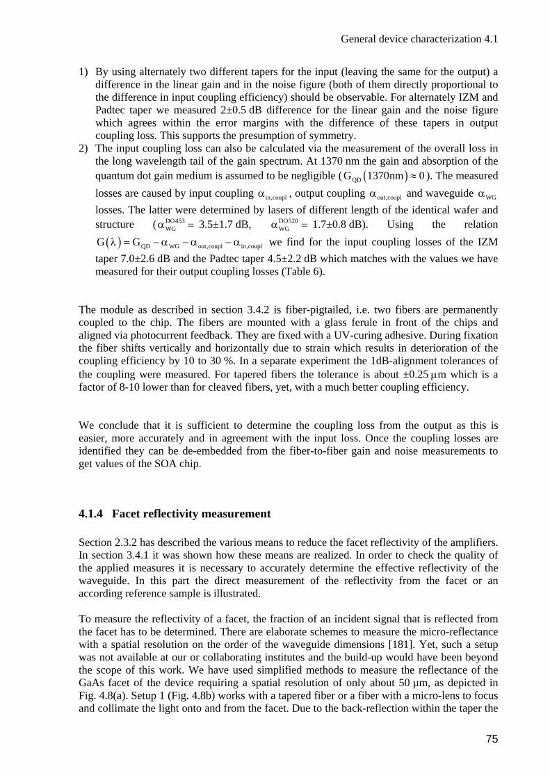
General device characterization 4.1
1) By using alternately two different tapers for the input (leaving the same for the output) a difference in the linear gain and in the noise figure (both of them directly proportional to the difference in input coupling efficiency) should be observable. For alternately IZM and Padtec taper we measured 2±0.5 dB difference for the linear gain and the noise figure which agrees within the error margins with the difference of these tapers in output coupling loss. This supports the presumption of symmetry.
2) The input coupling loss can also be calculated via the measurement of the overall loss in the long wavelength tail of the gain spectrum. At 1370 nm the gain and absorption of the quantum dot gain medium is assumed to be negligible ( ( )QDG 1370nm 0≈ ). The measured losses are caused by input coupling , output coupling and waveguide in,couplα out,couplα WGα losses. The latter were determined by lasers of different length of the identical wafer and structure ( DO453
WGα = 3.5±1.7 d DO520B, WGα = 1.7±0.8 dB). Using the relation
eparate experiment the 1dB-alignment tolerances of e coupling were measured. For tapered fibers the tolerance is about ±0.25 µm which is a
.1.4 Facet reflectivity measurement
ity of the amplifiers. zed. In order to check the quality of
e applied measures it is necessary to accurately determine the effective reflectivity of the
only about 50 µm, as depicted in ig. 4.8(a). Setup 1 (Fig. 4.8b) works with a tapered fiber or a fiber with a micro-lens to focus
and collimate the light onto and from the facet. Due to the back-reflection within the taper the
( ) QD WG out,coupl in,couplG Gλ = − α − α − α we find for the input coupling losses of the IZM taper 7.0±2.6 dB and the Padtec taper 4.5±2.2 dB which matches with the values we have measured for their output coupling losses (Table 6).
The module as described in section 3.4.2 is fiber-pigtailed, i.e. two fibers are permanently coupled to the chip. The fibers are mounted with a glass ferule in front of the chips and aligned via photocurrent feedback. They are fixed with a UV-curing adhesive. During fixation the fiber shifts vertically and horizontally due to strain which results in deterioration of the coupling efficiency by 10 to 30 %. In a sthfactor of 8-10 lower than for cleaved fibers, yet, with a much better coupling efficiency. We conclude that it is sufficient to determine the coupling loss from the output as this is easier, more accurately and in agreement with the input loss. Once the coupling losses are identified they can be de-embedded from the fiber-to-fiber gain and noise measurements to get values of the SOA chip.
4 Section 2.3.2 has described the various means to reduce the facet reflectivIn section 3.4.1 it was shown how these means are realithwaveguide. In this part the direct measurement of the reflectivity from the facet or an according reference sample is illustrated. To measure the reflectivity of a facet, the fraction of an incident signal that is reflected from the facet has to be determined. There are elaborate schemes to measure the micro-reflectance with a spatial resolution on the order of the waveguide dimensions [181]. Yet, such a setup was not available at our or collaborating institutes and the build-up would have been beyond the scope of this work. We have used simplified methods to measure the reflectance of the GaAs facet of the device requiring a spatial resolution of F
75
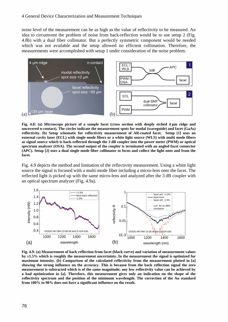
4 General Device Characterization and Measurement Techniques
noise level of the measurement can be as high as the value of reflectivity to be measured. An idea to circumvent the problem of noise from back-reflection would be to use setup 2 (Fig. 4.8b) with a dual fiber collimator. But a perfectly symmetric component would be needed which was not available and the setup allowed no efficient collimation. Therefore, the measurements were accomplished with setup 1 under consideration of the noise problem.
(a) (b) Fig. 4.8: (a) Microscope picture of a sample facet (cross section with deeply etched 4 µm ridge and uncovered n-contact). The circles indicate the measurement spots for modal (waveguide) and facet (GaAs) reflectivity. (b) Setup schematic for reflectivity measurement of AR-coated facet. Setup [1] uses an
facet connector PC). Setup [2] uses a dual single mode fiber collimator to focus and collect the light onto and from the
external cavity laser (ECL) with single mode fibers or a white light source (WLS) with multi mode fibers as signal source which is back-reflected through the 3 dB coupler into the power meter (PWM) or optical spectrum analyzer (OSA). The second output of the coupler is terminated with an angled (Afacet. Fig. 4.9 depicts the method and limitation of the reflectivity measurement. Using a white light source the signal is focused with a multi-mode fiber including a micro-lens onto the facet. The reflected light is picked up with the same micro-lens and analyzed after the 3 dB coupler with an optical spectrum analyzer (Fig. 4.9a).
0.8
1.0
1.2
1.4
1.6
1000 1200 1400 1600
0.4
0.6
DO520 AR FBH 23.08.06 bar2.5 02A-03d
ensi
ty (n
W)
+1.5% facet back reflection -1.5%
0.1
1
int
wavelength(a)1000 1200 1400 1600
1E-3
0.01
(b)
facet refl. +1.5% facet front facet refl. -1.5%
corr. for Au 98% simulation
refle
ctiv
ity R
DO520 AR FBH 23.08.06 bar2.5 02A-03d
wavelength (nm)
F Measurem reflection from k curve) and var easurement values b h is rou easurement unc the measurem nal is optimized for maximum intensity. (b) Comparison of the calc ctivity from th ment plotted in [a] s rong inf the accuracy. T use from the b ion signal the zero m btra is of the same magnitude; any low reflect can be achieved by bad optimization in [a]. Therefore, this measurement gives only an indication on the shape of the
ig. 4.9: (a) ent of back facet (blac iation of my ±1.5% whic ghly the m ertainty. In ent the sig
ulated reflehis is beca
e measureack reflecthowing the st luence on
easurement is su cted which ivity value areflectivity spectrum and the position of the minimum wavelength. The correction of the Au standard from 100% to 98% does not have a significant influence on the result.
76
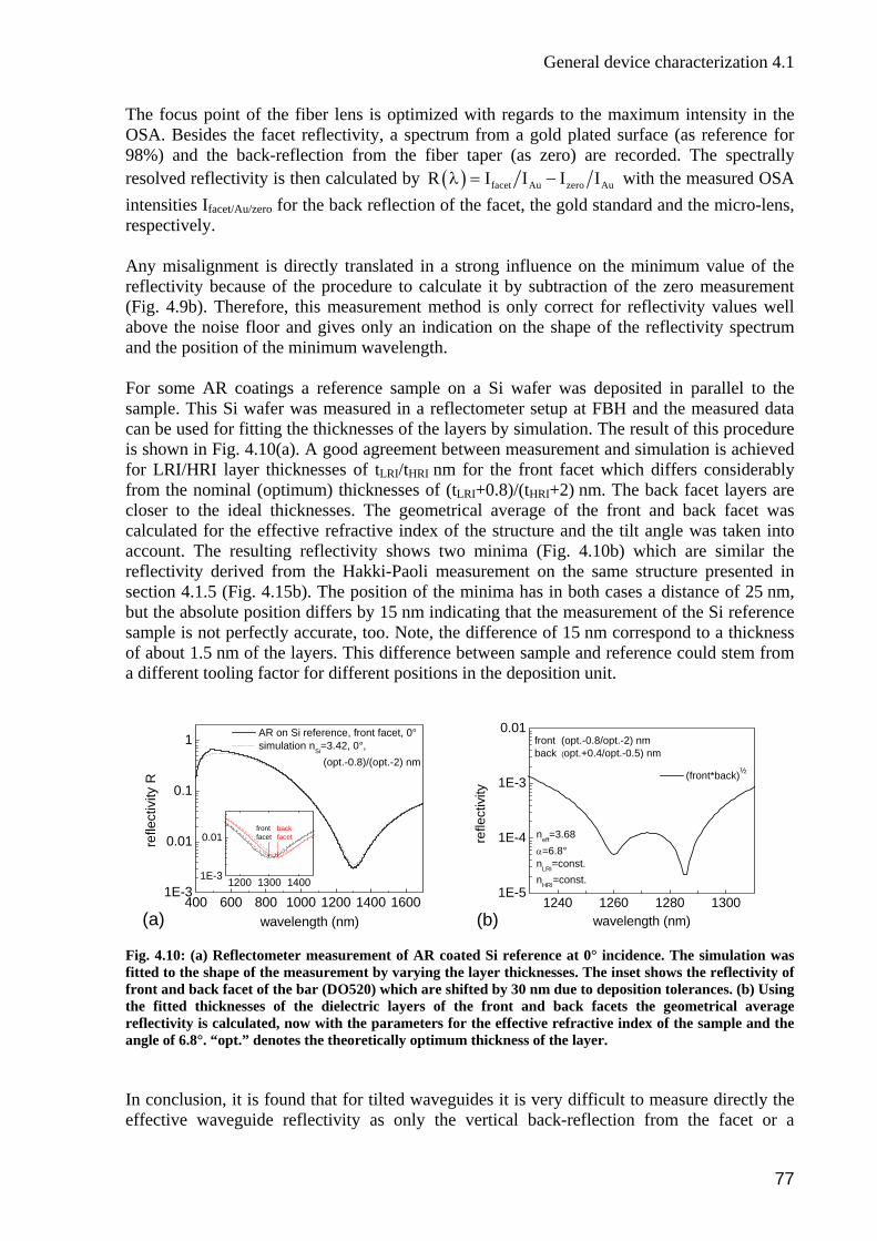
General device characterization 4.1
The focus point of the fiber lens is optimized with regards to the maximum intensity in the A. Besides the facet reflectivity, a spectrum from a gold plated surface (as reference for
) and the back-reflection from the fiber taper (as zero) are recorded. The spectrally lved reflectivity is then calculated by
OS98%reso ( ) facet Au zero AuR I I I Iλ = − with the measured OSA
nsities Ifacet/Au/zero for the back reflection of the facet, the gold standard and the micro-lens, inte
Anyrefl traction of the ze(Fig for re welaboand For some AR coatings a reference samsamcan mulation. The result of this procedure
shown in Fig. 4.10(a). A good agreement between measurement and simulation is achieved r LRI/HRI layer thicknesses of tLRI/tHRI nm for the front facet which differs considerably
rence
f about 1.5 nm of the layers. This difference between sample and reference could stem from
respectively.
misalignment is directly translated in a strong influence on the minimum value of the ectivity because of the procedure to calculate it by sub ro measurement . 4.9b). Therefore, this measurement method is only correct flectivity values l ve the noise floor and gives only an indication on the shape of the reflectivity spectrum the position of the minimum wavelength.
ple on a Si wafer was deposited in parallel to the ple. This Si wafer was measured in a reflectometer setup at FBH and the measured data be used for fitting the thicknesses of the layers by si
isfofrom the nominal (optimum) thicknesses of (tLRI+0.8)/(tHRI+2) nm. The back facet layers are closer to the ideal thicknesses. The geometrical average of the front and back facet was calculated for the effective refractive index of the structure and the tilt angle was taken into account. The resulting reflectivity shows two minima (Fig. 4.10b) which are similar the reflectivity derived from the Hakki-Paoli measurement on the same structure presented in section 4.1.5 (Fig. 4.15b). The position of the minima has in both cases a distance of 25 nm, but the absolute position differs by 15 nm indicating that the measurement of the Si refe
mple is not perfectly accurate, too. Note, the difference of 15 nm correspond to a thickness saoa different tooling factor for different positions in the deposition unit.
1
400 600 800 1000 1200 1400 16001E-3
0.01
0.1
1200 1300 14001E-3
0.01
facetback
front
flect
iv
facetreity
R
wavelength (nm)
AR on Si reference, front facet, 0° simulation nSi=3
0.01.42, 0°,
(opt.-0.8)/(opt.-2) nm
1E-4
1E-3
(a)1240 1260 1280 1300
1E-5
(front*back)½
refle
ctiv
ity
neff=3.68
front (opt.-0.8/opt.-2) nmback (opt.+0.4/opt.-0.5) nm
R coated Si reference at 0° incidence. The simulation was
wavelength (nm)
α=6.8°nLRI=const.nHRI=const.
(b)
ig. 4.10: (a) Reflectometer measurement of AFfitted to the shape of the measurement by varying the layer thicknesses. The inset shows the reflectivity of front and back facet of the bar (DO520) which are shifted by 30 nm due to deposition tolerances. (b) Using the fitted thicknesses of the dielectric layers of the front and back facets the geometrical average reflectivity is calculated, now with the parameters for the effective refractive index of the sample and the angle of 6.8°. “opt.” denotes the theoretically optimum thickness of the layer. In conclusion, it is found that for tilted waveguides it is very difficult to measure directly the effective waveguide reflectivity as only the vertical back-reflection from the facet or a
77
4 General Device Characterization and Measurement Techniques
reference sample can be measured. The effective reflectivity can then be calculated using the reflectivity simulation tool, but with a large error margin.
The information that is contained in the spectral ripple of the emission of the amplifier can be extracted with the Hakki-Paoli method as described in the next section. It is possible to etermine the effective reflectivity indirectly with this method using an additional specd
gtral
ain measurement.
4.1.5 Hakki-Paoli measurement The reflectivities of the facets of a semiconductor device result in a Fabry-Perot-like cavity. In conjunction with the gain of the semiconductor medium this results in a modulation of the emission spectrum of the device. Therefore, the modulation comprises information about the reflectivity and the modal gain of the device – generally speaking this information is accessed
the so-called Hakki-Paoli method [182]with . Determination of the effective index of refraction Due to the facet and sidewall reflectivities the emission spectrum of a laser or an amplifier shows lateral and longitudinal modes. If the device is laterally single mode, then 2Ln m , with m= λ ∈
he wavelength λ defined in vacuum. With holds for the longitudinal modes for a Fabry-Perot cavity of length L,
refractive index n and t m mf c mc 2Ln= λ = , c is the speed of light, we can find the mode distance from
2
m m 1cf f f − 2Ln 2Ln
λ∆ = − = ⇒ ∆λ = . (4.3)
Using the Fresnel formula (7.6) the reflectivity R of an interface air-semiconductor can be calculated under vertical incidence by ) ( ) (2 2
1 2 1 2R n n n n= − + with the refractive index of the semiconductor material n1 and of air n2. This is of course only valid for uncoated facets. The reflectivity of an AR coated facet can be characterized with the Hakki-Paoli method. Derivation of the gain-reflectivity product with the Hakki-Paoli method The spectrum of the spontaneous emission below the lasing threshold is measured in high resolution. The minima P i
minλ and maxima P i
maxλ of the spectrum stem from the destructive and
constructive interference of the lightwave that is being reflected between the facets. From this Fabry-Perot modulated ripple a relation for the gain spectrum can be deduced [182]
( )i i
i i
max mini 1 2
max min
P P1 1g( ) ln ln R RL 2LP P
λ λ
λ λ
⎛ ⎞−⎜ ⎟λ − α = −⎜ ⎟+⎝ ⎠
(4.4)
78
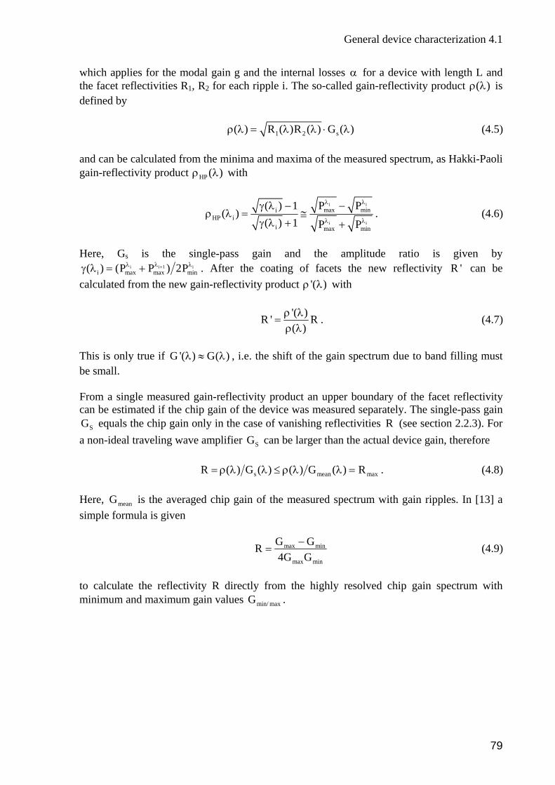
General device characterization 4.1
which applies for the modal gain g and the internal losses α for a device with length L and the facet reflectivities R1, R2 for each ripple i. The so-called gain-reflectivity product ( )ρ λ is defined by 1 2 s( ) R ( )R ( ) G ( )ρ λ = λ λ ⋅ λ (4.5) and can be calculated from the minima and maxima of the measured spectrum, as Hakki-Paoli gain-reflectivity product HP ( )ρ λ with
i i
max miniHP i
i
P P( ) 1( )
( )
λ λ−γ λ −ρ λ = ≅
γ λ +. (4.6)
i imax min
1 P Pλ λ+ Here, Gs is the single-pass gain and the amplitude ratio is given by
i i 1 ii max max min( ) (P P ) 2P+λ λ λγ λ = + . After the coating of facets the new reflectivity R ' can be
calculated from the new gain-reflectivity product '( )ρ λ with
'( )R ' R( )
ρ λ=
ρ λ. (4.7)
This is only true if G '( ) G( )λ ≈ λ , i.e. the shift of the gain spectrum due to band filling must be small. From a single measured gain-reflectivity product an upper boundary of the facet reflectivity can be estimated if the chip gain of the device was measured separately. The single-pass gain
SG equals the chip gain only in the case of vanishing reflectivities R (see section 2.2.3). For n-ideal traveling wave amplifier can be larger than the ac ice gain, therefore
a no SG tual dev
s meanR ( ) G ( ) ( ) G ( ) R= ρ λ λ ≤ ρ λ λ = max . (4.8) Here, is the averaged chip gain of the measured spectrum with gain ripples. In [13] a simple formula is given
meanG
max min
max min
G GR4G G
−= (4.9)
to calculate the reflectivity R directly from the highly resolved chip gain spectrum with
minimum and maximum gain values min/ maxG .
79
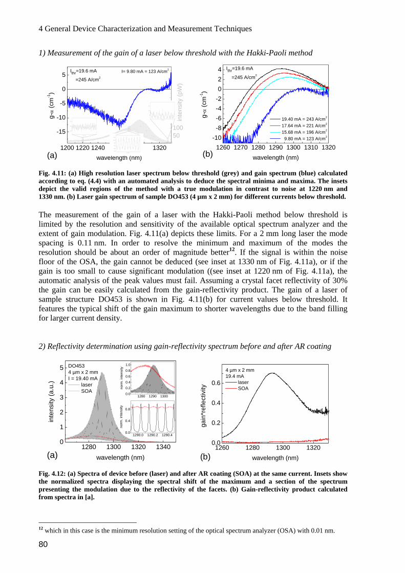
4 General Device Characterization and Measurement Techniques
1) Measurement of the gain of a laser below threshold with the Hakki-Paoli method
1200 1220 1240 1260 1280 1300 1320
-15
-10
-5
0
5
50100150200250300350400450
1220
15
20
25
I= 9.80 mA = 123 A/cm2
(cm
-1)
Ithr=19.6 mA
=245 A/cm2
g-α
wavelength (nm)1280
80
85
90
95
100
105
1340
5
10
15
inte
nsity
(pW
)
(a)1260 1270 1280 1290 1300 1310 1320
-10-8-6-4-2024
(b)
19.40 mA = 243 A/cm2
17.64 mA = 221 A/cm2
15.68 mA = 196 A/cm2
9.80 mA = 123 A/cm2
g-α
(cm
=19.6 mA
he measurement of the gain of a laser with the Hakki-Paoli method below threshold is tical spectrum analyzer and the
its. For a 2 mm long laser the mode
loor of the OSA, the
acet reflectivity oftivity product. The gain of a laser of
ample structure DO453 is shown in Fig. 4.11(b) for current values below threshold. It the typical shift of the gain maximum to shorter wavelen
r larger current density.
ectivity spectrum befo
-1)
thr
=245 A/cm2
I
wavelength (nm)
Fig. 4.11: (a) High resolution laser spectrum below threshold (grey) and gain spectrum (blue) calculated according to eq. (4.4) with an automated analysis to deduce the spectral minima and maxima. The insets depict the valid regions of the method with a true modulation in contrast to noise at 1220 nm and 1330 nm. (b) Laser gain spectrum of sample DO453 (4 µm x 2 mm) for different currents below threshold. Tlimited by the resolution and sensitivity of the available opxtent of gain modulation. Fig. 4.11(a) depicts these lime
spacing is 0.11 nm. In order to resolve the minimum and maximum of the modes the resolution should be about an order of magnitude better12. If the signal is within the noise f gain cannot be deduced (see inset at 1330 nm of Fig. 4.11a), or if the gain is too small to cause significant modulation ((see inset at 1220 nm of Fig. 4.11a), the automatic analysis of the peak values must fail. Assuming a crystal f 30% the gain can be easily calculated from the gain-reflecsfeatures gths due to the band filling fo 2) Reflectivity determination using gain-refl re and after AR coating
5
1280 1300 1320 13400
1
2
3
4
(a)
1290.0 1290.2 1290.40.0
0.4
0.8
nten
sity
norm
. i
1280 1290 13000.0
0.2
0.4
0.6
0.8
1.0
nten
sityDO453
4 µm x 2 mmI = 19.40 mA
norm
. i
laser SOA
u.)
inte
nsity
(a.
wavelength (nm)1260 1280 1300 1320
0.0
0.2
0.4
0.6
4 µm x 2 mm19.4 mA
ectiv
ityga
in*r
efl
wavelength (nm)
laser SOA
ig. 4.12: (a) Spectra of device before (laser) and after AR coating (SOA) at the same current. Insets show
the normalized spectra displaying the spectral shift of the maximum and a section of the spectrum resenting the modulation due to the reflectivity of the facets. (b) Gain-refle
from spectra in [a].
(b)
F
p ctivity product calculated
12 which in this case is the minimum resolution setting of the optical spectrum analyzer (OSA) with 0.01 nm.
80
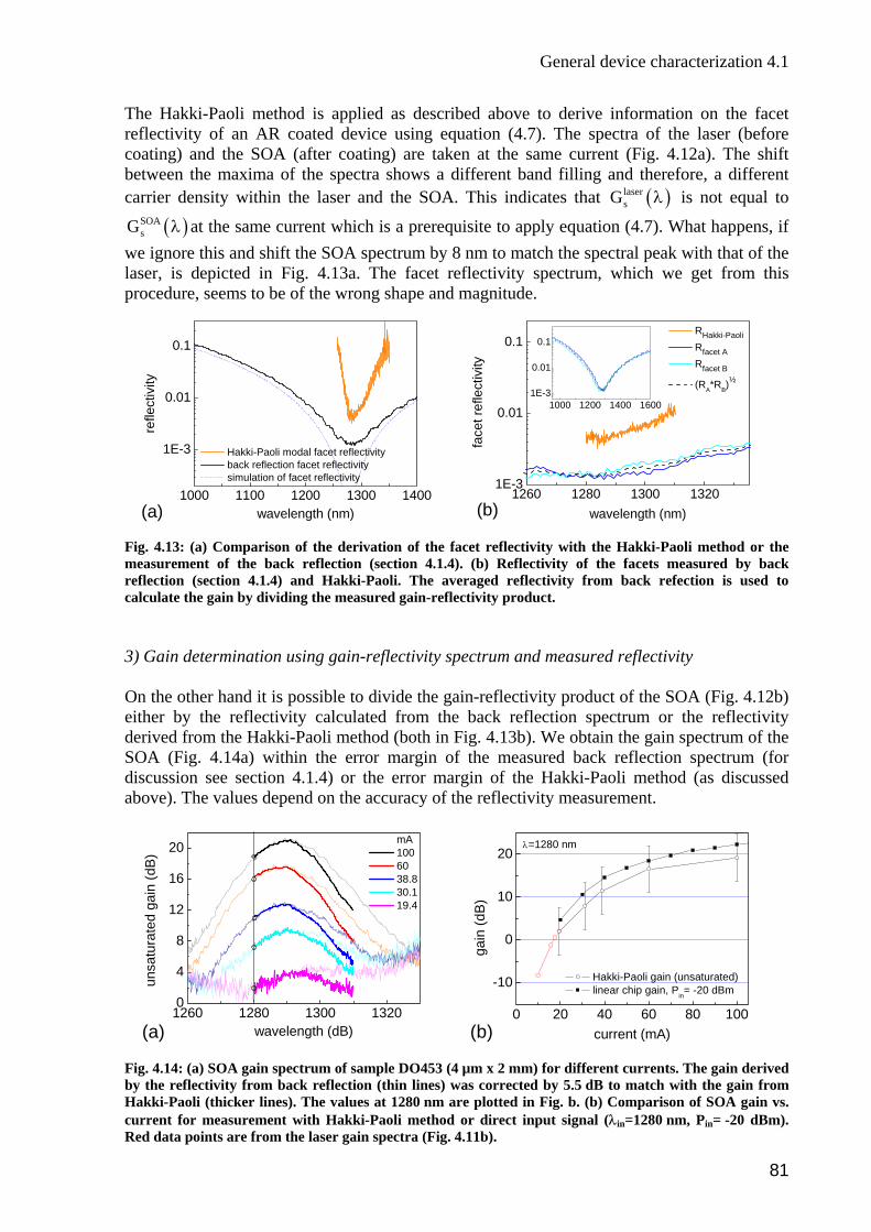
General device characterization 4.1
The Hakki-Paoli method is applied as described above to derive information on the facet reflectivity of an AR coated device using equation (4.7). The spectra of the laser ( re coating) and the SOA (after coatin
befog) are taken at the same current (Fig. 4.12a). The shift
etween the maxima of the spectra shows a different band filling and therefore, a different arrier density within the laser and the SOA. This indicate
λ at the same current which is a prerequisite to apply equation (4.7). What happens, if
. 4.13a facet reflectivity spectrum, which we get from this rocedure, seems to be of the wrong shape and magnitude.
0.1
bc s that ( )laser
sG λ is not equal to
( )SOAsG
we ignore this and shift the SOA spectrum by 8 nm to match the spectral peak with that of the laser, is depicted in Fig . Thep
1000 1100 1200 1300 1400
1E-3
0.01
(a)
Hakki-Paoli modal facet reflectivity back reflection facet reflectivity simulation of facet reflectivity
refle
ct
wavelength (nm)
1E-3
0.1
ivity
0.01
1260 1280 1300 1320
1000 1200 1400 16001E-3
0.01
0.1
(b)
RHakki-Paoli Rfacet A Rfacet B
(RA*RB)
face
t ref
lect ½iv
ity
son of the deriack reflection
section 4.1.4) and Hakki-Paoli. The averaged reflectivity from back refection is used to lculate the gain by dividing the measured gain-reflectivity product.
3)
) ither by the reflectivity calculated from the back reflection spectrum or the reflectivity erived from the Hakki-Paoli method (both in Fig. 4.13b). We obtaOA (Fig. 4.14a) within the error margin of the measured back reflection spectrum (for
16
20
wavelength (nm)
Fig. 4.13: (a) Compari vation of the facet reflectivity with the Hakki-Paoli method or the measurement of the b (section 4.1.4). (b) Reflectivity of the facets measured by back reflection (ca
Gain determination using gain-reflectivity spectrum and measured reflectivity On the other hand it is possible to divide the gain-reflectivity product of the SOA (Fig. 4.12bed in the gain spectrum of the Sdiscussion see section 4.1.4) or the error margin of the Hakki-Paoli method (as discussed above). The values depend on the accuracy of the reflectivity measurement.
1260 1280 1300 13200
4
8
12
atur
ated
ga
uns
in (d
B)
wavelength (dB)
mA 100 60 38.8 30.1
(a)0 20 40 60 80 100
-10
0
10
20
Hakki-Paoli gain (unsaturated) linear chip gain, Pin= -20 dBm
19.4
gain
(dB
)
current (mA)
λ=1280 nm
(b)
ig. 4.14: (a) SOA gain spectrum of sample DO453 (4 µm x 2 mm) for different currents. The gain derived y the reflectivity from back reflection (thin lines) was corrected by 5.5 dB to match with the gain from akki-Paoli (thicker lines). The values at 1280 nm are plotted in Fig. b. (b) Comparison of SOA gain vs. rrent for measurement with Hakki-Paoli method or direct input signal (λin=1280 nm, Pin= -20 dBm).
ed data points are from the laser gain spectra (Fig. 4.11b).
FbHcuR
81
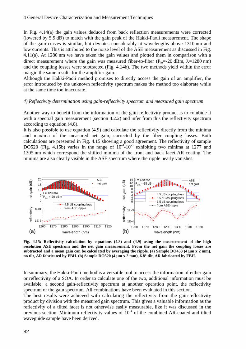
4 General Device Characterization and Measurement Techniques
In Fig. 4.14(a) the gain values deduced from back reflection measurements were corrected (lowered by 5.5 dB) to match with the gain peak of the Hakki-Paoli measurement. The shape of the gain curves is similar, but deviates considerably at wavelengths above 1310 nm and low currents. This is attributed to the noise level of the ASE measurement as discussed in Fig. 4.11(a). At 1280 nm we have taken the gain values and plotted them in comparison with a direct measurement where the gain was measured fiber-to-fiber (Pin=-20 dBm, λ=1280 nm) and the coupling losses were subtracted (Fig. 4.14b). The two methods yield within the error margin the same results for the amplifier gain. Although the Hakki-Paoli method promises to directly access the gain of an amplifier, the error introduced by the unknown reflectivity spectrum makes the method too elaborate while at the same time too inaccurate. 4) Reflectivity determination using gain-reflectivity spectrum and measured gain spectrum
ccording to equation (4.8).
Another way to benefit from the information of the gain-reflectivity product is to combine it with a spectral gain measurement (section 4.2.2) and infer from this the reflectivity spectrum aIt is also possible to use equation (4.9) and calculate the reflectivity directly from the minima and maxima of the measured net gain, corrected by the fiber coupling losses. Both calculations are presented in Fig. 4.15 showing a good agreement. The reflectivity of sample DO520 (Fig. 4.15b) varies in the range of 10-4-10-3 exhibiting two minima at 1277 and 1305 nm which correspond the shifted minima of the front and back facet AR coating. The minima are also clearly visible in the ASE spectrum where the ripple nearly vanishes.
0
5
10
15
20
1260 1270 1280 1290 1300 1310 1320
1E-3
0.01
net g
ain
(dB
) ASE net gain
I = 120 mAP =-20 dBm
02468
101214
1260 1270 1280 1290 1300 1310 1320
1E-4
ECL
4.5 dB coupling loss from ASE-ripple
ectiv
ity
wavelength (nm)
refl
(a)
1E-3
t gai
n (d
B)ne
ASE net gain
I = 120 mAPECL=-15 dBm
4.5 dB coupling loss 5.5 dB coupling loss 6.5 dB coupling loss from ASE-ripple
refle
ct
wavelength (nm)
ivity
(b)
Fig. 4.15: Reflectivity calculation by equations (4.8) and (4.9) using the measurement of the high resolution ASE spectrum and the net gain measurement. From the net gain the coupling losses are subtracted and a mean gain can be calculated by averaging the ripple. (a) Sample DO453 (4 µm x 2 mm), no tilt, AR fabricated by FBH. (b) Sample DO520 (4 µm x 2 mm), 6.8° tilt, AR fabricated by FBH. In summary, the Hakki-Paoli method is a versatile tool to access the information of either gain or reflectivity of a SOA. In order to calculate one of the two, additional information must be available: a second gain-reflectivity spectrum at another operation point, the reflectivity
flectivity of a tilted facet is not otherwise easily measurable, like it was discussed in the previous section. Minimum reflectivity values of 10-4 of the combined AR-coated and tilted waveguide sample have been derived.
spectrum or the gain spectrum. All combinations have been evaluated in this section. The best results were achieved with calculating the reflectivity from the gain-reflectivity product by division with the measured gain spectrum. This gives a valuable information as the re
82
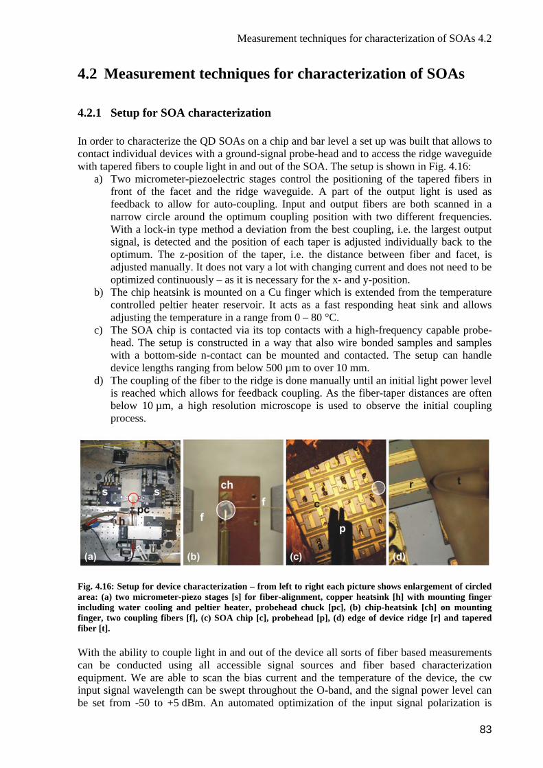
Measurement techniques for characterization of SOAs 4.2
4.2 Measurement techniques for characterization of SOAs
4.2.1 Setup for SOA characterization
to characterize the QD SOAs on a chip and bar level a set up was built that allows to contact individual devices with a ground-signal probe-head and to access the ridge waveguide with tapered fibers to couple light in and out of the SOA. The setup is shown in Fig. 4.16:
a) Two micrometer-piezoelectric stages control the positioning of the tapered fibers in front of the facet and the ridge waveguide. A part of th
In order
e output light is used as feedback to allow for auto-coupling. Input and output fibers are both scanned in a narrow circle around the optimum coupling position with two different frequencies. With a lock-in type method a deviation from the best coupling, i.e. the largest output signal, is detected and the position of each taper is adjusted individually back to the optimum. The z-position of the taper, i.e. the distance between fiber and facet, is adjusted manually. It does not vary a lot with changing current and does not need to be optimized continuously – as it is necessary for the x- and y-position.
b) The chip heatsink is mounted on a Cu finger which is extended from the temperature controlled peltier heater reservoir. It acts as a fast responding heat sink and allows adjusting the temperature in a range from 0 – 80 °C.
c) The SOA chip is contacted via its top contacts with a high-frequency capable probe
an initial light power level is reached which allows for feedback coupling. As the fiber-taper distances are often
al coupling
-head. The setup is constructed in a way that also wire bonded samples and samples with a bottom-side n-contact can be mounted and contacted. The setup can handle device lengths ranging from below 500 µm to over 10 mm.
d) The coupling of the fiber to the ridge is done manually until
below 10 µm, a high resolution microscope is used to observe the initiprocess.
Fig. 4.16: Setup for device characterization – from left to right each picture shows enlargement of circled area: (a) two micrometer-piezo stages [s] for fiber-alignment, copper heatsink [h] with mounting finger including water cooling and peltier heater, probehead chuck [pc], (b) chip-heatsink [ch] on mounting finger, two coupling fibers [f], (c) SOA chip [c], probehead [p], (d) edge of device ridge [r] and tapered fiber [t]. With the ability to couple light in and out of the device all sorts of fiber based measurements can be conducted using all accessible signal sources and fiber based characterization equipment. We are able to scan the bias current and the temperature of the device, the cw input signal wavelength can be swept throughout the O-band, and the signal power level can be set from -50 to +5 dBm. An automated optimization of the input signal polarization is
83
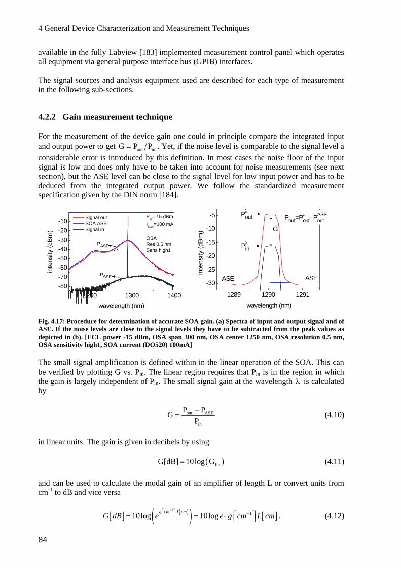
4 General Device Characterization and Measurement Techniques
available in the fully Labview [183] implemented measurement control panel which operates all equipment via general purpose interface bus (GPIB) interfaces. The signal sources and analysis equipment used are described for each type of measurement in the following sub-sections.
4.2.2 Gain measurement technique For the measurement of the device gain one could in principle compare the integrated input and output power to get outG P= inP . Yet, if the noise level is comparable to the signal level a onsiderable error is introduced by this definition. In most cases the noise floor of the input
xt csignal is low and does only have to be taken into account for noise measurements (see nesection), but the ASE level can be close to the signal level for low input power and has to be deduced from the integrated output power. We follow the standardized measurement specification given by the DIN norm [184].
1200 1300 1400-80-70-60
1289 1290 1291
-30
-25
-20
-15
-10
-5 Pout=Pλout- P
ASEout
sity
(dB
m)
ASE inte
n
wavelength (nm)
ASE
Pλout
Pλin
G
PSSE
wavelength (nm)
-50-40-30-20-10
inte
nsity
(dB
m)
Signal out SOA ASE Signal in
Pin=-15 dBmISOA=100 mA
OSARes 0.5 nmSens high1
PASE
Fig. 4.17: Procedure for determination of accurate SOA gain. (a) Spectra of input and output signal and of ASE. If the noise levels are close to the signal levels they have to be subtracted from the peak values as depicted in (b). [ECL power -15 dBm, OSA span 300 nm, OSA center 1250 nm, OSA resolution 0.5 nm, OSA sensitivity high1, SOA current (DO520) 100mA] The small signal amplification is defined within in the linear operation of the SOA. This can be verified by plotting G vs. Pin. The linear region requires that Pin is in the region in which the gain is largely independent of Pin. The small signal gain at the wavelength is calculateλ d by
out ASEP PGPin
−= (4.10)
in linear units. The gain is given in decibels by using ( )linG[dB] 10log G= (4.11) and can be used to calculate the modal gain of an amplifier of length L or convert units from cm-1 to dB and vice versa
[ ] [ ]( ) [ ]1
110log−⎡ ⎤⋅ −⎣ ⎦ ⎡ ⎤= = ⋅
g cm L cmG dB e 10log ⎣ ⎦e g cm L cm . (4.12)
84

Measurement techniques for characterization of SOAs 4.2
he measurement principle is depicted in Fig. 4.17 where the associated signal levels oT
sof the
urce spontaneous emission (SSE), ASE, input and output signal are plotted vs. wavelength. spectrum of the output signal – such as the
ted for signal and ASE level.
Formethod
•
•
Usually, for each gain measurement data point a red graph in Fig. 4.17(b) – is taken and evalua
4.2.3 Noise measurement technique
a quantitative measure the noise figure of a SOA (chapter 2.2.5) can be evaluated by two s:
Using an optical spectrum analyzer (OSA) to measure the gain and the spectrally resolved ASE to calculate the noise figure terms of equation (2.35) except the noise contribution from multi path interference. Measuring the electronic noise with an electrical spectrum analyzer (ESA) and a broadband optical photodetector to evaluate the total noise figure including the multi path interference term. Note: this part is strongly dependent on the base frequency, linewidth of the source and polarization match of the multiple reflections.
1288 1289 1290 1291 1292-30
-25 PASEoutPASE
out 1PASE
out 2
-20
-15
-10
-5
0Pout=Pλ
out- PASEout
(dB
m) Pλ
out
OSA RBW 1nm
tput
pow
er
ou
wavelength (nm)
Fig. 4.18: Procedure for determination of accurate signal power from OSA measurement: Interpolation of the ASE levels and subtraction of this value from the peak power. (Here shown for the output power levels. Same procedure applies for input signal with signal spontaneous emission power). Optical spectrum analyzer method There are two alternate ways [185] to determine the signal-spontaneous noise figure with an OSA: the method of direct ASE-interpolation (DI) and the polarization extinction with
terpolation method. Although the DI method has some limitations for a strongly wavelength independent ASE spectral gradient and for large signal input power it is used here for its simpler setup and its satisfactory accuracy. The noise factor is calculated according to
ASE SSE
0 0
P P1NGh B G h B
= + −ν ν
(4.13)
with the last term performing a subtraction of the amplified signal spontaneous emission SSEP . As the measurement of ASEP and SSEP at the signal wavelength is not possible due to the presence of the signal peak, interpolation is required to estimate the noise powers at the signal
85
4 General Device Characterization and Measurement Techniques
wavelength (Fig. 4.18). A detailed discussion on the calibration of the OSA and the determination of resolution bandwidth for this measurement is found in the technical nnex 7.2.
ethod
With this method [186] the electrical noise is measured directly using a modulated signal that zed in an electrical spectrum analyzer. It is based
traight on the definition of the noise factor including all relevant noise contributions
atch of the
The coupling efficiency between the amplifier and the coupling fibers is very important for the noise figure. With P one can describe the signal output power of the amplifier under consider
a Electrical spectrum analyzer m
is amplified with the SOA and characteris(chapter 2.2.5). Yet, it is strongly dependent on the base frequency, linewidth of the source signal and polarization m multiple reflections, which makes the method delicate in handling and interpreting of the results. As all necessary information for the optical spectrum analyzer method is collected in our standard gain measurement we have not applied the ESA method to determine the noise factor. Influence of coupling efficiency on noise figure
out 1 2 inP G= η ηation of the input 1η and output 2η coupling efficiencies,
respectively. For the ASE output power in fiber we use 2 ASEPη and thus, the signal-to-ASE ratio out 1 2 in 2 ASE 1 in ASESNR GP P G P P= η η η = η . (4.14) This shows that the output SNR is only dependent on the input coupling efficiency13. In order
.3.1 Amplification of mode-locked laser pulse trains
The setup of this measurement is described in the context of the experiment in section 5.2.1.
.3.2 Double pump- and probe setup
he gain dynamics in the amplifier are measured in collaboration with the group of U.
te Ti:Sapphire laser, tunable pump and probe pulses are
to realize a low-noise fiber-to-fiber coupled SOA it is important to reduce the input coupling loss. 4.3 Dynamic characterization techniques
4
4 TWoggon, Universität Dortmund, by a femtosecond pump-probe technique with heterodyne detection as described in [187, 188] (see Fig. 4.19). Using an optical parametric oscillator umped by a 75 MHz repetition rap
13 The input SNR is - by definition - independent of the coupling efficiency as it is measured before the coupling.
86
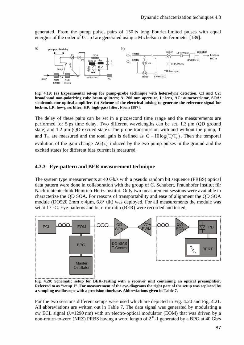
Dynamic characterization techniques 4.3
generated. From the pump pulse, pairs of 150 fs long Fourier-limited pulses with equal energies of the order of 0.1 pJ are generated using a Michelson interferometer [189].
ig. 4.19: (aFb
) Experimental set-up for pump-probe technique with heterodyne detection. C1 and C2: ro a
sem nlock-in. The eperformstate) aand T0
adb nd non-polarizing cube beam-splitters; A: 200 mm aperture, L: lens, AC: autocorrelator, SOA: ico ductor optical amplifier. (b) Scheme of the electrical mixing to generate the reference signal for
LP: low-pass filter, HP: high-pass filter. From [187].
d lay of these pairs can be set in a picosecond time range and the measurements are ed for 5 ps time delay. Two different wavelengths can be set, 1.3 µm (QD ground
nd 1.2 µm (QD excited state). The probe transmission with and without the pump, T , are measured and the total gain is defined as ( )0G 10log T T= . Then the temporal
volution of the gain change induced by the two pump pulses in the ground and the excited states for different bias current is measured.
4.3.3 Eye-pattern and BER measurement technique The system type measurements at 40 Gb/s with a pseudo random bit sequence (PRBS) optical data pattern were done in collaboration with the group of C. Schubert, Fraunhofer Institut für Nachrichtentechnik Heinrich-Hertz-Institut. O wo measurement sessions were available to characterize the QD SOA. For reasons of transportability and ease of alignment the QD SOA module (DO520 2mm x 4µm, 6.8° tilt) was deployed. For all measurements the module was set at 17 °C. Eye-patterns and bit error ratio (BER) were recorded and t
e G( )∆ τ
nly t
ested.
F it containing an optical preamplifier. R right part of the setup was replaced by
ig. 4.20: Schematic setup for BER-Testing with a receiver uneferred to as “setup 1”. For measurement of the eye-diagrams the
oscilloscope with a precision timebase. Abbreviations given in Table 7.
non-return-to-zero (NRZ) PRBS having a word length of 2 -1 generated by a BPG at 40 Gb/s
a sampling For the two sessions different setups were used which are depicted in Fig. 4.20 and Fig. 4.21. All abbreviations are written out in Table 7. The data signal was generated by modulating a cw ECL signal (λ=1290 nm) with an electro-optical modulator (EOM) that was driven by a
31
87

4 General Device Characterization and Measurement Techniques
of the master oscillator. The amplified signal was either recorded by a sampling oscilloscope with a precision timebase (Agilent Infiniium DCA 86100B, 86107A, 86118A) for the eye-diagram or tested with a SHF EA44 BERT for evaluation of the BER.
ue to sensitivity problems on the receiver side – because of the QD SOA operating at a
e characteristics of the setup without the QD SOA.
ration, but the BER deteriorated to a minimum value of only 10 . Comparing the ye-diagrams for both configurations showed also a better eye opening and jitter with the QD
surement was
reduced by the use of an electrical broadband amplifier in front of the BERT. A constant put power of -1 dBm was amplified to +4.8 dBm, i.e. the QD SOA was also working in the
aturation regime.
Setup 1 Dwavelength of 1.3 µm while the setup is optimized for 1.55 µm - an optical preamplifier (QW SOA) was used. The QD SOA was driven in polarization optimized booster configuration, i.e. directly following the modulator with -5.8 dBm constant input power amplified to +2.4 dBm by the QD SOA, i.e. the SOA was working in the saturation regime. The amplified pulses were attenuated by adjusting a VOA to set the receiver optical power. A back-to-back measurement is necessary to evaluate thThis was done by extracting the QD SOA and setting the input power at the QW SOA at the same level as before. One would expect an improvement of the BER in the back-to-back configu 14 -4
eSOA. Setup 2 As the back-to-back mea not feasible with setup 1 we used a modified scheme during the second session. Here the cw signal of the ECL was boosted with a QW SOA to compensate for losses in the EOM and have a larger modulated signal available that could be adjusted by the VOA in front of the QD SOA. The sensitivity problems on the receiver side were ins
Fig. 4.21: “Setup 2” allows adjustment of input power, additionally, only the QD SOA influences the high
eed optical properties. Abbreviations given in Table 7.
sp
14 This is possibly due to a back-reflection of the signal in the system, deteriorating the EOM which has an automatic bias point control.
88
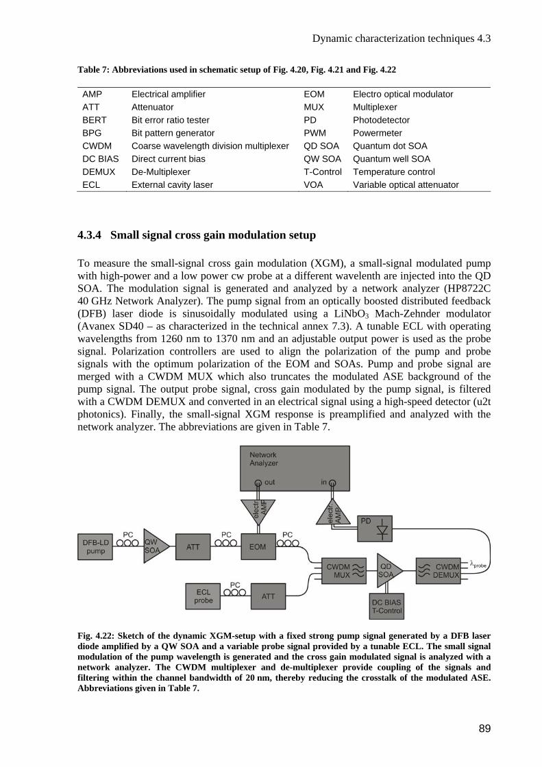
Dynamic characterization techniques 4.3
Table 7: Abbreviations used in schematic setup of Fig. 4.20, Fig. 4.21 and Fig. 4.22 AMP Electrical amplifier EOM Electro optical modulator ATT Attenuator MUX Multiplexer BERT Bit error ratio tester PD Photodetector BPG Bit pattern generator PWM Powermeter CWDM Coarse wavelength division multiplexer QD SOA Quantum dot SOA DC BIAS Direct current bias QW SOA Quantum well SOA DEMUX De-Multiplexer T-Control Temperature control ECL External cavity laser VOA Variable optical attenuator
4.3.4 Small signal cross gain modulation setup To measure the small-signal cross gain modulation (XGM), a small-signal modulated pump with high-power and a low power cw probe at a different wavelenth are injected into the QD SOA. The modulation signal is generated and analyzed by a network analyzer (HP8722C 40 GHz Network Analyzer). The pump signal from an optically boosted distributed feedback (DFB) laser diode is sinusoi modulated using a LiNbO3 Mach-Zehnder modulator (Avanex SD40 – as characterized in the technical annex 7.3). A tunable ECL with operating
avelengths from 1260 nm to 1370 nm and an adju
dally
stable output power is used as the probe gnal. Polarization controllers are used to align the polarization of the pump and probe
As. Pump and probe signal are ulated ASE background of the
ump signal. The output probe signal, cross gain modulated by the pump signal, is filtered
wsisignals with the optimum polarization of the EOM and SOmerged with a CWDM MUX which also truncates the modpwith a CWDM DEMUX and converted in an electrical signal using a high-speed detector (u2t photonics). Finally, the small-signal XGM response is preamplified and analyzed with the network analyzer. The abbreviations are given in Table 7.
Fig. 4.22: Sketch of the dynamic XGM-setup with a fixed strong pump signal generated by a DFB laser diode amplified by a QW SOA and a variable probe signal provided by a tunable ECL. The small signal
odulation of the pump wavelength is generated and the cross gain modulated signal is analyzed with a mnetwork analyzer. The CWDM multiplexer and de-multiplexer provide coupling of the signals and filtering within the channel bandwidth of 20 nm, thereby reducing the crosstalk of the modulated ASE. Abbreviations given in Table 7.
89
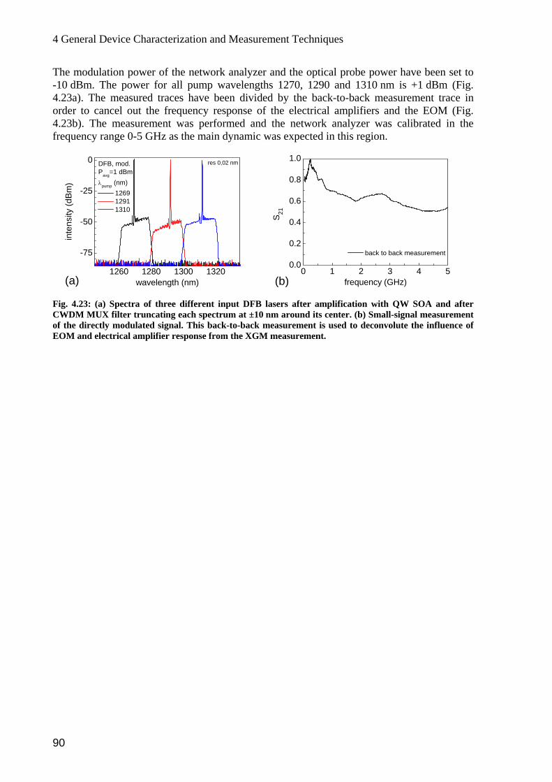
4 General Device Characterization and Measurement Techniques
The modulation power of the network analyzer and the optical probe power have been set to -10 dBm. The power for all pump wavelengths 1270, 1290 and 1310 nm is +1 dBm (Fig. 4.23a). The measured traces have been divided by the back-to-back measurement trace in rder to cancel out the frequency response of the electrical amplifiers and the EOM (Fig.
he measurement was performed and the network analyzer was calibrated in the o4.23b). Tfrequency range 0-5 GHz as the main dynamic was expected in this region.
1260 1280 1300 1320
-75
-50
-25
0
inte
nsity
(dB
m)
DFB, mod.Pavg=1 dBmλpump (nm)
wavelength (nm)
1269 1291 1310
res 0,02 nm
(a)0 1 2 3 4 5
0.0
0.2
0.4
0.6
0.8
1.0
back to back measurement
S 21frequency (GHz)(b)
(a) Spectra of three different input DFB lasers after amplification with QW SOA and after Fig. 4.23:
CWDM MUX filter truncating each spectrum at ±10 nm around its center. (b) Small-signal measurement of the directly modulated signal. This back-to-back measurement is used to deconvolute the influence of EOM and electrical amplifier response from the XGM measurement.
90
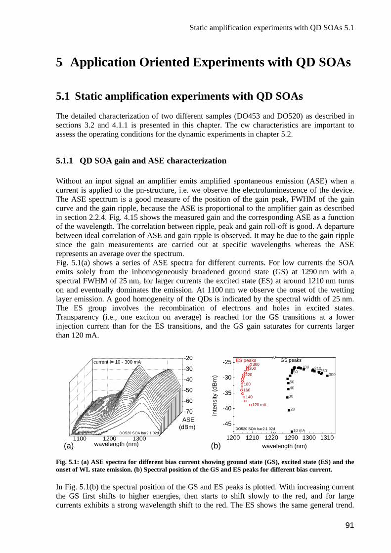
Static amplification experiments with QD SOAs 5.1
5 Application Oriented Experiments with QD SOAs 5 The detailed characterization of two different samples (DO453 and DO520) as described in sections 3.2 and 4.1.1 is presented in this chapte portant to assess the operating conditions for the dynamic exp nts in
5.1.1 QD SOA gain and ASE characterization
ithout an input signal an amplifier emits amplified spontaneous emission (ASE) when a
ns and holes in excited states. ransparency (i.e., one exciton on average) is reached for the GS transitions at a lower
injection current than for the ES transitions, and the GS gain saturates for currents larger than 120 mA.
.1 Static amplification experiments with QD SOAs
r. The cw characteristics are imerime chapter 5.2.
Wcurrent is applied to the pn-structure, i.e. we observe the electroluminescence of the device. The ASE spectrum is a good measure of the position of the gain peak, FWHM of the gain curve and the gain ripple, because the ASE is proportional to the amplifier gain as described in section 2.2.4. Fig. 4.15 shows the measured gain and the corresponding ASE as a function of the wavelength. The correlation between ripple, peak and gain roll-off is good. A departure between ideal correlation of ASE and gain ripple is observed. It may be due to the gain ripple since the gain measurements are carried out at specific wavelengths whereas the ASE represents an average over the spectrum. Fig. 5.1(a) shows a series of ASE spectra for different currents. For low currents the SOA emits solely from the inhomogeneously broadened ground state (GS) at 1290 nm with a spectral FWHM of 25 nm, for larger currents the excited state (ES) at around 1210 nm turns on and eventually dominates the emission. At 1100 nm we observe the onset of the wetting layer emission. A good homogeneity of the QDs is indicated by the spectral width of 25 nm. The ES group involves the recombination of electroT
1100 1200 1300
-70
-60
-50
-40
-30
-20
wavelength (nm)
DO520 SOA bar2.1 02d
current I= 10 - 300 mA
ASE(dBm)
(a)1200 1210 1220 1290 1300 1310
-45
-40
-35
-30
-25 300260
220
180160
140
120 mA
300250210180
80
5040
30
20
10 mADO520 SOA bar2.1 02d
inte
nsity
(dBm
)
wavelength (nm)
ES peaks GS peaks
(b)
Fig. 5.1: (a) ASE spectra for different bias current showing ground state (GS), excited state (ES) and the onset of WL state emission. (b) Spectral position of the GS and ES peaks for different bias current. In Fig. 5.1(b) the spectral position of the GS and ES peaks is plotted. With increasing current the GS first shifts to higher energies, then starts to shift slowly to the red, and for large urrents exhibits a strong wavelength shift to the red. The ES shows the same general trend. c
91
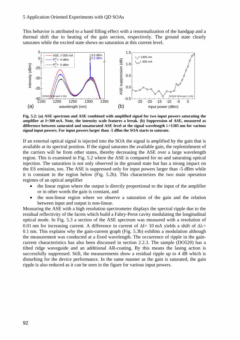
5 Application Oriented Experiments with QD SOAs
This behavior is attributed to a band filling effect with a renormalization of the bandgap and a thermal shift due to heating of the gain section, respectively. The ground state clearly saturates while the excited state shows no saturation at this current level.
0
5
1150 1200 1250 1300 1350-40
-35
-30
-25
DO520 SOA bar2.1 02d
inte
nsity
(dBm
)
wavelength (nm)
3.5 dBm0.2 dBm
1.5 ASE, I=300 mA Ptpr
in = -5 dBm
-25 -20 -15 -10 -5 0-0.5
0.0
0.5
1.0 Ptprin = 0 dBm
(a) (b)
DO520 SOA bar2.1 02d
ASE
sup
pres
sion
input power (dBm)
Fig. 5.2: (a) ASE spectrum and ASE combined with amplified signal for two input powers saturating the amplifier at I=300 mA. Note, the intensity scale features a break. (b) Suppression of ASE, measured as difference between saturated and unsaturated ASE level at the signal wavelength λ=1305 nm for various
lable gain, the replenishment of the carriers will be from other states, thereby decreasing the ASE over a large wavelength region. This is examined in Fig. 5.2 where the ASE is compared for no and saturating optical injection. The saturation is not only observed in the ground state but has a strong impact on the ES emission, too. The ASE is suppressed only for input powers larger than -5 dBm while it is constant in the region below (Fig. 5.2b). This characterizes the two main operation regimes of an optical amplifier
• the linear region where the output is directly proportional to the input of the amplifier or in other words the gain is constant, and
• the non-linear region where we observe a saturation of the gain and the relation between input and output is non-linear.
Measuring the ASE with a high resolution spectrometer displays the spectral ripple due to the residual reflectivity of the facets which build a Fabry-Perot cavity modulating the longitudinal optical mode. In Fig. 5.3 a section of the ASE spectrum was measured with a resolution of 0.01 nm for increasing current. A difference in current of ∆I= 10 mA yields a shift of ∆λ= 0.1 nm. This explains why the gain-current graph (Fig. 5.3b) exhibits a modulation although the measurement was conducted at a fixed wavelength. The occurrence of ripple in the gain-current characteristics has also been discussed in section 2.2.3. The sample (DO520) has a tilted ridge waveguide and an additional AR-coating. By this means the lasing action is successfully suppressed. Still, the measurements show a residual ripple up to 4 dB which is disturbing for the device performance. In the same manner as the gain is saturated, the gain ripple is also reduced as it can be seen in the figure for various input powers.
(dB)
λin= 1305 nmISOA= 300 mA
signal input powers. For input powers larger than -5 dBm the SOA starts to saturate. If an external optical signal is injected into the SOA the signal is amplified by the gain that is available at its spectral position. If the signal saturates the avai
92
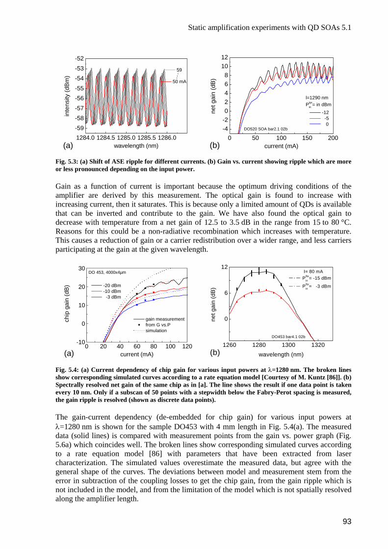
Static amplification experiments with QD SOAs 5.1
1012
1284.0 1284.5 1285.0 1285.5 1286.0-59-58-57-56-55-54-53-52
59
50 mA
tens
Bm
)
wavelength (nm)
ity (d
in
(a)
68
0 50 100-4-20
150 200
24
-12 -5 0
ne
DO520 SOA bar2.1 02b
(dB
)
current (mA)
90 nmPtpr
in = in dBm
(b)
vs. current showing ripple which are more r less pronounced depending on the input power.
t gai
n
l=12
Fig. 5.3: (a) Shift of ASE ripple for different currents. (b) Gaino Gain as a function of current is important because the optimum driving conditions of the amplifier are derived by this measurement. The optical gain is found to increase with increasing current, then it saturates. This is because only a limited amount of QDs is available that can be inverted and contribute to the gain. We have also found the optical gain to decrease with temperature from a net gain of 12.5 to 3.5 dB in the range from 15 to 80 °C. Reasons for this could be a non-radiative recombination which increases with temperature. This causes a reduction of gain or a carrier redistribution over a wider range, and less carriers participating at the gain at the given wavelength.
0 20 40 60 80 100 120-10
0
10
20
30
gain measurement from G vs.P simulation
-20 dBm -10 dBm -3 dBm
chip
gai
n (d
B)
DO 453, 4000x4µm
0
6
12
1260 1280 1300 1320
net g
ain
(dB
)
I= 80 mA
wavelength (nm)
DO453 bar4.1 02b
Pfbrin = -15 dBm
Pfbrin = -3 dBm
current (mA)(a) (b)
Fig. 5.4: (a) Current dependency of chip gain for various input powers at λ=1280 nm. The broken lines show corresponding simulated curves according to a rate equation m del [Courtesy of M. Kuntz [86]]. (b) Spectrally resolved net gain of the same chip as in [a]. The line sh ult if one data point is taken every 10 nm. Only if a subscan of 50 points with a stepwidth below the Fabry-Perot spacing is measured, the gain ripple is resolved (shown as discrete data points). The gain-current dependency (de-embedded for chip gain) for various input powers at λ=1280 nm is shown for the sample DO453 with 4 mm length in Fig. 5.4(a). The measured data (solid lines) is compared with measurement points from the gain vs. power graph (Fig. 5.6a) which coincides well. The broken lines show corresponding simulated curves according
the
oows the res
to a rate equation model [86] with parameters that have been extracted from laser characterization. The simulated values overestimate the measured data, but agree with the eneral shape of the curves. The deviations between model and measurement stem fromg
error in subtraction of the coupling losses to get the chip gain, from the gain ripple which is not included in the model, and from the limitation of the model which is not spatially resolved along the amplifier length.
93
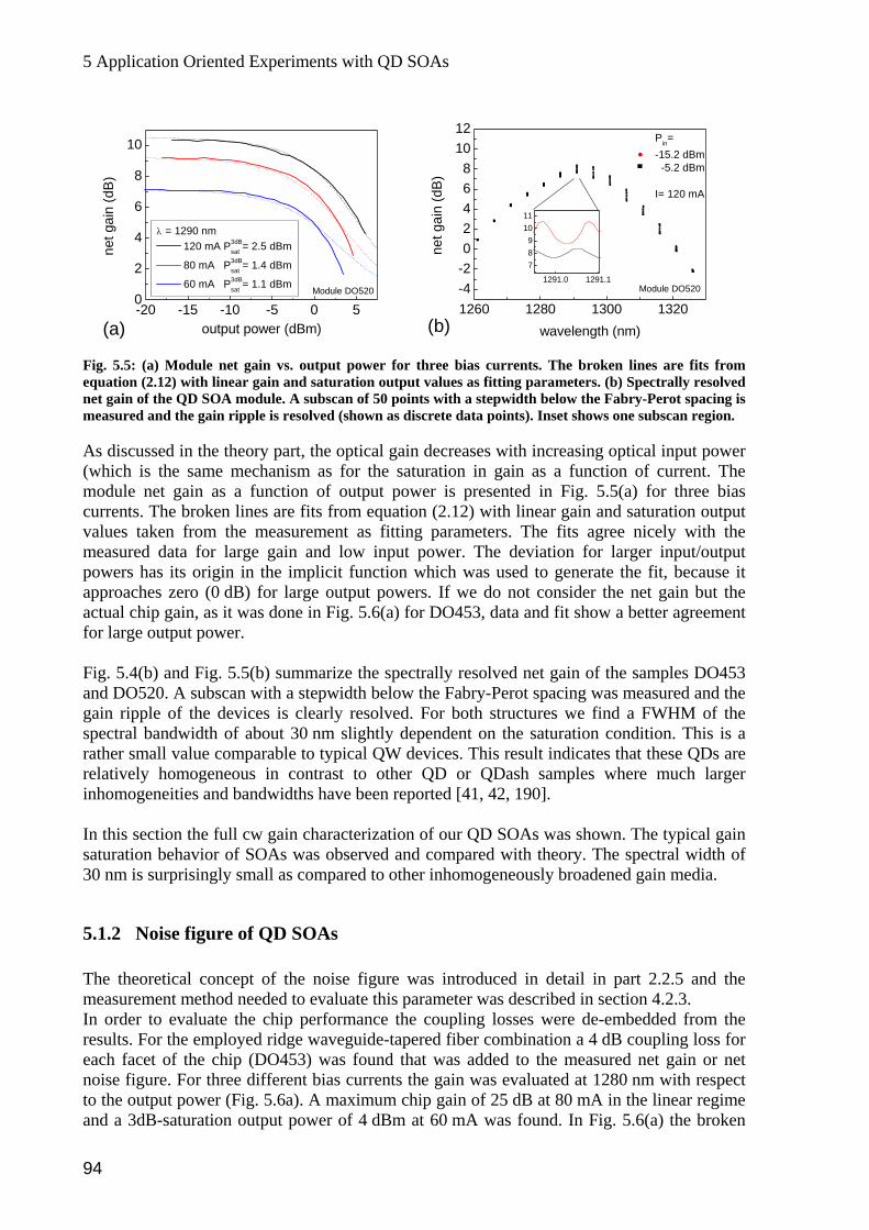
5 Application Oriented Experiments with QD SOAs
1012
-20 -15 -10 -5 0 50
2
4
6
8
10
Module DO520
λ = 1290 nm 120 mA P3dB
sat = 2.5 dBm
80 mA P3dBsat = 1.4 dBm
60 mA P3dBsat = 1.1 dBm
net g
ain
(dB
)
output power (dBm)(a)1260 1280 1300 1320-4-202468
1291.0 1291.1
789
1011
Pin= -15.2 dBm -5.2 dBm
I= 120 mA
Module DO520
net g
ain
(dB
)
wavelength (nm)
(b)
Fig. 5.5: (a) Module net gain vs. output power for three bias currents. The broken lines are fits from equation (2.12) with linear gain and saturation output values as fitting parameters. (b) Spectrally resolved net gain of the QD SOA module. A subscan of 50 points with a stepwidth below the Fabry-Perot spacing is
of current. The odule net gain as a function of output power is presented in Fig. 5.5(a) for three bias
Fig .4and DO Fabry-Perot spacing was measured and the gai ispectra endent on the saturation condition. This is a
The theoretical concept of the noise figure was introduced in detail in part 2.2.5 and the measurement method needed to evaluate this parameter was described in section 4.2.3. In order to evaluate the chip performance the coupling losses were de-embedded from the results. For the employed ridge waveguide-tapered fiber combination a 4 dB coupling loss for each facet of the chip (DO453) was found that was added to the measured net gain or net noise figure. For three different bias currents the gain was evaluated at 1280 nm with respect to the output power (Fig. 5.6a). A maximum chip gain of 25 dB at 80 mA in the linear regime and a 3dB-saturation output power of 4 dBm at 60 mA was found. In Fig. 5.6(a) the broken
measured and the gain ripple is resolved (shown as discrete data points). Inset shows one subscan region. As discussed in the theory part, the optical gain decreases with increasing optical input power (which is the same mechanism as for the saturation in gain as a functionmcurrents. The broken lines are fits from equation (2.12) with linear gain and saturation output values taken from the measurement as fitting parameters. The fits agree nicely with the measured data for large gain and low input power. The deviation for larger input/output powers has its origin in the implicit function which was used to generate the fit, because it approaches zero (0 dB) for large output powers. If we do not consider the net gain but the actual chip gain, as it was done in Fig. 5.6(a) for DO453, data and fit show a better agreement for large output power.
. 5 (b) and Fig. 5.5(b) summarize the spectrally resolved net gain of the samples DO453 520. A subscan with a stepwidth below the
n r pple of the devices is clearly resolved. For both structures we find a FWHM of the l bandwidth of about 30 nm slightly dep
rather small value comparable to typical QW devices. This result indicates that these QDs are relatively homogeneous in contrast to other QD or QDash samples where much larger inhomogeneities and bandwidths have been reported [41, 42, 190]. In this section the full cw gain characterization of our QD SOAs was shown. The typical gain saturation behavior of SOAs was observed and compared with theory. The spectral width of 30 nm is surprisingly small as compared to other inhomogeneously broadened gain media.
5.1.2 Noise figure of QD SOAs
94
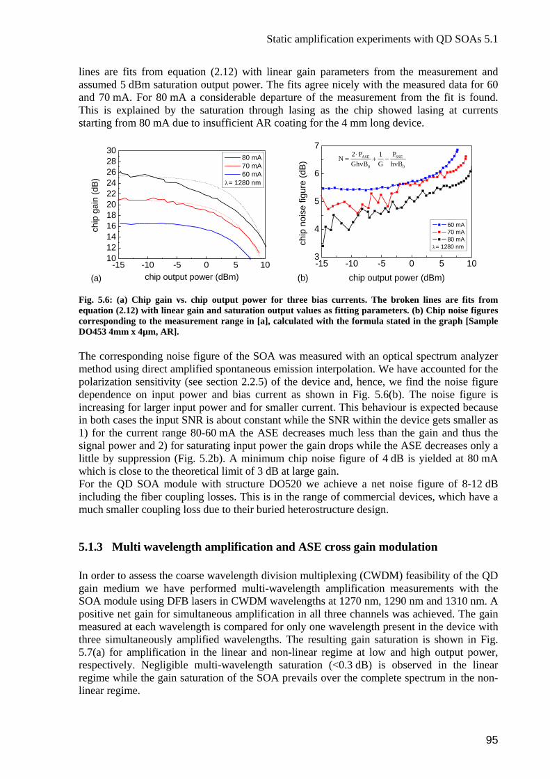
Static amplification experiments with QD SOAs 5.1
lines are fits from equation (2.12) with linear gain parameters from the measurement and assumed 5 dBm saturation output power. The fits agree nicely with the measured data for 60 and 70 mA. For 80 mA a considerable departure of the measurement from the fit is found. This is explained by the saturation through lasing as the chip showed lasing at currents starting from 80 mA due to insufficient AR coating for the 4 mm long device.
-15 -10 -5 0 5 101012141618202224262830
80 mA 70 mA 60 mA
λ= 1280 nm
chip
gai
n (d
B)
chip output power (dBm)(a)
-15 -10 -5 0 5 103
4
5
6
7 ASE SSE
0 0
2 P P1NGh B G h B
⋅= + −
ν ν
60 mA 70 mA 80 mA
λ= 1280 nm
ise
figur
e (d
B)
easured with an optical spectrum analyzer method using direct amplified spontaneous emission interpolation. We have accounted for the polarization sensitivity (see section 2.2.5) of the device and, hence, we find the noise figure dependence on input power and bias current as shown in Fig. 5.6(b). The noise figure is increasing for larger input power and for smaller current. This behaviour is expected because in both cases the input SNR is about constant while the SNR within the device gets smaller as 1) for the current range 80-60 mA the ASE decreases much less than the gain and thus the signal power and 2) for saturating input power the gain drops while the ASE decreases only a little by suppression (Fig. 5.2b). A minimum chip noise figure of 4 dB is yielded at 80 mA which is close to the theoretical limit of 3 dB at large gain. For the QD SOA module with structure DO520 we achieve a net noise figure of 8-12 dB including the fiber coupling losses. This is in the range of commercial devices, which have a much smaller coupling loss due to their buried heterostructure design.
ultiplexing (CWDM) feasibility of the QD
chip
no
chip output power (dBm)(b)
Fig. 5.6: (a) Chip gain vs. chip output power for three bias currents. The broken lines are fits from equation (2.12) with linear gain and saturation output values as fitting parameters. (b) Chip noise figures corresponding to the measurement range in [a], calculated with the formula stated in the graph [Sample DO453 4mm x 4µm, AR]. The corresponding noise figure of the SOA was m
5.1.3 Multi wavelength amplification and ASE cross gain modulation
order to assess the coarse wavelength division mIngain medium we have performed multi-wavelength amplification measurements with the SOA module using DFB lasers in CWDM wavelengths at 1270 nm, 1290 nm and 1310 nm. A positive net gain for simultaneous amplification in all three channels was achieved. The gain measured at each wavelength is compared for only one wavelength present in the device with three simultaneously amplified wavelengths. The resulting gain saturation is shown in Fig. 5.7(a) for amplification in the linear and non-linear regime at low and high output power, respectively. Negligible multi-wavelength saturation (<0.3 dB) is observed in the linear regime while the gain saturation of the SOA prevails over the complete spectrum in the non-linear regime.
95

5 Application Oriented Experiments with QD SOAs
1260 1270 1280 1290 1300 1310 1320
0
1
2
-60-50-40-30-20-10
gain
sat
urat
ion
(dB
)
wavelength (nm)
switching from 1 λ to 3 λ non-linear regime linear regime < 5 dBm
output input
inte
nsity
(dB
m)
(a)1260 1270 1280 1290 1300 1310 1320
-2
0
2
4
6
8
10
ECL (Pin= -3 dBm, DFB off) ECL (DFB on)
DFB (Pin= -5 dBm, ECL off) DFB (ECL on)
net g
ain
(dB
)
ECL wavelength (nm)
λDFB= 1291.3 nm
(b) Fig. 5.7: (a) Bottom: Spectra of three CWDM DFB lasers before and after amplification at 1270, 1290 and 1310 nm. Top: Gain saturation, i.e. difference of gain for amplification of one or three wavelengths simultaneously, for linear and non-linear gain regime. (b) The cross-gain saturation is mapped between
FB laser at fixed wavelength 1291 nm and ECL scanned from 1260 to 1320 nm in the non-linear regimeD
e close to each other. This is attributed to
of the SOA. This is also found when an external cavity laser is tuned from 1260 to 1320 nm with respect to a fixed DFB-laser wavelength to find the influence of the distance of two signals present in the amplifier. We observe no suppression of the gain if both signals operate in the linear regime, i.e. the both wavelengths are amplified independently no matter how close they are. The situation changes if the input signals saturate the amplifier. Fig. 5.7(b) presents the case where the power of both wavelengths independently leads to a gain saturation of the device. If both signals are amplified, the gain of each of the two wavelengths is suppressed further and this suppression is found to be present over the whole spectral bandwidth of the SOA with a
aximum as large as 2 dB when the wavelengths armcarrier depletion of the shared carrier reservoir. In the linear regime of the SOA at low input power no influence of the CWDM wavelengths is found, which shows the potential for pattern effect free multi-wavelength data transmission.
1150 1200 1250 1300 1350-60
1450 1500 1550-14
-6-4-20
150 mA 120 mA 80 mA 50 mA-40
-35
ce (d
B)
Bm)
-55
-50
-45
ASE
(d
-12-10-8
Psatin
10Pin
wavelength (nm)
calculation by A. Bilenca
(b)
sat
ASE
diff
eren
alpha = 1.5
(a) wavelength (nm)
Fig. 5.8: (a) ASE spectra of module at various bias currents. (b) Calculation of ASE difference for strongly saturating signal for a quantum dash amplifier. [Adapted from modeling of A. Bilenca [112]. Courtesy of G. Eisenstein.] The cross gain modulation can be assessed by measurement of the ASE suppression due to a saturating input signal. As a motivation the theoretical investigation on noise properties of quantum dot SOAs at 1.55 µm is considered [112]. The ASE of an optical amplifier is related to the carrier distribution in energy, the gain spectrum, and the saturation properties which in turn are strongly affected by the gain inhomogeneity and the gain dynamics. The noise is
96
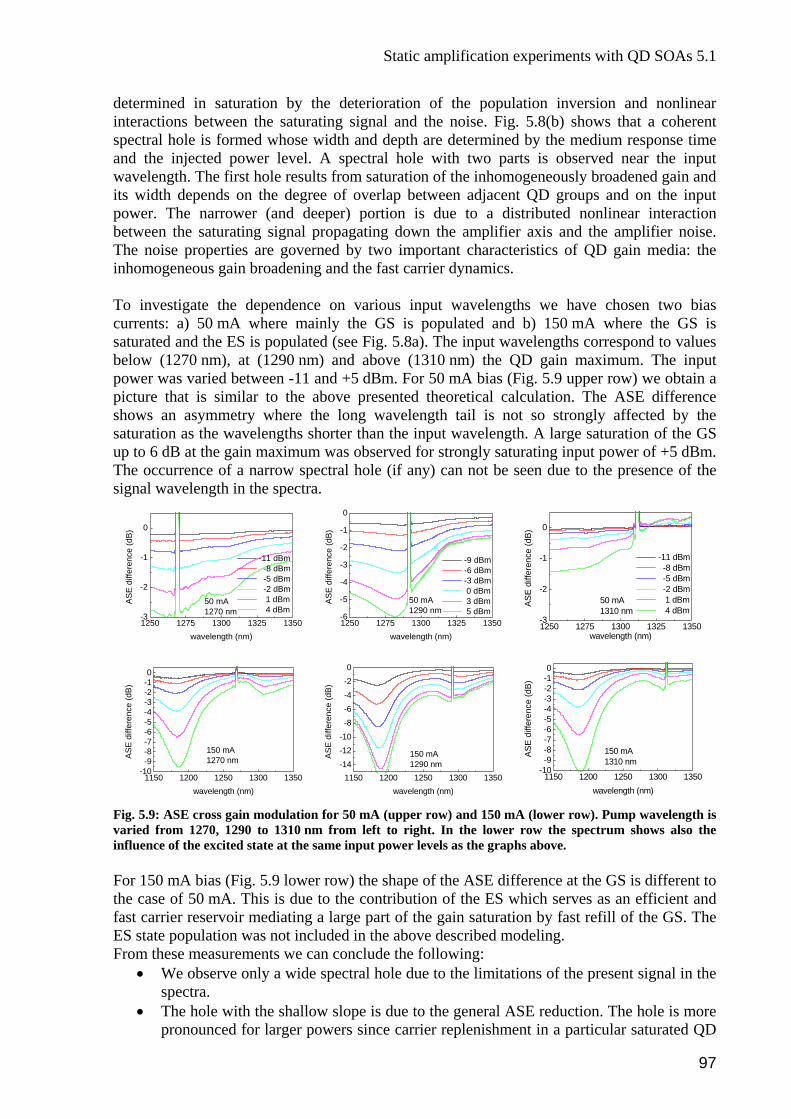
Static amplification experiments with QD SOAs 5.1
determined in saturation by the deterioration of the population inversion and nonlinear interactions between the saturating signal and the noise. Fig. 5.8(b) shows that a coherent spectral hole is formed whose width and depth are determined by the medium response time and the injected power level. A spectral hole with two parts is observed near the input wavelength. The first hole results from saturation of the inhomogeneously broadened gain and its width depends on the degree of overlap between adjacent QD groups and on the input power. The narrower (and deeper) portion is due to a distributed nonlinear interaction between the saturating signal propagating down the amplifier axis and the amplifier noise. The noise properties are governed by two important characteristics of QD gain media: the inhomogeneous gain broadening and the fast carrier dynamics. To investigate the dependence on various input wavelengths we have chosen two bias currents: a) 50 mA where mainly the GS is populated and b) 150 mA where the GS is saturated and the ES is populated (see Fig. 5.8a). The input wavelengths correspond to values below (1270 nm), at (1290 nm) and above (1310 nm) the QD gain maximum. The input power was varied between -11 and +5 dBm. For 50 mA bias (Fig. 5.9 upper row) we obtain a picture that is similar to the above presented theoretical calculation. The ASE difference shows an asymmetry where the long wavelength tail is not so strongly affected by the
e spectra.
saturation as the wavelengths shorter than the input wavelength. A large saturation of the GS up to 6 dB at the gain maximum was observed for strongly saturating input power of +5 dBm. The occurrence of a narrow spectral hole (if any) can not be seen due to the presence of the
gnal wavelength in thsi
1250 1275 1300 1325 1350-3
-2
-1
0
-11 dBm -8 dBm -5 dBm -2 dBm 1 dBm 4 dBm
50 mA1270 nm
AS
E d
iffer
ence
(dB
)
wavelength (nm)1250 1275 1300 1325 1350-6
-5
-4
-3
-2
-1
0
-9 dBm -6 dBm -3 dBm 0 dBm 3 dBm 5 dBm
AS
E d
iffer
ence
(dB
)
wavelength (nm)
50 mA1290 nm
1250 1275 1300 1325 1350-3
-2
-1
0
-11 dBm -8 dBm -5 dBm -2 dBm 1 dBm 4 dBm
ASE
diff
eren
ce (d
B)
wavelength (nm)
50 mA1310 nm
1150 1200 1250 1300 1350-10-9-8-7-6-5-4-3-2-10
ffere
nce
(dB
)A
SE
di
150 mA1270 nm
wavelength (nm)1150 1200 1250 1300 1350
-14-12-10-8-6-4-20
iffer
ence
(dB
)A
SE
d
150 mA1290 nm
wavelength (nm)
1150 1200 1250 1300 1350-10-9-8
-10
-7-6-5-4-3-2
diff
eren
ce (d
B)AS
E
nm)
150 mA1310 nm
• The hole with the shallow slope is due to the general ASE reduction. The hole is more
pronounced for larger powers since carrier replenishment in a particular saturated QD
wavelength (
Fig. 5.9: ASE cross gain modulation for 50 mA (upper row) and 150 mA (lower row). Pump wavelength is varied from 1270, 1290 to 1310 nm from left to right. In the lower row the spectrum shows also the influence of the excited state at the same input power levels as the graphs above. For 150 mA bias (Fig. 5.9 lower row) the shape of the ASE difference at the GS is different to the case of 50 mA. This is due to the contribution of the ES which serves as an efficient and fast carrier reservoir mediating a large part of the gain saturation by fast refill of the GS. The ES state population was not included in the above described modeling. From these measurements we can conclude the following:
• We observe only a wide spectral hole due to the limitations of the present signal in the spectra.
97
5 Application Oriented Experiments with QD SOAs
group originates from other, spectrally neighboring, QD groups which is typical for an inhomogeneously broadened gain medium.
• For short wavelengths, the spectral hole is smaller due to the reduced four wave mixing efficiency and the strong coupling to the ES and wetting layer. For long wavelengths, the spectral hole is also smaller than the one at the gain peak because of the larger saturation power.
5.1.4 Polarization dependence of QD SOAs The polarization sensitivity of SOAs must be examined in order to improve the performance
ents in optical systems. From a technical point of view a gain difference between
s two possible polarizations. In the case of the transverse-magnetic (TM)-mode e polarization is aligned with the z-direction. For the transverse-electric (TE)-mode the
fibers remain untouched.
(a)
of these elemth . e optical TE- and TM-mode of less than 3 dB (1 dB) is desired in data transmission systems In literature different terms are used in the framework of polarization of amplifiers and gain media. We adhere to the definition given in chapter 2.3.2. Light which propagates along the xy-plane hathpolarization is along the xy-plane, here we assume it to be parallel to the x-direction. Therefore, the TE- and TM-modes are often referred to as parallel and vertical mode, respectively. The difference between parallel and vertical vector of the polarization specifies the so-called polarization ratio. In a calibration routine the electrical controllable polarization controller (HP11896A) is scanned until maximum output of TE or TM (set by polarization filter after the taper) is detected (Fig. 5.10a). The positions of four fiber loops inside the polarization controller are recorded. Although all fibers are non-polarization-maintaining SMF the polarization output of the taper is stable and reproducible as long as the
(b) Fig. 5.10: Schematic setup to measure TE/TM polarization dependence of the QD SOA chip. (a) Calibration routine to set the output polarization of the fiber taper. The polarization controller (PC) is controllable via GPIB. (b) Measurement of the polarization dependent gain of the chip under test by setting the input polarization with the PC.
rolled by the divided output signal. The gain is calculated from the optical
By setting the positions of the polarization controller the input signal into the QD SOA is adjusted to TE or TM when the gain is measured. The alignment of the input and output fiber apers is contt
spectrum as described in section 4.2.2.
98
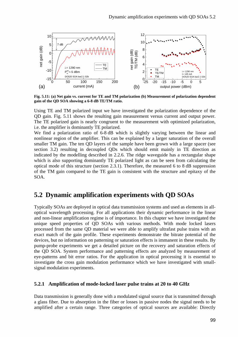
Dynamic amplification experiments with QD SOAs 5.2
0 50 100 150 200-15
-10
-5
0
5
10
TE TM
net g
ain
(dB
)
λ= 1290 nmPtpr
in =-5 dBmDO520 SOA bar2.1 02b
current (mA)
7 dB
-25 -200
2
4
6
8
10
12
-15 -10 -5 0 5
λ= 1290 nmI= 145 mADO520 SOA bar2.1 02b
net g
ain
(dB
)TE
/TM
(dB
)
output power (dBm)
TE
TM
(b)
TE/TM
(a)
Fig. 5.11: (a) Net gain vs. current for TE and TM polarization (b) Measurement of polarization dependent gain of the QD SOA showing a 6-8 dB TE/TM ratio. Using TE and TM polarized input we have investigated the polarization dependence of the QD gain. Fig. 5.11 shows the resulting gain measurement versus current and output power. The TE polarized gain is nearly congruent to the measurement with optimized polarization, i.e. the amplifier is dominantly TE polarized. We find a polarization ratio of 6-8 dB which is slightly varying between the linear and nonlinear region of the amplifier. This can be explained by a larger saturation of the overall smaller TM gain. The ten QD layers of the sample have been grown with a large spacer (see section 3.2) resulting in decoupled QDs which should emit mainly in TE direction as indicated by the modelling described in 2.2.6. The ridge waveguide has a rectangular shape which is also supporting dominantly TE polarized light as can be seen from calculating the optical mode of this structure (section 2.3.1). Therefore, the measured 6 to 8 dB suppression of the TM gain compared to the TE gain is consistent with the structure and epitaxy of the SOA. 5.2 Dynamic amplification experiments with QD SOAs Typically SOAs are deployed in optical data transmission systems and used as elements in all- optical wavelength processing. For all applications their dynamic performance in the linear and non-linear amplification regime is of importance. In this chapter we have investigated the unique speed properties of QD SOAs with various methods. With mode locked lasers processed from the same QD material we were able to amplify ultrafast pulse trains with an exact match of the gain profile. These experiments demonstrate the bitrate potential of the devices, but no information on patterning or saturation effects is immanent in these results. B
sing it is essential to
0 GHz
Dat ra g samp i
y pump-probe experiments we get a detailed picture on the recovery and saturation effects of the QD SOA. System performance and patterning effects are analyzed by measurement of ye-patterns and bit error ratios. For the application in optical procese
investigate the cross gain modulation performance which we have investigated with small-signal modulation experiments.
5.2.1 Amplification of mode-locked laser pulse trains at 20 to 4
a t ansmission is generally done with a modulated signal source that is transmitted through las fiber. Due to absorption in the fiber or losses in passive nodes the signal needs to be lif ed after a certain range. Three categories of optical sources are available: Directly
99
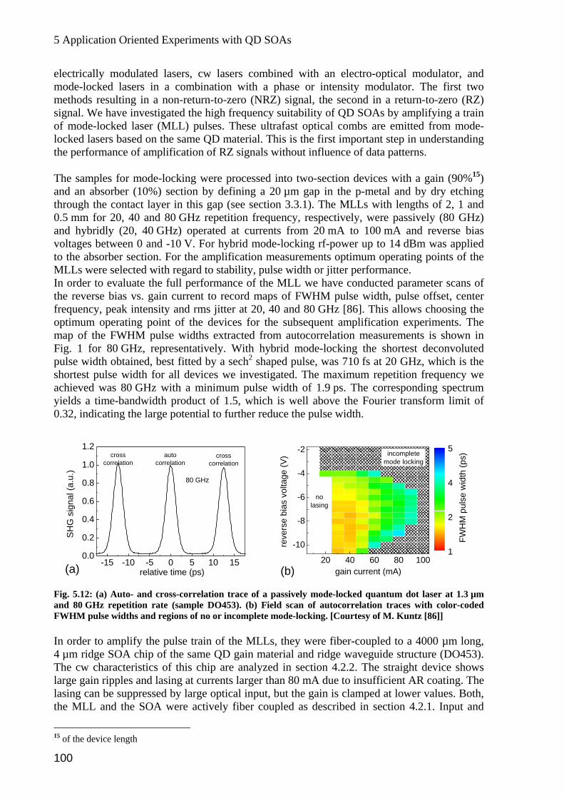
5 Application Oriented Experiments with QD SOAs
electricmode-l e or intensity modulator. The first two me dsignal. of modlocked material. This is the first important step in understanding
e performance of amplification of RZ signals without influence of data patterns.
two-section devices with a gain (90%15) nd an absorber (10%) section by defining a 20 µm gap in the p-metal and by dry etching
oltages between 0 and -10 V. For hybrid mode-locking rf-power up to 14 dBm was applied
ively. With hybrid mode-locking the shortest deconvoluted ulse width obtained, best fitted by a sech2 shaped pulse, was 710 fs at 20 GHz, which is the
ally modulated lasers, cw lasers combined with an electro-optical modulator, and ocked lasers in a combination with a phas
tho s resulting in a non-return-to-zero (NRZ) signal, the second in a return-to-zero (RZ) We have investigated the high frequency suitability of QD SOAs by amplifying a train e-locked laser (MLL) pulses. These ultrafast optical combs are emitted from mode-lasers based on the same QD
th
The samples for mode-locking were processed into athrough the contact layer in this gap (see section 3.3.1). The MLLs with lengths of 2, 1 and 0.5 mm for 20, 40 and 80 GHz repetition frequency, respectively, were passively (80 GHz) and hybridly (20, 40 GHz) operated at currents from 20 mA to 100 mA and reverse bias vto the absorber section. For the amplification measurements optimum operating points of the MLLs were selected with regard to stability, pulse width or jitter performance. In order to evaluate the full performance of the MLL we have conducted parameter scans of the reverse bias vs. gain current to record maps of FWHM pulse width, pulse offset, center frequency, peak intensity and rms jitter at 20, 40 and 80 GHz [86]. This allows choosing the optimum operating point of the devices for the subsequent amplification experiments. The map of the FWHM pulse widths extracted from autocorrelation measurements is shown in Fig. 1 for 80 GHz, representatpshortest pulse width for all devices we investigated. The maximum repetition frequency we achieved was 80 GHz with a minimum pulse width of 1.9 ps. The corresponding spectrum yields a time-bandwidth product of 1.5, which is well above the Fourier transform limit of 0.32, indicating the large potential to further reduce the pulse width.
-15 -10 -5 0 5 10 150.0
0.2
0.4
0.6
0.8
1.0
1.2
SH
G s
igna
l (
20 40 60 80 100
-10
-8
-6
-4
-2 incompletemode locking
nolasing
FWH
M p
ulse
wid
th (p
s)
80 GHz
crosscorrelation
autocorrelation
crosscorrelation
reve
rse
bias
vol
t(V
)ag
e
a.u.
)
relative time (ps)(a) gain current (mA)
1
2
4
5
3). (b) Field scan of autocorrelation traces with color-coded WHM pulse widths and regions of no or incomplete mode-locking. [Courtesy of M. Kuntz [86]]
rge gain ripples and lasing at currents larger than 80 mA due to insufficient AR coating. The lasing can be suppressed by large optical input, but the gain is clamped at lower values. Both, the MLL and the SOA were actively fiber coupled as described in section 4.2.1. Input and
(b)
Fig. 5.12: (a) Auto- and cross-correlation trace of a passively mode-locked quantum dot laser at 1.3 µm and 80 GHz repetition rate (sample DO45F In order to amplify the pulse train of the MLLs, they were fiber-coupled to a 4000 µm long, 4 µm ridge SOA chip of the same QD gain material and ridge waveguide structure (DO453). The cw characteristics of this chip are analyzed in section 4.2.2. The straight device shows la
15 of the device length
100
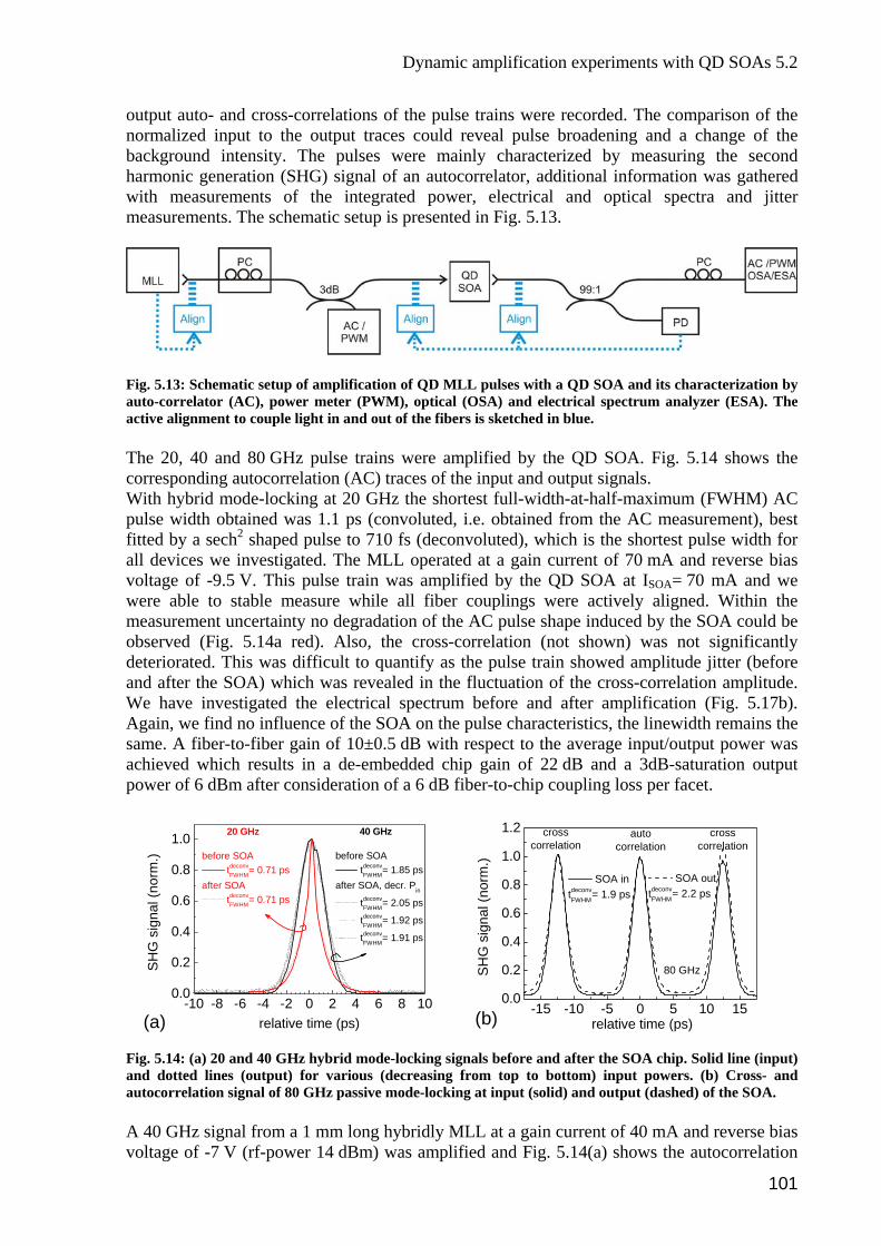
Dynamic amplification experiments with QD SOAs 5.2
output auto- and cross-correlations of the pulse trains were recorded. The comparison of the normalized input to the output traces could reveal pulse broadening and a change of the background intensity. The pulses were mainly characterized by measuring the second harmonic generation (SHG) signal of an autocorrelator, additional information was gathered with measurements of the integrated power, electrical and optical spectra and jitter measurements. The schematic setup is presented in Fig. 5.13.
ig. 5.13: Schematic setup of amplification of QD MLF L pulses with a QD SOA and its characterization by
rated. This was difficult to quantify as the pulse train showed amplitude jitter (before nd after the SOA) which was revealed in the fluctuation of the cross-correlation amplitude.
mains the
me. A fiber-to-fiber gain of 10±0.5 dB with respect to the average input/output power was
auto-correlator (AC), power meter (PWM), optical (OSA) and electrical spectrum analyzer (ESA). The active alignment to couple light in and out of the fibers is sketched in blue. The 20, 40 and 80 GHz pulse trains were amplified by the QD SOA. Fig. 5.14 shows the corresponding autocorrelation (AC) traces of the input and output signals. With hybrid mode-locking at 20 GHz the shortest full-width-at-half-maximum (FWHM) AC pulse width obtained was 1.1 ps (convoluted, i.e. obtained from the AC measurement), best fitted by a sech2 shaped pulse to 710 fs (deconvoluted), which is the shortest pulse width for all devices we investigated. The MLL operated at a gain current of 70 mA and reverse bias voltage of -9.5 V. This pulse train was amplified by the QD SOA at ISOA= 70 mA and we were able to stable measure while all fiber couplings were actively aligned. Within the measurement uncertainty no degradation of the AC pulse shape induced by the SOA could be observed (Fig. 5.14a red). Also, the cross-correlation (not shown) was not significantly deterioaWe have investigated the electrical spectrum before and after amplification (Fig. 5.17b).Again, we find no influence of the SOA on the pulse characteristics, the linewidth resaachieved which results in a de-embedded chip gain of 22 dB and a 3dB-saturation output power of 6 dBm after consideration of a 6 dB fiber-to-chip coupling loss per facet.
-10 -8 -6 -4 -2 0 2 4 6 80.0
0.2
0.4
0.6
0.8
1.0
10(a)
SH
G s
igna
l (no
rm.)
40 GHz
before SOA
relative time (ps)
tdeconvFWHM= 1.85 ps
after SOA, decr. Pin
tdeconvFWHM= 2.05 ps
tdeconvFWHM= 1.92 ps
tdeconvFWHM= 1.91 ps
20 GHz
before SOA tdeconv
FWHM= 0.71 psafter SOA
tdeconvFWHM= 0.71 ps
-15 -10 -5 0 5 10 150.0
0.2
0.4
0.6
0.8
1.0
1.2
SOA intdeconvFWHM= 1.9 ps
SH
G s
igna
l (no
rm.)
relative time (ps)
SOA outtdeconvFWHM= 2.2 ps
80 GHz
crosscorrelation
autocorrelation
crosscorrelation
(b)
nd dotted lines (output) for various (decreasing from top to bottom) input powers. (b) Cross- and
voltage of -7 V (rf-power 14 dBm) was amplified and Fig. 5.14(a) shows the autocorrelation
Fig. 5.14: (a) 20 and 40 GHz hybrid mode-locking signals before and after the SOA chip. Solid line (input) aautocorrelation signal of 80 GHz passive mode-locking at input (solid) and output (dashed) of the SOA. A 40 GHz signal from a 1 mm long hybridly MLL at a gain current of 40 mA and reverse bias
101
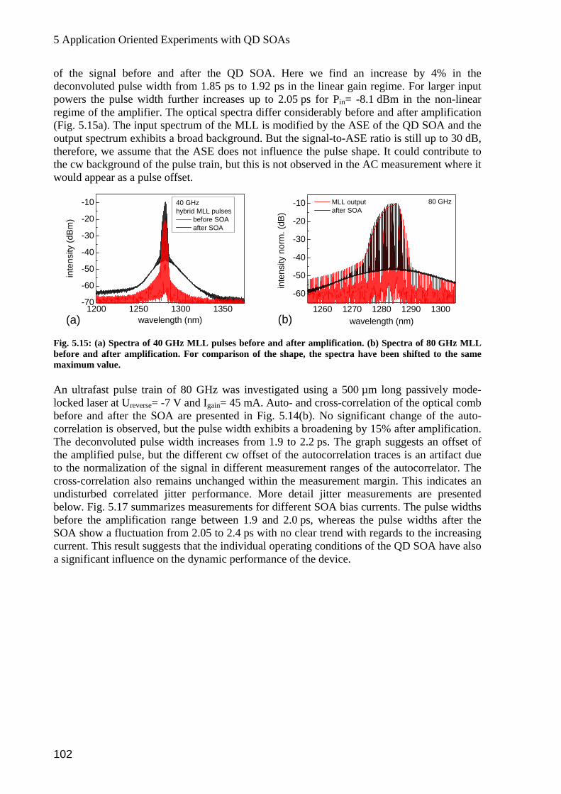
5 Application Oriented Experiments with QD SOAs
of the signal before and after the QD SOA. Here we find an increase by 4% in the deconvoluted pulse width from 1.85 ps to 1.92 ps in the linear gain regime. For larger input powers the pulse width further increases up to 2.05 ps for Pin= -8.1 dBm in the non-linear regime of the amplifier. The optical spectra differ considerably before and after amplification (Fig. 5.15a). The input spectrum of the MLL is modified by the ASE of the QD SOA and the output spectrum exhibits a broad background. But the signal-to-ASE ratio is still up to 30 dB, therefore, we assume that the ASE does not influence the pulse shape. It could contribute to
e cw background of the pulse train, but this is not observed in the AC measurement where it thwould appear as a pulse offset.
-50
-40
-30
-20
-10
1200 1250 1300 1350-70
-60
inte
nsity
(dB
m)
wavelength (nm)
40 GHzhybrid MLL pulses
before SOA after SOA
-40
-30
-20
-10
(a)1260 1270 1280 1290 1300
-60
-50
MLL output after SOA
nsity
nor
m. (
dB)
80 GHz
inte
wavelength (nm)(b)
Fig. 5.15: (a) Spectra of 40 GHz MLL pulses before and after amplification. (b) Spectra of 80 GHz MLL before and after amplification. For comparison of the shape, the spectra have been shifted to the same maximum value. An ultrafast pulse train of 80 GHz was investigated using a 500 µm long passively mode-locked laser at Ureverse= -7 V and Igain= 45 mA. Auto- and cross-correlation of the optical comb before and after the SOA are presented in Fig. 5.14(b). No significant change of the auto-correlation is observed, but the pulse width exhibits a broadening by 15% after amplification. The deconvoluted pulse width increases from 1.9 to 2.2 ps. The graph suggests an offset of the amplified pulse, but the different cw offset of the autocorrelation traces is an artifact due to the normalization of the signal in different measurement ranges of the autocorrelator. The cross-correlation also remains unchanged within the measurement margin. This indicates an undisturbed correlated jitter performance. More detail jitter measurements are presented below. Fig. 5.17 summarizes measurements for different SOA bias currents. The pulse widths before the amplification range between 1.9 and 2.0 ps, whereas the pulse widths after the SOA show a fluctuation from 2.05 to 2.4 ps with no clear trend with regards to the increasing current. This result suggests that the individual operating conditions of the QD SOA have also a significant influence on the dynamic performance of the device.
102
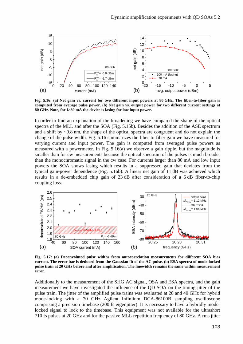
Dynamic amplification experiments with QD SOAs 5.2
0 20 40 60 80 100 120 140-15
-10
-5
0
5
10
15
gai
n (d
B)
8101214
-20 -15 -10 -5 0 50246
ne
avg. output power (dBm)
t gai
n (d
B)
net
current (mA)
Pavgin = -5.0 dBm
Pavgin = -1.7 dBm
80 GHz
(a)
100 mA (lasing) 70 mA
80 GHz
(b)
ig. 5.16: (a) Net gain vs. current for two different input powers at 80 GHz. The fiber-to-fiber gain is
order to find an explanation of the broadening we have compared the shape of the optical
do not explain the
100 120 140 1601.81.92.02.1
Fcomputed from average pulse power. (b) Net gain vs. output power for two different current settings at 80 GHz. Note, for I>80 mA the device is lasing for low input power. Inspectra of the MLL and after the SOA (Fig. 5.15b). Besides the addition of the ASE spectrum and a shift by ~0.8 nm, the shape of the optical spectra are congruent and change of the pulse width. Fig. 5.16 summarizes the fiber-to-fiber gain we have measured for varying current and input power. The gain is computed from averaged pulse powers as measured with a powermeter. In Fig. 5.16(a) we observe a gain ripple, but the magnitude is smaller than for cw measurements because the optical spectrum of the pulses is much broader than the monochromatic signal in the cw case. For currents larger than 80 mA and low input powers the SOA shows lasing which results in a suppressed gain that deviates from the typical gain-power dependence (Fig. 5.16b). A linear net gain of 11 dB was achieved which results in a de-embedded chip gain of 23 dB after consideration of a 6 dB fiber-to-chip coupling loss.
2.22.32.42.52.6
40 60 80
-50
-40
-30
ed F
WH
M (p
s)de
conv
olut
urrent (mA)
Pin= -5 dBm
20.25 20.28 20.31-80
-70
-60
ES
frequency (GHz)
A in
tens
ity (d
Bm)
before SOA∆fFWHM= 1.12 MHz
after SOA∆fFWHM= 1.06 MHz
20 GHz
decon. FWHM of MLL
80 GHz
(a) SOA c (b)
Fig. 5.17: (a) Deconvoluted pulse widths from autocorrelation measurements for different SOA bias current. The error bar is deduced from the Gaussian fit of the AC pulse. (b) ESA spectra of mode-locked pulse train at 20 GHz before and after amplification. The linewidth remains the same within measurement error. Additionally to the measurement of the SHG AC signal, OSA and ESA spectra, and the gain measurement we have investigated the influence of the QD SOA on the timing jitter of the
e-
pulse train. The jitter of the amplified pulse trains was evaluated at 20 and 40 GHz for hybrid mode-locking with a 70 GHz Agilent Infiniium DCA-86100B sampling oscilloscope omprising a precision timebase (200 fs eigenjitter). It is necessary to have a hybridly modc
locked signal to lock to the timebase. This equipment was not available for the ultrashort 710 fs pulses at 20 GHz and for the passive MLL repetition frequency of 80 GHz. A rms jitter
103
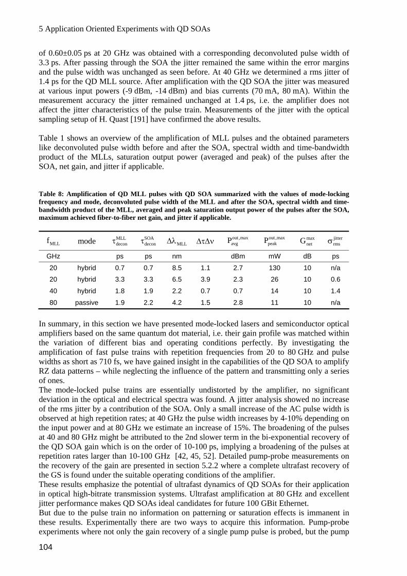
5 Application Oriented Experiments with QD SOAs
of 0.60±0.05 ps at 20 GHz was obtained with a corresponding deconvoluted pulse width of 3.3 ps. After passing through the SOA the jitter remained the same within the error margins and the pulse width was unchanged as seen before. At 40 GHz we determined a rms jitter of 1.4 ps for the QD MLL source. After amplification with the QD SOA the jitter was measured at various input powers (-9 dBm, -14 dBm) and bias currents (70 mA, 80 mA). Within the measurement accuracy the jitter remained unchanged at 1.4 ps, i.e. the amplifier does not affect the jitter characteristics of the pulse train. Measurements of the jitter with the optical sampling setup of H. Quast [191] have confirmed the above results. Table 1 shows an overview of the amplification of MLL pulses and the obtained parameters like deconvoluted pulse width before and after the SOA, spectral width and time-bandwidth product of the MLLs, saturation output power (averaged and peak) of the pulses after the SOA, net gain, and jitter if applicable. Table 8: Amplification of QD MLL pulses with QD SOA summarized with the values of mode-locking frequency and mode, deconvoluted pulse width of the MLL and after the SOA, spectral width and time-bandwidth product of the MLL, averaged and peak saturation output power of the pulses after the SOA, maximum achieved fiber-to-fiber net gain, and jitter if applicable.
MLL MLLf mode MLLdeconτ SOA
deconτ ∆λ ∆τ∆ν out,maxavgP out,max
peakP maxnetG jitter
rmsσ
GHz ps ps nm dBm mW dB ps
20 hybrid 0.7 0.7 8.5 1.1 2.7 130 10 n/a
20 hybrid 3.3 3.3 6.5 3.9 2.3 26 10 0.6
40 hybrid 1.8 1.9 2.2 0.7 0.7 14 10 1.4
80 passive 1.9 2.2 4.2 1.5 2.8 11 10 n/a
In summary, in this section we have presented mode-locked lasers and semiconductor optical amplifiers based on the same quantum dot material, i.e. their gain profile was matched within the variation of different bias and operating conditions perfectly. By investigating the amplification of fast pulse trains with repetition frequencies from 20 to 80 GHz and pulse widths as short as 710 fs, we have gained insight in the capabilities of the QD SOA to amplify RZ data patterns – while neglecting the influence of the pattern and transmitting only a series of ones. The mode-locked pulse trains are essentially undistorted by the amplifier, no significant deviation in the optical and electrical spectra was found. A jitter analysis showed no increase of the rms jitter by a contribution of the SOA. Only a small increase of the AC pulse width is observed at high repetition rates; at 40 GHz the pulse width increases by 4-10% depending on the input power and at 80 GHz we estimate an increase of 15%. The broadening of the pulses at 40 and 80 GHz might be attributed to the 2nd slower term in the bi-exponential recovery of the QD SOA gain which is on the order of 10-100 ps, implying a broadening of the pulses at repetition rates larger than 10-100 GHz [42, 45, 52]. Detailed pump-probe measurements on the recovery of the gain are presented in section 5.2.2 where a complete ultrafast recovery of the GS is found under the suitable operating conditions of the amplifier. These results emphasize the potential of ultrafast dynamics of QD SOAs for their application in optical high-bitrate transmission systems. Ultrafast amplification at 80 GHz and excellent jitter performance makes QD SOAs ideal candidates for future 100 GBit Ethernet. But due to the pulse train no information on patterning or saturation effects is immanent in these results. Experimentally there are two ways to acquire this information. Pump-probe experiments where not only the gain recovery of a single pump pulse is probed, but the pump
104
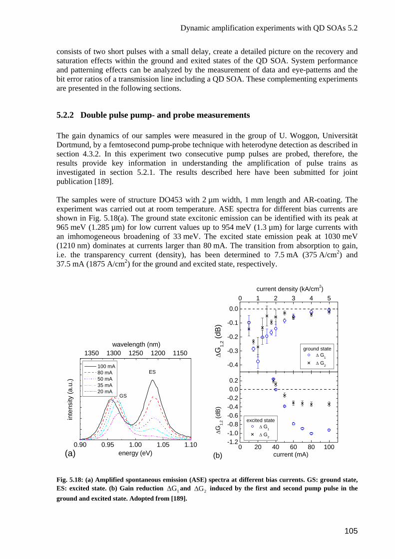
Dynamic amplification experiments with QD SOAs 5.2
consists of two short pulses with a small delay, create a detailed picture on the recovery and saturation effects within the ground and exited states of the QD SOA. System performance and patterning effects can be analyzed by the measurement of data and eye-patterns and the bit error ratios of a transmission line including a QD SOA. These complementing experiments are presented in the following sections.
5.2.2 Double pulse pump- and probe measurements The gain dynamics of our samples were measured in the group of U. Woggon, Universität Dortmund, by a femtosecond pump-probe technique with heterodyne detection as described in section 4.3.2. In this experiment two consecutive pump pulses are probed, therefore, the results provide key information in understanding the amplification of pulse trains as investigated in section 5.2.1. The results described here have been submitted for joint ublication [189]. p
The samples were of structure DO453 with 2 µm width, 1 mm length and AR-coating. The experiment was carried out at room temperature. ASE spectra for different bias currents are shown in Fig. 5.18(a). The ground state excitonic emission can be identified with its peak at 965 meV (1.285 µm) for low current values up to 954 meV (1.3 µm) for large currents with an imhomogeneous broadening of 33 meV. The excited state emission peak at 1030 meV (1210 nm) dominates at currents larger than 80 mA. The transition from absorption to gain, i.e. the transparency current (density), has been determined to 7.5 mA (375 A/cm2) and 37.5 mA (1875 A/cm2) for the ground and excited state, respectively.
0 20 40 60 80 100-1.2
current density (kA/cm2)
0.90 0.95 1.00 1.05 1.10
1350 1300 1250 1200 1150
GS
inte
nsity
(a.u
.)
energy (eV)
100 mA 80 mA 50 mA 35 mA 20 mA
wavelength (nm)
ES
(a)
-1.0-0.8-0.6-0.4-0.20.00.2
-0.4
-0.3
-0.2
-0.1
0.00 1 2 3 4 5
ground state ∆ G1
∆ G2
∆G
1,2 (d
B)
excited state ∆ G1
∆ G2
∆G1,
2 (dB
)
current (mA)(b)
Fig. 5.18: (a) Amplified spontaneous emission (ASE) spectra at different bias currents. GS: ground state, ES: excited state. (b) Gain reduction 1G∆ and 2G∆ induced by the first and second pump pulse in the ground and excited state. Adopted from [189].
105
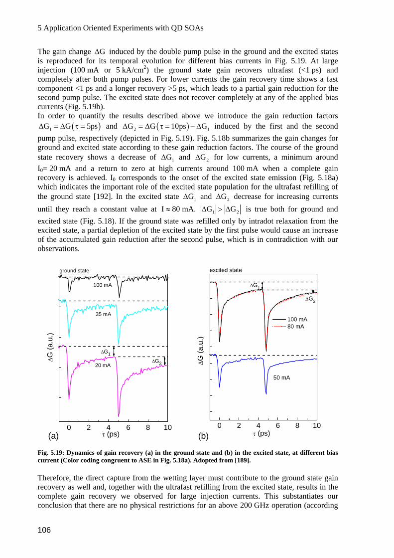
5 Application Oriented Experiments with QD SOAs
The gain change G∆ induced by the double pump pulse in the ground and the excited states is reproduced for its temporal evolution for different bias currents in Fig. 5.19. At large injection (100 mA or 5 kA/cm2) the ground state gain recovers ultrafast (<1 ps) and completely after both pump pulses. For lower currents the gain recovery time shows a fast component <1 ps and a longer recovery >5 ps, which leads to a partial gain reduction for the second pump pulse. The excited state does not recover completely at any of the applied bias currents (Fig. 5.19b). In order to quantify the results described above we introduce the gain reduction factors
G G 5ps∆ τ = and G G 10ps G∆ = ∆ τ = − ∆ induced by the first and the second ( )1 2 1
pump pulse, respectively (depicted in Fig. 5.19). Fig. 5.18b summarizes the gain changes for ground and excited state according to these gain reduction factors. The course of the ground state recovery shows a decrease of G∆ and G
( )
1 2
∆ =
∆ for low currents, a minimum around = 20 mA and a return to zero at high currents around 100 mA when a complete gain covery is achieved. I0 corresponds to the onset of the excited state emission (Fig. 5.18a)
I0rewhich indicates the important role of the excited state population for the ultrafast refilling of the ground state [192]. In the excited state 1G∆ and 2G∆ decrease for increasing currents until they reach a constant value at I ≈ 80 mA. 1G G∆ > ∆ is true both for ground and 2
xcited state (Fig. 5.18). If the ground state was refilled only by intradot relaxation from the excited state, a partial depletion of the excited state by the first pulse would cause an increas of the accumulated gain reduction after the second pulse, which is in contradiction with our observations.
ee
0 2 4 6 8 10(a)
∆G2
∆G1
20 mA
35 mA
100 mA
groun
d state
∆G (a
.u.)
τ (ps)0 2 4 6 8 10
∆G2
∆G1
excite ed stat
100 mA 80 mA
∆G (a
.u.)
50 mA
τ (ps)(b)
Fig. 5.19: Dynamics of gain recovery (a) in the ground state and (b) in the excited state, at different bias current (Color coding congruent to ASE in Fig. 5.18a). Adopted from [189]. Therefore, the direct capture from the wetting layer must contribute to the ground state gain recovery as well and, together with the ultrafast refilling from the excited state, results in the complete gain recovery we observed for large injection currents. This substantiates our conclusion that there are no physical restrictions for an above 200 GHz operation (according
106
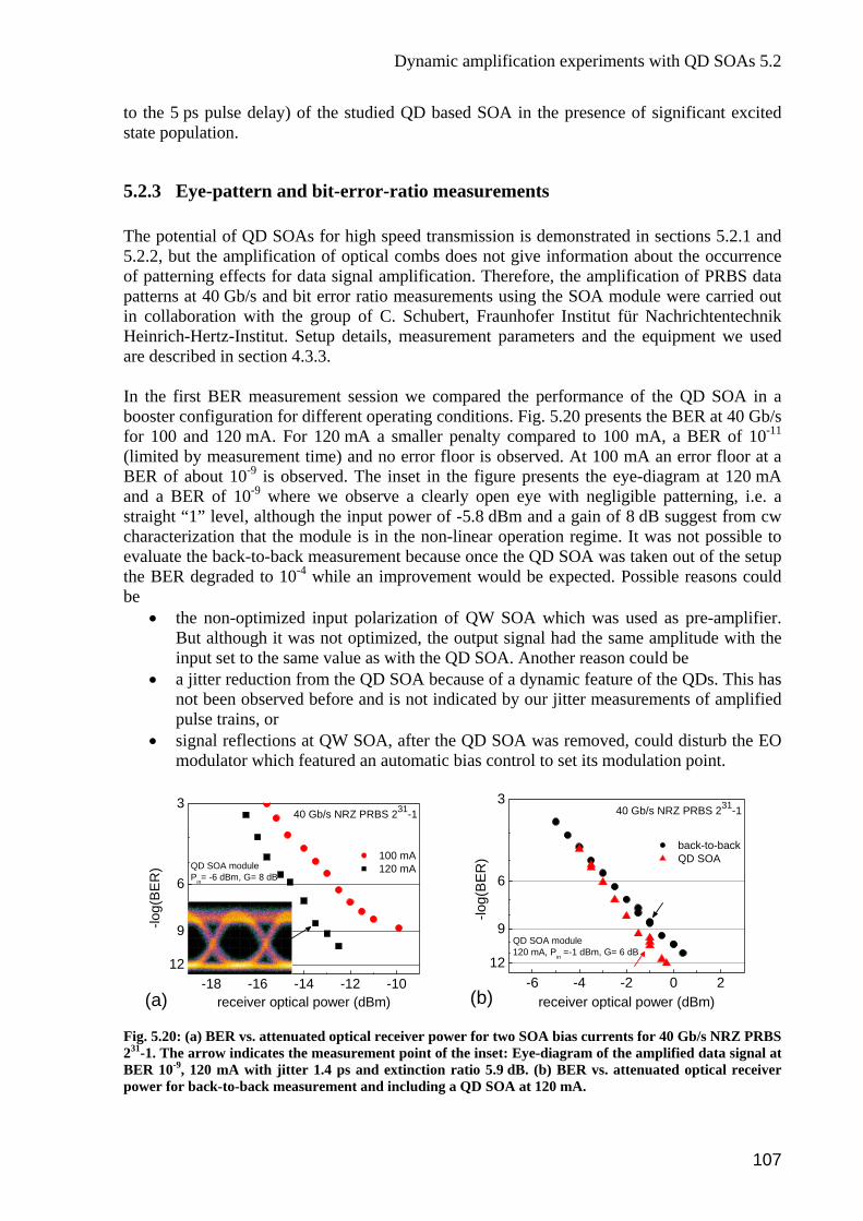
Dynamic amplification experiments with QD SOAs 5.2
to the 5 ps pulse delay) of the studied QD based SOA in the presence of significant excited state population.
5.2.3 Eye-pattern and bit-error-ratio measurements
onstrated in sections 5.2.1 and formation about the occurrence
f patterning effects for data signal amplification. Therefore, the amplification of PRBS data
easurement session we compared the performance of the QD SOA in a ooster configuration for different operating conditions. Fig. 5.20 presents the BER at 40 Gb/s
Possible reasons could e
• the non-optimized input polarization of QW SOA which was used as pre-amplifier. But although it was not optimized, the output signal had the same amplitude with the input set to the same value as with the QD SOA. Another reason could be
• a jitter reduction from the QD SOA because of a dynamic feature of the QDs. This has not been observed before and is not indicated by our jitter measurements of amplified pulse trains, or
• signal reflections at QW SOA, after the QD SOA was removed, could disturb the EO modulator which featured an automatic bias control to set its modulation point.
The potential of QD SOAs for high speed transmission is dem5.2.2, but the amplification of optical combs does not give inopatterns at 40 Gb/s and bit error ratio measurements using the SOA module were carried out in collaboration with the group of C. Schubert, Fraunhofer Institut für Nachrichtentechnik Heinrich-Hertz-Institut. Setup details, measurement parameters and the equipment we used are described in section 4.3.3. In the first BER mbfor 100 and 120 mA. For 120 mA a smaller penalty compared to 100 mA, a BER of 10-11 (limited by measurement time) and no error floor is observed. At 100 mA an error floor at a BER of about 10-9 is observed. The inset in the figure presents the eye-diagram at 120 mA and a BER of 10-9 where we observe a clearly open eye with negligible patterning, i.e. a straight “1” level, although the input power of -5.8 dBm and a gain of 8 dB suggest from cw characterization that the module is in the non-linear operation regime. It was not possible to evaluate the back-to-back measurement because once the QD SOA was taken out of the setup the BER degraded to 10-4 while an improvement would be expected.b
-18 -16 -14 -12 -1012
9
6
3
QD SOA modulePin= -6 dBm, G= 8 dB
40 Gb/s NRZ PRBS 231-1
100 mA 120 mA
-log(
BE
R)
receiver optical power (dBm)(a)-6 -4 -2 0 2
12
9
6
3
-log(
BE
R)
receiver optical power (dBm)
back-to-back QD SOA
QD SOA module120 mA, Pin =-1 dBm, G= 6 dB
40 Gb/s NRZ PRBS 231-1
(b)
Fig. 5.20: (a) BER vs. attenuated optical receiver power for two SOA bias currents for 40 Gb/s NRZ PRBS 231-1. The arrow indicates the measurement point of the inset: Eye-diagram of the amplified data signal at BER 10-9, 120 mA with jitter 1.4 ps an xtinct ratio 5.9 dB. (b) BER vs. attenuated optical receiver power for back-to-back measurement and inclu
d e ion ding a QD SOA at 120 mA.
107

5 Application Oriented Experiments with QD SOAs
In the next BER session we modified the setup, used the QW SOA only in the cw part as booster of the ECL, and compensated the sensitivity problem at the receiver side with a broadband electrical amplifier. In this configuration it was possible to measure the back-to-back performance of the setup and compare it with the influence of the QD SOA module. The BER traces of back-to-back and QD SOA are concurrent within error margins (Fig. 5.20b) and we observe error-free transmission down to a BER of 10-12. The QD SOA exhibits even a small negative penalty, but that is compensated by its degraded optical signal to noise ratio as
would be ideal to unctiocan be inferred from the eye-diagrams presented in Fig. 5.21. In a next measurement session it
compare the BER as a f n of optical SNR to undermine this conclusion. The degraded optical SNR stems from an increased patterning which we observe in the eye-diagram at a BER of 5·10-11 when the amplifier is driven at 120 mA and in saturation with an optical input power of -1 dBm.
0
5
10
15
0 20 40 60 80 100
BER 3·10-9 @ -1 dBm receiver optical power
sign
al le
vel (
mV
)
back-to-back
5
15
time (ps)(a)
10
0 20 40 60 80 1000
(b)
BER 5·10-11 @ -1 dBm receiver optical power
DO520 modul bar2_1 05A
sign
al le
vel (
mV
)
QD SOA
time (ps)
Fig. 5.21: Eye diagrams 40 Gb/s NRZ PRBS 231-1 corresponding to a BER data point of Fig. 5.20-b (indicated by an arrow) at -1 dBm receiver optical power. (a) back-to-back transmission, BER 3·10-9 (b) QD SOA amplification, BER 5·10-11 The patterning dependence was further investigated by recording the direct patterns after amplification with the QD SOA for different input powers with a 70 GHz sampling oscilloscope. The same pattern sections from a 40 Gb/s NRZ PRBS with 27-1 bit length are depicted in Fig. 5.22 for strongly saturating input (+3.5 dBm) and for -4 dBm which is close to the cw 3dB saturation input power of -5 dBm. In the first case large overshoots of the ones Ipeak after a gain recovery during the zero levels are found which relax to a saturated “1” intensity Isat. In the case with lower input power we find no such overshoot, the remaining patterns are also observed in the back-to-back measurement.
(a) (b) Fig. 5.22: Patterning effects after amplification using the QD SOA in 40 Gb/s NRZ PRBS 27-1 data pattern: 100000001111110111110011110101110001101. Patterns for input power levels of
+3.5 dBm (a) and -4 dBm (b).
108
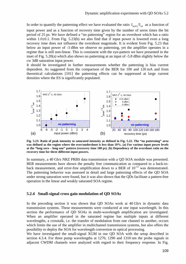
Dynamic amplification experiments with QD SOAs 5.2
In order to quantify the patterning effect we have evaluated the ratio peak satI I as a function of input power and as a function of recovery time given by the number of zeros times the bit eriod of 25 ps. We have defined a “no patterning” region for an overshoot which has a ratio
power is lowered even a long t is evident from Fig. 5.23 that
elow an input power of -3 dBm we observe no patterning, yet the amplifier operates in a
icantly populated.
pwithin 1.0±0.1. From Fig. 5.23(b) we also find that if inputrecovery time does not influence the overshoot magnitude. Ibregime that is still non-linear. This is consistent with the eye-pattern we have presented in the inset of Fig. 5.20(a) which also shows no patterning at an input of -5.8 dBm slightly below the cw 3dB saturation input power. It should be investigated in further measurements whether the patterning is bias current dependent. As suggested from the comparison of the BER for 100 and 120 mA and from theoretical calculations [101] the patterning effects can be suppressed at large current densities where the ES is signif
1.0
1.1
1.2
1.31.4
1.5
1.6
1.7
-5 -4 -3 -2 -1 0 1 2 3 4(
I peak
/ I sa
t
NRZ 27-1, 40 Gb/s
no patterning 1.01.11.21.31.41.51.61.7
a) input power (dBm)20 40 60 80 100 120 140 160 180
no patterning
NRZ 27-1, 40 Gb/s
I peak
/ I sa
t
+3.5 dBm 0 dBm -3 dBm
recovery time (ps)(b)
: Ratio of peak intensity to saturated intensity as defined in Fig. 5.22. The “no patterning” area Fig. 5.23was defiat threcovery In sBER m k-to-back measurement, and error-free amplification down to a BER of 10 was demonstrated. The patterning behavior was assessed in detail and large patterning effects of the QD SOA under strong saturation were found, but it was also shown that the QDs facilitate a pattern-free operation in the linear and weakly saturated SOA regime.
5.2.4 Small-signal cross gain modulation of QD SOAs In the preceding section it was shown that QD SOAs work at 40 Gb/s in dynamic data transmission systems. These measurements were conducted at one input wavelength. In this section the performance of QD SOAs in multi-wavelength amplification are investigated. When an amplifier operated in the saturated regime has multiple inputs at different wavelengths, a crosstalk, i.e. the transfer of modulation from one channel to another, occur
ction 4.3.4. For three pump wavelengths at 1270, 1290 and 1310 nm the probe signals in adjacent CWDM channels were analyzed with regard to their frequency response. In Fig.
ned as the region where the over/undershoot is less than 10%. (a) For various input power levels e “long zero – long one” pattern (recovery time 180 ps). (b) Dependency of the overshoot ratio on the
time for three different input powers.
ummary, a 40 Gb/s NRZ PRBS data transmission with a QD SOA module was presented. easurements have shown the penalty free communication as compared to a bac
-12
s which limits the use of the amplifier in multichannel transmission systems, but also offers the possibility to deploy the SOA for wavelength conversion in optical processing. We have investigated the small-signal XGM in our QD SOA with the setup described in se
109
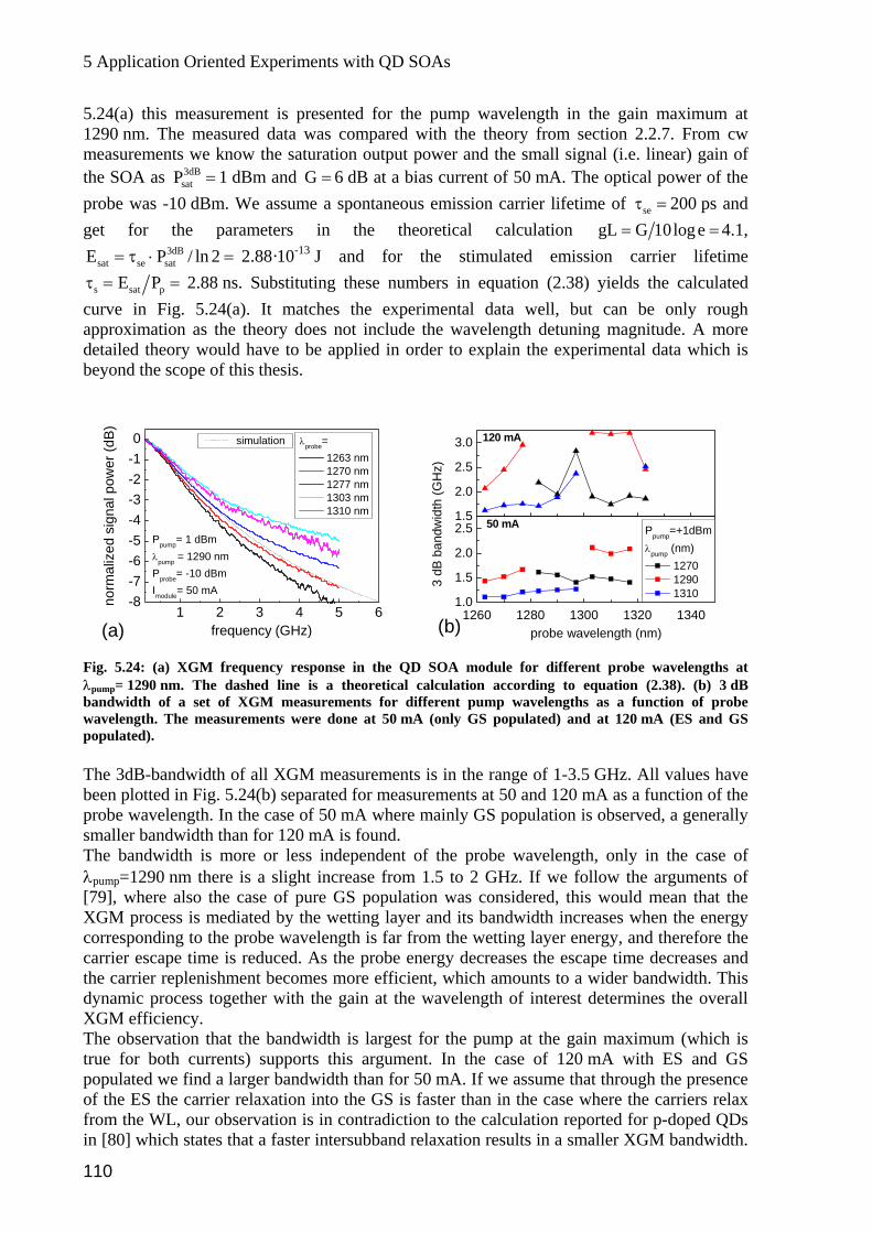
5 Application Oriented Experiments with QD SOAs
5.24(a) this measurement is presented for the pump wavelength in the gain maximum at 1290 nm. The measured data was compared with the theory from section 2.2.7. From cw measurements we know the saturation output power and the small signal (i.e. linear) gain of the SOA as 3dB
satP = 1 dBm and G = 6 dB at a bias current of 50 mA. The optical power of the probe was -10 dBm. We assume a spontaneous emission carrier lifetime of seτ = 200 ps and get for the parameters in the theoretical calculation gL G 10loge= = 4.1,
3dBsat se satE P / ln 2= τ ⋅ = 2.88·10-13 J and for the stimulated emission carrier lifetime
s sat pE Pτ = = 2.88 ns. Substituting these numbers in equation (2.38) yields the calculated curve in Fig. 5.24(a). It matches the experimental data well, but can be only rough approximation as the theory does not include the wavelength detuning magnitude. A more detailed theory would have to be applied in order to explain the experimental data which is beyond the scope of this thesis.
1 2 3 4 5 6-8-7-6-5-4-3-2-10
norm
aliz
ed s
igna
l pow
er (d
B)
frequency (GHz)
λprobe= 1263 nm 1270 nm 1277 nm 1303 nm 1310 nm
Ppump= 1 dBmλpump = 1290 nmPprobe= -10 dBmImodule= 50 mA
simulation
(a)1260 1280 1300 1320 1340
1.0
1.5
2.0
2.51.5
2.0
2.5
3.0
3 dB
ban
dwid
th (G
Hz)
probe wavelength (nm)
Ppump=+1dBmλpump (nm)
1270 1290 1310
50 mA
120 mA
e in the QD SOA module for different probe wavelengths at
he bandwidth is more or less independent of the probe wavelength, only in the case of λpump=1290 nm there is a slight increase from 1.5 to 2 GHz. If we follow the arguments of [79], where also the case of pure GS population was considered, this would mean that the XGM process is mediated by the wetting layer and its bandwidth increases when the energy corresponding to the probe wavelength is far from the wetting layer energy, and therefore the carrier escape time is reduced. As the probe energy decreases the escape time decreases and the carrier replenishment becomes more efficient, which amounts to a wider bandwidth. This dynamic process together with the gain at the wavelength of interest determines the overall XGM efficiency. The observation that the bandwidth is largest for the pump at the gain maximum (which is
the case of 120 mA with ES and Glated we find a larger bandwidth than f A. If we assume that through the presen
lts in a smaller XGM bandwidth.
(b)
ig. 5.24: (a) XGM frequency responsFλpump= 1290 nm. The dashed line is a theoretical calculation according to equation (2.38). (b) 3 dB bandwidth of a set of XGM measurements for different pump wavelengths as a function of probe wavelength. The measurements were done at 50 mA (only GS populated) and at 120 mA (ES and GS populated). The 3dB-bandwidth of all XGM measurements is in the range of 1-3.5 GHz. All values have been plotted in Fig. 5.24(b) separated for measurements at 50 and 120 mA as a function of the probe wavelength. In the case of 50 mA where mainly GS population is observed, a generally smaller bandwidth than for 120 mA is found. T
true for both currents) supports this argument. In S opu or 50 m ce p
of the ES the carrier relaxation into the GS is faster than in the case where the carriers relax from the WL, our observation is in contradiction to the calculation reported for p-doped QDs in [80] which states that a faster intersubband relaxation resu
110
Dynamic amplification experiments with QD SOAs 5.2
Possibly the increase through larger current and stimulated emission shields this effect in our experiment. Note, one data point (at λpump=1270nm, λprobe=1297nm, I=120mA) does not follow the general trend which might be due to a too large probe power having a strong influence in the maximum gain region. In conclusion, we have described small signal XGM in a QD SOA and investigated its modulation bandwidth. We have found only little dependence on the pump-probe wavelength detuning. The largest effect is the increase of the bandwidth with the bias current which is attributed to the presence of the populated ES at larger injection. Our measured bandwidths between 1 and 3.5 GHz are in agreement with other small signal measurements on quantum dot and quantum dash samples and demonstrate the potential for multi-wavelength amplification without crosstalk in the region outside the homogeneous broadening.
111
6 Summary
6 Summary This work is a comprehensive report of the realization and characterization of GaAs based semiconductor optical amplifiers (SOA) using self-organized InGaAs quantu ts (QD) as an active gain medium for optical amplification in the 1.3 µm wavelength
thesis was devoted to simulation and modeling of the device properties like the modal structure of the waveguide, the behavior of tilted waveguides and other means of reduction of the crystal facet reflectivity like anti-reflection coatings or facet windows. These simulations provided the input for design considerations to realize traveling wave amplifiers. The transfer matrix method was a
m do regime.
A part of the
pplied to study the propagation of an optical field through an mplifier. In this model the general gain and saturation behavior of a SOA was illustrated to
understand the propagation dependent mechanisms of the carrier density and the modal gain along the device.
The theory part builds the background to understand the unique properties of the quantum dots and the important characteristics of a semiconductor optical amplifier. SOA relevant features of InGaAs quantum dots like p-doping, the linewidth enhancement factor, inhomogeneous broadening of the emission, gain saturation mechanisms and gain recovery were discussed. Theoretical fundamentals of SOAs were briefly reviewed and the concepts of gain, gain bandwidth, and saturation of gain were explained. The gain ripple, which stems from the residual reflectivity of the Fabry-Perot cavity, was discussed in detail as it causes a wavelength dependent deterioration of the performance of the device. Amplified spontaneous emission is the main origin of noise in the amplifier and adds to the noise figure. These key parameters were investigated considering the influence of polarization and QD properties.
part was topped off with a review on available models for QD SOAs and ubsumed important results that predict excellent performance of QD based SOAs in
of the samples was not a development of this
a
Higher order effects govern the behavior of the SOA in the non-linear gain regime. Cross gain modulation in general and with respect to QDs was described as it is important to explain multi-wavelength cw or dynamic experiments.
The theoryscomparison to conventional SOAs.
The growth of QDs and the epitaxial structurework; the QD samples were optimized for 1.3 µm laser applications, but suited also for the first time realization of SOAs and their use. For future improvement of the QD SOA performance the growth of the quantum dot gain medium and the waveguide structure of the devices need to be tailored to the specific amplifier requirements like large bandwidth, polarization independence and low far field divergence for high coupling efficiencies.
In order to realize a single mode amplifier with a strong guiding of the input signal, the narrow ridge waveguide processing applied for QD lasers was re-designed. With the new processing scheme deeply dry etched (through the active layer) ridge waveguides were realized and a new top contact scheme was implemented enabling easy access to the top contacts with a ground-signal-ground probe head. This allowed for quick bar testing without the need of wire-bonding and was successfully adopted for contacting high speed lasers for direct modulation or hybrid mode-locking applications as well. The processed ridge waveguides feature a natural reflectivity from the crystal end facets, which needed to be suppressed to make a traveling wave amplifier. The concept of tilted waveguides in
112
Summary 6
combination with two-layer anti-reflection coatings was applied and reflectivities below 10-3 were achieved. The mounting of the SOA chips was expanded from simple copper heatsinks to test bars with several devices to a full packaging of two devices where temperature controlled fiber-pigtailed SOA modules were realized.
on coating values well below 10 . The coupling losses from the fiber to the waveguide determined the
et amplifier performance from fiber input to fiber output. The lowest coupling loss to our µm wide ridge waveguide structure was 4 dB using a tapered fiber, which is a good value
for ridge waveguide structures, but far from values below 1 dB that are achieved with buried heterostructures.
The cw performance of the QD SOAs was comparable to commercial QW based amplifiers at 1.3 µm with a chip gain up to 25 dB limited by the onset of lasing, a spectral amplifier bandwidth of 30 nm indicating that these QDs were relatively homogeneous in size, and a minimum chip noise figure of 4 dB which was close to the theoretical limit of 3 dB. In the linear regime of the QD SOA, i.e. at low input power, negligible influence of three CWDM wavelengths amplified in the SOA was found, which shows the potential for multi-wavelength data transmission.
The ASE cross gain measurement displayed a spectral hole with a shallow slope since carrier replenishment in a particular saturated QD group originated from other, spectrally neighboring, QD groups, which is typical for an inhomogeneously broadened gain medium. Polarization resolved measurements evidenced a polarization ratio of 6-8 dB. This dominant TE polarization was expected from the modeling of the decoupled QD layers. The rectangular ridge waveguide also favors TE polarized light. Modeling of QD polarization dependence showed that it should be possible to achieve polarization insensitive SOAs with a balanced TE/TM ratio using vertically coupled QD stacks.
In dynamic measurements the QD SOAs demonstrated excellent performance. The amplification of fast pulse trains from mode-locked lasers with identical QD gain medium, repetition frequencies from 20 to 80 GHz, and pulse widths as short as 710 fs was investigated. Thereby, insight in the capabilities of the QD SOA to amplify a high speed pulse sequence was gained. The mode-locked pulse trains were essentially undistorted by the amplifier and only a small increase of the auto-correlation pulse width was observed at high repetition rates of 40 and 80 GHz. The broadening of the pulses at these frequencies was attributed to the 2nd slower term in the bi-exponential recovery of the QD SOA gain which is on the order of 10-100 ps, implying a broadening of the pulses at repetition rates larger than 10-100 GHz. These results emphasize the potential of ultrafast dynamics of QD SOAs for their application in optical high-bitrate transmission systems. Ultrafast amplification at 80 GHz and excellent jitter performance make QD SOAs ideal candidates for future 100 GBit Ethernet.
Using ultrafast pump-probe spectroscopy the gain recovery dynamics in a QD based SOA after amplification of double femtosecond pump pulses was investigated. A distinct change in gain recovery in the ground state was observed when a significant excited state population
The amplifiers were characterized and optimized with regard to their internal device performance. The far field measurement verified that by processing ridges with only 1 µm width a quasi-symmetric far field was realized, which minimizes coupling losses due to mode ellipticity. Using the Hakki-Paoli method the gain-reflectivity product from the ASE ripple of the spectrum was measured. In combination with a spectrally resolved gain measurement we were able to evaluate the combined reflectivity of tilted waveguide and anti-reflecti
-3ton4
113
6 Summary
was achieved. A compdelay passed through th
lete gain recovery was found when two 150 fs pulses with 5 ps time e SOA in resonance to the ground state under high injection currents
f 80 to 100 mA. The results indicate that the overall gain recovery dynamics were
A was investigated. Only little dependence on the pump-probe wavelength detuning was und. The largest effect was the increase of the bandwidth with the bias current, which was
ut the QD SOA, and error-free amplification down to a BER of 10-12 was
l-optical signal processing.
oaccelerated in the presence of significant excited state population. This opens the way for ultrafast (> 200 GHz) operation in p-doped QD based SOAs at 1.3 µm telecom wavelengths.
With measurements of small signal cross gain modulation, the modulation bandwidth in a QD SOfoattributed to the presence of the populated ES at larger injection. The measured XGM bandwidths between 1 and 3.5 GHz were in agreement with other small signal measurements on quantum dot and quantum dash samples and demonstrate the potential for multi-wavelength amplification without crosstalk in the region outside the homogeneous broadening of the QDs.
A 40 Gb/s NRZ PRBS data transmission with a QD SOA module was measured. Bit-error-ratio measurements showed penalty free communication as compared to a back-to-back measurement withodemonstrated. The patterning behavior was assessed in detail and large patterning effects of the QD SOA under strong saturation were found, but it was also shown that the QDs facilitate a pattern-free operation in the linear and weakly saturated SOA regime.
Despite these encouraging results, the QD SOAs presented in this work still lack from some device limitations like insufficient reduction of reflectivity resulting in the onset of lasing, polarization dependence, and large coupling losses. But these limitations can be overcome by further design improvements, e.g. larger waveguide tilt angle and growth modifications like coupled QD stacks and re-growth for buried heterostructures, respectively. The dynamic behavior of the quantum dot based SOAs was proven to be state of the art enabling ultrafast, beyond 100 GHz operation at 1.3 µm telecom wavelengths. Using QDs as a gain medium opens up the road for future high speed all-optical networks employing QD SOAs as ultrafast amplifying elements or functional elements in al
114

Abbreviations and acronyms 7.1
7 Technical Annex 7.1 Abbreviations and acronyms The following table shows the abbreviations and acronyms used in this text.
1D, 2D, 3D One-, two-, three-dimensional PBC Photonic bandgap crystal 3R Re-amplification, re-shaping, re-timing PD Photodetector AC Auto-correlation PRBS Pseudo random bit sequence AMP Electrical amplifier PWM Powermeter AR Anti-reflection QD Quantum dot ASE Amplified spontaneous emission QDash Quantum dash ATT Attenuator QW Quantum well BCB Bencocyclobutene RHEED Reflection high energy electron diffraction BER(T) Bit error ratio (tester) RIE Reactive ion etching BPG Bit pattern generator RTA Rapid thermal annealing BPM Beam propagation method RZ Return to zero CAIBE Chemical assisted ion beam etching SC Separate confinement CAD Computer aided design SEM Scanning electron microscope CWDM Coarse wavelength division multiplexer SGM Self gain modulation DC BIAS Direct current bias SHG Second harmonic generation DEMUX De-Multiplexer SMF Single mode fiber DHS Double heterostructure SNR Signal to noise ratio DI Direct interpolation SOA Semiconductor optical amplifier DWELL Dots-in-a-well SOG Spin-on glass ECL External cavity laser SPM Self phase modulation EOM Electro optical modulator SSE Source spontaneous emission ES Excited state T-Control Temperature control ESA Electrical spectrum analyzer TE Transverse electric FBH Ferdinand Braun Institut für
Höchstfrequenzmesstechnik TEM Transmission electron microscope
FWHM Full width at half maximum TM Transverse magnetic FWM Four wave mixing TMM Transfer matrix method GPIB General purpose interface bus TU(B) Technische Universität (Berlin) GS Ground state VOA Variable optical attenuator GSG Ground-signal-ground WL Wetting layer HH Heavy hole XGM Cross gain modulation HRI High refractive index (material) XPM Cross phase modulation LH Light hole LOC Large optical cavity LRI Low refractive index (material) MBE Molecular beam epitaxy ML Monolayer MOCVD Metal organic chemical vapor
deposition
MPI Multi-path interference MUX Multiplexer NF Noise figure NRZ Non return to zero OSA Optical spectrum analyzer
115
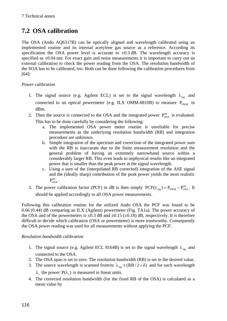
7 Technical annex
7.2 OSA calibration The OSA (Ando AQ6317B) can be optically aligned and wavelength calibrated using an implemented routine and its internal acetylene gas source as a reference. According its specification the OSA power level is accurate to ±0.3 dB. The wavelength accuracy is
ignal source (e.g. Agilent ECL) is set to the signal wavelength and
procedure are unknown.
P P= − . It should be applied accordingly to all OSA power measurements.
Following this calibration routine for the utilized Ando OSA the PCF was found to be 0.66 (0.44) dB comparing an ILX (Agilent) powermeter (Fig. TA1a). The power accuracy of the OSA and of the powermeters is ±0.3 dB and ±0.15 (±0.18) dB, respectively. It is therefore difficult to decide which calibration (OSA or powermeter) is more trustworthy. Consequently the OSA power reading was used for all measurements without applying the PCF. Resolution bandwidth calibration
1. The signal source (e.g. Agilent ECL 8164B) is set to the signal wavelength and connected to the OSA.
2. The OSA span is set to zero. The resolution bandwidth (RB) is set to the desired value. 3. The source wavelength is scanned from/to
specified as ±0.04 nm. For exact gain and noise measurements it is important to carry out an external calibration to check the power reading from the OSA. The resolution bandwidth of the SOA has to be calibrated, too. Both can be done following the calibration procedures from [64]: Power calibration
1. The s sigλ
connected to an optical powermeter (e.g. ILX OMM-6810B) to measure PWMP in dBm.
2. Then the source is connected to the OSA and the integrated power intOSAP is evaluated.
This has to be done carefully by considering the following: a. The implemented OSA power meter routine is unreliable for precise
measurements as the underlying resolution bandwidth (RB) and integration
b. Simple integration of the spectrum and correction of the integrated power sum with the RB is inaccurate due to the finite measurement resolution and the general problem of having an extremely narrowband source within a considerably larger RB. This even leads to unphysical results like an integrated power that is smaller than the peak power at the signal wavelength.
c. Using a sum of the (interpolated RB corrected) integration of the ASE signal and the (ideally sharp) contribution of the peak power yields the most realistic
intOSAP .
3. The power calibration factor (PCF) in dB is then simply PCF( )λ intsig PWM OSA
sigλ
sig (RB / 2 )λ ± + δ and for each wavelength the power is measured in linear units.
4. The corrected resolution bandwidth (for the fixed RB of the OSA) is calculated as a mean value by
iλ iP( )λ
116
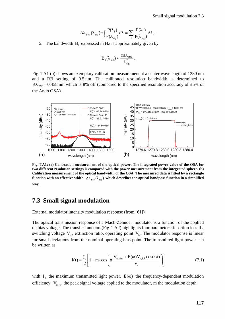
Small signal modulation 7.3
BW sig(∆λ λ i ii
isig sig
P( ) P( ))= d
P( ) P( )λ λ
λ = ∆λλ λ∑∫ .
ximately given by 5. The bandwidth 0B expressed in Hz is appro
BWcB ( )0 sig 2
∆λλ ≈ .
sigλ F e ent at a center wavelength of 1280 nm a RB . The calibrate olutio th is determined to
= 0.458 8% off (compared to the specified resolution accuracy of ±5% of t do OS
ig. TA1 (b) shows an exemplary calibration m asuremnd a setting of 0.5 nm d res n bandwid
BWλ∆ nm which ishe An A).
1279.6 1279.8 1280.0 1280.2 1280.405
101520
354045
2530
OSA
1000 00 1500 1600-80
-70
0
-40
0
-20
1100 1200 1300 14
-60
-5
-3
(a)
inte
nsity
(dB
m)
wavelength (nm)
OSA sens "mid".243 dBmPmid
int = -15 OSA sens "high 1"
mid= -15.217 dBm
= -13 dBm - loss ATT
Pint
PILXPWM= -14.56 dBm
PCF= 0.66 dB
ECλ=Pin
L input 1280 nm
rectangle fcn
OSA sRBW PECL = rough ATT
∆λBW(λ
ettings= 0.5 nm, span = 0 nm, λcenter= 1280 nm 50.12±0.03 µW - loss th
s) = 0.458 nm
inte
nsity
(µW
)
wavelength (nm)(b)
F 1: (a) C the optical power. The in e of the OSA for t nt r d with the power measur . (b) C tion me dwidth of A. The ngle f ith a ) which describes the op n in a simplified w 7 External modulator intensity modulation response (from [61]) T tical t ach-Zehnder modulator is a function of the applied d voltag on (Fig. TA2 highlights ur parameters: insertion loss IL, s vo operating point
ig. TA alibration measurement of e
tegrated power valuwo differealibra
esolution settings is comparasurement of the optical ban
ement from the integrated spheremeasured data is fitted by a rectathe OS
unction w n effective width BW si(∆λ λ g tical bandpass functioay.
.3 Small signal modulation
he opas
ransmission response of a Mc bi e. The transfer functi ) fowitching ltage Vπ , extinction ratio, bV . The modulator response is linear
for small deviations from the nominal operating bias point. The transmitted light power can b
e written as
,bias ,V E( )V cos( t)cos
Vπ π
π
⎡ ⎤+ ω ω⎛ ⎞⋅ π ⎥⎜ ⎟
⎝ ⎠ (7.1)
ith the maximum transmitted light power,
RF0I(t) 1 m2
= +⎢⎣ ⎦
I
w 0I E( )ω the frequency-dependent modulation fficiency, the peak signal voltage applied to the modulator, m the modulation depth. ,RFVπe
117
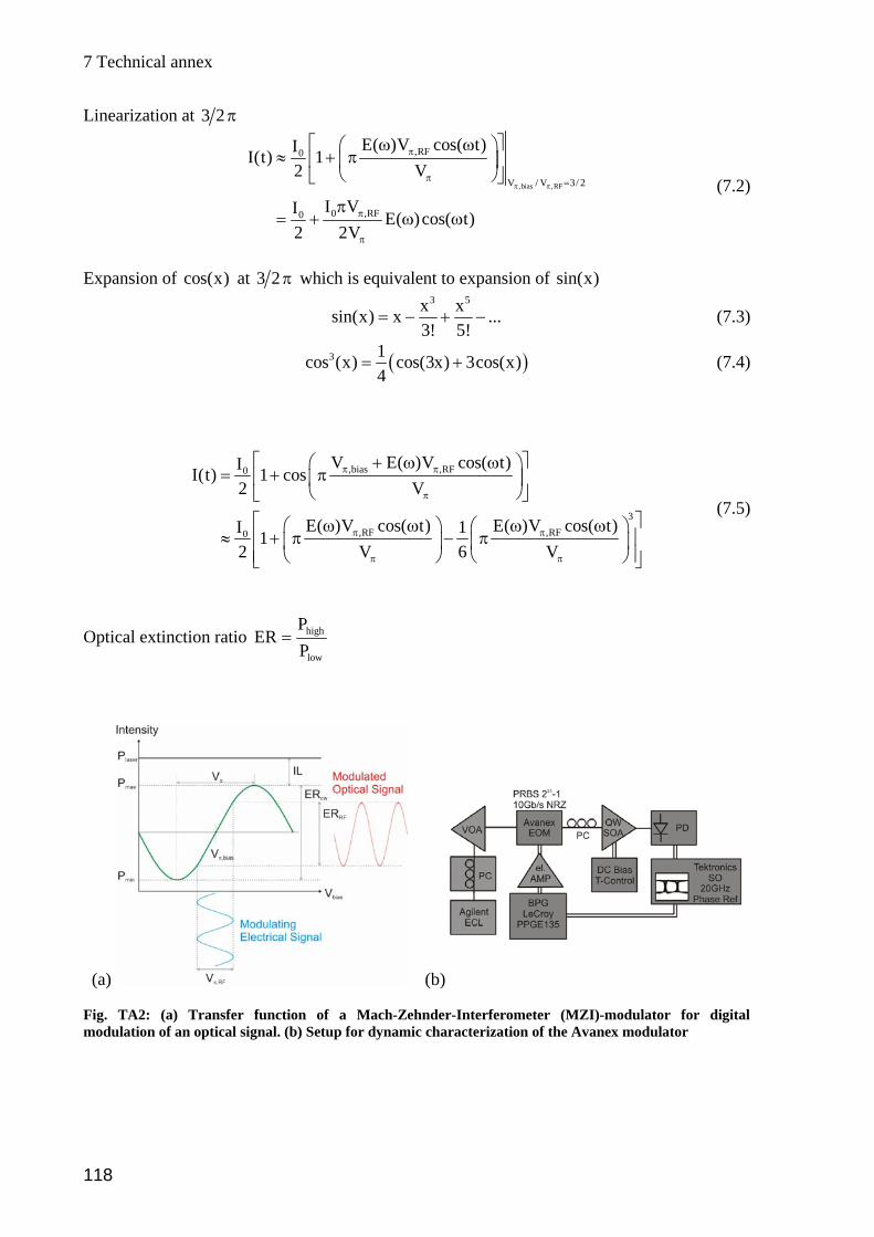
7 Technical annex
Linearization at 3 2 π
,bias ,RF
,RF0
V / V 3/ 2
0 ,RF0
I(t) 12 V
I VI E( )cos( t)2 2V
π π
π
π =
π
π
E( )V cos( t)I ⎡ ⎤ω ω⎛ ⎞≈ + π⎢ ⎥⎜ ⎟
⎝ ⎠ ⎣ ⎦
π= + ω ω
(7.2)
Expansion of cos(x) at which is equivalent to expansion of sin(x) 3 2 π
3 5x xsin(x) x ...3! 5!
= − + − (7.3)
( )3cos (x) cos(3x) 3cos(x)4
= + (7.4) 1
,bias ,RF0 V E( )V cos( t)II(t) 1 cos π π⎡ ⎤+ ω ω
3,R0
2 V
E( )VI
π
π
⎢ ⎥⎜ ⎟⎝ ⎠⎣ ⎦
⎡ ⎤ω⎛≈ + π⎢
(7.5) F ,RFcos( t) E( )V cos( t)1 π1
2 V 6 Vπ π
− π ⎥⎜ ⎟ ⎜ ⎟
⎛ ⎞
ω ω ω⎞ ⎛ ⎞
= + π
⎢ ⎥⎝ ⎠ ⎝ ⎠⎣ ⎦
Optical ext tinc ion ratio highPER =
lowP
(a)
(b) Fig. - erferometer (mod racterization of the
TA2: (a) Transfer function of a Mach-Zehnder MZI)-modulator for digital ulation of an optical signal. (b) Setup for dynamic cha Avanex modulator
Int
118
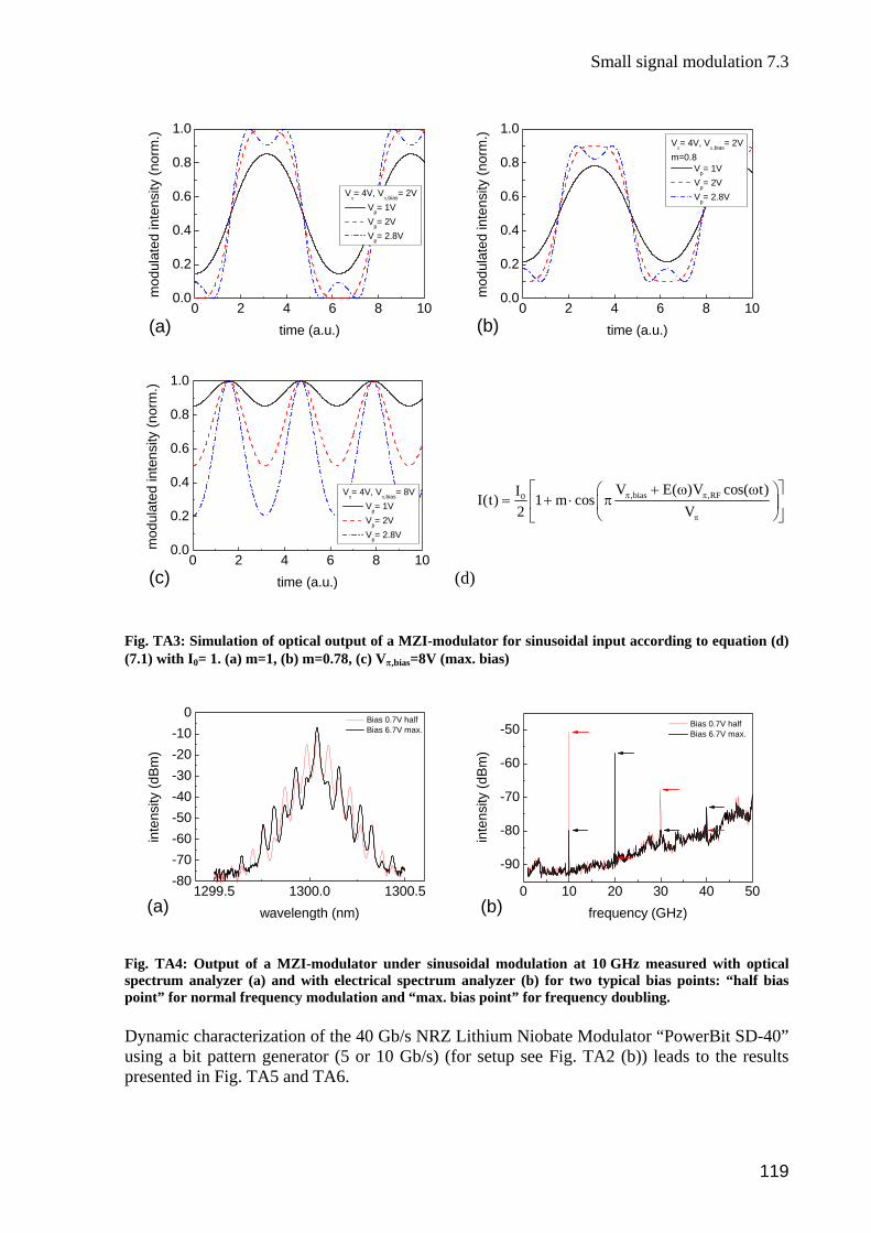
Small signal modulation 7.3
0
1.0
0 2 4 6 8 100.0
0.2
0.4
0.6
.8
ted
inte
nsity
(nor
m.)
mod
ula
time (a.u.)
Vπ= 4V, V
π,bias= 2V Vp= 1V Vp= 2V Vp= 2.8V
(a)
1.0
0 2 4 6 8 100.0
0.2
0.4
0.6
0.8
ted
inte
nsor
m.) V
π= 4V, V
π,bias= 2Vm=0.8
Vp= 1V
ity (n
Vp= 2V Vp= 2.8V
mod
ula
time (a.u.)(b)
0 2 4 6 8 100.0
0.2
0.4
0.6
0.8
1.0
(c)
mod
ulat
ed in
tens
ity (n
orm
.)
time (a.u.)
Vπ= 4V, V
π,bias= 8V Vp= 1V Vp= 2V Vp= 2.8V
(d)
,bias ,RF0 V E( )V cos( t)II(t) 1 m cos2 V
π π
π
⎡ ⎤+ ω ω⎛ ⎞= + ⋅ π⎢ ⎥⎜ ⎟
⎝ ⎠⎣ ⎦
Fig. TA3: Simulation of optical output of a MZI-modulator for sinusoidal input according to equation (d) (7.1) with I0= 1. (a) m=1, (b) m=0.78, (c) Vπ,bias=8V (max. bias)
-40
-100
1299.5 1300.0 1300.5-80-70-60-50
-30-20
Bias 0.7V half Bias 6.7V max.
inity
(te
ns
-80
dBm
)
wavelength (nm)(a)0 10 20 30 40 50
-90
-70
-60
-50 Bias 0.7V half Bias 6.7V max.
inte
nsity
(dB
m)
frequency (GHz)(b)
Fspectrum analyz
ig. TA4: Output of a MZI-modulator under sinusoidal modulation at 10 GHz measured with optical er (a) and with electrical spectrum analyzer (b) for two typical bias points: “half bias
oint” for normal frequency modulation and “max. bias point” for frequency dou
ynamic characterization of the 40 Gb/s NRZ Lithium Niobate Modulator “PowerBit SD-40”
p bling. Dusing a bit pattern generator (5 or 10 Gb/s) (for setup see Fig. TA2 (b)) leads to the results presented in Fig. TA5 and TA6.
119
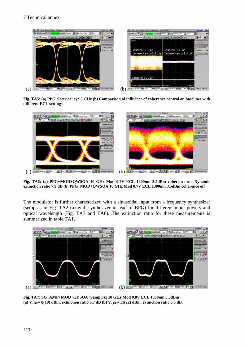
7 Technical annex
(a) (b)
ig. TA5: (a) PPG electrical eye 5 GHz (b) Comparison of influence of ifferent ECL settings
(a)
F coherence control on baselines with d
(b) Fig. TA6: (a) PPG+MOD+QWSOA 10 GHz Mod 0.7V ECL 1300nm 3.5dBm coherence on. Dynamic xtinction ratio 7.9 dB (b) PPG+MOD+QWSOA 10 GHz Mod 0.7V ECL 1300nm 3.5dBm coherence off
The modulator is further characterized with a sinusoidal input from a frequency synthesizer (setup as in Fig. TA2 (a) with synthesizer instead of BPG) for different input powers and optical wavelength (Fig. TA7 and TA8). The extinction ratio for these measurements is summarized in table TA1.
e
(a) (b) Fig. TA7: SG+AMP+MOD+QDSOA+SampOsz 10 GHz Mod 0.8V ECL 1300nm 3.5dBm (a) Vπ,RF= 8(19) dBm, extinction ratio 5.7 dB (b) Vπ,RF= 11(22) dBm, extinction ratio 5.5 dB.
120
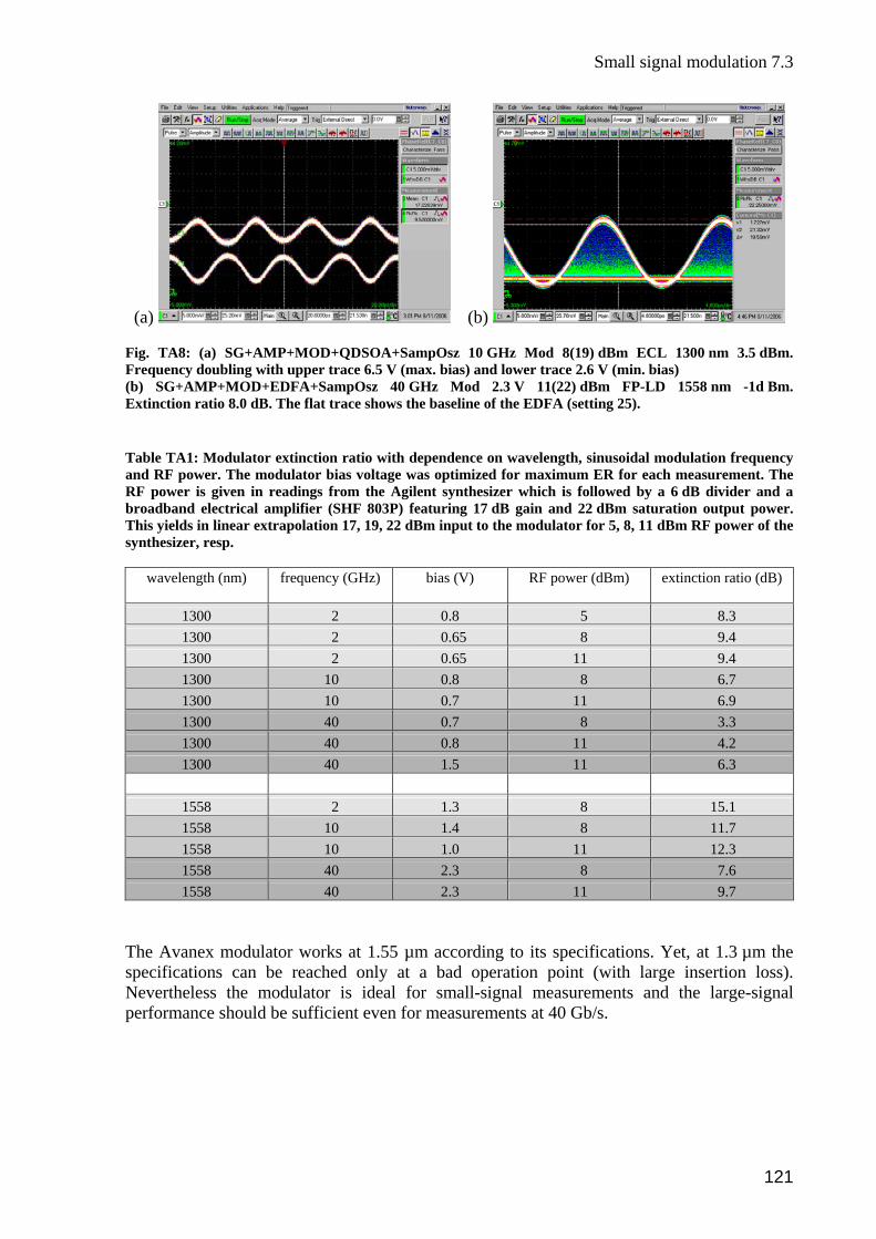
Small signal modulation 7.3
(a) (b) Fig. TA8: (a) SG+AMP+MOD+QDSOA+SampOsz 10 GHz Mod 8(19) dBm ECL 1300 nm 3.5 dBm. Frequency doubling with upper trace 6.5 V (max. bias) and lower trace 2.6 V (min. bias) (b) SG+AMP+MOD+EDFA+SampOsz 40 GHz Mod 2.3 V 11(22) dBm FP-LD 1558 nm -1d Bm. Extinction ratio 8.0 dB. The flat trace shows the baseline of the EDFA (setting 25). Table TA1: Modulator extinction ratio with dependence on wavelength, sinusoidal modulation frequency and RF power. The modulator bias voltage was optimized for maximum ER for each measurement. The RF power is given in readings from the Agilent synthesizer which is followed by a 6 dB divider and a broadband electrical amplifier (SHF 803P) featuring 17 dB gain and 22 dBm saturation output power. This yields in linear extrapolation 17, 19, 22 dBm input to the modulator for 5, 8, 11 dBm RF power of the synthesizer, resp.
wavelength (nm) frequency (GHz) bias ( RF power (dBm) extinction ratio (dB)
V)
1300 2 0.8 5 8.3 1300 2 0.65 8 9.4 1300 2 0.65 11 9.4 1300 10 0.8 8 6.7 1300 10 0.7 11 6.9 1300 40 0.7 8 3.3 1300 40 0.8 11 4.2 1300 40 1.5 11 6.3
1558 2 1.3 8 15.1 1558 10 1.4 8 11.7 1558 10 1.0 11 12.3 1558 40 2.3 8 7.6 1558 40 2.3 11 9.7
he Avanex modulator works at 1.55 µm according to its specifications. Yet, at 1.3 µm the Tspecifications can be reached only at a bad operation point (with large insertion loss). Nevertheless the modulator is ideal for small-signal measurements and the large-signal erformance should be sufficient even for measurements at 40 Gb/s. p
121
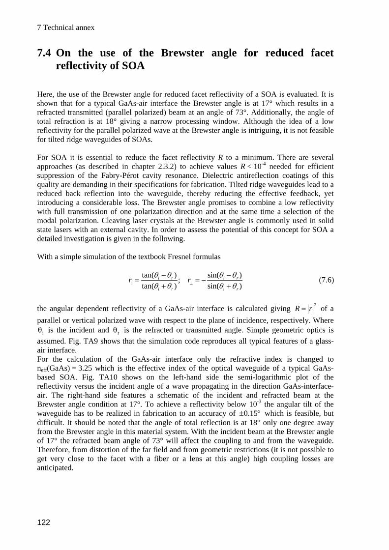
7 Technical annex
7.4 On the use of the Brewster angle for reduced facet reflectivity of SOA
Here, the use of the Brewster angle for reduced facet reflectivity of a SOA is evaluated. It is shown that for a typical GaAs-air interface the Brewster angle is at 17° which results in a refracted transmitted (parallel polarized) beam at an angle of 73°. Additionally, the angle of total refraction is at 18° giving a narrow processing window. Although the idea of a low reflectivity for the parallel polarized wave at the Brewster angle is intriguing, it is not feasible
ibed in chapter 2.3.2) to achieve values R < 10-4 needed for efficient uppression of the Fabry-Pérot cavity resonance. Dielectric antireflection coatings of this
quality are demanding in their specifications for fabrication. Tilted ridge waveguides lead to a reduced back reflection into the waveguide, thereby reducing the effective feedback, yet introducing a considerable loss. The Brewster angle promises to combine a low reflectivity with full transmission of one polarization direction and at the same time a selection of the modal polarization. Cleaving laser crystals at the Brewster angle is commonly used in solid state lasers with an external cavity. In order to assess the potential of this concept for SOA a detailed investigation is given in the following. With a simple simulation of the textbook Fresnel formulas
for tilted ridge waveguides of SOAs. For SOA it is essential to reduce the facet reflectivity R to a minimum. There are several approaches (as descrs
tan( ) sin( ); tan( ) sin( )⊥
− −= = −i r i rr rθ θ θ θ
+ +i r i rθ θ θ θ
(7.6)
e angular dependent reflectivity of a GaAs-air interface is calculated giving 2R r=th of a
or the calculation of the GaAs-air interface only the refractive index is changed to neff(GaAs) = 3.25 which is the effective index of the optical waveguide of a typical GaAs-based SOA. Fig. TA10 shows on the left-hand side the semi-logarithmic plot of the reflectivity versus the incident angle of a wave propagating in the direction GaAs-interface-air. The right-hand side features a schematic of the incident and refracted beam at the Brewster angle condition at 17°. To achieve a reflectivity below 10-3 the angular tilt of the waveguide has to be realized in fabrication to an accuracy of
parallel or vertical polarized wave with respect to the plane of incidence, respectively. Where iθ is the incident and rθ is the refracted or transmitted angle. Simple geometric optics is
assumed. Fig. TA9 shows that the simulation code reproduces all typical features of a glass-air interface. F
0.15± ° which is feasible, but difficult. It should be noted that the angle of total reflection is at 18° only one degree away from the Brewster angle in this material system. With the incident beam at the Brewster angle of 17° the refracted beam angle of 73° will affect the coupling to and from the waveguide. Therefore, from distortion of the far field and eometric restrictions (it is not possible to
acet with a fiber or at this angle) high coupling losses are from ga lensget very close to the f
anticipated.
122
Fabry-Perot formulation of the amplifier gain 7.5
0 10 20 30 40 50 60 70 800.0
0.2
0.4
0.6
0.8
1.0
0
20
40
60
80
Fresnel reflectivity: glass - airR θBr
θr
parallel
vertical
n (glass)i
n (air)r
refr
acte
d an
gle
θ r (°)
nr = 1 airni = 1.5 glassθTR = 42 °θBr = 34 °
vertical pol. parallel pol.
incident angle θi (°)
Fig. TA9: Modeling of the well known glass-air interface with the Fresnel formulas (left) and schematic of
0
the Brewster condition (right). The simulation code reproduces all features such as the total refraction angle TRθ = 42°, Brewster angle Brθ = 34° and normal incidence reflectivity of 4%.
1
0 2 4 6 8 10 12 14 16 18 201E-3
.01
0.1
0
20
40
60
80
l reflectivity: GaAs - air
R
incide e θi (°)
Fresne parallel polarization = TE vertical polarization = TM
ni(GaAseff) = 3.25
r(air) = 1
TR = 18°
Br = 17° with θr = 73°
refr
acte
d an
gle
θr (
°)
nθ
θ
θBr
θrpara
nt angl
llel
vertic
n aAs)
r)
Fig. TA1 deling of the Ga ir interface (left) and schematic of Brewster conditio ht). The reflectiv lotted semi-loga mic to indicate small angular acceptance of low reflec y at the Brewster
lthough tilted ridge waveguides (typically 5-10° tilt angle) are commonly used as a means to
.5 Fabry-Perot formulation of the amplifier gain
e follow the derivation of [61] considering a uniform gain profile with a single-pass gain along an amplifier. The output electric field is a sum of multiple reflected signals at
e facets of the cavity with reflections and the geometric mean reflectivity
al
(Gi
n (air
0: Mo As-a the n (rigity is p rith the tivit angle.
Areduce laser feedback from facet reflectivity, it can be clearly seen from this evaluation that the use of the Brewster angle is not feasible for GaAs-based SOA. 7 WG outEs
1,2R 1 2R R R= th
123
7 Technical annex
out 1E (1 R )(1 R= − − 2 s 0
21 2 s 1 2 s
)G E exp( i L)
1 R R G exp( 2i L) R R G exp( 4i L)
− β
⎡ ⎤× + − β + − β +⎣ ⎦ (7.7)
Using the sum for an infinite geometric progression n
n
x 1 (1 x)= −∑ this expression
simplifies to
1 2 s 0out
s 1 2
(1 R )(1 R )G E exp( i L)E
− − − β=
1 G R R exp( 2i L)− − β. (7.8)
Then the output power equals
[ ]
22 i L 22 1 2 s 0 1 2 s 0
out 2 2
s 1 2 s 1 2
(1 R )(1 R )G E e (1 R )(1 R )G EE1 G R R exp( 2i L) 1 G R R cos( 2 L) isin( 2 L)
− β− − − −= =
− − β − − β + − β (7.9)
using the well-known relations ie 1φ = and Eulers formula ie cos isinφ = φ + φ . We use
2 2a x iy x y= + = + to calculate the absolute value of the complex denominator
22 1 2 s 0
out 22
sin( 2 L)2
s 1 2 s 1 2
(1 R )(1 R )G EE1 G R R cos( 2 L) G R R
− −=
⎡ ⎤ ⎡− − β +
(7.10) ⎤− β⎣ ⎦ ⎣ ⎦
Further simplifications of the expression make use of 2 2(cos sin ) 1φ + and φ =
2 12sin (1 cos2 )φ = − φ , as well as 2 2 2(1 2b b ) (1 b)− + = −
2
2 1 2 s 0out
(1 R )(1 R )G EE − −= 2 2
2 2 2 2s 1 2 s 1 2 s 1 2
2 2 2s 1 2 s 1 2
s 1 2 s 1 2 s 1 2
2s 1 2 s
1 2G R R cos( 2 L) G R R cos ( 2 L) G R R sin ( 2 L)
1 G R R (cos ( 2 L) sin ( 2 L)) 2G R R cos( 2 L)
(1 2G R R G R R ) 2G R R (1 cos( 2 L))
(1 G R R ) 4G
⎡ ⎤ ⎡ ⎤− − β + − β + − β⎢ ⎥ ⎢ ⎥⎣ ⎦ ⎣ ⎦
=+ − β + − β − − β
=− + + − − β
=− +
∼
∼
∼2
1 2R R sin ( L)β
(7.11) Now the amplifier gain is given using 2 2E Ein 0= by
2
out 1 2 s2 2
in s 1 2 s 1 2
E (1 R )(1 R )GGE (1 G R R ) 4G R R sin ( L)
− −= =
− + β (7.12)
124
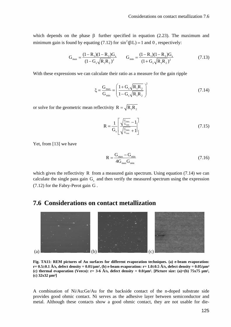
Considerations on contact metallization 7.6
which depends on the phase further specified in equation (2.23). The maximum and minimum gain is found by equating (7.12) for , respectively:
β2sin ( L) 1 and 0β =
1 2 s 1 2max min2 2
s 1 2 s 1 2
(1 R )(1 R )G (1 R )(1 R )GG G(1 G R R ) (1 G R R )− − − −
= =− +
s (7.13)
With these expressions we can calculate their ratio as a measure for the gain ripple
2
s 1 2max
min s 1 2
1 G R RGG 1 G R R
⎛ ⎞+ξ = = ⎜ ⎟⎜ ⎟−⎝ ⎠
(7.14)
or solve for the geometric mean reflectivity 1 2R R R=
max
min
max
GG
G
11RG
mins G 1
⎡ ⎤−⎢ ⎥=⎢ ⎥+⎣ ⎦
(7.15)
Yet, from [13] we have
max min
max min
G GR4G G
−= (7.16)
which gives the reflectivity from a measured gain spectrum. Using equation (7.14) we can calculate the single pass gain and then verify the measured spectrum using the expression (7.12) for the Fabry-Perot gain . 7.6 Considerations on contact metallization
RsG G
(a) (b) (c) Fr=
ig. TA11: REM pictures of Au surfaces for different evaporation techniques. (a) e-beam evaporation: ty = 0.05/µm²
a)+(b) 75x75 µm²,
A ide contact of the n-doped substrate side nductor an
metal. Although these contacts show a good ohmic contact, they are not usable for die-
0.5±0.1 Å/s, defect density = 0.01/µm², (b) e-beam evaporation: r= 1.0±0.5 Å/s, defect densi(c) thermal evaporation (Veeco): r= 3-6 Å/s, defect density = 0.0/µm². [Picture size: (c) 32x32 µm²] (
combination of Ni/Au:Ge/Au for the backsprovides good ohmic contact. Ni serves as the adhesive layer between semico d
125

7 Technical annex
bonding on a diamond heat spreader. During bonding an unknown process – most probably out-diffusion of Ge – prevents a solid connection between the sample and the gold plated iamond. We have tested a number of different n-contacts with the transmis
[193] for their conductivity after rapid thermal annealing (RTA) and checked their suitability r die-bonding as summarized in Table 9.
del) and die-bond
Thicknesses (nm) RTA Contact
d sion line model
fo Table 9: n-contacts tested for conductivity (with transmission line mo ing suitability
Contact
Ni/Au:Ge/Au 8/80/200 390°, 100s Ohmic Standard contact TU (*) Ti/Pt/Au 20/100/200 390°, 100s Schottky Ti/Pt/Au 20/100/200 450°, 90s Schottky Kirstädter [186] (*) Ni/Au:Ge/Ti/Pt/Au 8/45/10/100/200 390°, 100s Semi-Schottky, Stripewidth-dependent (*)
/200 390°, 100s Semi-Schottky (**)
Standard contact HHI (*)
Ni/Au:Ge/Ti/Pt/Au 8/80/10/100
(*) With this contact no stable die-bonding was possible. (**) This contact showed a very good bonding of the sample to the diamond.
126
8 Bibliography
8 Bibliography [1] International-Telecommunication-Union, WORLD INFORMATION SOCIETY
REPORT. 2006, ITU: Geneva.
] AgilentTechnologies, Optical Amplifier Testing with the Interpolated Source-2002. p.
Agrawal, Fiber-Optic Communication Systems, 2 ed. Microwave andEngineering, ed. K. Chang. John Wiley & Sons, Inc.,
] A. Zapata, M. Duser, J. Spencer, P. Bayvel, I. de Miguel, D. Breuer, N. Hanik, and A. it metro Ethernet (100 GbME) using
multiwavelength optical rings, Journal of Lightwave Technology, 22, 2420 (2004).
U. Feiste, R. Ludwig, C. Schubert, J. Berger, S. Diez, C. Schmidt, H.G. Weber, A. Munk, and B. Schmauss, 160 Gbit/s transmission40 to 10 Gbit/s ETDM Demux-Techniques, Proceedings of 26th ECOC, 1.10 (2000).
cal Amplifiers for Optical Communication Systems, IEICE Transactions, E 74, 65 (1991).
] Y. Yamamoto and T. Mukai, Fundamentals on oQuantum Electronics, 21, S1 (1989).
tical fiber amplifiers, International Journal of High Speed Electronics and Systems, 7, 1 (1996).
s Systems, Journal of Lightwave Technology, 22, 79 (2004).
[11] M.J. O'Mahony, Semiconductor-Laser Optical Amplifiers for Use in Future Fiber Systems, Journal of Lightwave Technology, 6, 531 (1988).
[12] T. Saitoh and T. Mukai, Recent progress in semiconductor laser amplifiers, Journal of Lightwave Technology, 6, 1656 (1988).
N.A. Olsson, Lightwave systems with optical amplifie urnal of Lightwave Technology, 7, 1071 (1989).
l Amplifiers and their Application (1999)
5] K.E. Stubkjaer, Semiconductor Optical Amplifier-Based All-Optical Gates for High-
[2Subtraction and Time-Domain Extinction Techniques, in Application Notes. 1.
[3] G.P. Optical New York (1997)
[4Gladisch, Next-generation 100-gigab
[5] using 160 to 40 Gbit/s OTDM and
[6] S. Shimada, Opti
[7 ptical amplifiers, Optical and
[8] ITU-T, G.694 - Wavelength band definition: International Telecommunication Union - Telecommunication Standardization Sector.
] S. Sudo, Progress in op[9
[10] J. Bromage, Raman Amplification for Fiber Communication
[13] rs, Jo
[14] R. Ludwig, S. Diez, U. Feiste, E. Hilliger, C. Schmidt, and H.G. Weber. Applications of SOA's for optical signal processing and OTDM. 124, Technical Digest, 10th Optica
[1Speed Optical Processing, IEEE Journal of selected topics in quantum electronics, 6, 1428 (2000).
127
8 Bibliography
[16] T. Whitaker, Optical Networking, Compound Semiconductor, 6, (2000).
[17] E. Schöll, K. Ketterer, E.H. Bottcher, and D. Bimberg, Gain-Switched Semiconductor-Laser Amplifier as an Ultrafast Dynamical Optical Gate, Applied Physics B-Photophysics and Laser Chemistry, 46, 69 (1988).
dependence of its threshold current, Applied Physics Letters, 40, 939 (1982).
[ ovsh leev, A.E. . n, A.P. V , Shern . Maximov, D.A. Livs . Ustino
mberg, and Z.I. Alferov, InAs/ A dot lac Jour ta
[ , and n Dot Hetero tures.
21] U. Woggon, Optical properties of semiconductor quantum dots. Springer Tracts in Modern Physics. Vol. 136 (1996)
2] M. Grundmann, Nano-optoelectronics: concepts, physics and devices. Springer-Verlag, Berlin Heidelberg New York (2002)
[23] V.A. Shchukin, N.N. Ledentsov, and D. Bimberg, Epitaxy of Nanostructures. Springer Verlag (2003)
[24] D. Bimberg, G. Fiol, M. Kuntz, C. Meuer, M. Lämmlin, N. Ledentsov, and A. Kovsh, High speed nanophotonic devices based on quantum dots, phys. stat. sol. (a), 203, 3523 (2006).
[25] D. Bimberg, Quantum dots for lasers, amplifiers and computing, Journal of Physics D: Applied Physics, 38, 2055 (2005).
[26] M. Sugawara, N. Hatori, M. Ishida, H. Ebe, Y. Arakawa, T. Akiyama, K. Otsubo, Y. Yamamoto, and Y. Nakata, Recent progress in self-assembled quantum-dot optical devices for optical telecommunication: temperature-insensitive 10 Gb s-1 directly modulated lasers and 40 Gb s-1 signal-regenerative amplifiers, Journal of Physics D: Applied Physics, 38, 2126 (2005).
[27] D.J. Mowbray and M.S. Skolnick, New physics and devices based on self-assembled semiconductor quantum dots, Journal of Physics D-Applied Physics, 38, 2059 (2005).
[28] T.B. Norris, K. Kim, J. Urayama, Z.K. Wu, J. Singh, and P.K. Bhattacharya, Density and temperature dependence of carrier dynamics in self-organized InGaAs quantum dots, Journal of Physics D-Applied Physics, 38, 2077 (2005).
[29] S. Fathpour, Z. Mi, and P. Bhattacharya, High-speed quantum dot lasers, Journal of Physics D-Applied Physics, 38, 2103 (2005).
[30] H. Su and L.F. Lester, Dynamic properties of quantum dot distributed feedback lasers: high speed, linewidth and chirp, Journal of Physics D-Applied Physics, 38, 2112 (2005).
[18] Y. Arakawa and H. Sakaki, Multidimensional quantum well laser and temperature
19] A.R. KM.
, N.A. Ma Zhukov, S.S Mikhri asil'ev, E.A. SemenovaY. yakov, M.V hits, V.M v, N.N. Ledentsov, D.
e Bi InGaAs/Ga s quantum sers of 1.3 µm rangwith enhan ed optical gain, nal of Crys l Growth, 251, 729 (2003).
20] D. Bimberg, M. Grundmann N.N. Lede tsov, Quantum strucJohn Wiley & Sons Ltd, Chichester (1999)
[
[2
128
8 Bibliography
[31] D.G. Deppe, S. Freiseinhomogeneous broad
m, H. Huang, and S. Lipson, Electron transport due to ening and its potential impact on modulation speed in p-doped
quantum dot lasers, Journal of Physics D-Applied Physics, 38, 2119 (2005).
ied Physics a-Materials Science & Processing, 80,
[33] twave communication, Microelectronics Journal, 36, 175 (2005).
Photonics
[35] imberg,
[36]
[37] borg, T.W. Berg, I. Magnusdottir, and E.P. O'Reilly,
velength Conversion Based on Four-Wave
rity . sol. (b), 238, 301 (2003).
iconductor optical amplifier having an ts,
borg, InP based lasers
[32] D. Bimberg, M. Kuntz, and M. Laemmlin, Quantum dot photonic devices for lightwave communication, Appl1179 (2005).
D. Bimberg, M. Kuntz, and M. Laemmlin, Quantum dot photonic devices for ligh
[34] P. Borri, W. Langbein, J.M. Hvam, F. Heinrichsdorff, H.-M. Mao, and D. Bimberg,Ultrafast Gain Dynamics in InAs-InGaAs Quantum-Dot Amplifiers, IEEETechnology Letters, 12, 594 (2000).
P. Borri, W. Langbein, J.M. Hvam, F. Heinrichsdorff, H.-M. Mao, and D. BSpectral Hole-Burning and Carrier-Heating Dynamics in Quantum-Dot Amplifiers:Comparison with Bulk Amplifiers, phys. stat. sol. (b), 224, 419 (2001).
D.G. Deppe, H. Huang, and O.B. Shchekin, Modulation characteristics of quantum-dot lasers: The influence of p-type doping and the electronic density of states on obtaining high speed, IEEE Journal of Quantum Electronics, 38, 1587 (2002).
A.V. Uskov, J. Moerk, B. TromOn high-speed cross-gain modulation without pattern effects in quantum dot semiconductor optical amplifiers, Optics Communications, 227, 363 (2003).
[38] T. Akiyama, N. Hatori, Y. Nakata, H. Ebe, and M. Sugawara, Pattern-effect-free semiconductor optical amplifier achieved using quantum dots, Electronic Letters, 38, 1139 (2002).
[39] T. Akiyama, H. Kuwatsuka, N. Hatori, Y. Nakata, H. Ebe, and M. Sugawara, Symmetric Highly Efficient (~0 dB) WaMixing in Quantum Dot Optical Amplifiers, IEEE Photonics Technology Letters, 14, 1139 (2002).
[40] T. Akiyama, N. Hatori, Y. Nakata, H. Ebe, and M. Sugawara, Pattern-effect-free amplification and cross-gain modulation achieved by using ultrafast gain nonlineain quantum-dot semiconductor optical amplifiers, phys. stat
[41] T. Akiyama, M. Ekawa, M. Sugawara, K. Kawaguchi, H. Sudo, A. Kuramata, H. Ebe, and Y. Arakawa, An ultrawide-band semextremely high penalty-free output power of 23 dBm achieved with quantum doIEEE Photonics Technology Letters, 17, 1614 (2005).
[42] J.P. Reithmaier, A. Somers, S. Deubert, R. Schwertberger, W. Kaiser, A. Forchel, M. Calligaro, P. Resneau, O. Parillaud, S. Bansropun, M. Krakowski, R. Alizon, D. Hadass, A. Bilenca, H. Dery, V. Mikhelashvili, G. Eisenstein, M. Gioannini, I. Montrosset, T.W. Berg, M. van der Poel, J. Moerk, and B. Tromand optical amplifiers with wire-/dot-like active regions, Journal of Physics D: Applied Physics, 38, 288 (2005).
129
8 Bibliography
[43] T. Akiyama, M. Ekawa, M. Sugawara, S. Sudo, H. Kawaguchi, A. Kuramata, H. Ebe, K. Morito, H. Imai, and Y. Arakawa. An Ultrawide-Band (120 nm) Semiconductor
ptical Society of America (2004)
th an
[45] onics
[46] . Laemmlin, and D. Bimberg. Alpha . :
cal analysis and experimental
[48] . Borri, W. Langbein, U. Woggon, R.L. Sellin, D. Ouyang, and D.
[49] and D.G. Deppe, 1.3 µm InAs quantum dot laser with T0=161 K from 0
[50] ura, T. Akiyama, Y. Nakata, H. Ebe, M.
[51] F. Heinrichsdorff, H.-M. Mao, and D. Bimberg,
al amplifiers, Optics Communications,
[54] the 1782 (1963).
Optical Amplifier Having an Extremely-High Penalty-Free Output Power of 23 dBm Realized with Quantum-Dot Active Layers. PDP12, OFC Optical Fiber Communication Conference. Los Angeles, USA: O
[44] T. Akiyama, H. Kawaguchi, M. Sugawara, S. Sudo, M. Ekawa, H. Ebe, A. Kuramata, K. Otsubo, K. Morito, and Y. Arakawa. A Semiconductor Optical Amplifier wiExtremely-High Penalty-Free Output Power of 20 dBm Achieved with Quantum Dots. PD22, ECOC. Rimini, Italy (2003)
T.W. Berg, S. Bischoff, I. Magnusdottir, and J. Moerk, Ultrafast gain recovery and modulation limitations in self-assembled quantum-dot devices, IEEE PhotTechnology Letters, 13, 541 (2001).
M. van der Poel, D. Birkedal, J.M. Hvam, Mparameter in quantum-dot amplifier under optical and electrical carrier modulationCTuP18, 96, Conference on Lasers and Electro-Optics (CLEO). San Francisco, USAOptical Society of America (2004)
[47] M. van der Poel, E. Gehrig, O. Hess, D. Birkedal, and J.M. Hvam, Ultrafast gaindynamics in quantum-dot amplifiers: Theoretiinvestigations, Ieee Journal of Quantum Electronics, 41, 1115 (2005).
S. Schneider, PBimberg, Linewidth enhancement factor in InGaAs quantum dot amplifiers, IEEE Journal of Quantum Electronics, 40, 1423 (2004).
O.B. Shchekinto 80 °C, Applied Physics Letters, 80, 3277 (2002).
K. Otsubo, N. Hatori, M. Ishida, S. OkumSugawara, and Y. Arakawa, Temperature-insensitive eye-opening under 10-Gb/s modulation of 1.3-mu m p-doped quantum-dot lasers without current adjustments, Japanese Journal of Applied Physics Part 2-Letters & Express Letters, 43, L1124 (2004).
P. Borri, W. Langbein, J.M. Hvam, Spectral Hole-Burning and Carrier-Heating Dynamics in InGaAs Quantum-Dot Amplifiers, IEEE Journal of selected topics in quantum electronics, 6, 544 (2000).
[52] P. Borri, S. Schneider, W. Langbein, U. Woggon, A.E. Zhukov, V.M. Ustinov, N.N. Ledentsov, Z.I. Alferov, D. Ouyang, and D. Bimberg, Ultrafast carrier dynamics and dephasing in InAs quantum-dot amplifiers emitting near 1.3 µm-wavelength at room temperature, Applied Physics Letters, 79, 2633 (2001).
[53] A.V. Uskov, E.P. O'Reilly, M. Laemmlin, N.N. Ledentsov, and D. Bimberg, On gainsaturation in quantum dot semiconductor optic248, 211 (2005).
H. Kroemer, A Proposed Class of Heterojunction Injection Lasers, Proceedings ofIeee, 51,
130
8 Bibliography
[55] Z.I. Alferov, V.M. Andreev, D.Z. Garbuzov, Y.V. Zhilyaev, E.P. Morozov, EPortnoi, and V.G. Trofim, Investigation of the influence of the AlAs-GaAs heterostructure parameters on the laser threshold current and realization of
.L.
continuous emmission at room temperature, Soviet Physics - Semiconductors, 4, 1826
[56] . Wolf, Principles of Optics, 6th ed. Pergamon Press, Oxford (1993)
ew
etters, 2, 790 (1990).
s,
[61] H. Ghafouri-Shiraz, Fundamentals of laser diode amplifiers. John Wiley & Sons Ltd,
[62] optical amplifiers, IEE Proceedings J - Optoelectronics, 132, 58 (1985).
[63] s in a Semiconductor-Laser Optical Amplifier, Ieee Photonics
Technology Letters, 5, 1182 (1993).
[64]
[65] 1.5 µm GaInAsP travelling-wave semiconductor optical
[66] 2895 (2003).
le-
[69]
(1970).
M. Born and E
[57] N. Dutta and Q. Wang, Semiconductor Optical Amplifiers. World Scientific, NJersey (2006)
[58] G. Eisenstein, N. Tessler, U. Koren, J.M. Wiesenfeld, G. Raybon, and C.A. Burrus, Length dependence of the saturation characteristics in 1.5-µm multiple quantum welloptical amplifiers, IEEE Photonics Technology L
[59] T.W. Berg, Quantum dot semiconductor optical amplifiers - Physics and applicationin Department of Communications, Optics & Materials (COM). 2004, Technical University of Denmark: Lyngby. p. 202.
[60] G.P. Agrawal and N. Dutta, Semiconductor Lasers, 2nd ed. Van Nostrand Reinhold, New York (1993)
Chichester (1996)
M.J. Adams, J.V. Collins, and I.D. Henning, Analysis of semiconductor laser
C.Y.J. Chu and H. Ghafourishiraz, A Simple Method to Determine Carrier Recombination
D. Derickson, Fiber optic test and measurement. 1998, Prentice-Hall, Inc.: New Jersey. p. 533 to 540.
T. Saitoh and T. Mukai, amplifier, IEEE Journal of Quantum Electronics, 23, 1010 (1987).
Y. Yamamoto and K. Inoue, Noise in amplifiers, Journal of Lightwave Technology, 21,
[67] L.F. Tiemeijer, P.J.A. Thijs, T. vanDongen, J.J.M. Binsma, and E.J. Jansen, Polarization resolved, complete characterization of 1310 nm fiber pigtailed multipquantum-well optical amplifiers, Journal of Lightwave Technology, 14, 1524 (1996).
[68] DIN-Norm, 61290 Teil 3: Prüfverfahren für Rauschzahlparameter. 1999: Deutsche Fassung.
T. Briant, P. Grangier, R. Tualle-Brouri, A. Bellemain, R. Brenot, and B. Thedrez, Accurate determination of the noise figure of polarization-dependent optical amplifiers: Theory and experiment, Journal of Lightwave Technology, 24, 1499 (2006).
131
8 Bibliography
[70] W.P. Wong and K.S. Chiang, Design of Waveguide Structures for Polarization-Insensitive Optical Amplification, IEEE Journal of Quantum Electronics, 36, 1243 (2000).
K. Morito, M. Ekawa, T. Watanabe, and Y. Kotaki, High-output-power polarization-[71] insensitive semiconductor optical amplifier, Journal of Lightwave Technology, 21,
[72] ith Delta-Strained Quantum Wells, IEEE Journal
of Quantum Electronics, 37, 574 (2001).
[73] heme based semiconductor optical amplifiers, Ieee
Journal of Quantum Electronics, 41, 817 (2005).
[74]
d versität
dSe submonolayer superlattices via vertical correlation of quantum dots, Physical Review B, 60, 8695 (1999).
[77] edentsov, D. Bimberg, V.M. Ustinov, A.Y. Egorov, A.E. Zhukov, A.F. Tsatsul'nikov, and Y.G. Musikhin, Optical
).
[78] ctor
mplifier, Japanese Journal of Applied Physics, 44, 2528 (2005).
. y
small-signal bandwidth dependence on wavelength detuning, Applied Physics Letters,
[80] y Letters, in press, (2006).
[82] cavity InGaAs quantum-dot laser with distributed active layers. 691, 2, LEOS 2004.
176 (2003).
Y.-S. Cho and W.-Y. Choi, Analysis and Optimization of Polarization-Insensitive Semiconductor Optical Amplifiers w
D. Alexandropoulos, M.J. Adams, Z. Hatzopoulos, and D. Syvridis, Proposed scfor polarization insensitive GaInNAs-
D. Tishinin, K. Uppal, I. Kim, and P.D. Dapkus, 1.3-µm polarization insensitive amplifiers with integrated mode transformers, IEEE Photonics Technology Letters, 9, 1337 (1997).
[75] A. Schliwa, Working Title: Electronic and Optical Properties of Quantum Dots anWires, in Institut für Festkörperphysik. Diss. to be published, Technische UniBerlin: Berlin.
[76] I.L. Krestnikov, M. Strassburg, M. Caesar, A. Hoffmann, U.W. Pohl, D. Bimberg, N.N. Ledentsov, P.S. Kop'ev, Z.I. Alferov, D. Litvinov, A. Rosenauer, and D. Gerthsen, Control of the electronic properties of C
P. Yu, W. Langbein, K. Leosson, J.M. Hvam, N.N. L
anisotropy in vertically coupled quantum dots, Physical Review B, 60, 16680 (1999
P. Jayavel, T. Kita, O. Wada, H. Ebe, M. Sugawara, Y. Arakawa, Y. Nakata, and T.Akiyama, Optical Polarization Properties of InAs/GaAs Quantum Dot SemiconduOptical A
[79] R. Alizon, A. Bilenca, H. Dery, V. Mikhelashvili, G. Eisenstein, R. Schwertberger, DGold, J.P. Reithmaier, and A. Forchel, Cross-gain modulation in inhomogeneouslbroadenend gain spectra of InP-based 1550 nm quantum dash optical amplifiers:
82, 4660 (2003).
J. Kim and S.L. Chuang, Small-Signal Cross-Gain Modulation of Quantum-Dot Semiconductor Optical Amplifiers, Photonics Technolog
[81] Beam Propagation Method BPM CAD. 1997, Optiwave Corp.
S. Kim, A.C. Bryce, D.A. Yanson, and J.H. Marsh. Low-divergence large-optical-
The 17th Annual Meeting of the IEEE (2004)
132
8 Bibliography
[83] N.N. Ledentsov, V.A. Shchukin, S.S. Mikhrin, I.L. Krestnikov, A.V. Kozhukhov,A.R. Kovsh, L.Y. Karachinsky, M.V. Maximov, I.I. Novikov, and Y.M. ShWavelength-stabilized tilted cavity quantum dot laser, Semiconductor ScienceTechnology, 19, 1183 (2004).
ernyakov,
[84] N. Ledentsov and V.A. Shchukin, Novel concepts for injection lasers, Optical
nic al-mediated filtration of higher modes of laser radiation and method of
making the same. 2001, PBC Lasers, Ltd.: United States Patent, US 6,804,280 B2.
[86]
[88] of Gaussian Beams, Applied Optics, 23, 4187 (1984).
[89] ski, C. Caneau, S.G. Menocal, L.A. Reith, J. Salzman, F.K. Shokoohi, and T.P. Lee, Fabrication and Performance of 1.5-Mu-M Gainasp
ve-Guide
[92] D.T. Cassidy, Comparison of Rate-Equation and Fabry-Perot Approaches to
[93] D. Marcuse, Computer-Model of an Injection-Laser Amplifier, Ieee Journal of
[94] C.Y.J. Chu and H. Ghafourishiraz, Analysis of Gain and Saturation Characteristics of
logy, 12, 1378 (1994).
idth
Power in Semiconductor-Laser Optical Amplifiers, Journal of Lightwave Technology, 12, 760 (1994).
[97] s: Strain 969
Engineering, 41, 3193 (2002).
[85] V.A. Shchukin and N. Ledentsov, Semiconductor laser based on the effect of photoband gap cryst
M. Kuntz, Modulated InGaAs-GaAs quantum dot lasers, in Institut für Festkörperphysik. 2006, Technische Universität Berlin: Berlin. p. 166.
[87] MATLAB 6. 2002, The MathWorks, Inc.
W.B. Joyce and B.C. Deloach, Alignment
C.E. Zah, J.S. Osin
Traveling-Wave Laser-Amplifiers with Angled Facets, Electronics Letters, 23, 990 (1987).
[90] D. Marcuse, Reflection Loss of Laser Mode from Tilted End Mirror, Journal of Lightwave Technology, 7, 336 (1989).
[91] D. Marcuse, Tilt, Offset, and End-Separation Loss of Lowest-Order Slab WaMode, Journal of Lightwave Technology, 4, 1647 (1986).
Modeling a Diode-Laser, Applied Optics, 22, 3321 (1983).
Quantum Electronics, 19, 63 (1983).
a Semiconductor-Laser Optical Amplifier Using Transfer-Matrices, Journal of Lightwave Techno
[95] J.W. Wang, H. Olesen, and K.E. Stubkjaer, Recombination, Gain and BandwCharacteristics of 1.3-Mu-M Semiconductor-Laser Amplifiers, Journal of Lightwave Technology, 5, 184 (1987).
[96] C.Y.J. Chu and H. Ghafourishiraz, Equivalent-Circuit Theory of Spontaneous Emission
M. Grundmann, O. Stier, and D. Bimberg, InAs/GaAs pyramidal quantum dotdistribution, optical phonons, and electronic structure, Physical Review B, 52, 11(1995).
133
8 Bibliography
[98] O. Stier, M. Grundmann, and D. Bimberg, Electronic and optical properties of strained quantum dots modeled by 8-band-k•p theory, Physical Review B, 59, 5688(1999).
[100] A.V. Uskov, Y. Boucher, J. Le Bihan, and J. McInerney, Theory of a self-assembled and
[101] A.V. Uskov, T.W. Berg, and J. Mork, Theory of pulse-train amplification without
[102] O. Qasaimeh, Optical gain and saturation characteristics of quantum-dot
[103] M. Sugawara, K. Mukai, Y. Nakata, H. Ishikawa, and A. Sakamoto, Effect of
[104] M. Sugawara, H. Ebe, N. Hatori, M. Ishida, Y. Arakawa, T. Akiyama, K. Otsubo, and
[105] ng conditions in a self-organized quantum-dot laser, Ieee Journal of Quantum
[106] Physical Review B, 55, 9740 (1997).
[107] (1997).
[109] New Journal of Physics, 6, (2004).
[110] semiconductor optical amplifiers, IEEE Photonics Technology Letters, 993
,
[99] O. Stier, Electronic and Optical Properties of Quantum Dots and Wires, in Institut fürFestkörperphysik. 2000, Technische Universität Berlin: Berlin. p. 190.
quantum-dot semiconductor laser with Auger carrier capture: Quantum efficiency nonlinear gain, Applied Physics Letters, 73, 1499 (1998).
patterning effects in quantum-dot semiconductor optical amplifiers, Ieee Journal of Quantum Electronics, 40, 306 (2004).
semiconductor optical amplifiers, Ieee Journal of Quantum Electronics, 39, 793 (2003).
homgeneous broadening of optical gain on lasing spectra in self-assembled InxGa1-
xAs/GaAs quantum dot lasers, Physical Review B, 61, 7595 (2000).
Y. Nakata, Theory of optical signal amplification and processing by quantum-dot semiconductor optical amplifiers, Physical Review B, 69, 235332 (2004).
H. Huang and D.G. Deppe, Rate equation model for nonequilibrium operati
Electronics, 37, 691 (2001).
M. Grundmann and D. Bimberg, Theory of random population for quantum dots,
M. Grundmann and D. Bimberg, Gain and Threshold of Quantum Dot Lasers: Theory and Comparison to Experiments, Japanese Journal of Applied Physics, 36,
[108] J. Moerk and A. Mecozzi, Theory of the ultrafast optical response of active semiconductor waveguides, Journal of the Optical Society of America B-Optical Physics, 13, 1803 (1996).
T.W. Berg, J. Mork, and J.M. Hvam, Gain dynamics and saturation in semiconductor quantum dot amplifiers,
O. Qasaimeh, Theory of four-wave mixing wavelength conversion in quantum dot 16,
(2004).
[111] O. Qasaimeh, Characteristics of Cross-Gain (XG) Wavelength Conversion in Quantum Dot Semiconductor Optical Amplifiers, IEEE Photonics Technology Letters16, 542 (2004).
134
8 Bibliography
[112] A. Bilenca and G. Eisenstein, On the Noise Properties of Linear and Nonlinear Quantum-Dot Semiconductor Optical Amplifiers: The Impact of Inhomogeneously Broadened Gain and Fast Carrier Dynamics, IEEE Journal of Quantum Electro40, 690 (2004).
nics,
ot ers for High Bit-Rate Signal Processing over 40 Gbit/s,
Japanese Journal of Applied Physics, 40(2), L488 (2001).
[114]
semiconductor optical amplifiers in nonlinear interferometers, Ieee Photonics
[115] M. Sugawara, T. Akiyama, N. Hatori, Y. Nakata, H. Ebe, and H. Ishikawa, Quantum-igh-bit-rate signal processing up to 160 Gb
-1 and a new scheme of 3R regenerators, 13,
Berlin-
[117] in, Metalorganic Chemical Vapor Deposition of High-Performance GaAs-Based Quantum-Dot Lasers, in Institut für Festkörperphysik. 2003, Technische
tters, 82, 841 (2003).
. en, H. Grabeldinger, and
adder
by activated phase separation of an
[121] CVD-grown quantum dot laser, Electronics Letters, 38,
[122] high-power InGaAs/GaAs quantum dot lasers, Applied
[123] v, and P. Werner, Alternative-precursor metalorganic chemical vapor
[113] M. Sugawara, N. Hatori, T. Akiyama, Y. Nakata, and H. Ishikawa, Quantum-DSemiconductor Optical Amplifi
A.V. Uskov, E.P. O'Reilly, R.J. Manning, R.P. Webb, D. Cotter, M. Laemmlin, N.N. Ledentsov, and D. Bimberg, On ultrafast optical switching based on quantum-dot
Technology Letters, 16, 1265 (2004).
dot semiconductor optical amplifiers for hs Measurement Science & Technology, 1683 (2002).
[116] N.N. Ledentsov, Growth Processes and Surface Phase Equilibira in Molecular BeamEpitaxy. Springer Tracts in Modern Physics, ed. G. Köhler. Vol. 156. Springer, Heidelberg (1999)
R.L. Sell
Universität Berlin: Berlin. p. 144.
[118] R.L. Sellin, I.N. Kaiander, D. Ouyang, T. Kettler, and D. Bimberg, Alternative-precursor metalorganic chemical vapor deposition of self-organized InGaAs/GaAs quantum dots and quantum-dot lasers, Applied Physics Le
[119] O.G. Schmidt, S. Kiravittaya, Y. Nakamura, H. Heidemeyer, R. Songmuang, CMuller, N.Y. Jin-Phillipp, K. Eberl, H. Wawra, S. ChristiansH. Schweizer, Self-assembled semiconductor nanostructures: climbing up the lof order, Surface Science, 514, 10 (2002).
[120] M.V. Maximov, B.V. Tsatsul'nikov, B.V. Volovik, D.S. Sizov, Y.M. Shernyakov, I.N. Kaiander, A.E. Zhukov, A.R. Kovsh, S.S. Mikhrin, V.M. Ustinov, Z.I. Alferov, R. Heitz, V.A. Shchukin, N.N. Ledentsov, D. Bimberg, Y.G. Musikhin, and W. Neumann, Tuning quantum dot propertiesInGa(Al)As alloy grown on InAs stressors, Physical Review B, 62, 16671 (2000).
R.L. Sellin, C. Ribbat, D. Bimberg, F. Rinner, H. Konstanzer, M.T. Kelemen, and M. Mikulla, High-reliability MO883 (2002).
R.L. Sellin, C. Ribbat, M. Grundmann, N.N. Ledentsov, and D. Bimberg, Close-to-ideal device characteristics ofPhysics Letters, 78, 1207 (2001).
R.L. Sellin, I. Kaiander, D. Ouyang, T. Kettler, U.W. Pohl, D. Bimberg, N.D. Zakharo
135
8 Bibliography
deposition of self-organized InGaAs/GaAs quantum dots and quantum-dot laserApplied Physics Letters, 82, 841 (2003).
s,
[124] A.R. Kovsh, A.E. Zhukov, N.A. Maleev, S.S. Mikhrin, V.M. Ustinov, A.F.
g, Lasing at a wavelength close to 1.3 µm in InAs quantum-dot structures, Semiconductors, 33, 929
[125] darev, E.Y. Kondrat'eva, P.S. Kop'ev, A.R. Kovsh, N.A. Maleev, S.S. Mikhrin, A.F. Tsatsul'nikov, V.M.
g,
35, 2038 (1999).
laser, Physics Letters, 75, 3267 (1999).
A.
and D. Bimberg,
[128] .
.I. sis of
s substrate, Semiconductors, 34, 119 (2000).
ev, Ustinov, B.V. Volovik, A.E. Zhukov, Z.I.
, .N.
, Volmer-Weber and Stranski-Krastanov InAs-(Al,Ga)As
[131] . Maleev, B.V. Volovik,
000).
).
Tsatsul'nikov, M.V. Maksimov, B.V. Volovik, D.A. Bedarev, Y.M. Shernyakov, E.Y. Kondrat'eva, N.N. Ledentsov, P.S. Kop'ev, Z.I. Alferov, and D. Bimber
(1999).
M.V. Maximov, Y.M. Shernyakov, I.N. Kaiander, D.A. Be
Ustinov, B.V. Volovik, A.E. Zhukov, Z.J. Alferov, N.N. Ledentsov, and D. BimberSingle transverse mode operation of long wavelength (similar to 1.3 µm) InAsGaAs quantum dot laser, Electronics Letters,
[126] G. Park, O.B. Shchekin, S. Csutak, D.L. Huffaker, and D.G. Deppe, Room-temperature continuous-wave operation of a single-layered 1.3 µm quantum dot Applied
[127] A.E. Zhukov, A.R. Kovsh, V.M. Ustinov, Y.M. Shernyakov, S.S. Mikhrin, N.Maleev, E.Y. Kondrat'eva, D.A. Livshits, M.V. Maximov, B.V. Volovik, D.A. Bedarev, Y.G. Musikhin, N.N. Ledentsov, P.S. Kop'ev, Z.I. Alferov,Continuous-wave operation of long-wavelength quantum-dot diode laser on a GaAs substrate, IEEE Photonics Technology Letters, 11, 1345 (1999).
S.S. Mikhrin, A.E. Zhukov, A.R. Kovsh, N.A. Maleev, V.M. Ustinov, Y.MShernyakov, I.N. Kayander, E.Y. Kondrat'eva, D.A. Livshits, I.S. Tarasov, M.V. Maksimov, A.F. Tsatsul'nikov, N.N. Ledentsov, P.S. Kop'ev, D. Bimberg, and ZAlferov, A spatially single-mode laser for a range of 1.25-1.28 µm on the baInAs quantum dots on a GaA
[129] A.F. Tsatsul'nikov, D.A. Bedarev, N.A. Bert, A.R. Kovsh, P.S. Kop'ev, N.A. MaleY.G. Musikhin, M.V. Maximov, V.M.Alferov, N.N. Ledentsov, D. Bimberg, A.A. Suvorova, and P. Werner, 1.3 µm emission from quantum dots formed by 2 ML InAs deposition in a wide band gap (1.5-1.7 eV) InGaAlAs matrix, Compound Semiconductors 1999, 261 (2000).
[130] A.F. Tsatsul'nikov, A.R. Kovsh, A.E. Zhukov, Y.M. Shernyakov, Y.G. MusikhinV.M. Ustinov, N.A. Bert, P.S. Kop'ev, Z.I. Alferov, A.M. Mintairov, J.L. Merz, NLedentsov, and D. Bimbergquantum dots emitting at 1.3 µm, Journal of Applied Physics, 88, 6272 (2000).
V.M. Ustinov, A.E. Zhukov, A.R. Kovsh, S.S. Mikhrin, N.AY.G. Musikhin, Y.M. Shernyakov, E.Y. Kondat'eva, M.V. Maximov, A.F. Tsatsul'nikov, N.N. Ledentsov, Z.I. Alferov, J.A. Lott, and D. Bimberg, Long-wavelength quantum dot lasers on GaAs substrates, Nanotechnology, 11, 397 (2
[132] V.M. Ustinov, A.R. Kovsh, D.A. Livshits, A.E. Zhukov, A.Y. Egorov, M.V. Maximov, I.S. Tarasov, N.N. Ledentsov, P.S. Kop'ev, Z.I. Alferov, and D. Bimberg, High output power CW operation of a quantum dot laser., Compound Semiconductors 1999, 277 (2000
136
8 Bibliography
[133] P.G. Eliseev, H. Li, G.T. Liu, A. Stintz, T.C. Newell, L.F. Lester, and K.J. MalloGround-state emission and gain in ultralow-threshold InAs-InGaAs quantum-dot lasers, IEEE Journal of Selected Topics in Quantum Electronics, 7, 135 (2001).
y,
[134] V.M. Ustinov, A.E. Zhukov, N.A. Maleev, A.R. Kovsh, S.S. Mikhrin, B.V. Volovik,
rnal of Crystal Growth, 227, 1155 (2001).
[135]
As/GaAs quantum dot lasers of 1.3 µm range with high (88%) differential efficiency, Electronics Letters, 38, 1104 (2002).
[136] .
Kryjanovskaya, D.S. Sizov, M.V. Maksimov, A.F. Tsatsul'nikov, N.N. Ledentsov, D. Bimberg, and Z.I. Alferov, High efficiency (h > 80%) long wavelength
[137] A.R. Kovsh, A.E. Zhukov, N.A. Maleev, S.S. Mikhrin, D.A. Livshits, Y.M.
er s-GaAs quantum dots and InGaAs quantum wells,
[138] v, D.A.
[139] I.R. Sellers, H.Y. Liu, T.J. Badcock, K.M. Groom, D.J. Mowbray, M. Gutierrez, M.
[140] Badcock, A.J. Ramsay, D.J. Mowbray, and M.S. Skolnick, Growth, fabrication, and
rs, 44, 2520 (2005).
v, N.N. Ledentsov, and D. Bimberg, 1.3 µm GaAs-
Y.G. Musikhin, Y.M. Shernyakov, M.V. Maximov, A.F. Tsatsul'nikov, N.N. Ledentsov, Z.I. Alferov, J.A. Lott, and D. Bimberg, 1.3 µm InAs/GaAs quantum dot lasers and VCSELs grown by molecular beam epitaxy, Jou
A.R. Kovsh, N.A. Maleev, A.E. Zhukov, S.S. Mikhrin, A.P. Vasil'ev, Y.M. Shernyakov, M.V. Maximov, D.A. Livshits, V.M. Ustinov, Z.I. Alferov, N.N. Ledentsov, and D. Bimberg, InAs/InGa
S.S. Mikhrin, A.E. Zhukov, A.R. Kovsh, N.A. Maleev, A.P. Vasil'ev, E.S. Semenova, V.M. Ustinov, M.M. Kulagina, E.V. Nikitina, I.P. Soshnikov, Y.M. Shernyakov, D.ALivshits, N.V.
D(l > 1.25 µm) quantum dot diode lasers on GaAs substrates, Semiconductors, 36, 1315(2002).
Shernyakov, M.V. Maximov, N.A. Pihtin, I.S. Tarasov, V.M. Ustinov, Z.I. Alferov,J.S. Wang, L. Wei, G. Lin, J.Y. Chi, N.N. Ledentsov, and D. Bimberg, High powlasers based on submonolayer InAMicroelectronics Journal, 34, 491 (2003).
A.E. Zhukov, A.R. Kovsh, S.S. Mikhrin, A.P. Vasil'ev, E.S. Semenova, N.A. MaleeV.M. Ustinov, M.M. Kulagina, E.V. Nikitina, I.P. Soshnikov, Y.M. Shernyakov,Livshits, N.V. Kryjanovskaya, D.S. Sizov, M.V. Maximov, A.F. Tsatsul'nikov, N.N. Ledentsov, D. Bimberg, and Z.I. Alferov, High external differential efficiency and high optical gain of long-wavelength quantum dot diode laser, Physica E-Low-Dimensional Systems & Nanostructures, 17, 589 (2003).
Hopkinson, and M.S. Skolnick, Lasing and spontaneous emission characteristics of 1.3 µm In(Ga)As quantum-dot lasers, Physica E-Low-Dimensional Systems & Nanostructures, 26, 382 (2005).
S.K. Ray, K.M. Groom, R.A. Hogg, H.Y. Liu, I.R. Sellers, M. Hopkinson, T.J.
operating characteristics of ultra-low threshold current density 1.3 µm quantum dot lasers, Japanese Journal of Applied Physics Part 1-Regular Papers Short Notes & Review Pape
[141] Y.M. Shernyakov, D.A. Bedarev, E.Y. Kondrat'eva, P.S. Kop'ev, A.R. Kovsh, N.A. Maleev, M.V. Maximov, S.S. Mikhrin, A.F. Tsatsul'nikov, V.M. Ustinov, B.V. Volovik, A.E. Zhukov, Z.I. Alferobased laser using quantum dots obtained by activated spinodal decomposition,Electronics Letters, 35, 898 (1999).
137
8 Bibliography
[142] , khin, N.A. Bert, P.S. Kop'ev, Z.I. Alferov,
N.N. Ledentsov, and D. Bimberg, InAs/InGaAs quantum dot structures on GaAs
[143]
enstov, and D. Bimberg, Gain and threshold characteristics of long wavelength lasers based on InAs/GaAs quantum dots formed by activated alloy phase
[144] t,
ys of vertically coupled, stressed InAs quantum dots in a GaAs(100) matrix, Semiconductors, 30, 953 (1996).
[145]
Heitz, V.A. Shchukin, N.N. Ledentsov, D. Bimberg, Y.G. Musikhin, and W.
).
[146] , 175, 707 (1997).
in self-
[148] . , V.M.
Ustinov, A.F. Tsapulnikov, Y.M. Shernyakov, and D. Bimberg, An injection
[149] v, V.M.
Ustinov, C. Chen, P.S. Kopev, Z.I. Alferov, and D. Bimberg, Quantum-dot cw of
[150] Tsatsulnikov, N.Y. Gordeev, S.V. Zaitsev, Y.M. Shernyakov, N.A. Bert, P.S. Kopev,
tum dots,
[151] S.V. Zaitsev, N.Y. Gordeev, Y.M. Sherniakov, V.M. Ustinov, A.E. Zhukov, A.Y. edter,
[152] S.V. Zaitsev, N.Y. Gordeev, V.I. Kopchatov, A.M. Georgievskii, V.M. Ustinov, A.E. Zhukov, A.Y. Egorov, A.R. Kovsh, N.N. Ledentsov, P.S. Kopev, Z.I. Alferov, and D.
V.M. Ustinov, N.A. Maleev, A.E. Zhukov, A.R. Kovsh, A.Y. Egorov, A.V. LunevB.V. Volovik, I.L. Krestnikov, Y.G. Musi
substrates emitting at 1.3 µm, Applied Physics Letters, 74, 2815 (1999).
M.V. Maximov, L.V. Asryan, Y.M. Shernyakov, A.F. Tsatsul'nikov, I.N. Kaiander, V.V. Nikolaev, A.R. Kovsh, S.S. Mikhrin, V.M. Ustinov, A.E. Zhukov, Z.I. Alferov, N.N. Led
separation, IEEE Journal of Quantum Electronics, 37, 676 (2001).
A.F. Tsatsulnikov, N.N. Ledentsov, M.V. Maksimov, A.Y. Egorov, A.E. Zhukov, V.M. Ustinov, B.V. Volovik, I.L. Krestnikov, A.R. Kovsh, A.V. Sakharov, N.A. BerP.S. Kopev, and Z.I. Alferov, Photoluminescence of arra
M.V. Maximov, A.F. Tsatsul'nikov, B.V. Volovik, D.S. Sizov, Y.M. Shernyakov, I.N. Kaiander, A.E. Zhukov, A.R. Kovsh, S.S. Mikhrin, V.M. Ustinov, Z.I. Alferov, R.
Neumann, Tuning quantum dot properties by activated phase separation of an InGa(Al)As alloy grown on InAs stressors, Physical Review B, 62, 16671 (2000
G.S. Solomon, S. Komarov, J.S. Harris, and Y. Yamamoto, Increased size uniformitythrough vertical quantum dot columns, Journal of Crystal Growth
[147] R. Heitz, I. Mukhametzhanov, P. Chen, and A. Madhukar, Excitation transferorganized asymmetric quantum dot pairs, Physical Review B, 58, R10151 (1998).
Z.I. Alferov, N.A. Bert, A.Y. Egorov, A.E. Zhukov, P.S. Kopev, A.O. Kosogov, I.LKrestnikov, N.N. Ledentsov, A.V. Lunev, M.V. Maksimov, A.V. Sakharov
heterojunction laser based on arrays of vertically coupled InAs quantum dots in a GaAs matrix, Semiconductors, 30, 194 (1996).
Y.M. Shernyakov, A.Y. Egorov, A.E. Zhukov, S.V. Zaitsev, A.R. Kovsh, I.L. Krestnikov, A.V. Lunev, N.N. Ledentsov, M.V. Maksimov, A.V. Sakharo
heterojunction injection laser operating at room temperature with an output power1 W, Technical Physics Letters, 23, 149 (1997).
V.M. Ustinov, A.Y. Egorov, A.R. Kovsh, A.E. Zhukov, M.V. Maximov, A.F.
Z.I. Alferov, N.N. Ledentsov, J. Bohrer, D. Bimberg, A.O. Kosogov, P. Werner, and U. Gosele, Low-threshold injection lasers based on vertically coupled quanJournal of Crystal Growth, 175, 689 (1997).
Egorov, M.V. Maximov, P.S. Kopev, Z.I. Alferov, N.N. Ledentsov, N. Kirstaand D. Bimberg, Radiation characteristics of injection lasers based on vertically coupled quantum dots, Superlattices and Microstructures, 21, 559 (1997).
138
8 Bibliography
Bimberg, Quantum-dot lasers: Principal components of the threshold current densitSemiconductors, 31, 947 (1997).
y,
[153] A.E. Zhukov, A.Y. Egorov, A.R. Kovsh, V.M. Ustinov, M.V. Maksimov, A.F.
ot
[154] A.Y. Egorov, B.V. Volovik, A.E. Zhukov, A.R. Kovsh, A.V. Lunev, N.N. Ledentsov, M.V. Maksimov, A.V. Sakharov, V.M. Ustinov, Z. Zhao,
eir ion,
[155] A.E. Zhukov, V.M. Ustinov, A.Y. Egorov, A.R. Kovsh, A.F. Tsatsul'nikov, M.V.
[156] vsh, D.A. Livshits, A.E. Zhukov, A.Y. Egorov, M.V. Maksimov, V.M. Ustinov, I.S. Tarasov, N.N. Ledentsov, P.S. Kop'ev, Z.I. Alferov, and D. Bimberg,
cs
[157] v, Y.V. Musikhin, N.N. Ledentsov, P.S.
Kop'ev, D. Bimberg, and Z.I. Alferov, Molecular beam epitaxy (MBE) growth of
[158] of
asers, Applied Physics Letters, 82, 952 (2003).
[159] v, and
g of 1.3 µm quantum dot lasers, Applied Physics Letters, 85, 843 (2004).
[160] .
Fourier-limited pulses. CTuP21, 96, Conference on Lasers and Electro-Optics (CLEO). San Francisco, USA: Optical Society of America
[161]
.R. Kovsh, F. Visinka, S. Jochum, S. Hansmann,
Tsatsulnikov, N.N. Ledentsov, N.Y. Gordeev, S.V. Zaitsev, P.S. Kopev, Z.I. Alferov, and D. Bimberg, Thermal stability of vertically coupled InAs-GaAs quantum darrays, Semiconductors, 31, 84 (1997).
Y.M. Shernyakov,
P.S. Kop'ev, Z.I. Alferov, and D. Bimberg, Operating characteristics and thanisotropy in a high-power laser (1.5 W, 300 K) with a quantum-dot active regTechnical Physics Letters, 24, 351 (1998).
Maximov, N.N. Ledentsov, S.V. Zaitsev, N.Y. Gordeev, V.I. Kopchatov, Y.M. Shernyakov, P.S. Kop'ev, D. Bimberg, and Z.I. Alferov, Injection lasers based on InGaAs quantum dots in an AlGaAs matrix, Journal of Electronic Materials, 27, 106 (1998).
A.R. Ko
Quantum-dot injection heterolaser with 3.3 W output power, Technical PhysiLetters, 25, 438 (1999).
A.R. Kovsh, A.E. Zhukov, A.Y. Egorov, V.M. Ustinov, Y.M. Shernyakov, M.V. Maximov, V.V. Volovik, A.F. Tsatsul'niko
composite (In,Al)As/(In,Ga)As vertically coupled quantum dots and their application in injection lasers, Journal of Crystal Growth, 202, 1117 (1999).
C. Ribbat, R.L. Sellin, I.N. Kaiander, F. Hopfer, N.N. Ledentsov, D. Bimberg, A.R.Kovsh, V.M. Ustinov, A.E. Zhukov, and M.V. Maximov, Complete suppressionfilamentation and superior beam quality in quantum-dot l
M. Kuntz, G. Fiol, M. Lämmlin, D. Bimberg, M.G. Thompson, K.T. Tan, C. Marinelli, R.V. Penty, I.H. White, V.M. Ustinov, A.E. Zhukov, Y.M. ShernyakoA.R. Kovsh, 35 GHz mode-lockin
M. Kuntz, G. Fiol, M. Laemmlin, N.N. Ledentsov, D. Bimberg, M.G. Thompson, K.TTan, C. Marinelli, R.V. Penty, I.H. White, M. van der Poel, D. Birkedal, J.M. Hvam, A.R. Kovsh, and V.M. Ustinov. 35 GHz passive mode-locking of InGaAs/GaAs quantum dot lasers at 1.3 µm with
(2004)
M.G. Thompson, K.T. Tan, C. Marinelli, K.A. Williams, R.L. Sellin, R.V. Penty, I.H.White, M. Kuntz, M. Laemmlin, D. Ouyang, I.N. Kaiander, N. Ledentsov, D. Bimberg, V. Ustinov, A.E. Zhukov, A
139

8 Bibliography
and D.-J. Kang. Mode-locked quantum dot lasers for picosecond pulse generation. 107, 5365, Photonics West: Proc. SPIE (2004)
M. Laemmlin, G. Fiol, C. Meuer, M. Kuntz, F. Hopfer, A. Kovsh, N. Led[162] entsov, and D. Bimberg, Distortion-free optical amplification of 20–80 GHz modelocked laser
[163]
hGG2, Technical Digest, Conference on Lasers and Electro-Optics (CLEO). Long Beach, USA: Optical
[164] d N.
semiconductor optical amplifiers at 20, 40 and 80 GHz. II.2, International Workshop
[165]
e locking using 1.3 µm InGaAs quantum dot lasers. 79, Proc. of 13th Int. Symp.
Zhukov, Y.M. Shernyakov, A.R. Kovsh, N.N. Ledentsov, C. Schubert, and V.
[167] Ledentsov, D. Bimberg, A.E.
Zhukov, V.M. Ustinov, and A.R. Kovsh, High bit rate and elevated temperature data tters,
[168] µm InGaAs Quantum Dot Lasers,
Electronic Letters, 41, 244 (2005).
[169]
(CLEO). San Francisco, USA: Optical Society of America (2004)
pulses at 1.3 µm using quantum dots, Electronic Letters, 42, 697 (2006).
M. Laemmlin, G. Fiol, M. Kuntz, F. Hopfer, D. Bimberg, A. Kovsh, and N. Ledentsov. Dynamical Properties of Quantum Dot Semiconductor Optical Amplifiers at 1.3 µm Fiber-Coupled to Quantum Dot Mode-Locked Lasers. CT
Society of America (2006)
M. Laemmlin, G. Fiol, C. Meuer, M. Kuntz, F. Hopfer, D. Bimberg, A. Kovsh, anLedentsov. Amplification of quantum dot mode-locked lasers with quantum dot
on Semiconductor Quantum dot based Devices and Applications. Paris (2006)
M. Kuntz, G. Fiol, M. Lämmlin, D. Bimberg, A.R. Kovsh, S. Mikhrin, A.V. Kozhukhov, N.N. Ledentsov, C. Schubert, V.M. Ustinov, A.E. Zhukov, Y.M. Shernyakov, A. Jacob, and A. Umbach. 10 Gb/s data modulation and 50 GHz mod
Nanostructures: Physics and Technology. St. Petersburg, Russia: Ioffe Physical Technical Institute (2005)
[166] M. Kuntz, G. Fiol, M. Lämmlin, D. Bimberg, M.G. Thompson, K.T. Tan, C. Marinelli, A. Wonfor, R.L. Sellin, R.V. Penty, I.H. White, V.M. Ustinov, A.E.
Marembert, Direct modulation and mode locking of 1.3 µm quantum dot lasers, New Journal of Physics, 6, 181 (2004).
K.T. Tan, C. Marinelli, M.G. Thompson, A. Wonfor, M. Silver, R.L. Sellin, R.V. Penty, I.H. White, M. Kuntz, M. Lämmlin, N.N.
transmission using InGaAs quantum-dot lasers, Ieee Photonics Technology Le16, 1415 (2004).
M. Kuntz, G. Fiol, M. Lämmlin, C. Schubert, A.R. Kovsh, A. Jacob, A. Umbach, and D. Bimberg, 10 Gb/s Data Modulation using 1.3
D. O'Brien, S.P. Hegarty, G. Huyet, J.G. McInerney, T. Kettler, M. Laemmlin, D. Bimberg, V.M. Ustinov, A.E. Zhukov, S.S. Mikhrin, and A.R. Kovsh, Feedback sensitivity of 1.3 µm InAs/GaAs quantum dot lasers, Electronics Letters, 39, 1819 (2003).
[170] K.T. Tan, C. Marinelli, M.G. Thompson, A. Wonfor, R.L. Sellin, R.V. Penty, I.H. White, M. Kuntz, M. Laemmlin, N.N. Ledentsov, D. Bimberg, V.M. Ustinov, A.E. Zhukov, and A.R. Kovsh. 5 Gb/s elevated temperature data transmission using quantum dot lasers. CThB4, 96, Conference on Lasers and Electro-Optics
140

8 Bibliography
[171] A. Umbach. 10Gb/s Data Transmission with a
1.3µm InGaAs Quantum Dot Laser. We4.P.060, European Conference on Optical
[172] , M. hompson, A. Wonfor, R.V. Penty, I.H.
White, D. O'Brien, S.P. Hegarty, G. Huyet, J.G. McInerney, and J.K. White, High-
[173] . mpson, A. Wonfor, R.V. Penty, I.H.
White, D. O'Brien, S.P. Hegarty, G. Huyet, J.G. McInerney, and J.K. White. High file.
[174] GaAs quantum dot based photonic devices for direct modulation, mode-
locking and optical amplification at 1.3 µm. V.1, European Semiconductor Laser
[175] vsh, . Umbach, and D. Bimberg. Quantum dot based photonic
devices at 1.3 µm: Direct modulation, mode-locking, VCSELs and SOAs. Tu3.3, 32nd 05)
[176] nd ,
on 2006. Stockholm, Sweden: Proceedings of SPIE (2006)
[177]
t modulation, mode-locking, SOAs and VCSELs, phys. stat. sol. (c), 3, 391 (2006).
[178]
[180]
[181] F. Dörfel, S. Nerreter, J.W. Tomm, R. Grunwald, R. Kunkel, and J. Luft. Micro-
[182] lasers, Journal of Applied Physics, 46, 1299 (1975).
Y. Chu, R.V. Penty, I.H. White, M. Kuntz, G. Fiol, M. Laemmlin, D. Bimberg, C. Schubert, A. Kovsh, A. Jacob, and
Communications. Glasgow (2005)
R.L. Sellin, D. Bimberg, V.M. Ustinov, N.N. Ledentsov, I.N. Kaiander, M. KuntzLämmlin, K.T. Tan, C. Marinelli, M.G. T
power ultra-fast single- and multi-mode quantum-dot lasers with superior beam profile, Seminconductor News, 13, (2004).
R.L. Sellin, D. Bimberg, V.M. Ustinov, N.N. Ledentsov, I.N. Kaiander, M. Kuntz, MLämmlin, K.T. Tan, C. Marinelli, M.G. Tho
power ultra-fast single and multi-mode quantum dot lasers with superior beam pro46, 5365, Photonics West: Proc. SPIE (2004)
M. Laemmlin, M. Kuntz, G. Fiol, D. Bimberg, A.R. Kovsh, and V.M. Ustinov. InGaAs/
Workshop (ESLW). Särö, Sweden (2004)
M. Laemmlin, G. Fiol, M. Kuntz, F. Hopfer, A. Mutig, N.N. Ledentsov, A.R. KoC. Schubert, A. Jacob, A
International Symposium on Compound Semiconductors ISCS. Rust, Germany (20
M. Laemmlin, G. Fiol, C. Meuer, M. Kuntz, F. Hopfer, N. Ledentsov, A. Kovsh, aD. Bimberg. Self-organized quantum dots for 1.3 µm photonic devices. 63500M, 6350Workshop on Photonic Components for Broadband Communicati
M. Laemmlin, G. Fiol, M. Kuntz, F. Hopfer, A. Mutig, N. Ledentsov, A. Kovsh, C. Schubert, A. Jacob, A. Umbach, and D. Bimberg, Quantum dot based photonic devices at 1.3 µm: Direc
F. Hopfer, Oberflächenemittierende Quantenpunktlaser: Design, Technologie und Charakterisierung, in Institut für Festkörperphysik. 2005, Technische Universität Berlin: Berlin. p. 122.
[179] DIN-Norm, 11146 - Prüfverfahren für Laserstrahlabmessungen, Divergenzwinkel und Beugungsmaßzahlen. 2005: Deutsche Fassung.
W. Bludau and R.H. Rossberg, Low-Loss Laser-to-Fiber Coupling with Negligible Optical Feedback, Journal of Lightwave Technology, LT-3, 294 (1985).
Reflectance Inspection of Diode Laser Front Facets. 48, 4648, Photonics West. San Jose, USA: Proc. SPIE (2002)
B.W. Hakki and T.L. Paoli, Gain spectra in GaAs double-heterostructure injection
141
8 Bibliography
[183]
[184] DIN-Norm, 61290 Teil 1-1: Prüfverfahren für Verstärkungsparameter Elektrischer
[185] ktrischem Spektralanalysator. 2003: Deutsche Fassung.
[186]
[187] wave mixing in semiconductor optical amplifiers using balanced lock-in detection,
[188]
to Cryogenic Temperature, IEEE Journal of selected topics in quantum electronics, 8,
[189] ,
A. nm,
[191] , in Institut für Festkörperphysik. 2006,
[192]
LabVIEW 6.1. 2001, National Instruments.
Spektralanalysator. 1998: Deutsche Fassung.
DIN-Norm, 61290 Teil 3-2: Rauschzahlparameter - Prüfverfahren mit ele
DIN-Norm, 61290 Teil 3-1: Rauschzahlparameter - Prüfverfahren mit optischem Spektralanalysator. 2003: Deutsche Fassung.
P. Borri, W. Langbein, J. Mork, and J.M. Hvam, Heterodyne pump-probe and four-
Optics Communications, 169, 317 (1999).
P. Borri, W. Langbein, S. Schneider, U. Woggon, R.L. Sellin, D. Ouyang, and D. Bimberg, Exciton Relaxation and Dephasing in Quantum-Dot Amplifiers From Room
984 (2002).
S. Dommers, V.V. Temnov, U. Woggon, J. Gomis, J. Martinez-Pastor, M. Laemmlinand D. Bimberg, Complete ground state gain recovery after ultrashort double pulsesin quantum dot based semiconductor optical amplifier, Applied Physics Letters, submitted (2006).
[190] Z. Bakonyi, H. Su, G. Onishchukov, L.F. Lester, A.L. Gray, T.C. Newell, andTünnermann, High-gain quantum-dot semiconductor optical amplifier for 1300 IEEE Journal of Quantum Electronics, 39, 1409 (2003).
H. Quast, Semiconductor Laser Systems with Advanced Pulse Compression for High-Frequency Measurement ApplicationsTechnische Universität Berlin: Berlin. p. unpublished.
J. Urayama, T.B. Norris, J. Singh, and P. Bhattacharya, Observation of phonon bottleneck in quantum dot electronic relaxation, Physical Review Letters, 86, 4930 (2001).
[193] O. Schulz, Dissertation, in Institut für Festkörperphysik. 2006, Technische UniversitätBerlin: Berlin. p. unpublished.
142
9 Acknowledgement
9 Acknowledgement d like to express my sincere thank to my advisor, Prof. Dieter Bimberg. He has
ertile and challenging subject for m
I woulsupplied a f y thesis and supported me not only financially,
provide ful. It is my p tful discuss in the progres
It is great that Christian Meuer has been joining the SOA group and working together
his uns s and I would r so many lbrillian many important parts of the device processing, offering his valuable family time and his invaluable advice and details on the
le and coopera e k·p-theory the sacrific n-decent cleanroom of Oliver Schulz and Anatol Lochmann many achievements in the processing of the SOAs would not have been
Pfitzen een charact French
e and l
Ulrike represe
projects with creative acronyms like AGENT-nd
y Russian ul quantumtheoretical understanding, supporting me with prolific collaboration and introducing me to
ing to
acknow nti-reflection coating and Sabine Dommers and Ulrike Woggon (Universität Dortmund) for their
flavor of the big system mentation of the HHI. I thank ion
resultinOf course I would like to thank all friends and family for supporting me and believing
allem dank ic i Entscheidig fürd Physik reschpektiert un mi lange Wäg voller Lieäbi underschtützt. Especially my wife, Nicola, I would like to express my gratitude. She has gone through this
id not bel r love.
but also professional in the sense of competence, subject and expert knowledge. He has d the technical resources and the scientific network that made this work successleasure to have Prof. Nicolai Ledentsov refereeing my thesis. I thank him for fruiions about the design and improvements of amplifiers and his unfatigued interest s of my work.
with me on the challenging QD SOA business. I thank him for his unimpeachable work and elfish helpfulness. I am privileged to work together with so many bright colleague like to thank some of them by name. I am deeply grateful to Matthias Kuntz foaughs and at the same time so many further pursuing professional discussions and t ideas. Friedhelm Hopfer has helped on
enduring quest for better processing. I would also like to thank Gerrit Fiol for his reliabtive support in the lab and Andrei Schliwa for his charming explanation of thand his enlightening modeling of polarization properties of QDs. Without ially work to plan and build a more-tha
possible. In the cleanroom framework I appreciate also the swabian way of Holgermaier of introducing me to the mysteries of processing. Holger Quast is a ker; I have enjoyed with him many scientific and also inspiring private discussions, the language, and Italian espressi. All my colleagues are thanked for creating a pleasant,
positiv working atmosphere, and of course I would like to thank our skillful technicastaff, the members of our precision mechanics workshop and our always helpful secretary
Grupe. The university has excellent staff in the project administration and I thank ntatively Roswitha Koskinas and Arleta Kraszewski. Via external collaborations in various
DE (in future), INTAS, DOTCOM, MonoPic, NanOp, OptiDot, SANDiE, TOB, aTRIUMPH I had the pleasure to work with stimulating colleagues. Notably, I thank m
co-workers Alexey Kovsh (NL Nanosemiconductor) for the growth of wonderf dot wafers and Sasha Uskov (Lebedev Physical Institute, Moscow) for helping me in
stogramm. I am grateful to Gadi Eisenstein (Technion, Haifa) for superb ideas and stimulatdiscussions. It is a pity that he joined our team only at a late point of my thesis. I would like
ledge Peter Ressel (FBH Institut) for not giving up in fabricating a really good a
very nice pump-probe measurements and some extra traveling to Berlin. Many thanks to Colja Schubert and Sebastian Ferber (FhG Heinrich Hertz Institut) for letting me smell the
world and the impressive instruAndreas Steffan and Andreas Umbach (u2t photonics) for an unpretentious collaborat
g in a great module with attached fibers resembling the ring-tailed end of a swine.
in me on the way through my studies and my PhD in good and also in rough times. Vorh au miene Eltre. Si hän immer, obwohl ’s iehne sicher schwer gfalle isch, m
experience “Doktorarbeit” with me, encouraging and motivating me, even in times when I dieve. Hopefully, I will be able to give back some of he
143