FUSE DEMONSTRATOR DOCUMENT APPLICATION EXPERIMENT 27535 ... · FUSE DEMONSTRATOR DOCUMENT...
32
Page 1 of 32 ELISYS FUSE DEMONSTRATOR DOCUMENT APPLICATION EXPERIMENT 27535 DECT TESTER FPGA technology for the realisation of low cost and reliable chipset for INTEL MCS-51 family applications in DECT telecoms
Transcript of FUSE DEMONSTRATOR DOCUMENT APPLICATION EXPERIMENT 27535 ... · FUSE DEMONSTRATOR DOCUMENT...

Page 1 of 32
ELISYS
FUSE DEMONSTRATOR DOCUMENT
APPLICATION EXPERIMENT 27535
DECT TESTER FPGA technology for the realisation of low cost and reliable chipset
for INTEL MCS-51 family applications in DECT telecoms

Page 2 of 32
Abstract
ELISYS Srl is an Italian SME established in 1987. It currently employs 10 people and produces andsells a wide range of test equipment for industrial lines of telecom equipment serving primarily Italiancompanies located in the Southeast of the country.The Company’s area of expertise and market focus lie in specialised test equipment for telecomequipment and industrial automation. Its products are mainly realised with microcontroller-based PCBsand in particular the company acquired widespread experience in the application of the MCS-51INTEL microcontroller family. The Company also uses a proprietary real time SW multitaskingoperative system tailored for typical telecommunication Test Equipment application.The objective of this Application Experiment was to achieve a significant product enhancementthrough the incorporation of an FPGA-based board – named DECT TESTER - to the existing productDGT16, a tester of equipment for DECT, Digital Enhanced Cordless Telecommunication.The FPGA-based board incorporates most of the ancillary blocks needed to design an 80C5a-basedboard The FPGA is meant to allow cost reduction (components, assembly, test), enhance productreliability and simplify the bill of materials – and associated logistic efforts – for producing the DGT16system.The new board is built around an ALTERA FLEX 10K20 chip with 20,000 typical gates. The FPGAreplaces a 256 bytes RAM, one I2C-bus Controller, 4 x 8 bits digital I/O PORTs (FIFOs) and oneProgrammable Timer. 30% of gates are still unused so further improvements/feature extensions arenot limited by gate availability in the FPGA.The new DECT TESTER board is also meant to be marketed as a macro element to any third partyinterested in doing developments for the 80C51 family. It can be used as a standard 80C31microprocessor chipset in order to help the engineers to solve the many interfacing problemsencountered when designing digital control circuits in Telecommunications. This chip usage makespossible to increase the system performance, by relieving the microprocessor from the managementof some data structures and some internal resources.The AE started on 1 June 1998 and ended on 30 November 1998. It was carried out in 6 months witha Company’s overall effort of 142 persondays and a total cost of 42.38 KEURO. A subcontractor got11.5 KEURO for transferring technology. The estimated payback period is 19 months, based on abetter profit margin (about +30%) and foreseen bigger sale volumes (over 100% increase). ROI for theinvestment made for prototypes is estimated in 210.5%.The whole investment, including 15 KEURO for industrialisation and 8 KEURO for specific productreengineering will be recovered in 22 months with an anticipated ROI of 155.5%.
ELISYS is now able to manage an FPGA development on its own and is eager to do so in the future.The Company has already incorporated the FPGA board in additional lines of products - like thetelephone simulator (ST1) and the Exchange simulator (SC1) and on a data logger – which are part ofthe major business line of the Company.
This AE could be of interest of every company involved in Telecom and Industrial Automation.
Keywords and signature
Keywords:
Technical ApplicationFPGA Telephonic appliancesVHDL DECT telephone interfaceFPGA design process Telephone simulatorSMT Central exchange simulatorIC2BUS PABX Private Automatic Branch eXchange80C31 chip-set PABX accessoriesSignature: 3-14615551461-1-3220-1-32-I
Page 3 of 32
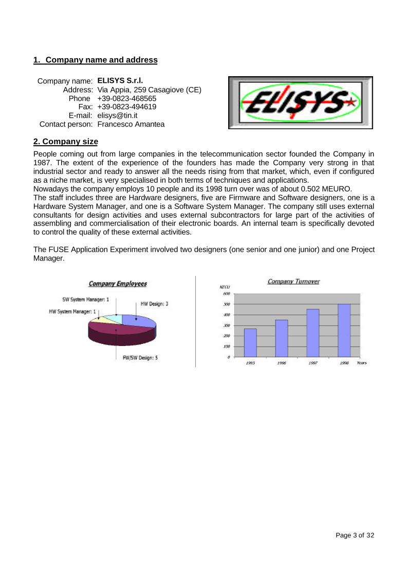
1. Company name and address
Company name: ELISYS S.r.l.Address: Via Appia, 259 Casagiove (CE)
Phone +39-0823-468565Fax: +39-0823-494619
E-mail: [email protected] person: Francesco Amantea
2. Company sizePeople coming out from large companies in the telecommunication sector founded the Company in1987. The extent of the experience of the founders has made the Company very strong in thatindustrial sector and ready to answer all the needs rising from that market, which, even if configuredas a niche market, is very specialised in both terms of techniques and applications.Nowadays the company employs 10 people and its 1998 turn over was of about 0.502 MEURO.The staff includes three are Hardware designers, five are Firmware and Software designers, one is aHardware System Manager, and one is a Software System Manager. The company still uses externalconsultants for design activities and uses external subcontractors for large part of the activities ofassembling and commercialisation of their electronic boards. An internal team is specifically devotedto control the quality of these external activities.
The FUSE Application Experiment involved two designers (one senior and one junior) and one ProjectManager.

Page 4 of 32
3. Company business description
ELYSIS Company can be classified, in accordance with the European standard classification NACE-PRODCOM within the industrial sector of Telegraph and Telephone Apparatus and Equipment andRadio and Electronic Capital Goods – PRODCOM 3220.
Main ELISYS activities are design, production and sale of Telecommunication Test Equipment,Automation Equipment, as well as design services for other companies.
Design service, which covers only 30% of the total Company’s business, is especially oriented todesign customised applications for companies involved in the Telecommunication and Automationfields.
Automation Equipment cover 10% of turnover, mainly generated by the sales of testers for the QualityFreezer-Cycle and of an Eight Sensor-Position Detection System.
Telecommunication Test Equipment is the most important ELISYS’ product line, which contributes upto half of the total Company’s revenue. These test equipment are used to test residential DECT(Digital Enhanced Cordless Telecommunication) telephone system and DECT PABX. The mainproduct within this family is DTG16/2 - the equipment that has been improved with this FUSE AE. It isused to test telephones via a telephone lines simulator, and to test telephone lines and exchanges viaa telephone simulator.
Since main ELISYS product is the Telecommunication Test Equipment, the Company is able to give adedicated post-sale support in this field to the companies requiring it.
Percentage contribution of the various activities to the total company turnover is reported hereafter. Itis referred to the year 1998.
ELISYS Turnover breakdown
5%10%
30%
5%
50%
Telecommunication Test Equiment
Other Test Equipment
Automation Equipment
Design Service
Post Sale Service and Other

Page 5 of 32
Company products
Telecommunication Test Equipment
The main product within this family is DTG16/2, used to test the DECT system. It is the product thatwas improved with the Application Experiment and its deep description is reported in sections 5 and 6.
Other products of the family are Exchange Simulator and Telephone Simulator, described below. Boththese products have been already improved using the same technology, FPGA, introduced thanks tothe AE.
• SC1 - Exchange Simulator is a product that permits to the phone-terminals manufacturers to test and qualify their products. Thesystem SC1, based on MCS-51 micro-controller, completelysubstitutes a normal Exchange by simulating 8 analoguetelephone-lines. Up to four SC1 are connectable to obtain thesimulation of 32 analogue phone lines. One PC with ELISYSgraphic application SW configures and controls all the SC1connected via serial-bus.Some typical tests performed by SC1 are:Programmable Ring Generator, Teletaxt Pulse Generator, Decade and DTMF signal recognition,Tones Generation, Voice-Switch for two or plus vocal channels. The picture shows the SC1frontpanel.
• ST1 - Telephone Simulator is a product that simulates thecomplete functionalities of 8 analogue telephones. TheST1 is based on micro-controller, and up to four ST1 canbe connected to obtain a 32 Analogue TelephoneTerminals. One PC with ELISYS graphic application SWconfigures and controls all the ST1 connected via serial-bus.Typical tests performed by ST1 are Ring Detector,Teletaxt Detector, Pulse Dialling, DTMF Tone Detector,and Tone Generation.The pictures shows the Telephone Simulator ST1 and anELISYS SW screen-out. The two different SWs managingST1 and SC1 products have very similar user interfaces.
Automation Equipment
A brief description of the main products realised by ELISYS in the field of automation is reported below:• DATALOG It is a 80C31 microprocessor-based product that is used by MERLONI Industries (one
of the main Italian manufacturers of electro-domestic appliances) as tester of the Quality Freezer-Cycle for the production line of their refrigerators. Some of DATALOG functions are: InternalFridge temperature detector, check of Power in the Time Unit (Energy Measurement with 5% ofprecision), reporting of all data to control host via serial-port.
• EC8 It detects the status of eight position-sensors. Several EC8 are connectable together viaI2Cbus serial-bus (as slaves) and to a master I2Cbus controller that polls the status of all EC8.With the EC8 blocks plus the master lots of different architectures are realisable i.e. VehiclePosition Detection systems sold to ANSALDO, one of the major Italian companies.

Page 6 of 32
4. Company markets and competitive position at the start of the AE
With more than one hundred million EURO of investments, the Italian region named Campania hasbeen becoming the Telecommunication Pole in Italy. The Telecommunication Authority resides in the county city of Napoli and in Napoli many Italian andforeign operators are pursuing many interesting projects. In the provinces of Napoli and Caserta thereare many Telecommunication companies with high level of specialisation; among these companiesthere are: IPM (leader in telephonic systems and equipment) with thousands of employees, ALCATEL,ERICSSON, and others. ELISYS is located in the centre of this pole. ELISYS history testify its experience in the market ofTelecommunication Test equipment, with the Company’s founders coming out from some of theselarge telecommunication companies. The Telecommunication Test market is characterised by:• the need of high cost test equipment, able to qualify and certificate the realised telecom products;• the need of low/medium cost test equipment, able to perform a production test.
Very large companies, namely Wandel & Goldman and Hewlett & Packard, retain the high cost sectorand share 65% of the total market of telecommunication test equipment; companies like ELISYS andNECSY retain the low/medium cost sector.NECSY, maybe main ELYSIS’ competitor, is located in the North-East of Italy and is very aggressiveand competitive on the market. ELISYS is located in the middle of the southern TelecommunicationPole: it is the only company that designs and produces Telecom Test Equipment in this pole, where itsales to some big telecom companies present there, like SIEMENS Telematica, ALCATEL,MARCONI, TELITAL (a very aggressive Italian company recently entered in the telecom market).Other companies involved in production and sales of Telecom Test Equipment are distributed in all theEU countries, especially in Germany.
At the start of this AE, ELISYS market share was of about 12 % of the domestic market, as reported inthe following chart that shows the breakdown of Italian market for all Telecommunication Test
Equipment (DECT, Phone Tester, Exchange Tester).At the beginning of 1997, two big companies manufacturing products for DECT (Digital EnhancedCordless Telecommunication) were activated by TELECOM ITALIA, major Italian telecom provider, tosupply DECT Equipment. As a matter of fact TELECOM ITALIA was planning to launch a new servicefor its customers, known as FIDO – popular dog’s name in Italy, to mean someone who faithfullyfollows you anywhere -, with which home cordless phones could have been used to receive or makephone calls through the residential lines while moving in the city area. This new service would haverequired to install lots of DECT systems in different places of all major Italian cities and towns.Companies involved in this new business were ITALTEL and ERICSSON. Since ITALTEL is one ofthe major Company’s customers as for the Telecom Test Equipment, ELISYS supplied them with the
35%
30%
12%
15%8%
Hewlett Packard
Wandel&Gold.
ELISYS
NECSY
Others
Telecom Test Equipment: Italian Market Share in '98
Page 7 of 32
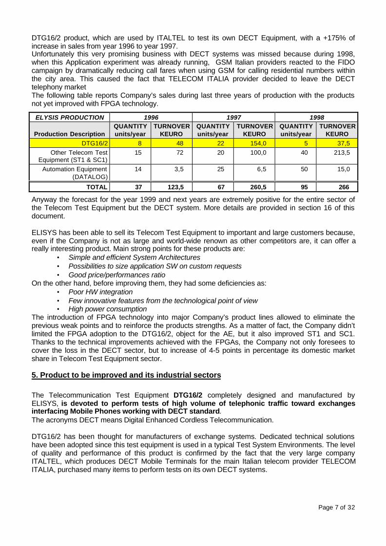
DTG16/2 product, which are used by ITALTEL to test its own DECT Equipment, with a +175% ofincrease in sales from year 1996 to year 1997.Unfortunately this very promising business with DECT systems was missed because during 1998,when this Application experiment was already running, GSM Italian providers reacted to the FIDOcampaign by dramatically reducing call fares when using GSM for calling residential numbers withinthe city area. This caused the fact that TELECOM ITALIA provider decided to leave the DECTtelephony marketThe following table reports Company’s sales during last three years of production with the productsnot yet improved with FPGA technology.
ELYSIS PRODUCTION 1996 1997 1998
Production DescriptionQUANTITYunits/year
TURNOVERKEURO
QUANTITYunits/year
TURNOVERKEURO
QUANTITYunits/year
TURNOVERKEURO
DTG16/2 8 48 22 154,0 5 37,5Other Telecom Test
Equipment (ST1 & SC1)15 72 20 100,0 40 213,5
Automation Equipment(DATALOG)
14 3,5 25 6,5 50 15,0
TOTAL 37 123,5 67 260,5 95 266
Anyway the forecast for the year 1999 and next years are extremely positive for the entire sector ofthe Telecom Test Equipment but the DECT system. More details are provided in section 16 of thisdocument.
ELISYS has been able to sell its Telecom Test Equipment to important and large customers because,even if the Company is not as large and world-wide renown as other competitors are, it can offer areally interesting product. Main strong points for these products are:
• Simple and efficient System Architectures• Possibilities to size application SW on custom requests• Good price/performances ratio
On the other hand, before improving them, they had some deficiencies as:• Poor HW integration• Few innovative features from the technological point of view• High power consumption
The introduction of FPGA technology into major Company’s product lines allowed to eliminate theprevious weak points and to reinforce the products strengths. As a matter of fact, the Company didn’tlimited the FPGA adoption to the DTG16/2, object for the AE, but it also improved ST1 and SC1.Thanks to the technical improvements achieved with the FPGAs, the Company not only foresees tocover the loss in the DECT sector, but to increase of 4-5 points in percentage its domestic marketshare in Telecom Test Equipment sector.
5. Product to be improved and its industrial sectors
The Telecommunication Test Equipment DTG16/2 completely designed and manufactured byELISYS, is devoted to perform tests of high volume of telephonic traffic toward exchangesinterfacing Mobile Phones working with DECT standard. The acronyms DECT means Digital Enhanced Cordless Telecommunication. DTG16/2 has been thought for manufacturers of exchange systems. Dedicated technical solutionshave been adopted since this test equipment is used in a typical Test System Environments. The levelof quality and performance of this product is confirmed by the fact that the very large companyITALTEL, which produces DECT Mobile Terminals for the main Italian telecom provider TELECOMITALIA, purchased many items to perform tests on its own DECT systems.

Page 8 of 32
Following a simple block diagram reports a typical scenario for DECT test:
PC runs a SW application realised by the Company allowing:
• Creation and Configuration of different test scenarios• Start Test Session• Test Monitoring• Test Reports
The SW application is connected via serial link to the test system core represented by the DTG 16/2.
DTG16/2PC
with
SW Application
DECTEXCHANGE
UNDERTEST
RS-232CoaxCable
DECT TRAFFIC GENERATOR
Page 9 of 32
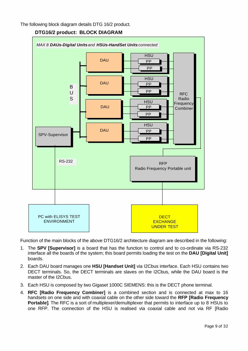
The following block diagram details DTG 16/2 product.
DTG16/2 product: BLOCK DIAGRAM
Function of the main blocks of the above DTG16/2 architecture diagram are described in the following:
1. The SPV [Supervisor] is a board that has the function to control and to co-ordinate via RS-232interface all the boards of the system; this board permits loading the test on the DAU [Digital Unit]boards.
2. Each DAU board manages one HSU [Handset Unit] via I2Cbus interface. Each HSU contains twoDECT terminals. So, the DECT terminals are slaves on the I2Cbus, while the DAU board is themaster of the I2Cbus.
3. Each HSU is composed by two Gigaset 1000C SIEMENS: this is the DECT phone terminal.
4. RFC [Radio Frequency Combiner] is a combined section and is connected at max to 16handsets on one side and with coaxial cable on the other side toward the RFP [Radio FrequencyPortable]. The RFC is a sort of multiplexer/demultiplexer that permits to interface up to 8 HSUs toone RFP. The connection of the HSU is realised via coaxial cable and not via RF [Radio
MAX 8 DAUs-Digital Units and HSUs-HandSet Units connected
DAUHSUPP
PP
DAU
DAU
DAU
HSU
HSU
HSU
PP
PP
PP
PP
PP
PP
RFCRadio
FrequencyCombiner
RFPRadio Frequency Portable unit
PC with ELISYS TESTENVIRONMENT
DECTEXCHANGE
UNDER TEST
SPV-Supervisor
BUS
RS-232

Page 10 of 32
Frequency] for minimising the possible interference in Test Environment where a lot of DECTTerminals are present.
5. The RFP is a base radio DECTalk and is connected to DECT Exchange under test and to RFC viacoaxial cable.
Then, with DTG16/2 and the SW on PC it is possible to build Test Sessions. All the DAU boards, co-ordinated by the SPV, can run in sequential mode a test series to simulate the DECT attaches incentral exchange to verify, in a stressed mode, the correct running. The most rEUROrrent board inthe described system is the Digital Unit-DAU.
Following we reported the DAU block diagram:
The DAU board is composed by:• micro-controller part section: 80C31 micro-P and a ROM-FLASH block that contain the FW and
the configurable data of the DAU board;• Digital part: RAM 32kbytes chip (only 128 used for DAU), Watch-Dog Controller, I2Cbus
Controller, Glue Logic and I/O Register. The Digital part before described is very common to all boards based on microprocessors. Within theexisting product it was realised with traditional discrete components of SSI and MSI technology, as74XX series. In particular, this Digital Part was composed by 35 components of 74hcxxx series, 1I2CBUS Controller, and 1 RAM chip 62256.
In the DTG16/2 product it is possible to plug in two different accessory boards, which allow to test theDECT systems in particular applications. These boards are named:
• POTS, that simulates a traditional DECT - To - Analogue Phone network
80C31
ROMand
FLASH
I2CBUS TO DECT TELEPHONE
SWITCH, TONEDETECT ANDGENERATION
RAM
I2CBUSController
REGISTER DECODERS ANDGLUE LOGIC 74HCXXX x 35
ADDRESS
DATA
DIGITAL PART: I/O Register, Watch-Dog,I2Cbus and Glue Logic
Watch DogController
Digital Unit-DAU: BLOCK DIAGRAM

Page 11 of 32
• ISDN, that simulates a DECT - To - ISDN network
The architectures of these boards are similar to DAU. In fact both the micro-controller part and theDigital part are the same of the DAU board, while the specific functions have been added to realise therequired functions. Since the DAU boards are replicated inside the DTG16/2 product, all the DAU weaknesses aremultiplied for the number of all DAU present. Even if from the technical point of view, all the HWfunctionalities realised using the traditional discrete digital components match the functions required,from the economical point of view, this technology is very expensive with respect to microelectronicsolutions like FPGA technology.Main problems rising from the DAU discrete components part can be classified into two main areas:technical and economical.
Technical drawbacks• Very high assembling time, due to
the long part list of discretecomponents to be used
• Test too long• Low board reliability• Large size of Printed Board• High power consumption
Economical drawbacks• High manufacturing costs due to
purchasing of so many components,as well as to assembling and test ofthe DAU boards.
• High cost to manage and to stock somany components
These drawbacks were the basis that convinced ELISYS to search a new technological solution forthe DAU board and especially for the Digital part of it.
6. Description of the technical product improvements
As previously described, the cost for the DAU boards has a negative economic impact on theDTG16/2 product overall cost. This is mostly due to the presence of a high number of traditionaldiscrete components and this negative effect is as much heavy as higher the number of DAU boardsis, up to a maximum of 8 DAU boards per each DTG16/2. The project goal was hence that of overcoming DAU weak-points, here shortly summarised:As far as costs are concerned:1. High assembling costs2. High test costs3. High number items in the DAU bill of materials and high warehouse costs
As far as product performance:1. Large size of Printed Board2. High power consumption3. Product reliability could be improved
With the realised AE all DAU boards were replaced with a smarter, general purpose board, co-processing like, that thanks to the benefits allowed by FPGA technology could improve the existingDTG16/2 test equipment as for manufacturing costs and performance.
Old DAU Board

Page 12 of 32
Its general purpose functionality makes it easily reusable in other ELISYS products, improving themtoo.
The following block diagram shows the new DAU architecture, where the old Digital Part (please referto the block diagram on the previous paragraph) has been replaced by the DECT TESTER FPGA.
The realised DECT TESTER FPGA has the same functionality carried out by the discrete componentsof the old DAU Digital Part. Next page shows the block diagram of realised DECT TESTER FPGA.
80C31
ROM andFLASH
SWITCH, TONEDETECT ANDGENERATIONADDRESS
DATA
I2CBUS
DAU BLOCK DIAGRAM: New Architecture with FPGA
DECT TESTER FPGA

Page 13 of 32
DECT TESTER FPGA: BLOCK DIAGRAM
PA0-PA7 SCL SDL PB0-PB7 PC0-PC7 PD0-PD7
SEL A SEL B SEL C SEL D
D0:D7
A0:A7
RESETOUT S0 RESETIN S1
MCLK
ALE CSPN RDN WRN INT
AD0:AD7 A8:A19
In the DECT TESTER block diagram we note the following blocks:
• MP- ITF is a microprocessor interface, a block that permits the interaction with the externalMCS-51 microprocessor by addressing each internal block and by performing read/write forRAM block, I/O ports and internal service registers.
• I2Cbus Controller to realise the relative standard sequence, protocol, arbitration and timing ofthe I2Cbus serial bus standard. This block will use the mP interface to communicate bi-directionally with the external microprocessor. It uses the standard I2Cbus signal toward theexternal: SDA and SCL.
• RAM Block with 256 bytes available to be used in all applications requiring less then 256 bytes(DAU uses only 128 bytes). The use of standard RAM chip is avoided.
• Watch Dog Timer or Timer is the block that, opportunely programmed, realises a standardwatch-dog timer or a standard normal timer function.
• 4 x I/O Ports blocks are usable as a sort of I/O Port expander of the microprocessor. In addition,when opportunely programmed by the microprocessor, it is possible to configure a certainnumber of I/O pins as a chip-select function.
The device used to realise DECT TESTER is a 10K20 ALTERA FPGA. The package used is 144 pinsTQFP. The used pins are 89 (60 signals + 29 Power supply), meaning 62 % of the total. The internalused gates are about the 70 %. 30% spare space is still available inside the FPGA for future productenhancements. The usability of remaining space is strongly dependent on the efficiency of the
mP-ITF BT
256 BYTESRAM
I/OPORT A0:A7
I/OPORT B0:B7
I/OPORT C0:C7
I/OPORT D0:D7
I2C BUSCONTROLLER
WATCH DOGTIMER OR TIMER
Page 14 of 32
adopted FPGA design methodology, in the sense that the device functionality achieved and the non-used gates are in a relationship of non linearity, based upon the type of design made. In this case over50 % of the functionalities were implemented by using the VHDL language.
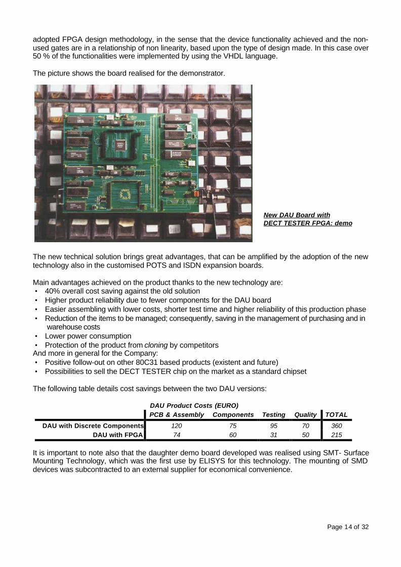
The picture shows the board realised for the demonstrator.
The new technical solution brings great advantages, that can be amplified by the adoption of the newtechnology also in the customised POTS and ISDN expansion boards.
Main advantages achieved on the product thanks to the new technology are:• 40% overall cost saving against the old solution• Higher product reliability due to fewer components for the DAU board• Easier assembling with lower costs, shorter test time and higher reliability of this production phase• Reduction of the items to be managed; consequently, saving in the management of purchasing and in
warehouse costs• Lower power consumption• Protection of the product from cloning by competitorsAnd more in general for the Company:• Positive follow-out on other 80C31 based products (existent and future)• Possibilities to sell the DECT TESTER chip on the market as a standard chipset
The following table details cost savings between the two DAU versions:
It is important to note also that the daughter demo board developed was realised using SMT- SurfaceMounting Technology, which was the first use by ELISYS for this technology. The mounting of SMDdevices was subcontracted to an external supplier for economical convenience.
New DAU Board withDECT TESTER FPGA: demo
DAU Product Costs (EURO)PCB & Assembly Components Testing Quality TOTAL
DAU with Discrete Components 120 75 95 70 360DAU with FPGA 74 60 31 50 215
Page 15 of 32
7. Choices and rationale for the selected technologies, tools and methodologiesOne of the most important phases in the design of this project was the choice of the technology toadopt, and once chosen, the research for development tools and the definition of workmethodologies.
The first step was to identify the possible applicable technology. The following three differenttechnologies were considered as options for carrying out the product technological improvement:
• Micro-controller & Discrete Component• FPGA• ASIC
The first one represented the same technological solution already adopted in the old product, basedon a microcontroller with discrete components. Although the entire product could be redesigned usinga better architecture, then assuring better performance, practically all the weak points of the oldproduct would remain unchanged in the new one.The second and the third options represent very innovative technologies for the Company.
ELISYS, jointly with the TTN, took into account all the three most suitable technologies, considering asselection criteria:
• The required level of integration to be obtained• The target cost for the new module, on a typical production volume (200/300 pcs/year)• Related risks• Time-to-market
The table here below summarises the result of the analysis carried out, in accordance with the selection criteriaadopted:
Issues Discrete logic FPGA solution ASIC solutionIntegration density Low (components dimensions
and number is relevant)Good (integration willincrease in future)
Very Good
Device cost Medium Very Good Very HighRisks Iteration could be required,
although at low costno risk (re-programmabledevice, modify possibilities)
Iteration could berequired at high cost
Time to Market Weeks Hours-Weeks Months
The yearly production volume was considered as 12 new boards x 25 DGT16/2 = 300 pcs/year.
ASIC technology was reputed not convenient: although the relative cost per gate be lower in a ASICthan with an FPGA. In fact the Non-Recurrent Engineering costs required by ASICs are so high thatthe Company production should absorb up to 5.000 pieces per year to have a reasonable spread ofthose costs over the production volume. Moreover, the time to market is weeks for the FPGA solutionversus months for the ASIC one. The risk is very high in ASIC, too.
Finally it was decided to improve the product by choosing between FPGA and DISCRETE LOGIC.The use of components with discrete logic was eliminated because this technology did not allow theCompany to achieve the goals fixed for costs and integration. The required performance could havebeen got through discrete logic only by increasing the number of cards used in DGT16/2 of two units,thus increasing costs out of target. Furthermore the increased diffusion of programmable devices atincreasingly affordable prices tipped the balance in favour of this new technology.In particular it is worthy to mention the results of the Company analysis on the two technologies,FPGA and DISCRETE LOGIC, highlighting their main differences:1. the use of FPGA technology could bring to a reduction of the PCB area of about 50%.2. the cost for assembly and testing an FPGA-based board would be 25-30% less than the cost for
carrying out the same activities with a board using discrete logic.

Page 16 of 32
3. FPGA offers a high flexibility level: different functions can be accommodated on board accordingwith different applications
4. FPGA offers a better design control by means of simulation tools5. FPGA offers a reduced development time and risks, thanks to the on board programmability and
test iteration6. FPGA represents a flexible solution thereby reducing the time to market, which can be considered
from hours to weeks.7. FPGA offers a foreseen price reduction due to technology fast spread on the market and increases
in manufactured volumes.8. FPGA offers a high level of replication on all other ELISYS products.
COMPONENTS AND DEVELOPMENT TOOLS:
Another important stage was the choice of FPGA type to be adopted and the relative developmenttools. With regards to the development tools, ALTERA and XILINX tools were compared. Anevaluation from an economical standpoint had shown few differences. From a technical point of view,ALTERA tool was considered to be easier to use, with extremely reduced compilation times, and asimulation tool that is particularly effective even in the introduction of test vectors. Furthermore,according to the Company’s evaluations, the technological progress of the ALTERA tool will lead tothe development of components with an increasing number of gates, thereby reducing the use ofspace to minor costs. For all of these reasons it was decided to use ALTERA components andALTERA development tools.
DESIGN METHODOLOGIES:
The Company decided to use a design methodology, which could be appropriate for the FPGA projectbut also for an eventual future design migration towards ASICs, in case production volume could allowto afford this technology. The Company designed with an EDA development environment, basing onthe usage of: VHDL language for the functional circuit description, HW Logic Synthesiser, GraphicEditor, Logic Simulator, and Fitter.
One of the main reasons for the choice of a VDHL method of design for FPGA was due to the will ofthe Company to acquire a powerful HW design method, suitable also for easily retargeting the FPGAproject into an ASIC one.
8. Expertise and experience in microelectronics of the company and the staff allocated to theproject
Since its establishment, ELISYS designed PCBs based on traditional discrete logic (74HCxxx family)and on micro-controller; the company got wide experience in the application of the MCS-51 Intelmicro-controller family, especially for Telecom and Automation real time applications.The company also developed and still uses a proprietary real time multitasking operative systemtailored for the Company typical system application: Telecommunication Test Equipment.ELISYS is also experienced in a lot in Telecommunication standards, protocols and technologies as:PCM (Pulse Code Modulation), X75, HDSL (High-speed Digital Subscriber Loop), ADSL (AsymmetricDigital Subscriber Loop), ISDN (Integrated Services Digital Network), DECT (Digital EnhancedCordless Telecommunication), etc.
The HW designs realised before this AE experience had followed the traditional approach. The onlyEDA tools present in ELISYS before the AE were a Graphic Editor to realise the schematic-capture ofHW designs and a SW to realise printed board layout. This operational habit generated HW design"Obsolete at Start".Even project management activity had not ever been properly defined, because there had ever beenthe need neither to control or co-ordinate the activities of subcontractors, nor to make human andeconomical resources available within fixed time frame or mode.

Page 17 of 32
The company structure includes a HW department and a SW department and relative managers withtechnical responsibilities. HW department counts 3 design engineers, SW department counts 5 designengineers. The company is also supported by a certain number of external consultants when thecompany has job peaks.
One Project Manager and two designers were assigned to the AE project: 1 Technical Manager(Senior Designer) and 1 HW Designer (Senior Designer) who, at the start of the project, did not haveany previous experience with programmable logic, EDA development tools, or VHDL language.
9. Workplan and rationale
The introduction of a new technology, with the risks that the process might have, combined with theneed to respect design and production timetables, required the preparation of a detailed work plan inaccordance with the rules of project management.
The workplan was divided into 5 work packages:1. Management2. Training3. Design4. Prototype and Testing5. Dissemination
Activities were carried out by ELISYS, having responsibility for the project. The Company enjoyed thesupport of one qualified subcontractor, CESVIT MICROELETTRONICA Srl, responsible for knowledgetransfer to the Company on the new FPGA technology and tools.
Each workpackage is detailed in the following, showing which were objective, measures of successand deliverables for activities carried out.The plan also shows in detail roles and responsibility for the staff that was involved in the project, bothfrom the Company and from the subcontractor.Tables summarise for each workpackage breakdown of efforts and sustained costs.
ManagementELISYS had the responsibility of the project control. The Company has then co-ordinated,supervised and controlled all the necessary activities. The Company spent in this task 120personhours.
TrainingThe goal for the training activities was to acquire the necessary technical and managerial know-how, in order to achieve the project success and to apply autonomously the FPGA technology onother Company products. This task took place in three different phases. The first one was aboutbasics for the VHDL language, to be used to describe at HW level the functional components. Thesecond training phase was about the application of VHDL language to MAXPLUS2 by ALTERAEDA Tools and the specific FPGA device chosen. The third training phase was about the VHDLdescription, the simulation, and the synthesis of the PARTNER 51, the FUSE AE project. TheCompany effort in this workpackage was 220 personhours; the subcontractor effort was 80personhours.
DesignThe design goal was to transform the DECT TESTER specifications in a correctly running FPGAdevice. In the first task, the functional specification was deeply analysed end then stated in adefinitive way. With the second task, all the stated functional specification was translated in aVHDL circuit description, simulating all the single blocks that compose the entire FPGA. All theblocks interconnected each others were simulated, too. This was done in order to check thecorrectness of the FPGA functionalities in front of the stated specification. The Company spent inthis workpackage 584 personhours; the subcontractor effort was 102 personhours.
Prototyping and Testing

Page 18 of 32
A prototype was realised in order to verify the real working of PARTNER 51 against initialspecification. The breadboard containing the FPGA was realised. The tests were realised viafirmware, and some little bugs were found related to the FPGA functionality. One single cycle ofreworking succeeded in solving all the problems encountered. The subcontractor helped theCompany with both test strategy definition activity and bugs search and solution. On thisworkpackage, the Company spent 128 personhours, the subcontractor 8 personhours.
Dissemination
The Company has actively spread the results reached with the Application Experiment. It hasideated and created information materials about the ELISYS AE experience and specifically aboutDECT TESTER chip. The Company was involved in this task for 80 personhours.
Following there is reported a table summarising the efforts and costs sustained by the Companyduring the DECT TESTER development by each workpackage, compared with those that wereplanned before the AE start.
The AE was carried out substantially within budgeted efforts and costs, with he very minor deviation ofless than 1%. Resources having higher labour costs were involved during the on job training had forthe design activity and those higher labour costs were compensated by a decrease in expenditures forHW and SW.
Project time schedule
First User Subcontractor
Work PackagesLabour(pdays)
Labour(KEURO)
Labour(pdays)
Labour(KEURO)
HW & SWEDA Tools(KEURO)
TOTAL(KEURO)
plan act plan act plan act plan act plan act plan act
WP 1 Management 15 15 3,00 3,00 3,00 3,00
WP 2 Training 27,5 27,5 5,50 5,50 10 10 4,86 4,86 0,5 0 10,86 10,36
WP 3 Design 73 73 14,60 16,71 12,75 12,75 6,24 6,24 1,5 0,40 22,34 23,35
WP 4 Prototyping &Testing
16 16 3,20 3,20 1 1 0,48 0,44 0,5 0 4,18 3,64
WP 5 Dissemination 10 10 2,03 2,03 2,03 2,03
TOTAL 141,5 141,5 28,33 30,44 23,75 23,75 11,58 11,54 2,5 0,40 42,41 42,38
Plan Actual WEEKS
WORKPACKAGES & TASKS 01
02
03
04
05
06
07
08
09
10
11
12
13
14
15
16
17
18
19
20
21
22
23
24
WP1. ManagementWP2. Training
Task 2.1 VHDL trainingTask 2.2 EDA ToolsTask 2.3 On Job Training
WP 3. DesignTask 3.1 SpecificationTask 3.2 Design & Logic Simulation
WP4. Prototyping and TestingTask 4.1 Prototype Board realisationTask 4.2 Testing
WP 5. Dissemination

Page 19 of 32
The initial workplan has been substantially respected, too. There were only few differences about thetraining and the testing phases:• The training about the methods of FPGA design last less long then expected for the following
reasons:• Great experience of subcontractor CESVIT in know-how transferring• ELISYS engineers very receptive• ALTERA system powerful and easy to use
• The workpackage Prototyping & Test last little bit longer then expected. In fact, the Companydecided to realise the new board with FPGA using the SMT technology. This was the first time thatthe Company used such a technology, so it required greater care to the Company for searchingcomponents, never used before, and co-ordinating PCB suppliers and components suppliers aswell as for taking care of the PCB design and SMD mounting. Additional time was spent to carry outthese extra tasks; the Company covered all the extra expenses.
The Company was quite able in catching time up and completing the work within the scheduled 6months but a project duration of one month more, even with the same number of person hours, wouldhave allowed an easier management of these unexpected deviations.
10. Subcontractor information
In order to acquire skills on the new technology, the company selected one subcontractor, whichguaranteed a fast learning process on the new design techniques and reduced the risks of projectfailure. The subcontractor was qualified to provide assistance to the company in its first design with anew technology and it fully supported ELISYS even with availability of their own facilities (i.e. state ofart tools).Thanks to the training received from subcontractor, ELISYS improved its own design capacity andclosed the existing gap between the technology level of the new products and the existing internaldesign methodologies and technologies.
The subcontractor was selected following these criteria:
- Previous experiences and technical capabilities with FPGA design- High design experience in the specific sector, software design expertise and availability of tools- An average cost less than 60 EURO/Hour
The subcontractor selected by the company was CESVIT, micro-electronics centre based in Florence,recognised by the CEC for technology transfer activities as well as by ALTERA as the Italian OfficialTraining Centre. Being a TTN, CESVIT gave also additional guarantee of commitment to theachievement of positive project results.CESVIT curriculum left no doubt about its capabilities concerning the adequacy of the technologicaltransfer required by the Company. At CESVIT headquarters the Company staff assigned to the projectwas able to enter into the world of FPGA and learn the VHDL language in a short period of time withexcellent results from the word go. The training given for project management activities was also veryimportant.
Subcontractor
Name: CESVIT S.p.a. - Microelectronics Centre
Size: 36
Business: High technology agency
Relevant expertise & experience and service provided: CESVIT S.p.a. - Microelectronics Centre gaveevidence of being able to provide services in prototype design, fabrication and test of digital systemand of board with CPLD/FPGA devices. The subcontractor had been developing CPLD/FPGA projectsfor more than 10 years.
Page 20 of 32
Moreover it is qualified to provide training and assistance to companies who do their first design usinga new technology and the Centre’s facilities, competencies as well as state of art tools, are availableto companies. The centre has a strong experience in PCB, FPGA and ASIC design and actually iscarrying out several training courses on related topics.The subcontractor demonstrated to have a lot of links with different suppliers and distributors in Italyand Europe. This was a feature that ELISYS reputed really useful to develop its project: in fact theCompany had view on components and tools of the main different vendors and also strengthened itslinks with the local distributors.In addition the selected ALTERA product line made of CESVIT the ideal candidate for the training andknow how transfer of the FPGA technology since it is a centre qualified by ALTERA for consulting andtraining on their FPGA devices and the related CAD tools.Technical support that CESVIT provided as subcontractor was about the choice of the final FPGAdevices, the VHDL basic training and FPGA design on-job training.As subcontractor CESVIT supported the Company in four different phases of the project.• it provided the know-how to set out a FPGA project; this included training on design
methodologies, and basic training on VHDL during which technical manager and designer of theCompany acquired knowledge to autonomously design the prototype.
• during the second phase, CESVIT senior engineer, ELISYS technical manager and designerestablished the functions to be integrated inside FPGA.
• during the third phase CESVIT provided training to test the feature of the FPGA device. Thistraining was carried out until ELISYS technicians had acquired the sufficient knowledge to carryout it autonomously.
• during the fourth phase CESVIT assisted ELISYS to test the DECT TESTER prototype and thedeveloped demo-board.
Personnel allocated by the Subcontractor to the AE:2 Senior Engineers1 Marketing and business analyst
Contract and compliance: ELISYS implemented a project using FPGA technology and thesubcontractor role was mainly devoted to provide training to the Company. There were no particularaspects to cover for what concerns IP either. The contract was therefore a simple one based on astandard offer describing the cost and time allocated to the work and then on the respective order.This kind of contract has demonstrated its effectiveness and adequacy with respect to the projectcharacteristics.CESVIT carried out activities within time and costs as reported in the offer/order, both relating with thetechnical and managerial aspect of the project.
11. Barriers perceived by the company in the first use of AE technology
FUSE initiative gave to ELISYS the possibility to introduce microelectronic technology in its TelecomTest Equipment products and - actually and finally - the word “Technological Innovation” isn'tconsidered anymore a chimera accessible only to large companies.Before the realisation of this AE, some of ELISYS’ employees, from time to time, had done some timidapproach to the evaluation of the opportunity to introduce technological innovations into the company(the writer, Company’s Technical Manager and Senior Designer, was one of the unlucky actor of thesetrials in the past) but punctually each trial failed, ending up to some conclusions like these:
• "The resources, in this moment, are saturated! "• " All the company's resources must be allocated on jobs immediately productive"• " The company can't support the necessary financial investment to permit the innovation! "• " This innovation could be at high-risk and in the end we could not have the desired results! "• " Our Technical Engineers don't have the right skills to enterprise a project with New Technologies!
" (Which is the right skill to learn New Technologies and consequently elevate the same skill?)• " Is this New Technology effectively innovative and will it produce the hoped cost-reduction? "
Page 21 of 32
These and other similar considerations I received in the past when I tried to introduce innovation inELISYS. When we heard about the FUSE initiative and the opportunity to rely on the free help of aTechnology Transfer Node to guide us in having more and clearer information about the newmicroelectronic technologies, I thought to have finally a powerful tool to shoot down the Company’sstrongly consolidated barriers against technological innovation.
Cultural and Managerial BarriersCultural barriers were mainly due to the Company’s policy. As many SMEs, ELISYS had always beenthinking that only big companies could have been able to employ key resources in the development ofnew projects, because only them could have faced the financial risks that this operation could involve.Therefore the Company had always preferred to employ its resources in an immediately productiveway, even knowing very well that, while doing like this, it resigned all the advantages that could havecome out from future greater developments.Another cultural barrier encountered was the absolute lack of any structured project managementmethodology, which caused the Company’s incapability to plan adequately the activities necessary todevelop such innovative projects.
Financial BarriersStarting from the Company’s point of view that it had before the Application Experiment, it is obviousthat the Company didn’t want to employ key resources either in long-term or mid-term projects ofinnovation. This was always regarded as a high financial risk, diverting resources from activitiespromptly remunerative. Another significant financial obstacle encountered was the Company’sincapability to correctly estimate the needed investments, which were reputes as high as the Companyconcluded that, even in case of success, the results didn’t justified the investments.
Technological BarriersAgain, because of its small size, ELISYS didn’t have enough knowledge to develop autonomously theproject: the only information that the technical staff had, about FPGA-based solutions, came fromElectronics Magazines and FPGA vendors. The technicians hadn’t the necessary competence toselect the best help available, either. Therefore, the risk of not being able to reach the necessaryknowledge to manage the new technology increased considerably with the risk to turn to a help notenough competent and expert.
12. Steps taken to overcome the barriers and arrive at an improved product
Cultural and Managerial barriersThe first important step taken by the company was to understand whether a small company, with alimited production of pieces/year, and a small available work force could expect to introduce newtechnologies within the company.Through the dissemination activities carried out by ENEA in Salerno University, the Company wasinformed about FUSE and it took part in a FUSE seminar organised by the local TTN.As follow up of this seminar the Company participated in a one-to-one meeting with the TTN staff andthere it had the occasion to analyse data regarding other innovative projects which had beensupported before as well as the experiences of other SMEs. This analysis fostered the belief that theCompany had the suitable characteristics for facing a project of technology innovation. One of the firstimportant steps was therefore the decision to start participating in the seminars dedicated toprogrammable logic organised by leading vendors, as well as to have other (three, before starting withthe FUSE proposal) one-to-one meetings with the TTN.During these meetings time and human resources required by the project were assessed. Due to thelack of any previous experience of the Company, its collaboration with the TTN helped to define, evenat a preliminary examination of the project, the expected project duration - no more than six months -and the work force to be allocated to the project, as well as to assess if it would have been reasonablyavailable within ELISYS resources. In this case the possibility of collaborating with a highly specialisedcentre was fundamental, since the initial project feasibility study.
Page 22 of 32
With the occasion of the FUSE proposal drawing, it was necessary also to learn to define a detailedwork plan, which foresaw the division of responsibilities, as well as detailed project controls againstfixed measures of success, through activities of periodical reporting. This forced the Company toshare both economical and human resources also with this new project and to find out the way to runthe Application Experiment in parallel with the usual Company’s activities.This planning methodology had never been carried out within the company, and in the end, thanks tothe help of the TTN, it was easily achieved.
Financial barriersSurpassing the financial barriers meant making a precise estimate of the necessary investments. Itwas calculated that the project needed an investment of approximately 40 KEURO, with a pay-backperiod of approximately one years and half.The quantification of the investments, done together the TTN, produced figures lower than whatexpected by the Company. The needed effort was reputed acceptable and completely in-line with theAE to be realised.
Technical barriersIn order to overcome the obstacles of a technological nature, it was considered necessary to consultagain the TTN.Its advice helped consistently especially because:• it was a super-parts presence, not linked to any commercial vendor, and it revealed objective in
presenting the possibilities and the potentialities of microelectronics and, more in particular, ofFPGA technology;
• it showed a good experience in training people on technical matters, presenting possible problemsand related workarounds. The Company appreciated mostly its capacity to involve to makeevolved ELISYS designers and managers in innovative technologies and in their handling.
Company barriers to introduce new technology: who helped how
CulturalBarriers
CESVIT as TTN
Dissemination ofresults achieved by
other SMEsProject feasibility study
FinancialBarriers
CESVIT as TTN
Realisticestimate of theinvestment and
its pay-backperiod
TechnologicalBarriers
CESVIT as TTNProject management training
CESVIT as subcontractorTraining on:
• VHDL basics• ALTERA TOOLS• DEMO-BOARD TEST
with a Daughter-Boardwith SMT layout (the firsttime for ELISYS)
On job training during thedesign phase
DECT TESTER
FPGA based, chipset for MCS-51micro-controller;
Telecom Test EquipmentApplication
4 x 8 bits digital I/O PORTs1 Programmable TIMER
1 I2Cbus Controller1 x 256 RAM Block

Page 23 of 32
13. Knowledge and experience acquired
This project has allowed the company to acquire skills and know-how not only for the application ofmicroelectronics technology, but also for project management, documenting and reporting activities.Before participating in the FUSE program, the company of course proceeded with the issuing of aspecification for the realisation of a new project, but it had never felt the need to define a detailed workplan and resources assignment (human and tools). Participation in the FUSE program required thecompany to define a work plan; they were forced to respect a timetable and this caused the companyto undertake, for the first time, an actual management of a project.It was also the first time that a detailed analysis of the market for the new product and the calculationof its estimated production costs in comparison with those of the old product were put into effect.In other words ELISYS has got now some people with stronger capability in "technical & managerial"estimation and in problem-solving in the complex and competitive world of electronic design andproduction, but most of all it has got people with stronger capability of "looking ahead ".From the point of view of the enterprise-system, today ELISYS is a more sensitive company and ablerto follow the technical innovation. An enormous added-value returned to the company from the AEexperience in terms of job organisation and planning capability.It may be said without any doubt, that, apart from the advantages that the improved new products mayoffer, this fact alone may be considered as a valuable and extremely positive result.
Obviously the introduction of FPGA technology has considerably increased the technical knowledge ofall the staff involved in the project, with the acquisition of new design methodologies and of solutionsto problems related to those methodologies. In details the company learned about:• Criteria for choosing FPGA components to be used, considering the aspects of economics,
availability of components, problems related to the gate-numbering and assembly techniques andrelevant solutions.
• FPGA device specification• VHDL description and synthesis of the project.• Methods for he implementation of complex functionality like that of the I2Cbus block contained
within DECT TESTER• ALTERA development environment• Definition of test vectors and project simulation.• Problem solving related to FPGA programming on-board• SMT techniques as for the Daughter-Board realisation (DEMO-BOARD development)
To the list reported above we must add the fact that from the few problems encountered and from thedelays accumulated during the project execution, which were mainly due to external manufacturers,the Company learned how to manage the start-up stages of a new product manufacture.
14. Lessons learnt
Apart from the technical experience, we can here shortly summarised which were the main,unexpected achievements the Company realised during or at the end of the Application Experiment:
1. When the technological innovation is really worthy, the Company can benefit from it even ifunforeseeable market changes occur and this causes a product being phased out and the newtechnology being used in other products
We believe this is the main lesson that this AE can offer to other companies guessing to adopt newmicroelectronic technologies
2. Your Company always learns, but significant and faster step-aheads can be done only with thesupport of suitable consulting firms

Page 24 of 32
One of the most important factors in a new project success is the choice of consultants. This choice isas much important as using a new technology for the first time. In this case, the subcontractor canintroduce the company to the new technology rapidly and without causing trouble to the company'sday by day activities.
For example, during the initial stages of the use of the new development tools, the support receivedvia telephone by the subcontractor CESVIT was extremely important. They were able to offer animmediate solution to a risen problem thus avoiding the Company loosing too much time orinterrupting other activities to let other resources working on the problem. This aspect is particularlyimportant when a new project is realised in addition to the company’s normal activities, as it alwaysoccur in small companies where time efficiency is crucial.
3. Little reworking is necessary when the design phase has been properly carried out
The test phase should be regarded as the possibility to widen and improve the comprehension of thedimensions of the design problems as well as the check-point for the adequacy of the solutions madeduring the design stages, rather then a simple check on the product functionality. In our design fewmodifications were necessary on the prototype to pass the required tests.
This was due to the main following, winning points:
Correct specification - The first request made to the company by sub-contractor was to supply anexhaustive specification, both at product level - clear ideas of the characteristics of the new product –and at system level for the new DAU board, object of the innovation. Only at a second step thecompany was requested for detailed specification of the HW subset to be integrated into the FPGA.While general specification were quite easily issued by the Company, some more difficulties were withthe specification of the FPGA component. For this task the sub-contractor helped the company, as it did not have any previous experience. Thespecification was resolved with a description of the I2CBus characteristics, a description of the partrelative to internal timer, a description of the bi-directional general purpose I/O Port and an indicationof the discrete components used (glue-logic). Before that this specification were drawn up, the Company did not have a precise idea of the numberof gates available within the various FPGA component sizes, or of their relative cost. An initial analysiscarried out by the company designers and the subcontractor immediately showed that the entireproject could not fit into a FPGA chip PTH (Pin Through Hole): it was necessary to use a PQFP(Plastic Quad Flat Package) with a minimum number of 144 pins. This constraint forced ELISYS to look for some solutions in order to mount this package type (SMDtechnology), since this kind of mounting technology wasn't present in ELISYS at that time. Thesolution was found in isolating the FPGA component on a sort of daughter-board and only the latterwas mounted SMT by a specialised external company.The correct specification avoided that the Company should come later to problems like designretargeting on FPGA devices of larger sizes or should face the unexpected problem of using SMT.
A prompt project analysis therefore brought about an immediate modification of the preliminaryspecification. This type of analysis was extremely important for the project. It was carried out in arelatively short time: with the help of subcontractor, based on the specification for device occupation interms of gates, it was possible to make a decision on the right components to use and thedevelopment tools necessary for their programming.
Training and investments in resources – training the staff on the new technology and on VHDL was, inthe light of the results, undoubtedly important for the successful realisation of the project.
4. Choosing the right design methodology can better the design efficiency
Within the developed DECT TESTER FPGA 30% of the space left out, available for future productsenhancements. The usability of remaining space is strongly dependent on the efficiency of theadopted FPGA design methodology, in the sense that the device functionality achieved and the non-used gates are in a relationship of non linearity, based upon the type of design made. In this case over50 % of the functionality were implemented by using the VHDL language.

Page 25 of 32
It has to be noted that it was not possible to achieve the required characteristics using a completelyVHDL synthesis, and that the use of ALTERA library components was necessary. VHDL revealed a very good tool for state-machine realisation, which were mostly present in theI2Cbusblock.
15. Resulting product, its industrialisation and internal replication
The Company had a strong interest in industrialising the DECT TESTER prototype, since it can beregarded as a sort of chip-set that can drastically reduce the manufacturing cost of a large number ofELISYS products, also covering different applications and sectors. Industrialisation and internal replication in Telecom Test Equipment sector TELECOM ITALIA decided to leave DECT telephony market, due to the big new competition causedby the Managers of GSM service in Italy (Omnitel and TIM companies) with a low price policy for thecity-market telephony. After an update during 1998 of the market analysis carried out before thestarting of the AE, due to this unpredictable DECT market contraction, and after a more realisticestimation of the 1999 and 2000 expected sales, ELISYS decided that, for the inevitable decrease ofDTG16/2 market it wasn't convenient applying DECT TESTER to the DTG16/2, redesigning a newDAU board. Even if the Company lowered the stress on the DTG16/2 it didn’t decided to discontinue it completelyand the Company is now investigating the possibility to contact DECT equipment manufacturers inGermany, offering the improved DTG16/2 product to that market, which didn’t suffered of the lackcaused in Italy by external sources. ELISYS decided to industrialise the DECT TESTER anyway, since this revealed to be profitable alsofor the other lines of products in the Telecom Test Equipment sector, which showed a good salestrend. These products are:
- ST1: Telephone Simulator- SC1: Exchange Simulator
A great deal is expected due to these new improved products, above all thanks to the increase incompetitiveness against the other Telecom Test Equipment manufacturers. Time to market, from therealisation of the prototype for the first new products (SC1: Exchange Simulator and ST1: TelephoneSimulator) - with DECT TESTER on board - up to the commercialisation of the final products, isenvisaged in 5 months approximately.
Industrialisation and internal replication in Automation Test EquipmentOne product within the product line for automation applications - named DATALOG (described insection 3) - has and will have for the next years to come a good sales-trend and ELISYS decided toapply, as an internal FUSE replication, DECT TESTER chip on it, thus reducing its cost. This costreduction will generate an increase of the Company’s market share in the specific market sector.
The estimate possibilities of using DECT TESTER chip will require a production volume of 150/200pieces for the new units starting in June 1999.

Page 26 of 32
The following table details the specific activities required for industrialisation for the PCB mounting theDECT TESTER module. Any other additional activity specific to the product target for innovation (ST1,SC1 or DATALOG) was separately charged.
DECT TESTER industrialisationweeks
ActivitiesEffortsPerson-Hours
CostsEURO
1 2 3 4 5 6 7 8 9 10
11
12
13
14
15
16
17
18
19
20
PCB final design 50 1000
PCB manufacture 0 1000
Migration of application SW and teston prototype PCB
175 3500
Testing bench design 50 1000
Test bench manufacture 50 1000
Test bench software and developmenttest
50 1000
Supplier selection 25 500
Components acquisition 50 1000
PCB assembly & test 50 1000
Final software test on test bench 100 2000
EMC test of the final product 25 500
Final integration in field 25 500
Documentation upgrading 100 2000
Ready to be released for production 0 0
Total 700 15.000

Page 27 of 32
16. Economic impact and improvement in competitive position
The following table compares the production volumes manufactured by ELYSIS both forTelecommunication Test Equipment and Automation Equipment during the last two years ofproduction without any technological improvement and the forecast for next years. Year 1997-1998have been reported for their importance in the DGT 16/2 sales and in the decision to discontinue theCompany’s product innovation with FPGA.
ELISYS PRODUCTION 1997 1998 1999
Production DescriptionQUANTITYunits/year
TURNOVERKEURO
QUANTITYunits/year
TURNOVERKEURO
QUANTITYunits/year
TURNOVERKEURO
DTG16/2 22 154,0 5 37,5 2 15Other Telecom Test
Equipment (ST1 & SC1) 20 100,0 40 213,5 100 523
Automation Equipment(DATALOG)
25 6,5 50 15,0 100 28
TOTAL 67 260,5 94 266 202 566
The global Company’s turnover, due to Telecommunication Test Equipment, is anyway increasing,even if the DTG16/2 sales are decreasing, as mentioned previously. Moreover the Automation TestEquipment have a good trend, too. The reasons of such positive trend are mainly to be found in thefacts that:• The global Telecommunication market has achieved the astronomic value of 1,000 Billion EURO
in 1998 with a growth rate of about 14% per year. The market liberalisation in Europe and the racein privatising the TLC companies are strong signals that confirm this positive market trend. Thesame rules are valid for the Telecom Test Equipment sector market.
• In addition to the rising market opportunities, it has to be said that the new lines of products basedon DECT TESTER will allow ELISYS to increase its current market share in spite of itscompetitors, thanks to the innovative and performing aspects of the new products developed inTelecom Test Equipment and in Automation sectors.
• ELISYS was selected by large, important customers, both for the Telecom and the Automationproducts, (ITALTEL, IPM Group, SIEMENS Telematica, ANSALDO) because it offers the bestsystem architecture and the best performance-price ratio on the Italian market.
• The achieved costs saving on the products will be a key market opener to enable higher marketpenetration, since this costs reduction will be partially transferred to the customers via a significantprice reduction that will enlarge the number of units sold. The adoption of new technologiesresulted in savings on electronic components, reduction in the system complexity which reducesthe cost of mechanical parts, and above all, considerable reduction in the costs of manpower forassembly and testing of the product. Furthermore, the increase in sales that the company isexpecting, allows a reduction in the fixed costs that affect the product.
• A significant increase in technology image of the Company is expected by the introduction of themicroelectronics.
Page 28 of 32
The bar chart shows a three-years sales forecast for the improved products where ELISYS has beenusing DECT TESTER module.During 1999 ELISYS is going to produce 50 Simulators (SC1 and ST1) without improvement and 50with the FPGA. Two big companies already ordered the new ST1 and SC1 ELISYS’ systems:"SIEMENS Telematica" and "IPM Group". Same figures are foreseen for the production of improvedDATALOG, which will start early June 1999, after the industrialisation reengineering and test.A good trend is forecast for the 2000 and 2001 years on SC1, ST1 and DATALOG products.
Investments profitability and return
In order to estimate the profitability of the Company investment we produce a costs analysis for theproducts which were target for innovation with DECT TESTER module.
TABLE 1: Exchange and Telephone Simulators: Product cost analysis
Economic impact due to FPGAsolution
Cost savings forFPGA innovated
product
one Simulator[EURO]
Cost savings
x 50 Simulator[EURO]
Cost savings
x 100Simulators
[EURO]
Cost savings
x 200Simulators
[EURO]
Assembling -54 -2700 -5400 -10800
Power Supply -7 -350 -700 -1400
Testing -83 -4150 -8300 -16600
Integrated Components -39 -1950 -3900 -7800
FPGA +14 +700 +1400 +2800
TOTAL -169 -8450 -16900 -33800
Product Reengineering & Test +4000 +4000
GROSS TOTAL Cost Reduction -4450
Note: This table shows in the second column the cost reduction for one PCB related to the introductionof FPGA technology inside the Exchange and Telephone simulators. The cost reduction obtained isgiven for 1 Simulator. Successive columns report the net cost reduction for 50, 100 and 200 products.
0
50
100
150
200
250
300
350
400
Units
1997 1998 1999 2000 2001
Year
FORESEEN SALES VOLUME FOR FPGA IMPROVED PRODUCTS
Simulators and DATALOG improved
Products without improvement

Page 29 of 32
TABLE 2: DATALOG Product cost analysis
Economic impact due to FPGAsolution
Cost savings forFPGA innovated
product
one DATALOG[EURO]
Cost savings
x 50 DATALOG[EURO]
Cost savings
x 100DATALOG
[EURO]
Cost savings
x 200DATALOG
[EURO]
Assembling -30 -1500 -3000 -6000
Power Supply -3 -150 -300 -600
Testing -60 -3000 -6000 -12000
Integrated Components -30 -1500 -3000 -6000
FPGA +10 +500 +1000 +2000
TOTAL -113 -5650 -11300 -22600
Product Reengineering & Test +2000 +2000
GROSS TOTAL Cost Reduction -3650
Note: This table shows in the second column the cost reduction for one PCB related to the introductionof FPGA technology inside the DATALOG Automation product. The cost reduction obtained is givenfor 1 DATALOG. Successive columns report the net cost reduction for 50, 100 and 200 products.
YEARS Number of sold
SC1 and ST1
SIMULATORSSC1 and ST1
No. improvedproducts Xunitary costreduction
[EURO]
Number ofDATALOGimproved
DATALOGcost
reduction
[EURO]
ImprovedProducts:Total costreduction
[EURO]
Loss inprofits dueto SC1 andST1 selling
pricereduction
[EURO]
Loss inprofits due
to DATALOGselling price
reduction
[EURO]
ImprovedProducts:
Totalprofitability
[EURO]
FPGA NotFPGA
FPGA NotFPGA
1999 (*) 50 50 4450 50 70 3650 8100 0,0 360 7740
2000 150 70 25350 150 100 16950 42300 7472,5 1800 33027,5
2001 200 65 33800 200 60 22600 56400 6938,75 1008 48453,25
TOTAL 400 185 63600 400 230 43200 106800 14411,25 3168 89220,75
(*) In the '99 only half production is improved
ROI and Investments PaybackFrom the data of the table above, taking in consideration the cost saving by replacing the PCB withdiscrete component with the PCB mounting FPGA on board, with an investment of 42.38 KEURO forthe prototype, here is the calculation of ROI and Payback for the FUSE investment:
Return of investment
Additional profit (1999-2001) (KEURO) 89.22Initial FUSE investment (KEURO) 42.38FUSE ROI 210.5%FUSE payback 19 monthsGeneral Industrialisation cost (*) (KEURO) 15ROI 155.5%Payback 22 months
(*) Reengineering costs on the specific product have been already charged in the calculation of profitability with depreciationin the first year of production

Page 30 of 32
As described in the table, we can see that by mid of the 2001 year the Return Of Investment iscompleted.
In order to be reasonably conservative with the calculation of the return of the investment, theCompany didn’t take into account some side business that could be generated by the adoption of theFPGA technology, like the opportunity to reconsider the DGT 16/2 DECT product to be sold onEuropean markets where the DECT standard is still used and, most of all, the opportunity to sell theDECT TESTER as a stand alone chip set. As a matter of fact it can be used in every new projectwhere the MCS-51 family is going to be used, and especially with those applications that require theI2Cbus technology.ELISYS will investigate, with the contribution of the TTN, the real opportunities offered by the IP(Intellectual Property) market for the realised DECT TESTER chip.
17. Target audience for dissemination throughout Europe
The ELISYS experience will be useful for small companies who do not use programmable logicdevices CPLDs or FPGAs.
The project is well targeted towards many SMEs developing Telecom Test Equipment or PrecisionInstruments as Industrial Process Control Equipment, Measuring Instruments and MedicalApplications. Generally these SMEs, like ELISYS, solve the customer’s specific problems with home-made solution using micro-controller based PCB.
The use of FPGA technology inside ELISYS products allows the performances increasing, withrelieving the main micro-controller from slowing down tasks introducing a totally programmablehardware solution instead of the actual SW solution, while squeezing cost and dimensionsestablishing again the old competitive margin. In addition the new DECT TESTER is a standard80C31 micro-P chipset right for commercialisation on Telephone market.
ELISYS is planning to expose the AE product during the MicroELETTRONICA Expo–’99 Exhibition inVicenza.
The following table shows the possible fields interested in replicating this application:Sectors PRODCOM Description
Precision InstrumentsMedical & Surgical Equipment and
Orthopedic Appliances3310 The I/O management, the signal analysis
and control could be replaced by an FPGA,relieving this hard task to other parts of thesystem, making more precise and accurate
Instruments & appliances for 3320 With the new FPGA technology the new system
-80000
-60000
-40000
-20000
0
20000
40000
60000
Ecu
1999 2000 2001
Years
ROI (Return Of Investment)
ProfitabilityTotal investments

Page 31 of 32
measuring, etc. offers the following advantages:• Space saving on PCB.• Developing of standard PCBs,
characterisable via SW.• Reduction in assembly and testing times.• Increase in the number of digital I/O.• Replacement of obsolete components
that are difficult to find on the market.• System design taking EMC problems
into accountIndustrial Process Control
Equipment3330 The use of FPGA allows to implement new
feature:• higher number of digital I/O• higher number of serial lines• new graphic display interface• new fast counters
Electronic Component and Tele,Audio and Video
Telegraph and TelephoneApparatus and Equipment and
Radio
3220 The use of FPGA allows to increase theperformance of the product since some ofthe functionality presently implemented inFW will be implemented in HW (in FPGA).The noticeable advantages are concerningwith the relief of the Microcontroller from themanagement of some data structures(FIFOs) and from some internal resources(TIMER).
Many of the small European enterprises developing electronics could repeat the experience ofELISYS. In particular all that Companies, using this technology, will gain the following advantages:
• Production costs reduction,• Low cost development tool availability,• Technology quick learning,• Reusability of the same hardware for different applications,• Ease of modification of the project during development,• Reduction of the functions exEUROted by µC; FPGA joined to µC allows to reduce software
implementation,• High quality design,• Fit to noisy environments,• Hardware needed reduction,• More project confidentiality,• Usefulness for replication in companies who are facing similar barriers,• Fast industrialisation phase and prompt time to market.
In order to better focalise the company to reach in dissemination activity, the following table states theCompany characteristics:
Management: It works following the "day by day" strategy. It has not experience to choosetechnology and methodology regarding FPGA.
Starting technology: PCB, microprocessorApplications: Telecom Test Equipment, Precision Instruments
Development Methodology: CAD tools; SW development toolsBarriers: Cultural and managerial
Company Size: 10Company turnover: 0.5 MEURO
Page 32 of 32
The company has already being involved in the TTN dissemination activities and its poster can behighlighted, concerning AE results, that was presented at the BIAS Exhibition – Milano, November ’98.The Company was collaborative with the TTN and in addition it investigated, together with the TTN, inthe LOTUS Notes FUSE database about its and (eventual) similar projects.
The results were that the actual added value of this project in front of the existing portfolio withinthe FUSE Project is really high, referring to its following features:
• Company size: less than 10 employees• Industry sector AND technology jump: twelve FUSE AEs out of the roughly 500 funded use FPGA
to improve the µP functionality• Starting technology: PCB, microprocessor• New technology: FPGA• Microprocessor 80C31 AND telephone: only ELISYS out of the roughly 500 FUSE AEs funded