Fundamentals of Superconductor Digital...
47
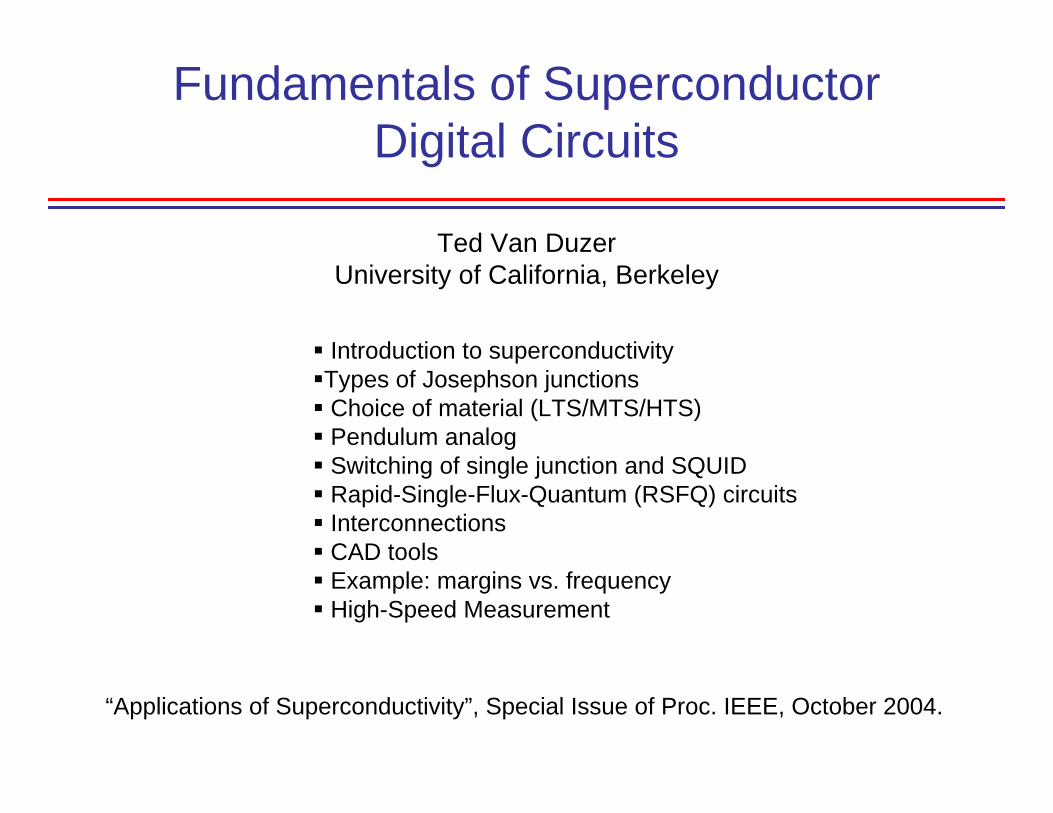
Fundamentals of Superconductor Digital Circuits Ted Van Duzer University of California, Berkeley Introduction to superconductivity Types of Josephson junctions Choice of material (LTS/MTS/HTS) Pendulum analog Switching of single junction and SQUID Rapid-Single-Flux-Quantum (RSFQ) circuits Interconnections CAD tools Example: margins vs. frequency High-Speed Measurement “Applications of Superconductivity”, Special Issue of Proc. IEEE, October 2004.
Transcript of Fundamentals of Superconductor Digital...
Fundamentals of Superconductor Digital Circuits
Ted Van DuzerUniversity of California, Berkeley
Introduction to superconductivityTypes of Josephson junctionsChoice of material (LTS/MTS/HTS)Pendulum analogSwitching of single junction and SQUID Rapid-Single-Flux-Quantum (RSFQ) circuitsInterconnectionsCAD toolsExample: margins vs. frequencyHigh-Speed Measurement
“Applications of Superconductivity”, Special Issue of Proc. IEEE, October 2004.

Introduction to Superconductivity
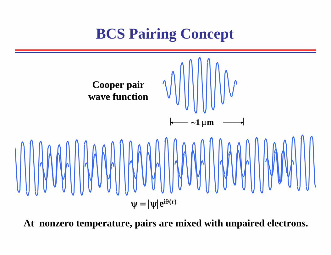
ψ = |ψ|eiθ(r)
BCS Pairing Concept
Cooper pairwave function
∼1 µm
At nonzero temperature, pairs are mixed with unpaired electrons.
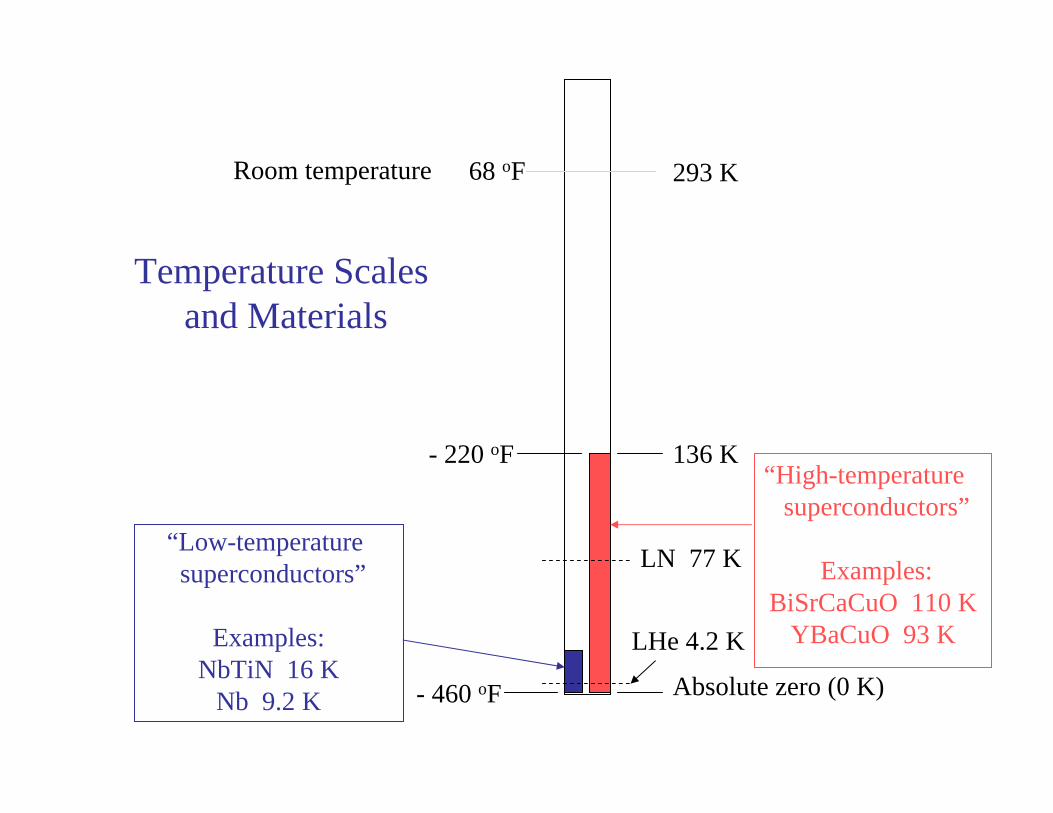
Absolute zero (0 K)
68 oF 293 K
- 460 oF
Room temperature
- 220 oF“High-temperature
superconductors”
Examples:BiSrCaCuO 110 K
YBaCuO 93 K
“Low-temperature superconductors”
Examples:NbTiN 16 K
Nb 9.2 K
136 K
LHe 4.2 K
LN 77 K
Temperature Scales and Materials
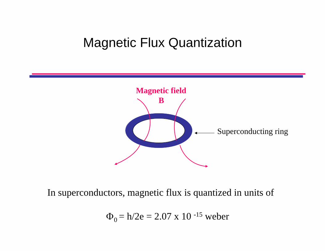
Magnetic Flux Quantization
Magnetic field B
In superconductors, magnetic flux is quantized in units of
Φ0 = h/2e = 2.07 x 10 -15 weber
Superconducting ring
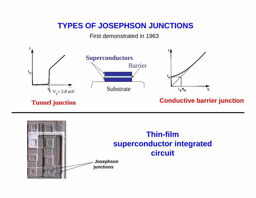
Thin-filmsuperconductor integrated
circuitJosephsonjunctions
TYPES OF JOSEPHSON JUNCTIONS
Tunnel junction Conductive barrier junctionVg= 2.8 mV
SuperconductorsBarrier
Substrate
First demonstrated in 1963
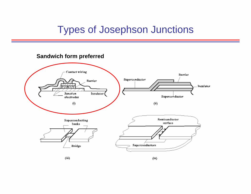
Types of Josephson Junctions
Sandwich form preferred
Digital Applications
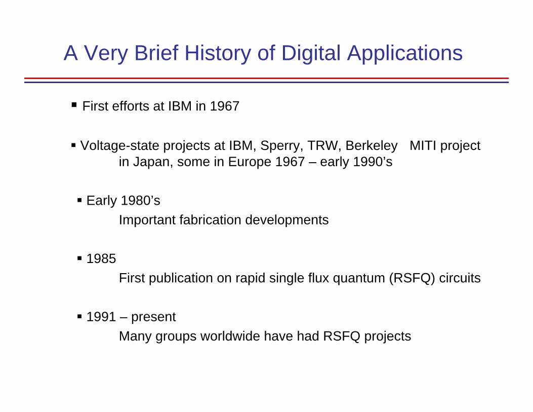
A Very Brief History of Digital Applications
First efforts at IBM in 1967
Voltage-state projects at IBM, Sperry, TRW, Berkeley MITI project in Japan, some in Europe 1967 – early 1990’s
Early 1980’sImportant fabrication developments
1985 First publication on rapid single flux quantum (RSFQ) circuits
1991 – present Many groups worldwide have had RSFQ projects
Issues in Digital Circuits
• Large numbers of devices (many thousands for useful circuits)
• Need for CAD tools (Some tools made for semiconductors are usable, but others need modification)
• Small margins (The allowed variation of power supply level)
• No gain (unlike transistor circuits)
• Lack of adequate memory (4-kbit memory demonstrated)
• Layout for flux management (1 cm2 chip has 500 flux quantaif B = 0.1 mG . Circuits must be protected.)

Device Technologyfor
Digital Applications
Choosing a Technology
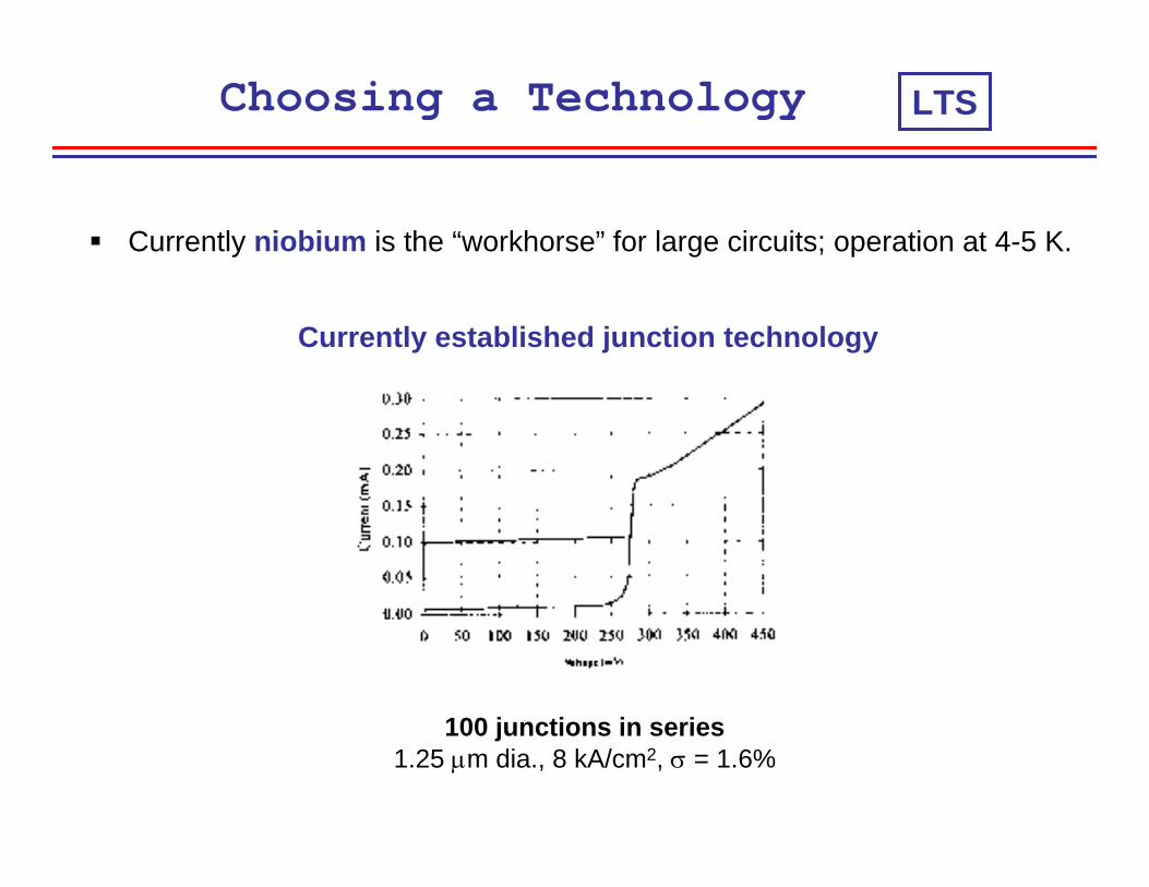
Currently niobium is the “workhorse” for large circuits; operation at 4-5 K.
100 junctions in series1.25 µm dia., 8 kA/cm2, σ = 1.6%
LTS
Currently established junction technology
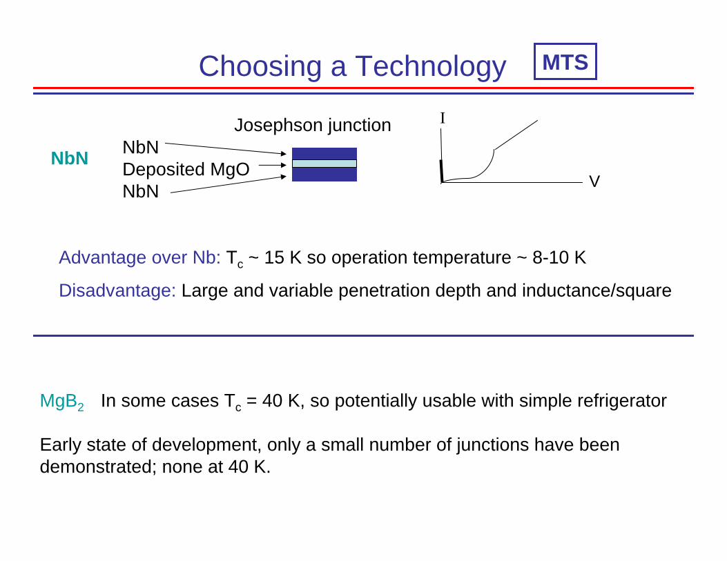
Choosing a Technology MTS
Advantage over Nb: Tc ~ 15 K so operation temperature ~ 8-10 K
Disadvantage: Large and variable penetration depth and inductance/square
MgB2 In some cases Tc = 40 K, so potentially usable with simple refrigerator
Early state of development, only a small number of junctions have been demonstrated; none at 40 K.
NbN NbNDeposited MgONbN
Josephson junction I
V
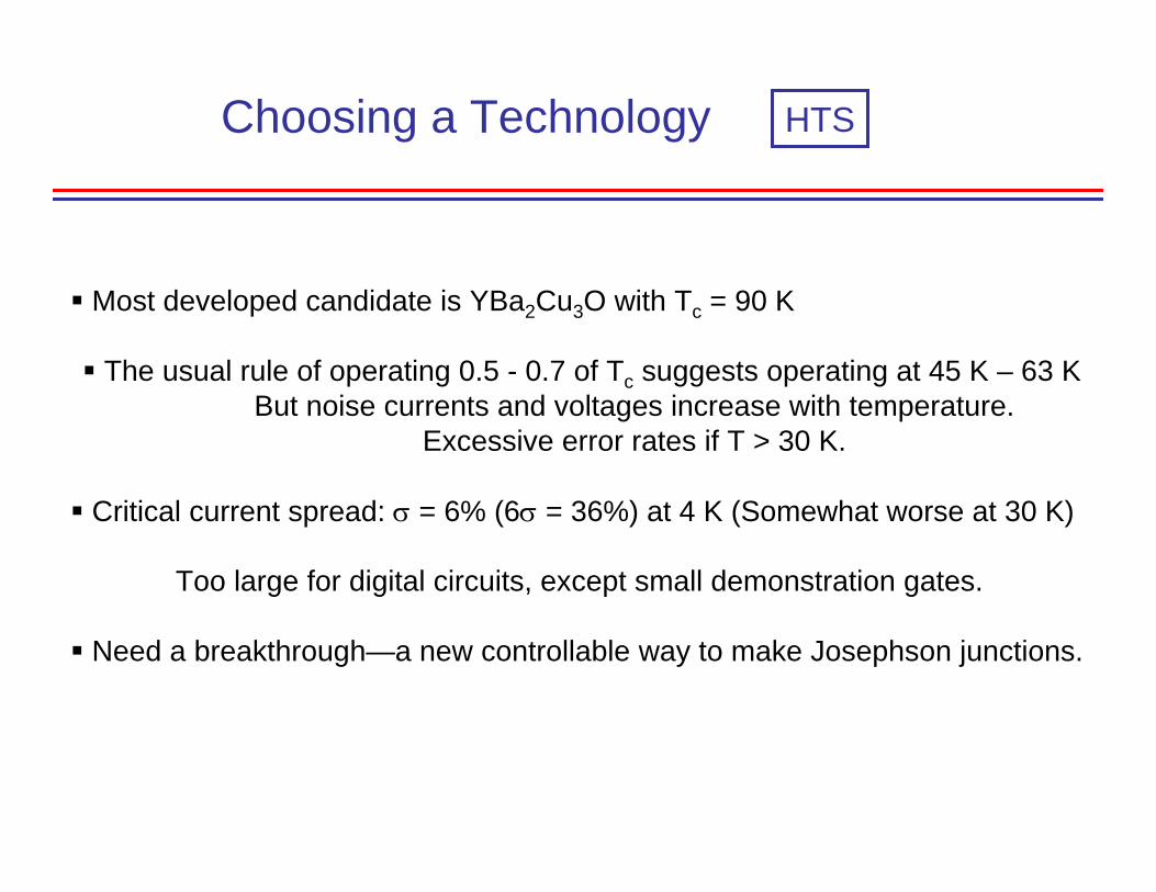
Choosing a Technology HTS
Most developed candidate is YBa2Cu3O with Tc = 90 K
The usual rule of operating 0.5 - 0.7 of Tc suggests operating at 45 K – 63 K But noise currents and voltages increase with temperature.
Excessive error rates if T > 30 K.
Critical current spread: σ = 6% (6σ = 36%) at 4 K (Somewhat worse at 30 K)
Too large for digital circuits, except small demonstration gates.
Need a breakthrough—a new controllable way to make Josephson junctions.
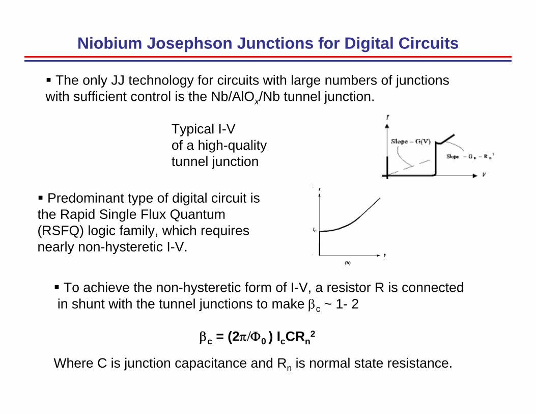
Niobium Josephson Junctions for Digital Circuits
Typical I-Vof a high-quality tunnel junction
Predominant type of digital circuit is the Rapid Single Flux Quantum (RSFQ) logic family, which requires nearly non-hysteretic I-V.
To achieve the non-hysteretic form of I-V, a resistor R is connectedin shunt with the tunnel junctions to make βc ~ 1- 2
βc = (2π/Φ0 ) IcCRn2
Where C is junction capacitance and Rn is normal state resistance.
The only JJ technology for circuits with large numbers of junctions with sufficient control is the Nb/AlOx/Nb tunnel junction.
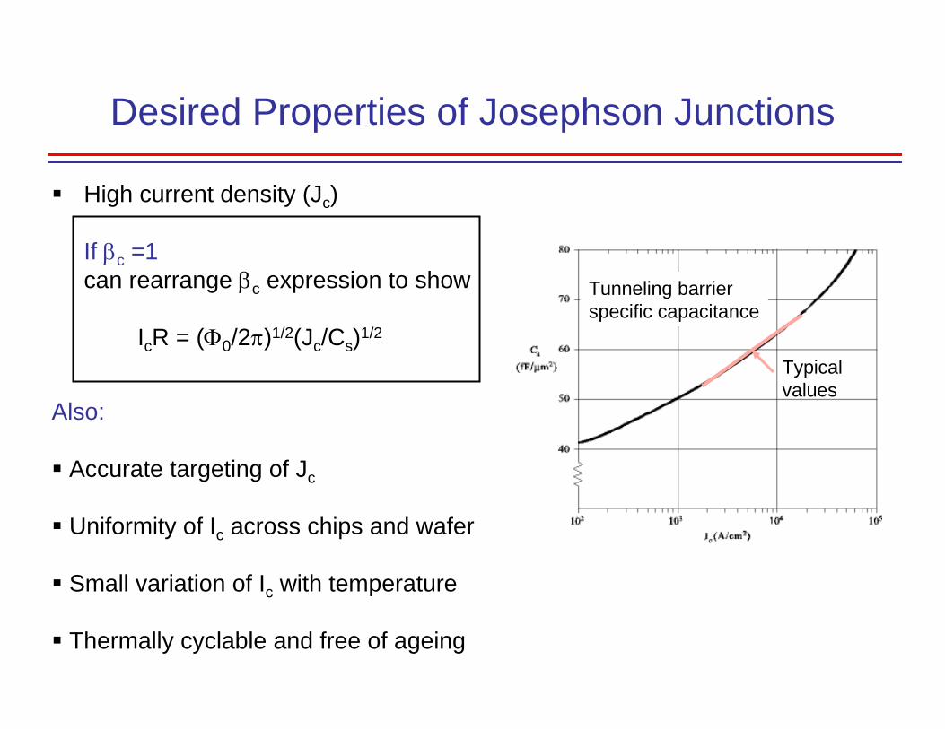
Desired Properties of Josephson Junctions
High current density (Jc)
If βc =1can rearrange βc expression to show
IcR = (Φ0/2π)1/2(Jc/Cs)1/2
Also:
Accurate targeting of Jc
Uniformity of Ic across chips and wafer
Small variation of Ic with temperature
Thermally cyclable and free of ageing
Tunneling barrierspecific capacitance
Typical values
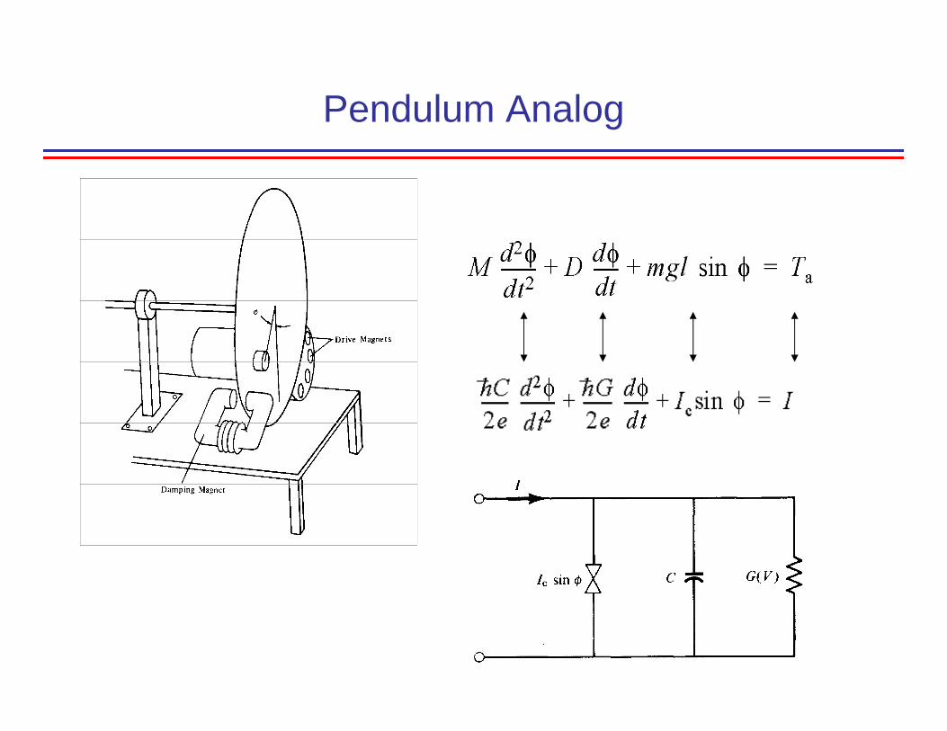
Pendulum Analog
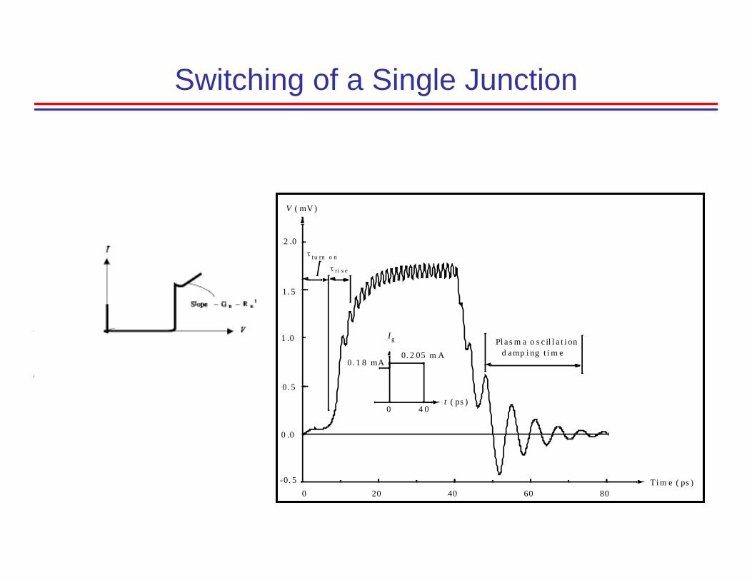
Switching of a Single Junction
0 20 40 60 80-0. 5
0. 5
1. 5
0 .0
1 .0
2 .0
V ( mV )
Ti m e ( ps )
τ t u rn o n
τ ri s e
Pl a s m a o s c il l a t i on d a mp i ng t i m e
Ig
0. 1 8 mA0. 2 05 m A
t ( ps )0 4 0
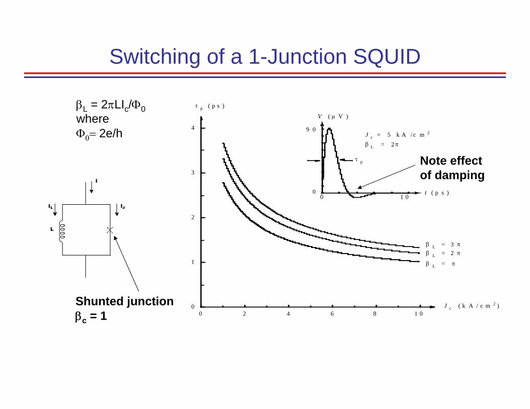
Switching of a 1-Junction SQUID
0 2 4 6 8 1 00
1
2
3
4
0
9 0
0 1 0t ( p s )
V ( µ V )
τ p
J c = 5 k A / c m 2
β L = 2 π
τ p ( p s )
J c ( k A / c m 2 )
β L = 3 πβ L = 2 π
β L = π
Shunted junctionβc = 1
Note effect of damping
βL = 2πLIc/Φ0where Φ0= 2e/h
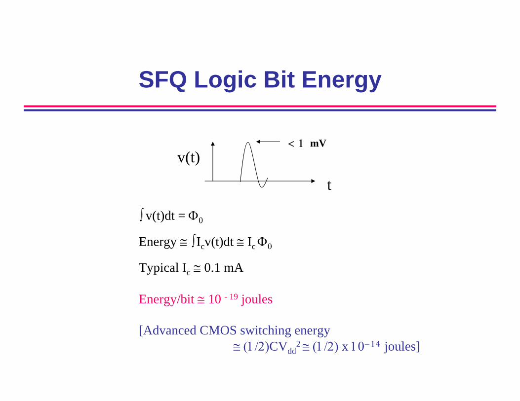
SFQ Logic Bit Energy
v(t)
t
< 1 mV
∫ v(t)dt = Φ0
Energy ≅ ∫ Icv(t)dt ≅ Ic Φ0
Typical Ic ≅ 0.1 mA
Energy/bit ≅ 10 - 19 joules
[Advanced CMOS switching energy ≅ (1/2)CVdd
2 ≅ (1/2) x 10− 14 joules]
Rapid-Single-Flux-Quantum (RSFQ) Logic Family
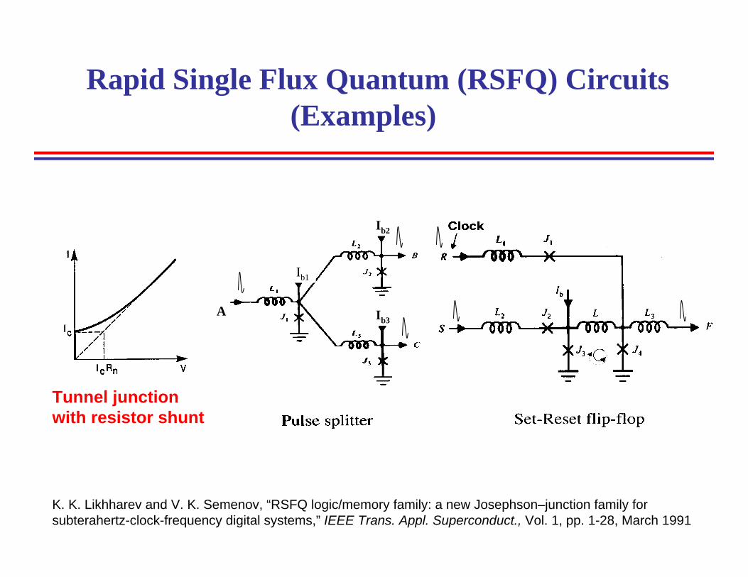
Rapid Single Flux Quantum (RSFQ) Circuits(Examples)
K. K. Likhharev and V. K. Semenov, “RSFQ logic/memory family: a new Josephson–junction family for subterahertz-clock-frequency digital systems,” IEEE Trans. Appl. Superconduct., Vol. 1, pp. 1-28, March 1991
A
Ib2
Ib1
Ib3
Tunnel junction with resistor shunt

HYPRES
Non-storage Inductance (~6 pH)
Junction Shunt (~1 Ω)
Junctions of different area(min. area = 3 µm x 3 µm)
Storage Inductance (~12 pH)
Toggle Flip-Flop Layout
RSFQ Gate Physical Layout on IC
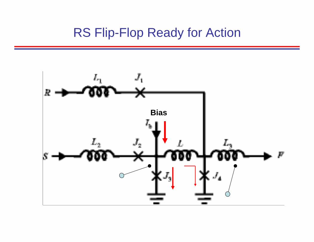
RS Flip-Flop Ready for Action
Bias
. .
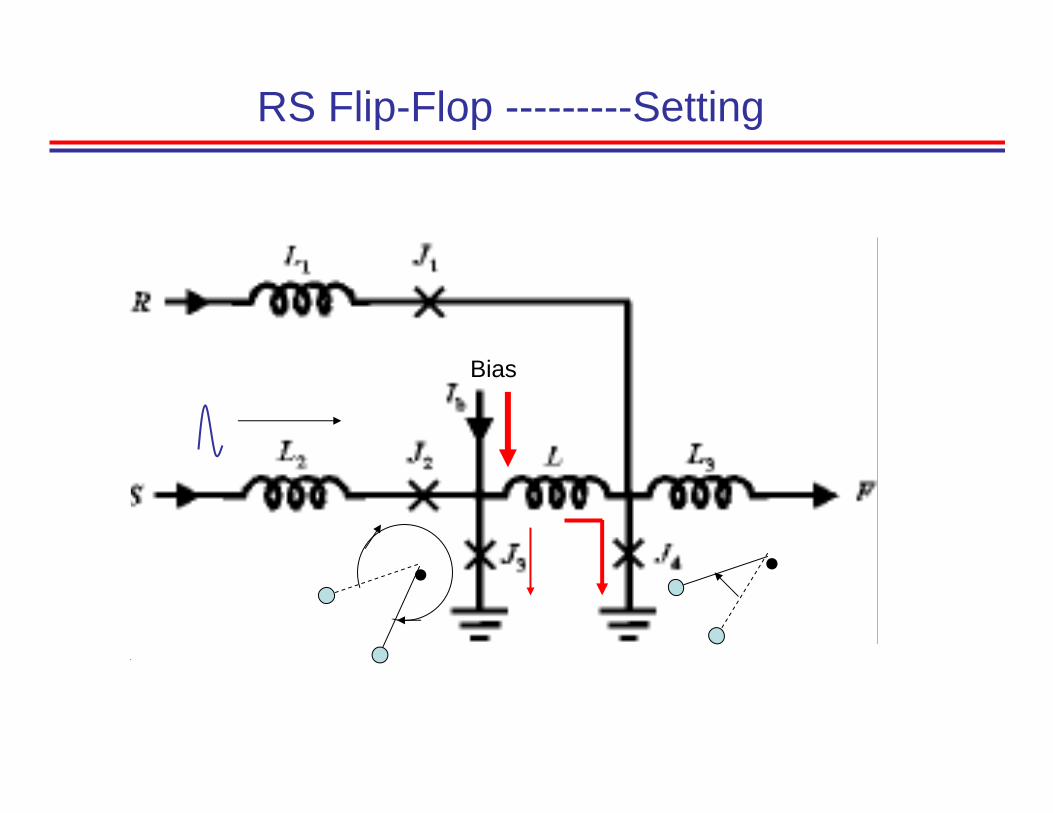
RS Flip-Flop ---------Setting
Bias
. .
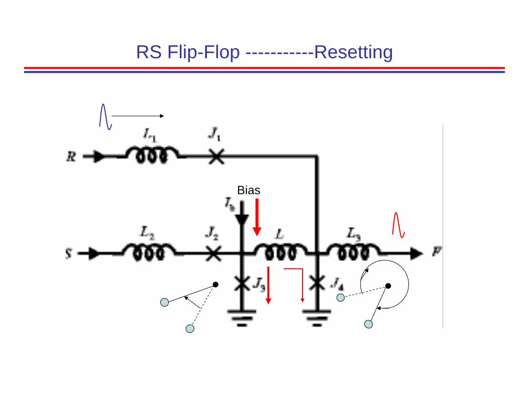
RS Flip-Flop -----------Resetting
Bias
. .
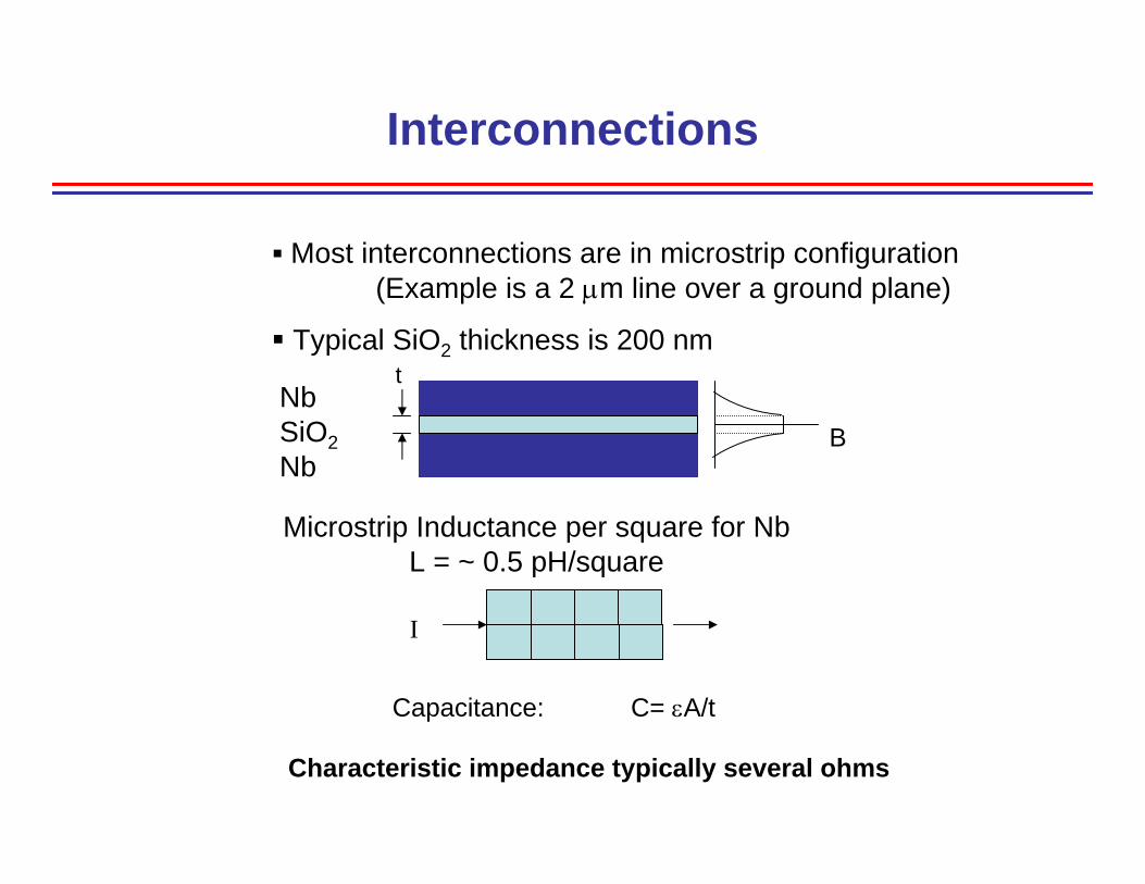
Microstrip Inductance per square for NbL = ~ 0.5 pH/square
I
Interconnections
BNbSiO2Nb
t
Most interconnections are in microstrip configuration(Example is a 2 µm line over a ground plane)
Typical SiO2 thickness is 200 nm
Capacitance: C= εA/t
Characteristic impedance typically several ohms
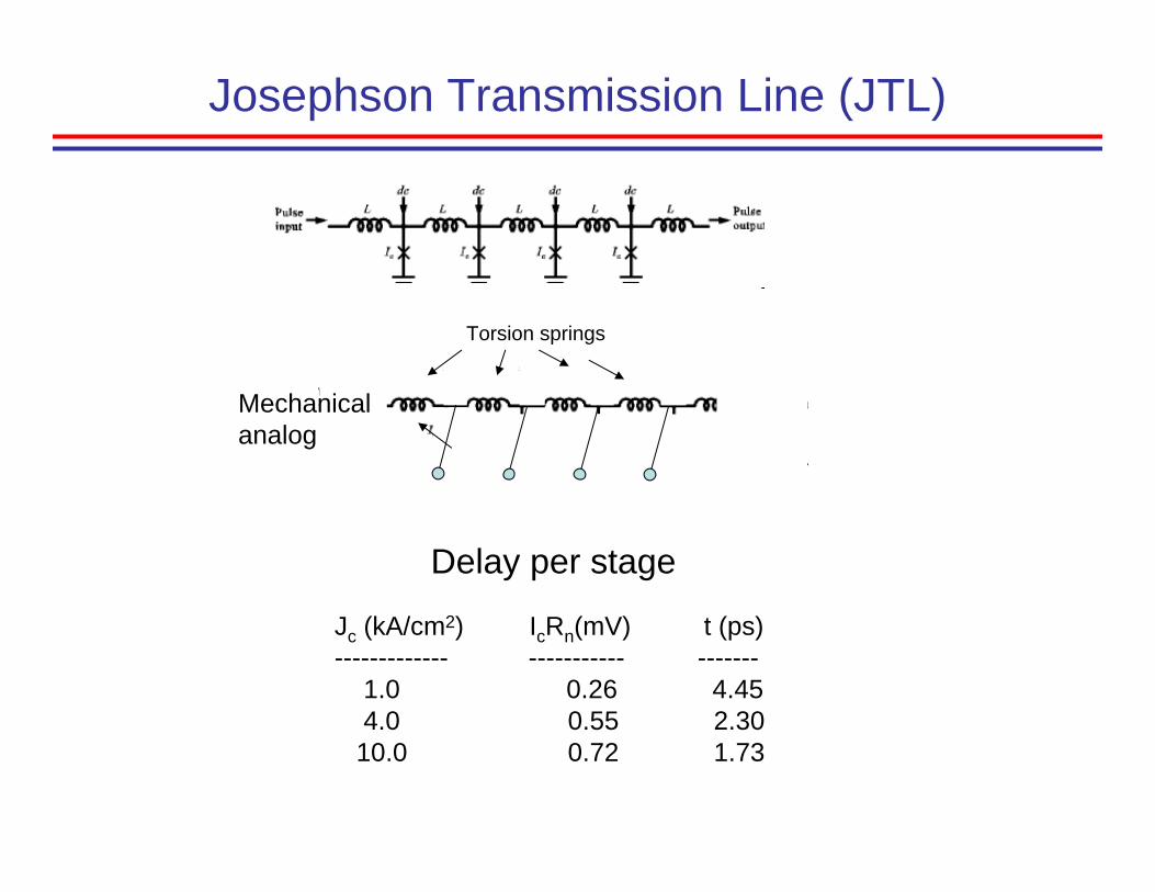
Josephson Transmission Line (JTL)
Jc (kA/cm2) IcRn(mV) t (ps)------------- ----------- -------
1.0 0.26 4.454.0 0.55 2.3010.0 0.72 1.73
Torsion springs
Mechanical analog
Delay per stage
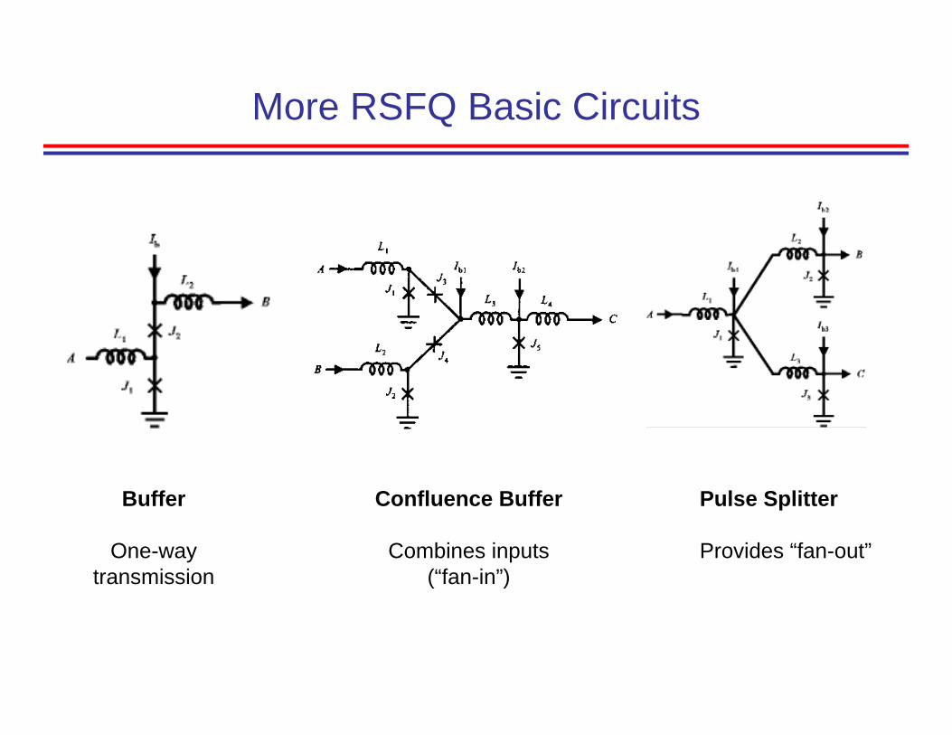
More RSFQ Basic Circuits
Buffer
One-way transmission
Confluence Buffer
Combines inputs(“fan-in”)
Pulse Splitter
Provides “fan-out”
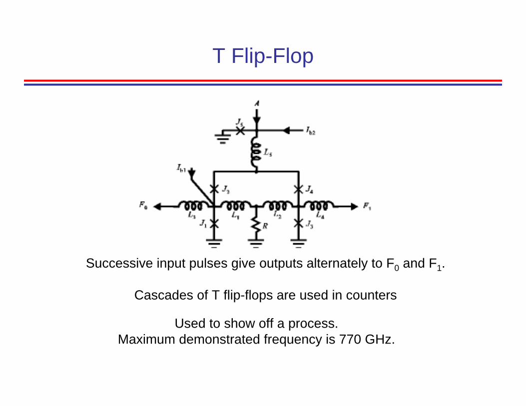
T Flip-Flop
Successive input pulses give outputs alternately to F0 and F1.
Cascades of T flip-flops are used in counters
Used to show off a process. Maximum demonstrated frequency is 770 GHz.
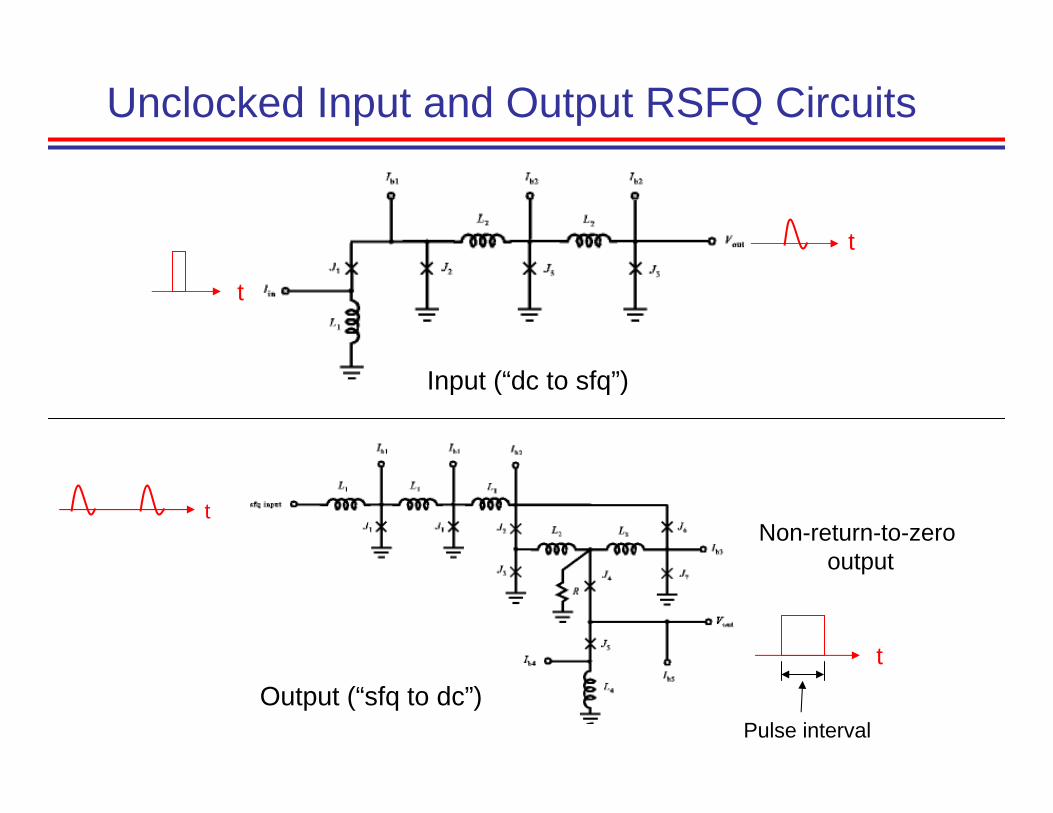
Unclocked Input and Output RSFQ Circuits
Input (“dc to sfq”)
t
t
t
Pulse intervalOutput (“sfq to dc”)
tNon-return-to-zero
output
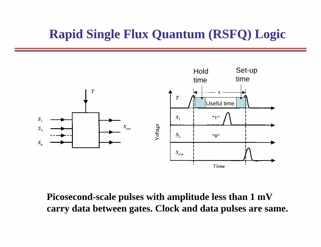
Picosecond-scale pulses with amplitude less than 1 mVcarry data between gates. Clock and data pulses are same.
Rapid Single Flux Quantum (RSFQ) Logic
Holdtime
Set-up time
Useful time
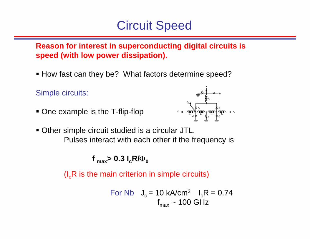
Circuit SpeedReason for interest in superconducting digital circuits is speed (with low power dissipation).
How fast can they be? What factors determine speed?
Simple circuits:
One example is the T-flip-flop
Other simple circuit studied is a circular JTL.Pulses interact with each other if the frequency is
f max> 0.3 IcR/Φ0
(IcR is the main criterion in simple circuits)
For Nb Jc = 10 kA/cm2 IcR = 0.74fmax ~ 100 GHz
Larger Circuits
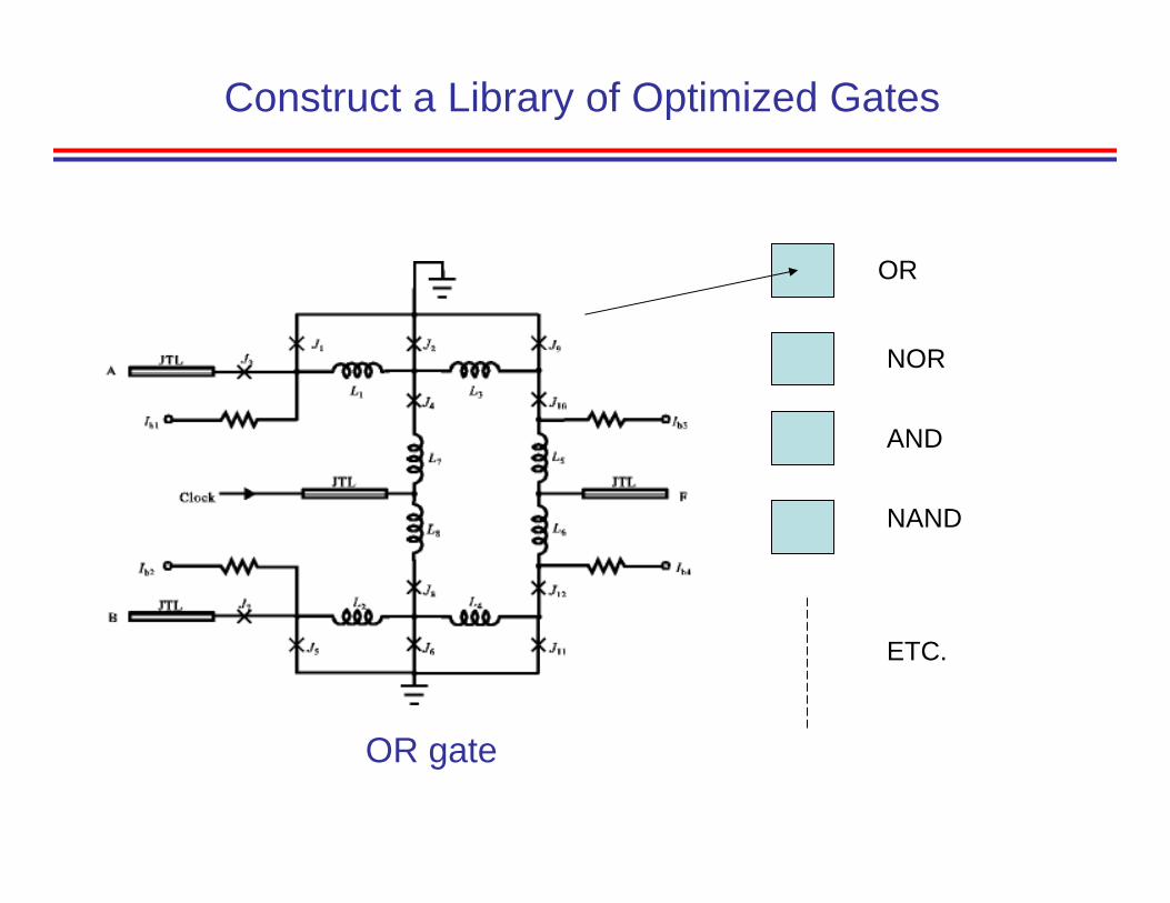
Construct a Library of Optimized Gates
OR gate
OR
NOR
AND
NAND
ETC.
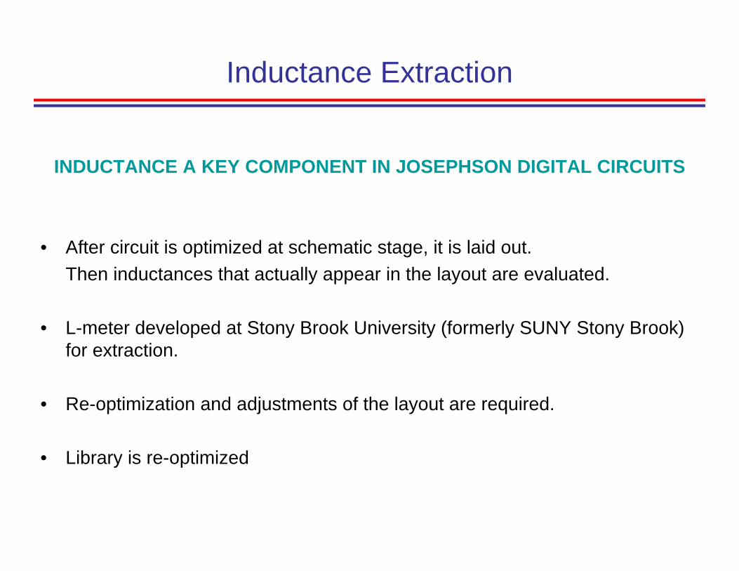
Inductance Extraction
INDUCTANCE A KEY COMPONENT IN JOSEPHSON DIGITAL CIRCUITS
• After circuit is optimized at schematic stage, it is laid out. Then inductances that actually appear in the layout are evaluated.
• L-meter developed at Stony Brook University (formerly SUNY Stony Brook) for extraction.
• Re-optimization and adjustments of the layout are required.
• Library is re-optimized
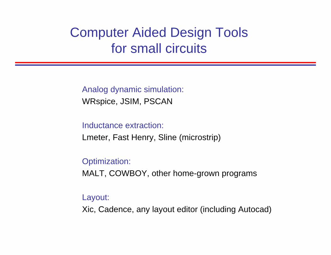
Computer Aided Design Toolsfor small circuits
Analog dynamic simulation:WRspice, JSIM, PSCAN
Inductance extraction:Lmeter, Fast Henry, Sline (microstrip)
Optimization:MALT, COWBOY, other home-grown programs
Layout:Xic, Cadence, any layout editor (including Autocad)
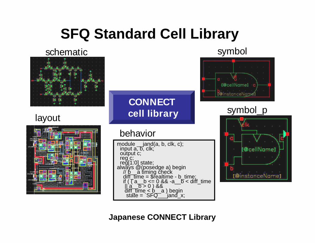
SFQ Standard Cell Libraryschematic
behavior
symbol_playout
module __jand(a, b, clk, c);input a, b, clk;output c;reg c;reg[1:0] state;
always @(posedge a) begin// b__a timing checkdiff_time = $realtime - b_time;if ( ( a__b <= 0 && -a__b < diff_time|| a__b > 0 ) &&diff_time < b__a ) beginstate = `SFQ___jand_x;
symbol
CONNECTcell library
Japanese CONNECT Library
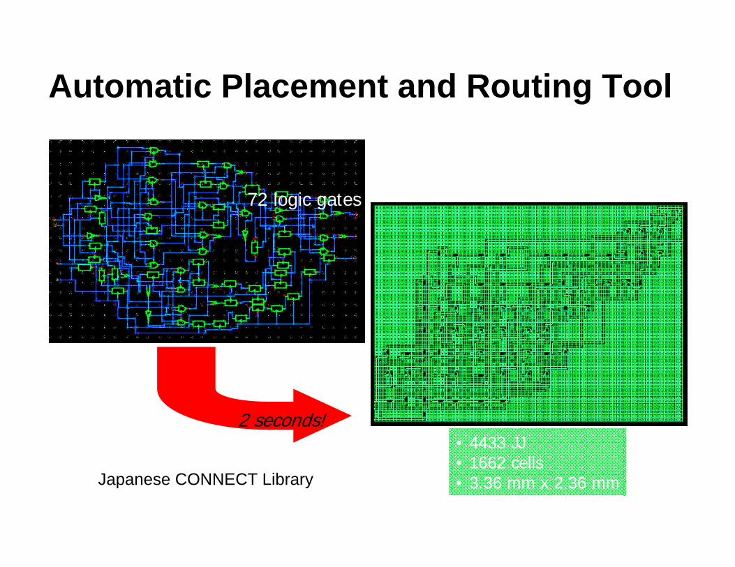
Automatic Placement and Routing Tool
72 logic gates
• 4433 JJ• 1662 cells• 3.36 mm x 2.36 mm
2 seconds!
Japanese CONNECT Library
An Example of a Circuit Design and Layoutat Berkeley
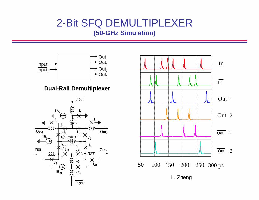
2-Bit SFQ DEMULTIPLEXER(50-GHz Simulation)
In
In
Out 1
Out 2
Out 2
Out 1
50 100 150 200 250 300 ps
InputInput
Out1Out1Out2Out2
Dual-Rail Demultiplexer
L. Zheng
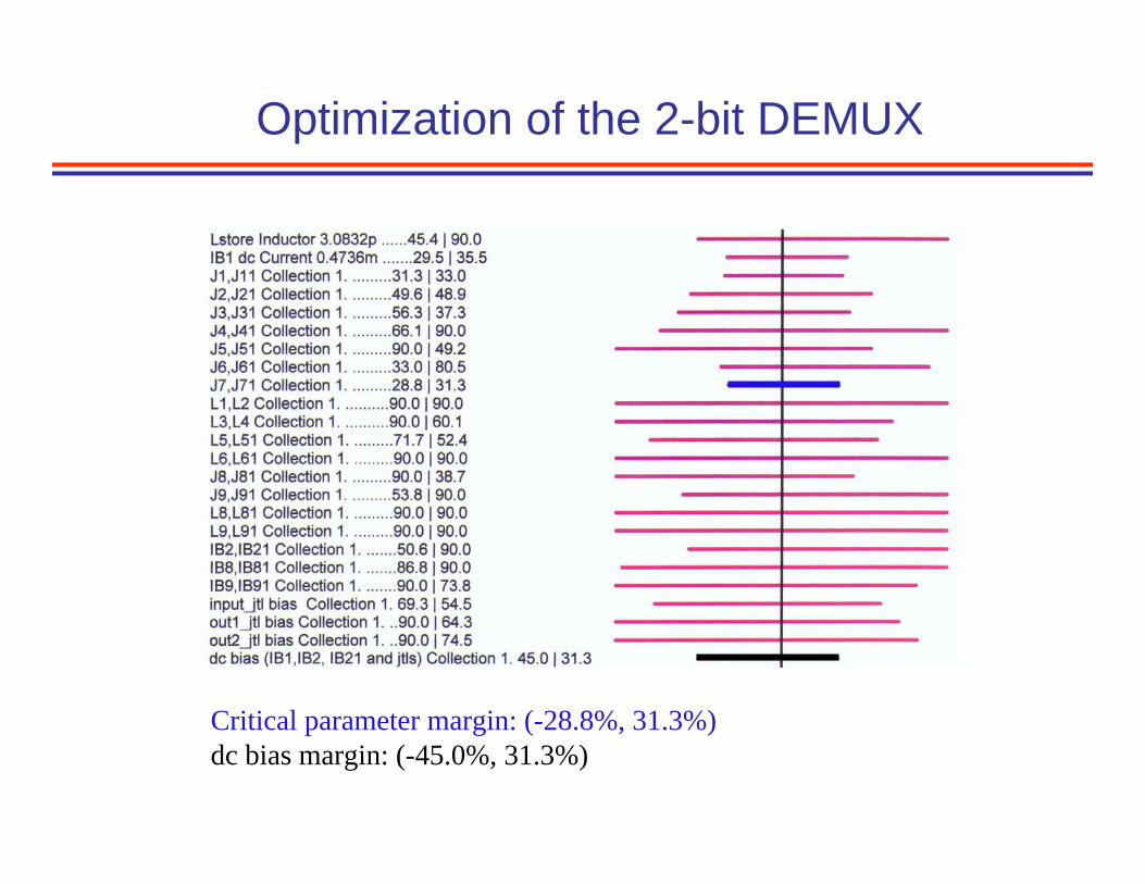
Optimization of the 2-bit DEMUX
Critical parameter margin: (-28.8%, 31.3%)dc bias margin: (-45.0%, 31.3%)
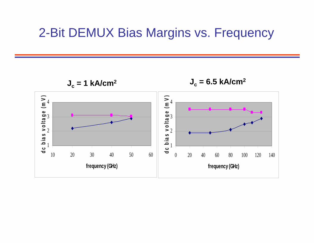
2-Bit DEMUX Bias Margins vs. Frequency
1
2
3
4
10 20 30 40 50 60
frequency (GHz)
dc b
ias
volta
ge (m
V)
1
2
3
4
0 20 40 60 80 100 120 140
frequency (GHz)dc
bia
s vo
ltage
(mV)
Jc = 1 kA/cm2 Jc = 6.5 kA/cm2
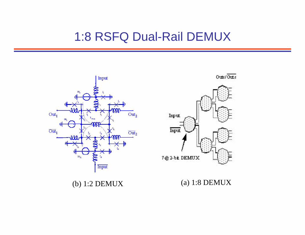
1:8 RSFQ Dual-Rail DEMUX
(b) 1:2 DEMUX (a) 1:8 DEMUX
40
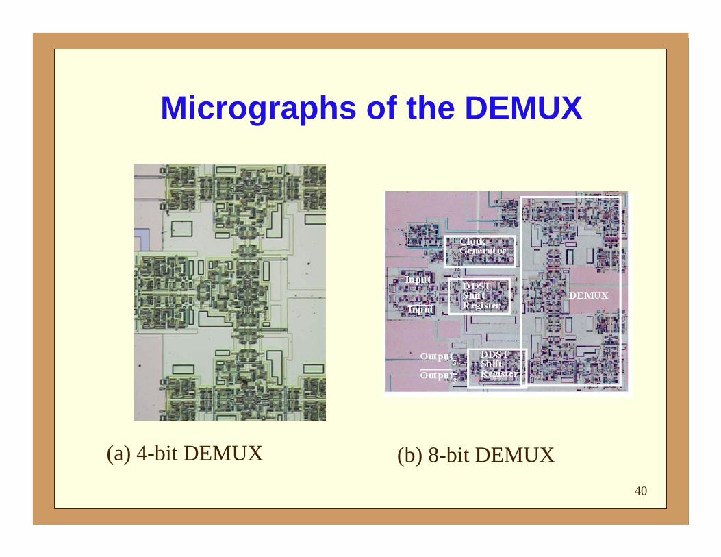
Micrographs of the DEMUX
(a) 4-bit DEMUX (b) 8-bit DEMUX
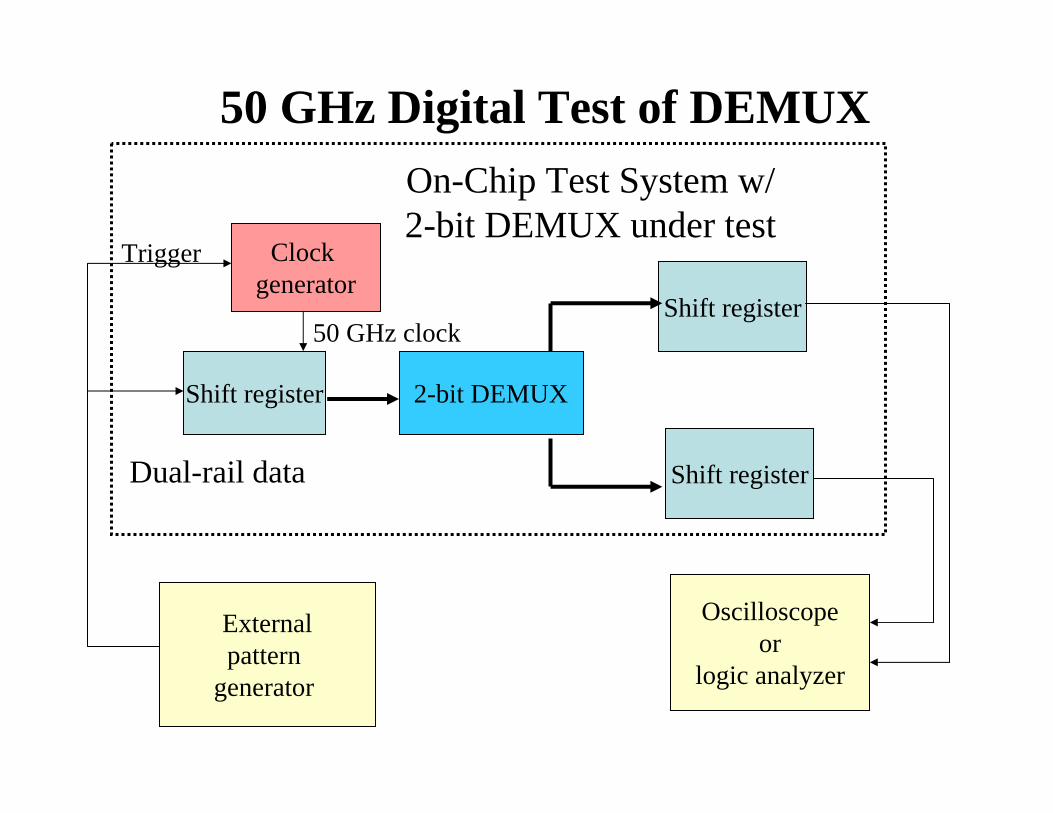
50 GHz Digital Test of DEMUX
Externalpattern
generator
Oscilloscopeor
logic analyzer
Clock generator
Shift register
Shift register
2-bit DEMUXShift register
Trigger
On-Chip Test System w/ 2-bit DEMUX under test
50 GHz clock
Dual-rail data

And there’s more to the story------