Fundamental Limitations to CMOS...
19
Fundamental Limitations to CMOS Scaling Presented by: Sijia He Xiaoming Guo Bangqi Xu October 29, 2013
-
Upload
truonghanh -
Category
Documents
-
view
224 -
download
1
Transcript of Fundamental Limitations to CMOS...
Fundamental Limitations to CMOS Scaling
Presented by: Sijia He
Xiaoming Guo Bangqi Xu
October 29, 2013

Outline � Motivation for scaling
� Fabrication difficulties
� High leakage current
� Possible solutions

Motivation for Scaling � Scaling = Improving performance

Motivation for Scaling � More transistors --> Higher performance � Less delay time --> Higher frequency � Less VDD --> Lower power consumption
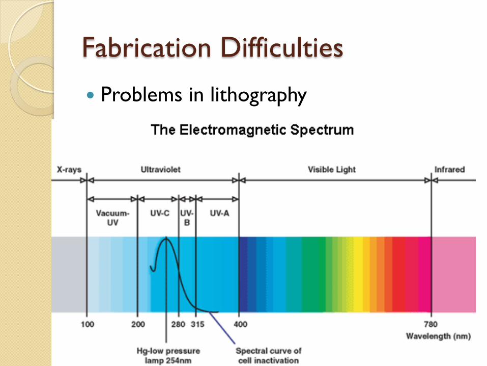
Fabrication Difficulties � Problems in lithography

Fabrication Difficulties � State-of-the-art lithography: 193nm UV � Next Generation: 13.5nm EUV
Fabrication Difficulties � Problems of 13.5nm EUV: Cost! ◦ Need to change the entire lithography
equipment ◦ Still take some time to reach 14-nm
technology or lower. ◦ As a result: Cost overwhelms benefits.

High Leakage Current � P = PSWITCH+PSHORT+PLEAK
High Leakage Current � Five major sources of leakage current: ◦ Gate oxide tunneling leakage ◦ Subthreshold leakage ◦ Reverse-bias junction leakage ◦ Gate induced drain leakage ◦ Gate current due to hot-carrier injection
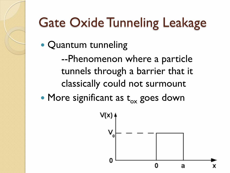
Gate Oxide Tunneling Leakage � Quantum tunneling
--Phenomenon where a particle tunnels through a barrier that it classically could not surmount
� More significant as tox goes down
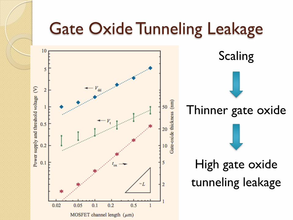
Gate Oxide Tunneling Leakage Scaling
Thinner gate oxide
High gate oxide tunneling leakage

Subthreshold Leakage � Current is not 0 when the transistor is off � From lecture slides 5, we have equation
S=n(kT/q)ln(10) S: Change in VGS for ID to change 10x
� Scaling -> Smaller threshold voltage ->
Nearer to the VGS = 0 -> Higher subthreshold leakage
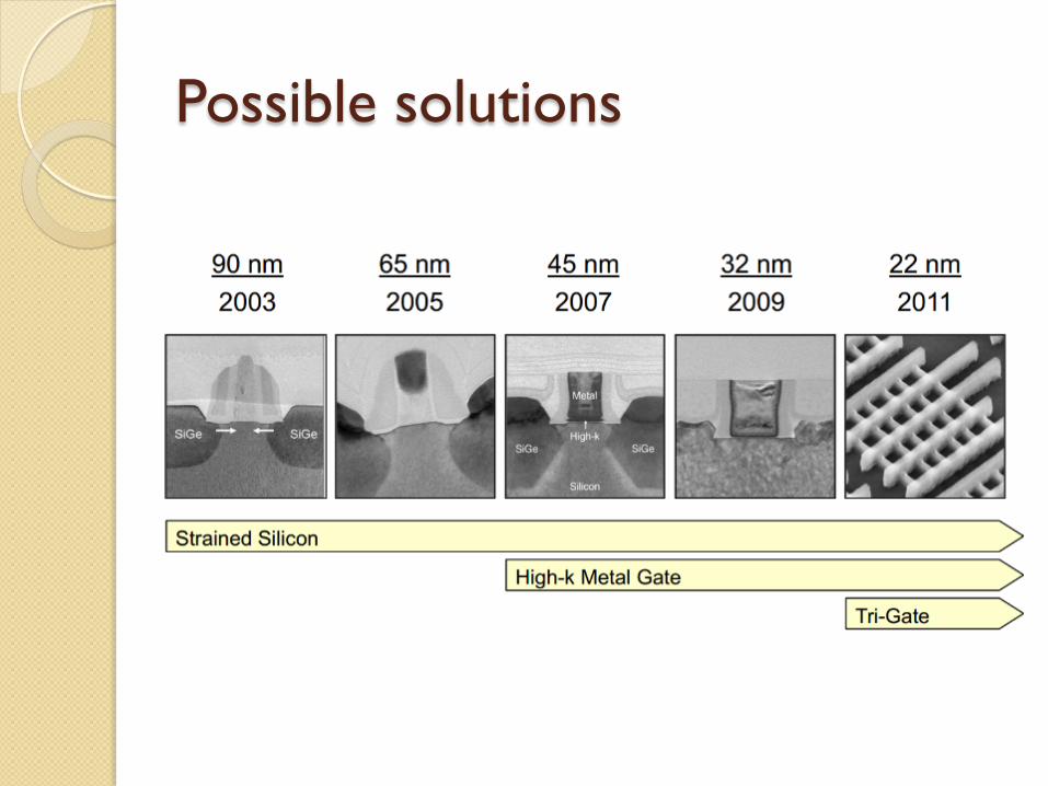
Possible solutions

Strained Silicon
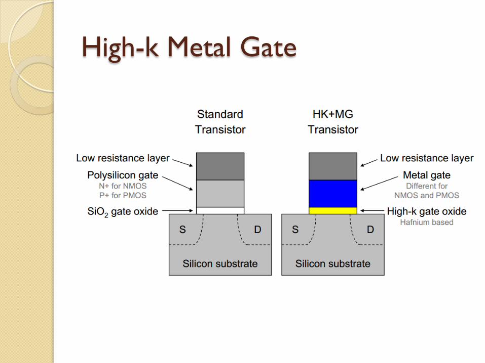
High-k Metal Gate
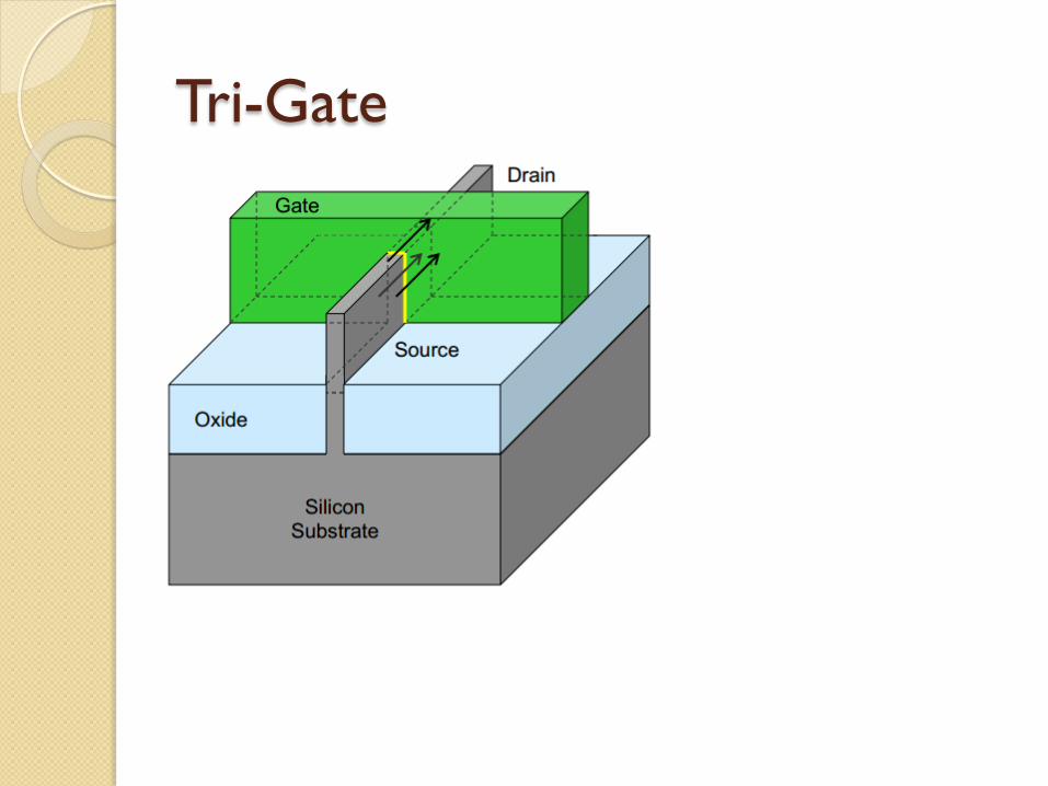
Tri-Gate
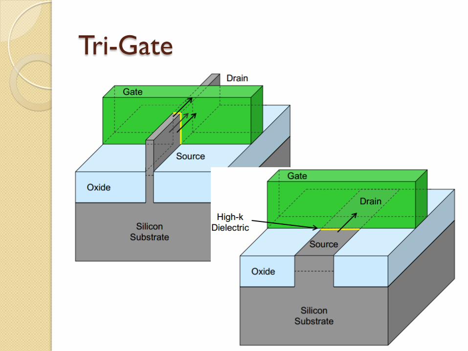
Tri-Gate

Reference: � Intel’s Revolutionary 22 nm Transistor Technology,
http://download.intel.com/newsroom/kits/22nm/pdfs/22nm-Details_Presentation.pdf
� Dmitri Nikonov, CMOS Scaling, http://nanohub.org/resources/18348/download/NikonovBeyondCMOS_1_scaling.pdf
� http://3.bp.blogspot.com/_Se0VANaI9uM/R9zN-QzfETI/AAAAAAAAAQc/V1r5pgUAHZk/s1600-h/leakage+vs+power.jpeg
� Y. Taur, CMOS design near the limit of scaling, http://paginas.fe.up.pt/~jcf/PCVLSI/2003-04/taur.pdf
� http://www.coachingworks.de/workinprogress/wp-content/uploads/2010/04/02_UV_Light_Spectrum.gif

Reference: � Mark Bohr, Silicon Technology Leadership for the
Mobility era, http://www.intel.com/content/dam/www/public/us/en/documents/presentation/silicon-technology-leadership-presentation.pdf
� http://www.ixbt.com/cpu/semiconductor/intel-65nm/lith_challenge.jpg
� http://en.wikipedia.org/wiki/Quantum_tunnelling � http://en.wikipedia.org/wiki/Potential_barrier � http://citeseerx.ist.psu.edu/viewdoc/download?
doi=10.1.1.87.5308&rep=rep1&type=pdf � http://download.intel.com/pressroom/kits/45nm/
Press45nm107_FINAL.pdf