Full Bridge LLC ZVS Resonant Converter Based on … One: High Efficiency, Dual SiC MOSFET in...
29
Full Bridge LLC ZVS Resonant Converter Based on Gen2 SiC Power MOSFET Cree Power Application Engineering Rev. 2 Copyright © 2014, Cree Inc. 1
Transcript of Full Bridge LLC ZVS Resonant Converter Based on … One: High Efficiency, Dual SiC MOSFET in...

Full Bridge LLC ZVS Resonant Converter Based on Gen2 SiC Power MOSFET
Cree Power Application Engineering
Rev. 2
Copyright © 2014, Cree Inc. 1

Confidential Copyright © 2012, Cree Inc. 2
SiC MOSFETs can simplify ZVS converter designs AND offer the following advantages: § Lower system cost § Improved performance § Smaller size
ZVS converters are typically used in the following applications: § Industrial power supply § Telecommunications power supply § EV Battery charger
Overview

Confidential 3
Silicon: 600V MOS Three-level LLC Full bridge Typical switching frequency: 100KHZ-200KHZ
Silicon Carbide: 1200V SiC MOS Two-level FB ZVS LLC resonant Target switching: >200KZ-400KHZ Can reduce BOM cost and improve efficiency
Copyright © 2014, Cree Inc.
Three-level (3L) Resonant Tank Two-level (2L) Resonant Tank
Si to SiC
Simplify with SiC – Example 1

Confidential 4
Simplify with SiC – Example 2
Silicon: 600V MOS Interleaved Two level LLC Full bridge Typical switching frequency: 100KHZ-200KHZ
Silicon Carbide: 1200V SiC MOS Two-level FB ZVS LLC resonant Target switching: >200KZ-400KHZ Can reduce BOM cost and improve efficiency
Copyright © 2014, Cree Inc.
Two-level (2L) Resonant Tank
Two-level 1
Two-level 2
Resonant Tank 1
Resonant Tank 2
Si to SiC

Confidential
TO-247 MOSFET Parameters Comparison (Gen2 1.2kV SiC MOSFET Vs 650V Si CoolMOS)
5 Copyright © 2014, Cree Inc.
Parameters SiC MOS C2M0160120D
Si CoolMOS SPW47N60CFD
Si CoolMOS IPW65R110CFD
Breakdown Voltage @Tjmax 1200V 650V 650V
Rdson @Tc=110degC 0.22Ω 0.14Ω (x2 for three-level)
0.19Ω (x2 for three-level)
Ciss @f=1MHZ VDS=100V 527pF 7700pF 3240pF
Coss @f=1MHz VDS=100V 100pF 300pF 160pF
Crss @f=1MHz VDS=100V 5pF 10pF 8pF
Td(on)V Turn on delay time 7ns (VDD=800V) 30ns (VDD=400V) 16ns(VDD=400V)
Td(off)V Turn off delay time 13ns (VDD=800V) 100ns(VDD=400V) 68ns(VDD=400V)
Tr Rise time 12ns (VDD=800V) 30ns(VDD=400V) 11ns(VDD=400V)
Tf Fall time 7ns (VDD=800V) 15ns(VDD=400V) 6ns(VDD=400V)
Qg, typ 32.6nC 248nC 118nC
Body diode reverse recovery time trr
35ns 210ns 150ns
Body diode charge Qrr 0.120uC 2uC 0.8uC
Note: The comparison is based on the datasheets

Confidential
Gen2 SiC MOSFET Advantage in ZVS Converters
6 Copyright © 2014, Cree Inc.
§ Over 1.2kV blocking voltage.
§ Low Rdson to reduce conduction losses. § Lower turn off losses due to short fall
time and low Coss.
§ Short turn off delay time can reduce dead time.
§ Lower Qg will allow lower gate drive losses when switching frequency is high.
§ Low body diode trr and Qrr, which will reduce diode switching losses and electrical noise due to short reverse recovery time.
Simplifies Topology
Increases efficiency and power density.

Confidential
DC Gain Design with Resonant Tank Parameters
135KHZ Resonant frequency
Large passive LLC resonant tank
Copyright © 2014, Cree Inc.
Small passive LLC resonant tank
260KHZ Resonant frequency
Si to SiC
DC Gain Curve Lm=100uH Lr=15uH Cr=25nF
Lm=150uH Lr=35uH Cr=40nF
Frequency (KHZ)
Voltage Gain (M)
750V I/P DC Gain
700V I/P DC Gain
650V I/P DC Gain
Frequency (KHZ)
Voltage Gain (M)
fr1
2π Lr Cr⋅:= fr
1
2π Lr Cr⋅:=
Confidential
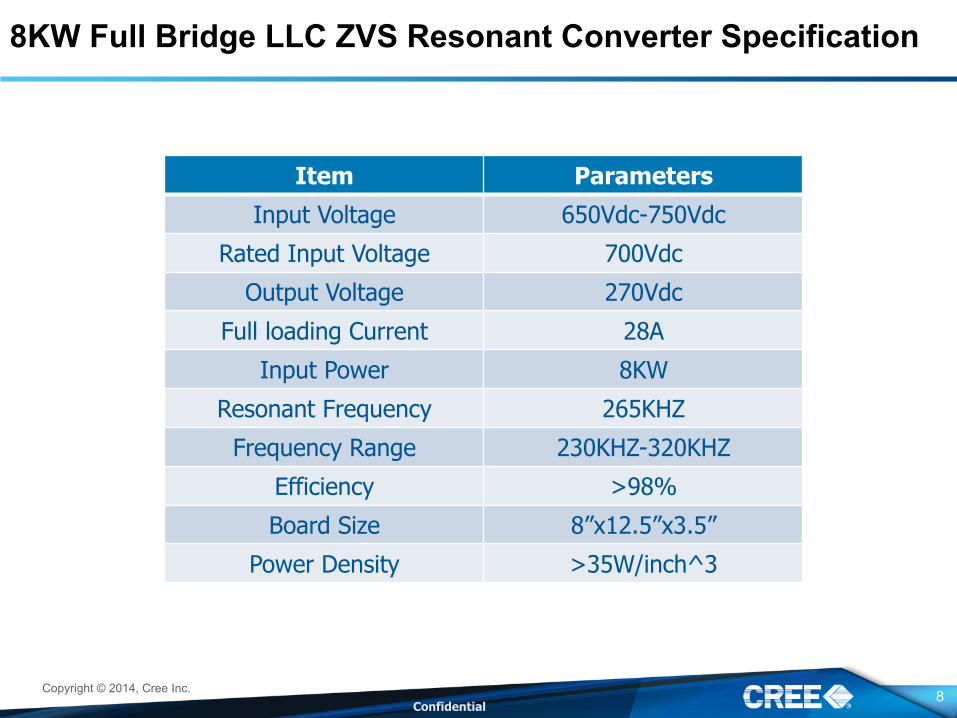
8KW Full Bridge LLC ZVS Resonant Converter Specification
8 Copyright © 2014, Cree Inc.
Item Parameters
Input Voltage 650Vdc-750Vdc
Rated Input Voltage 700Vdc
Output Voltage 270Vdc
Full loading Current 28A
Input Power 8KW
Resonant Frequency 265KHZ
Frequency Range 230KHZ-320KHZ
Efficiency >98%
Board Size 8”x12.5”x3.5”
Power Density >35W/inch^3

Confidential
Board Size of 8KW Full Bridge LLC Resonant Converter (Size: 8”x12.5”x3.5” )
9 Copyright © 2014, Cree Inc.
Input
Output
Resonant Tank Lm
Lr
Cr
SiC MOS with heatsink
SiC SBD
Controller Gate Driver

Confidential
Three-Level with Si Vs Two-level with SiC (8-10KW case)
10 Copyright © 2014, Cree Inc.
Items Three-level FB w/ Si MOS @ 120KHZ resonant freq.
Two-level FB w/ SiC MOS @ 260KHZ resonant freq.
MOSFETs 16pcs SPW47N60CFD 8pcs C2M0160120D
Flying diode 4pcs None Resonant Inductor 2pcs PQ3535 1pcs PQ3535 Lr=15uH
Magnetize transformer 2pcs PQ5050 1pcs PQ6560 Lm=100uH
Resonant Capacitors 35nF 25nF MOS Drivers 8pcs 4pcs

Waveforms

Confidential
Full Loading with 28A/270V and 700Vdc input
12 Copyright © 2014, Cree Inc.
ip(10A/div) Vab(500V/div)
VgsQ3(10Vdiv)
Q3
Q1
Q4
Q2C1 C2
C3 C4
Lr Cr
Lm
T1 DR1
DR2
Cf
Cbus
a
b
1200VSiC MOS
1200VSiC MOS
1200VSiC MOS
1200VSiC MOS
650V-800V
VgsQ4(10Vdiv)
Rise time
Body diode conduction current
Body diode conduction current
1us/div

Confidential
Half Loading with 14A/270V and 700Vdc input
13 Copyright © 2014, Cree Inc.
Q3
Q1
Q4
Q2C1 C2
C3 C4
Lr Cr
Lm
T1 DR1
DR2
Cf
Cbus
a
b
1200VSiC MOS
1200VSiC MOS
1200VSiC MOS
1200VSiC MOS
650V-800V
Rise time
Body diode conduction current
Body diode conduction current
ip(10A/div) Vab(500V/div)
VgsQ3(10Vdiv) VgsQ4(10Vdiv)
1us/div

Confidential 14 Copyright © 2014, Cree Inc.
Min Loading with 2A/270V and 700Vdc input
Rise time
Q3
Q1
Q4
Q2C1 C2
C3 C4
Lr Cr
Lm
T1 DR1
DR2
Cf
Cbus
a
b
1200VSiC MOS
1200VSiC MOS
1200VSiC MOS
1200VSiC MOS
650V-800V
ip(10A/div) Vab(500V/div)
VgsQ3(10Vdiv) VgsQ4(10Vdiv)
1us/div

Confidential
Full Loading with 28A/270V and 650Vdc input
15 Copyright © 2014, Cree Inc.
ip(10A/div) Vab(500V/div)
VgsQ3(10Vdiv)
Q3
Q1
Q4
Q2C1 C2
C3 C4
Lr Cr
Lm
T1 DR1
DR2
Cf
Cbus
a
b
1200VSiC MOS
1200VSiC MOS
1200VSiC MOS
1200VSiC MOS
650V-800V
VgsQ4(10Vdiv)
Rise time
Body diode conduct current
Body diode conduct current
1us/div

Confidential
Full Loading with 28A/270V and 750Vdc input
16 Copyright © 2014, Cree Inc.
ip(10A/div) Vab(500V/div)
VgsQ3(10Vdiv)
Q3
Q1
Q4
Q2C1 C2
C3 C4
Lr Cr
Lm
T1 DR1
DR2
Cf
Cbus
a
b
1200VSiC MOS
1200VSiC MOS
1200VSiC MOS
1200VSiC MOS
650V-800V
VgsQ4(10Vdiv)
Rise time
Body diode conduction current
Body diode conduction current
1us/div

Scenario One: High Efficiency, Dual SiC MOSFET in parallel per Switch
(SiC C2M0160120D Vs Si SPW47N60CFD)

Confidential
Calculation Losses Breakdown (700Vdc Input and 28A Output full load) @265KHZ SiC 2L and 135KHZ Si 3L (Dual MOS per switch)
18 Copyright © 2014, Cree Inc.
36.8W
15.2W
1.2W
2.72W 10.5W 9.9W 6.1W
6.3W
43.2W
18W SiC MOS Conduction
SiC MOS Switching
SiC MOS Gate Drive
SiC MOS Body Diode
Xfrm T1 Copper
Xfrm T1 Core
Res Ind. L1 Copper
Res Ind. L1 Core
Output Diode
Miscellaneous (Fan)
SiC Two Level @260KHZ Each Loss
(W) Qty Total Loss
(W) Each Item
Total Loss (W)
SiC MOS Conduc,on 4.6 8 36.8
55.92
SiC MOS Switching 1.9 8 15.2 SiC MOS Gate Drive 0.15 8 1.2 SiC MOS Body Diode 0.34 8 2.72 Xfrm T1 PQ60 Copper 10.5 1 10.5
20.4 Xfrm T1 PQ60 Core 9.9 1 9.9 Res Ind. L1 PQ35 Copper 6.1 1 6.1
12.4 Res Ind. L1 PQ35 Core 6.3 1 6.3 Output Diode 10.8 4 43.2 43.2
Miscellaneous (w/Fan) 18 1 18 18
Target Eff. 98.1% Total Loss 149.92W
40W
16W
8W 3.84W
15W 9W
12W 5W
43.2W
18W MOS Conduction
MOS Switching
MOS Gate Drive
MOS Body Diode
Xfrm T1 Copper
Xfrm T1 Core
Res Ind. L1 Copper Res Ind. L1 Core
Output Diode
Si Three-‐Level @135KHZ Each Loss
(W) Qty Total Loss (W) Total Loss
(W)
Si MOS Conduc,on 2.5 16 40
67.84
Si MOS Switching 1 16 16 Si MOS Gate Drive 0.5 16 8 Si MOS Body Diode 0.24 16 3.84
Xfrm T1 PQ50 Copper 7.5 2 15 24 Xfrm T1 PQ50 Core 4.5 2 9
Res Ind. L1 PQ35 Copper 6 2 12 17 Res Ind. L1 PQ35 Core 2.5 2 5
Output Diode 10.8 4 43.2 43.2 Miscellaneous (w/Fan) 18 1 18 18
Efficiency 97.8% Total 170.04W

Confidential
Efficiency with loading with different Input Voltage (Dual MOSFET per Switch)
19 Copyright © 2014, Cree Inc.
Note: • Fan cooling the system and efficiency does not include the auxiliary power supply losses for efficiency test
• One 12W fan to cooling the system
• Yokogawa WT230 power meter is used to measure input and output current
• Each data is measured after 3min operation
0.9500
0.9530
0.9560
0.9590
0.9620
0.9650
0.9680
0.9710
0.9740
0.9770
0.9800
0.9830
0.9860
10% 20% 30% 40% 50% 60% 70% 80% 100%
Eff
icie
ncy
Loading
700VDC Input
650VDC Input
750VDC Input
Vin (V) Iin (A) Pin (W) Vout (V) Iout (A) Pout (W) Eff
699.44 0.8951 626.07 274.76 2.1227 583.23 0.9316 699.41 1.2687 887.34 273.13 3.0924 844.63 0.9519 699.43 2.4157 1689.61 272.99 6.0210 1643.67 0.9728 699.46 3.5119 2456.43 273.58 8.7893 2404.58 0.9789 699.44 4.6993 3286.88 274.07 11.7706 3225.97 0.9815 699.45 5.9640 4171.52 274.26 14.9463 4099.17 0.9827 699.45 6.9910 4889.85 274.31 17.5370 4810.57 0.9838 699.45 8.324 5822.22 274.15 20.8940 5728.09 0.9838 699.45 9.3 6504.89 273.95 23.3410 6394.27 0.9830 699.46 10.973 7675.17 273.42 27.5630 7536.28 0.9819

Confidential
Thermal Performance @ full load with fan cooling system (Dual MOSFET per switch)
20 Copyright © 2014, Cree Inc.
Transformer Tr Resonant Inductor Lr SiC MOS Heatsink Output SiC Diode
High Side MOS
O/P Diode
O/P
Diode
Main transfromer
Resonant Inductor
Input port
Output port
Fan
Low Side MOS

Scenario Two: Low Cost, Single SiC MOSFET per Switch
(SiC C2M0160120D Vs Si SPW47N60CFD)

Confidential
Calculation Losses Breakdown (700Vdc Input and 28A Output full load) @265KHZ SiC 2L and 135KHZ Si 3L (Single MOSFET per switch)
22 Copyright © 2014, Cree Inc.
SiC Two Level @260KHZ Each Loss
(W) Qty Total Loss
(W) Each Item
Total Loss (W)
SiC MOS Conduc,on 19.3 4 77.2
92.6
SiC MOS Switching 3.2 4 12.8 SiC MOS Gate Drive 0.15 4 0.6 SiC MOS Body Diode 0.5 4 2 Xfrm T1 PQ60 Copper 10.5 1 10.5
20.4 Xfrm T1 PQ60 Core 9.9 1 9.9 Res Ind. L1 PQ35 Copper 6.1 1 6.1
12.4 Res Ind. L1 PQ35 Core 6.3 1 6.3 Output Diode 10.8 4 43.2 43.2
Miscellaneous (w/Fan) 25 1 25 25
Target Eff. 97.6% Total Loss 193.6W
Si Three-‐Level @135KHZ Each Loss
(W) Qty Total Loss (W) Total Loss
(W)
Si MOS Conduc,on 10.7 8 85.6
109.6
Si MOS Switching 1.9 8 15.2 Si MOS Gate Drive 0.5 8 4 Si MOS Body Diode 0.6 8 4.8
Xfrm T1 PQ50 Copper 7.5 2 15 24 Xfrm T1 PQ50 Core 4.5 2 9
Res Ind. L1 PQ35 Copper 6 2 12 17 Res Ind. L1 PQ35 Core 2.5 2 5
Output Diode 10.8 4 43.2 43.2 Miscellaneous (w/Fan) 25 1 25 25
Efficiency 97.3% Total 218.8W
77.2W
12.8W
0.6W
2W 10.5W
9.9W 6.1W 6.3W
43.2W
25W SiC MOS Conduction
SiC MOS Switching
SiC MOS Gate Drive
SiC MOS Body Diode
Xfrm T1 Copper
Xfrm T1 Core
Res Ind. L1 Copper
Res Ind. L1 Core
Output Diode
Miscellaneous (Fan)
85.6W
15.2W
4W 4.8W 15W
9W
12W
5W
43.2W
25W MOS Conduction
MOS Switching
MOS Gate Drive
MOS Body Diode
Xfrm T1 Copper
Xfrm T1 Core
Res Ind. L1 Copper
Res Ind. L1 Core
Output Diode
Miscellaneous Fan

Confidential
Efficiency with loading with different Input Voltage (Single MOSFET per switch)
23 Copyright © 2014, Cree Inc.
Note: • Fan cooling the system and efficiency does not include the auxiliary power supply losses for efficiency test
• Two 12W fan to cooling the system
• Yokogawa WT230 power meter is used to measure input and output current
• Each data is measured after 3min operation
Vin(V) Iin (A) Pin(W) Vout(V) Iout(A) Pout(W) Eff
699.34 0.8886 621.43 274.41 2.1173 581.01 0.9349 699.36 1.2630 883.29 273.43 3.0762 841.13 0.9523 699.36 2.3918 1672.73 271.55 5.9916 1627.02 0.9727 699.37 3.4630 2421.92 271.92 8.7177 2370.52 0.9788 699.48 4.6241 3234.47 272.17 11.6563 3172.50 0.9808 699.39 5.8720 4106.82 272.29 14.8070 4031.80 0.9817 699.41 6.9010 4826.63 272.60 17.3850 4739.15 0.9819 699.43 8.262 5778.69 273.01 20.7690 5670.14 0.9812 699.41 9.272 6484.93 273.2 23.2650 6356.00 0.9801 699.43 10.998 7692.33 272.91 27.5770 7526.04 0.9784
0.930 0.933 0.936 0.939 0.942 0.945 0.948 0.951 0.954 0.957 0.960 0.963 0.966 0.969 0.972 0.975 0.978 0.981 0.984
10% 20% 30% 40% 50% 60% 70% 80% 100% E
ffic
ien
cy
Loading
Input 700V
Input 650V
Input 750V

Confidential
Thermal Performance @ full load with fan cooling system (Single MOSFET per switch)
24 Copyright © 2014, Cree Inc.
Transformer Tr Resonant Inductor Lr SiC MOS Heatsink Output SiC Diode
High Side MOS
O/P Diode
O/P
Diode
Main transfromer
Resonant Inductor
Input port
Output
port
Fan
Low Side MOS
Fan

Confidential
Efficiency Difference Dual MOSFET vs. Single MOSFET per switch @ 700Vdc Input
25 Copyright © 2014, Cree Inc.
93.0%
93.5%
94.0%
94.5%
95.0%
95.5%
96.0%
96.5%
97.0%
97.5%
98.0%
98.5%
5% 10% 20% 30% 40% 50% 60% 70% 80% 100%
Eff
icie
ncy
Loading
Single MOS Per Switch
Dual MOS Per Switch

Confidential
Summary
• Reduce system complexity and lower part count with a simplified 2-Level ZVS
topology.
• Optimize solution
– To Improve efficiency performance.
– To reduce system cost.
• Reduce system weight and size by designing to a higher resonant frequency.
26 Copyright © 2012, Cree Inc.

Appendix: Simplify SiC MOS driver Circuit for LLC Full
Bridge Topology
27 Copyright © 2014 Cree Inc.

Confidential
Proposed Full Bridge topology SiC MOS gate drive circuit
28 Copyright © 2014, Cree Inc.
Minus voltage generator for turn off
§ The -ve voltage for turn-off is generated by charging 1uF cap across 2V zener when MOS is turned on.
§ The MOSFET on secondary side of gate drive transformer speeds up turn off turn-off of SiC MOS.
§ 1:2 gate drive transformer turns ratio allows a single 12V supply voltage for gate drive without any additional voltage supply requirements.

Confidential