FS740 GPS Time and Frequency System - SRS …FS740 GPS Time and Frequency System 1E-15 1E-14 1E-13...
222
Revision 1.05 FS740 GPS Time and Frequency System User Manual
Transcript of FS740 GPS Time and Frequency System - SRS …FS740 GPS Time and Frequency System 1E-15 1E-14 1E-13...
Revision 1.05
FS740 GPS Time and Frequency System
User Manual
Stanford Research Systems FS740 GPS Time and Frequency System
Certification Stanford Research Systems certifies that this product met its published specifications at the time of shipment.
Warranty This Stanford Research Systems product is warranted against defects in materials and workmanship for a period of one (1) year from the date of shipment.
Service For warranty service or repair, this product must be returned to a Stanford Research Systems authorized service facility. Contact Stanford Research Systems or an authorized representative before returning this product for repair. Information in this document is subject to change without notice. Copyright © Stanford Research Systems, Inc., 2013, 2019. All rights reserved. Stanford Research Systems, Inc. 1290-C Reamwood Avenue Sunnyvale, California 94089 Phone: (408) 744-9040 Fax: (408) 744-9049 www.thinkSRS.com Printed in the U.S
Table of Contents i
Stanford Research Systems FS740 GPS Time and Frequency System
Contents
Contents i
Revisions vii Safety and Preparation for Use ix Symbols You May Find on SRS Products x Specifications xi Remote Interface Commands xvi
Quick Start Instructions 1 Installing the FS740 1
Correcting UTC for the Antenna Delay 1 Installing the Antenna 2
Selecting a Location for the Antenna 2 Antennas Offered by SRS 2 Active Antenna Required 2 Antenna Warning LED 2 Antenna Delay Correction 3
GNSS-Outdoor Antenna Kit (Model O740ANT2) 3 Outdoor Antenna Kit Contents 4 Design Considerations 5 Mounting the Antenna 6 Lightning Protection 6
Troubleshooting 8
Introduction 9
Feature Overview 9 Front-Panel Overview 11
Front Panel Display 11 Display Navigation 11 Navigation Sequences 12
Parameter Modification 13 Numeric Parameters 13 Enter a New Value 13 Modify an Existing Value 13 Navigating Back 13 Enumerations 14 Boolean Check Boxes 14 Actions 14
Top Level Displays and Buttons 15 Timebase 15 GPS 16 Communications 16
Table of Contents ii
Stanford Research Systems FS740 GPS Time and Frequency System
System 17 Sine output 18 Aux output 18 Pulse output 18 Measurements 19
Front Panel Connectors 20 Sine Out 20 Aux Out 20 Pulse Out 20 TIME / FREQ 20
Rear-Panel Overview 21 AC Power 21 Remote Interfaces 21
RS-232 21 Ethernet 22
Alarm Relay 22 GNSS Antenna 22 Rear Measurement Input 22 Source Outputs 22
Sine Out 22 Aux Out 22 Pulse Out 22 10 MHz Out 22
Option Boards 22
Operation 25
Introduction 25 Global Navigation Systems 25 How Does GPS Work 25 Timebase Stability 26 Phase Wander vs UTC 27 Loop Time Constants 27
Timebase 28 State 28 Duration 29 Phase Locking to GNSS 30
Predictive Filtering 31 Optimum Time Constant 31 Current Time Constant and Timing Error 31
Installed Timebase 32 Timebase Events 32 Frequency Control 32 Configuration 32 Lock to GNSS 33 Loop Bandwidth 33 Loop Time Constant 34 Criteria to Enter Holdover 34 Criteria to Leave Holdover 34
Table of Contents iii
Stanford Research Systems FS740 GPS Time and Frequency System
Timebase Status LEDs 35 GPS 36
Date and Time 36 Position 36 Satellites 37 Receiver Status 38 Configuration 38 GNSS Constellations 39 Timing Alignment 39 Timing Quality 39 Local Time Offset 40 Survey 40 Position Fixes in Survey 41 Antenna Corrections 41 GPS Status LEDs 41
Communications 42 Remote Mode 42
Activity 43 RS-232 Configuration 44 Ethernet 45
MAC Address 45 Status 45 Speed 45
TCP/IP Configuration 45 Configuration Method 46 Static Configuration 47 Reset 47 Current Configuration 47
Communication Status LEDs 47 System 48
Save and Recall User Settings 48 Save Settings 48 Recall Settings 49
Display 49 Device Information 50 Alarm 50 Alarm Mode 51 Alarm Conditions 52 Rear Panel Options 52 System Status LEDs 53
Source Outputs 53 Amplitude 54
Units 54 Frequency 54 Phase 55
Units 55 Relative Phase 56 Synchronize Phase to UTC 56
Table of Contents iv
Stanford Research Systems FS740 GPS Time and Frequency System
Auto Sync 57 Output Delay 57 Sine Output 58 Aux Output 58 Pulse Output 59
Measure 60 Making Measurements 61
Measurement Configuration 62 Input Configuration 63 Frequency Measurements 63
Frequency Offset 63 Gate 64 Samples 64 Auto Triggering 64 Fast Averaging 65 Timeout 65
Frequency Statistics 65 Frequency Stability 66 Making Frequency Stability Measurements 67
FS740 Baseline Measurement Stability 67 FS740 Timebase Stability 69 Effects of Averaging on Frequency Stability 69
Timing Measurements 69 Factory Default Settings 71
Forcing User Settings to Factory Defaults 72 Forcing All Settings to Factory Defaults 73
Remote Programming 75
Introduction 75 RS-232 75 Ethernet 75
Telnet 75 Bare TCP 75 VXI-11 76 Network Security 76
Front-Panel Indicators 76 SCPI Command Language 77
SubSystems 77 Understanding Command Syntax 77
Keyword Case 78 Punctuation Used in Definitions 78 Numeric Suffix 78 Examples 78 Queries 79 Separators 79 IEEE 488.2 Common Commands 79
Parameter Types 79 Numeric Values 79
Table of Contents v
Stanford Research Systems FS740 GPS Time and Frequency System
Units 80 Special Numbers 80 Discrete Parameters 80 String Parameters 81 Command Termination 81
Status Reporting 82 Architecture 82 Condition Register 82 Event Register 83 Enable Register 83
FS740 Status 84 Serial Poll Status Byte 84 Standard Event Status Register 86 Questionable Status 87 Operation Status 88 GPS Receiver Status 89
Making Measurements 90 Simple Measurements 90 Configure and Read 90 Initiate and Fetch 91
Common IEEE-488.2 Commands 93 Measurement Commands 98 Calculate Subsystem 102 Data Subsystem 104 GPS Subsystem 106 Input Subsystem 112 Route Subsystem 113 Sample Subsystem 113 Sense Subsystem 114 Source Subsystem 115 Status Subsystem 121 System Subsystem 124 Timebase Subsystem 134 Trigger Subsystem 140 Error Codes 141
Command Errors 141 Execution Errors 142 Device Specific Errors 142 Query Errors 142 Instrument Errors 143
Example Programming Code 144
FS740 Operation Verification 149
Overview 149
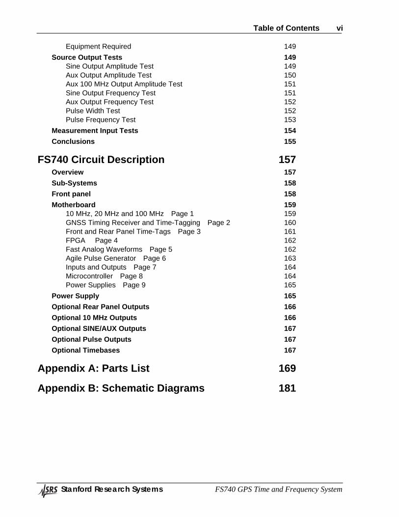
Table of Contents vi
Stanford Research Systems FS740 GPS Time and Frequency System
Equipment Required 149 Source Output Tests 149
Sine Output Amplitude Test 149 Aux Output Amplitude Test 150 Aux 100 MHz Output Amplitude Test 151 Sine Output Frequency Test 151 Aux Output Frequency Test 152 Pulse Width Test 152 Pulse Frequency Test 153
Measurement Input Tests 154 Conclusions 155
FS740 Circuit Description 157
Overview 157 Sub-Systems 158 Front panel 158 Motherboard 159
10 MHz, 20 MHz and 100 MHz Page 1 159 GNSS Timing Receiver and Time-Tagging Page 2 160 Front and Rear Panel Time-Tags Page 3 161 FPGA Page 4 162 Fast Analog Waveforms Page 5 162 Agile Pulse Generator Page 6 163 Inputs and Outputs Page 7 164 Microcontroller Page 8 164 Power Supplies Page 9 165
Power Supply 165 Optional Rear Panel Outputs 166 Optional 10 MHz Outputs 166 Optional SINE/AUX Outputs 167 Optional Pulse Outputs 167 Optional Timebases 167
Appendix A: Parts List 169
Appendix B: Schematic Diagrams 181
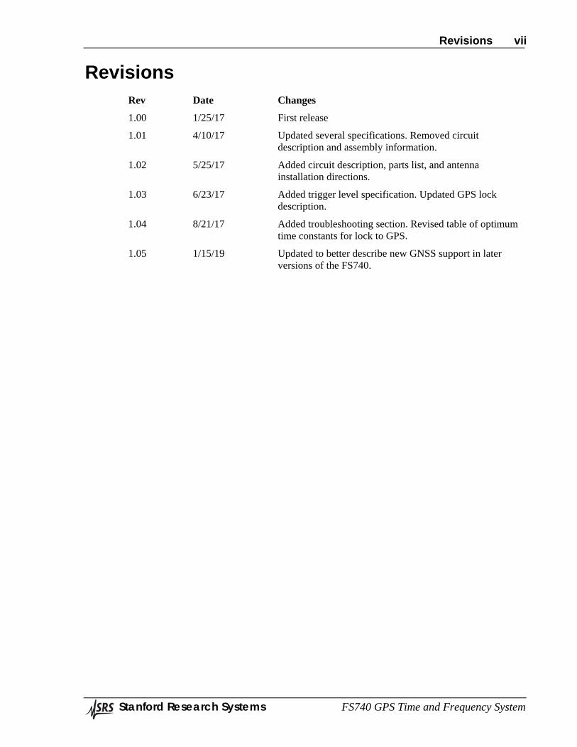
Revisions vii
Stanford Research Systems FS740 GPS Time and Frequency System
Revisions Rev Date Changes
1.00 1/25/17 First release
1.01 4/10/17 Updated several specifications. Removed circuit description and assembly information.
1.02 5/25/17 Added circuit description, parts list, and antenna installation directions.
1.03 6/23/17 Added trigger level specification. Updated GPS lock description.
1.04 8/21/17 Added troubleshooting section. Revised table of optimum time constants for lock to GPS.
1.05 1/15/19 Updated to better describe new GNSS support in later versions of the FS740.

Safety and Preperation for Use ix
Stanford Research Systems FS740 GPS Time and Frequency System
Safety and Preparation for Use Line Voltage The instruments operate from a 90 to 132 VAC or 175 to 264 VAC power source having a line frequency between 47 and 63 Hz. Power consumption is less than 80 VA total. This instrument is intended to be powered at all times. Therefore, there is no power switch. Power is applied to the instrument as soon as the line cord is plugged in.
Power Entry Module A power entry module, labeled AC POWER on the back panel of the instrument, provides connection to the power source and to a protective ground.
Power Cord The unit is shipped with a detachable, three-wire power cord for connection to the power source and protective ground.
The exposed metal parts of the box are connected to the power ground to protect against electrical shock. Always use an outlet which has a properly connected protective ground. Consult with an electrician if necessary.
Grounding BNC shields are connected to the chassis ground and the AC power source ground via the power cord. Do not apply any voltage to the shield.
Line Fuse The line fuse is internal to the instrument and may not be serviced by the user.
Operate Only with Covers in Place To avoid personal injury, do not remove the product covers or panels. Do not operate the product without all covers and panels in place.
Serviceable Parts There are no user serviceable parts. Refer service to a qualified technician.
Safety and Preperation for Use x
Stanford Research Systems FS740 GPS Time and Frequency System
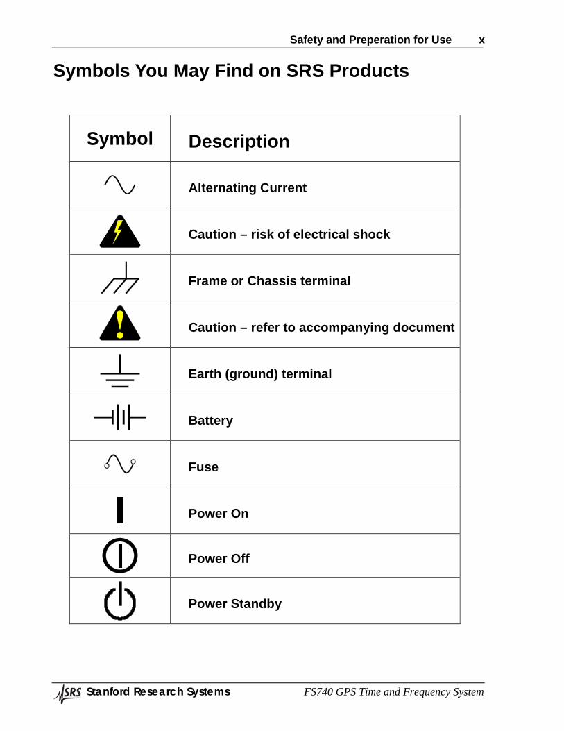
Symbols You May Find on SRS Products
Symbol Description
Alternating Current
Caution – risk of electrical shock
Frame or Chassis terminal
Caution – refer to accompanying document
Earth (ground) terminal
Battery
Fuse
Power On
Power Off
Power Standby
Specifications xi
Stanford Research Systems FS740 GPS Time and Frequency System
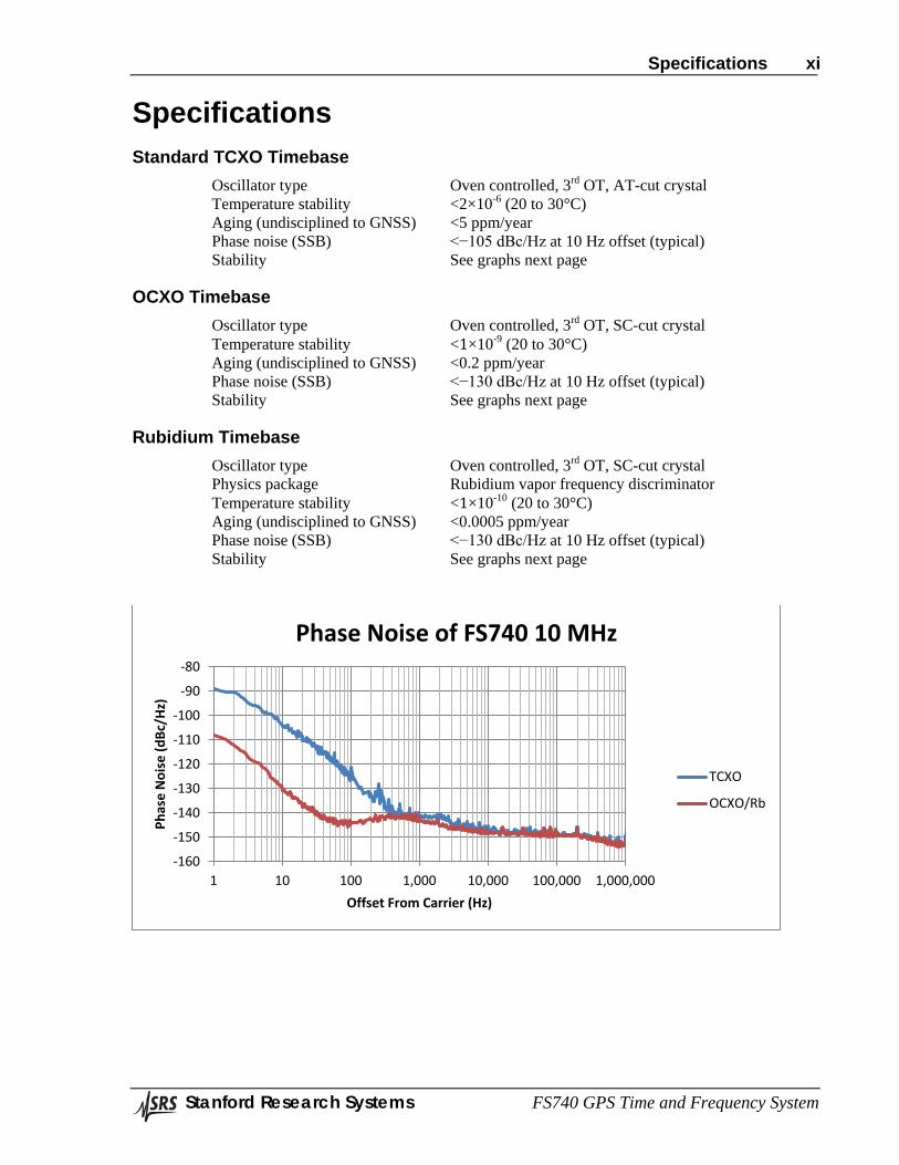
Specifications Standard TCXO Timebase
Oscillator type Oven controlled, 3rd OT, AT-cut crystal Temperature stability <2×10⁻⁶ (20 to 30°C) Aging (undisciplined to GNSS) <5 ppm/year Phase noise (SSB) <−105 dBc/Hz at 10 Hz offset (typical) Stability See graphs next page
OCXO Timebase Oscillator type Oven controlled, 3rd OT, SC-cut crystal Temperature stability <1×10⁻⁹ (20 to 30°C) Aging (undisciplined to GNSS) <0.2 ppm/year Phase noise (SSB) <−130 dBc/Hz at 10 Hz offset (typical) Stability See graphs next page
Rubidium Timebase Oscillator type Oven controlled, 3rd OT, SC-cut crystal Physics package Rubidium vapor frequency discriminator Temperature stability <1×10⁻¹⁰ (20 to 30°C) Aging (undisciplined to GNSS) <0.0005 ppm/year Phase noise (SSB) <−130 dBc/Hz at 10 Hz offset (typical) Stability See graphs next page
-160
-150
-140
-130
-120
-110
-100
-90
-80
1 10 100 1,000 10,000 100,000 1,000,000
Phas
e N
oise
(dBc
/Hz)
Offset From Carrier (Hz)
Phase Noise of FS740 10 MHz
TCXO
OCXO/Rb
Specifications xii
Stanford Research Systems FS740 GPS Time and Frequency System
1E-15
1E-14
1E-13
1E-12
1E-11
1E-10
1E-09
0.01 0.1 1 10 100 1000 10000 100000 1000000
Alla
n De
viat
ion
Time Interval (s)
Typical Frequency Stability for FS740 Locked to GPS
GPS
TCXO
OCXO
Rb
1E-15
1E-14
1E-13
1E-12
1E-11
1E-10
1E-09
0.01 0.1 1 10 100 1000 10000 100000 1000000
Alla
n De
viat
ion
Time Interval (s)
Typical Frequency Stability for FS740 Free Running
GPS
TCXO
OCXO
Rb
Specifications xiii
Stanford Research Systems FS740 GPS Time and Frequency System
GNSS Receiver Model Ublox NEO-M8T Power on to satellite acquistion <1 minute (typical) Time to acquire almanac ~15 minutes when continuously tracking satellites Optimized for static applications Over determined clock mode enables receiver to use all
satellites for timing. Accuracy of UTC < 100 ns Timing wander < 20 ns rms (clear view of the sky) Antenna delay correction range ± 32.767 µs
Sine Output (50 Ω load) Direct DDS generation Frequency range 1 mHz to 30.1 MHz Frequency resolution 1 μHz Frequency error <10 pHz + timebase error × fC Phase settability 1 mDeg Phase accuracy to internal reference <2 ns Amplitude 10 mVPP to 1.414 VPP Amplitude resolution <1 % Amplitude accuracy ±5 % Harmonics <–40 dBc Spurious <–70 dBc Output coupling DC, 50 Ω ±2 % at 10MHz User load 50 Ω Reverse protection ±5 VDC
Aux Output (50 Ω load) Output options: Sine, Triangle, Square, 100MHz, or AM IRIG-B Frequency range Sine 1 mHz to 10 MHz Triangle or square 1 mHz to 1 MHz 100 MHz sine 100 MHz AM IRIG-B 1 kHz Frequency resolution 1 μHz Frequency error <10 pHz + timebase error × fC Phase settability 1 mDeg (cannot adjust phase of 100MHz sine output) Phase accuracy to internal reference <2 ns Amplitude (sine, triangle, square) 10 mVPP to 1.414 VPP
Amplitude (100 MHz) 2.75 dBm ±0.5 dBm Amplitude resolution <1 % Amplitude accuracy ±5 % Harmonics <–40 dBc Spurious <–70 dBc Output coupling DC, 50 Ω ±2 % User load 50 Ω Reverse protection ±5 VDC
Specifications xiv
Stanford Research Systems FS740 GPS Time and Frequency System
Pulse Output Output options: Period/width, Freq/duty, Pulse IRIG-B Period 40 ns to 1000 s Width 5 ns to (Period – 5 ns) Period/width resolution 1 ps Frequency range 1 mHz to 25 MHz Frequency resolution 1 μHz Frequency error <10 pHz + timebase error × fC Phase settability 5 ps Phase accuracy to internal reference <2 ns Jitter <50 ps (rms) Level +5 V CMOS logic Transition time <2 ns Source impedance 50 Ω
10 MHz Output (50 Ω load) Amplitude 13 dBm Amplitude accuracy ±1.5 dBm Harmonics <–50 dBc Spurious <–90 dBc (100 kHz BW) Phase settability Phase can not be adjusted. Output coupling DC, 50 Ω ±2 % User load 50 Ω Reverse protection ±5 VDC
Time and Frequency Input Time tag resolution: 1 ps Time tag jitter (rms) <50 ps Frequency resolution 1 μHz Maximum frequency >120 MHz Measurement stability <10 ps/gate + timebase stability (synchronous)
<100 ps/gate + timebase stability (otherwise) Trigger level ±3 V
Computer Interfaces (standard) Ethernet (LAN) 10/100 Base-T. TCP/IP & DHCP default. RS-232 4.8k-115.2k baud, RTS/CTS flow
Option A: 10 MHz Distribution Number of outputs 5 Specifications Same as motherboard 10MHz output
Option B: Sine/Aux Distribution Number of outputs 5 Specifications Same as motherboard Sine or Aux output
Option C: Pulse Distribution Number of outputs 5 Specifications Same as motherboard Pulse output
Specifications xv
Stanford Research Systems FS740 GPS Time and Frequency System
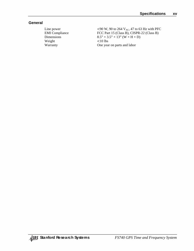
General Line power <90 W, 90 to 264 VAC, 47 to 63 Hz with PFC EMI Compliance FCC Part 15 (Class B), CISPR-22 (Class B) Dimensions 8.5” × 3.5” × 13” (W × H × D) Weight <10 lbs Warranty One year on parts and labor
Commands xvi
Stanford Research Systems FS740 GPS Time and Frequency System
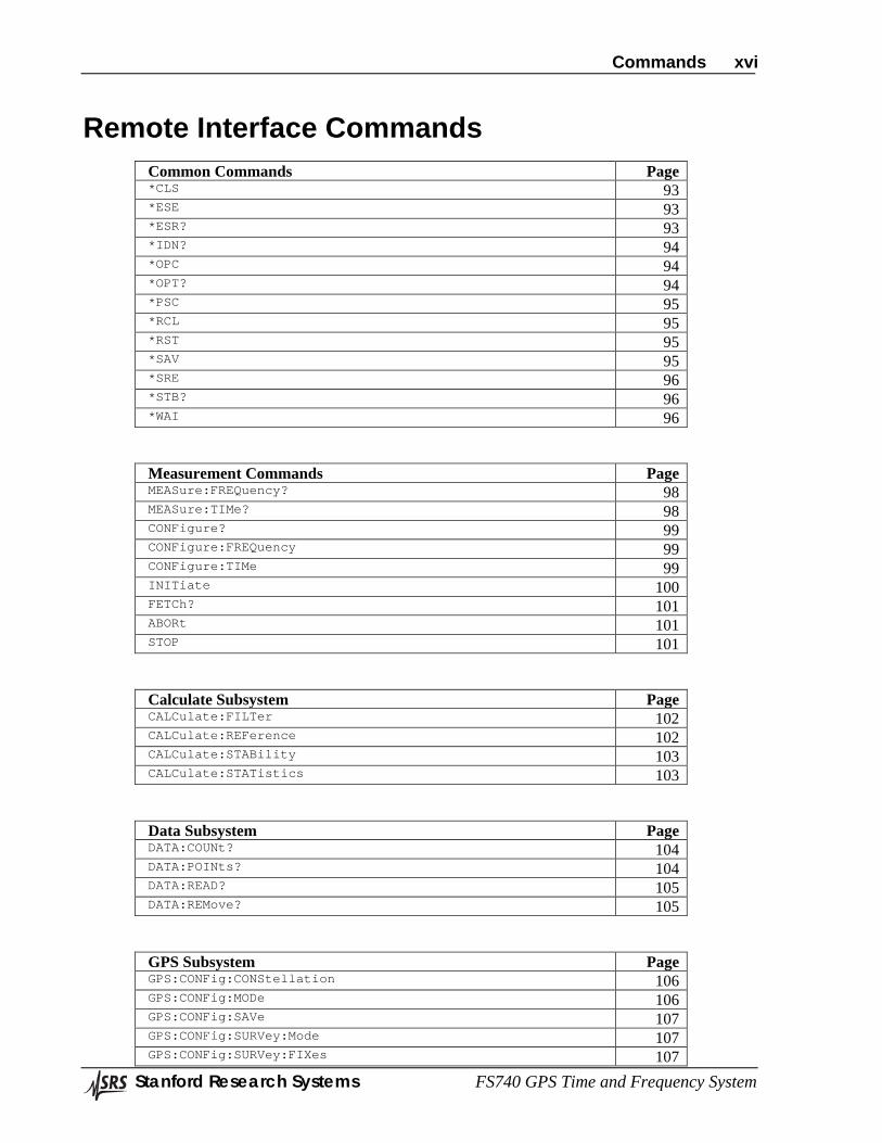
Remote Interface Commands Common Commands Page *CLS 93 *ESE 93 *ESR? 93 *IDN? 94 *OPC 94 *OPT? 94 *PSC 95 *RCL 95 *RST 95 *SAV 95 *SRE 96 *STB? 96 *WAI 96
Measurement Commands Page MEASure:FREQuency? 98 MEASure:TIMe? 98 CONFigure? 99 CONFigure:FREQuency 99 CONFigure:TIMe 99 INITiate 100 FETCh? 101 ABORt 101 STOP 101
Calculate Subsystem Page CALCulate:FILTer 102 CALCulate:REFerence 102 CALCulate:STABility 103 CALCulate:STATistics 103
Data Subsystem Page DATA:COUNt? 104 DATA:POINts? 104 DATA:READ? 105 DATA:REMove? 105
GPS Subsystem Page GPS:CONFig:CONStellation 106 GPS:CONFig:MODe 106 GPS:CONFig:SAVe 107 GPS:CONFig:SURVey:Mode 107 GPS:CONFig:SURVey:FIXes 107
Commands xvii
Stanford Research Systems FS740 GPS Time and Frequency System
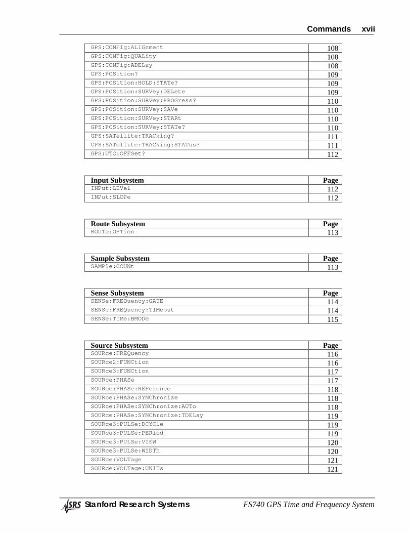
GPS:CONFig:ALIGnment 108 GPS:CONFig:QUALity 108 GPS:CONFig:ADELay 108 GPS:POSition? 109 GPS:POSition:HOLD:STATe? 109 GPS:POSition:SURVey:DELete 109 GPS:POSition:SURVey:PROGress? 110 GPS:POSition:SURVey:SAVe 110 GPS:POSition:SURVey:STARt 110 GPS:POSition:SURVey:STATe? 110 GPS:SATellite:TRACking? 111 GPS:SATellite:TRACking:STATus? 111 GPS:UTC:OFFSet? 112
Input Subsystem Page INPut:LEVel 112 INPut:SLOPe 112
Route Subsystem Page ROUTe:OPTion 113
Sample Subsystem Page SAMPle:COUNt 113
Sense Subsystem Page SENSe:FREQuency:GATE 114 SENSe:FREQuency:TIMeout 114 SENSe:TIMe:BMODe 115
Source Subsystem Page SOURce:FREQuency 116 SOURce2:FUNCtion 116 SOURce3:FUNCtion 117 SOURce:PHASe 117 SOURce:PHASe:REFerence 118 SOURce:PHASe:SYNChronize 118 SOURce:PHASe:SYNChronize:AUTo 118 SOURce:PHASe:SYNChronize:TDELay 119 SOURce3:PULSe:DCYCle 119 SOURce3:PULSe:PERiod 119 SOURce3:PULSe:VIEW 120 SOURce3:PULSe:WIDTh 120 SOURce:VOLTage 121 SOURce:VOLTage:UNITs 121
Commands xviii
Stanford Research Systems FS740 GPS Time and Frequency System
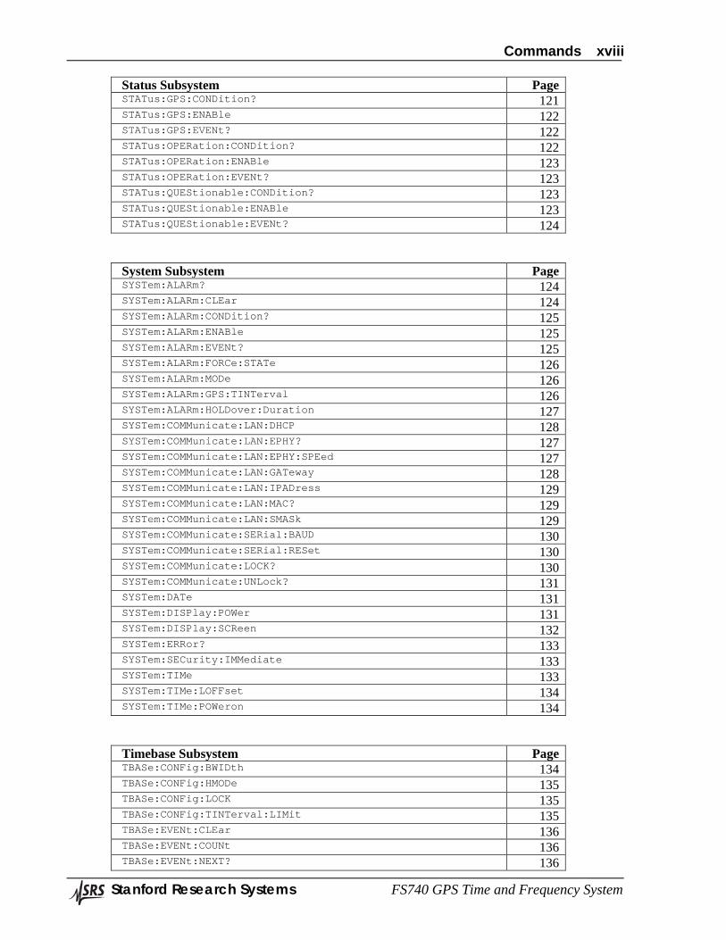
Status Subsystem Page STATus:GPS:CONDition? 121 STATus:GPS:ENABle 122 STATus:GPS:EVENt? 122 STATus:OPERation:CONDition? 122 STATus:OPERation:ENABle 123 STATus:OPERation:EVENt? 123 STATus:QUEStionable:CONDition? 123 STATus:QUEStionable:ENABle 123 STATus:QUEStionable:EVENt? 124
System Subsystem Page SYSTem:ALARm? 124 SYSTem:ALARm:CLEar 124 SYSTem:ALARm:CONDition? 125 SYSTem:ALARm:ENABle 125 SYSTem:ALARm:EVENt? 125 SYSTem:ALARm:FORCe:STATe 126 SYSTem:ALARm:MODe 126 SYSTem:ALARm:GPS:TINTerval 126 SYSTem:ALARm:HOLDover:Duration 127 SYSTem:COMMunicate:LAN:DHCP 128 SYSTem:COMMunicate:LAN:EPHY? 127 SYSTem:COMMunicate:LAN:EPHY:SPEed 127 SYSTem:COMMunicate:LAN:GATeway 128 SYSTem:COMMunicate:LAN:IPADress 129 SYSTem:COMMunicate:LAN:MAC? 129 SYSTem:COMMunicate:LAN:SMASk 129 SYSTem:COMMunicate:SERial:BAUD 130 SYSTem:COMMunicate:SERial:RESet 130 SYSTem:COMMunicate:LOCK? 130 SYSTem:COMMunicate:UNLock? 131 SYSTem:DATe 131 SYSTem:DISPlay:POWer 131 SYSTem:DISPlay:SCReen 132 SYSTem:ERRor? 133 SYSTem:SECurity:IMMediate 133 SYSTem:TIMe 133 SYSTem:TIMe:LOFFset 134 SYSTem:TIMe:POWeron 134
Timebase Subsystem Page TBASe:CONFig:BWIDth 134 TBASe:CONFig:HMODe 135 TBASe:CONFig:LOCK 135 TBASe:CONFig:TINTerval:LIMit 135 TBASe:EVENt:CLEar 136 TBASe:EVENt:COUNt 136 TBASe:EVENt:NEXT? 136
Commands xix
Stanford Research Systems FS740 GPS Time and Frequency System
TBASe:FCONtrol 137 TBASe:FCONtrol:SAVe 137 TBASe:STATe? 138 TBASe:STATe:HOLDover:DURation? 138 TBASe:STATe:LOCK:DURation? 138 TBASe:STATe:WARMup:DURation? 139 TBASe:TCONstant 139 TBASe:TINTerval 139
Trigger Subsystem Page TRIGger:CONTinuous 140

Quick Start Instructions 1
Stanford Research Systems FS740 GPS Time and Frequency System
Quick Start Instructions
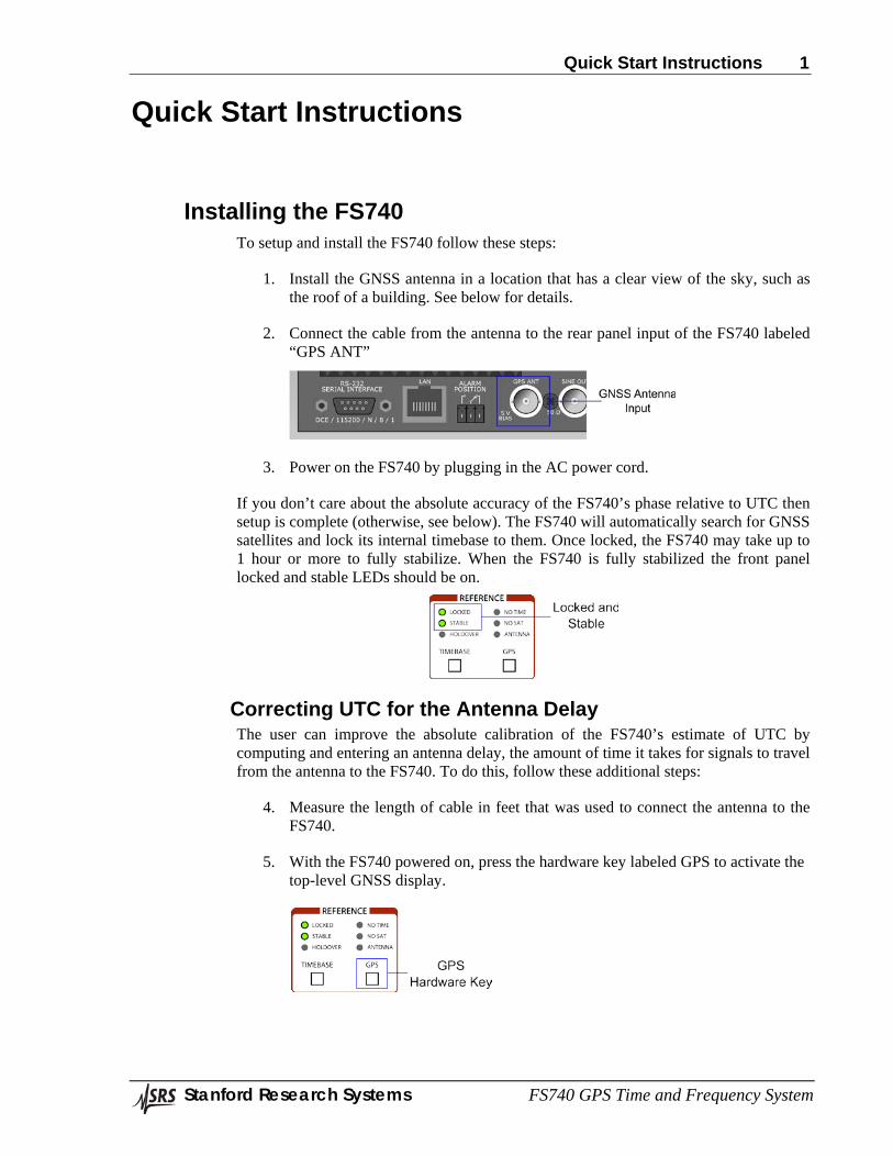
Installing the FS740 To setup and install the FS740 follow these steps:
1. Install the GNSS antenna in a location that has a clear view of the sky, such as the roof of a building. See below for details.
2. Connect the cable from the antenna to the rear panel input of the FS740 labeled “GPS ANT”
3. Power on the FS740 by plugging in the AC power cord.
If you don’t care about the absolute accuracy of the FS740’s phase relative to UTC then setup is complete (otherwise, see below). The FS740 will automatically search for GNSS satellites and lock its internal timebase to them. Once locked, the FS740 may take up to 1 hour or more to fully stabilize. When the FS740 is fully stabilized the front panel locked and stable LEDs should be on.
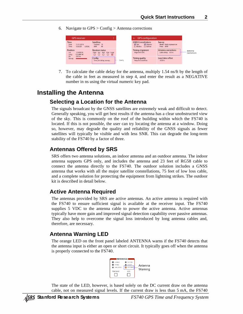
Correcting UTC for the Antenna Delay The user can improve the absolute calibration of the FS740’s estimate of UTC by computing and entering an antenna delay, the amount of time it takes for signals to travel from the antenna to the FS740. To do this, follow these additional steps:
4. Measure the length of cable in feet that was used to connect the antenna to the FS740.
5. With the FS740 powered on, press the hardware key labeled GPS to activate the top-level GNSS display.
Quick Start Instructions 2
Stanford Research Systems FS740 GPS Time and Frequency System
6. Navigate to GPS > Config > Antenna corrections
7. To calculate the cable delay for the antenna, multiply 1.54 ns/ft by the length of the cable in feet as measured in step 4, and enter the result as a NEGATIVE number in ns using the virtual numeric key pad.
Installing the Antenna Selecting a Location for the Antenna
The signals broadcast by the GNSS satellites are extremely weak and difficult to detect. Generally speaking, you will get best results if the antenna has a clear unobstructed view of the sky. This is commonly on the roof of the building within which the FS740 is located. If this is not possible, the user can try locating the antenna at a window. Doing so, however, may degrade the quality and reliability of the GNSS signals as fewer satellites will typically be visible and with less SNR. This can degrade the long-term stability of the FS740 by a factor of three.
Antennas Offered by SRS SRS offers two antenna solutions, an indoor antenna and an outdoor antenna. The indoor antenna supports GPS only, and includes the antenna and 23 feet of RG58 cable to connect the antenna directly to the FS740. The outdoor solution includes a GNSS antenna that works with all the major satellite constellations, 75 feet of low loss cable, and a complete solution for protecting the equipment from lightning strikes. The outdoor kit is described in detail below.
Active Antenna Required The antennas provided by SRS are active antennas. An active antenna is required with the FS740 to ensure sufficient signal is available at the receiver input. The FS740 supplies 5 VDC to the antenna cable to power the active antenna. Active antennas typically have more gain and improved signal detection capability over passive antennas. They also help to overcome the signal loss introduced by long antenna cables and, therefore, are necessary.
Antenna Warning LED The orange LED on the front panel labeled ANTENNA warns if the FS740 detects that the antenna input is either an open or short circuit. It typically goes off when the antenna is properly connected to the FS740.
The state of the LED, however, is based solely on the DC current draw on the antenna cable, not on measured signal levels. If the current draw is less than 5 mA, the FS740
Quick Start Instructions 3
Stanford Research Systems FS740 GPS Time and Frequency System
will warn of an open circuit. If the current draw is greater than 75 mA, the FS740 will warn of a short circuit. The total current draw for the antenna is limited to 300 mA. Please note that the performance of the FS740 is not impacted at all if the power draw of your antenna falls outside this range, The FS740’s GNSS receiver will continuously search for GNSS satellites regardless of the current draw on the antenna. The warning LED is merely meant to be a helpful diagnostic to consider when troubleshooting a lack of signal for the most common installations.
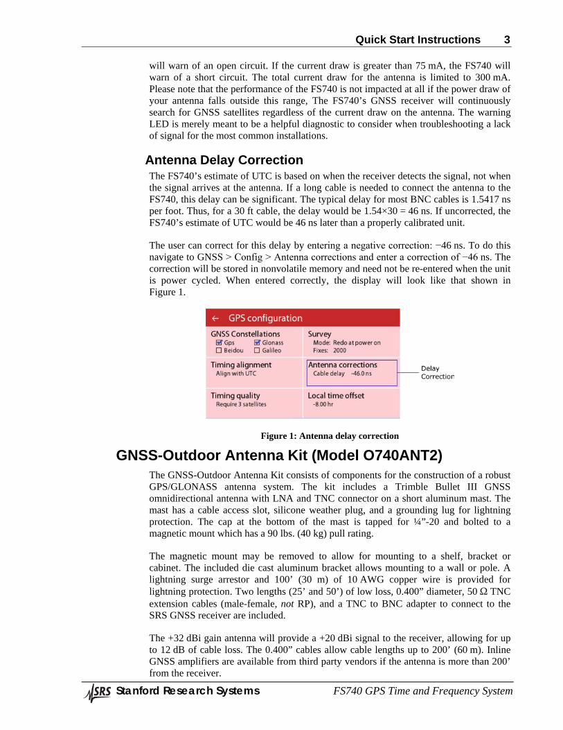
Antenna Delay Correction The FS740’s estimate of UTC is based on when the receiver detects the signal, not when the signal arrives at the antenna. If a long cable is needed to connect the antenna to the FS740, this delay can be significant. The typical delay for most BNC cables is 1.5417 ns per foot. Thus, for a 30 ft cable, the delay would be 1.54×30 = 46 ns. If uncorrected, the FS740’s estimate of UTC would be 46 ns later than a properly calibrated unit.
The user can correct for this delay by entering a negative correction: −46 ns. To do this navigate to GNSS > Config > Antenna corrections and enter a correction of −46 ns. The correction will be stored in nonvolatile memory and need not be re-entered when the unit is power cycled. When entered correctly, the display will look like that shown in Figure 1.
Figure 1: Antenna delay correction
GNSS-Outdoor Antenna Kit (Model O740ANT2) The GNSS-Outdoor Antenna Kit consists of components for the construction of a robust GPS/GLONASS antenna system. The kit includes a Trimble Bullet III GNSS omnidirectional antenna with LNA and TNC connector on a short aluminum mast. The mast has a cable access slot, silicone weather plug, and a grounding lug for lightning protection. The cap at the bottom of the mast is tapped for ¼”-20 and bolted to a magnetic mount which has a 90 lbs. (40 kg) pull rating.
The magnetic mount may be removed to allow for mounting to a shelf, bracket or cabinet. The included die cast aluminum bracket allows mounting to a wall or pole. A lightning surge arrestor and 100’ (30 m) of 10 AWG copper wire is provided for lightning protection. Two lengths (25’ and 50’) of low loss, 0.400” diameter, 50 Ω TNC extension cables (male-female, not RP), and a TNC to BNC adapter to connect to the SRS GNSS receiver are included.
The +32 dBi gain antenna will provide a +20 dBi signal to the receiver, allowing for up to 12 dB of cable loss. The 0.400” cables allow cable lengths up to 200’ (60 m). Inline GNSS amplifiers are available from third party vendors if the antenna is more than 200’ from the receiver.
Quick Start Instructions 4
Stanford Research Systems FS740 GPS Time and Frequency System
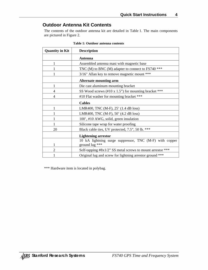
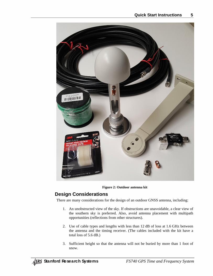
Outdoor Antenna Kit Contents The contents of the outdoor antenna kit are detailed in Table 1. The main components are pictured in Figure 2.
Table 1: Outdoor antenna contents
Quantity in Kit Description
Antenna 1 Assembled antenna mast with magnetic base 1 TNC (M) to BNC (M) adapter to connect to FS740 *** 1 3/16" Allan key to remove magnetic mount ***
Alternate mounting arm 1 Die cast aluminum mounting bracket 4 SS Wood screws (#10 x 1.5”) for mounting bracket *** 4 #10 Flat washer for mounting bracket ***
Cables 1 LMR400, TNC (M-F), 25’ (1.4 dB loss) 1 LMR400, TNC (M-F), 50’ (4.2 dB loss) 1 100’, #10 AWG, solid, green insulation 1 Silicone tape wrap for water proofing 20 Black cable ties, UV protected, 7.5”, 50 lb. ***
Lightening arrestor
1 10 kA lightning surge suppressor, TNC (M-F) with copper ground lug ***
2 Self-tapping #8x1/2” SS metal screws to mount arrestor *** 1 Original lug and screw for lightning arrestor ground ***
*** Hardware item is located in polybag.
Quick Start Instructions 5
Stanford Research Systems FS740 GPS Time and Frequency System
Figure 2: Outdoor antenna kit
Design Considerations There are many considerations for the design of an outdoor GNSS antenna, including:
1. An unobstructed view of the sky. If obstructions are unavoidable, a clear view of the southern sky is preferred. Also, avoid antenna placement with multipath opportunities (reflections from other structures).
2. Use of cable types and lengths with less than 12 dB of loss at 1.6 GHz between the antenna and the timing receiver. (The cables included with the kit have a total loss of 5.6 dB.)
3. Sufficient height so that the antenna will not be buried by more than 1 foot of snow.
Quick Start Instructions 6
Stanford Research Systems FS740 GPS Time and Frequency System
4. Strategies to avoid lightning strikes. Avoid being the highest metal object (which, unfortunately, conflicts with a clear sky view and avoiding multipath).
5. A strategy to handle a lightning strike. This is a complicated and important topic which must be addressed to insure the safety of personnel and reduce equipment damage. The antenna mast and inline lightning surge arrestor, included with the antenna kit, must be attached to a grounded structure, or connected to earth ground via a grounding rod.
6. Compliance with local building and electrical codes.
7. Compliance with building lease term and easements.
When designing the outdoor GNSS antenna system, site specific designs and the use of other materials will be required. If additional cables are needed they should have a TNC male on one end and a TNC female connector on the other, so that they may be used as extension cables without coax barrels. These are not RP cables (which reverse the pin and socket of conventional connectors). The cables sold by SRS are not plenum rated. For additional TNC cables we suggest part number 28-463-050 (a 50’ cable with a typical loss of 4.2 dB) available from http://www.showmecables.com/
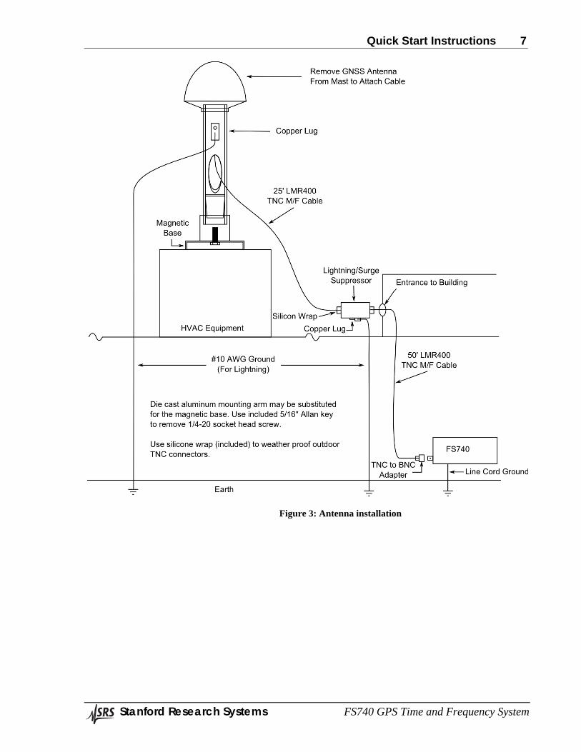
Mounting the Antenna The required connections for installing the antenna are highlighted in Figure 3. The simplest semi-permanent installation uses the magnetic antenna mount placed on top of a HVAC unit on the roof. If HVAC placement is not available, the magnetic mount can be attached to a 10 lbs. weight (barbell weights work well for this purpose) and placed on the roof.
Alternatively, the magnetic mount can be removed allowing the antenna to mount to a wall or pole using the included mounting arm. The antenna may also be mounted to any horizontal surface or brace which has a ¼” diameter hole. A 3/16” hex wrench is included in the kit to remove the magnetic mount from the antenna mast. The hardware, including fiber washers to break galvanic contact, should be reused.
To connect the antenna to the coax cable, first remove the antenna from the mast. Observing the gender of both ends of the cable, thread the male end of the cable through the oval slot in the antenna mast. Remove the plastic protector from the antenna connector. Screw the cable on to the antenna connector finger tight. Push the cable down into the mast and screw the antenna onto the mast. (The TNC connector is free to rotate, and the direction of rotation will not cause the TNC to loosen.)
Lightning Protection There are two important components for lightning protection: A ground wire attached directly to the aluminum antenna mast, and a lightning arrestor/surge absorber located where the coax cable enters the building. The arrestor has a TNC male connector on one end and a TNC female on the other and a lug for earth ground in the center. Both the antenna mast ground and the lightning arrestor must be separately connected to earth ground with #10 AWG copper wire (included with kit). All outdoor TNC connectors, including those attached to the lightning arrestor, should be protected from weather and sunlight exposure with the included silicone tape wrap.
Quick Start Instructions 7
Stanford Research Systems FS740 GPS Time and Frequency System
Figure 3: Antenna installation
Quick Start Instructions 8
Stanford Research Systems FS740 GPS Time and Frequency System
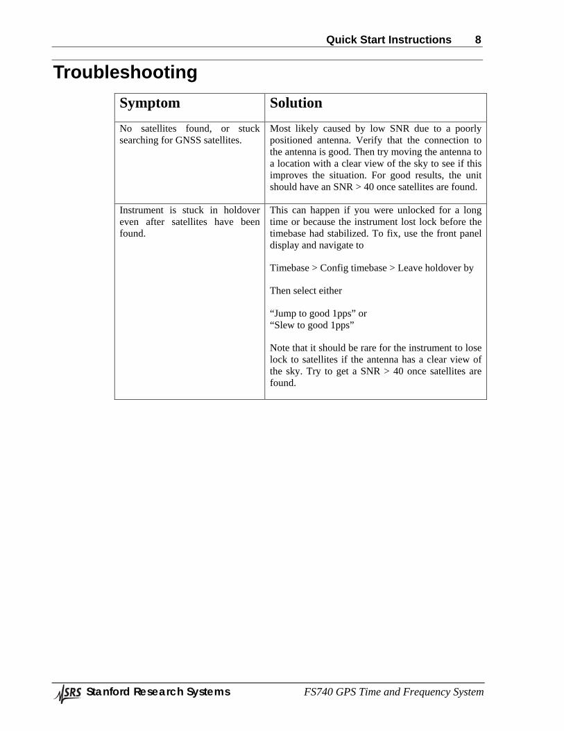
Troubleshooting Symptom Solution No satellites found, or stuck searching for GNSS satellites.
Most likely caused by low SNR due to a poorly positioned antenna. Verify that the connection to the antenna is good. Then try moving the antenna to a location with a clear view of the sky to see if this improves the situation. For good results, the unit should have an SNR > 40 once satellites are found.
Instrument is stuck in holdover even after satellites have been found.
This can happen if you were unlocked for a long time or because the instrument lost lock before the timebase had stabilized. To fix, use the front panel display and navigate to
Timebase > Config timebase > Leave holdover by
Then select either
“Jump to good 1pps” or “Slew to good 1pps”
Note that it should be rare for the instrument to lose lock to satellites if the antenna has a clear view of the sky. Try to get a SNR > 40 once satellites are found.
Introduction 9
Stanford Research Systems FS740 GPS Time and Frequency System
Introduction
Feature Overview The FS740 GPS Time and Frequency System is primarily designed to provide continuously calibrated time and frequency distribution to a local laboratory. Calibration is maintained by locking its internal reference to the time of day signals broadcast by the GNSS satellites. The satellites which make up the various GNSS networks are equipped with rubidium and cesium clocks which are monitored and controlled by government agencies, such as the U.S. Air Force for GPS, which steer the timing of the GNSS satellites to maintain synchronicity with UTC. The FS740 includes a GNSS receiver that is specifically designed to generate precise timing. When locked to GNSS satellites, the FS740 can align its outputs and time tag signals on its inputs to UTC with a relative precision of 5 ps, an RMS deviation of less than 20 ns and an absolute accuracy of 100 ns.
On its front panel, the FS740 provides three user configurable outputs: a sine output, an aux output, and a pulse output. The sine output supports the generation of frequencies from 1 mHz to 30.1 MHz and amplitudes ranging from 10 mVPP to 1.414 VPP. Its phase can be adjusted with 1 millidegree of relative precision. Furthermore, if the FS740 is locked to GNSS satellites, the zero crossings of the output can be synchronized to UTC if desired.
The aux output supports the generation of several different signals: sine waves, triangle waves, zero-centered square waves, a fixed 100 MHz sine wave, and an AM modulated IRIG-B timing code. Frequencies up to 10 MHz are supported for sine waves, and up to 1 MHz for triangle and square waves. Like the sine output, amplitudes for these three signals may range from 10 mVPP to 1.414 VPP. Its phase can be adjusted with 1 millidegree of relative precision, and synchronized to UTC if desired. The 100 MHz sine output has a fixed amplitude (2.75 dBm) and frequency and is intended for synchronization of high frequency equipment. Finally, the IRIG-B signal may be used for time of day distribution
The pulse output generates 5 V CMOS waveforms with frequencies ranging from 1 mHz to 25 MHz, and pulse widths ranging from 5 ns to the period – 5 ns. The user may specify a period and pulse width, or a frequency and duty cycle. Periods and pulse width may be specified with 1 ps of resolution. Frequencies may be specified with 1 uHz resolution. The phase of the pulses can be adjusted with 5 ps of resolution. If the FS740 is locked to GNSS satellites, the rising edge of the pulse output can be synchronized to UTC if desired. Finally, the pulse output can also be configured to generate pulse-width-modulated IRIG-B timing codes for time of day distribution.
For expanded distribution, the FS740 comes standard with copies of the three front panel outputs as well as a 10 MHz output on its rear panel. Any of these outputs, including the 10 MHz output, can be expanded with up to 15 more buffered outputs with the installation of up to three option boards on the rear panel, thereby providing ample distribution capability for a local laboratory.
In addition to distributing time and frequency signals to other instrumentation, the FS740 also includes the ability to measure time and frequency of external signals. It can time tag an event relative to UTC with less than 50 ps of jitter. Alternatively, it can measure frequencies of up to 120 MHz with gates ranging from 10 ms to 1000 s, providing up to 12 digits of resolution in a 1 second gate interval. Two measurement inputs are available to the user: one on the front panel and one on the rear panel. Both inputs may be operated independently, and simultaneously.
Introduction 10
Stanford Research Systems FS740 GPS Time and Frequency System
Finally, the FS740 is ideally suited to making frequency stability measurements. It generates averaged time tags at 10 ms intervals with no dead time enabling it to compute Allan deviation stability results for intervals from 10 ms to 50 million seconds automatically. Measurements can be easily configured from the front panel and results viewed in real time without an external computer. Long term stability measurements can be initiated and left to run autonomously for months at time if desired. Results may be periodically downloaded while the measurement continues to run.
Introduction 11
Stanford Research Systems FS740 GPS Time and Frequency System
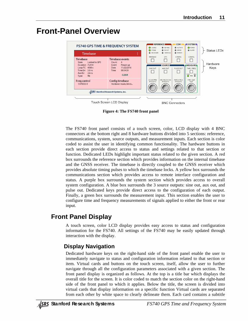
Front-Panel Overview
Figure 4: The FS740 front panel
The FS740 front panel consists of a touch screen, color, LCD display with 4 BNC connectors at the bottom right and 8 hardware buttons divided into 5 sections: reference, communications, system, source outputs, and measurement inputs. Each section is color coded to assist the user in identifying common functionality. The hardware buttons in each section provide direct access to status and settings related to that section or function. Dedicated LEDs highlight important status related to the given section. A red box surrounds the reference section which provides information on the internal timebase and the GNSS receiver. The timebase is directly coupled to the GNSS receiver which provides absolute timing pulses to which the timebase locks. A yellow box surrounds the communications section which provides access to remote interface configuration and status. A purple box surrounds the system section which provides access to overall system configuration. A blue box surrounds the 3 source outputs: sine out, aux out, and pulse out. Dedicated keys provide direct access to the configuration of each output. Finally, a green box surrounds the measurement input. This section enables the user to configure time and frequency measurements of signals applied to either the front or rear input.
Front Panel Display A touch screen, color LCD display provides easy access to status and configuration information for the FS740. All settings of the FS740 may be easily updated through interaction with the display.
Display Navigation Dedicated hardware keys on the right-hand side of the front panel enable the user to immediately navigate to status and configuration information related to that section or item. Virtual cards and buttons on the touch screen, itself, allow the user to further navigate through all the configuration parameters associated with a given section. The front panel display is organized as follows. At the top is a title bar which displays the overall title for the screen. It is color coded to match the section color on the right-hand side of the front panel to which it applies. Below the title, the screen is divided into virtual cards that display information on a specific function Virtual cards are separated from each other by white space to clearly delineate them. Each card contains a subtitle
Introduction 12
Stanford Research Systems FS740 GPS Time and Frequency System
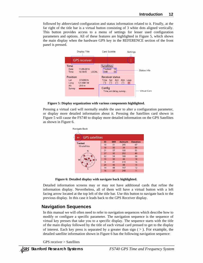
followed by abbreviated configuration and status information related to it. Finally, at the far right of the title bar is a virtual button consisting of 3 white dots aligned vertically. This button provides access to a menu of settings for lesser used configuration parameters and options. All of these features are highlighted in Figure 5, which shows the main display when the hardware GPS key in the REFERENCE section of the front panel is pressed.
Figure 5: Display organization with various components highlighted.
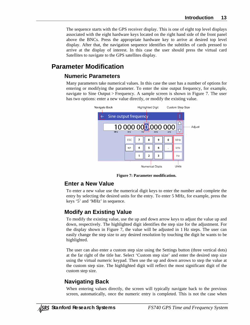
Pressing a virtual card will normally enable the user to alter a configuration parameter, or display more detailed information about it. Pressing the Satellites card shown in Figure 5 will cause the FS740 to display more detailed information on the GPS Satellites as shown in Figure 6.
Figure 6: Detailed display with navigate back highlighted.
Detailed information screens may or may not have additional cards that refine the information display. Nevertheless, all of them will have a virtual button with a left facing arrow located at the top left of the title bar. Use this button to navigate back to the previous display. In this case it leads back to the GPS Receiver display.
Navigation Sequences In this manual we will often need to refer to navigation sequences which describe how to modify or configure a specific parameter. The navigation sequence is the sequence of virtual key presses that take you to a specific display. The sequence starts with the title of the main display followed by the title of each virtual card pressed to get to the display of interest. Each key press is separated by a greater than sign ( > ). For example, the detailed satellite information shown in Figure 6 has the following navigation sequence:
GPS receiver > Satellites
Introduction 13
Stanford Research Systems FS740 GPS Time and Frequency System
The sequence starts with the GPS receiver display. This is one of eight top level displays associated with the eight hardware keys located on the right hand side of the front panel above the BNCs. Press the appropriate hardware key to arrive at desired top level display. After that, the navigation sequence identifies the subtitles of cards pressed to arrive at the display of interest. In this case the user should press the virtual card Satellites to navigate to the GPS satellites display.
Parameter Modification Numeric Parameters
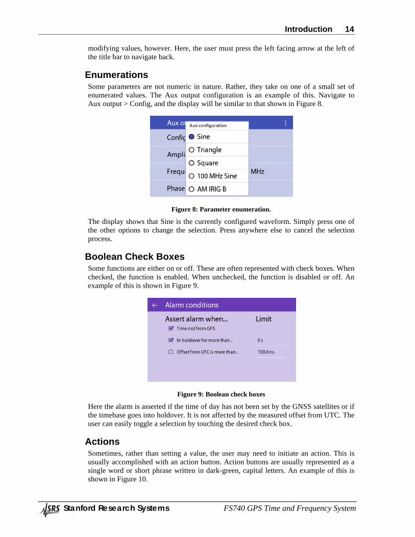
Many parameters take numerical values. In this case the user has a number of options for entering or modifying the parameter. To enter the sine output frequency, for example, navigate to Sine Output > Frequency. A sample screen is shown in Figure 7. The user has two options: enter a new value directly, or modify the existing value.
Figure 7: Parameter modification.
Enter a New Value To enter a new value use the numerical digit keys to enter the number and complete the entry by selecting the desired units for the entry. To enter 5 MHz, for example, press the keys ‘5’ and ‘MHz’ in sequence.
Modify an Existing Value To modify the existing value, use the up and down arrow keys to adjust the value up and down, respectively. The highlighted digit identifies the step size for the adjustment. For the display shown in Figure 7, the value will be adjusted in 1 Hz steps. The user can easily change the step size to any desired resolution by touching the digit he wants to be highlighted.
The user can also enter a custom step size using the Settings button (three vertical dots) at the far right of the title bar. Select ‘Custom step size’ and enter the desired step size using the virtual numeric keypad. Then use the up and down arrows to step the value at the custom step size. The highlighted digit will reflect the most significant digit of the custom step size.
Navigating Back When entering values directly, the screen will typically navigate back to the previous screen, automatically, once the numeric entry is completed. This is not the case when
Introduction 14
Stanford Research Systems FS740 GPS Time and Frequency System
modifying values, however. Here, the user must press the left facing arrow at the left of the title bar to navigate back.
Enumerations Some parameters are not numeric in nature. Rather, they take on one of a small set of enumerated values. The Aux output configuration is an example of this. Navigate to Aux output > Config, and the display will be similar to that shown in Figure 8.
Figure 8: Parameter enumeration.
The display shows that Sine is the currently configured waveform. Simply press one of the other options to change the selection. Press anywhere else to cancel the selection process.
Boolean Check Boxes Some functions are either on or off. These are often represented with check boxes. When checked, the function is enabled. When unchecked, the function is disabled or off. An example of this is shown in Figure 9.
Figure 9: Boolean check boxes
Here the alarm is asserted if the time of day has not been set by the GNSS satellites or if the timebase goes into holdover. It is not affected by the measured offset from UTC. The user can easily toggle a selection by touching the desired check box.
Actions Sometimes, rather than setting a value, the user may need to initiate an action. This is usually accomplished with an action button. Action buttons are usually represented as a single word or short phrase written in dark-green, capital letters. An example of this is shown in Figure 10.
Introduction 15
Stanford Research Systems FS740 GPS Time and Frequency System
Figure 10: Action button
Here, pressing the RESTART button would restart the position survey, which is currently 20% complete.
Top Level Displays and Buttons On the right hand side of the front panel, above the 4 BNCs, are 8 physical buttons identified as hardware keys in Figure 4. Each button is associated with a top level display that enables the user to view status and configuration information for a given area of functionality.
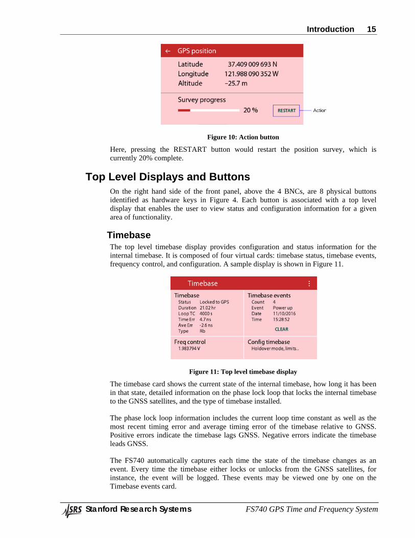
Timebase The top level timebase display provides configuration and status information for the internal timebase. It is composed of four virtual cards: timebase status, timebase events, frequency control, and configuration. A sample display is shown in Figure 11.
Figure 11: Top level timebase display
The timebase card shows the current state of the internal timebase, how long it has been in that state, detailed information on the phase lock loop that locks the internal timebase to the GNSS satellites, and the type of timebase installed.
The phase lock loop information includes the current loop time constant as well as the most recent timing error and average timing error of the timebase relative to GNSS. Positive errors indicate the timebase lags GNSS. Negative errors indicate the timebase leads GNSS.
The FS740 automatically captures each time the state of the timebase changes as an event. Every time the timebase either locks or unlocks from the GNSS satellites, for instance, the event will be logged. These events may be viewed one by one on the Timebase events card.
Introduction 16
Stanford Research Systems FS740 GPS Time and Frequency System
The frequency control voltage is the voltage applied to the frequency input of the timebase to maintain lock to GPS. It is updated every second when the receiver is generating timing pulses. When the timebase is locked to GPS, the frequency control value cannot be changed by the user. If the timebase is not locked to GPS, the user may change the frequency of the timebase by updating this voltage.
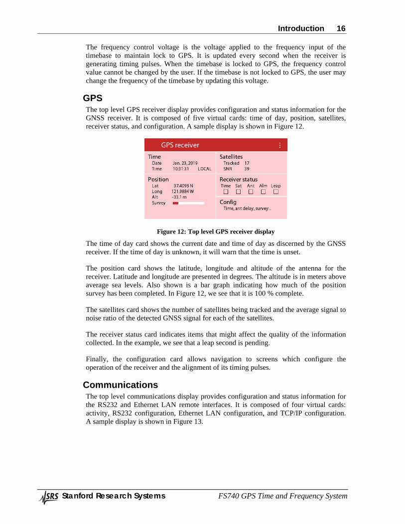
GPS The top level GPS receiver display provides configuration and status information for the GNSS receiver. It is composed of five virtual cards: time of day, position, satellites, receiver status, and configuration. A sample display is shown in Figure 12.
Figure 12: Top level GPS receiver display
The time of day card shows the current date and time of day as discerned by the GNSS receiver. If the time of day is unknown, it will warn that the time is unset.
The position card shows the latitude, longitude and altitude of the antenna for the receiver. Latitude and longitude are presented in degrees. The altitude is in meters above average sea levels. Also shown is a bar graph indicating how much of the position survey has been completed. In Figure 12, we see that it is 100 % complete.
The satellites card shows the number of satellites being tracked and the average signal to noise ratio of the detected GNSS signal for each of the satellites.
The receiver status card indicates items that might affect the quality of the information collected. In the example, we see that a leap second is pending.
Finally, the configuration card allows navigation to screens which configure the operation of the receiver and the alignment of its timing pulses.
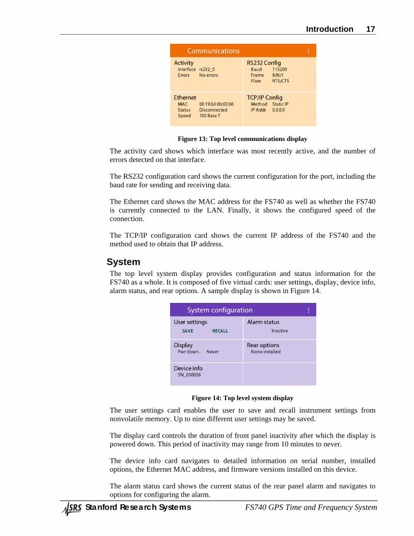
Communications The top level communications display provides configuration and status information for the RS232 and Ethernet LAN remote interfaces. It is composed of four virtual cards: activity, RS232 configuration, Ethernet LAN configuration, and TCP/IP configuration. A sample display is shown in Figure 13.
Introduction 17
Stanford Research Systems FS740 GPS Time and Frequency System
Figure 13: Top level communications display
The activity card shows which interface was most recently active, and the number of errors detected on that interface.
The RS232 configuration card shows the current configuration for the port, including the baud rate for sending and receiving data.
The Ethernet card shows the MAC address for the FS740 as well as whether the FS740 is currently connected to the LAN. Finally, it shows the configured speed of the connection.
The TCP/IP configuration card shows the current IP address of the FS740 and the method used to obtain that IP address.
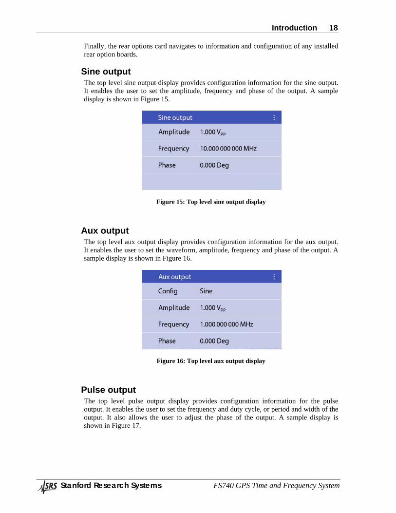
System The top level system display provides configuration and status information for the FS740 as a whole. It is composed of five virtual cards: user settings, display, device info, alarm status, and rear options. A sample display is shown in Figure 14.
Figure 14: Top level system display
The user settings card enables the user to save and recall instrument settings from nonvolatile memory. Up to nine different user settings may be saved.
The display card controls the duration of front panel inactivity after which the display is powered down. This period of inactivity may range from 10 minutes to never.
The device info card navigates to detailed information on serial number, installed options, the Ethernet MAC address, and firmware versions installed on this device.
The alarm status card shows the current status of the rear panel alarm and navigates to options for configuring the alarm.
Introduction 18
Stanford Research Systems FS740 GPS Time and Frequency System
Finally, the rear options card navigates to information and configuration of any installed rear option boards.
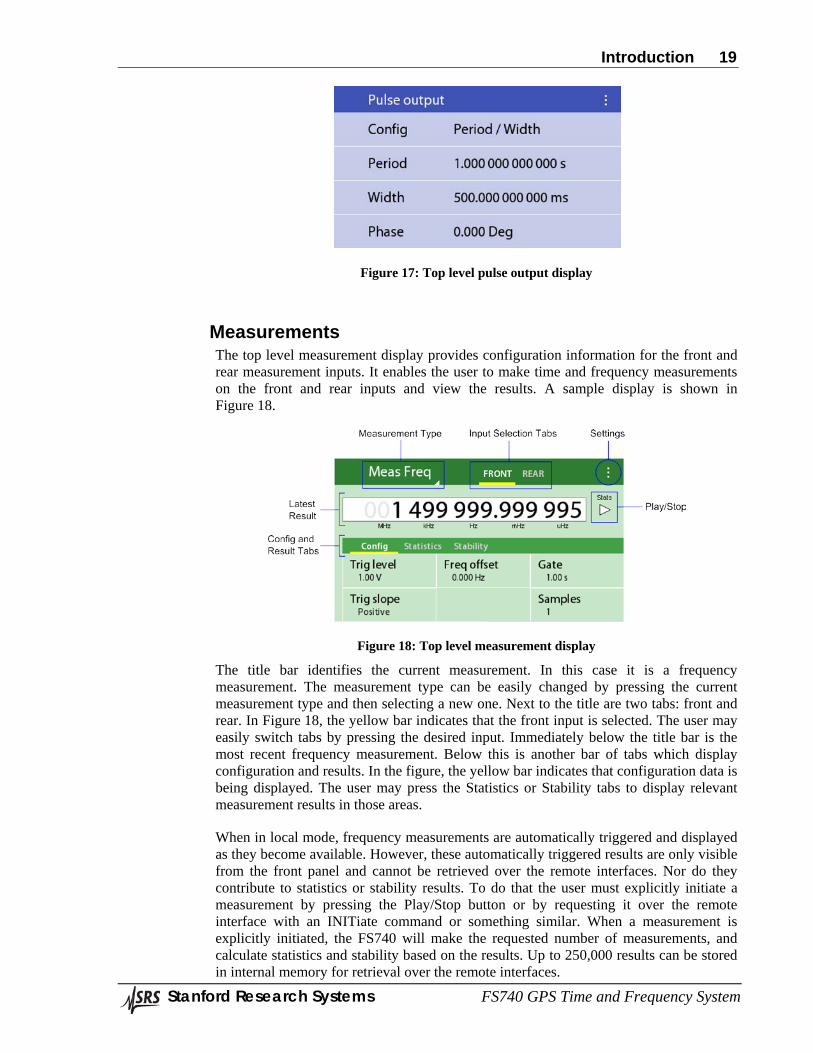
Sine output The top level sine output display provides configuration information for the sine output. It enables the user to set the amplitude, frequency and phase of the output. A sample display is shown in Figure 15.
Figure 15: Top level sine output display
Aux output The top level aux output display provides configuration information for the aux output. It enables the user to set the waveform, amplitude, frequency and phase of the output. A sample display is shown in Figure 16.
Figure 16: Top level aux output display
Pulse output The top level pulse output display provides configuration information for the pulse output. It enables the user to set the frequency and duty cycle, or period and width of the output. It also allows the user to adjust the phase of the output. A sample display is shown in Figure 17.
Introduction 19
Stanford Research Systems FS740 GPS Time and Frequency System
Figure 17: Top level pulse output display
Measurements The top level measurement display provides configuration information for the front and rear measurement inputs. It enables the user to make time and frequency measurements on the front and rear inputs and view the results. A sample display is shown in Figure 18.
Figure 18: Top level measurement display
The title bar identifies the current measurement. In this case it is a frequency measurement. The measurement type can be easily changed by pressing the current measurement type and then selecting a new one. Next to the title are two tabs: front and rear. In Figure 18, the yellow bar indicates that the front input is selected. The user may easily switch tabs by pressing the desired input. Immediately below the title bar is the most recent frequency measurement. Below this is another bar of tabs which display configuration and results. In the figure, the yellow bar indicates that configuration data is being displayed. The user may press the Statistics or Stability tabs to display relevant measurement results in those areas.
When in local mode, frequency measurements are automatically triggered and displayed as they become available. However, these automatically triggered results are only visible from the front panel and cannot be retrieved over the remote interfaces. Nor do they contribute to statistics or stability results. To do that the user must explicitly initiate a measurement by pressing the Play/Stop button or by requesting it over the remote interface with an INITiate command or something similar. When a measurement is explicitly initiated, the FS740 will make the requested number of measurements, and calculate statistics and stability based on the results. Up to 250,000 results can be stored in internal memory for retrieval over the remote interfaces.
Introduction 20
Stanford Research Systems FS740 GPS Time and Frequency System
The Settings button (three vertical dots in the upper right corner) can be used to enable or disable automatic triggering of measurements and adjust the measurement timeout duration. The latter may need adjustment if the signal frequency is below 1 Hz.
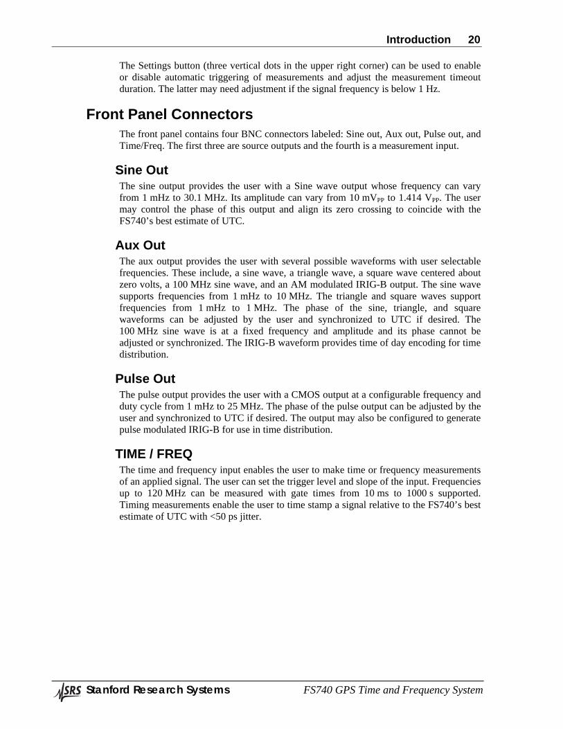
Front Panel Connectors The front panel contains four BNC connectors labeled: Sine out, Aux out, Pulse out, and Time/Freq. The first three are source outputs and the fourth is a measurement input.
Sine Out The sine output provides the user with a Sine wave output whose frequency can vary from 1 mHz to 30.1 MHz. Its amplitude can vary from 10 mVPP to 1.414 VPP. The user may control the phase of this output and align its zero crossing to coincide with the FS740’s best estimate of UTC.
Aux Out The aux output provides the user with several possible waveforms with user selectable frequencies. These include, a sine wave, a triangle wave, a square wave centered about zero volts, a 100 MHz sine wave, and an AM modulated IRIG-B output. The sine wave supports frequencies from 1 mHz to 10 MHz. The triangle and square waves support frequencies from 1 mHz to 1 MHz. The phase of the sine, triangle, and square waveforms can be adjusted by the user and synchronized to UTC if desired. The 100 MHz sine wave is at a fixed frequency and amplitude and its phase cannot be adjusted or synchronized. The IRIG-B waveform provides time of day encoding for time distribution.
Pulse Out The pulse output provides the user with a CMOS output at a configurable frequency and duty cycle from 1 mHz to 25 MHz. The phase of the pulse output can be adjusted by the user and synchronized to UTC if desired. The output may also be configured to generate pulse modulated IRIG-B for use in time distribution.
TIME / FREQ The time and frequency input enables the user to make time or frequency measurements of an applied signal. The user can set the trigger level and slope of the input. Frequencies up to 120 MHz can be measured with gate times from 10 ms to 1000 s supported. Timing measurements enable the user to time stamp a signal relative to the FS740’s best estimate of UTC with <50 ps jitter.
Introduction 21
Stanford Research Systems FS740 GPS Time and Frequency System
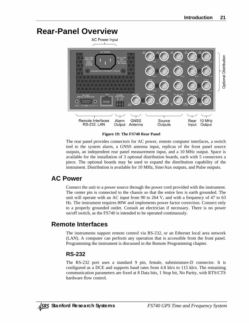
Rear-Panel Overview
Figure 19: The FS740 Rear Panel
The rear panel provides connectors for AC power, remote computer interfaces, a switch tied to the system alarm, a GNSS antenna input, replicas of the front panel source outputs, an independent rear panel measurement input, and a 10 MHz output. Space is available for the installation of 3 optional distribution boards, each with 5 connectors a piece. The optional boards may be used to expand the distribution capability of the instrument. Distribution is available for 10 MHz, Sine/Aux outputs, and Pulse outputs.
AC Power Connect the unit to a power source through the power cord provided with the instrument. The center pin is connected to the chassis so that the entire box is earth grounded. The unit will operate with an AC input from 90 to 264 V, and with a frequency of 47 to 63 Hz. The instrument requires 80W and implements power factor correction. Connect only to a properly grounded outlet. Consult an electrician if necessary. There is no power on/off switch, as the FS740 is intended to be operated continuously.
Remote Interfaces The instruments support remote control via RS-232, or an Ethernet local area network (LAN). A computer can perform any operation that is accessible from the front panel. Programming the instrument is discussed in the Remote Programming chapter.
RS-232 The RS-232 port uses a standard 9 pin, female, subminiature-D connector. It is configured as a DCE and supports baud rates from 4.8 kb/s to 115 kb/s. The remaining communication parameters are fixed at 8 Data bits, 1 Stop bit, No Parity, with RTS/CTS hardware flow control.
Introduction 22
Stanford Research Systems FS740 GPS Time and Frequency System
Ethernet The Ethernet uses a standard RJ-45 connector to connect to a local area network (LAN) using standard Category-5 or Category-6 cable. It supports both 10 and 100 Base-T Ethernet connections and a variety of TCP/IP configuration methods.
Alarm Relay This connector is tied to a 3A, SPDT switch, with normally open and normally closed connections. The alarm may be manually controlled, or configured to assert when in holdover or the timing error is large.
GNSS Antenna In order to lock to GNSS satellites, the FS740 must be connected to a GNSS antenna. The FS740 provides 5V power on the antenna input to support active antennas with more gain. The FS740 tries to detect fault conditions related to the antenna to alert the user of potential problems. If the current draw is too large, an antenna short fault is reported. Alternately, if the current draw is too small, an antenna open fault is reported.
Rear Measurement Input The FS740 provides a rear input for making time and frequency measurements that has completely independent measurement circuitry, which can function in parallel with the front panel input.
Source Outputs Sine Out
This is a duplicate of the front panel sine output. Its phase cannot be independently modified relative to the front panel output.
Aux Out This is a duplicate of the front panel aux output. Its phase cannot be independently modified relative to the front panel output.
Pulse Out This is a duplicate of the front panel pulse output. Its phase cannot be independently modified relative to the front panel output.
10 MHz Out The instrument also provides a 10 MHz output for referencing other instrumentation to the FS740’s internal reference. Its phase cannot be synchronized to UTC.
Option Boards The rear panel has space for the installation of up to 3 option boards for expanded distribution. Three different types of option boards are offered: Sine/Aux distribution, Pulse distribution, and 10 MHz distribution. The user may mix and match the installed options to meet application needs. Each board provides 5 buffered outputs of the desired signal. The Sine/Aux distribution options may be dynamically configured to provide 5 buffered duplicates of the Sine output, or 5 buffered duplicates of the Aux output. If
Introduction 23
Stanford Research Systems FS740 GPS Time and Frequency System
multiple Sine/Aux distribution option boards are installed, each one may be configured independently of the others. The other option boards have fixed configurations.

Basic Operation 25
Stanford Research Systems FS740 GPS Time and Frequency System
Operation
Introduction The previous chapter provided an overview of the instrument’s features and layout. This chapter describes the operation of the FS740 in detail and provides step by step instructions for setting up and configuring the FS740.
Global Navigation Systems Global navigation systems are satellite-based systems designed to provide a user with inexpensive, yet precise, position and timing information. There are four major constellations in operation today as detailed in Table 2. Collectively, these navigation systems are often referred to via the acronym GNSS.
Table 2: GNSS Navigation Systems
GNSS System Controlling Governments GPS United States GLONASS Russia BEIDOU China GALILEO European Union
GPS was the first navigation system deployed in 1995. It is the oldest and most mature navigation system in operation today. Russia soon followed with GLONASS. More recently, China’s BEIDOU and the European Union’s GALILEO navigation systems are coming online.
How Does GPS Work All four systems have similar performance and specifications. While the details between the various systems differ, the basic theory of operation is the same. For simplicity of presentation, we will highlight the various components that make up the GPS system. However, the basic concepts apply to other systems as well.
The Global Positioning System, or GPS, is a radio-navigation system which allows users with a clear view of the sky to identify their current position and time of day from any location around the globe. The system was originally designed for the military, but has been used for a wide variety of civil applications since its deployment, particularly in automobile and marine navigation. The system is managed and controlled by the United States Air Force (USAF). It consists of three parts: a space segment, a ground-based control segment, and the user segment.
The space segment consists of 24 satellites orbiting earth in 12 hour orbits at an altitude of approximately 20,200 km. The satellites are arranged into 6 equally spaced orbital planes with 4 satellites allocated to each plane. The organization is designed so that a user will always be able to view at least 4 satellites from virtually any location around the world. Atomic clocks on board the satellites maintain precise time of day
Basic Operation 26
Stanford Research Systems FS740 GPS Time and Frequency System
information. The satellites then broadcast ephemeris and time of day information to the user segment. A user with a view of at least 4 satellites can use this information to triangulate their position and time.
The control segment monitors the health of the satellites and uploads corrections and updates to the navigational information stored in the satellites. It is also in charge of decommissioning satellites when they have reached end of life, and the commissioning of new satellites to replace them. It consists of a master control station and a number of antennas and monitoring sites spread throughout the world.
The user segment consists of an antenna and a receiver which extracts the signals broadcast by the satellites. If the user can track at least 4 satellites, it has enough information to triangulate its position (latitude, longitude, height), and time of day.
Position can be resolved to a few meters. Time of day can be resolved to a few nanoseconds. For the FS740, it is this latter metric which is of significant importance. GPS time is monitored and maintained by a network of atomic clocks on the ground and aboard the satellites which are collectively steered to follow universal coordinated time (UTC) as maintained by the United States Naval Observatory (USNO). Thus, by locking its internal timebase to GPS, the FS740 can provide long term frequency stability on par with the best time keeping instrumentation in world, but at a fraction of the cost.
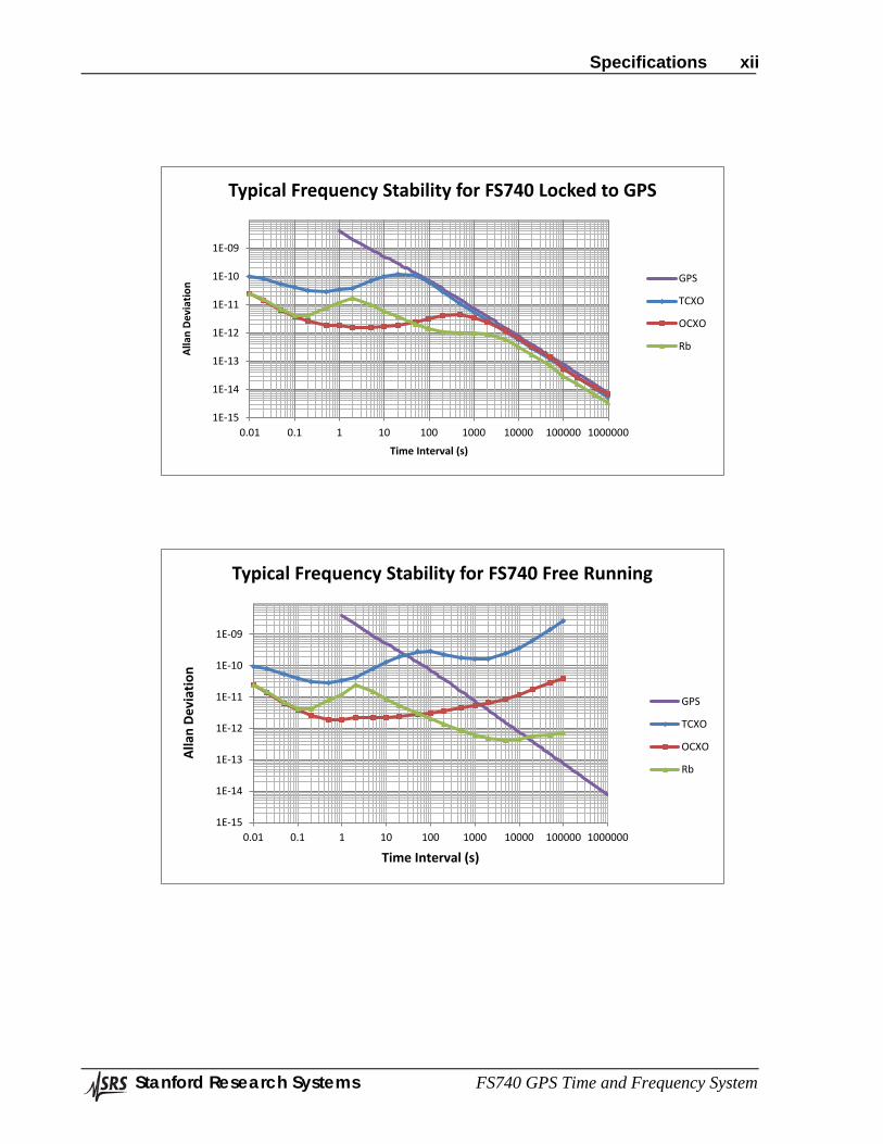
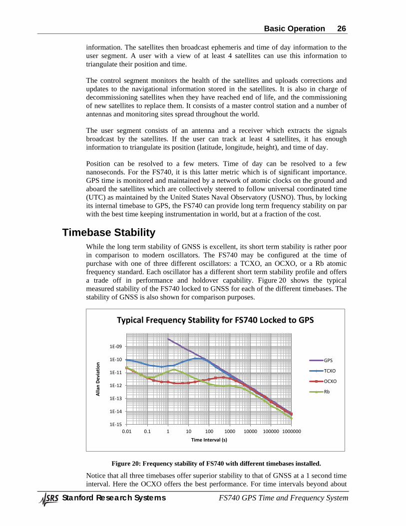
Timebase Stability While the long term stability of GNSS is excellent, its short term stability is rather poor in comparison to modern oscillators. The FS740 may be configured at the time of purchase with one of three different oscillators: a TCXO, an OCXO, or a Rb atomic frequency standard. Each oscillator has a different short term stability profile and offers a trade off in performance and holdover capability. Figure 20 shows the typical measured stability of the FS740 locked to GNSS for each of the different timebases. The stability of GNSS is also shown for comparison purposes.
Figure 20: Frequency stability of FS740 with different timebases installed.
Notice that all three timebases offer superior stability to that of GNSS at a 1 second time interval. Here the OCXO offers the best performance. For time intervals beyond about
1E-15
1E-14
1E-13
1E-12
1E-11
1E-10
1E-09
0.01 0.1 1 10 100 1000 10000 100000 1000000
Alla
n De
viat
ion
Time Interval (s)
Typical Frequency Stability for FS740 Locked to GPS
GPS
TCXO
OCXO
Rb
Basic Operation 27
Stanford Research Systems FS740 GPS Time and Frequency System
50 s the Rb oscillator outperforms. And for time intervals beyond about 5,000 s, all three timebases follow the performance of GNSS, with the Rb oscillator slightly outperforming the other timebases due to its ability to effectively average the GNSS signal over a longer time interval.
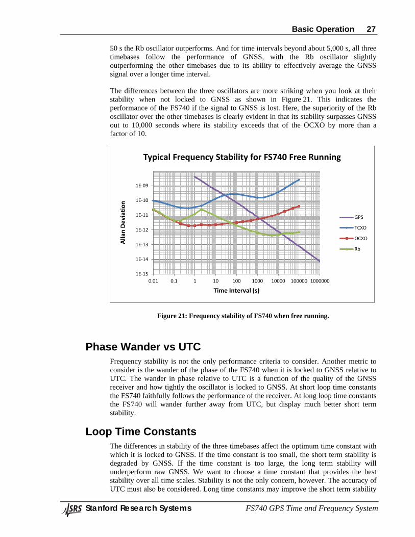
The differences between the three oscillators are more striking when you look at their stability when not locked to GNSS as shown in Figure 21. This indicates the performance of the FS740 if the signal to GNSS is lost. Here, the superiority of the Rb oscillator over the other timebases is clearly evident in that its stability surpasses GNSS out to 10,000 seconds where its stability exceeds that of the OCXO by more than a factor of 10.
Figure 21: Frequency stability of FS740 when free running.
Phase Wander vs UTC Frequency stability is not the only performance criteria to consider. Another metric to consider is the wander of the phase of the FS740 when it is locked to GNSS relative to UTC. The wander in phase relative to UTC is a function of the quality of the GNSS receiver and how tightly the oscillator is locked to GNSS. At short loop time constants the FS740 faithfully follows the performance of the receiver. At long loop time constants the FS740 will wander further away from UTC, but display much better short term stability.
Loop Time Constants The differences in stability of the three timebases affect the optimum time constant with which it is locked to GNSS. If the time constant is too small, the short term stability is degraded by GNSS. If the time constant is too large, the long term stability will underperform raw GNSS. We want to choose a time constant that provides the best stability over all time scales. Stability is not the only concern, however. The accuracy of UTC must also be considered. Long time constants may improve the short term stability
1E-15
1E-14
1E-13
1E-12
1E-11
1E-10
1E-09
0.01 0.1 1 10 100 1000 10000 100000 1000000
Alla
n De
viat
ion
Time Interval (s)
Typical Frequency Stability for FS740 Free Running
GPS
TCXO
OCXO
Rb
Basic Operation 28
Stanford Research Systems FS740 GPS Time and Frequency System
of Rb, for example, but they significantly degrade the accuracy of the FS740’s estimate of UTC. Thus, the selection of the loop time constant represents a tradeoff between several metrics of performance.
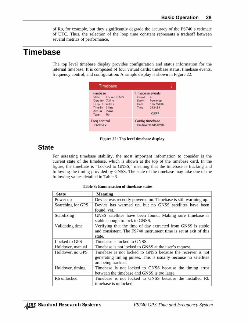
Timebase The top level timebase display provides configuration and status information for the internal timebase. It is composed of four virtual cards: timebase status, timebase events, frequency control, and configuration. A sample display is shown in Figure 22.
Figure 22: Top level timebase display
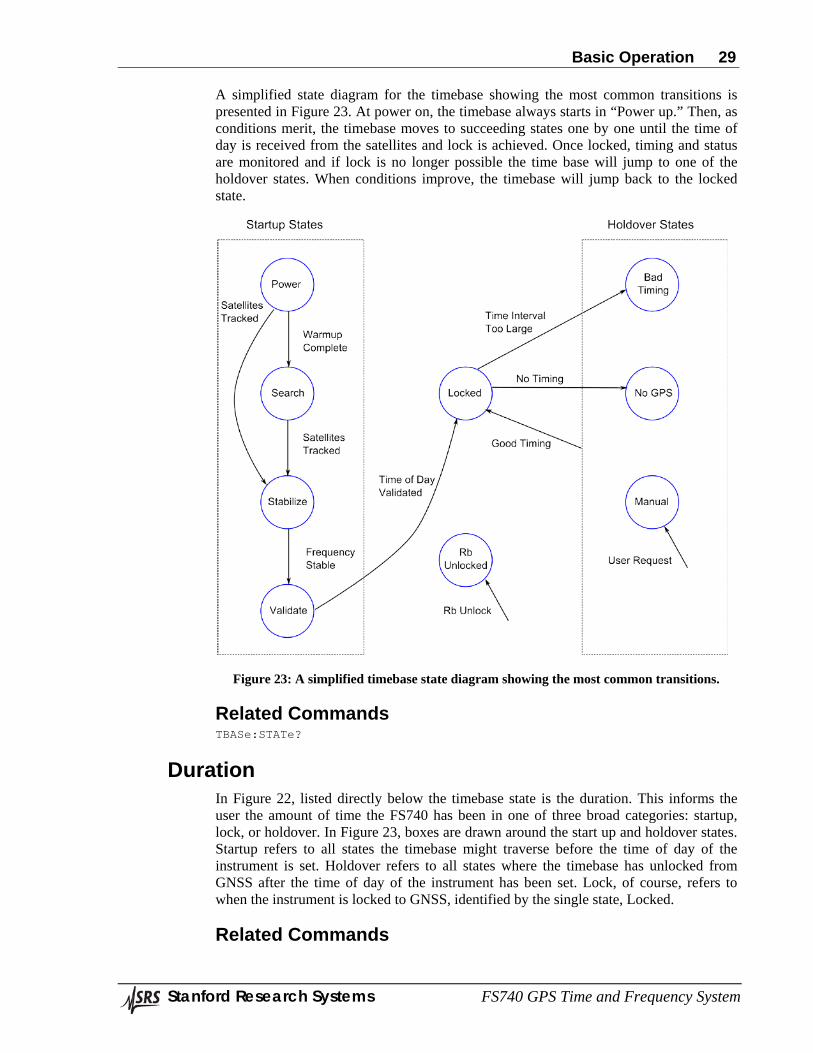
State For assessing timebase stability, the most important information to consider is the current state of the timebase, which is shown at the top of the timebase card. In the figure, the timebase is “Locked to GNSS,” meaning that the timebase is tracking and following the timing provided by GNSS. The state of the timebase may take one of the following values detailed in Table 3.
Table 3: Enumeration of timebase states
State Meaning Power up Device was recently powered on. Timebase is still warming up. Searching for GPS Device has warmed up, but no GNSS satellites have been
found, yet. Stabilizing GNSS satellites have been found. Making sure timebase is
stable enough to lock to GNSS. Validating time Verifying that the time of day extracted from GNSS is stable
and consistent. The FS740 instrument time is set at exit of this state.
Locked to GPS Timebase is locked to GNSS. Holdover, manual Timebase is not locked to GNSS at the user’s request. Holdover, no GPS Timebase is not locked to GNSS because the receiver is not
generating timing pulses. This is usually because no satellites are being tracked.
Holdover, timing Timebase is not locked to GNSS because the timing error between the timebase and GNSS is too large.
Rb unlocked Timebase is not locked to GNSS because the installed Rb timebase is unlocked.
Basic Operation 29
Stanford Research Systems FS740 GPS Time and Frequency System
A simplified state diagram for the timebase showing the most common transitions is presented in Figure 23. At power on, the timebase always starts in “Power up.” Then, as conditions merit, the timebase moves to succeeding states one by one until the time of day is received from the satellites and lock is achieved. Once locked, timing and status are monitored and if lock is no longer possible the time base will jump to one of the holdover states. When conditions improve, the timebase will jump back to the locked state.
Figure 23: A simplified timebase state diagram showing the most common transitions.
Related Commands TBASe:STATe?
Duration In Figure 22, listed directly below the timebase state is the duration. This informs the user the amount of time the FS740 has been in one of three broad categories: startup, lock, or holdover. In Figure 23, boxes are drawn around the start up and holdover states. Startup refers to all states the timebase might traverse before the time of day of the instrument is set. Holdover refers to all states where the timebase has unlocked from GNSS after the time of day of the instrument has been set. Lock, of course, refers to when the instrument is locked to GNSS, identified by the single state, Locked.
Related Commands
Basic Operation 30
Stanford Research Systems FS740 GPS Time and Frequency System
TBASe:STATe:HOLDover:DURation? TBASe:STATe:LOCK:DURation? TBASe:STATe:WARMup:DURation?
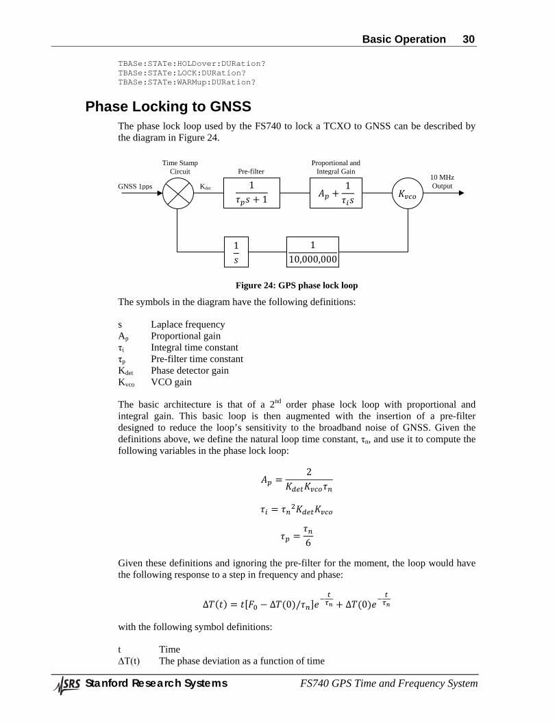
Phase Locking to GNSS The phase lock loop used by the FS740 to lock a TCXO to GNSS can be described by the diagram in Figure 24.
Figure 24: GPS phase lock loop
The symbols in the diagram have the following definitions:
s Laplace frequency Ap Proportional gain τi Integral time constant τp Pre-filter time constant Kdet Phase detector gain Kvco VCO gain
The basic architecture is that of a 2nd order phase lock loop with proportional and integral gain. This basic loop is then augmented with the insertion of a pre-filter designed to reduce the loop’s sensitivity to the broadband noise of GNSS. Given the definitions above, we define the natural loop time constant, τn, and use it to compute the following variables in the phase lock loop:
𝐴𝑝 =2
𝐾𝑑𝑒𝑡𝐾𝑣𝑣𝑣𝜏𝑛
𝜏𝑖 = 𝜏𝑛2𝐾𝑑𝑒𝑡𝐾𝑣𝑣𝑣
𝜏𝑝 =𝜏𝑛6
Given these definitions and ignoring the pre-filter for the moment, the loop would have the following response to a step in frequency and phase:
∆𝑇(𝑡) = 𝑡[𝐹0 − ∆𝑇(0)/𝜏𝑛]𝑒−𝑡𝜏𝑛 + ∆𝑇(0)𝑒−
𝑡𝜏𝑛
with the following symbol definitions:
t Time ∆T(t) The phase deviation as a function of time
1𝜏𝑝𝑠 + 1
𝐴𝑝 +1𝜏𝑖𝑠
𝐾𝑣𝑣𝑣
110,000,000
1𝑠
Pre-filter Proportional and
Integral Gain Time Stamp
Circuit
GNSS 1pps 10 MHz Output Kdet
Basic Operation 31
Stanford Research Systems FS740 GPS Time and Frequency System
∆T(0) The initial phase deviation at time t = 0 F0 The initial frequency offset at time t = 0 τn The natural loop time constant for the phase lock loop
The insertion of the pre-filter perturbs this solution slightly, but the overall response is very similar. The speed with which the FS740 follows GNSS is controlled by the natural loop time constant, τn. By shortening, the time constant, the FS740 will follow GNSS more faithfully, including the broadband noise of GNSS. By extending the time constant to longer time scales, the FS740 will continue to follow GNSS over the long term, but rely on its own stability for short term performance. The goal is to select a time constant that reflects the best balance between short and long term performance for the loop.
Predictive Filtering The superior short term stabilities of the OCXO and Rb timebases enable the usage of predictive filtering to improve the stability of the FS740 by up to 3 times over traditional methods. Predictive filtering uses state space methods to predict the phase of the local timebase relative to GNSS. The technique is quite similar to Kalman filtering. The benefit is that the FS740 can average the GNSS signal much more effectively, resulting in a significantly more stable signal with a much shorter time constant than would be possible with traditional filtering.
Optimum Time Constant The FS740 may be configured at the time of purchase with one of three different timebases: a TCXO, an OCXO, and a Rb atomic frequency standard. The optimum time constant for locking each of these timebases to GNSS is different, and detailed in Table 4.
Table 4: Optimum loop time constants
Timebase Optimum loop time constant TCXO 8 s OCXO 250 s Rb 2000 s
Although these are the optimum time constants when everything has stabilized, they are not ideal during warm-up or when the FS740 first locks to GNSS. During these times it is preferable to have a short time constant so that the FS740 may quickly align its phase and frequency with GNSS. Therefore, the FS740 will automatically reduce the time constant to as little as 3 s so that it may quickly align its phase to that of GNSS. Once adequate phase alignment has been achieved, the time constant will be gradually increased to the optimum time constant detailed in Table 4. Optimum frequency stability is not achieved, however, until the time constant reaches the optimum time constant.
Current Time Constant and Timing Error In Figure 22 on page 28, listed directly below duration, is the current loop time constant for the phase lock loop, the most recent timing error, and the average timing error of the timebase relative to GNSS. Positive errors indicate the timebase lags GNSS. Negative errors indicate the timebase leads GNSS. The most recent error represents the output of the time stamp circuit in Figure 24. The average error represents the output of the pre-filter.
Basic Operation 32
Stanford Research Systems FS740 GPS Time and Frequency System
Related Commands TBASe:TCONstant TBASe:TINTerval
Installed Timebase In Figure 22, listed at the bottom of the Timebase card is the installed timebase. In the figure the timebase is a Rb atomic frequency standard.
Related Commands *OPT?
Timebase Events The FS740 automatically captures each time the state of the timebase changes as an event. Every time the timebase either locks or unlocks from GNSS, for instance, the event will be logged. These events may be viewed one by one on the Timebase events card. The FS740 has room to store up to 10 events. If more than 10 events occur, the oldest event is discarded to make room.
The event queue provides the user with automatic self monitoring capability. The user need not continually query the state of the timebase. Rather, he or she can view the event log to see if anything happened over the time period of interest. By comparing time stamps, one can easily deduce how long the timebase spent in each state.
Related Commands TBASe:EVENt:CLEar TBASe:EVENt:COUNt TBASe:EVENt:NEXT?
Frequency Control The frequency control voltage is the voltage applied to the electronic frequency control input of the timebase to maintain lock to GNSS. It is updated every second by the digital phase lock loop when the receiver is generating timing pulses. Every 24 hours of phase lock to GPS the FS740 will automatically save the current frequency control value so that the timebase will power up at a value close to optimum if GNSS is not present.
When the timebase is locked to GNSS, the frequency control value cannot be changed by the user. If the timebase is not locked to GNSS, however, the user may change the frequency of the timebase by updating this voltage. The user may force the FS740 to unlock from GNSS, if necessary, to make this possible. See section Lock to GNSS on page 33 for details.
Related Commands TBASe:FCONtrol TBASe:FCONtrol:SAVe
Configuration By default, the FS740 will initially lock to GNSS with a short time constant and then gradually extend the time constant to the optimum value for the given timebase when phase alignment is achieved. The user may modify this default configuration by pressing
Basic Operation 33
Stanford Research Systems FS740 GPS Time and Frequency System
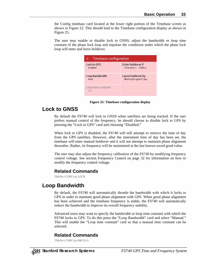
the Config timebase card located at the lower right portion of the Timebase screen as shown in Figure 22. This should lead to the Timebase configuration display as shown in Figure 25.
The user may enable or disable lock to GNSS, adjust the bandwidth or loop time constant of the phase lock loop and stipulate the conditions under which the phase lock loop will enter and leave holdover.
Figure 25: Timebase configuration display
Lock to GNSS By default the FS740 will lock to GNSS when satellites are being tracked. If the user prefers manual control of the frequency, he should choose to disable lock to GPS by pressing the “Lock to GPS” card and choosing “Disabled.”
When lock to GPS is disabled, the FS740 will still attempt to retrieve the time of day from the GPS satellites. However, after the instrument time of day has been set, the timebase will enter manual holdover and it will not attempt to maintain phase alignment thereafter. Rather, its frequency will be maintained at the last known saved good value.
The user may also adjust the frequency calibration of the FS740 by modifying frequency control voltage. See section Frequency Control on page 32 for information on how to modify the frequency control voltage.
Related Commands TBASe:CONFig:LOCK
Loop Bandwidth By default, the FS740 will automatically throttle the bandwidth with which it locks to GPS in order to maintain good phase alignment with GPS. When good phase alignment has been achieved and the timebase frequency is stable, the FS740 will automatically reduce the bandwidth to improve its overall frequency stability.
Advanced users may want to specify the bandwidth or loop time constant with which the FS740 locks to GPS. To do this press the “Loop Bandwidth” card and select “Manual.” This will enable the “Loop time constant” card so that a manual time constant can be selected.
Related Commands TBASe:CONFig:BWIDth
Basic Operation 34
Stanford Research Systems FS740 GPS Time and Frequency System
Loop Time Constant The “Loop time constant” card is only enabled when manual loop bandwidth control is selected. See section Loop Bandwidth above for details. This setting enables the user to specify the phase lock loop time constant with which the FS740 locks to GPS. To change the time constant, press the “Loop time constant” card and enter a new time constant in seconds. See section Phase Locking to GNSS on page 30 for details on the phase lock loop used by the FS740 to lock to GPS and the optimum time constants for each timebase. Short time constants force the FS740 to faithfully follow the phase of GPS including its noise. Longer time constants improve the short term stability of the FS740 but also may increase the wander of its estimate of UTC.
Related Commands TBASe:TCONstant
Criteria to Enter Holdover When locked to GPS the FS740 will try to adjust its frequency to maintain good phase alignment with GPS. Under normal conditions this is preferred. Under abnormal conditions, however, this may no longer be desirable, particularly if the measured timing error is large.
There are two scenarios worth considering. In the more common scenario the FS740 may lose the GPS signal for an extended period of time, during which the phase of the FS740 will drift away from alignment. At some point the FS740 may reacquire the GPS signal and see that its phase has drifted significantly away from alignment. How should the FS740 recover? Should it slew the phase back by adjusting its frequency, or should it jump phase instantaneously to the new location?
The second scenario to consider is when the GPS receiver generates rogue timing pulses due to processing incorrect timing information from a failing satellite, having timing data corrupted by noise, or possibly a firmware bug within the GPS receiver itself. In this scenario the GPS timing pulses may suddenly jump in phase. Again the user must decide how the FS740 should recover.
The decision can be broken down into two parts. The first, to be decided here, is the maximum measured timing error allowed before the FS740 will abandon lock and enter holdover. The default is 1 μs. To modify this limit, press the card “Enter holdover if” and enter a new limit.
The second part, to be decided in the next section, is how to recover from holdover.
Related Commands TBASe:CONFig:TINTerval:LIMit
Criteria to Leave Holdover The FS740 may enter holdover for a number of reasons, the most common of which is that it lost the GPS signal for a time. When it regains the GPS signal, how should it respond? If the timing error is less than the threshold set above, then the FS740 will proceed as if it never lost lock. If the timing error is greater than the threshold set above, then the FS740 has three options:
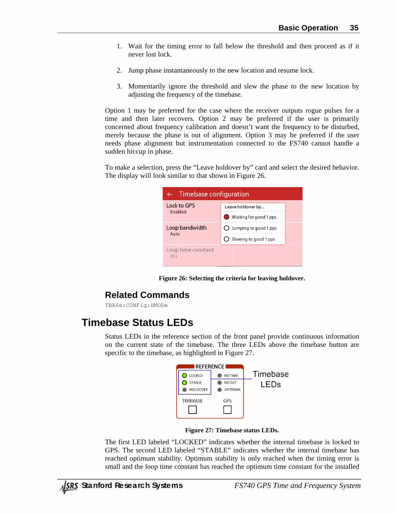
Basic Operation 35
Stanford Research Systems FS740 GPS Time and Frequency System
1. Wait for the timing error to fall below the threshold and then proceed as if it never lost lock.
2. Jump phase instantaneously to the new location and resume lock.
3. Momentarily ignore the threshold and slew the phase to the new location by adjusting the frequency of the timebase.
Option 1 may be preferred for the case where the receiver outputs rogue pulses for a time and then later recovers. Option 2 may be preferred if the user is primarily concerned about frequency calibration and doesn’t want the frequency to be disturbed, merely because the phase is out of alignment. Option 3 may be preferred if the user needs phase alignment but instrumentation connected to the FS740 cannot handle a sudden hiccup in phase.
To make a selection, press the “Leave holdover by” card and select the desired behavior. The display will look similar to that shown in Figure 26.
Figure 26: Selecting the criteria for leaving holdover.
Related Commands TBASe:CONFig:HMODe
Timebase Status LEDs Status LEDs in the reference section of the front panel provide continuous information on the current state of the timebase. The three LEDs above the timebase button are specific to the timebase, as highlighted in Figure 27.
Figure 27: Timebase status LEDs.
The first LED labeled “LOCKED” indicates whether the internal timebase is locked to GPS. The second LED labeled “STABLE” indicates whether the internal timebase has reached optimum stability. Optimum stability is only reached when the timing error is small and the loop time constant has reached the optimum time constant for the installed
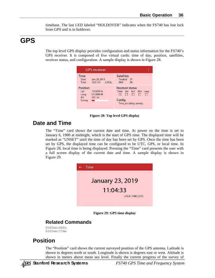
Basic Operation 36
Stanford Research Systems FS740 GPS Time and Frequency System
timebase. The last LED labeled “HOLDOVER” indicates when the FS740 has lost lock from GPS and is in holdover.
GPS The top level GPS display provides configuration and status information for the FS740’s GPS receiver. It is composed of five virtual cards: time of day, position, satellites, receiver status, and configuration. A sample display is shown in Figure 28.
Figure 28: Top level GPS display
Date and Time The “Time” card shows the current date and time. At power on the time is set to January 6, 1980 at midnight, which is the start of GPS time. The displayed time will be marked as “UNSET” until the time of day has been set by GPS. Once the time has been set by GPS, the displayed time can be configured to be UTC, GPS, or local time. In Figure 28, local time is being displayed. Pressing the “Time” card presents the user with a full screen display of the current date and time. A sample display is shown in Figure 29.
Figure 29: GPS time display
Related Commands SYSTem:DATe SYSTem:TIMe
Position The “Position” card shows the current surveyed position of the GPS antenna. Latitude is shown in degrees north or south. Longitude is shown is degrees east or west. Altitude is shown in meters above mean sea level. Finally the current progress of the survey of
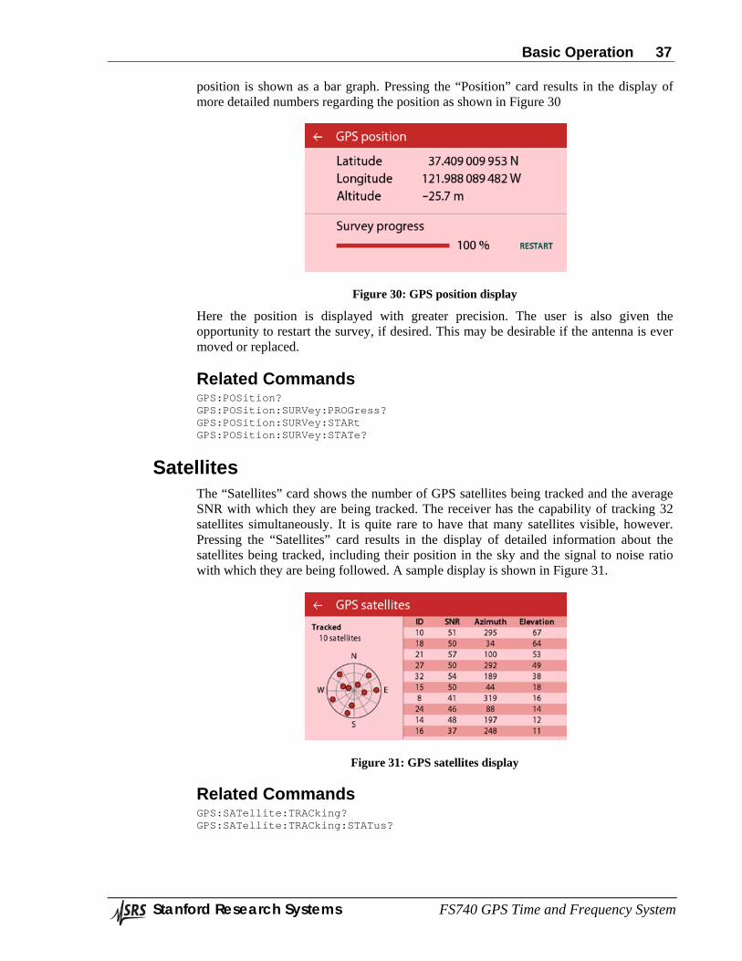
Basic Operation 37
Stanford Research Systems FS740 GPS Time and Frequency System
position is shown as a bar graph. Pressing the “Position” card results in the display of more detailed numbers regarding the position as shown in Figure 30
Figure 30: GPS position display
Here the position is displayed with greater precision. The user is also given the opportunity to restart the survey, if desired. This may be desirable if the antenna is ever moved or replaced.
Related Commands GPS:POSition? GPS:POSition:SURVey:PROGress? GPS:POSition:SURVey:STARt GPS:POSition:SURVey:STATe?
Satellites The “Satellites” card shows the number of GPS satellites being tracked and the average SNR with which they are being tracked. The receiver has the capability of tracking 32 satellites simultaneously. It is quite rare to have that many satellites visible, however. Pressing the “Satellites” card results in the display of detailed information about the satellites being tracked, including their position in the sky and the signal to noise ratio with which they are being followed. A sample display is shown in Figure 31.
Figure 31: GPS satellites display
Related Commands GPS:SATellite:TRACking? GPS:SATellite:TRACking:STATus?
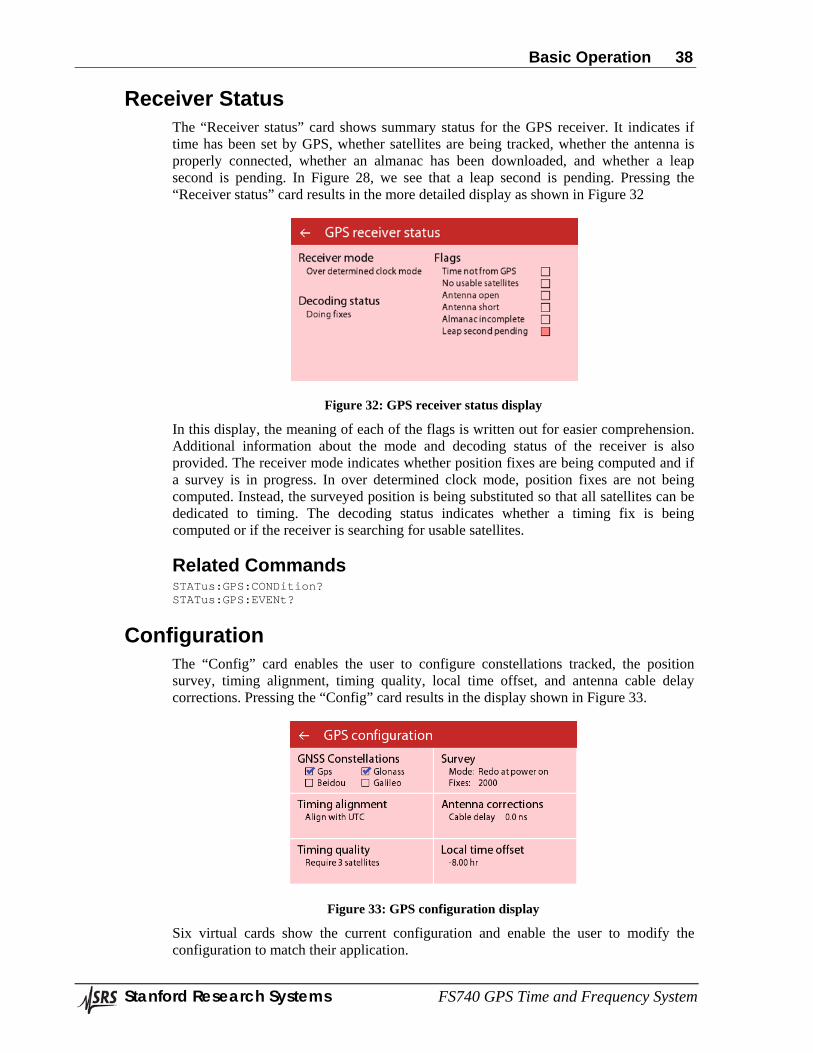
Basic Operation 38
Stanford Research Systems FS740 GPS Time and Frequency System
Receiver Status The “Receiver status” card shows summary status for the GPS receiver. It indicates if time has been set by GPS, whether satellites are being tracked, whether the antenna is properly connected, whether an almanac has been downloaded, and whether a leap second is pending. In Figure 28, we see that a leap second is pending. Pressing the “Receiver status” card results in the more detailed display as shown in Figure 32
Figure 32: GPS receiver status display
In this display, the meaning of each of the flags is written out for easier comprehension. Additional information about the mode and decoding status of the receiver is also provided. The receiver mode indicates whether position fixes are being computed and if a survey is in progress. In over determined clock mode, position fixes are not being computed. Instead, the surveyed position is being substituted so that all satellites can be dedicated to timing. The decoding status indicates whether a timing fix is being computed or if the receiver is searching for usable satellites.
Related Commands STATus:GPS:CONDition? STATus:GPS:EVENt?
Configuration The “Config” card enables the user to configure constellations tracked, the position survey, timing alignment, timing quality, local time offset, and antenna cable delay corrections. Pressing the “Config” card results in the display shown in Figure 33.
Figure 33: GPS configuration display
Six virtual cards show the current configuration and enable the user to modify the configuration to match their application.
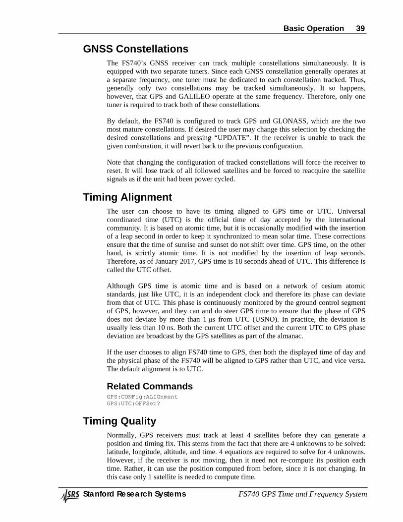
Basic Operation 39
Stanford Research Systems FS740 GPS Time and Frequency System
GNSS Constellations The FS740’s GNSS receiver can track multiple constellations simultaneously. It is equipped with two separate tuners. Since each GNSS constellation generally operates at a separate frequency, one tuner must be dedicated to each constellation tracked. Thus, generally only two constellations may be tracked simultaneously. It so happens, however, that GPS and GALILEO operate at the same frequency. Therefore, only one tuner is required to track both of these constellations.
By default, the FS740 is configured to track GPS and GLONASS, which are the two most mature constellations. If desired the user may change this selection by checking the desired constellations and pressing “UPDATE”. If the receiver is unable to track the given combination, it will revert back to the previous configuration.
Note that changing the configuration of tracked constellations will force the receiver to reset. It will lose track of all followed satellites and be forced to reacquire the satellite signals as if the unit had been power cycled.
Timing Alignment The user can choose to have its timing aligned to GPS time or UTC. Universal coordinated time (UTC) is the official time of day accepted by the international community. It is based on atomic time, but it is occasionally modified with the insertion of a leap second in order to keep it synchronized to mean solar time. These corrections ensure that the time of sunrise and sunset do not shift over time. GPS time, on the other hand, is strictly atomic time. It is not modified by the insertion of leap seconds. Therefore, as of January 2017, GPS time is 18 seconds ahead of UTC. This difference is called the UTC offset.
Although GPS time is atomic time and is based on a network of cesium atomic standards, just like UTC, it is an independent clock and therefore its phase can deviate from that of UTC. This phase is continuously monitored by the ground control segment of GPS, however, and they can and do steer GPS time to ensure that the phase of GPS does not deviate by more than 1 μs from UTC (USNO). In practice, the deviation is usually less than 10 ns. Both the current UTC offset and the current UTC to GPS phase deviation are broadcast by the GPS satellites as part of the almanac.
If the user chooses to align FS740 time to GPS, then both the displayed time of day and the physical phase of the FS740 will be aligned to GPS rather than UTC, and vice versa. The default alignment is to UTC.
Related Commands GPS:CONFig:ALIGnment GPS:UTC:OFFSet?
Timing Quality Normally, GPS receivers must track at least 4 satellites before they can generate a position and timing fix. This stems from the fact that there are 4 unknowns to be solved: latitude, longitude, altitude, and time. 4 equations are required to solve for 4 unknowns. However, if the receiver is not moving, then it need not re-compute its position each time. Rather, it can use the position computed from before, since it is not changing. In this case only 1 satellite is needed to compute time.
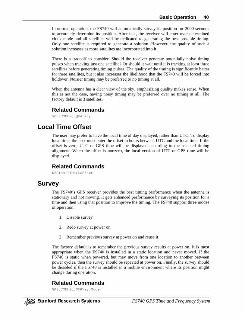
Basic Operation 40
Stanford Research Systems FS740 GPS Time and Frequency System
In normal operation, the FS740 will automatically survey its position for 2000 seconds to accurately determine its position. After that, the receiver will enter over determined clock mode and all satellites will be dedicated to generating the best possible timing. Only one satellite is required to generate a solution. However, the quality of such a solution increases as more satellites are incorporated into it.
There is a tradeoff to consider. Should the receiver generate potentially noisy timing pulses when tracking just one satellite? Or should it wait until it is tracking at least three satellites before generating timing pulses. The quality of the timing is significantly better for three satellites, but it also increases the likelihood that the FS740 will be forced into holdover. Noisier timing may be preferred to no timing at all.
When the antenna has a clear view of the sky, emphasizing quality makes sense. When this is not the case, having noisy timing may be preferred over no timing at all. The factory default is 3 satellites.
Related Commands GPS:CONFig:QUALity
Local Time Offset The user may prefer to have the local time of day displayed, rather than UTC. To display local time, the user must enter the offset in hours between UTC and the local time. If the offset is zero, UTC or GPS time will be displayed according to the selected timing alignment. When the offset is nonzero, the local version of UTC or GPS time will be displayed.
Related Commands SYSTem:TIMe:LOFFset
Survey The FS740’s GPS receiver provides the best timing performance when the antenna is stationary and not moving. It gets enhanced performance by surveying its position for a time and then using that position to improve the timing. The FS740 support three modes of operation:
1. Disable survey
2. Redo survey at power on
3. Remember previous survey at power on and reuse it
The factory default is to remember the previous survey results at power on. It is most appropriate when the FS740 is installed in a static location and never moved. If the FS740 is static when powered, but may move from one location to another between power cycles, then the survey should be repeated at power on. Finally, the survey should be disabled if the FS740 is installed in a mobile environment where its position might change during operation.
Related Commands GPS:CONFig:SURVey:Mode
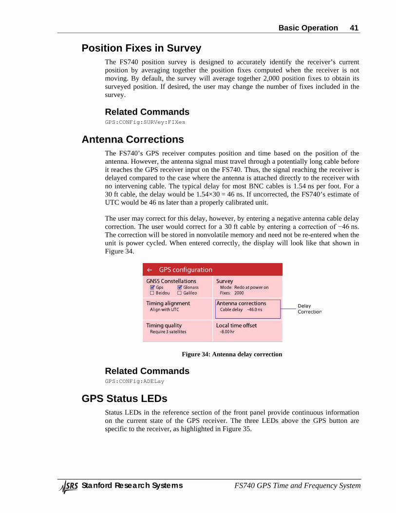
Basic Operation 41
Stanford Research Systems FS740 GPS Time and Frequency System
Position Fixes in Survey The FS740 position survey is designed to accurately identify the receiver’s current position by averaging together the position fixes computed when the receiver is not moving. By default, the survey will average together 2,000 position fixes to obtain its surveyed position. If desired, the user may change the number of fixes included in the survey.
Related Commands GPS:CONFig:SURVey:FIXes
Antenna Corrections The FS740’s GPS receiver computes position and time based on the position of the antenna. However, the antenna signal must travel through a potentially long cable before it reaches the GPS receiver input on the FS740. Thus, the signal reaching the receiver is delayed compared to the case where the antenna is attached directly to the receiver with no intervening cable. The typical delay for most BNC cables is 1.54 ns per foot. For a 30 ft cable, the delay would be 1.54×30 = 46 ns. If uncorrected, the FS740’s estimate of UTC would be 46 ns later than a properly calibrated unit.
The user may correct for this delay, however, by entering a negative antenna cable delay correction. The user would correct for a 30 ft cable by entering a correction of −46 ns. The correction will be stored in nonvolatile memory and need not be re-entered when the unit is power cycled. When entered correctly, the display will look like that shown in Figure 34.
Figure 34: Antenna delay correction
Related Commands GPS:CONFig:ADELay
GPS Status LEDs Status LEDs in the reference section of the front panel provide continuous information on the current state of the GPS receiver. The three LEDs above the GPS button are specific to the receiver, as highlighted in Figure 35.
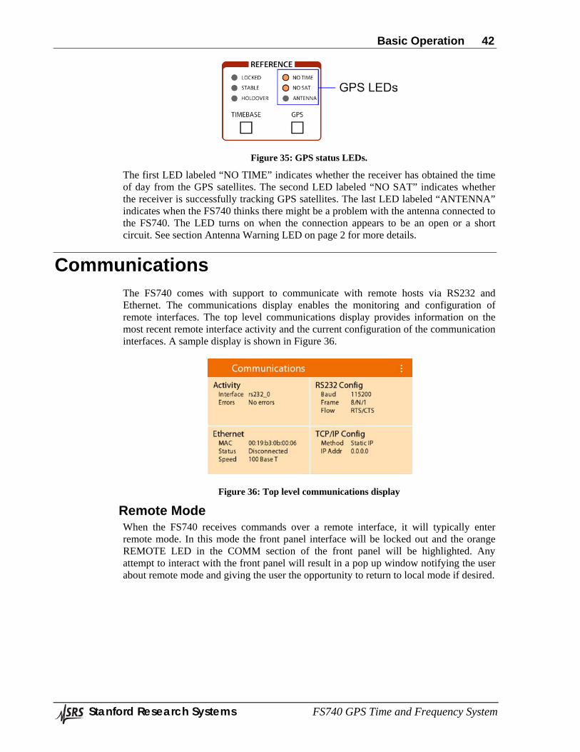
Basic Operation 42
Stanford Research Systems FS740 GPS Time and Frequency System
Figure 35: GPS status LEDs.
The first LED labeled “NO TIME” indicates whether the receiver has obtained the time of day from the GPS satellites. The second LED labeled “NO SAT” indicates whether the receiver is successfully tracking GPS satellites. The last LED labeled “ANTENNA” indicates when the FS740 thinks there might be a problem with the antenna connected to the FS740. The LED turns on when the connection appears to be an open or a short circuit. See section Antenna Warning LED on page 2 for more details.
Communications The FS740 comes with support to communicate with remote hosts via RS232 and Ethernet. The communications display enables the monitoring and configuration of remote interfaces. The top level communications display provides information on the most recent remote interface activity and the current configuration of the communication interfaces. A sample display is shown in Figure 36.
Figure 36: Top level communications display
Remote Mode When the FS740 receives commands over a remote interface, it will typically enter remote mode. In this mode the front panel interface will be locked out and the orange REMOTE LED in the COMM section of the front panel will be highlighted. Any attempt to interact with the front panel will result in a pop up window notifying the user about remote mode and giving the user the opportunity to return to local mode if desired.
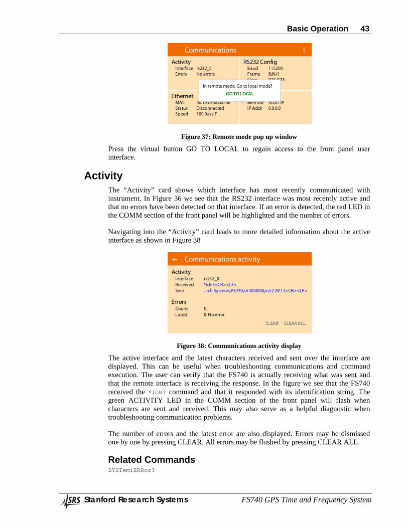
Basic Operation 43
Stanford Research Systems FS740 GPS Time and Frequency System
Figure 37: Remote mode pop up window
Press the virtual button GO TO LOCAL to regain access to the front panel user interface.
Activity The “Activity” card shows which interface has most recently communicated with instrument. In Figure 36 we see that the RS232 interface was most recently active and that no errors have been detected on that interface. If an error is detected, the red LED in the COMM section of the front panel will be highlighted and the number of errors.
Navigating into the “Activity” card leads to more detailed information about the active interface as shown in Figure 38
Figure 38: Communications activity display
The active interface and the latest characters received and sent over the interface are displayed. This can be useful when troubleshooting communications and command execution. The user can verify that the FS740 is actually receiving what was sent and that the remote interface is receiving the response. In the figure we see that the FS740 received the *IDN? command and that it responded with its identification string. The green ACTIVITY LED in the COMM section of the front panel will flash when characters are sent and received. This may also serve as a helpful diagnostic when troubleshooting communication problems.
The number of errors and the latest error are also displayed. Errors may be dismissed one by one by pressing CLEAR. All errors may be flushed by pressing CLEAR ALL.
Related Commands SYSTem:ERRor?
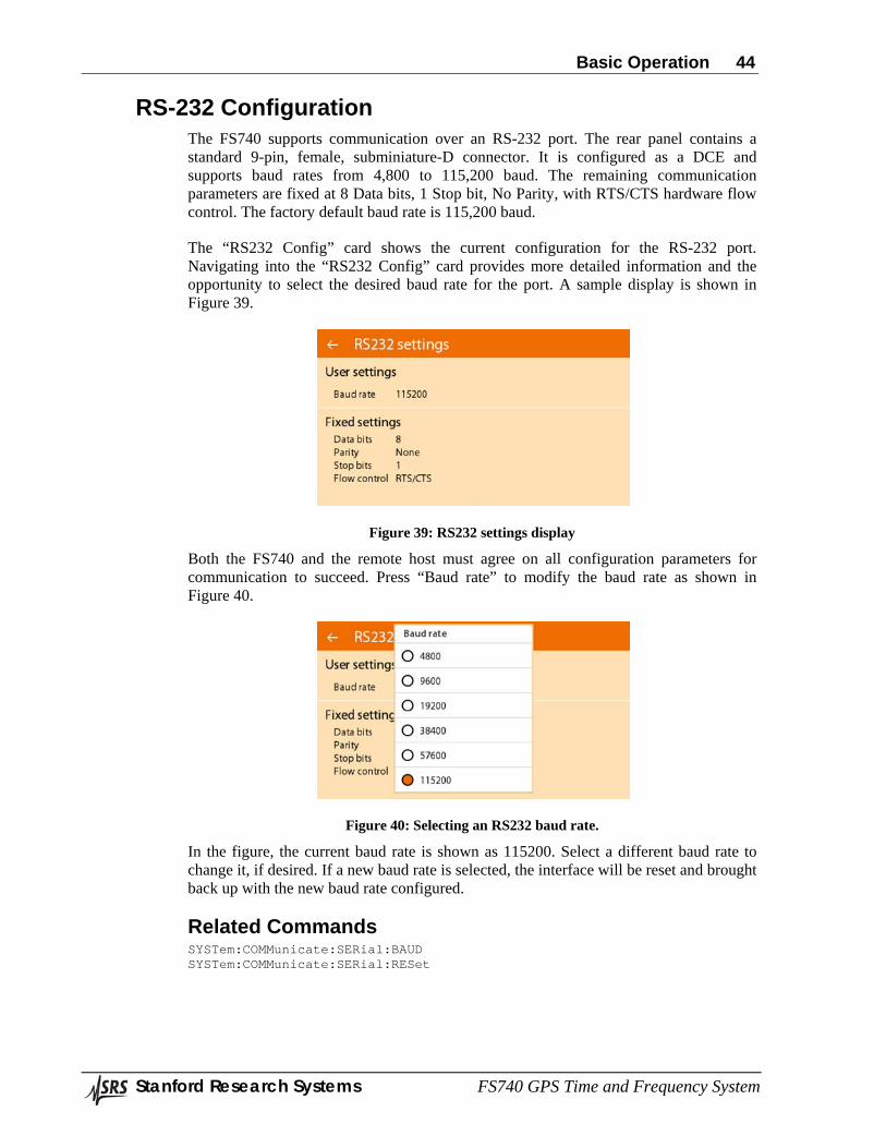
Basic Operation 44
Stanford Research Systems FS740 GPS Time and Frequency System
RS-232 Configuration The FS740 supports communication over an RS-232 port. The rear panel contains a standard 9-pin, female, subminiature-D connector. It is configured as a DCE and supports baud rates from 4,800 to 115,200 baud. The remaining communication parameters are fixed at 8 Data bits, 1 Stop bit, No Parity, with RTS/CTS hardware flow control. The factory default baud rate is 115,200 baud.
The “RS232 Config” card shows the current configuration for the RS-232 port. Navigating into the “RS232 Config” card provides more detailed information and the opportunity to select the desired baud rate for the port. A sample display is shown in Figure 39.
Figure 39: RS232 settings display
Both the FS740 and the remote host must agree on all configuration parameters for communication to succeed. Press “Baud rate” to modify the baud rate as shown in Figure 40.
Figure 40: Selecting an RS232 baud rate.
In the figure, the current baud rate is shown as 115200. Select a different baud rate to change it, if desired. If a new baud rate is selected, the interface will be reset and brought back up with the new baud rate configured.
Related Commands SYSTem:COMMunicate:SERial:BAUD SYSTem:COMMunicate:SERial:RESet
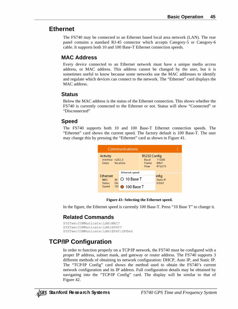
Basic Operation 45
Stanford Research Systems FS740 GPS Time and Frequency System
Ethernet The FS740 may be connected to an Ethernet based local area network (LAN). The rear panel contains a standard RJ-45 connector which accepts Category-5 or Category-6 cable. It supports both 10 and 100 Base-T Ethernet connection speeds.
MAC Address Every device connected to an Ethernet network must have a unique media access address, or MAC address. This address cannot be changed by the user, but it is sometimes useful to know because some networks use the MAC addresses to identify and regulate which devices can connect to the network. The “Ethernet” card displays the MAC address.
Status Below the MAC address is the status of the Ethernet connection. This shows whether the FS740 is currently connected to the Ethernet or not. Status will show “Connected” or “Disconnected”
Speed The FS740 supports both 10 and 100 Base-T Ethernet connection speeds. The “Ethernet” card shows the current speed. The factory default is 100 Base-T. The user may change this by pressing the “Ethernet” card as shown in Figure 41.
Figure 41: Selecting the Ethernet speed.
In the figure, the Ethernet speed is currently 100 Base-T. Press “10 Base T” to change it.
Related Commands SYSTem:COMMunicate:LAN:MAC? SYSTem:COMMunicate:LAN:EPHY? SYSTem:COMMunicate:LAN:EPHY:SPEed
TCP/IP Configuration In order to function properly on a TCP/IP network, the FS740 must be configured with a proper IP address, subnet mask, and gateway or router address. The FS740 supports 3 different methods of obtaining its network configuration: DHCP, Auto IP, and Static IP. The “TCP/IP Config” card shows the method used to obtain the FS740’s current network configuration and its IP address. Full configuration details may be obtained by navigating into the “TCP/IP Config” card. The display will be similar to that of Figure 42.
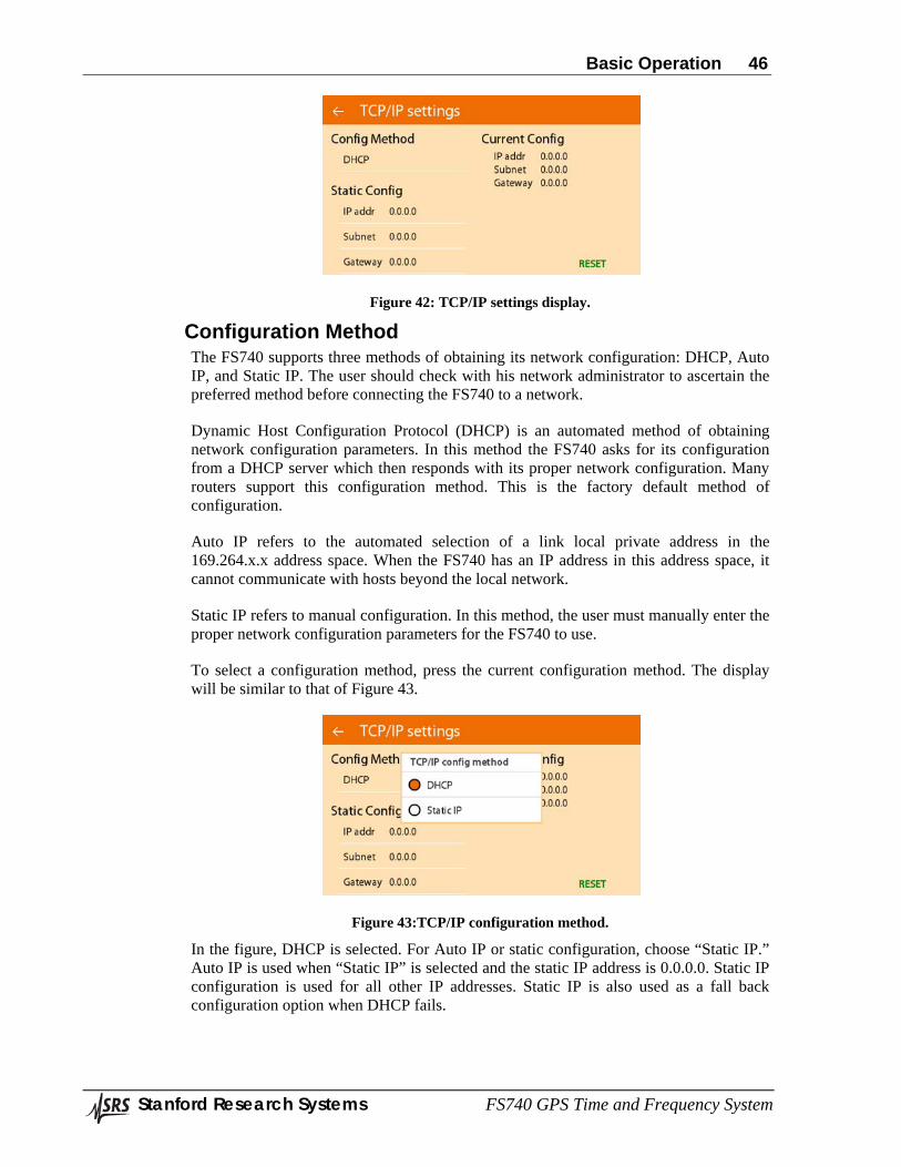
Basic Operation 46
Stanford Research Systems FS740 GPS Time and Frequency System
Figure 42: TCP/IP settings display.
Configuration Method The FS740 supports three methods of obtaining its network configuration: DHCP, Auto IP, and Static IP. The user should check with his network administrator to ascertain the preferred method before connecting the FS740 to a network.
Dynamic Host Configuration Protocol (DHCP) is an automated method of obtaining network configuration parameters. In this method the FS740 asks for its configuration from a DHCP server which then responds with its proper network configuration. Many routers support this configuration method. This is the factory default method of configuration.
Auto IP refers to the automated selection of a link local private address in the 169.264.x.x address space. When the FS740 has an IP address in this address space, it cannot communicate with hosts beyond the local network.
Static IP refers to manual configuration. In this method, the user must manually enter the proper network configuration parameters for the FS740 to use.
To select a configuration method, press the current configuration method. The display will be similar to that of Figure 43.
Figure 43:TCP/IP configuration method.
In the figure, DHCP is selected. For Auto IP or static configuration, choose “Static IP.” Auto IP is used when “Static IP” is selected and the static IP address is 0.0.0.0. Static IP configuration is used for all other IP addresses. Static IP is also used as a fall back configuration option when DHCP fails.
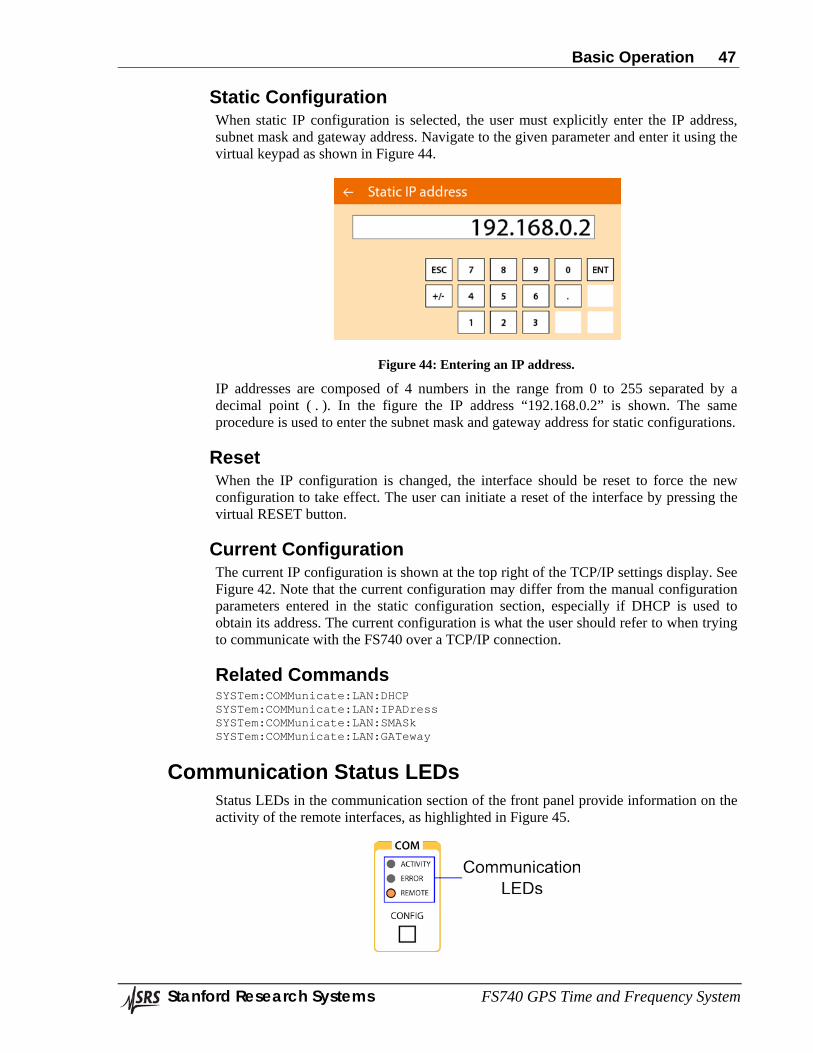
Basic Operation 47
Stanford Research Systems FS740 GPS Time and Frequency System
Static Configuration When static IP configuration is selected, the user must explicitly enter the IP address, subnet mask and gateway address. Navigate to the given parameter and enter it using the virtual keypad as shown in Figure 44.
Figure 44: Entering an IP address.
IP addresses are composed of 4 numbers in the range from 0 to 255 separated by a decimal point ( . ). In the figure the IP address “192.168.0.2” is shown. The same procedure is used to enter the subnet mask and gateway address for static configurations.
Reset When the IP configuration is changed, the interface should be reset to force the new configuration to take effect. The user can initiate a reset of the interface by pressing the virtual RESET button.
Current Configuration The current IP configuration is shown at the top right of the TCP/IP settings display. See Figure 42. Note that the current configuration may differ from the manual configuration parameters entered in the static configuration section, especially if DHCP is used to obtain its address. The current configuration is what the user should refer to when trying to communicate with the FS740 over a TCP/IP connection.
Related Commands SYSTem:COMMunicate:LAN:DHCP SYSTem:COMMunicate:LAN:IPADress SYSTem:COMMunicate:LAN:SMASk SYSTem:COMMunicate:LAN:GATeway
Communication Status LEDs Status LEDs in the communication section of the front panel provide information on the activity of the remote interfaces, as highlighted in Figure 45.
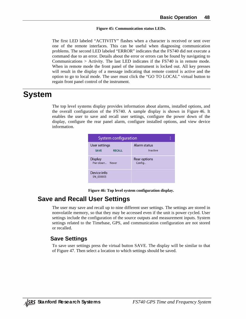
Basic Operation 48
Stanford Research Systems FS740 GPS Time and Frequency System
Figure 45: Communication status LEDs.
The first LED labeled “ACTIVITY” flashes when a character is received or sent over one of the remote interfaces. This can be useful when diagnosing communication problems. The second LED labeled “ERROR” indicates that the FS740 did not execute a command due to an error. Details about the error or errors can be found by navigating to Communications > Activity. The last LED indicates if the FS740 is in remote mode. When in remote mode the front panel of the instrument is locked out. All key presses will result in the display of a message indicating that remote control is active and the option to go to local mode. The user must click the “GO TO LOCAL” virtual button to regain front panel control of the instrument.
System The top level systems display provides information about alarms, installed options, and the overall configuration of the FS740. A sample display is shown in Figure 46. It enables the user to save and recall user settings, configure the power down of the display, configure the rear panel alarm, configure installed options, and view device information.
Figure 46: Top level system configuration display.
Save and Recall User Settings The user may save and recall up to nine different user settings. The settings are stored in nonvolatile memory, so that they may be accessed even if the unit is power cycled. User settings include the configuration of the source outputs and measurement inputs. System settings related to the Timebase, GPS, and communication configuration are not stored or recalled.
Save Settings To save user settings press the virtual button SAVE. The display will be similar to that of Figure 47. Then select a location to which settings should be saved.
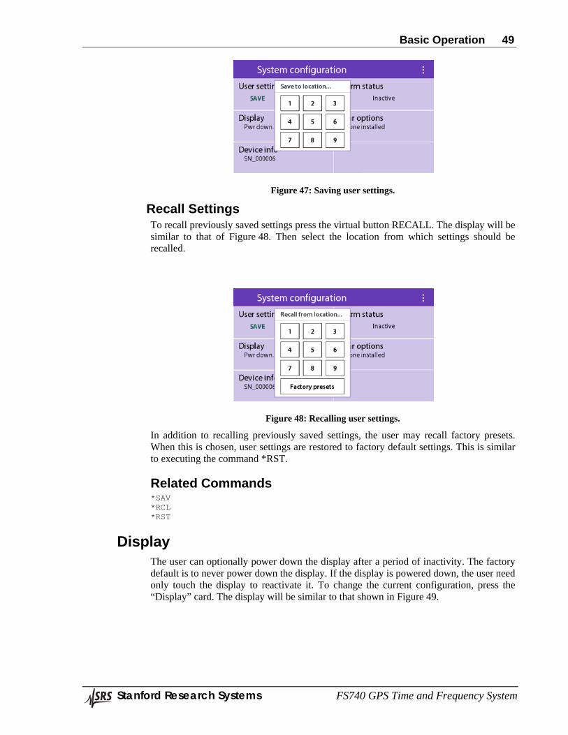
Basic Operation 49
Stanford Research Systems FS740 GPS Time and Frequency System
Figure 47: Saving user settings.
Recall Settings To recall previously saved settings press the virtual button RECALL. The display will be similar to that of Figure 48. Then select the location from which settings should be recalled.
Figure 48: Recalling user settings.
In addition to recalling previously saved settings, the user may recall factory presets. When this is chosen, user settings are restored to factory default settings. This is similar to executing the command *RST.
Related Commands *SAV *RCL *RST
Display The user can optionally power down the display after a period of inactivity. The factory default is to never power down the display. If the display is powered down, the user need only touch the display to reactivate it. To change the current configuration, press the “Display” card. The display will be similar to that shown in Figure 49.
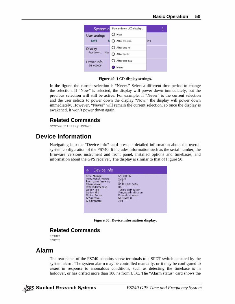
Basic Operation 50
Stanford Research Systems FS740 GPS Time and Frequency System
Figure 49: LCD display settings.
In the figure, the current selection is “Never.” Select a different time period to change the selection. If “Now” is selected, the display will power down immediately, but the previous selection will still be active. For example, if “Never” is the current selection and the user selects to power down the display “Now,” the display will power down immediately. However, “Never” will remain the current selection, so once the display is awakened, it won’t power down again.
Related Commands SYSTem:DISPlay:POWer
Device Information Navigating into the “Device info” card presents detailed information about the overall system configuration of the FS740. It includes information such as the serial number, the firmware versions instrument and front panel, installed options and timebases, and information about the GPS receiver. The display is similar to that of Figure 50.
Figure 50: Device information display.
Related Commands *IDN? *OPT?
Alarm The rear panel of the FS740 contains screw terminals to a SPDT switch actuated by the system alarm. The system alarm may be controlled manually, or it may be configured to assert in response to anomalous conditions, such as detecting the timebase is in holdover, or has drifted more than 100 ns from UTC. The “Alarm status” card shows the
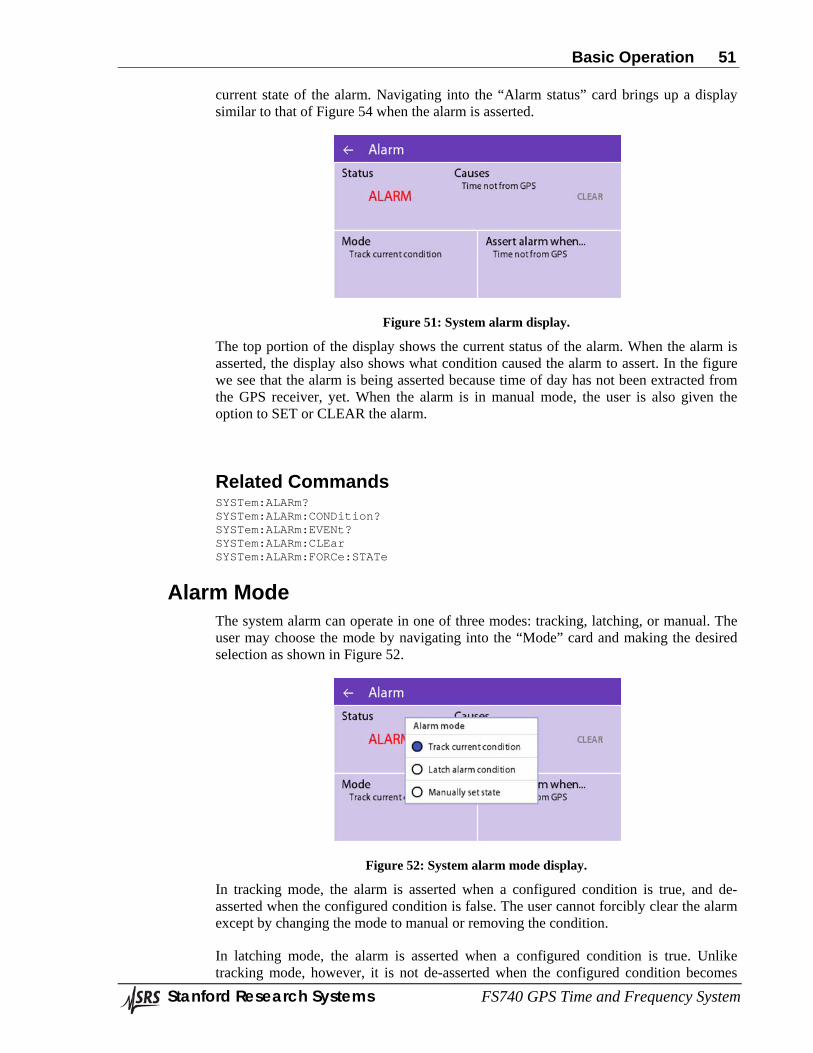
Basic Operation 51
Stanford Research Systems FS740 GPS Time and Frequency System
current state of the alarm. Navigating into the “Alarm status” card brings up a display similar to that of Figure 54 when the alarm is asserted.
Figure 51: System alarm display.
The top portion of the display shows the current status of the alarm. When the alarm is asserted, the display also shows what condition caused the alarm to assert. In the figure we see that the alarm is being asserted because time of day has not been extracted from the GPS receiver, yet. When the alarm is in manual mode, the user is also given the option to SET or CLEAR the alarm.
Related Commands SYSTem:ALARm? SYSTem:ALARm:CONDition? SYSTem:ALARm:EVENt? SYSTem:ALARm:CLEar SYSTem:ALARm:FORCe:STATe
Alarm Mode The system alarm can operate in one of three modes: tracking, latching, or manual. The user may choose the mode by navigating into the “Mode” card and making the desired selection as shown in Figure 52.
Figure 52: System alarm mode display.
In tracking mode, the alarm is asserted when a configured condition is true, and de-asserted when the configured condition is false. The user cannot forcibly clear the alarm except by changing the mode to manual or removing the condition.
In latching mode, the alarm is asserted when a configured condition is true. Unlike tracking mode, however, it is not de-asserted when the configured condition becomes
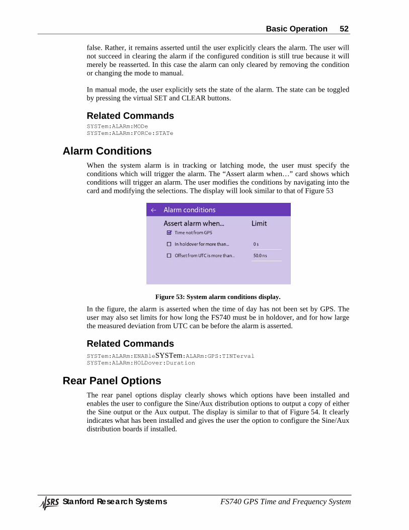
Basic Operation 52
Stanford Research Systems FS740 GPS Time and Frequency System
false. Rather, it remains asserted until the user explicitly clears the alarm. The user will not succeed in clearing the alarm if the configured condition is still true because it will merely be reasserted. In this case the alarm can only cleared by removing the condition or changing the mode to manual.
In manual mode, the user explicitly sets the state of the alarm. The state can be toggled by pressing the virtual SET and CLEAR buttons.
Related Commands SYSTem:ALARm:MODe SYSTem:ALARm:FORCe:STATe
Alarm Conditions When the system alarm is in tracking or latching mode, the user must specify the conditions which will trigger the alarm. The “Assert alarm when…” card shows which conditions will trigger an alarm. The user modifies the conditions by navigating into the card and modifying the selections. The display will look similar to that of Figure 53
Figure 53: System alarm conditions display.
In the figure, the alarm is asserted when the time of day has not been set by GPS. The user may also set limits for how long the FS740 must be in holdover, and for how large the measured deviation from UTC can be before the alarm is asserted.
Related Commands SYSTem:ALARm:ENABleSYSTem:ALARm:GPS:TINTerval SYSTem:ALARm:HOLDover:Duration
Rear Panel Options The rear panel options display clearly shows which options have been installed and enables the user to configure the Sine/Aux distribution options to output a copy of either the Sine output or the Aux output. The display is similar to that of Figure 54. It clearly indicates what has been installed and gives the user the option to configure the Sine/Aux distribution boards if installed.
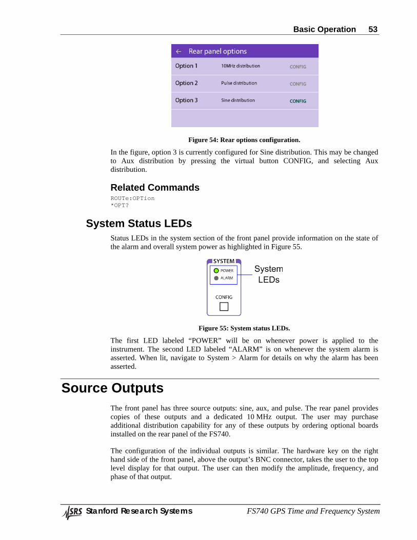
Basic Operation 53
Stanford Research Systems FS740 GPS Time and Frequency System
Figure 54: Rear options configuration.
In the figure, option 3 is currently configured for Sine distribution. This may be changed to Aux distribution by pressing the virtual button CONFIG, and selecting Aux distribution.
Related Commands ROUTe:OPTion *OPT?
System Status LEDs Status LEDs in the system section of the front panel provide information on the state of the alarm and overall system power as highlighted in Figure 55.
Figure 55: System status LEDs.
The first LED labeled “POWER” will be on whenever power is applied to the instrument. The second LED labeled “ALARM” is on whenever the system alarm is asserted. When lit, navigate to System > Alarm for details on why the alarm has been asserted.
Source Outputs The front panel has three source outputs: sine, aux, and pulse. The rear panel provides copies of these outputs and a dedicated 10 MHz output. The user may purchase additional distribution capability for any of these outputs by ordering optional boards installed on the rear panel of the FS740.
The configuration of the individual outputs is similar. The hardware key on the right hand side of the front panel, above the output’s BNC connector, takes the user to the top level display for that output. The user can then modify the amplitude, frequency, and phase of that output.
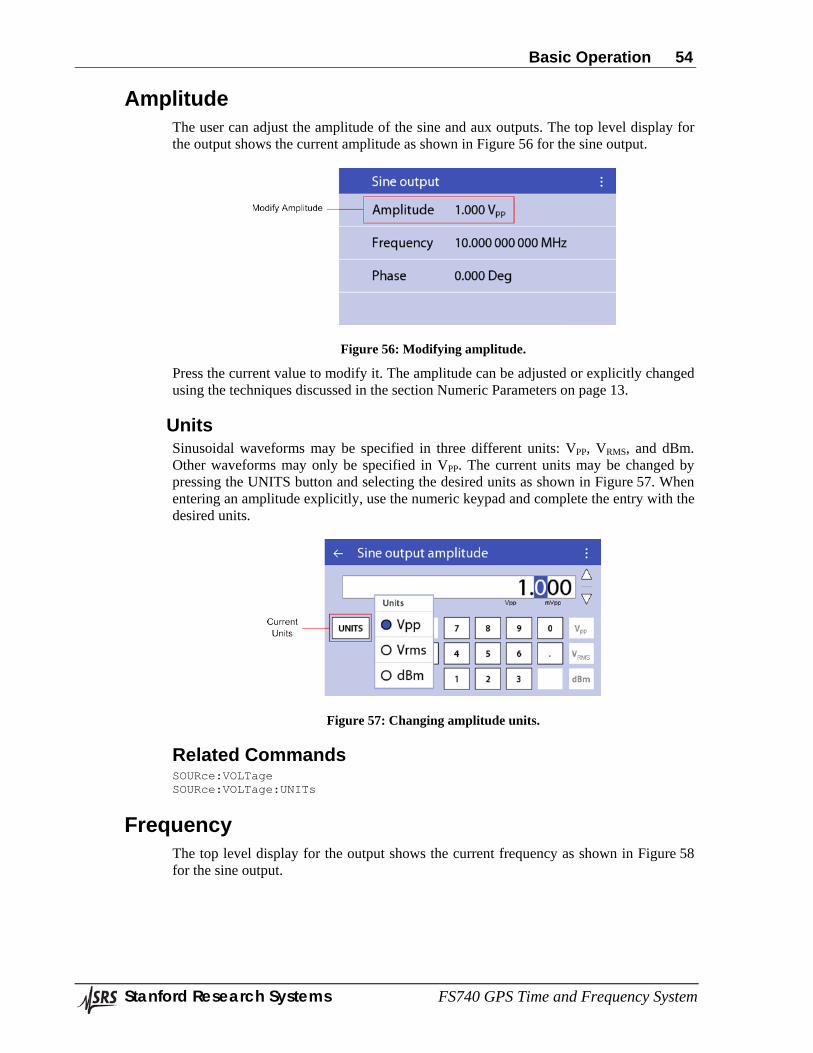
Basic Operation 54
Stanford Research Systems FS740 GPS Time and Frequency System
Amplitude The user can adjust the amplitude of the sine and aux outputs. The top level display for the output shows the current amplitude as shown in Figure 56 for the sine output.
Figure 56: Modifying amplitude.
Press the current value to modify it. The amplitude can be adjusted or explicitly changed using the techniques discussed in the section Numeric Parameters on page 13.
Units Sinusoidal waveforms may be specified in three different units: VPP, VRMS, and dBm. Other waveforms may only be specified in VPP. The current units may be changed by pressing the UNITS button and selecting the desired units as shown in Figure 57. When entering an amplitude explicitly, use the numeric keypad and complete the entry with the desired units.
Figure 57: Changing amplitude units.
Related Commands SOURce:VOLTage SOURce:VOLTage:UNITs
Frequency The top level display for the output shows the current frequency as shown in Figure 58 for the sine output.
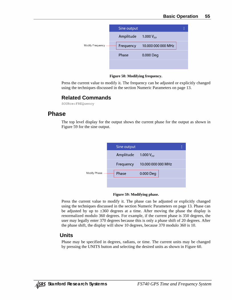
Basic Operation 55
Stanford Research Systems FS740 GPS Time and Frequency System
Figure 58: Modifying frequency.
Press the current value to modify it. The frequency can be adjusted or explicitly changed using the techniques discussed in the section Numeric Parameters on page 13.
Related Commands SOURce:FREQuency
Phase The top level display for the output shows the current phase for the output as shown in Figure 59 for the sine output.
Figure 59: Modifying phase.
Press the current value to modify it. The phase can be adjusted or explicitly changed using the techniques discussed in the section Numeric Parameters on page 13. Phase can be adjusted by up to ±360 degrees at a time. After moving the phase the display is renormalized modulo 360 degrees. For example, if the current phase is 350 degrees, the user may legally enter 370 degrees because this is only a phase shift of 20 degrees. After the phase shift, the display will show 10 degrees, because 370 modulo 360 is 10.
Units Phase may be specified in degrees, radians, or time. The current units may be changed by pressing the UNITS button and selecting the desired units as shown in Figure 60.
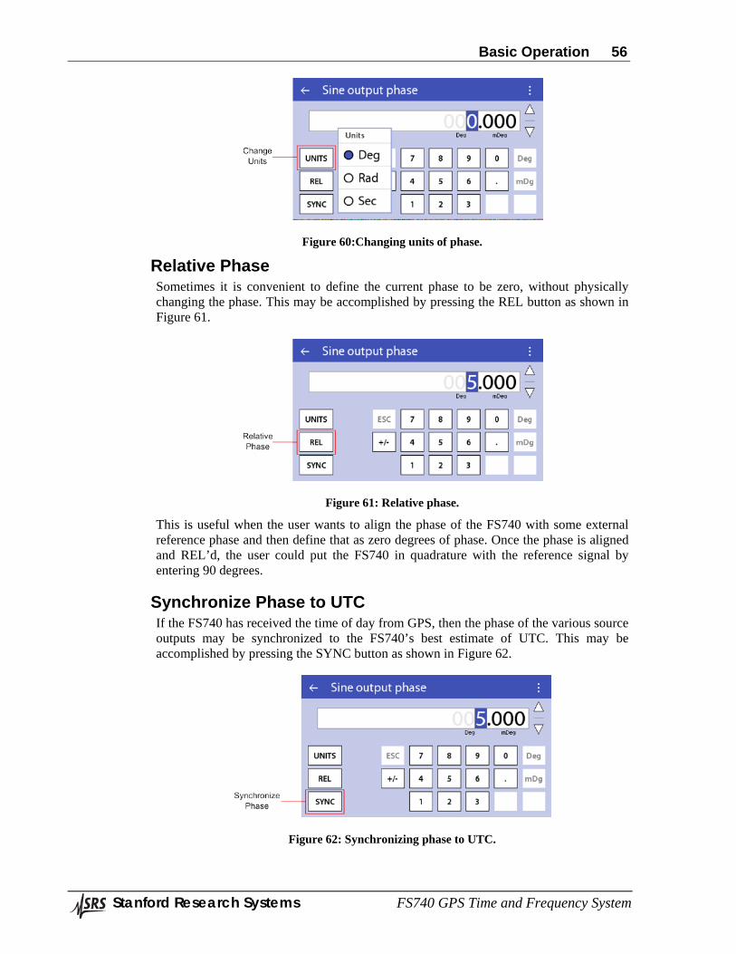
Basic Operation 56
Stanford Research Systems FS740 GPS Time and Frequency System
Figure 60:Changing units of phase.
Relative Phase Sometimes it is convenient to define the current phase to be zero, without physically changing the phase. This may be accomplished by pressing the REL button as shown in Figure 61.
Figure 61: Relative phase.
This is useful when the user wants to align the phase of the FS740 with some external reference phase and then define that as zero degrees of phase. Once the phase is aligned and REL’d, the user could put the FS740 in quadrature with the reference signal by entering 90 degrees.
Synchronize Phase to UTC If the FS740 has received the time of day from GPS, then the phase of the various source outputs may be synchronized to the FS740’s best estimate of UTC. This may be accomplished by pressing the SYNC button as shown in Figure 62.
Figure 62: Synchronizing phase to UTC.
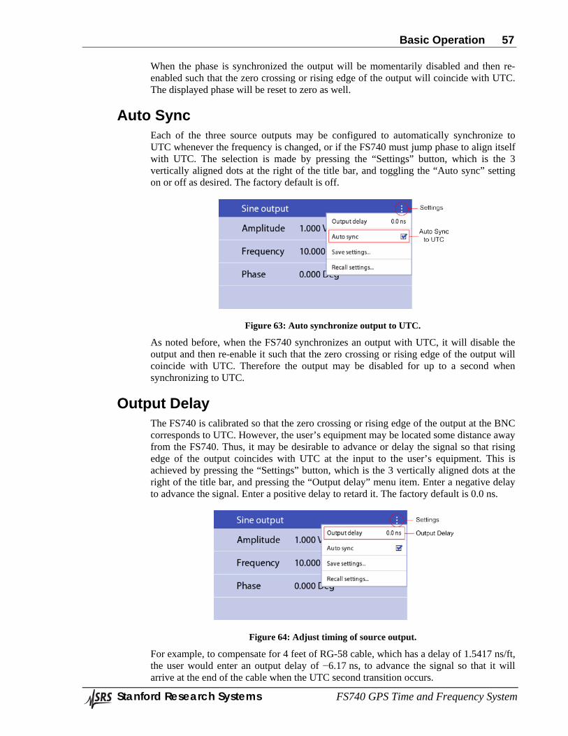
Basic Operation 57
Stanford Research Systems FS740 GPS Time and Frequency System
When the phase is synchronized the output will be momentarily disabled and then re-enabled such that the zero crossing or rising edge of the output will coincide with UTC. The displayed phase will be reset to zero as well.
Auto Sync Each of the three source outputs may be configured to automatically synchronize to UTC whenever the frequency is changed, or if the FS740 must jump phase to align itself with UTC. The selection is made by pressing the “Settings” button, which is the 3 vertically aligned dots at the right of the title bar, and toggling the “Auto sync” setting on or off as desired. The factory default is off.
Figure 63: Auto synchronize output to UTC.
As noted before, when the FS740 synchronizes an output with UTC, it will disable the output and then re-enable it such that the zero crossing or rising edge of the output will coincide with UTC. Therefore the output may be disabled for up to a second when synchronizing to UTC.
Output Delay The FS740 is calibrated so that the zero crossing or rising edge of the output at the BNC corresponds to UTC. However, the user’s equipment may be located some distance away from the FS740. Thus, it may be desirable to advance or delay the signal so that rising edge of the output coincides with UTC at the input to the user’s equipment. This is achieved by pressing the “Settings” button, which is the 3 vertically aligned dots at the right of the title bar, and pressing the “Output delay” menu item. Enter a negative delay to advance the signal. Enter a positive delay to retard it. The factory default is 0.0 ns.
Figure 64: Adjust timing of source output.
For example, to compensate for 4 feet of RG-58 cable, which has a delay of 1.5417 ns/ft, the user would enter an output delay of −6.17 ns, to advance the signal so that it will arrive at the end of the cable when the UTC second transition occurs.
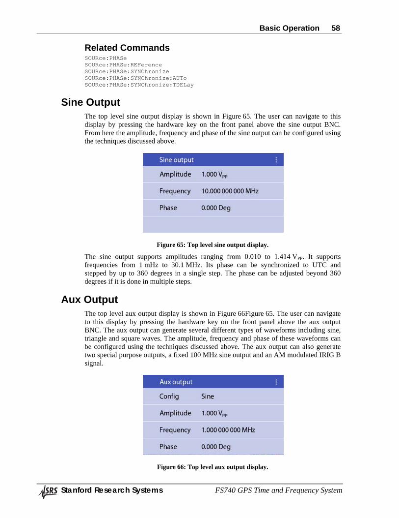
Basic Operation 58
Stanford Research Systems FS740 GPS Time and Frequency System
Related Commands SOURce:PHASe SOURce:PHASe:REFerence SOURce:PHASe:SYNChronize SOURce:PHASe:SYNChronize:AUTo SOURce:PHASe:SYNChronize:TDELay
Sine Output The top level sine output display is shown in Figure 65. The user can navigate to this display by pressing the hardware key on the front panel above the sine output BNC. From here the amplitude, frequency and phase of the sine output can be configured using the techniques discussed above.
Figure 65: Top level sine output display.
The sine output supports amplitudes ranging from 0.010 to 1.414 VPP. It supports frequencies from 1 mHz to 30.1 MHz. Its phase can be synchronized to UTC and stepped by up to 360 degrees in a single step. The phase can be adjusted beyond 360 degrees if it is done in multiple steps.
Aux Output The top level aux output display is shown in Figure 66Figure 65. The user can navigate to this display by pressing the hardware key on the front panel above the aux output BNC. The aux output can generate several different types of waveforms including sine, triangle and square waves. The amplitude, frequency and phase of these waveforms can be configured using the techniques discussed above. The aux output can also generate two special purpose outputs, a fixed 100 MHz sine output and an AM modulated IRIG B signal.
Figure 66: Top level aux output display.
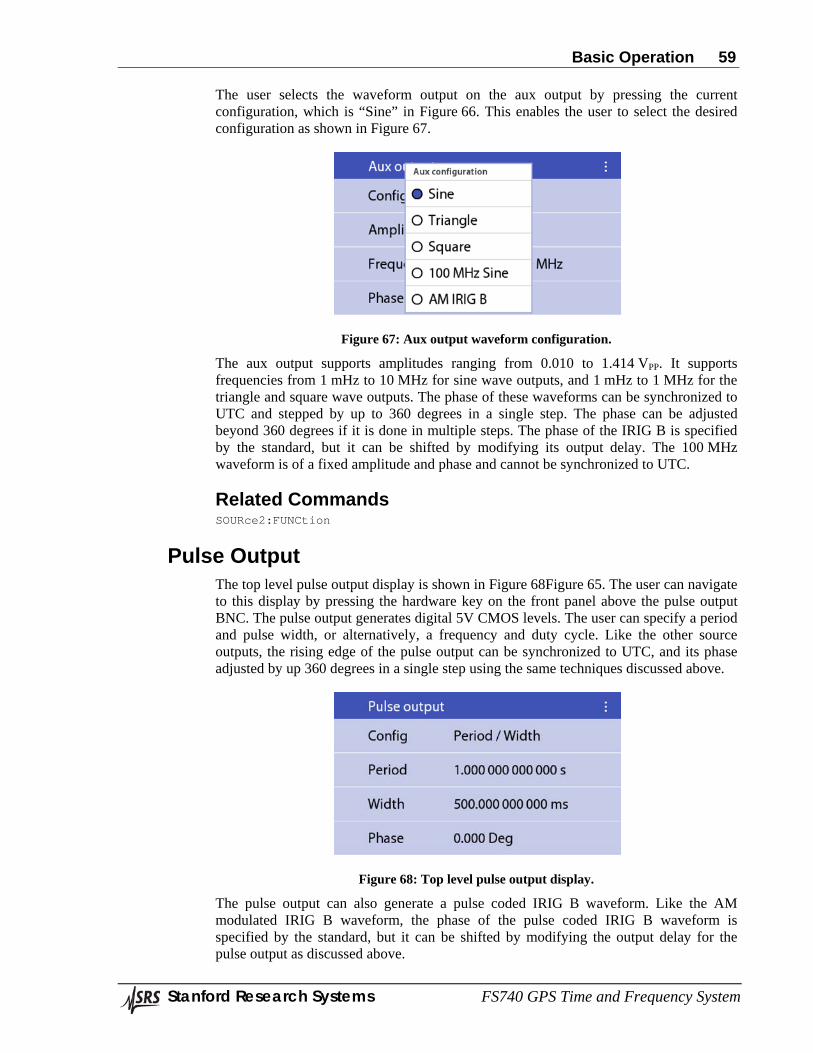
Basic Operation 59
Stanford Research Systems FS740 GPS Time and Frequency System
The user selects the waveform output on the aux output by pressing the current configuration, which is “Sine” in Figure 66. This enables the user to select the desired configuration as shown in Figure 67.
Figure 67: Aux output waveform configuration.
The aux output supports amplitudes ranging from 0.010 to 1.414 VPP. It supports frequencies from 1 mHz to 10 MHz for sine wave outputs, and 1 mHz to 1 MHz for the triangle and square wave outputs. The phase of these waveforms can be synchronized to UTC and stepped by up to 360 degrees in a single step. The phase can be adjusted beyond 360 degrees if it is done in multiple steps. The phase of the IRIG B is specified by the standard, but it can be shifted by modifying its output delay. The 100 MHz waveform is of a fixed amplitude and phase and cannot be synchronized to UTC.
Related Commands SOURce2:FUNCtion
Pulse Output The top level pulse output display is shown in Figure 68Figure 65. The user can navigate to this display by pressing the hardware key on the front panel above the pulse output BNC. The pulse output generates digital 5V CMOS levels. The user can specify a period and pulse width, or alternatively, a frequency and duty cycle. Like the other source outputs, the rising edge of the pulse output can be synchronized to UTC, and its phase adjusted by up 360 degrees in a single step using the same techniques discussed above.
Figure 68: Top level pulse output display.
The pulse output can also generate a pulse coded IRIG B waveform. Like the AM modulated IRIG B waveform, the phase of the pulse coded IRIG B waveform is specified by the standard, but it can be shifted by modifying the output delay for the pulse output as discussed above.
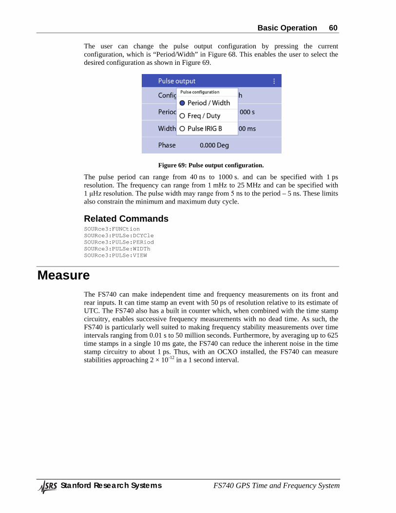
Basic Operation 60
Stanford Research Systems FS740 GPS Time and Frequency System
The user can change the pulse output configuration by pressing the current configuration, which is “Period/Width” in Figure 68. This enables the user to select the desired configuration as shown in Figure 69.
Figure 69: Pulse output configuration.
The pulse period can range from 40 ns to 1000 s. and can be specified with 1 ps resolution. The frequency can range from 1 mHz to 25 MHz and can be specified with 1 μHz resolution. The pulse width may range from 5 ns to the period – 5 ns. These limits also constrain the minimum and maximum duty cycle.
Related Commands SOURce3:FUNCtion SOURce3:PULSe:DCYCle SOURce3:PULSe:PERiod SOURce3:PULSe:WIDTh SOURce3:PULSe:VIEW
Measure The FS740 can make independent time and frequency measurements on its front and rear inputs. It can time stamp an event with 50 ps of resolution relative to its estimate of UTC. The FS740 also has a built in counter which, when combined with the time stamp circuitry, enables successive frequency measurements with no dead time. As such, the FS740 is particularly well suited to making frequency stability measurements over time intervals ranging from 0.01 s to 50 million seconds. Furthermore, by averaging up to 625 time stamps in a single 10 ms gate, the FS740 can reduce the inherent noise in the time stamp circuitry to about 1 ps. Thus, with an OCXO installed, the FS740 can measure stabilities approaching 2 × 10-12 in a 1 second interval.
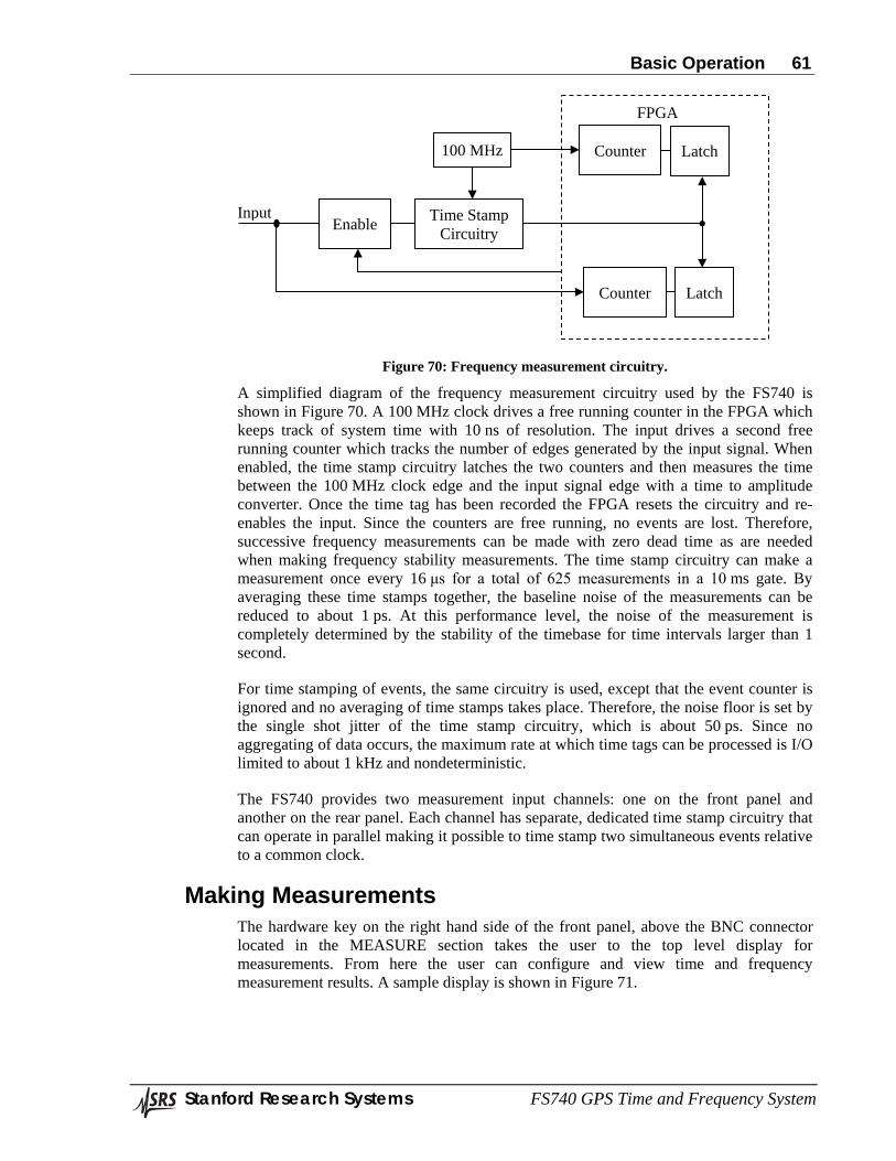
Basic Operation 61
Stanford Research Systems FS740 GPS Time and Frequency System
Figure 70: Frequency measurement circuitry.
A simplified diagram of the frequency measurement circuitry used by the FS740 is shown in Figure 70. A 100 MHz clock drives a free running counter in the FPGA which keeps track of system time with 10 ns of resolution. The input drives a second free running counter which tracks the number of edges generated by the input signal. When enabled, the time stamp circuitry latches the two counters and then measures the time between the 100 MHz clock edge and the input signal edge with a time to amplitude converter. Once the time tag has been recorded the FPGA resets the circuitry and re-enables the input. Since the counters are free running, no events are lost. Therefore, successive frequency measurements can be made with zero dead time as are needed when making frequency stability measurements. The time stamp circuitry can make a measurement once every 16 μs for a total of 625 measurements in a 10 ms gate. By averaging these time stamps together, the baseline noise of the measurements can be reduced to about 1 ps. At this performance level, the noise of the measurement is completely determined by the stability of the timebase for time intervals larger than 1 second.
For time stamping of events, the same circuitry is used, except that the event counter is ignored and no averaging of time stamps takes place. Therefore, the noise floor is set by the single shot jitter of the time stamp circuitry, which is about 50 ps. Since no aggregating of data occurs, the maximum rate at which time tags can be processed is I/O limited to about 1 kHz and nondeterministic.
The FS740 provides two measurement input channels: one on the front panel and another on the rear panel. Each channel has separate, dedicated time stamp circuitry that can operate in parallel making it possible to time stamp two simultaneous events relative to a common clock.
Making Measurements The hardware key on the right hand side of the front panel, above the BNC connector located in the MEASURE section takes the user to the top level display for measurements. From here the user can configure and view time and frequency measurement results. A sample display is shown in Figure 71.
Time Stamp Circuitry Enable
FPGA
Input
Counter Latch
100 MHz Counter Latch
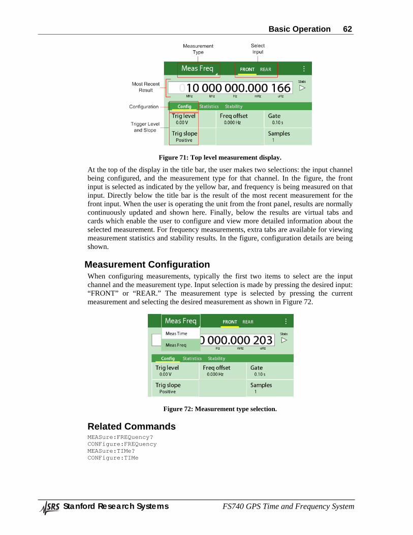
Basic Operation 62
Stanford Research Systems FS740 GPS Time and Frequency System
Figure 71: Top level measurement display.
At the top of the display in the title bar, the user makes two selections: the input channel being configured, and the measurement type for that channel. In the figure, the front input is selected as indicated by the yellow bar, and frequency is being measured on that input. Directly below the title bar is the result of the most recent measurement for the front input. When the user is operating the unit from the front panel, results are normally continuously updated and shown here. Finally, below the results are virtual tabs and cards which enable the user to configure and view more detailed information about the selected measurement. For frequency measurements, extra tabs are available for viewing measurement statistics and stability results. In the figure, configuration details are being shown.
Measurement Configuration When configuring measurements, typically the first two items to select are the input channel and the measurement type. Input selection is made by pressing the desired input: “FRONT” or “REAR.” The measurement type is selected by pressing the current measurement and selecting the desired measurement as shown in Figure 72.
Figure 72: Measurement type selection.
Related Commands MEASure:FREQuency? CONFigure:FREQuency MEASure:TIMe? CONFigure:TIMe
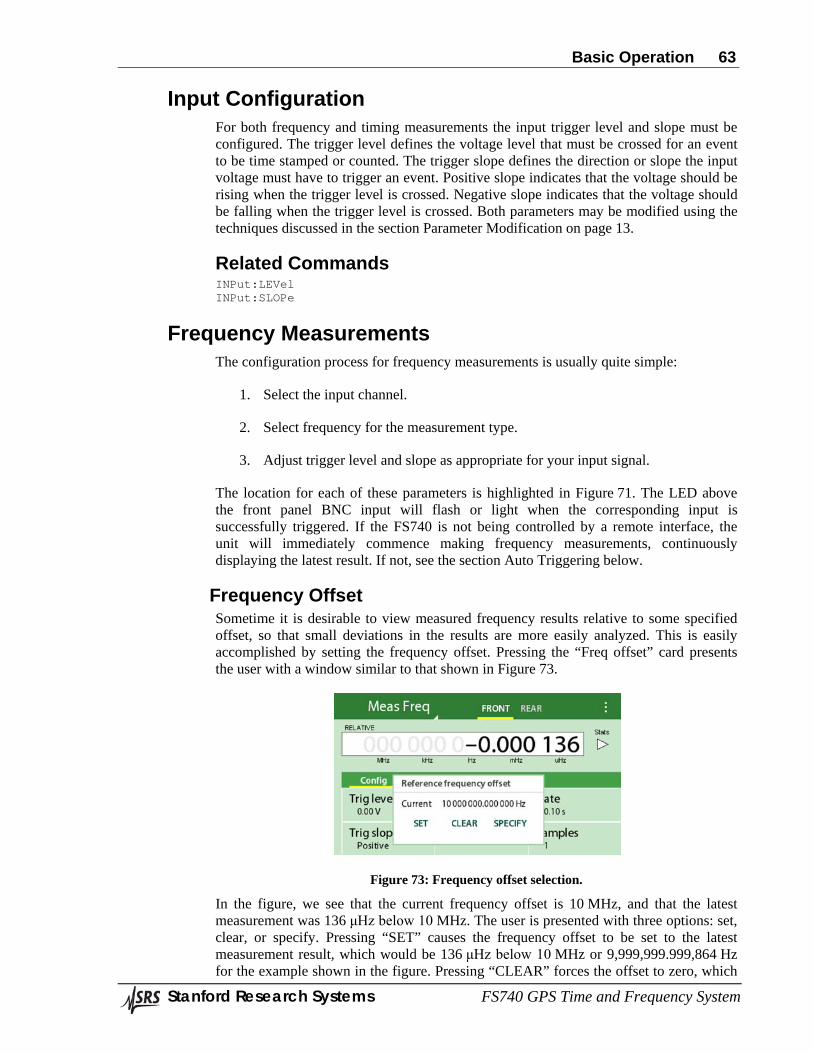
Basic Operation 63
Stanford Research Systems FS740 GPS Time and Frequency System
Input Configuration For both frequency and timing measurements the input trigger level and slope must be configured. The trigger level defines the voltage level that must be crossed for an event to be time stamped or counted. The trigger slope defines the direction or slope the input voltage must have to trigger an event. Positive slope indicates that the voltage should be rising when the trigger level is crossed. Negative slope indicates that the voltage should be falling when the trigger level is crossed. Both parameters may be modified using the techniques discussed in the section Parameter Modification on page 13.
Related Commands INPut:LEVel INPut:SLOPe
Frequency Measurements The configuration process for frequency measurements is usually quite simple:
1. Select the input channel.
2. Select frequency for the measurement type.
3. Adjust trigger level and slope as appropriate for your input signal.
The location for each of these parameters is highlighted in Figure 71. The LED above the front panel BNC input will flash or light when the corresponding input is successfully triggered. If the FS740 is not being controlled by a remote interface, the unit will immediately commence making frequency measurements, continuously displaying the latest result. If not, see the section Auto Triggering below.
Frequency Offset Sometime it is desirable to view measured frequency results relative to some specified offset, so that small deviations in the results are more easily analyzed. This is easily accomplished by setting the frequency offset. Pressing the “Freq offset” card presents the user with a window similar to that shown in Figure 73.
Figure 73: Frequency offset selection.
In the figure, we see that the current frequency offset is 10 MHz, and that the latest measurement was 136 μHz below 10 MHz. The user is presented with three options: set, clear, or specify. Pressing “SET” causes the frequency offset to be set to the latest measurement result, which would be 136 μHz below 10 MHz or 9,999,999.999,864 Hz for the example shown in the figure. Pressing “CLEAR” forces the offset to zero, which
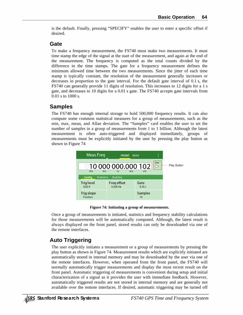
Basic Operation 64
Stanford Research Systems FS740 GPS Time and Frequency System
is the default. Finally, pressing “SPECIFY” enables the user to enter a specific offset if desired.
Gate To make a frequency measurement, the FS740 must make two measurements. It must time stamp the edge of the signal at the start of the measurement, and again at the end of the measurement. The frequency is computed as the total counts divided by the difference in the time stamps. The gate for a frequency measurement defines the minimum allowed time between the two measurements. Since the jitter of each time stamp is typically constant, the resolution of the measurement generally increases or decreases in proportion to the gate interval. For the default gate interval of 0.1 s, the FS740 can generally provide 11 digits of resolution. This increases to 12 digits for a 1 s gate, and decreases to 10 digits for a 0.01 s gate. The FS740 accepts gate intervals from 0.01 s to 1000 s.
Samples The FS740 has enough internal storage to hold 500,000 frequency results. It can also compute some common statistical measures for a group of measurements, such as the min, max, mean, and Allan deviation. The “Samples” card enables the user to set the number of samples in a group of measurements from 1 to 1 billion. Although the latest measurement is often auto-triggered and displayed immediately, groups of measurements must be explicitly initiated by the user by pressing the play button as shown in Figure 74
Figure 74: Initiating a group of measurements.
Once a group of measurements is initiated, statistics and frequency stability calculations for those measurements will be automatically computed. Although, the latest result is always displayed on the front panel, stored results can only be downloaded via one of the remote interfaces.
Auto Triggering The user explicitly initiates a measurement or a group of measurements by pressing the play button as shown in Figure 74. Measurement results which are explicitly initiated are automatically stored in internal memory and may be downloaded by the user via one of the remote interfaces. However, when operated from the front panel, the FS740 will normally automatically trigger measurements and display the most recent result on the front panel. Automatic triggering of measurements is convenient during setup and initial characterization of a signal as it provides the user with immediate feedback. However, automatically triggered results are not stored in internal memory and are generally not available over the remote interfaces. If desired, automatic triggering may be turned off
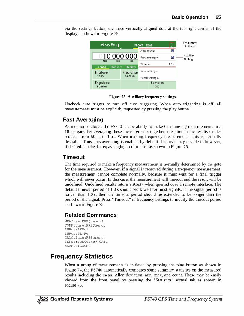
Basic Operation 65
Stanford Research Systems FS740 GPS Time and Frequency System
via the settings button, the three vertically aligned dots at the top right corner of the display, as shown in Figure 75.
Figure 75: Auxiliary frequency settings.
Uncheck auto trigger to turn off auto triggering. When auto triggering is off, all measurements must be explicitly requested by pressing the play button.
Fast Averaging As mentioned above, the FS740 has be ability to make 625 time tag measurements in a 10 ms gate. By averaging these measurements together, the jitter in the results can be reduced from 50 ps to 1 ps. When making frequency measurements, this is normally desirable. Thus, this averaging is enabled by default. The user may disable it, however, if desired. Uncheck freq averaging to turn it off as shown in Figure 75.
Timeout The time required to make a frequency measurement is normally determined by the gate for the measurement. However, if a signal is removed during a frequency measurement, the measurement cannot complete normally, because it must wait for a final trigger which will never occur. In this case, the measurement will timeout and the result will be undefined. Undefined results return 9.91e37 when queried over a remote interface. The default timeout period of 1.0 s should work well for most signals. If the signal period is longer than 1.0 s, then the timeout period should be extended to be longer than the period of the signal. Press “Timeout” in frequency settings to modify the timeout period as shown in Figure 75.
Related Commands MEASure:FREQuency? CONFigure:FREQuency INPut:LEVel INPut:SLOPe CALCulate:REFerence SENSe:FREQuency:GATE SAMPle:COUNt
Frequency Statistics When a group of measurements is initiated by pressing the play button as shown in Figure 74, the FS740 automatically computes some summary statistics on the measured results including the mean, Allan deviation, min, max, and count. These may be easily viewed from the front panel by pressing the “Statistics” virtual tab as shown in Figure 76.
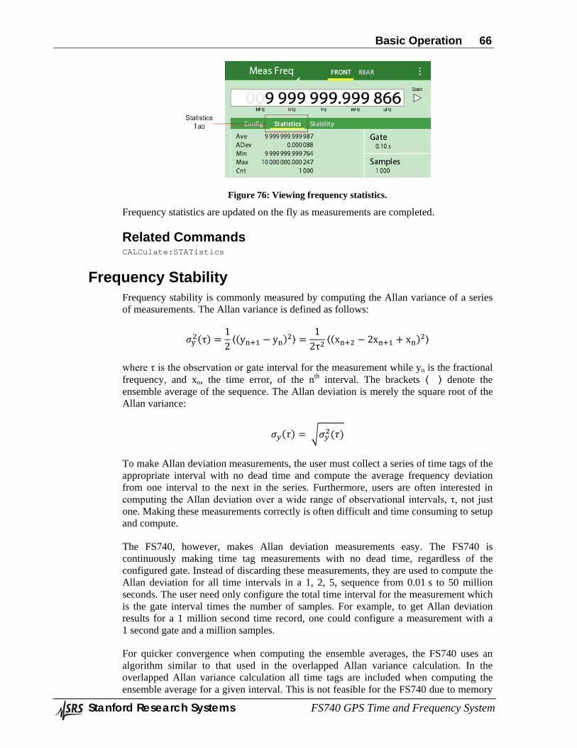
Basic Operation 66
Stanford Research Systems FS740 GPS Time and Frequency System
Figure 76: Viewing frequency statistics.
Frequency statistics are updated on the fly as measurements are completed.
Related Commands CALCulate:STATistics
Frequency Stability Frequency stability is commonly measured by computing the Allan variance of a series of measurements. The Allan variance is defined as follows:
𝜎y2(τ) =12⟨(yn+1 − yn)2⟩ =
12τ2
⟨(xn+2 − 2xn+1 + xn)2⟩
where τ is the observation or gate interval for the measurement while yn is the fractional frequency, and xn, the time error, of the nth interval. The brackets ⟨ ⟩ denote the ensemble average of the sequence. The Allan deviation is merely the square root of the Allan variance:
𝜎𝑦(𝜏) = 𝜎𝑦2(𝜏)
To make Allan deviation measurements, the user must collect a series of time tags of the appropriate interval with no dead time and compute the average frequency deviation from one interval to the next in the series. Furthermore, users are often interested in computing the Allan deviation over a wide range of observational intervals, τ, not just one. Making these measurements correctly is often difficult and time consuming to setup and compute.
The FS740, however, makes Allan deviation measurements easy. The FS740 is continuously making time tag measurements with no dead time, regardless of the configured gate. Instead of discarding these measurements, they are used to compute the Allan deviation for all time intervals in a 1, 2, 5, sequence from 0.01 s to 50 million seconds. The user need only configure the total time interval for the measurement which is the gate interval times the number of samples. For example, to get Allan deviation results for a 1 million second time record, one could configure a measurement with a 1 second gate and a million samples.
For quicker convergence when computing the ensemble averages, the FS740 uses an algorithm similar to that used in the overlapped Allan variance calculation. In the overlapped Allan variance calculation all time tags are included when computing the ensemble average for a given interval. This is not feasible for the FS740 due to memory
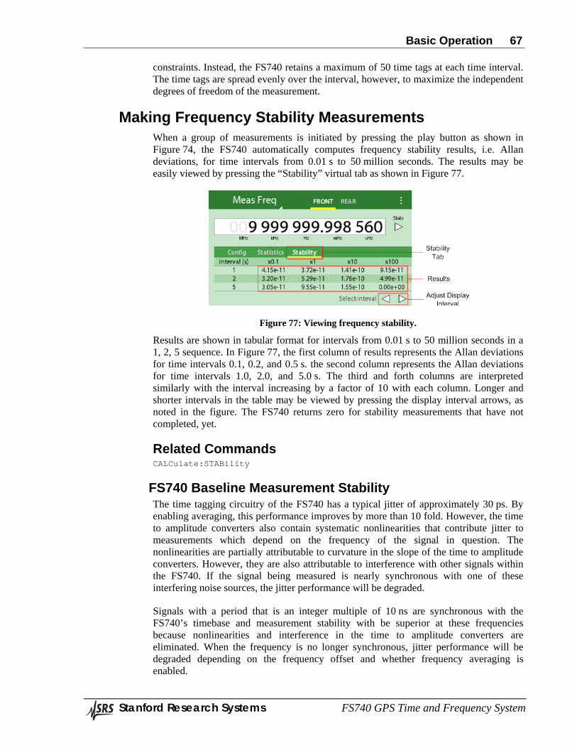
Basic Operation 67
Stanford Research Systems FS740 GPS Time and Frequency System
constraints. Instead, the FS740 retains a maximum of 50 time tags at each time interval. The time tags are spread evenly over the interval, however, to maximize the independent degrees of freedom of the measurement.
Making Frequency Stability Measurements When a group of measurements is initiated by pressing the play button as shown in Figure 74, the FS740 automatically computes frequency stability results, i.e. Allan deviations, for time intervals from 0.01 s to 50 million seconds. The results may be easily viewed by pressing the “Stability” virtual tab as shown in Figure 77.
Figure 77: Viewing frequency stability.
Results are shown in tabular format for intervals from 0.01 s to 50 million seconds in a 1, 2, 5 sequence. In Figure 77, the first column of results represents the Allan deviations for time intervals 0.1, 0.2, and 0.5 s. the second column represents the Allan deviations for time intervals 1.0, 2.0, and 5.0 s. The third and forth columns are interpreted similarly with the interval increasing by a factor of 10 with each column. Longer and shorter intervals in the table may be viewed by pressing the display interval arrows, as noted in the figure. The FS740 returns zero for stability measurements that have not completed, yet.
Related Commands CALCulate:STABility
FS740 Baseline Measurement Stability The time tagging circuitry of the FS740 has a typical jitter of approximately 30 ps. By enabling averaging, this performance improves by more than 10 fold. However, the time to amplitude converters also contain systematic nonlinearities that contribute jitter to measurements which depend on the frequency of the signal in question. The nonlinearities are partially attributable to curvature in the slope of the time to amplitude converters. However, they are also attributable to interference with other signals within the FS740. If the signal being measured is nearly synchronous with one of these interfering noise sources, the jitter performance will be degraded.
Signals with a period that is an integer multiple of 10 ns are synchronous with the FS740’s timebase and measurement stability with be superior at these frequencies because nonlinearities and interference in the time to amplitude converters are eliminated. When the frequency is no longer synchronous, jitter performance will be degraded depending on the frequency offset and whether frequency averaging is enabled.
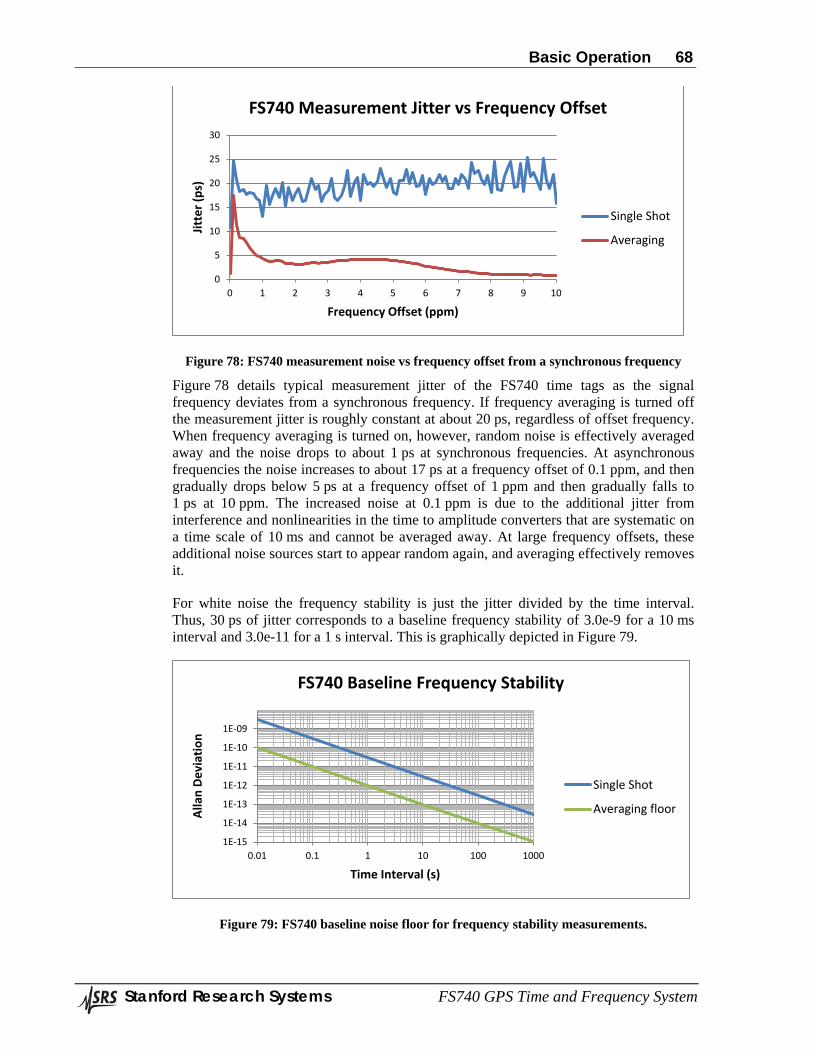
Basic Operation 68
Stanford Research Systems FS740 GPS Time and Frequency System
Figure 78: FS740 measurement noise vs frequency offset from a synchronous frequency
Figure 78 details typical measurement jitter of the FS740 time tags as the signal frequency deviates from a synchronous frequency. If frequency averaging is turned off the measurement jitter is roughly constant at about 20 ps, regardless of offset frequency. When frequency averaging is turned on, however, random noise is effectively averaged away and the noise drops to about 1 ps at synchronous frequencies. At asynchronous frequencies the noise increases to about 17 ps at a frequency offset of 0.1 ppm, and then gradually drops below 5 ps at a frequency offset of 1 ppm and then gradually falls to 1 ps at 10 ppm. The increased noise at 0.1 ppm is due to the additional jitter from interference and nonlinearities in the time to amplitude converters that are systematic on a time scale of 10 ms and cannot be averaged away. At large frequency offsets, these additional noise sources start to appear random again, and averaging effectively removes it.
For white noise the frequency stability is just the jitter divided by the time interval. Thus, 30 ps of jitter corresponds to a baseline frequency stability of 3.0e-9 for a 10 ms interval and 3.0e-11 for a 1 s interval. This is graphically depicted in Figure 79.
Figure 79: FS740 baseline noise floor for frequency stability measurements.
0
5
10
15
20
25
30
0 1 2 3 4 5 6 7 8 9 10
Jitte
r (ps
)
Frequency Offset (ppm)
FS740 Measurement Jitter vs Frequency Offset
Single Shot
Averaging
1E-15
1E-14
1E-13
1E-12
1E-11
1E-10
1E-09
0.01 0.1 1 10 100 1000
Alla
n De
viat
ion
Time Interval (s)
FS740 Baseline Frequency Stability
Single Shot
Averaging floor
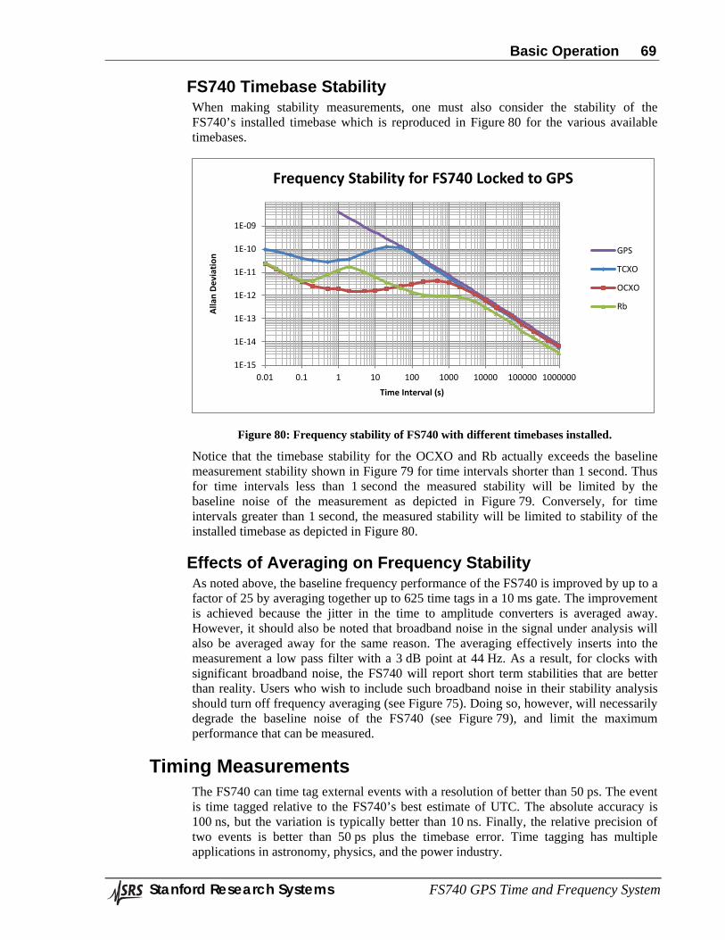
Basic Operation 69
Stanford Research Systems FS740 GPS Time and Frequency System
FS740 Timebase Stability When making stability measurements, one must also consider the stability of the FS740’s installed timebase which is reproduced in Figure 80 for the various available timebases.
Figure 80: Frequency stability of FS740 with different timebases installed.
Notice that the timebase stability for the OCXO and Rb actually exceeds the baseline measurement stability shown in Figure 79 for time intervals shorter than 1 second. Thus for time intervals less than 1 second the measured stability will be limited by the baseline noise of the measurement as depicted in Figure 79. Conversely, for time intervals greater than 1 second, the measured stability will be limited to stability of the installed timebase as depicted in Figure 80.
Effects of Averaging on Frequency Stability As noted above, the baseline frequency performance of the FS740 is improved by up to a factor of 25 by averaging together up to 625 time tags in a 10 ms gate. The improvement is achieved because the jitter in the time to amplitude converters is averaged away. However, it should also be noted that broadband noise in the signal under analysis will also be averaged away for the same reason. The averaging effectively inserts into the measurement a low pass filter with a 3 dB point at 44 Hz. As a result, for clocks with significant broadband noise, the FS740 will report short term stabilities that are better than reality. Users who wish to include such broadband noise in their stability analysis should turn off frequency averaging (see Figure 75). Doing so, however, will necessarily degrade the baseline noise of the FS740 (see Figure 79), and limit the maximum performance that can be measured.
Timing Measurements The FS740 can time tag external events with a resolution of better than 50 ps. The event is time tagged relative to the FS740’s best estimate of UTC. The absolute accuracy is 100 ns, but the variation is typically better than 10 ns. Finally, the relative precision of two events is better than 50 ps plus the timebase error. Time tagging has multiple applications in astronomy, physics, and the power industry.
1E-15
1E-14
1E-13
1E-12
1E-11
1E-10
1E-09
0.01 0.1 1 10 100 1000 10000 100000 1000000
Alla
n De
viat
ion
Time Interval (s)
Frequency Stability for FS740 Locked to GPS
GPS
TCXO
OCXO
Rb
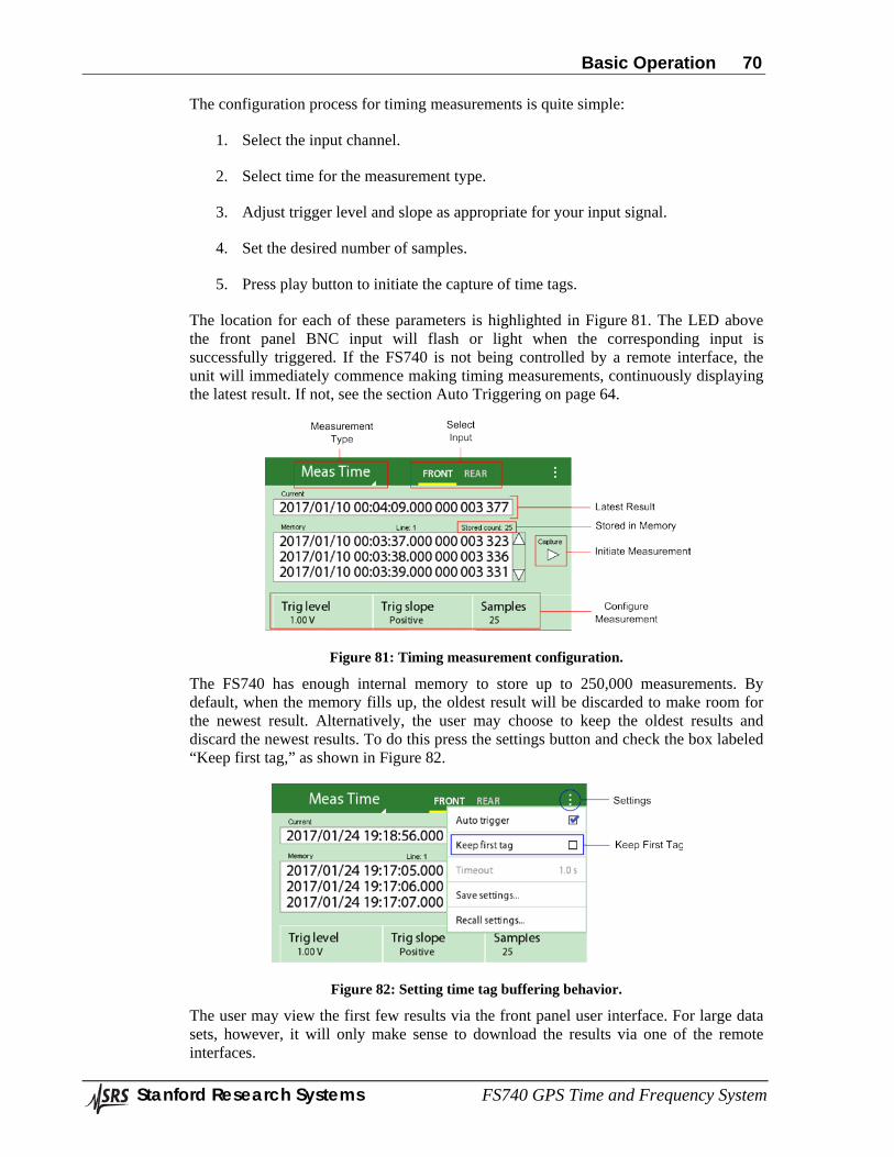
Basic Operation 70
Stanford Research Systems FS740 GPS Time and Frequency System
The configuration process for timing measurements is quite simple:
1. Select the input channel.
2. Select time for the measurement type.
3. Adjust trigger level and slope as appropriate for your input signal.
4. Set the desired number of samples.
5. Press play button to initiate the capture of time tags.
The location for each of these parameters is highlighted in Figure 81. The LED above the front panel BNC input will flash or light when the corresponding input is successfully triggered. If the FS740 is not being controlled by a remote interface, the unit will immediately commence making timing measurements, continuously displaying the latest result. If not, see the section Auto Triggering on page 64.
Figure 81: Timing measurement configuration.
The FS740 has enough internal memory to store up to 250,000 measurements. By default, when the memory fills up, the oldest result will be discarded to make room for the newest result. Alternatively, the user may choose to keep the oldest results and discard the newest results. To do this press the settings button and check the box labeled “Keep first tag,” as shown in Figure 82.
Figure 82: Setting time tag buffering behavior.
The user may view the first few results via the front panel user interface. For large data sets, however, it will only make sense to download the results via one of the remote interfaces.
Basic Operation 71
Stanford Research Systems FS740 GPS Time and Frequency System
Factory Default Settings The factory default settings for the FS740 are shown in Table 5. The settings are divided into two categories: system settings and user settings. User settings largely apply to the configuration of the source outputs and the measurement inputs. The user may force these parameters to their default settings by executing the *RST command or recalling factory presets via the front panel interface. These parameters are identified by a check mark at the far right of Table 5.
System settings, on the other hand, largely apply to the configuration of the timebase, GPS, communications parameters, and system alarms. They are unaffected by the execution of the *RST command or a recall of factory presets from the front panel. They are stored in nonvolatile memory and retain their configuration even when power is cycled. These parameters are generally intended to be set once and then left alone.
Table 5: Factory default settings
Parameter Value Set by *RST Display Timebase Display Display power down Never Sine frequency 10 MHz Sine amplitude 1 Vpp Sine amplitude units Vpp Sine phase 0 Degrees Sine phase units Degrees Sine phase auto sync Off Sine phase time delay 0 ps Aux waveform Sine wave Aux frequency 1 MHz Aux amplitude 1 Vpp Aux amplitude units Vpp Aux phase 0 Degrees Aux phase units Degrees Aux phase auto sync Off Aux phase time delay 0 ps Pulse waveform Pulse Pulse view Period/Width Pulse frequency 1 Hz Pulse duty cycle 50 % Pulse period 1 s Pulse width 500 ms Pulse phase 0 Degrees Pulse phase units Degrees Pulse phase auto sync Off Pulse phase time delay 0 ps Input level 0 V Input slope Positive Input measurement Frequency Input frequency offset 0 Hz Input frequency gate 0.1 s Input sample size 1
Basic Operation 72
Stanford Research Systems FS740 GPS Time and Frequency System
Input auto trigger On Input frequency averaging On Input time out 1 s Input time tag buffer mode Keep last Timebase GPS lock Enabled Timebase holdover mode Wait for good 1pps timing from
GPS
Timebase bandwidth mode Auto bandwidth control Timebase time interval limit 1 μs Timebase manual time constant 30 s GPS timing alignment UTC GPS timing quality Require 3 satellites GPS survey mode Redo survey at power on GPS position fixes in survey 2000 GPS antenna cable delay 0 ns Local time offset 0 hr RS-232 baud rate 115200 baud Ethernet speed 100 Base T TCP/IP configuration method DHCP TCP/IP static IP address 0.0.0.0 TCP/IP static subnet address 0.0.0.0 TCP/IP static gateway address 0.0.0.0 System alarm mode Manually set state System alarm manual state Off System alarm holdover duration limit
0 s
System alarm timing error limit 100 ns Option sin/aux routing Sine out
Forcing User Settings to Factory Defaults The user may easily force user settings to their factory default values from the front panel by pressing Settings > Recall Settings, and then choosing “Factory Presets”
Figure 83: Setting user settings to factory presets.
This is equivalent to executing the remote interface command *RST. It forces parameters in Table 5 with a check mark at the right to the default setting.
Related Commands *RST
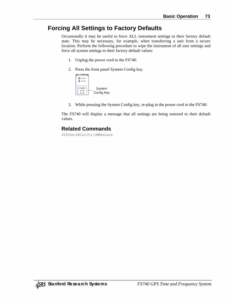
Basic Operation 73
Stanford Research Systems FS740 GPS Time and Frequency System
Forcing All Settings to Factory Defaults Occasionally it may be useful to force ALL instrument settings to their factory default state. This may be necessary, for example, when transferring a unit from a secure location. Perform the following procedure to wipe the instrument of all user settings and force all system settings to their factory default values:
1. Unplug the power cord to the FS740.
2. Press the front panel System Config key.
3. While pressing the System Config key, re-plug in the power cord to the FS740.
The FS740 will display a message that all settings are being restored to their default values.
Related Commands SYSTem:SECurity:IMMediate

Remote Programming 75
Stanford Research Systems FS740 GPS Time and Frequency System
Remote Programming
Introduction The FS740 may be programmed via remote interfaces included with the instrument. Any host computer interfaced to the instrument can easily control and monitor its operation. The front panel can even be locked out when necessary for complete computer control. This might be desirable as part of an automated test environment. The FS740 supports two standard remote interfaces: RS-232 and an Ethernet based local area network (LAN) interface which supports TCP/IP communication.
RS-232 An RS-232 communications port is included on the rear panel of the unit. The RS-232 interface connector is a standard 9 pin, type D, female connector configured as a DCE (transmit on pin 2, receive on pin 3). In order to communicate properly over RS-232, the instrument and the host computer both must be configured to use the same settings. The following baud rates are supported: 115200 (default), 57600, 38400, 19200, 9600, and 4800. The rest of the communication parameters are fixed at 8 data bits, 1 stop bit, no parity, and RTS/CTS hardware flow control. See section RS-232 Configuration on page 44 for details on how to configure the RS-232 port from the front panel.
Ethernet A rear panel RJ-45 connector may be used to connect the instrument to a 10/100 Base-T Ethernet LAN. In order to function properly on an Ethernet LAN, the unit needs to obtain a valid TCP/IP configuration, which includes an IP address, a subnet mask, and a default gateway or router address. The FS740 supports three methods for obtaining these parameters: DHCP for automatic IP configuration, Auto-IP for link local addressing, and Static IP for manual configuration. Check with your network administrator for the proper method of configuration of instruments on your network before attaching the FS740 to your network. See section TCP/IP Configuration on page 45 for details on how to select the proper method of TCP/IP configuration from the front panel.
Once connected to the network, the user can connect to the FS740 using one of the following protocols: telnet, bare TCP stream connections, and VXI-11.
Telnet The FS740 accepts telnet connections on port 5024. Telnet is useful for interactive sessions because it supports line based command execution with automatic echoing of typed characters. This enables users to easily type (and correct) commands manually from the keyboard. Telnet, however, should not be used for automated computer control, however, because the echoing of characters and processing of telnet commands will significantly complicate the endeavor.
Bare TCP The FS740 accepts bare TCP stream connections on port 5025. Bare TCP connections are ideal for automated computer control. All bytes are passed directly to the input queue
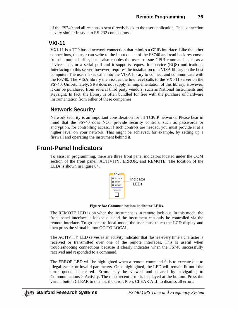
Remote Programming 76
Stanford Research Systems FS740 GPS Time and Frequency System
of the FS740 and all responses sent directly back to the user application. This connection is very similar in style to RS-232 connections.
VXI-11 VXI-11 is a TCP based network connection that mimics a GPIB interface. Like the other connections, the user can write to the input queue of the FS740 and read back responses from its output buffer, but it also enables the user to issue GPIB commands such as a device clear, or a serial poll and it supports request for service (RQS) notifications. Interfacing to this server, however, requires the installation of a VISA library on the host computer. The user makes calls into the VISA library to connect and communicate with the FS740. The VISA library then issues the low level calls to the VXI-11 server on the FS740. Unfortunately, SRS does not supply an implementation of this library. However, it can be purchased from several third party vendors, such as National Instruments and Keysight. In fact, the library is often bundled for free with the purchase of hardware instrumentation from either of these companies.
Network Security Network security is an important consideration for all TCP/IP networks. Please bear in mind that the FS740 does NOT provide security controls, such as passwords or encryption, for controlling access. If such controls are needed, you must provide it at a higher level on your network. This might be achieved, for example, by setting up a firewall and operating the instrument behind it.
Front-Panel Indicators To assist in programming, there are three front panel indicators located under the COM section of the front panel: ACTIVITY, ERROR, and REMOTE. The location of the LEDs is shown in Figure 84.
Figure 84: Communications indicator LEDs.
The REMOTE LED is on when the instrument is in remote lock out. In this mode, the front panel interface is locked out and the instrument can only be controlled via the remote interface. To go back to local mode, the user must touch the LCD display and then press the virtual button GO TO LOCAL.
The ACTIVITY LED serves as an activity indicator that flashes every time a character is received or transmitted over one of the remote interfaces. This is useful when troubleshooting connections because it clearly indicates when the FS740 successfully received and responded to a command.
The ERROR LED will be highlighted when a remote command fails to execute due to illegal syntax or invalid parameters. Once highlighted, the LED will remain lit until the error queue is cleared. Errors may be viewed and cleared by navigating to Communications > Activity. The most recent error is displayed at the bottom. Press the virtual button CLEAR to dismiss the error. Press CLEAR ALL to dismiss all errors.
Remote Programming 77
Stanford Research Systems FS740 GPS Time and Frequency System
SCPI Command Language The FS740 uses the SCPI (Standard Commands for Programmable Instruments) language for controlling the instrument over a remote interface. The SCPI language is an ASCII based command language that organizes functions into a hierarchical tree of commands with branches of the tree separated by colons.
SubSystems The base or root of the tree represents a subsystem of the instrument. Each succeeding branch of the tree subdivides the subsystem into related categories of functionality. The final branch of the tree identifies a command related to the subsystem that can be executed by the FS740. This structure facilitates understanding of the functions carried out by commands. As an example, consider the subset of the STATus subsystem shown below.
STATus: GPS: CONDition? ENABle ENABle? [:EVENt]? OPERation: CONDition? ENABle ENABle? [:EVENt]?
STATus is a subsystem of the FS740 and it is at the root of the tree. At the next level down, the STATus subsystem is divided into two branches: GPS and OPERation. Each of these categories is then further subdivided into four virtually identical commands: CONDition, ENABle, ENABle?, and [:EVENt]?. However, because of the hierarchical structure of the language, we can infer that the commands listed under the GPS branch refer to GPS receiver status, while those listed under OPERation carry out the same functions but refer to OPERation status rather than GPS status. Thus, the hierarchical structure of the commands aids in the understanding of the operations carried out by the individual commands.
Understanding Command Syntax SCPI commands often take one or more parameters which modify or identify the numerical value a variable should take. Some parameters are required. Others may be optional. Furthermore, the data types for each parameter may differ. Thus, for brevity, we need a set of conventions for defining commands which clearly identifies all the valid variations of the command without having the list each possibility separately. These conventions are set forth here.
An example command is illustrated below:
SOURce[1|2]:VOLTage[:LEVel] <voltage>|MINimum|MAXimum|DEFault
Remote Programming 78
Stanford Research Systems FS740 GPS Time and Frequency System
Keyword Case Keywords are defined with a mixture of upper-case and lower-case letters. The upper-case letters indicate the short or abbreviated version of the keyword. This is usually the first 3 or 4 letters of the keyword. The user may send either the short version or the entire long version of the keyword in their programs. The case of the letters sent to the FS740 does not matter. It is only used here to succinctly identify the two versions of the keyword. Thus, SOUR, source, and Sour are all acceptable forms of the keyword. Other forms, such as SOU, or SOURC, are not. Given the definition above, the following commands are all identical:
SOUR:VOLT MIN SOURCE:VOLTAGE MINIMUM SOUR:VOLTAGE MIN
Punctuation Used in Definitions The following punctuation is used to identify variations and options for the command:
• Braces ( ) enclose different parameter choices. The braces, themselves, are not sent with the command
• A vertical bar ( | ) separates alternative parameter choices for the command. In the example above, the choices are a <voltage> or one of the keywords: MINimum, MAXimum, or DEFault. The vertical bar is not sent with the command.
• Triangle brackets ( < > ) indicate that you must specify a numerical value. In the example above, <voltage> would be specified as a number. Thus, one could set the voltage using the following command: SOUR:VOLT 1.253. The triangle brackets are not sent with the command.
• Square brackets identify optional keywords or parameters in the command. Optional items may be omitted if desired. In such case a default value is normally substituted for the parameter. In the example above, the keyword LEVel is optional and may be omitted. Thus, the command SOUR:VOLT:LEVEL 1.253 is identical to the command that omits the keyword: SOUR:VOLT 1.253.
Numeric Suffix Some keywords can have a numeric suffix appended to the keyword. In the example SOURce may be followed with a 1 or 2. These suffixes identify multiple channels of the same subsystem. Thus, SOUR1 identifies channel 1, and SOUR2 identifies channel 2. The numeric suffix is optional and if omitted, channel 1 is assumed.
Examples Putting it all together, all of the following commands are valid given the example definition presented above.
SOUR:VOLT MIN SOUR2:VOLT DEFAULT SOURCE1:VOLTAGE 1.234 SOURCE:VOLT MAXIMUM
Remote Programming 79
Stanford Research Systems FS740 GPS Time and Frequency System
Queries Command queries are usually formed by appending a question mark ( ? ) to the command. To query the output voltage of channel 1, we use the following command: SOUR:VOLT?
Separators As mentioned above, a colon ( : ) separates the different keywords that make up a command. If a command takes a parameter, a space MUST separate the last keyword of a command and the first parameter of that command. If a command takes multiple parameters, they are separated from each other with a comma ( , ). Finally, a semicolon ( ; ) is used to separate multiple commands on the same line. If the following command is in the same subsystem as the preceding command then the subsystem is not repeated for the second command. Otherwise the command must be fully specified and preceded by a colon. Given the example command tree presented in section SubSystems above, the following commands are valid:
STAT:GPS:ENAB 1; EVENT? STAT:GPS:COND?; :STAT:OPER:COND?
In the first line, both ENABle and EVENt are in the same subsystem, STAT:GPS, so that portion of the command is omitted for the EVENt? query. However, the two condition queries are in different subsystems, so the operational condition query is preceded by a colon and fully specified on the command line.
When multiple queries, separated by semicolons, are made in a single command line, the responses from the individual queries are separated by a semicolon as well.
IEEE 488.2 Common Commands The IEEE 488.2 standard defines several common commands that nearly all instruments support. Common commands start with an asterisk ( * ) followed by three letters. Like with SCPI commands, a space MUST separate the command and any parameters which follow. Multiple common commands may executed in a single line by separating the commands with a semicolon ( ; ). An example is given below.
*RST; *OPC?
Parameter Types The SCPI language supports several different data types for use with command parameters.
Numeric Values Parameters that take numeric values accept all common decimal representations of numbers, including optional signs, decimal points, or scientific notation. Hexadecimal values specified with a prefix of 0x prefix as used in the C language are also accepted. If only certain values are allowed, numeric entries will be rounded to the nearest allowed value. The following examples are all valid numeric entries:
100 -123.456 +1.23456e2 -.456 0x64
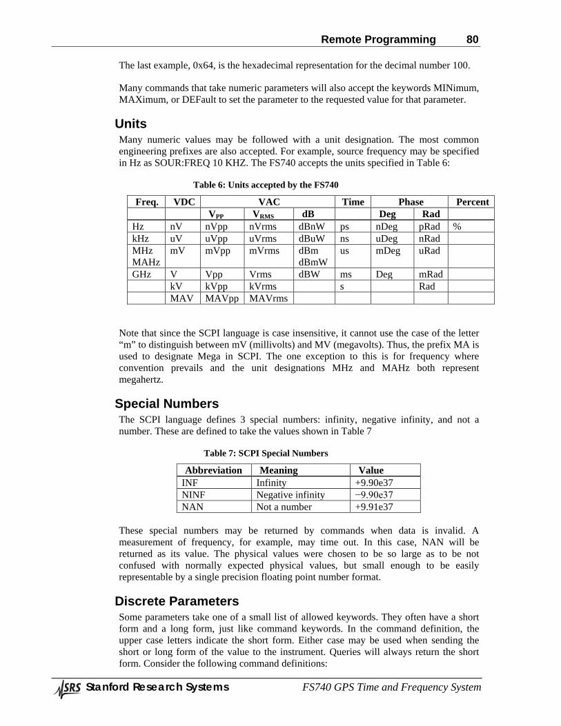
Remote Programming 80
Stanford Research Systems FS740 GPS Time and Frequency System
The last example, 0x64, is the hexadecimal representation for the decimal number 100.
Many commands that take numeric parameters will also accept the keywords MINimum, MAXimum, or DEFault to set the parameter to the requested value for that parameter.
Units Many numeric values may be followed with a unit designation. The most common engineering prefixes are also accepted. For example, source frequency may be specified in Hz as SOUR:FREQ 10 KHZ. The FS740 accepts the units specified in Table 6:
Table 6: Units accepted by the FS740
Freq. VDC VAC Time Phase Percent VPP VRMS dB Deg Rad
Hz nV nVpp nVrms dBnW ps nDeg pRad % kHz uV uVpp uVrms dBuW ns uDeg nRad MHz MAHz
mV mVpp mVrms dBm dBmW
us mDeg uRad
GHz V Vpp Vrms dBW ms Deg mRad kV kVpp kVrms s Rad MAV MAVpp MAVrms
Note that since the SCPI language is case insensitive, it cannot use the case of the letter “m” to distinguish between mV (millivolts) and MV (megavolts). Thus, the prefix MA is used to designate Mega in SCPI. The one exception to this is for frequency where convention prevails and the unit designations MHz and MAHz both represent megahertz.
Special Numbers The SCPI language defines 3 special numbers: infinity, negative infinity, and not a number. These are defined to take the values shown in Table 7
Table 7: SCPI Special Numbers
Abbreviation Meaning Value INF Infinity +9.90e37 NINF Negative infinity −9.90e37 NAN Not a number +9.91e37
These special numbers may be returned by commands when data is invalid. A measurement of frequency, for example, may time out. In this case, NAN will be returned as its value. The physical values were chosen to be so large as to be not confused with normally expected physical values, but small enough to be easily representable by a single precision floating point number format.
Discrete Parameters Some parameters take one of a small list of allowed keywords. They often have a short form and a long form, just like command keywords. In the command definition, the upper case letters indicate the short form. Either case may be used when sending the short or long form of the value to the instrument. Queries will always return the short form. Consider the following command definitions:
Remote Programming 81
Stanford Research Systems FS740 GPS Time and Frequency System
TBASe:CONFig:BWIDth [ AUTo | MANual ] TBASe:CONFig:BWIDth?
The user may specify auto bandwidth control by sending the command TBAS:CONF:BWID AUTO. The query will return AUT, which is the short form of the value.
String Parameters Quoted string parameters allow one to send almost any sequence of characters, including characters that are normally reserved as separator characters, such as a comma, semicolon, or colon. The string must begin and end with the same quote character: either a single quote, or a double quote. The quote delimiter may itself be included in the string if it is typed twice without any characters in between.
Command Termination Commands should be terminated with a line feed <LF>. They may optionally be terminated with a carriage return <CR> followed by a line feed <LF>. As previously noted, multiple commands may be sent in a single line if they separated by a semicolon ( ; ). Commands are executed in the order received and execution commences once the command separator or terminator is received.
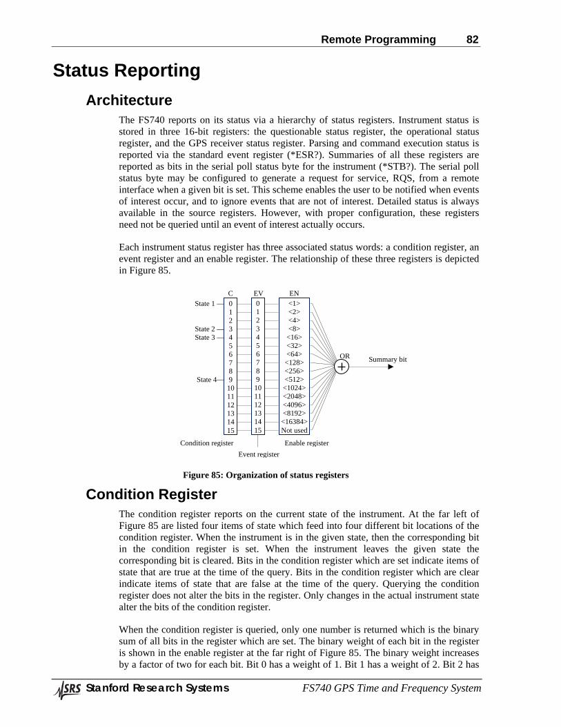
Remote Programming 82
Stanford Research Systems FS740 GPS Time and Frequency System
Status Reporting Architecture
The FS740 reports on its status via a hierarchy of status registers. Instrument status is stored in three 16-bit registers: the questionable status register, the operational status register, and the GPS receiver status register. Parsing and command execution status is reported via the standard event register (*ESR?). Summaries of all these registers are reported as bits in the serial poll status byte for the instrument (*STB?). The serial poll status byte may be configured to generate a request for service, RQS, from a remote interface when a given bit is set. This scheme enables the user to be notified when events of interest occur, and to ignore events that are not of interest. Detailed status is always available in the source registers. However, with proper configuration, these registers need not be queried until an event of interest actually occurs.
Each instrument status register has three associated status words: a condition register, an event register and an enable register. The relationship of these three registers is depicted in Figure 85.
Figure 85: Organization of status registers
Condition Register The condition register reports on the current state of the instrument. At the far left of Figure 85 are listed four items of state which feed into four different bit locations of the condition register. When the instrument is in the given state, then the corresponding bit in the condition register is set. When the instrument leaves the given state the corresponding bit is cleared. Bits in the condition register which are set indicate items of state that are true at the time of the query. Bits in the condition register which are clear indicate items of state that are false at the time of the query. Querying the condition register does not alter the bits in the register. Only changes in the actual instrument state alter the bits of the condition register.
When the condition register is queried, only one number is returned which is the binary sum of all bits in the register which are set. The binary weight of each bit in the register is shown in the enable register at the far right of Figure 85. The binary weight increases by a factor of two for each bit. Bit 0 has a weight of 1. Bit 1 has a weight of 2. Bit 2 has
Condition register Event register
Enable register
EN EV C 0 1 2 3 4 5 6 7 8 9 10 11 12 13 14 15
State 1 —
State 2 — State 3 —
State 4—
0 1 2 3 4 5 6 7 8 9 10 11 12 13 14 15
<1> <2> <4> <8>
<16> <32> <64> <128> <256> <512> <1024> <2048> <4096> <8192>
<16384> Not used
OR Summary bit
Remote Programming 83
Stanford Research Systems FS740 GPS Time and Frequency System
a weight of 4, and so on up to bit 14 which has a weight of 16384. The number returned by a query of the condition register is the sum of weights of the bits which are set.
For example, in Figure 85, State 1 feeds into bit 0 and State 2 feeds into bit 3. If both State 1 and State 2 are true, then both bits 0 and 3 will be set. If all other states are false, then the number returned by a query of the condition register will be the binary sum of bit 0 and bit 3, which is 1 + 8 = 9. If only State 2 is true, then only bit 3 will be set and a query of the condition register will return 8. Similarly, if only State 1 is true, then only bit 0 will be set and the query will return 1. Finally, if none of the states is true, the query will return 0.
Event Register Bits from the condition register feed into corresponding bits in the event register. The event register differs from the condition register, however, in that the bits are sticky. Once a bit is set, it remains set until explicitly cleared by a query of the event register. The event register, therefore, enables the user to capture all events that have occurred since the previous query of the register, even if the states in question are short lived and not true at the moment of the query.
Like the condition register, a query of the event register returns a single number which is the binary sum of all bits in the register which are set. (See the discussion of the condition register above for a detailed explanation of this process.)
Unlike the condition register, a query of the event register clears any bits which were previously set. Executing the *CLS command will also clear this register. Of course if corresponding bits in the condition register are still set, these bits will immediately be set again after the clear from the query.
Enable Register The enable register is a mask register that controls which bits from the event register will set the overall summary bit. If a bit in the enable register is set, then the corresponding bit in the event register will be combined with other enabled bits of the event register via a logical OR operation to create an overall summary bit.
The user sets the enable register with a single number which is the binary sum of all bits in the register which should be set. (See the discussion of the condition register above for a detailed explanation of this process.) Continuing with the example from Figure 85, If the enable register is set to 9 = 1 + 8, then the summary bit will be set if either bit 0 or bit 3 of the event register is set. Therefore, if the user detects that the summary bit is set, he can infer that either State 1 or State 2 or both were at least momentarily true since the last query of the event register.
Enable bits are set via a command. They are not cleared by a query or the execution of the *CLS command. To clear enabled bits, the user must send another set command with those bits set to zero. Sending the number zero will clear all bits of the enable register and prevent the summary bit from ever being set.
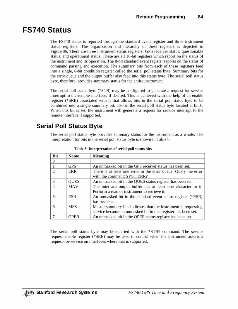
Remote Programming 84
Stanford Research Systems FS740 GPS Time and Frequency System
FS740 Status The FS740 status is reported through the standard event register and three instrument status registers. The organization and hierarchy of these registers is depicted in Figure 86. There are three instrument status registers: GPS receiver status, questionable status, and operational status. These are all 16-bit registers which report on the status of the instrument and its operation. The 8-bit standard event register reports on the status of command parsing and execution. The summary bits from each of these registers feed into a single, 8-bit condition register called the serial poll status byte. Summary bits for the error queue and the output buffer also feed into this status byte. The serial poll status byte, therefore, provides summary status for the entire instrument.
The serial poll status byte (*STB) may be configured to generate a request for service interrupt to the remote interface, if desired. This is achieved with the help of an enable register (*SRE) associated with it that allows bits in the serial poll status byte to be combined into a single summary bit, also in the serial poll status byte located at bit 6. When this bit is set, the instrument will generate a request for service interrupt to the remote interface if supported.
Serial Poll Status Byte The serial poll status byte provides summary status for the instrument as a whole. The interpretation for bits in the serial poll status byte is shown in Table 8.
Table 8: Interpretation of serial poll status bits
Bit Name Meaning 0 1 GPS An unmasked bit in the GPS receiver status has been set. 2 ERR There is at least one error in the error queue. Query the error
with the command SYST:ERR? 3 QUES An unmasked bit in the QUES status register has been set. 4 MAV The interface output buffer has at least one character in it.
Perform a read of instrument to retrieve it. 5 ESR An unmasked bit in the standard event status register (*ESR)
has been set. 6 MSS Master summary bit. Indicates that the instrument is requesting
service because an unmasked bit in this register has been set. 7 OPER An unmasked bit in the OPER status register has been set.
The serial poll status byte may be queried with the *STB? command. The service request enable register (*SRE) may be used to control when the instrument asserts a request-for-service on interfaces where that is supported.
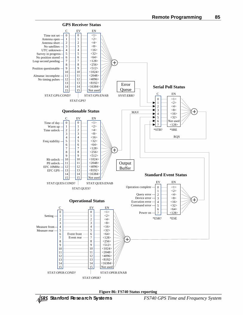
Remote Programming 85
Stanford Research Systems FS740 GPS Time and Frequency System
Figure 86: FS740 Status reporting
Operational Status
GPS Receiver Status
Questionable Status
Standard Event Status
Output Buffer
Serial Poll Status
0 1 2 3 4 5 6 7 8 9 10 11 12 13 14 15
Time not set — Antenna open — Antenna short —
No satellites — UTC unknown—
Survey in progress— No position stored —
Leap second pending —
Position questionable —
Almanac incomplete — No timing pulses —
0 1 2 3 4 5 6 7 8 9 10 11 12 13 14 15
<1> <2> <4> <8>
<16> <32> <64> <128> <256> <512> <1024> <2048> <4096> <8192>
<16384> Not used
EN EV C
STAT:GPS:COND? STAT:GPS?
STAT:GPS:ENAB
EN EV C 0 1 2 3 4 5 6 7 8 9 10 11 12 13 14 15
Time of day — Warm up —
Time unlock —
Freq stability —
Rb unlock — Pll unlock —
EFC 10MHz —EFC GPS —
0 1 2 3 4 5 6 7 8 9 10 11 12 13 14 15
<1> <2> <4> <8>
<16> <32> <64> <128> <256> <512> <1024> <2048> <4096> <8192>
<16384> Not used
STAT:QUES:COND? STAT:QUES?
STAT:QUES:ENAB
Error Queue
SYST:ERR?
0 1 2 3 4 5 6 7 8 9 10 11 12 13 14 15
Setting —
Measure front— Measure rear —
0 1 2 3 4 5 6 7 8 9 10 11 12 13 14 15
<1> <2> <4> <8>
<16> <32> <64> <128> <256> <512> <1024> <2048> <4096> <8192>
<16384> Not used
Event front Event rear
EN EV C
STAT:OPER:COND? STAT:OPER?
STAT:OPER:ENAB
0 1 2 3 4 5 6 7
Operation complete —
Query error — Device error —
Execution error — Command error —
Power on —
<1> <2> <4> <8>
<16> <32> <64> <128>
EN EV
*ESR? *ESE
0 1 2 3 4 5 6 7
<1> <2> <4> <8>
<16> <32>
Not used <128>
EN C
*STB? *SRE
RQS
MAV
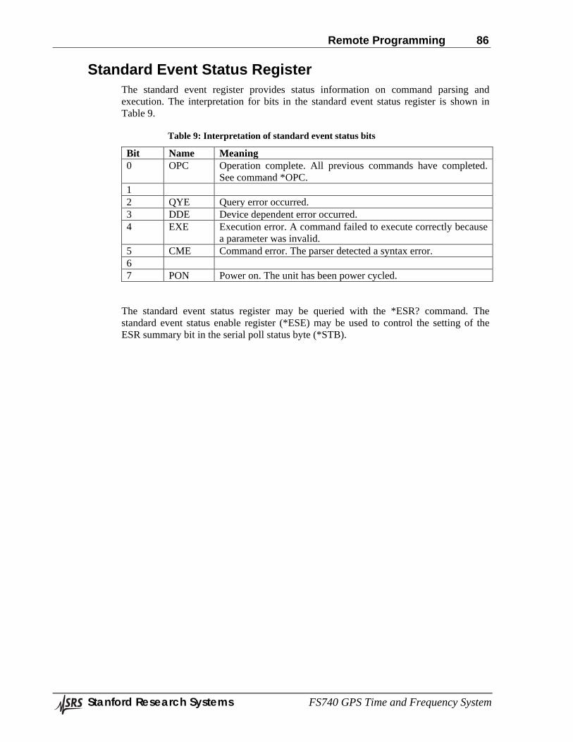
Remote Programming 86
Stanford Research Systems FS740 GPS Time and Frequency System
Standard Event Status Register The standard event register provides status information on command parsing and execution. The interpretation for bits in the standard event status register is shown in Table 9.
Table 9: Interpretation of standard event status bits
Bit Name Meaning 0 OPC Operation complete. All previous commands have completed.
See command *OPC. 1 2 QYE Query error occurred. 3 DDE Device dependent error occurred. 4 EXE Execution error. A command failed to execute correctly because
a parameter was invalid. 5 CME Command error. The parser detected a syntax error. 6 7 PON Power on. The unit has been power cycled.
The standard event status register may be queried with the *ESR? command. The standard event status enable register (*ESE) may be used to control the setting of the ESR summary bit in the serial poll status byte (*STB).
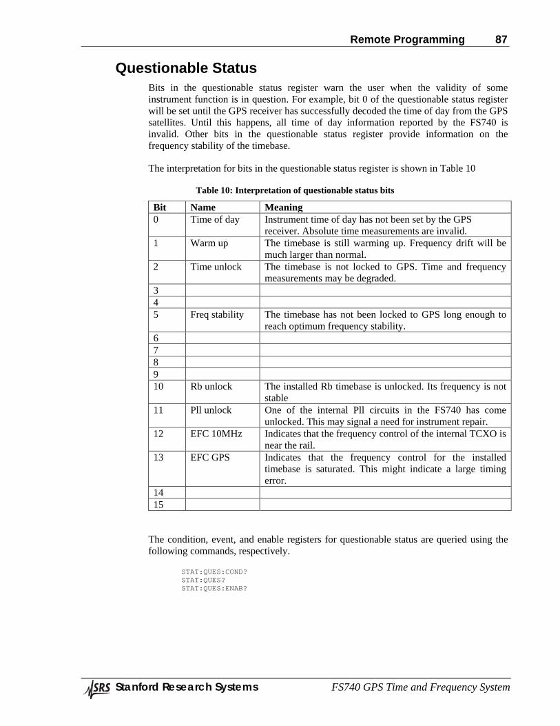
Remote Programming 87
Stanford Research Systems FS740 GPS Time and Frequency System
Questionable Status Bits in the questionable status register warn the user when the validity of some instrument function is in question. For example, bit 0 of the questionable status register will be set until the GPS receiver has successfully decoded the time of day from the GPS satellites. Until this happens, all time of day information reported by the FS740 is invalid. Other bits in the questionable status register provide information on the frequency stability of the timebase.
The interpretation for bits in the questionable status register is shown in Table 10
Table 10: Interpretation of questionable status bits
Bit Name Meaning 0 Time of day Instrument time of day has not been set by the GPS
receiver. Absolute time measurements are invalid. 1 Warm up The timebase is still warming up. Frequency drift will be
much larger than normal. 2 Time unlock The timebase is not locked to GPS. Time and frequency
measurements may be degraded. 3 4 5 Freq stability The timebase has not been locked to GPS long enough to
reach optimum frequency stability. 6 7 8 9 10 Rb unlock The installed Rb timebase is unlocked. Its frequency is not
stable 11 Pll unlock One of the internal Pll circuits in the FS740 has come
unlocked. This may signal a need for instrument repair. 12 EFC 10MHz Indicates that the frequency control of the internal TCXO is
near the rail. 13 EFC GPS Indicates that the frequency control for the installed
timebase is saturated. This might indicate a large timing error.
14 15
The condition, event, and enable registers for questionable status are queried using the following commands, respectively.
STAT:QUES:COND? STAT:QUES? STAT:QUES:ENAB?
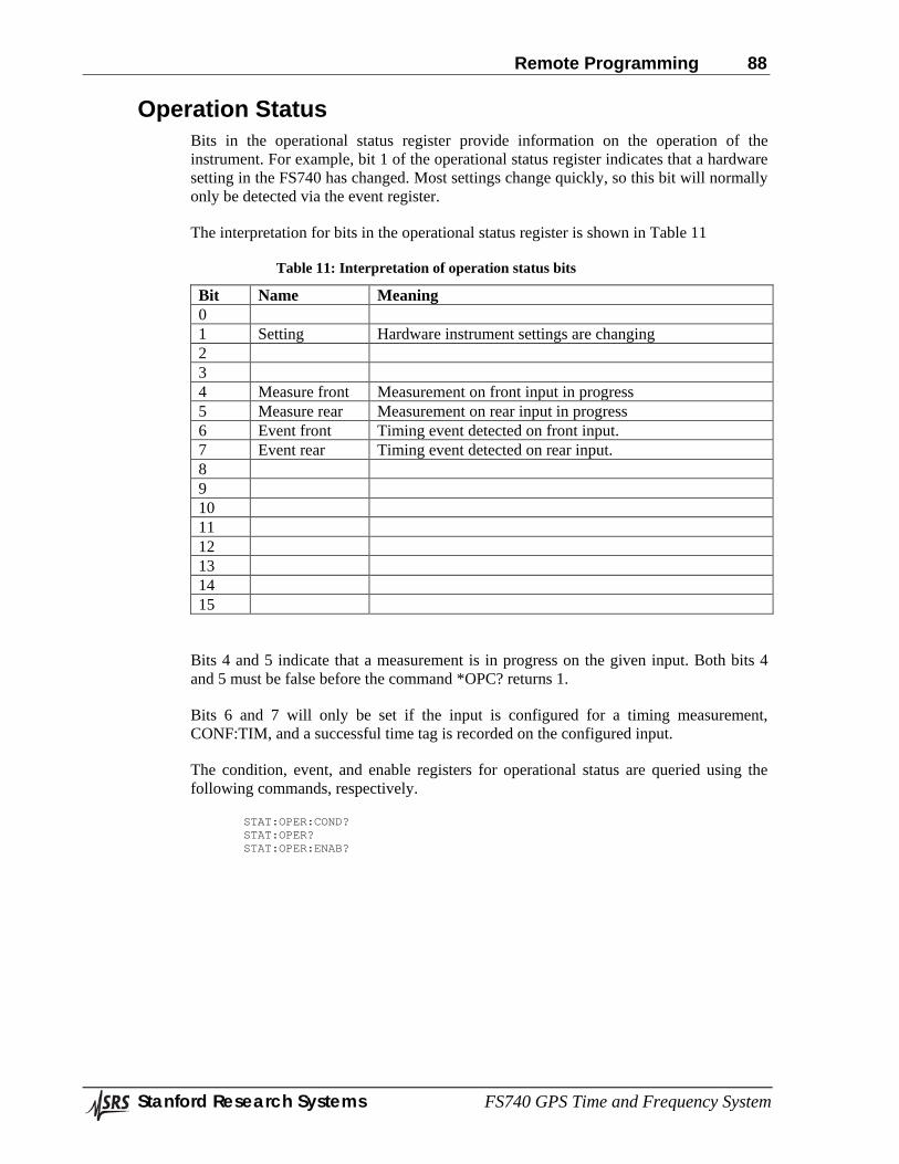
Remote Programming 88
Stanford Research Systems FS740 GPS Time and Frequency System
Operation Status Bits in the operational status register provide information on the operation of the instrument. For example, bit 1 of the operational status register indicates that a hardware setting in the FS740 has changed. Most settings change quickly, so this bit will normally only be detected via the event register.
The interpretation for bits in the operational status register is shown in Table 11
Table 11: Interpretation of operation status bits
Bit Name Meaning 0 1 Setting Hardware instrument settings are changing 2 3 4 Measure front Measurement on front input in progress 5 Measure rear Measurement on rear input in progress 6 Event front Timing event detected on front input. 7 Event rear Timing event detected on rear input. 8 9 10 11 12 13 14 15
Bits 4 and 5 indicate that a measurement is in progress on the given input. Both bits 4 and 5 must be false before the command *OPC? returns 1.
Bits 6 and 7 will only be set if the input is configured for a timing measurement, CONF:TIM, and a successful time tag is recorded on the configured input.
The condition, event, and enable registers for operational status are queried using the following commands, respectively.
STAT:OPER:COND? STAT:OPER? STAT:OPER:ENAB?
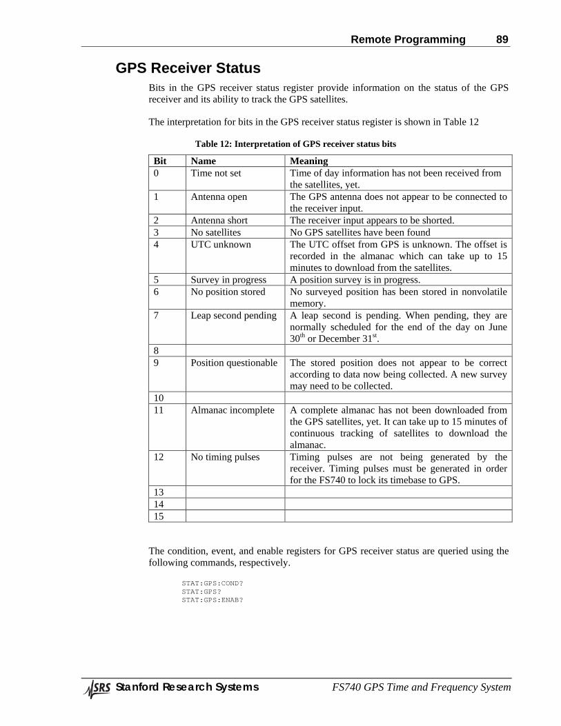
Remote Programming 89
Stanford Research Systems FS740 GPS Time and Frequency System
GPS Receiver Status Bits in the GPS receiver status register provide information on the status of the GPS receiver and its ability to track the GPS satellites.
The interpretation for bits in the GPS receiver status register is shown in Table 12
Table 12: Interpretation of GPS receiver status bits
Bit Name Meaning 0 Time not set Time of day information has not been received from
the satellites, yet. 1 Antenna open The GPS antenna does not appear to be connected to
the receiver input. 2 Antenna short The receiver input appears to be shorted. 3 No satellites No GPS satellites have been found 4 UTC unknown The UTC offset from GPS is unknown. The offset is
recorded in the almanac which can take up to 15 minutes to download from the satellites.
5 Survey in progress A position survey is in progress. 6 No position stored No surveyed position has been stored in nonvolatile
memory. 7 Leap second pending A leap second is pending. When pending, they are
normally scheduled for the end of the day on June 30th or December 31st.
8 9 Position questionable The stored position does not appear to be correct
according to data now being collected. A new survey may need to be collected.
10 11 Almanac incomplete A complete almanac has not been downloaded from
the GPS satellites, yet. It can take up to 15 minutes of continuous tracking of satellites to download the almanac.
12 No timing pulses Timing pulses are not being generated by the receiver. Timing pulses must be generated in order for the FS740 to lock its timebase to GPS.
13 14 15
The condition, event, and enable registers for GPS receiver status are queried using the following commands, respectively.
STAT:GPS:COND? STAT:GPS? STAT:GPS:ENAB?
Remote Programming 90
Stanford Research Systems FS740 GPS Time and Frequency System
Making Measurements The FS740 can make frequency and timing measurements of an external signal source. The front and rear inputs have independent circuitry enabling simultaneous measurements. All the measurement commands take an optional numerical suffix of 1 or 2. The value 1 refers to the front input. The value 2 refers to the rear input. If omitted, the front input is assumed. The SCPI language provides several ways to configure and initiate measurements, which vary in complexity and control.
Simple Measurements The MEASure commands provide the simplest method of quickly configuring a measurement and reading the result in one command.
Syntax MEASure[1|2]:FREQuency? [<expected>|MINimum|MAXimum|DEFault
[,<resolution>|MINimum|MAXimum|DEFault]] MEASure[1|2]:TIMe?
Description The first version configures a frequency measurement with default parameters. The second version configures a measurement of time. In both cases the measurement is triggered immediately and the result sent directly to the output buffer. The frequency measurement takes two optional parameters. The first is an expected frequency for the measurement. If omitted, 10 MHz is assumed. The second is the desired resolution of the measurement. If omitted, a resolution is selected such that the gate for the measurement will be 0.1 s resulting in about 11 digits of precision.
Examples To make single measurements of frequency on the front and rear inputs, use the following commands:
MEAS:FREQ? MEAS2:FREQ?
Similarly, to make single measurements of time on the front and rear inputs, use the following commands:
MEAS:TIM? MEAS2:TIM?
Configure and Read The MEASure commands configure a measurement and trigger it immediately. This does not allow the user to refine the measurement configuration. To enable finer control of the configuration, use the CONFigure and READ commands. The CONFigure commands have the same syntax and meaning as the MEASure commands discussed above, except that they are set commands rather than queries, reflecting the fact that the measurement is not triggered, and so no results will be forthcoming to read. The hardware for a given measurement is configured with default settings. The user should send additional commands to customize the configuration before the measurement is triggered. Once the configuration is complete, the user can trigger a measurement and read the result with the READ command.
Remote Programming 91
Stanford Research Systems FS740 GPS Time and Frequency System
Syntax CONFigure[1|2]:FREQ [<expected>|MINimum|MAXimum|DEFault
[,<resolution>|MINimum|MAXimum|DEFault]] CONFigure[1|2]:TIMe READ[1|2]?
Examples To configure a frequency measurement on the front input with a 1 second gate, use the following commands:
CONF:FREQ SENS:FREQ:GATE 1.0 READ? The first line configures the front input for a frequency measurement with default settings. The second line changes the gate from the default to 1.0 seconds. The last line initiates the measurement and sends it to the output buffer for reading.
The next example configures the rear input for 10 timing measurements and triggers a measurement:
CONF2:TIM SAMP2:COUN 10 READ2? The first line configures the rear input for an absolute time measurement. The second line changes the sample size of the measurement to 10. The last line initiates the measurement and sends the results to the output buffer for reading.
Initiate and Fetch The READ command discussed above triggers a measurement and sends the results immediately to the output. This is the desired result in most cases. However, sometimes it is useful to separate the initiation of the measurement and the reading of the results. This is achieved with the INITiate and FETCh commands. The initiate triggers a measurement but does not send the results to the output buffer. Instead they are sent to an internal memory buffer, which has enough space to hold the last 250,000 results. The FETCh command causes the results to be copied from the internal memory to the output buffer. A READ command is equivalent to an INITiate followed immediately by a FETCh.
Syntax INITiate[1|2][:IMMediate] FETCh[1|2]? Separating measurement initiation from the reading of the results is particularly useful when the measurement takes a long time or the sample size is large. In the former case, separating the INITiate from the FETCh enables the user to query the status registers to monitor the progress of the measurement without having to depend on long timeouts and an unresponsive unit. In the latter case when the sample size is large, it may be that the user is uninterested in the individual results and only wants to query the statistics for the measurement. In this case the FETCH command need not be sent at all. Instead, the CALC:STAT command is sent after all measurements complete.
Remote Programming 92
Stanford Research Systems FS740 GPS Time and Frequency System
Like the READ command, the FETCh command won’t complete until all samples in the measurement have completed. For large data sets this may be undesirable. In this case the user can use the DATA subsystem to query how much data is available and read only a portion of the data at a time.
Remote Programming 93
Stanford Research Systems FS740 GPS Time and Frequency System
Common IEEE-488.2 Commands *CLS Clear Status
Syntax *CLS
Description This command immediately clears all status registers as well as the SYST:ERR queue.
*ESE Standard Event Status Enable
Syntax *ESE <value> *ESE?
Description Set the Standard Event Status Enable register to <value>. The value may range from 0 to 255. Bits set in this register cause ESR (in *STB) to be set when the corresponding bit is set in the *ESR register. The query returns the current value of the enable register. Definitions for the bits in the standard event register are given on page 86.
Example *ESE 1
Enable bit 0 so that an operation complete event will set the ESR bit in the serial poll status byte.
*ESR? Standard Event Status Register
Syntax *ESR?
Description Query the Standard Event Status Register. After the query, the returned bits of the *ESR register are cleared. The bits in the ESR register have the following meaning:
Bit Meaning 0 OPC – operation complete 1 Reserved 2 QYE – query error 3 DDE – device dependent error 4 EXE – execution error 5 CME – command error 6 Reserved 7 PON – power-on
See page 86 for more detailed information on the event status register.
Example *ESR?
A return of ‘176’ would indicate that PON, CME, and EXE are set.
Remote Programming 94
Stanford Research Systems FS740 GPS Time and Frequency System
*IDN? Identification String
Syntax *IDN?
Description Query the instrument identification string.
Example *IDN?
Returns a string similar to ‘Stanford Research Systems,FS740,s/n004025,ver2.26.11’
*OPC Operation Complete
Syntax *OPC *OPC?
Description The set form sets the OPC flag in the *ESR register when all prior commands have completed. The query form returns ‘1’ when all prior commands have completed, but does not affect the *ESR register.
*OPT? Options
Syntax *OPT?
Description The query returns a comma separated list of the four possible installed options in the following order: installed timebase, top rear panel board, middle rear panel board, and bottom rear panel board. They may take on the following values:
Type Option Value Timebase TCXO 0
OCXO 1 Rb 2
Board 10 MHz distribution A Sine/Aux output distribution B Pulse output distribution C Not installed D
Example *OPT?
The query returns the current installed options. A return of “2,A,B,C” would indicate that a Rb timebase is installed; a 10 MHz distribution board is installed in the top slot; a Sine/Aux distribution board is installed in the middle slot; a pulse distribution board is installed in the bottom slot.
Remote Programming 95
Stanford Research Systems FS740 GPS Time and Frequency System
*PSC Power-on Status Clear
Syntax *PSC <value> *PSC?
Description Set the Power-on Status Clear flag to <value>. The Power-on Status Clear flag is stored in nonvolatile memory in the unit, and thus, maintains its value through power-cycle events.
If the value of the flag is 0, then the Service Request Enable and Standard Event Status Enable Registers (*SRE, *ESE) are stored in non-volatile memory, and retain their values through power-cycle events. If the value of the flag is 1, then these two registers are cleared upon power-cycle.
Example Use the following commands to set power on status clear to 1 and then query the setting.
*PSC 1 *PSC?
*RCL Recall Instrument Settings
Syntax *RCL <location>
Description Recall instrument settings from <location>. The <location> may range from 0 to 9. Locations 1 to 9 are for arbitrary use. Location 0 is reserved for the recall of default instrument settings.
Example *RCL 3
Recall instruments settings from location 3.
*RST Reset Instrument
Syntax *RST
Description Reset the instrument to default settings. This is equivalent to *RCL 0. See Factory Default Settings on page 71 for a list of default settings.
*SAV Save Instrument Settings
Syntax *SAV <location>
Description Save instrument settings to <location>. The <location> may range from 0 to 9. However, location 0 is reserved for current instrument settings. It will be overwritten after each front panel key press.
Remote Programming 96
Stanford Research Systems FS740 GPS Time and Frequency System
Example *SAV 3
Save current instrument settings to location 3.
*SRE Service Request Enable
Syntax *SRE <value> *SRE?
Description Set the Service Request Enable register to <value>. Bits set in this register cause the FS740 to generate a service request when the corresponding bit is set in the serial poll status register, *STB.
Example *SRE 16
Set bit 4 of the enable register. This will generate a service request when the FS740 has bytes in its output buffer ready to be read. Definitions for the bits in the serial poll status byte are given on page 84.
*STB? Status Byte
Syntax *STB?
Description Query the standard IEEE 488.2 serial poll status byte. The bits in the STB register have the following meaning:
Bit Meaning 0 Reserved 1 GPS status summary bit 2 Error queue is not empty 3 Questionable status summary bit 4 Message available, MAV. 5 ESR status summary bit 6 MSS – master summary bit 7 Operational status summary bit
See page 84 for more detailed information on the serial poll status byte.
Example *STB?
A return of ‘114’ would indicate that GPS, MAV, ESR, and MSS are set. GPS indicates that an enabled bit in STAT:GPS is set. MAV indicates that a message is available in the output queue. ESR indicates that an enabled bit in the *ESR is set. MSS reflects the fact that at least one of the summary enable bits is set and the instrument is requesting service.
*WAI Wait for Command Execution
Remote Programming 97
Stanford Research Systems FS740 GPS Time and Frequency System
Syntax *WAI
Description The instrument will not process further commands until all prior commands including this one have completed.
Example *WAI
Wait for all prior commands to execute before continuing.
Remote Programming 98
Stanford Research Systems FS740 GPS Time and Frequency System
Measurement Commands Measurement commands can apply to either the front or rear input. The user selects the input by optionally appending a 1 or 2 to the root keyword of the command. When the suffix is 1 or omitted, the front input is selected. When the suffix is 2, the rear input is selected. For example, the following commands all apply to the front input:
MEAS:FREQ? CONF1:TIM READ1? CONF:FREQ INIT1 FETC?
Notice that the suffix is optional when referring to the front input. Modify the commands as follows to make them apply to the rear input:
MEAS2:FREQ? CONF2:TIM READ2? CONF2:FREQ INIT2 FETC2?
Here, the suffix is required.
MEASure:FREQuency? Measure Frequency
Syntax MEASure[1|2]:FREQuency? [<expected>|MINimum|MAXimum|DEFault
[,<resolution>|MINimum|MAXimum|DEFault]]
Description Configures hardware for a frequency measurement and immediately triggers a measurement and sends the result to the output buffer. The first parameter is optional and informs the instrument of the expected frequency of the signal. The second parameter is also optional. It sets the requested resolution of the measurement. Neither parameter is used directly by the FS740. Instead the ratio of the resolution to the expected frequency is used to set the gate time for the measurement. If the parameters are omitted, a gate time of 0.1 second is used which corresponds to approximately 11 digits of precision. Measurements are returned as floating point values in units of Hz. If a measurement times out NAN is returned.
Example MEAS:FREQ?
Configure a frequency measurement on the front panel input, using the default 0.1 s gate. Trigger the measurement immediately and send the result to the output buffer for reading.
MEASure:TIMe? Measure Time
Syntax MEASure[1|2]:TIMe?
Description Configures hardware for a measurement of time and immediately triggers a measurement and sends the result to the output buffer. A single result consists of 11 comma separated integer values in the
Remote Programming 99
Stanford Research Systems FS740 GPS Time and Frequency System
following order: timing metric, year, month, day, hour, minute, seconds, milliseconds, microseconds, nanoseconds, picoseconds. The timing metric is a copy of the questionable status register at the time of the measurement.
Example MEAS2:TIM?
Configure a measurement of time on the rear panel input. Trigger the measurement immediately and send the result to the output buffer for reading.
CONFigure? Configure
Syntax CONFigure[1|2]?
Description Query the current measurement configuration. The command returns a quoted string with the measurement type and parameters used to configure the measurement.
Example CONF:FREQ CONF?
Configure a measurement of frequency on the front panel input. The query will return: FREQ 1.0e+07,1.0e-04.
CONFigure:FREQuency Configure Frequency
Syntax CONFigure[1|2]:FREQuency [<expected>|MINimum|MAXimum|DEFault
[,<resolution>|MINimum|MAXimum|DEFault]]
Description Configure the hardware for a frequency measurement. This is identical to the MEASure command except that the measurement isn’t triggered and sent to the output buffer. Like the MEASure command, the first parameter is optional and informs the instrument of the expected frequency of the signal. The second parameter is also optional. It sets the requested resolution of the measurement. Neither parameter is used directly by the FS740. Instead the ratio of the resolution to the expected frequency is used to set the gate time for the measurement. If the parameters are omitted, a gate time of 0.1 second is used which corresponds to approximately 11 digits of precision. Measurement results are returned with a READ command as floating point values in units of Hz. If a measurement times out, NAN is returned.
Example CONF:FREQ SENS:FREQ:GATE 1.0 READ?
Configure a frequency measurement on the front panel input, using the default 0.1 s gate. Then change the gate to 1.0 s. Finally trigger a measurement and read the result.
CONFigure:TIMe Configure Time
Remote Programming 100
Stanford Research Systems FS740 GPS Time and Frequency System
Syntax CONFigure[1|2]:TIMe
Description Configures hardware for a measurement of time and immediately triggers a measurement and sends the result to the output buffer. Results are returned with a READ command. A single result consists of 11 comma separated integer values in the following order: timing metric, year, month, day, hour, minute, seconds, milliseconds, microseconds, nanoseconds, picoseconds. The timing metric is a copy of the questionable status register at the time of the measurement.
Example CONF2:TIM SAMP2:COUN 10 READ2?
Configure a measurement of time on the rear panel input. Change the sample count from 1 to 10. Finally trigger the measurement and read the results.
READ? Read Results
Syntax READ[1|2]?
Description Trigger a measurement using the current configuration and read the result. See commands MEASure:FREQuency and MEASure:TIMe for details on the format of results returned. When the sample size is greater than one, results are separated from each other by commas ( , ).
Example CONF:FREQ SENS:FREQ:GATE 1.0 READ?
Configure a measurement of frequency on the front panel input. Then change the gate time for the measurement to 1.0 s. Finally trigger the measurement and read the result.
INITiate Initiate Measurement
Syntax INITiate[1|2][:IMMediate]
Description Trigger a measurement using the current configuration but leave the results in internal memory. The internal memory has enough space to store the last 250,000 measurements. The user should send the FETCh command to retrieve the results from internal memory. Alternatively, the user may use commands in the DATA subsystem to read only a portion of the results.
Example CONF:FREQ SAMP:COUN 1000 INIT FETC?
Remote Programming 101
Stanford Research Systems FS740 GPS Time and Frequency System
Configure a measurement of frequency on the front panel input using default settings. Then change the sample count from 1 to 1000. Then initiate a measurement. Finally read out the results.
FETCh? Fetch Results
Syntax FETCh[1|2]?
Description Copy results stored in the internal buffer to the output buffer for reading. Like the READ command, this command will not complete until all measurements have completed. See commands MEASure:FREQuency and MEASure:TIMe for details on the format of results returned. When the sample size is greater than one, results are separated from each other by commas ( , ).
Example CONF:FREQ SAMP:COUN 1000 INIT FETC?
Configure a measurement of frequency on the front panel input using default settings. Then change the sample count from 1 to 1000. Next initiate a measurement. Finally read out the results, which should contain 1000 frequency measurements.
ABORt Abort Measurement
Syntax ABORt[1|2]
Description Abort any measurement in progress and discard any results produced by it.
Example ABOR
Abort any measurement initiated on the front input.
STOP Stop Measurement
Syntax STOP[1|2]
Description Stop any measurement in progress, but do not discard any results produced by it.
Example CONF:FREQ SAMP:COUN 1000 INIT STOP FETC?
Remote Programming 102
Stanford Research Systems FS740 GPS Time and Frequency System
Configure the front input for a frequency measurement. Change the sample count to 1000. Initiate the measurement. Stop the measurement but do not discard any results already produced. Fetch those results
Calculate Subsystem Commands in the Calculate Subsystem can apply to either the front or rear input. The user selects the input by optionally appending a 1 or 2 to the CALCulate keyword. When the suffix is 1 or omitted, the front input is selected. When the suffix is 2, the rear input is selected.
CALCulate:FILTer Calculation Filter
Syntax CALCulate[1|2]:FILTer NONE|FAST CALCulate[1|2]:FILTer?
Description The first definition changes input filter for frequency measurements. The second definition queries the current input filter. There are two filter options: NONE and FAST. If NONE is selected, then just two time tags are used to generate a frequency measurement, one at the beginning of the gate interval and one at the end. When the FAST filter is selected, up to 625 time tags are averaged together at the beginning of the gate interval to produce an average starting time tag. Another 625 time tags are averaged together at the end of the gate interval to produce an average ending time tag. These two averaged time tags are used to compute a frequency measurement. The benefit of this filter is that it is effective in removing broadband noise inherent in the measurement. Noise can be reduced by more than a factor of 10 with the use of this filter. The default filter is FAST and it is the recommended setting for most measurements. The following example shows how to turn off the filter, if desired.
Example CONF:FREQ CALC:FILT NONE READ?
Configure front input for a frequency measurement. Turn off the FAST filter. Trigger a measurement and read the results.
CALCulate:REFerence Calculation Reference Frequency
Syntax CALCulate[1|2]:REFerence [<frequency>|MINimum|MAXimum|DEFault] CALCulate[1|2]:REFerence?
Description For each frequency measurement, the reference frequency is subtracted from the measured frequency to produce the final result. This enables one to monitor the deviation of the frequency from a specified target value rather than the absolute frequency itself. The first definition sets the reference frequency to <frequency>. If <frequency> is omitted, it is set to the value of the most recent measurement. The second definition queries the current reference frequency. The default reference frequency is 0 Hz.
Remote Programming 103
Stanford Research Systems FS740 GPS Time and Frequency System
Example CONF:FREQ CALC:REF 10MHz READ?
Configure front input for a frequency measurement. Set the reference frequency to 10 MHz. Measure the deviation of the input from 10MHz.
CALCulate:STABility Calculate Frequency Stability
Syntax CALCulate[1|2]:STABility[:ALL]?
Description This command computes the frequency stability, or Allan deviation, of all frequency measurements for time intervals from 10 ms to 50 million seconds in a 1, 2, 5 sequence and returns them as a comma delimited list of relative Allan deviations. The first is the computed stability for a 10 ms interval. The second is for a 20 ms interval. The third is for a 50 ms interval and so forth. Each succeeding stability measurement is for an interval that increases in a 1, 2, 5 sequence with the 30th value corresponding to an interval of 50 million seconds. If the data set is not large enough to compute a valid stability for a given interval, zero is returned for that entry. Note that the FS740 is computing averaged time tags every 10 ms with no dead time, regardless of the configured gate. This enables the FS740 to compute the frequency stability for all time intervals, not just the configured gate interval. Furthermore, the user need not wait for the measurement to complete before sending this command. It will return the computed stability of all measurements completed at the time of the query.
Example CONF:FREQ SENS:FREQ:GATE 1.0 SAMP:COUN 1000000 INIT … CALC:STAB?
Configure front input for a frequency measurement. Set the gate to 1.0 s and the sample size to 1 million. Start the measurement. Wait. Then query the computed frequency stability of the measurements. Note that one need not wait for the measurement to complete. The FS740 will return the computed stability for all measurements completed so far.
CALCulate:STATistics Calculate Measurement Statistics
Syntax CALCulate[1|2]:STATistics[:ALL]?
Description This command computes some basic statistics of the current measurement and returns the following values in a comma separated list: the mean, the Allan deviation, the minimum, the maximum, and the number of measurements made. The statistical values returned are in Hz, including the Allan deviation. To get a relative stability, divide the returned Allan deviation by the mean. The Allan deviation returned is only for the configured gate interval, and is computed only from the measurements stored in internal memory. This is in contrast to the results returned by the CALC:STAB command which incorporates many more time tags not included in the frequency measurements stored in internal memory.
Remote Programming 104
Stanford Research Systems FS740 GPS Time and Frequency System
Example CONF:FREQ SENS:FREQ:GATE 1.0 SAMP:COUN 1000 INIT … CALC:STAT?
Configure front input for a frequency measurement. Set the gate to 1.0s and the sample size to 1000. Start the measurement. Wait. Then query the statistics for the measurements. Note that one need not wait for the measurement to complete. The FS740 will return the computed statistics for all measurements completed so far.
Data Subsystem FS740 has enough internal memory to store 250,000 results for both the front and rear input. The Data Subsystem enables the user to query and process these results. Commands in the Data Subsystem can apply to either the front or rear input. The user selects the input by optionally appending a 1 or 2 to the DATA keyword. When the suffix is 1 or omitted, the front input is selected. When the suffix is 2, the rear input is selected.
DATA:COUNt? Data Count
Syntax DATA[1|2]:COUNt?
Description This command returns the total number of measurements completed so far.
Example CONF:FREQ SAMP:COUN 100 INIT … DATA:COUN?
Configure front input for a frequency measurement. Set the sample size to 100. Start the measurement. Wait. Then query the number of measurements completed for the front input. When all measurements are complete, the returned value should agree with the configured sample count.
DATA:POINts? Data Points
Syntax DATA[1|2]:POINts?
Description This command returns the total number of measurements stored in internal memory. This number may differ from the DATA:COUNT if some data has been removed with a DATA:REM command or if the total number of measurements causes the internal memory to overflow. In the latter case, only the most recent measurements are kept. The internal memory has space to store up to 250,000 measurements.
Example CONF2:FREQ
Remote Programming 105
Stanford Research Systems FS740 GPS Time and Frequency System
SAMP2:COUN 100 INIT2 … DATA2:POIN?
Configure rear input for a frequency measurement. Set the sample size to 100. Start the measurement. Wait. Then query the number of measurements stored in internal memory for the rear input. These values may be read immediately using a DATA:READ or DATA:REM command.
DATA:READ? Data Read
Syntax DATA[1|2]:READ? [<index>][,<count>]
Description This command returns <count> measurements stored in internal memory, starting with the one located at <index>. The first measurement in memory has an <index> of 0. The second has an <index> of 1, and so on. The user should send the DATA:POIN command to determine how many measurements are stored in memory. If omitted, <index> is assumed to be 0. If omitted, <count> is assumed to be 1. If <index> or <count> is out of range, error −222, “Data out of range,” is generated and no data returned. See commands MEASure:FREQuency and MEASure:TIMe for details on the format of results returned. When the sample size is greater than one, results are separated from each other by commas ( , ).
Example CONF2:FREQ SAMP2:COUN 100 INIT2 … DATA2:POIN? DATA2:READ? 10, 5
Configure rear input for a frequency measurement. Set the sample size to 100. Start the measurement. Wait. Then query the number of measurements stored in internal memory for the rear input. Retrieve 5 measurements starting with the measurement at index 10.
DATA:REMove? Data Remove
Syntax DATA[1|2]:REMove? <count>
Description This command returns the first <count> measurements stored in internal memory and removes them from memory. If the requested <count> exceeds the amount of data available, error −222, “Data out of range,” is generated and no data is returned. This command is useful if the configured sample count is larger than can be stored in internal memory. It enables the user to retrieve measurements as they become available to free up space in internal memory so that no measurement results are lost. See commands MEASure:FREQuency and MEASure:TIMe for details on the format of results returned. When the sample size is greater than one, results are separated from each other by commas ( , ).
Example CONF:FREQ SAMP:COUN 1000000 INIT
Remote Programming 106
Stanford Research Systems FS740 GPS Time and Frequency System
… DATA:POIN? DATA:REM? 100
Configure front input for a frequency measurement. Set the sample size to 1 million. Start the measurement. Wait. Then query the number of measurements stored in internal memory for the front input. Retrieve the first 100 measurements and remove them from memory.
GPS Subsystem Commands in the GPS Subsystem enable configuration of the GPS receiver and report on its operation.
GPS:CONFig:CONStellation GPS Configure Constellation
Syntax GPS:CONFig:CONStellation <constellation mask> GPS:CONFig:CONStellation?
Description The first definition enables the user to set the combination of satellites tracked. The second definition queries the current combination of satellites being tracked. The constellation mask is a single number from 1 to 15 whose binary bits identify the combination of satellites that should be tracked as identified in Table 13. The default constellation mask is 3, which has bits 0 and 1 set, meaning GPS and GLONASS will be tracked. The user must execute the command GPS:CONF:SAVE to save the current values to nonvolatile memory. Note that not all combinations are supported. If an unsupported combination is requested, the command will be ignored without reporting an error.
Table 13: Constellation bit definitions
Bit Constellation 0 GPS 1 GLONASS 2 BEIDOU 3 GALILEO
Example GPS:CONF:CONS 3
Configure the GNSS receiver to track GPS and GLONASS.
GPS:CONFig:MODe GPS Configure Mode
Syntax GPS:CONFig:MODe <anti-jamming>, <elevation mask>, <signal mask> GPS:CONFig:MODe?
Description The first definition enables the user to set anti-jamming mode, the elevation mask and the signal mask. The second definition queries the current values for these parameters. <Anti-jamming> is a Boolean value which enables or disables anti-jamming in the receiver. The factory default is enabled. <Elevation mask> is the elevation angle in radians, below which satellites are ignored in over determined clock mode. It can range from 0 to π/2. <Signal mask> is the minimum signal level in
Remote Programming 107
Stanford Research Systems FS740 GPS Time and Frequency System
dbHz, below which satellites are ignored in over determined clock mode. It can range from 0 to 55 dBHz. The default value for both masks is 0. The user must execute the command GPS:CONF:SAVE to save the current values to nonvolatile memory.
Example GPS:CONF:MODE 1,0.2618,10
Enable anti-jamming. Set elevation mask to 15 degrees = 0.2618 radians. Set the minimum signal level to 10 dbHz. These limits only apply in over determined clock mode.
GPS:CONFig:SAVe GPS Configure Save
Syntax GPS:CONFig:SAVe
Description The user uses commands in the GPS:CONFIG subsystem to configure the operation of the receiver. The configuration is lost, however, if the power is cycled unless this command is executed. It saves the current GPS receiver configuration to nonvolatile memory, so that it may be automatically recalled when the power is cycled.
Example GPS:CONF:SAV
Save the current GPS receiver configuration to nonvolatile memory.
GPS:CONFig:SURVey:Mode GPS Configure Survey Mode
Syntax GPS:CONFig:SURVey[:MODe] [DISabled|REDo|REMember] GPS:CONFig:SURVey[:MODe]?
Description The first definition sets the GPS survey mode to the given configuration. If mode is omitted, the default mode is REDo. The second definition queries the current GPS survey mode. When DISabled is selected no survey is carried out. This mode is appropriate in mobile environments. REDo causes the survey to be repeated each time the instrument is power cycled. REMember causes the results of the survey to be saved in nonvolatile memory. When the instrument is power cycled, the surveyed position is recalled from memory and the survey is not repeated. The user must execute the command GPS:CONF:SAVE to save the current value to nonvolatile memory.
Example GPS:CONF:SURV REM
Configure the GPS receiver to do a survey at startup the first time, but to remember the results of the first survey from then on rather than repeating the survey.
GPS:CONFig:SURVey:FIXes GPS Configure Survey Fixes
Syntax GPS:CONFig:SURVey:FIXes [<fixes>] GPS:CONFig:SURVey:FIXes?
Remote Programming 108
Stanford Research Systems FS740 GPS Time and Frequency System
Description The first definition sets the number of position fixes in the survey. If <fixes> is omitted, the default number is 2000. The second definition queries the current number of position fixes in the position survey. This is the number of position fixes that get averaged together to define the GPS antennas location. Once the position is well known, the receiver can be put into over determined clock mode and the receiver can provide improved timing by dedicating the signal from all satellites to timing. The user must execute the command GPS:CONF:SAVE to save the current value to nonvolatile memory.
Example GPS:CONF:SURV:FIX 3000
Configure the GPS receiver to include 3000 position fixes in the position survey.
GPS:CONFig:ALIGnment GPS Configure Timing Alignment
Syntax GPS:CONFig[:TIMing]:ALIGnment [GPS|UTC] GPS:CONFig[:TIMing]:ALIGnment?
Description The first definition sets the GPS 1pps alignment. If alignment is omitted, the default alignment is UTC. The second definition queries the current GPS 1pps alignment. When GPS is selected, all timing is aligned to GPS. When UTC is selected, all timing is aligned to UTC. The user must execute the command GPS:CONF:SAVE to save the current value to nonvolatile memory.
Example GPS:CONF:ALIG UTC
Alignment of the GPS 1pps is to UTC.
GPS:CONFig:QUALity GPS Configure Timing Quality
Syntax GPS:CONFig[:TIMing]:QUALity [1SAT|3SAT] GPS:CONFig[:TIMing]:QUALity?
Description The first definition sets the minimum number of satellites the receiver must track before outputting a hardware 1pps pulse. If omitted, the default quality is 3 satellites. The second definition queries the current timing quality. Timing quality generally increases as the number of satellites increases. However, the user must also consider reliability and holdover performance. Degraded performance may be preferred over no timing whatsoever. The user must execute the command GPS:CONF:SAVE to save the current value to nonvolatile memory.
Example GPS:CONF:QUAL 3SAT
Require the GPS receiver to track 3 satellites before outputting a hardware 1pps pulse for the timebase to track.
GPS:CONFig:ADELay GPS Configure Timing Antenna Delay
Remote Programming 109
Stanford Research Systems FS740 GPS Time and Frequency System
Syntax GPS:CONFig[:TIMing]:ADELay <delay> GPS:CONFig[:TIMing]:ADELay?
Description The first definition sets the antenna delay to <delay> in seconds. The second definition queries the current antenna delay in seconds. The <delay> may range from −0.1 s to +0.1 s. Note that the user should enter a negative number here to compensate for the length of their antenna cable. It affects the timing of all inputs and outputs. The user must execute the command GPS:CONF:SAVE to save the current value to nonvolatile memory.
Example GPS:CONF:ADEL -100ns
Set delay to −100 ns. This advances the timing generated by the GPS receiver by 100 ns.
GPS:POSition? GPS Position
Syntax GPS:POSition?
Description Query the GPS position. This routine returns the surveyed average position of the receiver in latitude, longitude, and altitude. Latitude is specified in radians, with positive values indicating north, and negative values indicating south. Longitude is specified in radians, with positive values indicating east, and negative values indicating west. Altitude is specified in meters above average sea levels.
Example GPS:POS?
Query the current surveyed position of the GPS receiver.
GPS:POSition:HOLD:STATe? GPS Position Hold State
Syntax GPS:POSition:HOLD:STATe?
Description Query whether the GPS receiver is in position hold mode where all satellites are being used for maximum timing performance. The query will return 1 if the receiver is in position hold mode, otherwise 0. The receiver typically enters position hold mode once the position survey is complete.
Example GPS:POS:HOLD:STAT?
Query whether the GPS receiver has entered position hold mode.
GPS:POSition:SURVey:DELete GPS Position Survey Delete
Syntax GPS:POSition:SURVey:DELete
Remote Programming 110
Stanford Research Systems FS740 GPS Time and Frequency System
Description Delete the surveyed position stored in nonvolatile memory, if any.
Example GPS:POS:SURV:DEL
Delete the current stored position in nonvolatile memory.
GPS:POSition:SURVey:PROGress? GPS Position Survey Progress
Syntax GPS:POSition:SURVey:PROGress?
Description Query how much of the position survey has completed. The FS740 will return an integer between 0 and 100 %.
Example GPS:POS:SURV:PROG?
Query the progress of the position survey by the GPS receiver.
GPS:POSition:SURVey:SAVe GPS Position Survey Save
Syntax GPS:POSition:SURVey:SAVe
Description Save the current position in nonvolatile memory. The receiver will subsequently use it to enter position hold mode where all satellites are used for maximum timing performance.
Example GPS:POS:SURV:SAV
Save the current position in nonvolatile memory.
GPS:POSition:SURVey:STARt GPS Position Survey Start
Syntax GPS:POSition:SURVey:STARt
Description Restart the GPS receiver’s position survey. Note that previously saved results are not deleted by this command.
Example GPS:POS:SURV:STAR
Restart the GPS receiver’s position survey.
GPS:POSition:SURVey:STATe? GPS Position Survey State
Remote Programming 111
Stanford Research Systems FS740 GPS Time and Frequency System
Syntax GPS:POSition:SURVey:STATe?
Description Query whether a position survey is in progress or not. The query returns 1 if the survey is in progress, otherwise 0.
Example GPS:POS:SURV:STAT
Query whether a position survey is in progress.
GPS:SATellite:TRACking? GPS Satellite Tracking
Syntax GPS:SATellite:TRACking?
Description Query which GPS satellites are being tracked by the receiver. The query returns the number of satellites being tracked, followed by the IDs of the satellites as a comma ( , ) separated list.
Example GPS:SAT:TRAC?
Query the number and IDs of the satellites being tracked by the receiver.
GPS:SATellite:TRACking:STATus? GPS Satellite Tracking Status
Syntax GPS:SATellite:TRACking:STATus?
Description The receiver has 20 channels for tracking satellites. This command returns the information shown in Table 14 for each channel, successively:
Table 14: Satellite tracking information
Index Parameter 0 Satellite ID number 1 Acquired 2 Ephemeris 3 Is old 4 Signal level in dbHz 5 Elevation in degrees 6 Azimuth in degrees 7 Space vehicle type
If a channel is not tracking a satellite, it will return zero for all parameters. In all, 20 × 8 = 160 parameters are returned as a comma ( , ) separated list.
Example GPS:SAT:TRAC:STAT?
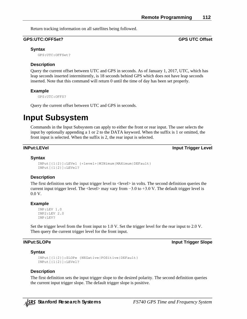
Remote Programming 112
Stanford Research Systems FS740 GPS Time and Frequency System
Return tracking information on all satellites being followed.
GPS:UTC:OFFSet? GPS UTC Offset
Syntax GPS:UTC:OFFSet?
Description Query the current offset between UTC and GPS in seconds. As of January 1, 2017, UTC, which has leap seconds inserted intermittently, is 18 seconds behind GPS which does not have leap seconds inserted. Note that this command will return 0 until the time of day has been set properly.
Example GPS:UTC:OFFS?
Query the current offset between UTC and GPS in seconds.
Input Subsystem Commands in the Input Subsystem can apply to either the front or rear input. The user selects the input by optionally appending a 1 or 2 to the DATA keyword. When the suffix is 1 or omitted, the front input is selected. When the suffix is 2, the rear input is selected.
INPut:LEVel Input Trigger Level
Syntax INPut[1|2]:LEVel <level>|MINimum|MAXimum|DEFault INPut[1|2]:LEVel?
Description The first definition sets the input trigger level to <level> in volts. The second definition queries the current input trigger level. The <level> may vary from −3.0 to +3.0 V. The default trigger level is 0.0 V.
Example INP:LEV 1.0 INP2:LEV 2.0 INP:LEV?
Set the trigger level from the front input to 1.0 V. Set the trigger level for the rear input to 2.0 V. Then query the current trigger level for the front input.
INPut:SLOPe Input Trigger Slope
Syntax INPut[1|2]:SLOPe NEGative|POSitive|DEFault INPut[1|2]:LEVel?
Description The first definition sets the input trigger slope to the desired polarity. The second definition queries the current input trigger slope. The default trigger slope is positive.
Remote Programming 113
Stanford Research Systems FS740 GPS Time and Frequency System
Example INP:SLOP POS INP2:SLOP NEG INP:SLOP?
Set the front input trigger slope to positive. Set the rear input trigger slope to negative. Then query the current trigger slope for the front input.
Route Subsystem Commands in the Route Subsystem enable the users to configure the routing of signals to the Sine/Aux option boards. The rear panel of the FS740 accepts the installation of 1 to 3 option boards for the distribution of 10 MHz, the Sine/Aux outputs, or the Pulse outputs. The Sine/Aux option boards can distribute either the Sine outputs or the Aux outputs. Commands in the Route Subsystem enable the user to select which signal to distribute on these boards.
ROUTe:OPTion Route Option
Syntax ROUTe:OPTion[1|2|3] [SINe|AUX] ROUTe:OPTion[1|2|3]?
Description The first definition sets the desired distribution signal for the given option. The second definition returns the current routing for the given option. These values only have significance if a Sine/Aux option is actually installed in the appropriate slot. This value is not affected by a *RST and is stored in nonvolatile memory so that it is automatically recalled when the instrument is power cycled.
Example ROUT:OPT1 AUX ROUT:OPT2 SIN
Route the Aux signal to be distributed on option 1. Route the Sine signal to be distributed on option 2.
Sample Subsystem Commands in the Sample Subsystem can apply to either the front or rear input. The user selects the input by optionally appending a 1 or 2 to the SAMPle keyword. When the suffix is 1 or omitted, the front input is selected. When the suffix is 2, the rear input is selected.
SAMPle:COUNt Sample Count
Syntax SAMPle[1|2]:COUNt <count>|MINimum|MAXimum|DEFault SAMPle[1|2]:COUNt?
Description The first definition changes the number of samples for a configured measurement to <count>. The second definition queries the current sample count. The <count> may vary from 1 to 1,000,000,000. The default count is 1.
Remote Programming 114
Stanford Research Systems FS740 GPS Time and Frequency System
Example CONF:FREQ SAMP:COUN 1000 READ?
Configure front input for a frequency measurement. Change the sample count to 1000. Trigger a measurement and read the results. The following command queries the current sample count for the rear input.
SAMP2:COUN?
Sense Subsystem The Sense Subsystem enables the user to refine the selected measurement configuration. Commands in the Sense Subsystem can apply to either the front or rear input. The user selects the input by optionally appending a 1 or 2 to the SENSe keyword. When the suffix is 1 or omitted, the front input is selected. When the suffix is 2, the rear input is selected.
SENSe:FREQuency:GATE Frequency Gate Interval
Syntax SENSe[1|2]:FREQuency:GATE[:TIME] <duration>|MINimum|MAXimum|DEFault SENSe[1|2]:FREQuency:GATE[:TIME]? [MINimum|MAXimum|DEFault]
Description The first definition sets gate interval for frequency measurements to <duration> in seconds. The gate interval may range from 10 ms to 1000 s. The default is 0.1 s. The user may alternatively use the keywords to set the duration to the desired limit. The second definition queries the current gate interval when the optional keywords are omitted. Otherwise, the specified limit is returned.
Example CONF:FREQ SENS:FREQ:GATE 1.0 CONF2:FREQ SENS2:FREQ:GATE MIN SENS2:FREQ:GATE? READ? READ2?
Configure the front input for frequency measurements. Set the gate interval to 1.0 for the front input. Configure the rear input for frequency measurements. Set the gate interval to the minimum allowed value for the rear input. Then query the current gate interval for the rear input. Trigger a frequency measurement and read the result for the front input. Trigger a frequency measurement and read the result for the rear input.
SENSe:FREQuency:TIMeout Frequency Timeout
Syntax SENSe[1|2]:FREQuency:TIMeout <timeout>|MINimum|MAXimum|DEFault|INFinity SENSe[1|2]:FREQuency:TIMeout? [MINimum|MAXimum|DEFault]
Description The first definition sets time out period for frequency measurements to <timeout> in seconds. The timeout may range from 10 ms to 2000 s. The default is 1.0 s. The user may alternatively use the
Remote Programming 115
Stanford Research Systems FS740 GPS Time and Frequency System
keywords to set the duration to the desired limit. The second definition queries the current frequency time out period when the optional keywords are omitted. Otherwise, the specified limit is returned.
Note that measurement time outs are tied to the arrival of triggers on the input. A measurement will time out if the arrival between two successive edges on the input exceeds the time out interval. With this scheme, one need not worry about configuring time outs for most signals. For the default time out of 1 s, a time out will not occur if the signal frequency is greater than 1 Hz, regardless of the configured gate interval. Total measurement time, however, will closely follow the gate interval in most cases.
When a time out does occur during a frequency measurement, the FS740 returns NAN for that sample, and moves onto the next sample in the set of measurements. NAN is defined by SCPI to be 9.91e37.
Example CONF:FREQ SENS:FREQ:GATE 20.0 SENS:FREQ:TIM 10.0 READ?
Configure the front input for frequency measurements. Set the gate interval to 20 s for the front input. Set the measurement time out to 10 s Trigger a frequency measurement and read the result for the rear input. Changing the time out to 10 s is appropriate for signals whose frequency is between 0.1 and 1.0 Hz.
SENSe:TIMe:BMODe Time Buffer Mode
Syntax SENSe[1|2]:TIMe:BMODe KFIRst|KLASt SENSe[1|2]:TIMe:BMODe?
Description The first definition sets buffer mode for time measurements. The second definition queries the current buffer mode for time measurements. The internal buffer has space to hold 250,000 time measurements. This command controls the behavior of the FS740 when more than 250,000 measurements are made. If KFIRst (Keep First) is specified then older measurements are preserved and new measurements are dropped. If KLASt (Keep Last) is specified then older measurements are dropped and newer measurements are preserved. The default value is KLASt.
Example CONF:TIM SENS:TIM:BMOD KFIR SAMP:COUN 1000000 INIT
Configure the front input for time measurements. Set the buffer mode to keep first. Set the sample size to 1 million. Start the measurement. After 250,000 time tags are recorded, newer time tags will be dropped unless space is created by removing measurements with the DATA:REMove command.
Source Subsystem The Source Subsystem enables users to configure the frequency and amplitude of the FS740’s various source outputs. Commands can apply to one of three possible outputs: the sine output, the aux output, or the pulse output. The user selects the output by optionally appending a 1, 2 or 3 to the SOURCe keyword. When the suffix is 1 or omitted, the sine output is selected. When the suffix is 2,
Remote Programming 116
Stanford Research Systems FS740 GPS Time and Frequency System
the aux output is selected. When the suffix is 3 the pulse output is selected. Note that some commands may not apply to all outputs. In those cases the allowed suffixes are restricted to those outputs for which the command is supported.
SOURce:FREQuency Source Frequency
Syntax SOURce[1|2|3]:FREQuency[:CW|:FIXed] <freq>|MINimum|MAXimum|DEFault SOURce[1|2|3]:FREQuency[:CW|:FIXed]? [MINimum|MAXimum]
Description The first definition sets the output frequency for the selected output to <freq> in Hz. The second definition queries the current frequency for the selected output, or the given limit when the optional parameter is included. The range of allowed frequencies for each output is shown in Table 15.
Table 15: Allowed frequency ranges for each output
Output Frequency Range Sine 1 mHz to 30.1 MHz Aux 1 mHz to 1 MHz Aux (sinusoid) 1 mHz to 10 MHz Pulse 1 mHz to 25 MHz
Example SOUR:FREQ 10 MHz SOUR2:FREQ 50 kHz SOUR3:FREQ 2.5 MHz
Set the frequency of the sine output to 10 MHz. Set the frequency of the aux output to 50 kHz. Set the frequency of the pulse output to 2.5 MHz.
SOURce2:FUNCtion Aux Output Function
Syntax SOURce2:FUNCtion[:SHAPe] SINusoid|TRIangle|SQUare|HMHZ|IRIG SOURce2:FUNCtion[:SHAPe]?
Description The first definition sets the function for the Aux output. The second definition queries the current function for the Aux output. The allowed keywords correspond to the waveforms detailed in Table 16
Table 16: Allowed waveforms for the Aux output
Keyword Waveform SINusoid Sinusoidal waveform TRIangle Triangle waveform SQUare Square waveform HMHZ 100 MHz sine wave IRIG AM modulated IRIG-B
Example SOUR2:FUNC SIN SOUR2:FREQ 5 MHz
Remote Programming 117
Stanford Research Systems FS740 GPS Time and Frequency System
Select a sinusoidal waveform for the Aux output. Set its frequency to 5 MHz.
SOURce3:FUNCtion Pulse Output Function
Syntax SOURce3:FUNCtion[:SHAPe] PULSe|IRIG SOURce3:FUNCtion[:SHAPe]?
Description The first definition sets the function for the Pulse output. The second definition queries the current function for the Pulse output. The allowed keywords correspond to the waveforms detailed in Table 17.
Table 17: Allowed waveforms for the Pulse output
Keyword Waveform PULSe Pulse waveform IRIG Pulse modulated IRIG-B
When pulse waveform is selected, the user can specify its pulse width and period or its frequency and duty cycle.
Example SOUR3:FUNC PULS SOUR3:FREQ 2 MHz SOUR3:PULS:DCYC 50%
Select the pulse waveform for the Pulse output. Set its frequency to 2 MHz. Set its duty cycle to 50%.
SOURce:PHASe Source Phase Adjust
Syntax SOURce[1|2|3]:PHASe[:ADJust] <phase>|MINimum|MAXimum|DEFault SOURce[1|2|3]:PHASe[:ADJust]? [MINimum|MAXimum]
Description The first definition adjusts the phase of the selected output to <phase> or one of the keyword values. The second definition queries the current phase for the selected output. <Phase> may be specified in degrees, radians, or seconds. See section Units on page 80 for more information on specifying units. Command queries are returned in units specified by the SOUR:PHAS:UNITS command. These units are also assumed for <phase> if units are omitted in the set command. At *RST the default units are degrees. Positive values of <phase> cause the phase to lead the reference. Negative values of <phase> cause the phase to lag the reference. The phase may be adjusted by up to 360 degrees at a time. After the phase is adjusted, the new value is normalized modulo 360 degrees. If the current phase is 350 degrees, for example, the user may legally set the phase to 370 degrees. This will advance the phase by 20 degrees. Afterward the phase will be renormalized and return 10 degrees when queried.
Example SOUR:PHAS:SYNC SOUR:PHAS 45 Deg SOUR2:PHAS:SYNC SOUR2:PHAS -90 Deg
Remote Programming 118
Stanford Research Systems FS740 GPS Time and Frequency System
SOUR3:PHAS:SYNC SOUR3:PHAS:UNITS sec SOUR3:PHAS 10e-9
Synchronize the phase for the Sine output to UTC. Set the phase of the Sine output to 45 Deg. Synchronize the phase for the Aux output to UTC. Set the phase of the Aux output to −90 Deg. Synchronize the phase for the Pulse output to UTC Set the default units of phase for the Pulse output to seconds. Set the phase of the pulse output to 10 ns.
SOURce:PHASe:REFerence Source Phase Reference
Syntax SOURce[1|2|3]:PHASe:REFerence
Description Make the current phase for the selected output the reference for future phase adjustments. The current phase will be zero after this command but the physical output is not changed in any way.
Example SOUR:PHAS:SYNC SOUR:PHAS 45 Deg SOUR:PHAS:REF SOUR:PHAS?
Synchronize the phase for the Sine output to UTC. Set the phase of the Sine output to 45 degrees. Make it so that 45 degrees from UTC is now 0 degrees. The query will return 0.
SOURce:PHASe:SYNChronize Source Phase Synchronize
Syntax SOURce[1|2|3]:PHASe:SYNChronize
Description Adjust the phase for the selected output to align with UTC, if possible. If UTC is not yet known, then phase is aligned to a common internal reference. For the Sine and Aux outputs, the zero crossing of the rising edge of the waveform is aligned. Outputs are disabled and re-enabled on the next second boundary of UTC. Thus, this command may take up to 1 second to complete.
Example SOUR:PHAS:SYNC
Synchronize the phase for the Sine output to UTC.
SOURce:PHASe:SYNChronize:AUTo Source Phase Synchronize Auto
Syntax SOURce[1|2|3]:PHASe:SYNChronize:AUTo ON|1|OFF|0 SOURce[1|2|3]:PHASe:SYNChronize:AUTo?
Description When auto synchronization is on, the phase for the given output will be re-aligned to UTC any time its frequency is changed. This will ensure the phase will stay in alignment with UTC, but it also means the output will be disabled for up to 1 second each time a frequency change is made. When auto synchronization is off, no such re-alignment occurs and frequency changes are seamless. The
Remote Programming 119
Stanford Research Systems FS740 GPS Time and Frequency System
first definition above allows the user to turn auto synchronization on or off. The second definition queries the curry state of auto synchronization. The factory default is off. This is a system setting which is unaffected by a *RST command or a recall of default settings. The setting is stored in nonvolatile memory and automatically restored at power on.
Example SOUR:PHAS:SYNC
Synchronize the phase for the Sine output to UTC.
SOURce:PHASe:SYNChronize:TDELay Source Phase Synchronize Time Delay
Syntax SOURce[1|2|3]:PHASe:SYNChronize:TDELay <delay>|MINiumum|MAXimum|DEFault SOURce[1|2|3]:PHASe:SYNChronize:TDELay?
Description This command enables the user to control alignment of the signal of an output relative to UTC. The first definition sets the time delay to <delay> or the given limit. The second definition queries the current value of the time delay. The <delay> can range from −1.0 to +1.0 seconds. Negative delays advance the phase of the signal. Positive delays retard the phase of the signal. This command is useful for correcting insertion delays of cables used to get signals from the FS740 to application equipment. The factory default is 0.0 seconds. This is a system setting which is unaffected by a *RST command or a recall of default settings. The setting is stored in nonvolatile memory and automatically restored at power on.
Example SOUR:PHAS:SYNC:TDEL -100 ns
Advance the phase of the Sine output by 100 ns. This will correct for several feet of cable delay in getting the signal to application equipment.
SOURce3:PULSe:DCYCle Source Pulse Duty Cycle
Syntax SOURce3:PULSe:DCYCle <duty cycle>|MINiumum|MAXimum|DEFault SOURce3:PULSe:DCYCle? [MINimum|MAXimum]
Description The first definition sets the duty cycle of the Pulse output to <duty cycle> or the selected limit. The second definition queries the current duty cycle of the Pulse output. Duty cycle is specified in percent, and can range from 0 to 100 %. The actual limits vary with frequency because the pulse width must obey the following constraint: 5 ns ≤ pulse width ≤ pulse period – 5 ns. Once the duty cycle is set, the instrument will try to maintain that duty cycle for future changes in frequency or period of the Pulse output.
Example SOUR3:FREQ 1 kHz SOUR3:PULSe:DCYC 25%
Set the frequency of the pulse output to 1 kHz. Set the duty cycle of the waveform to 25 %.
SOURce3:PULSe:PERiod Source Pulse Period
Remote Programming 120
Stanford Research Systems FS740 GPS Time and Frequency System
Syntax SOURce3:PULSe:PERiod <period>|MINimum|MAXimum|DEFault SOURce3:PULSe:PERiod? [MINimum|MAXimum]
Description The first definition sets the period of the Pulse output to <period> in seconds or the selected limit. The second definition queries the current period of the Pulse output. The <period> can range from 40 ns to 1000 s. The default period is 1 s. Note that the user can alternatively set the frequency of the Pulse output with the SOUR3:FREQ command. When the pulse period is modified, the pulse width may also change. If a duty cycle was specified, then the pulse width will be modified to maintain the specified duty cycle. Alternatively, if a pulse width was explicitly set, then its setting will be preserved, unless doing so would violate the constraint that it be less the period – 5 ns, in which case it will be clipped to that limit.
Example SOUR3:PULSe:PER 1 us SOUR3:PULSe:WIDT 10 ns
Set the pulse period to 1 μs and the pulse width to 10 ns.
SOURce3:PULSe:VIEW Source Pulse Period
Syntax SOURce3:PULSe:VIEW PERiod|FREQuency SOURce3:PULSe:VIEW?
Description The first definition sets the front panel view for the Pulse output to Period/Width or Freq/Duty. The second definition queries the current view.
Example SOUR3:PULSe:VIEW FREQ
Set the front panel view for pulse output to Freq/Duty.
SOURce3:PULSe:WIDTh Source Pulse Width
Syntax SOURce3:PULSe:WIDTh <width>|MINiumum|MAXimum|DEFault SOURce3:PULSe:WIDTh? [MINimum|MAXimum]
Description The first definition sets the pulse width of the Pulse output to <width> in seconds or the selected limit. The second definition queries the current pulse width of the Pulse output. The <width> can range from 5 ns to the pulse period − 5 ns. The default pulse width is that which gives a 50 % duty cycle. Once the pulse width is set with this command, the instrument will try to maintain that pulse width for future changes in frequency or period of the Pulse output, if possible.
Example SOUR3:PULSe:PER 1 us SOUR3:PULSe:WIDT 10 ns
Set the pulse period to 1 μs and the pulse width to 10 ns.
Remote Programming 121
Stanford Research Systems FS740 GPS Time and Frequency System
SOURce:VOLTage Source Voltage
Syntax SOURce[1|2]:VOLTage[:LEVel] <voltage>|MINimum|MAXimum|DEFault SOURce[1|2]:VOLTage[:LEVel]? [MINimum|MAXimum]
Description The first definition sets the AC voltage level for the output to <voltage> or the selected limit. The second definition queries the current AC voltage level for the output. The <voltage> may be specified in VPP, VRMS, or dBm. Note that only VPP is accepted for the Aux output when non sinusoidal waveforms are selected. See section Units on page 80 for more details on specifying units. Queries are returned in units specified by the SOUR:VOLT:UNIT command. These units are also assumed for <voltage> if units are omitted in the set command. At *RST the default units are VPP.
Example SOUR:VOLT 0.25 Vrms SOUR2:VOLT 1.0 Vpp
Set the amplitude of the Sine output to 0.25 VRMS. Set the amplitude of the Aux output to 1.0 VPP.
SOURce:VOLTage:UNITs Source Voltage Units
Syntax SOURce[1|2]:VOLTage:UNITs VPP|VRMS|DBM SOURce[1|2]:VOLTage:UNITs?
Description The first definition selects the default units when specifying or querying AC voltage levels with the command SOUR:VOLT. At *RST the default units will be VPP.
Example SOUR:VOLT 0.25 Vrms SOUR2:VOLT 1.0 Vpp
Set the amplitude of the Sine output to 0.25 VRMS. Set the amplitude of the Aux output to 1.0 VPP.
Status Subsystem Commands in the Status Subsystem report on instrument status. Each element of status has 3 registers associated with it: a condition register, an event register, and an enable register. For a detailed discussion of these registers and how they are related see Status Reporting on page 82.
STATus:GPS:CONDition? Status GPS Condition
Syntax STATus:GPS:CONDition?
Description Query the current condition of the GPS receiver. See section GPS Receiver Status on page 89 for detailed information on the interpretation of GPS receiver status. See Status Reporting on page 82 for more information on condition registers.
Remote Programming 122
Stanford Research Systems FS740 GPS Time and Frequency System
Example STAT:GPS:COND?
Query the current condition of the GPS receiver status register.
STATus:GPS:ENABle Status GPS Enable
Syntax STATus:GPS:ENABle <mask> STATus:GPS:ENABle?
Description The first definition sets the mask for combining GPS receiver status bits into the summary bit located in the serial poll status byte. The second definition queries the current mask. See section GPS Receiver Status on page 89 for detailed information on the interpretation of GPS receiver status. See section Status Reporting on page 82 for more information about enable registers.
Example STAT:GPS:ENAB 1
Set the summary bit in the serial poll status byte if the time of day of the instrument has not been set by the GPS receiver.
STATus:GPS:EVENt? Status GPS Event
Syntax STATus:GPS[:EVENt]?
Description Query the GPS receiver status event register. See section GPS Receiver Status on page 89 for detailed information on the interpretation of GPS receiver status. See Status Reporting on page 82 for more information on event registers.
Example STAT:GPS?
Query the event register for GPS receiver status. This returns all bits that have been set since the previous query. The query then clears all bits.
STATus:OPERation:CONDition? Status Operation Condition
Syntax STATus:OPERation:CONDition?
Description Query the current condition of operational status for the FS740. See section Operation Status on page 88 for detailed information on the interpretation of the operation status bits. See Status Reporting on page 82 for more information on condition registers.
Example STAT:OPER:COND?
Query the current condition of operational status for the FS740.
Remote Programming 123
Stanford Research Systems FS740 GPS Time and Frequency System
STATus:OPERation:ENABle Status Operation Enable
Syntax STATus:OPERation:ENABle <mask> STATus:OPERation:ENABle?
Description The first definition sets the mask for combining operational status bits into the summary bit located in the serial poll status byte. The second definition returns the current mask. See section Operation Status on page 88 for detailed information on the interpretation of operational status bits. See section Status Reporting on page 82 for more information about enable registers.
Example STAT:OPER:ENAB 64
Set the summary bit in the serial poll status byte if an event was detected on the front input since the previous query of the event register.
STATus:OPERation:EVENt? Status Operation Event
Syntax STATus:OPERation[:EVENt]?
Description Query the event register of operational status for the FS740. See section Operation Status on page 88 for detailed information on the interpretation of the operation status bits. See Status Reporting on page 82 for more information on event registers.
Example STAT:OPER?
Query the event register for operational status. This returns all bits that have been set since the previous query. The query then clears all bits.
STATus:QUEStionable:CONDition? Status Questionable Condition
Syntax STATus:QUEStionable:CONDition?
Description Query the current condition of questionable status for the FS740. See section Questionable Status on page 87 for detailed information on the interpretation of the questionable status bits. See Status Reporting on page 82 for more information on condition registers.
Example STAT:QUES:COND?
Query the current condition of questionable status for the FS740.
STATus:QUEStionable:ENABle Status Questionable Enable
Syntax STATus:QUEStionable:ENABle <mask>
Remote Programming 124
Stanford Research Systems FS740 GPS Time and Frequency System
STATus:QUEStionable:ENABle?
Description The first definition sets the mask for combining questionable status bits into the summary bit located in the serial poll status byte. The second definition returns the current mask. See section Questionable Status on page 87 for detailed information on the interpretation of questionable status bits. See section Status Reporting on page 82 for more information about enable registers.
Example STAT:QUES:ENAB 32
Set the summary bit in the serial poll status byte if the timebase was not at optimum frequency stability since the previous query of the event register.
STATus:QUEStionable:EVENt? Status Questionable Event
Syntax STATus:QUEStionable[:EVENt]?
Description Query the event register of questionable status for the FS740. See section Questionable Status on page 87 for detailed information on the interpretation of the questionable status bits. See Status Reporting on page 82 for more information on event registers.
Example STAT:QUES?
Query the event register for questionable status. This returns all bits that have been set since the previous query. The query then clears all bits.
System Subsystem Commands in the System Subsystem control overall system behavior. System settings are typically not affected by a *RST and are stored in nonvolatile memory so that they may be recalled automatically when the power is cycled.
SYSTem:ALARm? System Alarm
Syntax SYSTem:ALARm?
Description Query the current state of the system alarm. The FS740 will return 1 if the alarm is asserted, otherwise 0.
Example SYST:ALAR?
Query the current state of the system alarm.
SYSTem:ALARm:CLEar System Alarm Clear
Remote Programming 125
Stanford Research Systems FS740 GPS Time and Frequency System
Syntax SYSTem:ALARm:CLEar
Description Clear the event register for the system alarm. When the current mode for command SYST:ALARm:MODe is LATCh, this will clear the alarm assuming current limits are not being exceeded.
Example SYST:ALAR:CLE
Clear the event register for the system alarm.
SYSTem:ALARm:CONDition? System Alarm Condition
Syntax SYSTem:ALARm:CONDition?
Description Query the condition register for the system alarm. This register indicates which of the possible alarm conditions are currently true. The system alarm will only be asserted if a condition is true and it is enabled in the enable register.
Example SYST:ALAR:COND?
Query the condition register for the system alarm.
SYSTem:ALARm:ENABle System Alarm Enable
Syntax SYSTem:ALARm:ENABle <mask> SYSTem:ALARm:ENABle?
Description Mask possible alarm conditions so that only those that are enabled here can cause the system alarm to be asserted. When the current mode for command SYST:ALARm:MODe is TRACk, this register masks the condition register for the system alarm, SYST:ALARm:CONDition. When the current mode for command SYST:ALARm:MODe is LATCh, this register masks the event register for the system alarm, SYST:ALARm:EVENt.
Example SYST:ALAR:ENAB 1
Enable alarm if the time of day has not been set by GPS.
SYSTem:ALARm:EVENt? System Alarm Event
Syntax SYSTem:ALARm:EVENt?
Remote Programming 126
Stanford Research Systems FS740 GPS Time and Frequency System
Description Query the event register for the system alarm. This register indicates which of the possible alarm conditions that have been latched since the last time the event register was cleared. When the current mode for command SYST:ALARm:MODe is LATCh the system alarm will be asserted if an event condition is true AND it is enabled in the enable register. Note that unlike the event registers in the Status Subsystem, reading this register does not clear it. It must be explicitly cleared with the SYSTem:ALARm:CLEar command.
Example SYST:ALAR:EVENt?
Query the condition register for the system alarm.
SYSTem:ALARm:FORCe:STATe System Alarm Force State
Syntax SYSTem:ALARm:FORCe[:STATe] 1|ON|0|OFF SYSTem:ALARm:FORCe[:STATe]?
Description The first definition sets the forced state of the alarm. The second definition queries the current forced state of the alarm. This value only has significance if the current mode for command SYST:ALARm:MODe is FORCe.
Example SYST:ALAR:FORC ON
Assert the alarm if the alarm mode is FORCe.
SYSTem:ALARm:MODe System Alarm Mode
Syntax SYSTem:ALARm:MODe TRACk|LATCh|FORCe SYSTem:ALARm:MODe?
Description The first definition sets the alarm mode to one of three options: track, latch, or force. The second definition queries the current alarm mode.
Tracking mode causes the alarm to follow current conditions. The alarm is asserted when current limits are exceeded. The alarm is de-asserted when current limits are no longer exceeded.
Latching mode causes the alarm to be asserted when current limits are exceeded. However, the alarm will not be de-asserted until explicitly requested to do so and the limit is no longer exceeded.
In force mode, the user manually sets the state of the alarm.
Example SYST:ALAR:MODe
Query the current mode for the system alarm.
SYSTem:ALARm:GPS:TINTerval System Alarm GPS Time Interval
Remote Programming 127
Stanford Research Systems FS740 GPS Time and Frequency System
Syntax SYSTem:ALARm[:GPS]:TINTerval <time error>|MINimum|MAXimum|DEFault SYSTem:ALARm[:GPS]:TINTerval?
Description The first definition sets the time interval between GPS and the internal timebase that must be exceeded before the alarm condition for a timing error is asserted. The <time error> may range from 50 ns to 1 s. The default is 100 ns. The second definition queries the current value for the time interval.
Example SYST:ALAR:TINT 1 us
Set the timing error limit to 1 μs. This means that the alarm condition for timing errors will not be set unless the measured time interval between GPS and the internal timebase exceeds 1 μs. Note that the system alarm will not actually be asserted unless this condition is also enabled with the SYST:ALARm:ENABle command.
SYSTem:ALARm:HOLDover:Duration System Alarm Holdover Duration
Syntax SYSTem:ALARm[:HOLDover]:DURation <duration>|MINimum|MAXimum|DEFault SYSTem:ALARm[:HOLDover]:DURation?
Description The first definition sets the amount of time in seconds that the FS740 must be in holdover before the alarm condition for holdover is asserted. The <duration> may be any 32 bit unsigned integer. The default is 0. The second definition queries the current value for the duration.
Example SYST:ALAR:DUR 100
Set the holdover duration to 100 seconds. This means that the alarm condition for holdover will not be set unless the FS740 is in holdover for more than 100 seconds. Note that the alarm will not actually be asserted unless this condition is also enabled with the SYST:ALARm:ENABle command.
SYSTem:COMMunicate:LAN:EPHY? System Communicate LAN EPHY
Syntax SYSTem:COMMunicate:LAN[:EPHY]?
Description Query whether the FS740 is connected to the Ethernet LAN. The query returns 1 if connected, otherwise 0.
Example SYST:COMM:LAN?
Query whether the FS740 is connected to the Ethernet LAN.
SYSTem:COMMunicate:LAN:EPHY:SPEed System Communicate LAN EPHY Speed
Remote Programming 128
Stanford Research Systems FS740 GPS Time and Frequency System
Syntax SYSTem:COMMunicate:LAN[:EPHY]:SPEed [10BASET|100BASET] SYSTem:COMMunicate:LAN[:EPHY]:SPEed?
Description The first definition configures the speed of the Ethernet network to which the FS740 is connected, 10BaseT or 100BaseT. If omitted the command defaults to 100BaseT. The second definition queries the current configured speed. Note that changes to this configuration do not take effect until the LAN is reset via a SYSTem:COMMunicate:LAN:RESet command or the power is cycled.
Example SYST:COMM:LAN:SPE 10BaseT SYST:COMM:LAN:RESET
Configure the FS740 to connect to a 10BaseT Ethernet network. Then reset the LAN so that the new configuration takes effect.
SYSTem:COMMunicate:LAN:DHCP System Communicate LAN DHCP
Syntax SYSTem:COMMunicate:LAN:DHCP [1|ON|0|OFF] SYSTem:COMMunicate:LAN:DHCP?
Description The first definition enables or disables DHCP for configuring the TCP/IP address of the FS740. Note that the new configuration does not take effect until the LAN is reset via a SYSTem:COMMunicate:LAN:RESet command or the power is cycled.
Example SYST:COMM:LAN:DHCP ON SYST:COMM:LAN:RESET
Configure the FS740 to use DHCP to configure the TCP/IP address of the instrument. Then reset the LAN so that the new method of configuration becomes active.
SYSTem:COMMunicate:LAN:GATeway System Communicate LAN Gateway
Syntax SYSTem:COMMunicate:LAN:GATeway <ip address> SYSTem:COMMunicate:LAN:GATeway? [CURRent|STATic]
Description The first definition sets the IP address of the gateway or router on the users TCP/IP network to be used in static configurations. The second definition queries either the current gateway address or the gateway address to be used in static configurations. If the parameter is omitted, the current gateway address is returned. The <ip address> should be specified as a string in the form “xxx.xxx.xxx.xxx” where each xxx is replaced by an integer in the range from 0 to 255. Each integer should be separated by a decimal point ( . ) with no spaces.
Example SYST:COMM:LAN:DHCP OFF SYST:COMM:LAN:IPAD "192.168.0.10" SYST:COMM:LAN:SMAS "255.255.255.0" SYST:COMM:LAN:GAT "192.168.0.1"
Remote Programming 129
Stanford Research Systems FS740 GPS Time and Frequency System
SYST:COMM:LAN:RESET
Disable DHCP. Set the IP address to 192.168.0.10. Set the subnet mask to 255.255.255.0. Set the gateway to 192.168.0.1. Then reset the LAN so that the new configuration will take effect.
SYSTem:COMMunicate:LAN:IPADress System Communicate LAN IP Address
Syntax SYSTem:COMMunicate:LAN:IPADress <ip address> SYSTem:COMMunicate:LAN:IPADress? [CURRent|STATic]
Description The first definition sets the IP address of the FS740 on the users TCP/IP network to be used in static configurations. The second definition queries either the current IP address or the IP address to be used in static configurations. If the parameter is omitted, the current IP address is returned. These may differ, for example, if DHCP is enabled. The <ip address> should be specified as a string in the form “xxx.xxx.xxx.xxx” where each xxx is replaced by an integer in the range from 0 to 255. Each integer should be separated by a decimal point ( . ) with no spaces.
Example SYST:COMM:LAN:DHCP OFF SYST:COMM:LAN:IPAD "192.168.0.10" SYST:COMM:LAN:SMAS "255.255.255.0" SYST:COMM:LAN:GAT "192.168.0.1" SYST:COMM:LAN:RESET
Disable DHCP. Set the IP address to 192.168.0.10. Set the subnet mask to 255.255.255.0. Set the gateway to 192.168.0.1. Then reset the LAN so that the new configuration will take effect.
SYSTem:COMMunicate:LAN:MAC? System Communicate LAN MAC address
Syntax SYSTem:COMMunicate:LAN:MAC?
Description Query the Ethernet MAC address for the FS740. It returns a string of the form “00:19:b3:0b:00:03” identifying the MAC address for the device.
Example SYST:COMM:LAN:MAC?
Query the Ethernet MAC address for the FS740.
SYSTem:COMMunicate:LAN:SMASk System Communicate LAN Subnet Mask
Syntax SYSTem:COMMunicate:LAN:SMASk <ip address> SYSTem:COMMunicate:LAN:SMASk? [CURRent|STATic]
Description The first definition sets the subnet mask for the users TCP/IP network to be used in static configurations. The second definition queries either the current subnet mask or the subnet mask to be used in static configurations. If the parameter is omitted, the current subnet mask is returned. These may differ, for example, if DHCP is enabled. The <ip address> should be specified as a string in the
Remote Programming 130
Stanford Research Systems FS740 GPS Time and Frequency System
form “xxx.xxx.xxx.xxx” where each xxx is replaced by an integer in the range from 0 to 255. Each integer should be separated by a decimal point ( . ) with no spaces.
Example SYST:COMM:LAN:DHCP OFF SYST:COMM:LAN:IPAD "192.168.0.10" SYST:COMM:LAN:SMAS "255.255.255.0" SYST:COMM:LAN:GAT "192.168.0.1" SYST:COMM:LAN:RESET
Disable DHCP. Set the IP address to 192.168.0.10. Set the subnet mask to 255.255.255.0. Set the gateway to 192.168.0.1. Then reset the LAN so that the new configuration will take effect.
SYSTem:COMMunicate:SERial:BAUD System Communicate Serial Baudrate
Syntax SYSTem:COMMunicate:SERial:BAUD 4800|9600|19200|38400|57600|115200 SYSTem:COMMunicate:SERial:BAUD?
Description The first definition configures the RS-232 port to operate at the selected baud rate. The second definition queries the current baud rate. Note that the new configuration does not take effect until the port is reset via a SYSTem:COMMunicate:SERial:RESet command or the power is cycled.
Example SYST:COMM:SER:BAUD 115200 SYST:COMM:SER:RESET
Set the serial port baud rate to 115200 baud. Then reset the port so that the new baud rate becomes active.
SYSTem:COMMunicate:SERial:RESet System Communicate Serial Reset
Syntax SYSTem:COMMunicate:SERial:RESet
Description Reset the serial port and activate it using the current configured baud rate
Example SYST:COMM:SER:BAUD 115200 SYST:COMM:SER:RESET
Set the serial port baud rate to 115200 baud. Then reset the port so that the new baud rate becomes active.
SYSTem:COMMunicate:LOCK? System Communicate Lock
Syntax SYSTem:COMMunicate:LOCK?
Description Request an exclusive lock on communication with the FS740. The FS740 will return 1 if the request is granted, otherwise 0. When an interface has an exclusive lock on communication with the FS740,
Remote Programming 131
Stanford Research Systems FS740 GPS Time and Frequency System
other remote interfaces as well as the front panel are prevented from changing the instrument state. The user should call the command SYSTem:COMMunicate:UNLock command to release the exclusive lock when it is no longer needed.
Example SYST:COMM:LOCK? SOUR:FREQ 5 MHz SOUR2:FREQ 1 MHz SYST:COMM:UNL?
Request a communications lock. If all is well, the FS740 will return 1, indicating it has granted the lock. Set the frequency for the Sine output to 5 MHz. Set the frequency for the Aux output to 1 MHz. Finally, release the communications lock.
SYSTem:COMMunicate:UNLock? System Communicate Unlock
Syntax SYSTem:COMMunicate:UNLock?
Description Release an exclusive lock on communication with the FS740 that was previously granted with the SYSTem:COMMunicate:LOCK command. The FS740 will return 1 if the lock was released, otherwise 0.
Example SYST:COMM:LOCK? SOUR:FREQ 5 MHz SOUR2:FREQ 1 MHz SYST:COMM:UNL?
Request a communications lock. If all is well, the FS740 will return 1, indicating it has granted the lock. Set the frequency for the Sine output to 5 MHz. Set the frequency for the Aux output to 1 MHz. Finally, release the communications lock.
SYSTem:DATe System Date
Syntax SYSTem:DATe <year>,<month>,<day> SYSTem:DATe?
Description The first definition sets the FS740 date if it has not been set by GPS. If the date has already been set by GPS, error −221, “Settings conflict,” will be generated and the requested date ignored. The second definition queries the current date. It returns the year, month, and day as a comma ( , ) separated list.
Example SYST:DATE 2016,12,15
Set the current date for the FS740 to December 15, 2016, if the date has not already been set by GPS.
SYSTem:DISPlay:POWer System Display Power
Remote Programming 132
Stanford Research Systems FS740 GPS Time and Frequency System
Syntax SYSTem:DISPlay:POWer NOW|TMIN|OHR|THR|ODAY|NEVer SYSTem:DISPlay:POWer?
Description The first definition sets the period of inactivity, after which the display is powered down. It may be one of the values detailed in Table 18. The second definition queries the current setting.
Table 18: Allowed display power down settings
Keyword If no activity power down display… NOW Immediately TMIN After 10 minutes OHR After 1 hour THR After 10 hours ODAY After 1 day NEVer Never power down display
Note that the keyword NOW is special in that it forces the display to power down immediately, but it does not change the previous setting. Thus, if the previous setting was NEVer, then executing the command SYST:DISP:POW NOW will cause the display to power down immediately, but leave the setting at NEVer.
Example SYST:DISP:POW TMIN
Set the display to power down after 10 minutes of inactivity.
SYSTem:DISPlay:SCReen System Display Screen
Syntax SYSTem:DISPlay[:SCReen]
[TBASe|GPS|COMMunicate|SYSTem|SINe|AUX|PULSe|MEASure1|MEASure2] SYSTem:DISPlay[:SCReen]?
Description The first definition sets the display. This is equivalent to pressing one of the 8 keys located in the right hand portion of the front panel display. Allowed values are detailed in Table 19. If omitted the display defaults to timebase status and configuration. The second definition queries the current display setting.
Table 19: Allowed display settings
Keyword Display setting TBASe Timebase status and configuration GPS GPS receiver status and configuration COMMunicate Communication settings SYSTem System settings SINe Sine output configuration AUX Aux output configuration PULSe Pulse output configuration MEASure1 Front panel measurement display MEASure2 Rear panel measurement display
Remote Programming 133
Stanford Research Systems FS740 GPS Time and Frequency System
Example SYST:DISP SYST
Set the display to system settings.
SYSTem:ERRor? System Error
Syntax SYSTem:ERRor[:NEXT]?
Description Query the next error at the front of the error queue and then remove it. The error queue can store up to 10 errors. If the error queue overflows, the last error in the queue will be replaced with the error: −350, “Error queue overflow.”
Example SYST:ERR?
Query the next error in the error queue. If no error is in the queue, then 0, “No error,” is returned.
SYSTem:SECurity:IMMediate System Security Immediate
Syntax SYSTem:SECurity:IMMediate
Description This command wipes the instrument of user settings and restores the unit to factory default settings. All settings stored in nonvolatile memory will be erased except for firmware and calibration data. This includes configuration settings for the GPS receiver and all the remote interfaces. All system configuration settings will be replaced with factory defaults. Execution of this command is not recommended in normal use, as system configuration settings will be lost. However, it may be required when removing the instrument from a secure area. This command may take up to 10 seconds to complete. It should not generally be executed frequently. Use *RST for general use.
Example SYST:SEC:IMM
Wipe the instrument of user settings and restore instrument to factory default settings.
SYSTem:TIMe System Time
Syntax SYSTem:TIMe <hour>,<minute>,<second> SYSTem:TIMe?
Description The first definition sets the FS740 time of day if it has not been set by GPS. If the time has already been set by GPS, error −221, “Settings conflict,” will be generated and the requested time ignored. The second definition queries the current time of day. It returns the hour, minute, and second as a comma ( , ) separated list of integers. The second field will be returned as a decimal fraction with 10 ns of resolution representing the precise time that the query was executed.
Remote Programming 134
Stanford Research Systems FS740 GPS Time and Frequency System
Example SYST:TIM 16,23,43
Set the current time to 16:23:43, if the time has not already been set by GPS.
SYSTem:TIMe:LOFFset System Time Local Offset
Syntax SYSTem:TIMe:LOFFset <offset> SYSTem:TIMe:LOFFset?
Description The first definition sets the local offset from GPS or UTC to local time in seconds. The second definition queries the current local offset in seconds. This setting is not affected by a *RST command. Its value is stored in nonvolatile memory and will be automatically restored when the power is cycled.
Example SYST:TIM:LOFF -3600
Set the local time offset to −1 hour. With this offset in effect, times reported by the FS740 will be 1 hour earlier than UTC.
SYSTem:TIMe:POWeron System Time Power On
Syntax SYSTem:TIMe:POWeron?
Description Query the date and time at which the FS740 was powered on. The FS740 returns the year, month, day, hour, minute, and second as a comma ( , ) separated list. Until the date and time are set by GPS this command will report power on to be midnight, January 6, 1980, which is the start date of GPS. Once time has been set by GPS, the true date and time of power on will be returned.
Example SYST:TIM:POW?
Query the date and time at which the FS740 was powered on.
Timebase Subsystem Commands in the Timebase Subsystem control the operation of the internal timebase, including whether it locks to GPS, when it comes unlocked from GPS, and how it recovers from the unlocked state. Note that commands in this subsystem are not affected by a *RST. They control system configuration and are automatically saved to nonvolatile memory.
TBASe:CONFig:BWIDth Timebase Configure Bandwidth
Syntax TBASe:CONFig:BWIDth [AUTo|MANual] TBASe:CONFig:BWIDth?
Remote Programming 135
Stanford Research Systems FS740 GPS Time and Frequency System
Description The first definition sets the desired bandwidth control. The second definition queries the current value for bandwidth control. When AUTo is selected, the bandwidth with which the timebase follows GPS is automatically adjusted based on the measured timing errors. When the timing error is large bandwidth is increased. Conversely, when timing errors are small bandwidth is decreased. When MANual is selected, the bandwidth is fixed and the time constant of the phase lock loop is governed by the value set with the TBASe:TCONstant command. When the parameter is omitted, the value is assumed to be AUTo.
Example TBAS:CONF:BWID AUT
Configure the timebase to automatically increase bandwidth when timing errors are large and then gradually narrow the bandwidth when lock is stable.
TBASe:CONFig:HMODe Timebase Configure Holdover Mode
Syntax TBASe:CONFig:HMODe [WAIT|JUMP|SLEW] TBASe:CONFig:HMODe?
Description The first definition controls how the timebase leaves holdover mode when timing offsets are larger than allowed. The second definition queries the current behavior for leaving holdover mode. When WAIT is selected, the timebase will wait for the timing offsets to improve before leaving holdover mode. If JUMP is selected, the timebase will leave holdover by jumping from its current phase to that of GPS to correct the offset immediately. If SLEW is selected the timebase will leave holdover by slewing its phase from its current value to that of GPS to correct the offset.
Example TBAS:CONF:HMOD JUMP
Configure the timebase to leave holdover by suddenly jumping its phase to that of GPS if the current timing error exceeds the configured limit.
TBASe:CONFig:LOCK Timebase Configure Lock
Syntax TBASe:CONFig:LOCK [1|ON|0|OFF] TBASe:CONFig:LOCK?
Description The first definition controls whether the timebase locks to GPS or not. When set to 1 or ON, the timebase will lock to GPS if it is generating timing pulses. When set to 0 or OFF, the timebase will not lock to GPS. If the parameter is omitted, it is assumed to be ON. The second definition queries the current setting.
Example TBAS:CONF:LOCK 1
Configure the timebase to lock to GPS when possible.
TBASe:CONFig:TINTerval:LIMit Timebase Configure Time Interval Limit
Remote Programming 136
Stanford Research Systems FS740 GPS Time and Frequency System
Syntax TBASe:CONFig[:TINTerval]:LIMit <time error> TBASe:CONFig[:TINTerval]:LIMit?
Description The first definition sets the limit for timing errors to <time error> in seconds. The second definition queries the current limit. The <time error> may range from 50 ns to 1.0 s. The factory default value is 1 μs. When the measured timing error of the timebase relative to GPS exceeds this limit, the timebase will unlock from GPS and enter holdover.
Example TBAS:CONF:LIM 100 ns
Configure the timebase to unlock from GPS if the time interval error exceeds 100 ns.
TBASe:EVENt:CLEar Timebase Event Clear
Syntax TBASe:EVENt:CLEar
Description Discard all events in the timebase event queue
Example TBAS:EVEN:CLE
Discard all events in the timebase event queue.
TBASe:EVENt:COUNt Timebase Event Count
Syntax TBASe:EVENt:COUNt?
Description Query the number of events in the timebase event queue.
Example TBAS:EVEN:COUN?
Query the number of events in the timebase event queue.
TBASe:EVENt:NEXT? Timebase Event Next
Syntax TBASe:EVENt[:NEXT]?
Description Query the queue of timebase events for the next event. The command returns the name of the event, followed by the year, month, day, hour, minute, and second that the event occurred as a comma ( , ) separated list. Then the event is removed from the queue and discarded. If no event has occurred, then NONe is returned with the current time. Allowed events are detailed in Table 20.
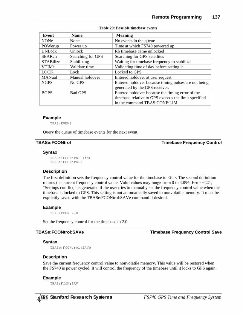
Remote Programming 137
Stanford Research Systems FS740 GPS Time and Frequency System
Table 20: Possible timebase events
Event Name Meaning NONe None No events in the queue POWerup Power up Time at which FS740 powered up UNLock Unlock Rb timebase came unlocked SEARch Searching for GPS Searching for GPS satellites STABilize Stabilizing Waiting for timebase frequency to stabilize VTIMe Validate time Validating time of day before setting it. LOCK Lock Locked to GPS MANual Manual holdover Entered holdover at user request NGPS No GPS Entered holdover because timing pulses are not being
generated by the GPS receiver. BGPS Bad GPS Entered holdover because the timing error of the
timebase relative to GPS exceeds the limit specified in the command TBAS:CONF:LIM.
Example TBAS:EVEN?
Query the queue of timebase events for the next event.
TBASe:FCONtrol Timebase Frequency Control
Syntax TBASe:FCONtrol <fc> TBASe:FCONtrol?
Description The first definition sets the frequency control value for the timebase to <fc>. The second definition returns the current frequency control value. Valid values may range from 0 to 4.096. Error −221, “Settings conflict,” is generated if the user tries to manually set the frequency control value when the timebase is locked to GPS. This setting is not automatically saved to nonvolatile memory. It must be explicitly saved with the TBASe:FCONtrol:SAVe command if desired.
Example TBAS:FCON 2.0
Set the frequency control for the timebase to 2.0.
TBASe:FCONtrol:SAVe Timebase Frequency Control Save
Syntax TBASe:FCONtrol:SAVe
Description Save the current frequency control value to nonvolatile memory. This value will be restored when the FS740 is power cycled. It will control the frequency of the timebase until it locks to GPS again.
Example TBAS:FCON:SAV
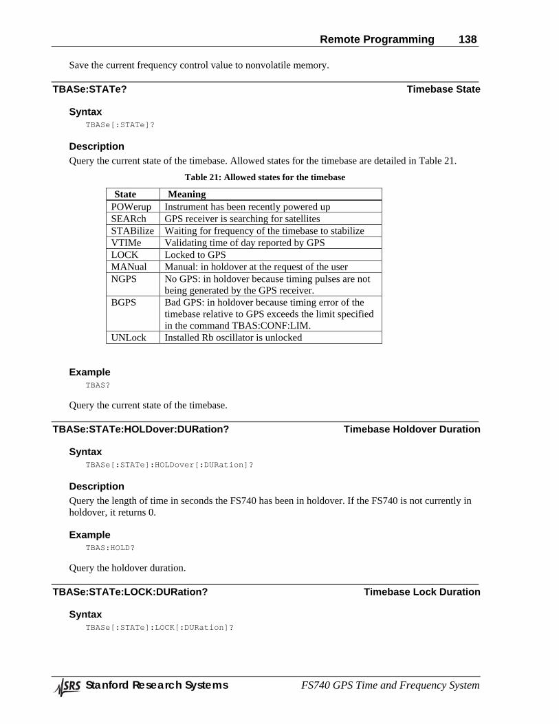
Remote Programming 138
Stanford Research Systems FS740 GPS Time and Frequency System
Save the current frequency control value to nonvolatile memory.
TBASe:STATe? Timebase State
Syntax TBASe[:STATe]?
Description Query the current state of the timebase. Allowed states for the timebase are detailed in Table 21.
Table 21: Allowed states for the timebase
State Meaning POWerup Instrument has been recently powered up SEARch GPS receiver is searching for satellites STABilize Waiting for frequency of the timebase to stabilize VTIMe Validating time of day reported by GPS LOCK Locked to GPS MANual Manual: in holdover at the request of the user NGPS No GPS: in holdover because timing pulses are not
being generated by the GPS receiver. BGPS Bad GPS: in holdover because timing error of the
timebase relative to GPS exceeds the limit specified in the command TBAS:CONF:LIM.
UNLock Installed Rb oscillator is unlocked
Example TBAS?
Query the current state of the timebase.
TBASe:STATe:HOLDover:DURation? Timebase Holdover Duration
Syntax TBASe[:STATe]:HOLDover[:DURation]?
Description Query the length of time in seconds the FS740 has been in holdover. If the FS740 is not currently in holdover, it returns 0.
Example TBAS:HOLD?
Query the holdover duration.
TBASe:STATe:LOCK:DURation? Timebase Lock Duration
Syntax TBASe[:STATe]:LOCK[:DURation]?
Remote Programming 139
Stanford Research Systems FS740 GPS Time and Frequency System
Description Query the length of time the FS740 has been locked to GPS. If the FS740 is not currently locked to GPS, it will return 0.
Example TBAS:LOCK?
Query the timebase lock duration.
TBASe:STATe:WARMup:DURation? Timebase Warm Up Duration
Syntax TBASe[:STATe]:WARMup[:DURation]?
Description Query the time in seconds that passed between when the FS740 was powered on and it first locked to GPS. If it has not successfully locked to GPS, then it returns the time in seconds since power on.
Example TBAS:WARM?
Query the warm up duration.
TBASe:TCONstant Timebase Time Constant
Syntax TBASe:TCONstant <time constant> TBASe:TCONstant? [CURRent|TARGet|MANual]
Description The first definition sets the time constant for the phase lock loop that locks the timebase to GPS when MANual is selected for the command TBASe:CONFig:BWIDth. The second definition queries one of three different time constants: the current time constant, the target time constant, and the manual time constant set with the first definition above. If the parameter is omitted, the current time constant is returned. If the timebase is configured for automatic bandwidth control (the default), the current time constant may vary from 3 s up to the target time constant for the installed timebase. The target time constant is a factory setting which identifies the optimum time constant for the installed timebase that should be used when the timebase has fully stabilized and timing errors are small.
Example TBAS:TCON 40 TBAS:TCON? TBAS:TCON? MAN
Set the manual time constant to 40 s. Query the current time constant. Query the manual time constant set above. It should be 40.
TBASe:TINTerval Timebase Time Interval
Syntax TBASe:TINTerval? [CURRent|AVERage]
Remote Programming 140
Stanford Research Systems FS740 GPS Time and Frequency System
Description Query the current or average measured time interval in seconds between the internal timebase and GPS. If the parameter is omitted, the current time interval is returned. The current time interval is the measured time interval between the internal timebase and the latest GPS timing pulse. The average time interval reported is an exponential average of the current time interval with a time constant equal to 1/6 of the time constant of the phase lock loop. See the TBASe:TCONstant command. Positive values indicate the internal timebase is lagging GPS. Negative values indicate the internal timebase is leading GPS. If time of day has not yet been set by the GPS receiver, this command generates error −230, “Data corrupt or stale.” Alternatively, if GPS is lost after time has been set, this command returns the last known time interval as the current time interval and zero for the average time interval.
Example TBAS:TINT?
Query the current time interval between the internal timebase and GPS.
Trigger Subsystem Commands in the Trigger Subsystem control the triggering of measurements. Normally when under local control, measurements are triggered continuously in order to provide continuous feedback while interacting with the instrument. Conversely, under remote control, measurements are only triggered when requested so that the data displayed corresponds closely with data retrieved. Commands in this subsystem enable the user to alter this behavior.
TRIGger:CONTinuous Trigger Continuous
Syntax TRIGger:CONTinuous [1|ON|0|OFF] TBASe:CONFig:BWIDth?
Description The first definition sets the desired trigger mode. The second definition queries the current trigger mode. When the parameter is omitted,
Example TBAS:CONF:BWID AUT
Configure the timebase to automatically increase bandwidth when timing errors are large and then gradually narrow the bandwidth when lock is stable.
Remote Programming 141
Stanford Research Systems FS740 GPS Time and Frequency System
Error Codes The instrument contains an error buffer that may store up to 10 error codes associated with errors encountered during power-on self tests, command parsing, or command execution. The ERR LED will be highlighted when a remote command fails for any reason. The errors in the buffer may be read one by one by executing successive SYST:ERR commands. The user may also view the errors from the front panel by navigating to Communication > Activity. Press CLEAR to discard the error. Errors are displayed in the order in which they occurred. The ERR LED will go off when all errors have been discarded.
The meaning of each of the error codes is described below.
Command Errors −100 Command Error
A nonspecific command error occurred.
−104 Data type error A parameter has the wrong data type.
−108 Parameter not allowed A parameter was supplied that is not allowed.
−109 Missing parameter A required parameter was missing.
−113 Undefined header The supplied command is undefined.
−114 Header suffix out of range A numeric suffix for one of the command keywords was out of range.
−120 Numeric data error A numeric value was supplied that could not be represented internally. This can happen if a number with an exponent larger than ±43 is supplied.
−131 Invalid suffix A supplied parameter contained invalid units.
−141 Invalid character data A supplied character data keyword was invalid or undefined.
−148 Character data not allowed The character data keyword supplied is defined but not allowed.
−151 Invalid string data The supplied string did not contain matched quotes.
Remote Programming 142
Stanford Research Systems FS740 GPS Time and Frequency System
−190 Command buffer overflow The supplied command exceeded 256 characters and the command buffer overflowed.
Execution Errors −200 Execution error
A nonspecific execution error occurred.
−213 Init ignored An INITiate command was received but a measurement was already in progress, so the command was ignored.
−221 Settings conflict A valid command was received, but it cannot be executed because current settings of the instrument are incompatible with the command. This may occur, for example, if one tries to manually set the frequency of the timebase when it is locked to GPS.
−222 Data out of range A supplied parameter is out of range.
−230 Data corrupt or stale An attempt to read data failed because it is already been discarded, corrupted, or lost.
Device Specific Errors −300 Device specific error
A device specific error occurred.
−314 Save/recall memory lost A *SAV or *RCL command failed because the settings stored in nonvolatile memory were corrupted or lost.
−350 Error queue overflow More have errors occurred, but they were discarded because the error queue overflowed.
−360 Communications error A framing or parity error occurred on the communications interface.
−363 Input buffer overrun The input buffer for the communications interface overflowed. All data was flushed and the communications interface reset.
−365 Time out error The instrument timed out waiting for data over the remote interface.
Query Errors −400 Query error
A nonspecific query error occurred.
Remote Programming 143
Stanford Research Systems FS740 GPS Time and Frequency System
−410 Query INTERRUPTED A new command was received before the previous query was read by the remote interface. The old query will be discarded.
−450 Query lost data The output buffer for the communications interface overflowed. The query result was discarded.
−451 Query no data The query resulted in no data.
Instrument Errors 500 GPS time out error
A command was sent to the GPS receiver, but the instrument time out waiting for a response.
501 GPS failed A command was sent to the GPS receiver, but the receiver rejected it as invalid.
514 Not allowed A command was received, but rejected not allowed because another remote interface has an exclusive lock on the instrument.
800 EEPROM read/write failed A read or write to nonvolatile EEPROM failed.
801 FPGA failed The FPGA failed to initialize.
900 Self test failed The instrument self test failed.
Remote Programming 144
Stanford Research Systems FS740 GPS Time and Frequency System
Example Programming Code The following program can be used as sample code for communicating with the instrument over TCP/IP. The program is written in the C++ language and should compile correctly on a Windows based computer. It could be made to work on other platforms with minor modifications. In order to use the program, you will need to connect the unit to your LAN and configure it with an appropriate IP address. Contact your network administrator for details on how to do this. To identify the unit’s current IP address from the front panel, navigate to Communication > TCP/IP Config. The current IP address will be displayed under Current Config.
Copy the program into a file named “fs740_ctrl.cpp”. To avoid typing in the program manually, download the electronic version of this manual from the SRS website (www.thinksrs.com). Select the program text and copy/paste it into the text editor of your choice. Compile the program into the executable “fs740_ctrl.exe”. At the command line type something like the following:
fs740_ctrl 192.168.0.5 where you should replace “192.168.0.5” with the IP address of the unit. You should see something like the following:
Connection Succeeded Stanford Research Systems,FS740,s/n001013,ver2.26.11 Closed connection
The program connects to the unit at the supplied IP address sets several parameters and then closes. If successful, the sine output frequency should be set to 1 MHz and the sine output voltage level should be set to 0.5 VPP.
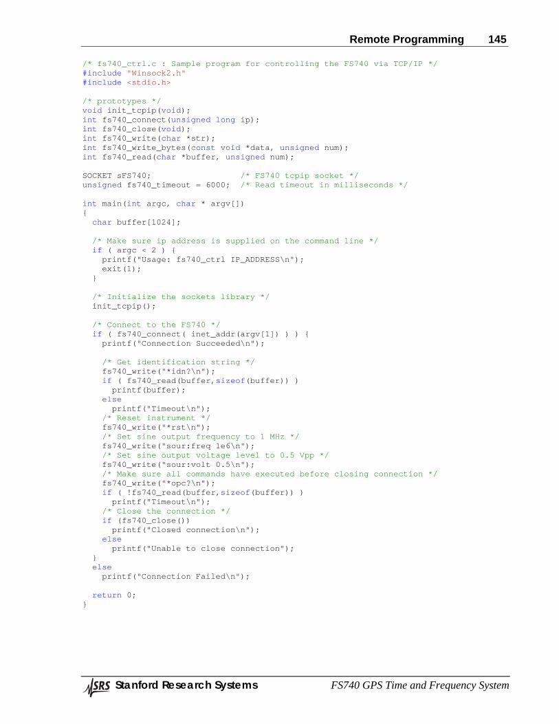
Remote Programming 145
Stanford Research Systems FS740 GPS Time and Frequency System
/* fs740_ctrl.c : Sample program for controlling the FS740 via TCP/IP */ #include "Winsock2.h" #include <stdio.h> /* prototypes */ void init_tcpip(void); int fs740_connect(unsigned long ip); int fs740_close(void); int fs740_write(char *str); int fs740_write_bytes(const void *data, unsigned num); int fs740_read(char *buffer, unsigned num); SOCKET sFS740; /* FS740 tcpip socket */ unsigned fs740_timeout = 6000; /* Read timeout in milliseconds */ int main(int argc, char * argv[]) char buffer[1024]; /* Make sure ip address is supplied on the command line */ if ( argc < 2 ) printf("Usage: fs740_ctrl IP_ADDRESS\n"); exit(1); /* Initialize the sockets library */ init_tcpip(); /* Connect to the FS740 */ if ( fs740_connect( inet_addr(argv[1]) ) ) printf("Connection Succeeded\n"); /* Get identification string */ fs740_write("*idn?\n"); if ( fs740_read(buffer,sizeof(buffer)) ) printf(buffer); else printf("Timeout\n"); /* Reset instrument */ fs740_write("*rst\n"); /* Set sine output frequency to 1 MHz */ fs740_write("sour:freq 1e6\n"); /* Set sine output voltage level to 0.5 Vpp */ fs740_write("sour:volt 0.5\n"); /* Make sure all commands have executed before closing connection */ fs740_write("*opc?\n"); if ( !fs740_read(buffer,sizeof(buffer)) ) printf("Timeout\n"); /* Close the connection */ if (fs740_close()) printf("Closed connection\n"); else printf("Unable to close connection"); else printf("Connection Failed\n"); return 0;
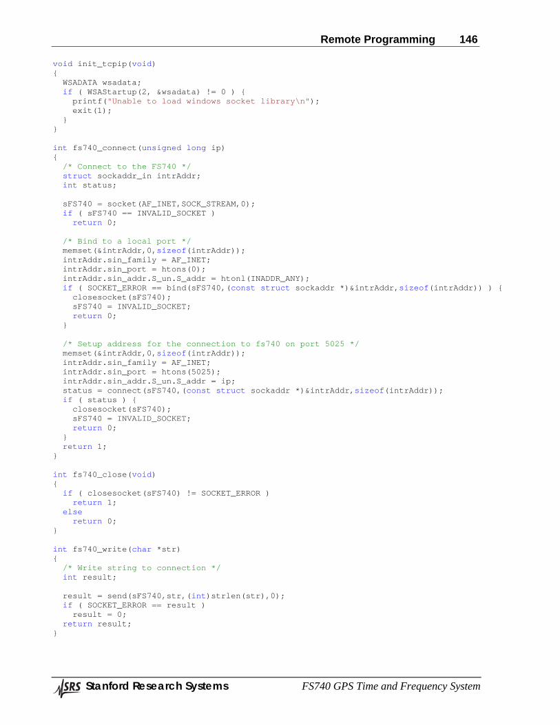
Remote Programming 146
Stanford Research Systems FS740 GPS Time and Frequency System
void init_tcpip(void) WSADATA wsadata; if ( WSAStartup(2, &wsadata) != 0 ) printf("Unable to load windows socket library\n"); exit(1); int fs740_connect(unsigned long ip) /* Connect to the FS740 */ struct sockaddr_in intrAddr; int status; sFS740 = socket(AF_INET,SOCK_STREAM,0); if ( sFS740 == INVALID_SOCKET ) return 0; /* Bind to a local port */ memset(&intrAddr,0,sizeof(intrAddr)); intrAddr.sin_family = AF_INET; intrAddr.sin_port = htons(0); intrAddr.sin_addr.S_un.S_addr = htonl(INADDR_ANY); if ( SOCKET_ERROR == bind(sFS740,(const struct sockaddr *)&intrAddr,sizeof(intrAddr)) ) closesocket(sFS740); sFS740 = INVALID_SOCKET; return 0; /* Setup address for the connection to fs740 on port 5025 */ memset(&intrAddr,0,sizeof(intrAddr)); intrAddr.sin_family = AF_INET; intrAddr.sin_port = htons(5025); intrAddr.sin_addr.S_un.S_addr = ip; status = connect(sFS740,(const struct sockaddr *)&intrAddr,sizeof(intrAddr)); if ( status ) closesocket(sFS740); sFS740 = INVALID_SOCKET; return 0; return 1; int fs740_close(void) if ( closesocket(sFS740) != SOCKET_ERROR ) return 1; else return 0; int fs740_write(char *str) /* Write string to connection */ int result; result = send(sFS740,str,(int)strlen(str),0); if ( SOCKET_ERROR == result ) result = 0; return result;
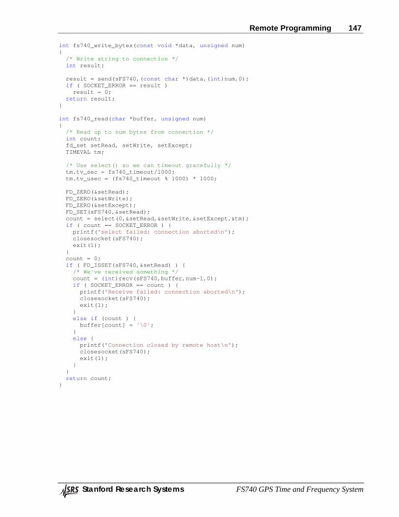
Remote Programming 147
Stanford Research Systems FS740 GPS Time and Frequency System
int fs740_write_bytes(const void *data, unsigned num) /* Write string to connection */ int result; result = send(sFS740,(const char *)data,(int)num,0); if ( SOCKET_ERROR == result ) result = 0; return result; int fs740_read(char *buffer, unsigned num) /* Read up to num bytes from connection */ int count; fd_set setRead, setWrite, setExcept; TIMEVAL tm; /* Use select() so we can timeout gracefully */ tm.tv_sec = fs740_timeout/1000; tm.tv_usec = (fs740_timeout % 1000) * 1000; FD_ZERO(&setRead); FD_ZERO(&setWrite); FD_ZERO(&setExcept); FD_SET(sFS740,&setRead); count = select(0,&setRead,&setWrite,&setExcept,&tm); if ( count == SOCKET_ERROR ) printf("select failed: connection aborted\n"); closesocket(sFS740); exit(1); count = 0; if ( FD_ISSET(sFS740,&setRead) ) /* We've received something */ count = (int)recv(sFS740,buffer,num-1,0); if ( SOCKET_ERROR == count ) printf("Receive failed: connection aborted\n"); closesocket(sFS740); exit(1); else if (count ) buffer[count] = '\0'; else printf("Connection closed by remote host\n"); closesocket(sFS740); exit(1); return count;

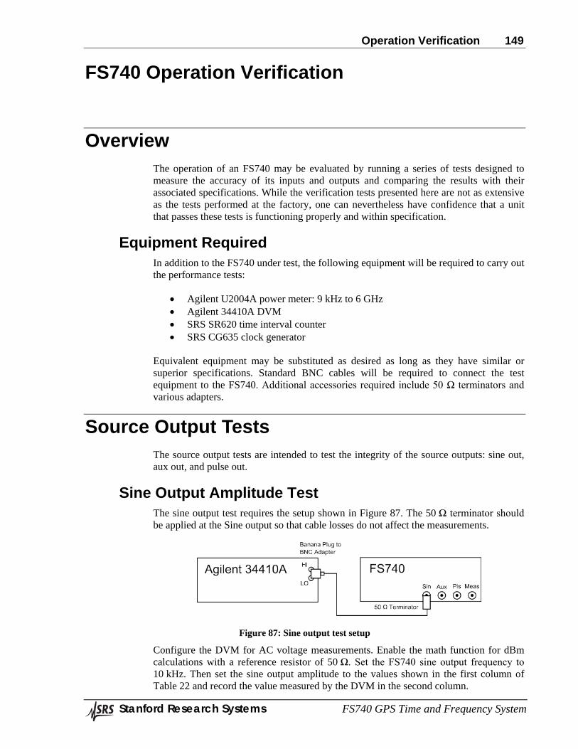
Operation Verification 149
Stanford Research Systems FS740 GPS Time and Frequency System
FS740 Operation Verification
Overview The operation of an FS740 may be evaluated by running a series of tests designed to measure the accuracy of its inputs and outputs and comparing the results with their associated specifications. While the verification tests presented here are not as extensive as the tests performed at the factory, one can nevertheless have confidence that a unit that passes these tests is functioning properly and within specification.
Equipment Required In addition to the FS740 under test, the following equipment will be required to carry out the performance tests:
• Agilent U2004A power meter: 9 kHz to 6 GHz • Agilent 34410A DVM • SRS SR620 time interval counter • SRS CG635 clock generator
Equivalent equipment may be substituted as desired as long as they have similar or superior specifications. Standard BNC cables will be required to connect the test equipment to the FS740. Additional accessories required include 50 Ω terminators and various adapters.
Source Output Tests The source output tests are intended to test the integrity of the source outputs: sine out, aux out, and pulse out.
Sine Output Amplitude Test The sine output test requires the setup shown in Figure 87. The 50 Ω terminator should be applied at the Sine output so that cable losses do not affect the measurements.
Figure 87: Sine output test setup
Configure the DVM for AC voltage measurements. Enable the math function for dBm calculations with a reference resistor of 50 Ω. Set the FS740 sine output frequency to 10 kHz. Then set the sine output amplitude to the values shown in the first column of Table 22 and record the value measured by the DVM in the second column.
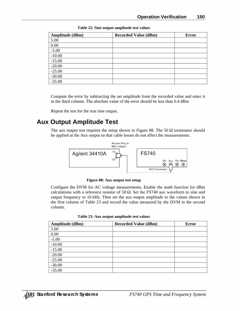
Operation Verification 150
Stanford Research Systems FS740 GPS Time and Frequency System
Table 22: Sine output amplitude test values
Amplitude (dBm) Recorded Value (dBm) Error 5.00 0.00 -5.00 -10.00 -15.00 -20.00 -25.00 -30.00 -35.00
Compute the error by subtracting the set amplitude from the recorded value and enter it in the third column. The absolute value of the error should be less than 0.4 dBm
Repeat the test for the rear sine output.
Aux Output Amplitude Test The aux output test requires the setup shown in Figure 88. The 50 Ω terminator should be applied at the Aux output so that cable losses do not affect the measurements.
Figure 88: Aux output test setup
Configure the DVM for AC voltage measurements. Enable the math function for dBm calculations with a reference resistor of 50 Ω. Set the FS740 aux waveform to sine and output frequency to 10 kHz. Then set the aux output amplitude to the values shown in the first column of Table 23 and record the value measured by the DVM in the second column.
Table 23: Aux output amplitude test values
Amplitude (dBm) Recorded Value (dBm) Error 5.00 0.00 -5.00 -10.00 -15.00 -20.00 -25.00 -30.00 -35.00
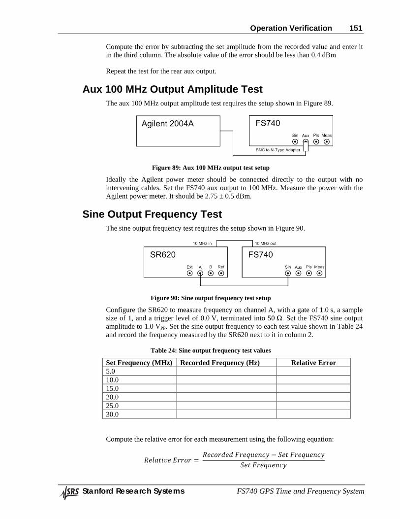
Operation Verification 151
Stanford Research Systems FS740 GPS Time and Frequency System
Compute the error by subtracting the set amplitude from the recorded value and enter it in the third column. The absolute value of the error should be less than 0.4 dBm
Repeat the test for the rear aux output.
Aux 100 MHz Output Amplitude Test The aux 100 MHz output amplitude test requires the setup shown in Figure 89.
Figure 89: Aux 100 MHz output test setup
Ideally the Agilent power meter should be connected directly to the output with no intervening cables. Set the FS740 aux output to 100 MHz. Measure the power with the Agilent power meter. It should be 2.75 ± 0.5 dBm.
Sine Output Frequency Test The sine output frequency test requires the setup shown in Figure 90.
Figure 90: Sine output frequency test setup
Configure the SR620 to measure frequency on channel A, with a gate of 1.0 s, a sample size of 1, and a trigger level of 0.0 V, terminated into 50 Ω. Set the FS740 sine output amplitude to 1.0 VPP. Set the sine output frequency to each test value shown in Table 24 and record the frequency measured by the SR620 next to it in column 2.
Table 24: Sine output frequency test values
Set Frequency (MHz) Recorded Frequency (Hz) Relative Error 5.0 10.0 15.0 20.0 25.0 30.0
Compute the relative error for each measurement using the following equation:
𝑅𝑒𝑙𝑎𝑡𝑖𝑣𝑒 𝐸𝑟𝑟𝑜𝑟 = 𝑅𝑒𝑐𝑜𝑟𝑑𝑒𝑑 𝐹𝑟𝑒𝑞𝑢𝑒𝑛𝑐𝑦 − 𝑆𝑒𝑡 𝐹𝑟𝑒𝑞𝑢𝑒𝑛𝑐𝑦
𝑆𝑒𝑡 𝐹𝑟𝑒𝑞𝑢𝑒𝑛𝑐𝑦
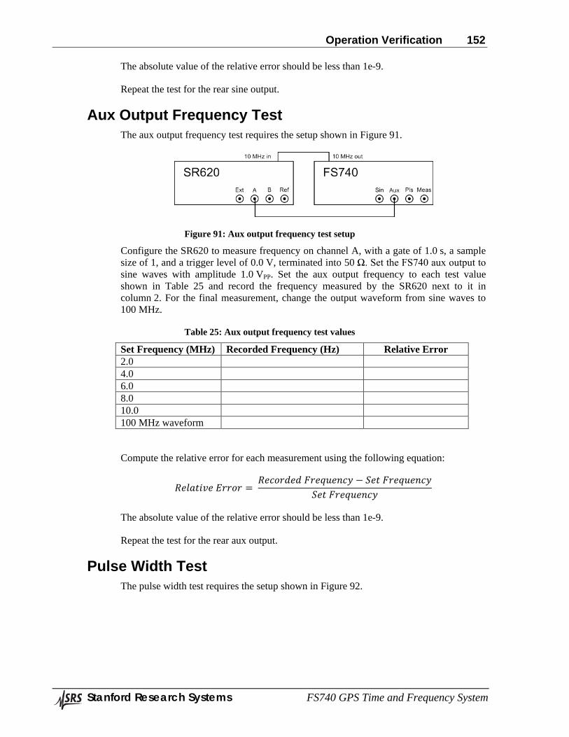
Operation Verification 152
Stanford Research Systems FS740 GPS Time and Frequency System
The absolute value of the relative error should be less than 1e-9.
Repeat the test for the rear sine output.
Aux Output Frequency Test The aux output frequency test requires the setup shown in Figure 91.
Figure 91: Aux output frequency test setup
Configure the SR620 to measure frequency on channel A, with a gate of 1.0 s, a sample size of 1, and a trigger level of 0.0 V, terminated into 50 Ω. Set the FS740 aux output to sine waves with amplitude 1.0 VPP. Set the aux output frequency to each test value shown in Table 25 and record the frequency measured by the SR620 next to it in column 2. For the final measurement, change the output waveform from sine waves to 100 MHz.
Table 25: Aux output frequency test values
Set Frequency (MHz) Recorded Frequency (Hz) Relative Error 2.0 4.0 6.0 8.0 10.0 100 MHz waveform
Compute the relative error for each measurement using the following equation:
𝑅𝑒𝑙𝑎𝑡𝑖𝑣𝑒 𝐸𝑟𝑟𝑜𝑟 = 𝑅𝑒𝑐𝑜𝑟𝑑𝑒𝑑 𝐹𝑟𝑒𝑞𝑢𝑒𝑛𝑐𝑦 − 𝑆𝑒𝑡 𝐹𝑟𝑒𝑞𝑢𝑒𝑛𝑐𝑦
𝑆𝑒𝑡 𝐹𝑟𝑒𝑞𝑢𝑒𝑛𝑐𝑦
The absolute value of the relative error should be less than 1e-9.
Repeat the test for the rear aux output.
Pulse Width Test The pulse width test requires the setup shown in Figure 92.
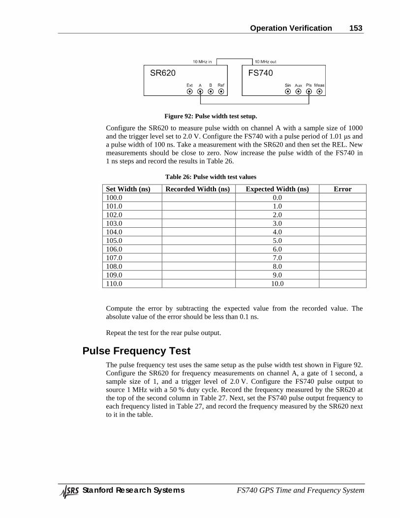
Operation Verification 153
Stanford Research Systems FS740 GPS Time and Frequency System
Figure 92: Pulse width test setup.
Configure the SR620 to measure pulse width on channel A with a sample size of 1000 and the trigger level set to 2.0 V. Configure the FS740 with a pulse period of 1.01 μs and a pulse width of 100 ns. Take a measurement with the SR620 and then set the REL. New measurements should be close to zero. Now increase the pulse width of the FS740 in 1 ns steps and record the results in Table 26.
Table 26: Pulse width test values
Set Width (ns) Recorded Width (ns) Expected Width (ns) Error 100.0 0.0 101.0 1.0 102.0 2.0 103.0 3.0 104.0 4.0 105.0 5.0 106.0 6.0 107.0 7.0 108.0 8.0 109.0 9.0 110.0 10.0
Compute the error by subtracting the expected value from the recorded value. The absolute value of the error should be less than 0.1 ns.
Repeat the test for the rear pulse output.
Pulse Frequency Test The pulse frequency test uses the same setup as the pulse width test shown in Figure 92. Configure the SR620 for frequency measurements on channel A, a gate of 1 second, a sample size of 1, and a trigger level of 2.0 V. Configure the FS740 pulse output to source 1 MHz with a 50 % duty cycle. Record the frequency measured by the SR620 at the top of the second column in Table 27. Next, set the FS740 pulse output frequency to each frequency listed in Table 27, and record the frequency measured by the SR620 next to it in the table.
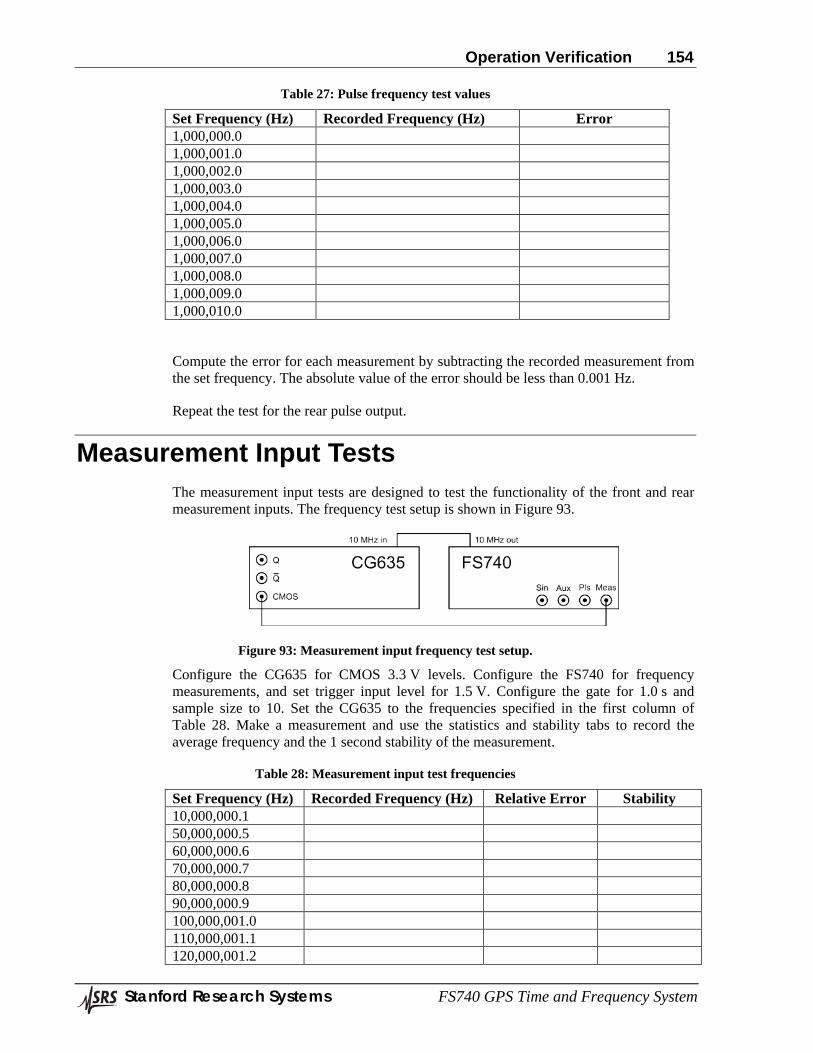
Operation Verification 154
Stanford Research Systems FS740 GPS Time and Frequency System
Table 27: Pulse frequency test values
Set Frequency (Hz) Recorded Frequency (Hz) Error 1,000,000.0 1,000,001.0 1,000,002.0 1,000,003.0 1,000,004.0 1,000,005.0 1,000,006.0 1,000,007.0 1,000,008.0 1,000,009.0 1,000,010.0
Compute the error for each measurement by subtracting the recorded measurement from the set frequency. The absolute value of the error should be less than 0.001 Hz.
Repeat the test for the rear pulse output.
Measurement Input Tests The measurement input tests are designed to test the functionality of the front and rear measurement inputs. The frequency test setup is shown in Figure 93.
Figure 93: Measurement input frequency test setup.
Configure the CG635 for CMOS 3.3 V levels. Configure the FS740 for frequency measurements, and set trigger input level for 1.5 V. Configure the gate for 1.0 s and sample size to 10. Set the CG635 to the frequencies specified in the first column of Table 28. Make a measurement and use the statistics and stability tabs to record the average frequency and the 1 second stability of the measurement.
Table 28: Measurement input test frequencies
Set Frequency (Hz) Recorded Frequency (Hz) Relative Error Stability 10,000,000.1 50,000,000.5 60,000,000.6 70,000,000.7 80,000,000.8 90,000,000.9 100,000,001.0 110,000,001.1 120,000,001.2
Operation Verification 155
Stanford Research Systems FS740 GPS Time and Frequency System
Compute the relative error for each measurement using the following equation:
𝑅𝑒𝑙𝑎𝑡𝑖𝑣𝑒 𝐸𝑟𝑟𝑜𝑟 = 𝑅𝑒𝑐𝑜𝑟𝑑𝑒𝑑 𝐹𝑟𝑒𝑞𝑢𝑒𝑛𝑐𝑦 − 𝑆𝑒𝑡 𝐹𝑟𝑒𝑞𝑢𝑒𝑛𝑐𝑦
𝑆𝑒𝑡 𝐹𝑟𝑒𝑞𝑢𝑒𝑛𝑐𝑦
The absolute value of the relative error should be less than 1e-11. The recorded stability should be less than 1e-10.
Repeat the test for the rear measurement input.
Conclusions The tests described in this document are designed to test the basic functionality of the unit. They are not intended to be a substitute for the complete performance test which is performed at the factory. Nevertheless, one can have reasonable confidence that instruments that pass the tests described in this document are operating correctly. As always, if an instrument fails to pass a test, verify that the setup has been duplicated correctly, and that the individual procedures have been followed as specified. Instruments that have failed to meet specifications may be returned to SRS for repair.

Circuit Description 157
Stanford Research Systems FS740 GPS Time and Frequency System
FS740 Circuit Description
Overview The FS740 provides a 10 MHz frequency reference which is disciplined by GNSS with a long term stability of better than 1:1013. The instrument can also time tag external events with respect to UTC or GNSS and measure the frequency of user inputs. The instrument also has DDS synthesized frequency outputs, adjustable rate (and width) pulse outputs, and an AUX output for arbitrary waveforms including an IRIG-B timecode output. A GUI (graphical user interface) allows the user to configure the instrument and see the results of time and frequency measurements.
The performance of the 10 MHz output depends on the installed timebase. The standard timebase provides 1:109 short term frequency stability and phase noise of less than −100 dBc/Hz at 10 Hz offset. An optional OCXO (ovenized crystal oscillator) timebase provides 1:1011 short term frequency stability and phase noise of less than −130 dBc/Hz at 10 Hz offset. An optional rubidium timebase provides 1:1012 short term frequency stability, phase noise of less than −130 dBc/Hz at 10 Hz offset, and a long term holdover (lost GNSS signal) of better than 1 μs/day.
Either optional timebase (OCXO or rubidium) provides a dramatic improvement in the holdover characteristics, a 30 dB reduction in the phase noise and a tenfold reduction in the TDEV. There are some users who would not need this performance improvement. For example, users who only need time tags with 1μs accuracy or frequency measurements with 1:108 accuracy could use the standard timebase.
The FS740 provides bias for a remote active GNSS antenna. The unit’s GNSS receiver tracks up to 12 satellites, will automatically survey and fix its position, then use all received signals to optimize its timing solution. The FS740 time-tags the 1 pps output from the receiver, corrects the result for the receiver’s sawtooth error, then phase locks the timebase to the GNSS 1 pps with an adjustable time constant between 10 seconds and 4000 s. The TDEV (rms timing deviation) between two instruments is a few nanoseconds.
If the GNSS signal is lost, the timebase is left at the last locked frequency value. The timebase will age or drift in frequency by up to ±2 ppm (for the standard timebase), ±0.05 ppm/year and ±0.002 ppm (0 to 45⁰C) for the OCXO, and ±0.001 ppm/year and ±0.0001 ppm (0 to 45⁰C) for the rubidium timebase.
There are two user inputs (one on the front, one on the rear panel) for frequency and time tag events. The inputs have adjustable thresholds and slopes. Frequencies are measured with a precision of 1:1011 in 1 s, 1:1012 in 10 s, and 1:1013 in 100 s. Time tags are reported with 1 ps resolution commensurate with the short term stability of the OCXO and rubidium timebases. Time tags will have an error of about 10 ns rms with respect to UTC or GNSS time.
The FS740 has a rear panel low phase noise 10 MHz sine output with an amplitude of 1 Vrms. Up to 15 additional copies of the 10MHz output are available via optional rear panel outputs.
Circuit Description 158
Stanford Research Systems FS740 GPS Time and Frequency System
The FS740 has front and rear panel sine outputs which provide sine outputs from 1 mHz to 30.1 MHz with 1 μHz resolution, or a fixed 100 MHz, with adjustable amplitude from 100 mV to 1.2 V rms. Up to 15 additional copies of the sine outputs are available via optional rear panel outputs.
The FS740 has front and rear panel pulse outputs which can provide low jitter pulses from 1 mHz to 25 MHz. The pulse outputs have adjustable phase with respect to UTC and the pulse width can be set as narrow as 5 ns, or as wide as the entire pulse period minus 5 ns, with 1 ps resolution. Up to 15 additional copies of the pulse outputs are available via optional rear panel outputs.
The FS740 has front and rear panel auxiliary (aux) output which can generate standard or arbitrary waveforms (sine, ramp, triangle, etc.) The aux output can also provide an AM modulated IRIG-B timecode output. Up to 15 additional copies of the aux output are available via optional rear panel outputs.
A rear panel alarm relay is set if power is lost or under user defined conditions including: timebase fault, loss of GNSS reception, or any failure to maintain phase lock between the timebase and GNSS. The relay has both normally open and closed outputs.
Optional distribution amplifiers, each providing five additional rear panel outputs for the 10 MHz, SINE, PULSE, AUX or IRIG-B outputs, can be installed. Up to three distribution amplifiers can be installed and configured from the front panel. Each output has its own driver which provides high isolation between outputs.
The instrument may be used without GNSS. The (optional) rubidium timebase has a lifetime aging of only a few parts per billion, and can serve as an autonomous laboratory timebase in many applications.
Sub-Systems The FS740 has five sub-systems: The front panel, the motherboard, the power supply, the (optional), rear-panel distribution amplifiers and the (optional) timebase. When reading circuit descriptions it is useful to know that the first digit of a component reference is the same as the sheet number in the schematics. Hence, R321 would be found on the third schematic sheet of a particular sub-assembly.
Front panel The main display is a 480x272 color TFT LCD with white backlights and a capacitive touch screen. The front panel PCB uses a 32-bit ARM MPU (U105, an LPC1788FBD208) to drive the LCD, interpret touch screen commands, and send commands to the motherboard. A USB port, which was used during product development and may be used in future products, is not used in the FS740.
There are two large memories on the front panel PCB. A 32 x 8M dynamic RAM and a 16 x 16M flash. The flash is primarily used for display fonts, and the RAM is used as program memory and as 512k sample storage for the motherboard.
The front panel controls the FS740 very much like a remote computer would do. For example, when a user enters a frequency for the SINE output, the front panel MPU displays the number as it is being entered, and sends a command to the motherboard to
Circuit Description 159
Stanford Research Systems FS740 GPS Time and Frequency System
change the frequency only after the User presses the Enter key. Similarly, if the User asks to see the result of a frequency measurement, the front panel sends a query to the motherboard, the motherboard responds with the result, and the front panel MPU displays it.
The interface between the front panel and the motherboard is via the 16 pin header, J201. There is a LVDS pair with the 10 MHz frequency reference passed up from the motherboard on J201. A line receiver, U201, converts this to a CMOS logic level. The MPU’s 12 MHz clock is phase locked to the 10 MHz reference to avoid clock-walk interference between the display PCB and the motherboard. The MPU provides 10 MHz to the phase detector from one of its PWMs. The PLL consists of a phase detector (U104), a LPF (R114, R116 and C125), and a varactor (D105).
A switch-mode boost regulator provides about 40 mA at about 19.2 V to power the display backlight LEDs. The regulator operates at nominal 1 MHz switching frequency, and has under voltage lockout, and over voltage and thermal protection.
Motherboard 10 MHz, 20 MHz and 100 MHz Page 1
A temperature controlled 20 MHz timebase is the reference source used in all instrument configurations. A 20 MHz, 3rd overtone, AT-cut resonator (Y100) is operated in a Colpitts oscillator, with an NPN transistor (Q102) as the active element. The bias current and voltage of Q102 are carefully controlled to reduce drift and aging. The bias voltage to the collector of Q102 is set by the +4.096 systems voltage reference, reduced by the base-emitter drop of Q101. The collector bias currents are maintained at 4 mA by U101 (operating as an integrator) which controls the base current to Q102 via the 100 kΩ resistor, R118. U101 servos the voltage drop across the 1.00 kΩ shunt resistor (R104) to the +4.096 V system voltage reference.
The temperature of the 20 MHz oscillator is controlled to about 55 C, which is the upper turning point for the 3rd OT, AT-cut resonator. The temperature controller consists of an NTP thermistor (R120), an integrator (U104B), a level shifter (U104A), and two heaters (U100 and Q100).
The 20 MHz sine across L102 is amplified by U106, and limited by U110, to produce a clean 20 MHz square wave. The 20 MHz square wave is used as the reference to the 100 MHz PLL. It is also divided by two to generate a 10 MHz square wave to clock three hex buffers. All of the hex buffers drive the primary of RF transformers (T101-T103) that have 2:1 turn ratios, matching 50 Ω loads to the 200 Ω source. One of the RF transformer outputs drives an analog mixer, which is part of the PLL which locks the 20 MHz Colpitts oscillator to an optional timebase. Two of the RF transformer outputs are filtered by 5th order Cauer low pass filters (11 MHz) that have notches at 30 MHz. One of these filters drives the rear panel 10 MHz sinewave output, the other is the source for the 10 MHz optional rear panel distribution amplifiers.
The varactor frequency control (D101) for the 20 MHz reference oscillator is provided by either the high resolution DAC (BIG_DAC) or, in the case of an installed optional timebase, by the output of the PLL integrator, U102B. The logic signal DAC/-PLL determines the source. When DAC/-PLL is low, the input to the integrator comes from
Circuit Description 160
Stanford Research Systems FS740 GPS Time and Frequency System
the phase detector, U105, which is a +13 dBm level doubly-balanced diode mixer. When DAC/-PLL is high, the output of the PLL integrator is servo’d to BIG_DAC.
The reference frequency for the 20 MHz oscillator PLL comes from one of the optional timebases (either a 10 MHz OCXO or a rubidium frequency standard). The optional timebase is held with a bracket, and plugs into the motherboard via the 10-pin header, J100. The presence and type of optional oscillator is automatically detected by the motherboard.
The instrument uses a 100 MHz timebase for all timing functions. A 100 MHz VCXO (U119) is phase locked to the 20 MHz crystal timebase (which may itself be phase locked to an optional OCXO or rubidium frequency standard). A five channel ECL driver (U120) provides five source terminated, 100 Ω, LVDS 100 MHz system clocks (for the waveform DACs, FPGA, CPU, time-tagging TACs, and the pulse generator). The 100 MHz can also be sourced as an AUX output when U116 drives a 120 MHz low-pass filter (with notches at 200 MHz and 300 MHz). This 100 MHz sinewave is transformed into a balanced signal by T103 that is sourced and terminated by 100 Ω.
GNSS Timing Receiver and Time-Tagging Page 2 An OEM GNSS timing receiver is used to provide GNSS and GLONASS timing as a 1 pps pulse and a serial message. The timing receiver, U206, requires an active antenna. Bias current, short-circuit current protection, and current monitoring for the antenna is provided by U201, U201 and Q203. The dc bias is decoupled from the satellite signals (1575.42 MHz for GNSS) by L204, a 0.12 μH inductor which is self-resonant near that frequency.
The TPS2030 is a 33 mΩ high-side MOSFET switch that limits the antenna bias current to 300 mA. The device also has a thermal shutdown and an overcurrent logic output. The antenna current is measured with the 1 Ω shunt resistor, R213. A current mirror, U201 and Q203, cascodes 1% of the antenna current into R217, providing a voltage of 1 V per 100 mA of antenna current for measurement by the MPU’s ADC.
The 1 pps output from the GNSS timing receiver is aligned with UTC and time-tagged with sub-picosecond resolution. One of two inputs can be selected as the input to the time-tagging circuit by U211: A calibration signal, ±CAL_TRIG1 or the 1 pps from the timing receiver. The selected signal is converted to LVDS by U213 and transmitted to the time-tagging input, U214. The rising edge of the output of U214 is the time-tagged event.
A 100 MHz free running counter in the FPGA (Sheet 4) is used to time-tag events with 10 ns of resolution (digital time). A time-to-amplitude converter (TAC) is used to measure the time between the event and the second edge of the 100 MHz clock after the event (an interval between 10 ns and 20 ns). The output of the TAC is digitized, scaled, offset and subtracted from the digital time to provide a time tag with picosecond resolution.
The time-tagging circuit has several requirements: To provide a SYNC clock to the FPGA with has been re-sync’d to the 100 MHz system clock. To enable a current source for the interval between the event and the second 100 MHz clock edge after the event. To integrate the current and so convert the time interval to a voltage. And to be reset prior to the next event.
Circuit Description 161
Stanford Research Systems FS740 GPS Time and Frequency System
There are four D-type flip flops which are part of the time-tagging circuit. These are very fast CMOS flip-flop, operated from +2.5 V, and with CLK-Q propagation delays between 0.5 ns and 1.4 ns. The first two (U207 and U208) are clocked by the event, and the event delayed by about 4 ns. The last two flip-flops (U209 and U210) are clocked by the 100 MHz system clock. An important part of the design methodology is the avoidance on metastability (the modulation of the propagation delay from the clock input to the data output when the clock edge is close to a change in data, set, or reset inputs).
The first flip-flop (U207) is clocked by the event input. It is possible that the CLR input to this flip-flop was just removed, and so to avoid metastability problems, the output of the first flip-flop is resynchronized by clocking a second flip-flop (U208) with the delayed event. The output of the second flip-flop is synchronous with the event and free of any metastability artifacts. This output is used to start the TAC interval, by pulsing the analog integrator reset (U204) high, reverse biasing D200, and allowing the integrator current (from Q201B) to start charging C203.
The output of the second flip-flop is clocked serially into the third flip-flop (U209) and the fourth (U210). The output of the fourth flip-flop stops the TAC interval by turning off the current from Q201B. The double resynchronization serves two purposes: to remove the metastability between the event and the 100 MHz clock, and to make the minimum TAC interval 10 ns.
The integrator’s current source is controlled by U200 and Q200. The feedback network provides a virtual null to the op amp inputs when +4.096/2 is across the 200 Ω shunt resistor, R201. The current through the shunt, about 10.24 mA, is cascoded through Q200. The collector current from Q200 is switched between Q201A and Q201B under the control of the flip-flop U210.
During the TAC interval, the current integrates on C203. The voltage on C203 is buffered by U203, a fast FET input op amp configured with a gain of two. The output of the buffer amp is digitized by U403 (Sheet 4). The output voltage has a scale factor of about 2 V/ 10 ns. The +4.096 V full-scale 16-bit ADC provides a timing resolution of about 0.3 ps. The TAC voltage is a measure of the time between the event and the second clock edge of the 100 MHz system clock.
The integrator is reset by U204. When the time-tagger is reset from the prior event, the first flip-flop (U207) is cleared by EN_TAG1 going low. The Q output from U207 clears the other three flip-flops, returning the non-inverting input of U204 to ground. The diode, D201, is biased with about 10 mA of current, creating a voltage of about +0.7 V. The op amp has a gain of minus one, and so its output is at about -0.7 V, compensating for the voltage drop across D200. The integrating capacitor, C203, will be reset to about +0.5 V (the voltage across R221 with 10 mA passing though it). The RC time-constant is about 5 ns.
Front and Rear Panel Time-Tags Page 3 There are three time-tagging channels in the FS740. The first, described above, is dedicated to time-tagging the GNSS 1 pps output. The other two are general purpose time-taggers available to the user via front and rear panel BNC “MEASURE” inputs. These inputs can be used to time-tag events with respect to UTC or to measure frequency and frequency stability.
Circuit Description 162
Stanford Research Systems FS740 GPS Time and Frequency System
The input discriminators for these time-tagging channels are located on Sheet 7 of the motherboard schematics. The dc coupled, 1 MΩ/22 pF, input comparators can be selected and have their outputs converted to LVDS. (Calibration timing signals can also be selected. They are the LVDS signals ±CAL_TRIG2 and ±CAL_TRIG3. These signals are used to determine offsets and scale factors for the TACs which are part of the time-tagging circuits.)
The time-tagging circuitry for the front and rear panel are very similar to that used for the GNSS time-tagging, except they are designed to support a high conversion rate. For example, when measuring 100 MHz, each cycle of the 100 MHz signal is counted by the FPGA via the ±CNT2 or ±CNT3 LVDS signals, and time-tags of particular zero crossings can be made every 16 μs.
FPGA Page 4 A 250,000 gate Xilinx FPGA, operating from +3.3 V, +2.5 V, and +1.2 V, is used to time-tag events and generate output waveforms. The FPGA is clocked at 100 MHz and is serially connected to a 16-bit ADC (to digitize the TACs, etc.) and to the MPU. The serial interface between the MPU and the FPGA allows the MPU to program, control, and read data from the FPGA.
A free running counter on the FPGA, clocked at 100 MHz, can be latched by any of three SYNC inputs to provide the digital portion of the time-tag. Three asynchronous CNT inputs clock counters and can be latched by their corresponding TAG inputs. The CNT inputs are used to count cycles of a frequency source, which together with time-tags, provide high resolution frequency measurements.
A 16-bit ADC is serially interfaced to the FPGA. The ADC is read constantly to digitize the TACs, which provide the analog portion (0-10 ns) of the time-tags. The ADC operates for an internal +4.096 V voltage reference.
The FPGA provides parallel data to four 14-bit DACs at a 100 MHz sample rate. The AUX data is used to generate the analog AUX output (sine, triangle, square, and AM IRIG-B). The FREQ data is used to generate a sine wave output between 0.001 Hz and 30.1 MHz. The START and STOP data are used to adjust the timing of the leading and trailing pulse output edges allowing any pulse frequency from 0.001 Hz to 25 MHz. The FPGA also provides the counting logic and outputs to control the pulse generator and time-tagging circuitry.
Fast Analog Waveforms Page 5 Four 14-bit DACs, updated by the FPGA at a 100 MHz sample rate, are shown on Sheet 5. DAC outputs for the SINE and AUX outputs are filtered for waveform reconstruction. The SINE waveform is filtered with a differential, 7th order, Cauer low pass filter, with a 33 MHz passband and >80 dB attenuation above 65 MHz. The AUX output is filtered with a differential, 7th order, Bessel low pass filter with a 12 MHz passband and 90 dB attenuation at 90 MHz. All filters have a 200 Ω source and load termination, and each drives three differential buffer amplifiers (AD8131s). The differential buffer amplifiers pass copies of the analog waveforms to the front, rear, and optional rear panel outputs.
Both the SINE and AUX DACs have their own amplitude control. The 12-bit system DAC (U818 on Sheet 8) provides FREQ_AMPL and AUX_AMPL which program the DAC set currents to control the amplitude. Both halves of the op amp, U508, are
Circuit Description 163
Stanford Research Systems FS740 GPS Time and Frequency System
operated with a gain of 3x. Increasing FREQ_AMPL or AUX_AMPL drives the corresponding output lower, increasing the current through the programming resistors (R523 and R530), and so increasing the output amplitude.
Two of the 14-bit DACs provide agile, unfiltered, differential waveforms with a 100 Ω source impedance. These waveforms are used to control the timing of the leading (start) and trailing (stop) edges of the PULSE generator output. The pulse generator can be operated at any frequency between 0.001 Hz and 25 MHz. The timing of each pulse edge is controlled by the FPGA, which determines both the analog (0-10 ns) and digital (n x 10 ns) timing of both leading and trailing edges of the pulse output.
Agile Pulse Generator Page 6 The term “agile” refers to the ability of the pulse generator to determine the timing of each pulse generator edge on-the-fly. Certain pulse generator frequencies are easy to generate from a fixed 100 MHz system clock. For example, a 1 MHz output is had by simply dividing the system clock by 100. Other frequencies require more work. For example, a 9 MHz output has a period of 111.111111 ns. To arrange this we would count 11 cycles of the 100 MHz clock (for 110 ns of delay) and increase the analog delay by 1.111111 ns for each cycle. After 9 cycles, the analog delay would return to zero and we increase the cycle count to 12 for just one period. All this is computed and controlled by the FPGA in real time.
The agile characteristic make it easy to adjust the phase of the pulse generator output, for example, to align the leading edge to UTC. It also allows any frequency to be generated, not just submultiples of the 100 MHz system clock. Further, it allows an unlimited duty cycle range for the output pulse. The only significant downside is jitter, which can be as large as 50 ps rms for outputs which are not submultiples of the 100 MHz system clock.
The pulse generator output is the XOR (U614) between the DELAYED_START (U606) and the DELAYED_STOP (U626). The start and stop are initiated by PULSE_START and PULSE_STOP, which are 20 ns logic signals from the FPGA. The circuits for the START and STOP channels are virtually the same, and so only the START path will be described.
The pulse is initiated when the FPGA asserts PULSE_START. This signal is re-sync’d to the 100 MHz system clock by the flip-flop, U602. When the Q output from U602 goes high (to +2.5 V) the output of the op amp, U600A with a gain of 2x, goes down by 5.0 V. This reverse biases D600, which had been holding the integrating capacitor (C609) in it preset condition (a diode drop below +8.192 V). The constant current source (Q603) linearly discharges C609.
The differential pair, Q602A and Q602B, are used as a fast, low gain comparator. When the voltage on C609 ramps down to the output of U611 (which is controlled by the 14-bit START_DAC), the comparator will cross over, clocking U606 via U608, and so asserting the DELAYED_START.
The analog delay span is adjusted to exactly 10 ns via CAL_START’s control of the constant current source which controls the ramp speed on C609. In this way, the resolution of the analog delay is about 10 ns / 214 = 0.61 ps.
The XOR output, U614, is high for the interval between the DELAYED_START and the DELAYED_STOP. When DELAYED_STOP is asserted, an 8 ns reset pulse, -EOC,
Circuit Description 164
Stanford Research Systems FS740 GPS Time and Frequency System
is generated by U633, which resets both flip-flops (and de-glitches the XOR output as the flip-flops are reset). The XOR output can be held off by PULSE_EN (U618) or inverted by PULSE_INV (U617).
Three LVDS copies of the pulse output are generated by U603, U612, and U609, for the front, rear and optional outputs. Output drivers for the front PULSE output consists of an LVDS line receiver (U604), a 0.7 V offset source (Q601), a delay equalizer (U630) and an output driver (U601). The output source impedance is about 50 Ω, and the output pulse shape is improved with the C602/L600/R600/C600 network. The rear panel PULSE output is the same.
By enabling EN_PULSE_CAL, which sources the pulse generator to the time-tagging TACs, the two systems can be used to calibrate each other. For both circuits, it is important to calibrate the full scale analog delay, or analog time-tag, to be 10 ns. When the pulse generator output is being measured by the time-tagger, the value of the CAL_START DAC is adjusted until the full scale analog delay is equal to the duration of one 100 MHz clock cycle. Similarly, by adjusting the pulse generator output to a boundary of a 100 MHz clock cycle, the full scale span of the TAC can be measured.
Inputs and Outputs Page 7 There are two identical input discriminators, one for the front panel and one for the rear. The front panel circuit will be described here. The front panel MEASURE input BNC has an input impedance modeled by 1 MΩ in parallel with 22 pF. The high impedance, dc coupled, input network attenuates the signal by ½, and level shifts the input by +2 V. The current from the level shifter is balanced by an equal and opposite current through R708, so that no level shift is seen at the BNC input to the instrument. The attenuated and shifted input is compared to the FRONT_LVL DAC voltage by U701, whose output can be inverted, or not, by U702. The output of U702 can be selected to drive an LVDS transmitter to drive the time-tagging input on Sheet 3.
Four differential analog line receivers and output drivers (U700, U706, U713, and U714) are used to drive the front and rear panel SINE and AUX outputs. The line receivers provide a high CMRR, some gain, drive the output via a 50 Ω series resistor. The output amplitude, terminated into 50 Ω, can be set between 10 mVpp and 1.414 Vpp. (Output amplitudes double when unterminated.)
The interface to the optional rear panel outputs is via J706. Three different distribution amplifiers are available, and each has 5 identical outputs. Opt A provides 10 MHz outputs (typically used to provide external 10 MHz inputs to other instruments). Opt B provides either SINE or AUX outputs. Opt C provides +5 V pulse outputs (or +2.5 V into 50 Ω). The FS740 automatically identifies what type card populates each of the three available rear panel slots.
Microcontroller Page 8 The instrument uses an MCF52235CAL60 microcontroller (MPU). The part has internal RAM, ROM, SPI, UART, and Ethernet interfaces. Most peripherals are communicated with via the SPI. The SPI addresses are split into two domains. The Noisy Domain is for parts (such as memory) which are tolerant of clock and data noise when the SPI is communicating to other devices. The Quiet Domain is for devices which cannot tolerate the interference from an active SPI bus when they are not being addressed (such as PLL

Circuit Description 165
Stanford Research Systems FS740 GPS Time and Frequency System
synthesizers). The Quiet Domain’s SPI CLK and DATA are gated off when not addressing a device in the Quiet Domain.
The MPU operates from +3.3 V using a 25 MHz clock. The 25 MHz clock is derived by dividing the 100 MHz system clock by four with U812 and U813. An 8 MB serial flash memory is connected to the MPU via the SPI. This memory holds the configuration data for the FPGA.
A very quiet 16-bit DAC (U819, an AD5760) provides a low noise, high resolution signal to control the frequency of the 20 MHz oscillator, or the optional OCXO or rubidium oscillators. The resolution of this DAC is extended by scaling and summing a 12-bit DAC with hysteresis.
An octal 12-bit DAC, U818, provides eight analog voltages for system control and calibration. They are:
1. BIG_DAC_TWEEK divided by 1000 and summed with BIG_DAC 2. TEMP_CTL to control the temperature of the 20 MHz oscillator 3. CAL_START to calibrate the analog delay of the pulse generator START 4. CAL_STOP to calibrate the analog delay of the pulse generator STOP 5. FRONT_LVL to adjust the threshold for the front panel MEASURE input 6. REAR_LVL to adjust the threshold for the rear panel MEASURE input 7. FREQ_AMPL to adjust the amplitude of the SINE OUT 8. AUX_AMPL to adjust the amplitude of the AUX OUT
The instrument has both RS232 and LAN interfaces. The RS232 is level shifted to +3.3 V logic by U807. (Low cost RS2332/USB dongles are available to connect the instrument to computers via the USB.) There is also an Alarm Relay output on the rear panel. Both Normally Open and Normally Closed contacts are available.
The front panel interfaces to the motherboard via the 16-pin header, J803. The front panel GUI uses a touch screen display and an NXP1788 MPU. The front panel MPU clock is phase locked to the 10 MHz from the motherboard to stop clock-walk interference.
Power Supplies Page 9 The instrument is powered from a separate, enclosed, line powered supply which provides un-switched +24 V (for the timebases), ±15 V, ±5 V, and +3.3 V. The power supply plugs into the motherboard via the 10-pin header, J900. The power supply inverter is operated at 100 kHz by providing a 200 kHz pulse train to the power supply. The power supply cannot be switched off.
Power Supply The power supply for the unit is contained in a separate shielded enclosure. The unit accommodates universal input voltages (90-264 VAC, 47-63 Hz) and provides a variety of dc voltages to the motherboard (+24, +15, +5, +3.3, –5, –15 V.) The unit will lock its dc-dc converter to a 200 kHz sync signal provided by the motherboard. The unit also has a thermostatically controlled fan whose speed increases with increasing temperature.
Circuit Description 166
Stanford Research Systems FS740 GPS Time and Frequency System
An OEM power supply (CUI Inc. VSBU-120-24) provides up to 5 A at +24 V from the line voltage input. This power supply is “on” whenever the line voltage is present, supplying +24 V to the motherboard to power the timebase (either the standard ovenized crystal or optional rubidium oscillator.) The +24 V supplied to the motherboard is filtered by L1 & C1 to remove ripples from the OEM power supply. The OEM supply also provides +24 V for a dc-dc converter to generate the other regulated voltages used in the system. The dc-dc converter and fan are always “on” in the FS740.
The dc-dc converter is disabled when the –DISABLE (pin 8 on the motherboard interface) is held low. When –DISABLE is released the switching power supply controller, U7, generates complementary square waves at about 100 kHz to drive the MOSFETs (Q2 & Q3) into conduction during alternate half-cycles. The MOSFETs drive the primary of a transformer. The secondary voltages are rectified, filtered, and regulated to provide the +15, +5, +3.3, –5, & –15 V system voltages.
The regulated outputs have Schottky diodes on their outputs which prevent the power supplies from being pulled to the wrong polarity by loads which are connected to other supplies with opposite polarities. This is most important during start-up and to avoid SCR action in CMOS ICs in the case that one of the supplies should fail.
A thermostatic fan speed control helps to regulate the operating temperature of the entire instrument. This circuit uses an LM45 (10mV/˚C) as a temperature sensor. The output from the temperature sensor is offset, multiplied, and limited to a 0-15 V range. This voltage is drives a 12 V medium speed fan via the emitter follower, Q1.
Optional Rear Panel Outputs There is room for three optional distribution amplifiers on the rear panel of the instrument, and there are three different types of distribution amplifier available. Each distribution amplifier provides five outputs of the same signal. The instrument will recognize and configure these options and they can be installed in any combination or order.
A small vertical PCB is used to connect the option boards to the motherboard. In addition to connecting all the differential signals and various power supplies, this vertical PCB provides the correct termination impedance of each signal.
Optional 10 MHz Outputs Option A is a distribution amplifier which provides five 10 MHz outputs at 1 VRMS (+13 dBm) into a 50 Ω load. The floating, transformer coupled, 10 MHz on pin 1&2 of the vertical PCB is converted to a single-ended signal by simply grounding one side. The input amplifier, U1, provides gain and drives a common line which is the input to each to the five output drivers. Throughout, the LC tanks (750 pF and 0.33 μH) which are resonant at 10 MHz, provide bandpass filtering and remove dc offsets and each power supply pin is filtered with a bead and a bypass capacitor. The five output drivers provide isolation, gain, and a 50 Ω source impedance. The non-inverted feedback of the MOSI to the MISO on the SPI identifies the installed option.
Circuit Description 167
Stanford Research Systems FS740 GPS Time and Frequency System
Optional SINE/AUX Outputs Option B is a distribution amplifier which provides five SINE or AUX outputs into a 50 Ω load. The selection of the output, and its amplitude and frequency, is controlled from the front panel GUI. There are two differential line receivers, U1 and U4, which convert the differential SINE and AUX signal to single-ended signals with gain. An analog multiplexer, U2, selects either SINE or AUX, which is buffered and amplified by U3A. Each of five output buffers provides gain and a 50 Ω source impedance.
The SPI interface latches a single bit on MOSI into U7 to control the analog multiplexer. The latched bit is level shifted from +3.3/0 V to ±2.5 V by U8. The latched bit is also returned via MISO. The one clock cycle delay on the SPI identifies the installed option.
Optional Pulse Outputs Option B is a distribution amplifier which provides five pulse outputs via a 50 Ω source impedance. The LVDS pulse waveform is converted to +3.3/0 V logic by U3. The output of U3 is level shifted by Q1 and buffered by U1, which drives a 75 Ω bus. The five output buffers provide output pulses via a 50 Ω source impedance. The power supply filter on each output buffer provides isolation and reduces output overshoot. The inverted feedback of the MOSI to the MISO on the SPI identifies the installed option.
Optional Timebases The standard instrument uses a temperature controlled, 20 MHz, 3rd OT, AT-cut resonator for its timebase. When an optional timebase is installed, the 20 MHz oscillator is phase locked to the 10 MHz from the optional timebase.
There are two optional timebases. The OCXO option is an oven controlled oscillator with a 3rd OT SC-cut resonator. The OCXO provides a substantial reduction in the in-close phase noise and much lower aging than the standard oscillator. The other option is a rubidium frequency standard which also has low phase noise and has about 100x lower aging than the OCXO. One of these options should be ordered if low phase noise is important. The rubidium option should be ordered if low frequency drift in the absence of the GNSS reference is needed.
Both optional timebases can use the same mounting bracket and interface PCB. They are both powered by +24 Vdc and are frequency controlled by an analog voltage (BIG_DAC). The FS740 automatically detects the presence, and type, of an installed optional timebase. The status of the rubidium timebase can be queried over a serial interface (MORI and MIRO), which allows the FS740 to determine its lock status, etc.

Parts List 169
Stanford Research Systems FS740 GPS Time and Frequency System
Appendix A: Parts List
Front Display (Assembly 746) Ref Value Description SRS P/N C102 100000P Capacitor, 0603, X7R 5-00764 C103 100000P Capacitor, 0603, X7R 5-00764 C104 100000P Capacitor, 0603, X7R 5-00764 C105 100000P Capacitor, 0603, X7R 5-00764 C106 100000P Capacitor, 0603, X7R 5-00764 C107 100000P Capacitor, 0603, X7R 5-00764 C108 100000P Capacitor, 0603, X7R 5-00764 C109 100000P Capacitor, 0603, X7R 5-00764 C110 100000P Capacitor, 0603, X7R 5-00764 C111 100000P Capacitor, 0603, X7R 5-00764 C112 100000P Capacitor, 0603, X7R 5-00764 C113 100000P Capacitor, 0603, X7R 5-00764 C114 100000P Capacitor, 0603, X7R 5-00764 C115 100000P Capacitor, 0603, X7R 5-00764 C116 100000P Capacitor, 0603, X7R 5-00764 C121 4.7UF / 50V X5R Ceramic, 16V, X5R 5-00807 C122 100000P Capacitor, 0603, X7R 5-00764 C123 100000P Capacitor, 0603, X7R 5-00764 C124 1000P / X7R Capacitor 5-00911 C125 100000P Capacitor, 0603, X7R 5-00764 C126 5.6P Capacitor, 0603, NPO 5-00684 C130 100000P Capacitor, 0603, X7R 5-00764 C131 15U/T35 Cap, Tantalum, SMT 5-00518 C201 100000P Capacitor, 0603, X7R 5-00764 C204 1UF 16V /0603 Ceramic, 16V, X5R 5-00661 C205 100000P Capacitor, 0603, X7R 5-00764 C206 10UF / X5R Capacitor, Ceramic Or Mylar 5-00910 C207 1UF 16V /0603 Ceramic, 16V, X5R 5-00661 C208 0.01UF / 16V Ceramic, 16V, X5R 5-00604 C209 100000P Capacitor, 0603, X7R 5-00764 C210 10UF / X5R Capacitor, Ceramic Or Mylar 5-00910 C211 100000P Capacitor, 0603, X7R 5-00764 C212 1UF 16V /0603 Ceramic, 16V, X5R 5-00661 C213 47P / X7R Capacitor, Ceramic Disc 5-00912 C214 47P / X7R Capacitor, Ceramic Disc 5-00912 C301 100000P Capacitor, 0603, X7R 5-00764 C302 100000P Capacitor, 0603, X7R 5-00764 C303 100000P Capacitor, 0603, X7R 5-00764 C304 100000P Capacitor, 0603, X7R 5-00764 C305 100000P Capacitor, 0603, X7R 5-00764 C306 100000P Capacitor, 0603, X7R 5-00764 C307 100000P Capacitor, 0603, X7R 5-00764 C308 100000P Capacitor, 0603, X7R 5-00764 C309 100000P Capacitor, 0603, X7R 5-00764 C310 100000P Capacitor, 0603, X7R 5-00764 C311 100000P Capacitor, 0603, X7R 5-00764 C312 100000P Capacitor, 0603, X7R 5-00764 C313 100000P Capacitor, 0603, X7R 5-00764 C314 100000P Capacitor, 0603, X7R 5-00764 D102 GREEN LED, T-3/4 3-00424 D105 SMV1213 Integrated Circuit 3-02392 D201 MBRX160-TP Diode, SMT 3-01701 J101 20 PIN DI Connector 1-00008 J201 TSW-108-07-F-D Connector 1-01423 J202 TSW-105-07-F-D Connector 1-01424 J203 USB_MICRO Connector 1-01395 J204 40-pin FLEX Connector 1-01425 J205 6-pin MOLEX Connector 1-01426 J206 8 PIN DI TSW 07 Connector 1-00290 L102 2506031517Y0 Ferrite bead, SMT 6-00759 L103 2506031517Y0 Ferrite bead, SMT 6-00759 L104 2506031517Y0 Ferrite bead, SMT 6-00759 L105 2506031517Y0 Ferrite bead, SMT 6-00759 L106 2506031517Y0 Ferrite bead, SMT 6-00759 L107 SRF0504-152Y Choke, Misc. 6-01127 L201 2506031517Y0 Ferrite bead, SMT 6-00759
L202 2506031517Y0 Ferrite bead, SMT 6-00759 L203 15uH/ 1210 Fixed inductor 6-01128 L204 2506031517Y0 Ferrite bead, SMT 6-00759 L205 2506031517Y0 Ferrite bead, SMT 6-00759 L301 2506031517Y0 Ferrite bead, SMT 6-00759 L302 2506031517Y0 Ferrite bead, SMT 6-00759 L303 2506031517Y0 Ferrite bead, SMT 6-00759 PCB0 FS740 Display P Fabricated component 7-02460 R102 470 Resistor, 0603, Thick Film 4-01861 R111 10K Resistor, 0603, Thick Film 4-01893 R112 10K Resistor, 0603, Thick Film 4-01893 R113 10K Resistor, 0603, Thick Film 4-01893 R114 7.5K Resistor, 0603, Thick Film 4-01890 R115 100K Resistor, 0603, Thick Film 4-01917 R116 1.00K Resistor, 0603, Thin Film 4-02157 R201 10K Resistor, 0603, Thick Film 4-01893 R205 10K Resistor, 0603, Thick Film 4-01893 R206 910K Resistor, 0603, Thick Film 4-01940 R207 5.1 Resistor, 0603, Thick Film 4-01814 R208 27K Resistor, 0603, Thick Film 4-01903 R211 33 Resistor, 0603, Thick Film 4-01833 R212 33 Resistor, 0603, Thick Film 4-01833 R213 10K Resistor, 0603, Thick Film 4-01893 R216 10K Resistor, 0603, Thick Film 4-01893 R217 10K Resistor, 0603, Thick Film 4-01893 R224 100 Resistor, 0603, Thick Film 4-01845 R301 10K Resistor, 0603, Thick Film 4-01893 R302 10K Resistor, 0603, Thick Film 4-01893 RN101 10KX4D Resistor network 4-00912 SW101 SW-SMT Switch, Momentary 2-00075 SW102 SW-SMT Switch, Momentary 2-00075 U102 74LVC3G04DCTR Integrated Circuit 3-01999 U103 DS1816R-20 Integrated Circuit 3-02084 U104 74hct1g86 Integrated Circuit 3-02403 U105 32bit-ARM-Corte Integrated Circuit 3-02397 U106 LM2937ESX-3.3 Integrated Circuit 3-02404 U201 65LVDS2DBV Integrated Circuit 3-01770 U202 74LVC1G3157 Integrated Circuit 3-02046 U203 74LVC1G3157 Integrated Circuit 3-02046 U204 U_REG_40V-20mA Integrated Circuit 3-02389 U205 FT230XQ Integrated Circuit 3-02314 U301 FLASH 256MBit Integrated Circuit 3-02400 U302 SDRAM 256MBit Integrated Circuit 3-02399 Y101 12MHz Crystal 6-01126 Z CMT-1603 Misc. Components 6-00793 Z SIM-PCB S/N Label 9-01570
Front Keypad (Assembly 741) Ref Value Description SRS P/N C101 100000P Capacitor, 0603, X7R 5-00764 C102 100000P Capacitor, 0603, X7R 5-00764 C103 100000P Capacitor, 0603, X7R 5-00764 C104 100000P Capacitor, 0603, X7R 5-00764 D101 GREEN LED, T-3/4 3-00424 D102 GREEN LED, T-3/4 3-00424 D103 RED LED, T-3/4 3-00425 D104 YELLOW LED, T-3/4 3-00426 D105 YELLOW LED, T-3/4 3-00426 D106 YELLOW LED, T-3/4 3-00426 D107 GREEN LED, T-3/4 3-00424 D108 RED LED, T-3/4 3-00425 D109 YELLOW LED, T-3/4 3-00426 D110 GREEN LED, T-3/4 3-00424 D111 RED LED, T-3/4 3-00425 D112 RED LED, T-3/4 3-00425 D113 GREEN LED, T-3/4 3-00424 D114 GREEN LED, T-3/4 3-00424 J101 8 PIN DI TSW 07 Connector 1-00290
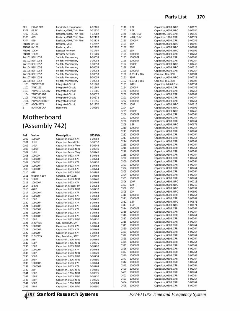
Parts List 170
Stanford Research Systems FS740 GPS Time and Frequency System
PC1 FS740 PCB Fabricated component 7-02461 R101 49.9K Resistor, 0603, Thin Film 4-02320 R102 20.0K Resistor, 0603, Thin Film 4-02282 R103 499 Resistor, 0603, Thin Film 4-02128 R104 499 Resistor, 0603, Thin Film 4-02128 RN101 8X100 Resistor, Misc. 4-02497 RN102 8X100 Resistor, Misc. 4-02497 RN103 10KX4 Resistor network 4-01789 RN104 10KX4 Resistor network 4-01789 SW101 B3F-1052 Switch, Momentary 2-00053 SW102 B3F-1052 Switch, Momentary 2-00053 SW103 B3F-1052 Switch, Momentary 2-00053 SW104 B3F-1052 Switch, Momentary 2-00053 SW105 B3F-1052 Switch, Momentary 2-00053 SW106 B3F-1052 Switch, Momentary 2-00053 SW107 B3F-1052 Switch, Momentary 2-00053 SW108 B3F-1052 Switch, Momentary 2-00053 U101 74LVC2G04 Integrated Circuit 3-01968 U102 74HC165 Integrated Circuit 3-01969 U103 74LVC1G125DBV Integrated Circuit 3-01886 U104 74HC595ADT Integrated Circuit 3-00672 U105 74HC595ADT Integrated Circuit 3-00672 U106 74LVC2G08DCT Integrated Circuit 3-01656 U107 ADCMP371 Integrated Circuit 3-01970 Z BUTTON CAP Hardware 0-00996
Motherboard (Assembly 742) Ref Value Description SRS P/N C100 10000P Capacitor, 0603, X7R 5-00752 C101 .01U Capacitor, Metal Film 5-00052 C102 1.0U Capacitor, Mylar/Poly 5-00245 C103 1000P Capacitor, 0603, NPO 5-00740 C104 1.0U Capacitor, Mylar/Poly 5-00245 C105 10000P Capacitor, 0603, X7R 5-00752 C106 100000P Capacitor, 0603, X7R 5-00764 C107 10000P Capacitor, 0603, X7R 5-00752 C108 100000P Capacitor, 0603, X7R 5-00764 C109 100000P Capacitor, 0603, X7R 5-00764 C110 47P Capacitor, 0603, NPO 5-00708 C111 0.01UF / 16V Ceramic, 16V, X5R 5-00604 C112 1000P Capacitor, 0603, NPO 5-00740 C113 100000P Capacitor, 0603, X7R 5-00764 C114 .047U Capacitor, Metal Film 5-00054 C115 470P Capacitor, 0603, NPO 5-00732 C117 100000P Capacitor, 0603, X7R 5-00764 C118 100000P Capacitor, 0603, X7R 5-00764 C119 150P Capacitor, 0603, NPO 5-00720 C120 100000P Capacitor, 0603, X7R 5-00764 C121 100000P Capacitor, 0603, X7R 5-00764 C122 100000P Capacitor, 0603, X7R 5-00764 C123 100000P Capacitor, 0603, X7R 5-00764 C124 100000P Capacitor, 0603, X7R 5-00764 C125 150P Capacitor, 0603, NPO 5-00720 C126 2.2U/T35 Cap, Tantalum, SMT 5-00318 C127 100000P Capacitor, 0603, X7R 5-00764 C128 100000P Capacitor, 0603, X7R 5-00764 C129 100000P Capacitor, 0603, X7R 5-00764 C130 2.2U/T35 Cap, Tantalum, SMT 5-00318 C131 33P Capacitor, 1206, NPO 5-00369 C132 100P Capacitor, 1206, NPO 5-00375 C133 150P Capacitor, 0603, NPO 5-00720 C134 100000P Capacitor, 0603, X7R 5-00764 C135 150P Capacitor, 0603, NPO 5-00720 C136 560P Capacitor, 0603, NPO 5-00734 C137 270P Capacitor, 1206, NPO 5-00380 C138 100000P Capacitor, 0603, X7R 5-00764 C139 100000P Capacitor, 0603, X7R 5-00764 C140 33P Capacitor, 1206, NPO 5-00369 C141 100P Capacitor, 1206, NPO 5-00375 C142 150P Capacitor, 0603, NPO 5-00720 C143 150P Capacitor, 0603, NPO 5-00720 C144 560P Capacitor, 1206, NPO 5-00384 C145 270P Capacitor, 1206, NPO 5-00380
C146 1.8P Capacitor, 0603, NPO 5-00673 C147 5.6P Capacitor, 0603, NPO 5-00684 C148 .47U / 16V Capacitor, 1206, X7R 5-00527 C149 .47U / 16V Capacitor, 1206, X7R 5-00527 C150 10000P Capacitor, 0603, X7R 5-00752 C151 18P Capacitor, 0603, NPO 5-00698 C152 27P Capacitor, 0603, NPO 5-00702 C153 15P Capacitor, 0603, NPO 5-00696 C154 100000P Capacitor, 0603, X7R 5-00764 C155 100000P Capacitor, 0603, X7R 5-00764 C156 100000P Capacitor, 0603, X7R 5-00764 C157 1000P Capacitor, 0603, NPO 5-00740 C158 100P Capacitor, 0603, NPO 5-00716 C159 100000P Capacitor, 0603, X7R 5-00764 C160 0.01UF / 16V Ceramic, 16V, X5R 5-00604 C161 330P Capacitor, 0603, NPO 5-00728 C162 0.01UF / 16V Ceramic, 16V, X5R 5-00604 C163 .047U Capacitor, Metal Film 5-00054 C164 10000P Capacitor, 0603, X7R 5-00752 C170 100000P Capacitor, 0603, X7R 5-00764 C200 100000P Capacitor, 0603, X7R 5-00764 C201 100000P Capacitor, 0603, X7R 5-00764 C202 100000P Capacitor, 0603, X7R 5-00764 C203 100P Capacitor, 0603, NPO 5-00716 C204 10P Capacitor, 0603, NPO 5-00692 C205 1000P Capacitor, 0603, NPO 5-00740 C206 100000P Capacitor, 0603, X7R 5-00764 C207 100000P Capacitor, 0603, X7R 5-00764 C208 100000P Capacitor, 0603, X7R 5-00764 C209 1.5P Capacitor, 0603, NPO 5-00671 C210 100000P Capacitor, 0603, X7R 5-00764 C211 100000P Capacitor, 0603, X7R 5-00764 C212 100000P Capacitor, 0603, X7R 5-00764 C213 100000P Capacitor, 0603, X7R 5-00764 C214 100000P Capacitor, 0603, X7R 5-00764 C215 100000P Capacitor, 0603, X7R 5-00764 C216 100000P Capacitor, 0603, X7R 5-00764 C218 100000P Capacitor, 0603, X7R 5-00764 C219 100000P Capacitor, 0603, X7R 5-00764 C220 100000P Capacitor, 0603, X7R 5-00764 C300 100000P Capacitor, 0603, X7R 5-00764 C301 100000P Capacitor, 0603, X7R 5-00764 C302 100000P Capacitor, 0603, X7R 5-00764 C303 100000P Capacitor, 0603, X7R 5-00764 C304 100000P Capacitor, 0603, X7R 5-00764 C305 100000P Capacitor, 0603, X7R 5-00764 C306 100P Capacitor, 0603, NPO 5-00716 C307 100P Capacitor, 0603, NPO 5-00716 C308 10P Capacitor, 0603, NPO 5-00692 C309 10P Capacitor, 0603, NPO 5-00692 C310 100000P Capacitor, 0603, X7R 5-00764 C311 100000P Capacitor, 0603, X7R 5-00764 C312 1.5P Capacitor, 0603, NPO 5-00671 C313 1.5P Capacitor, 0603, NPO 5-00671 C314 100000P Capacitor, 0603, X7R 5-00764 C315 100000P Capacitor, 0603, X7R 5-00764 C316 100000P Capacitor, 0603, X7R 5-00764 C317 100000P Capacitor, 0603, X7R 5-00764 C318 100000P Capacitor, 0603, X7R 5-00764 C319 100000P Capacitor, 0603, X7R 5-00764 C320 100000P Capacitor, 0603, X7R 5-00764 C321 100000P Capacitor, 0603, X7R 5-00764 C322 100000P Capacitor, 0603, X7R 5-00764 C323 100000P Capacitor, 0603, X7R 5-00764 C324 100000P Capacitor, 0603, X7R 5-00764 C325 100000P Capacitor, 0603, X7R 5-00764 C326 100000P Capacitor, 0603, X7R 5-00764 C327 100000P Capacitor, 0603, X7R 5-00764 C340 100000P Capacitor, 0603, X7R 5-00764 C341 100000P Capacitor, 0603, X7R 5-00764 C342 100000P Capacitor, 0603, X7R 5-00764 C343 100000P Capacitor, 0603, X7R 5-00764 C400 100000P Capacitor, 0603, X7R 5-00764 C401 100000P Capacitor, 0603, X7R 5-00764 C402 100000P Capacitor, 0603, X7R 5-00764 C403 100000P Capacitor, 0603, X7R 5-00764 C404 100000P Capacitor, 0603, X7R 5-00764 C405 100000P Capacitor, 0603, X7R 5-00764
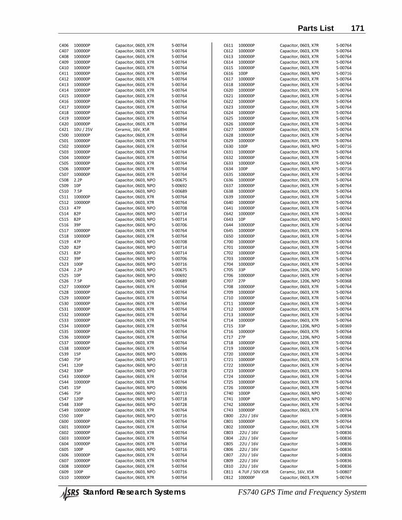
Parts List 171
Stanford Research Systems FS740 GPS Time and Frequency System
C406 100000P Capacitor, 0603, X7R 5-00764 C407 100000P Capacitor, 0603, X7R 5-00764 C408 100000P Capacitor, 0603, X7R 5-00764 C409 100000P Capacitor, 0603, X7R 5-00764 C410 100000P Capacitor, 0603, X7R 5-00764 C411 100000P Capacitor, 0603, X7R 5-00764 C412 100000P Capacitor, 0603, X7R 5-00764 C413 100000P Capacitor, 0603, X7R 5-00764 C414 100000P Capacitor, 0603, X7R 5-00764 C415 100000P Capacitor, 0603, X7R 5-00764 C416 100000P Capacitor, 0603, X7R 5-00764 C417 100000P Capacitor, 0603, X7R 5-00764 C418 100000P Capacitor, 0603, X7R 5-00764 C419 100000P Capacitor, 0603, X7R 5-00764 C420 100000P Capacitor, 0603, X7R 5-00764 C421 10U / 25V Ceramic, 16V, X5R 5-00894 C500 100000P Capacitor, 0603, X7R 5-00764 C501 100000P Capacitor, 0603, X7R 5-00764 C502 100000P Capacitor, 0603, X7R 5-00764 C503 100000P Capacitor, 0603, X7R 5-00764 C504 100000P Capacitor, 0603, X7R 5-00764 C505 100000P Capacitor, 0603, X7R 5-00764 C506 100000P Capacitor, 0603, X7R 5-00764 C507 100000P Capacitor, 0603, X7R 5-00764 C508 2.2P Capacitor, 0603, NPO 5-00675 C509 10P Capacitor, 0603, NPO 5-00692 C510 7.5P Capacitor, 0603, NPO 5-00689 C511 100000P Capacitor, 0603, X7R 5-00764 C512 100000P Capacitor, 0603, X7R 5-00764 C513 47P Capacitor, 0603, NPO 5-00708 C514 82P Capacitor, 0603, NPO 5-00714 C515 82P Capacitor, 0603, NPO 5-00714 C516 39P Capacitor, 0603, NPO 5-00706 C517 100000P Capacitor, 0603, X7R 5-00764 C518 100000P Capacitor, 0603, X7R 5-00764 C519 47P Capacitor, 0603, NPO 5-00708 C520 82P Capacitor, 0603, NPO 5-00714 C521 82P Capacitor, 0603, NPO 5-00714 C522 39P Capacitor, 0603, NPO 5-00706 C523 100P Capacitor, 0603, NPO 5-00716 C524 2.2P Capacitor, 0603, NPO 5-00675 C525 10P Capacitor, 0603, NPO 5-00692 C526 7.5P Capacitor, 0603, NPO 5-00689 C527 100000P Capacitor, 0603, X7R 5-00764 C528 100000P Capacitor, 0603, X7R 5-00764 C529 100000P Capacitor, 0603, X7R 5-00764 C530 100000P Capacitor, 0603, X7R 5-00764 C531 100000P Capacitor, 0603, X7R 5-00764 C532 100000P Capacitor, 0603, X7R 5-00764 C533 100000P Capacitor, 0603, X7R 5-00764 C534 100000P Capacitor, 0603, X7R 5-00764 C535 100000P Capacitor, 0603, X7R 5-00764 C536 100000P Capacitor, 0603, X7R 5-00764 C537 100000P Capacitor, 0603, X7R 5-00764 C538 100000P Capacitor, 0603, X7R 5-00764 C539 15P Capacitor, 0603, NPO 5-00696 C540 75P Capacitor, 0603, NPO 5-00713 C541 120P Capacitor, 0603, NPO 5-00718 C542 330P Capacitor, 0603, NPO 5-00728 C543 100000P Capacitor, 0603, X7R 5-00764 C544 100000P Capacitor, 0603, X7R 5-00764 C545 15P Capacitor, 0603, NPO 5-00696 C546 75P Capacitor, 0603, NPO 5-00713 C547 120P Capacitor, 0603, NPO 5-00718 C548 330P Capacitor, 0603, NPO 5-00728 C549 100000P Capacitor, 0603, X7R 5-00764 C550 100P Capacitor, 0603, NPO 5-00716 C600 100000P Capacitor, 0603, X7R 5-00764 C601 100000P Capacitor, 0603, X7R 5-00764 C602 100000P Capacitor, 0603, X7R 5-00764 C603 100000P Capacitor, 0603, X7R 5-00764 C604 100000P Capacitor, 0603, X7R 5-00764 C605 100P Capacitor, 0603, NPO 5-00716 C606 100000P Capacitor, 0603, X7R 5-00764 C607 100000P Capacitor, 0603, X7R 5-00764 C608 100000P Capacitor, 0603, X7R 5-00764 C609 100P Capacitor, 0603, NPO 5-00716 C610 100000P Capacitor, 0603, X7R 5-00764
C611 100000P Capacitor, 0603, X7R 5-00764 C612 100000P Capacitor, 0603, X7R 5-00764 C613 100000P Capacitor, 0603, X7R 5-00764 C614 100000P Capacitor, 0603, X7R 5-00764 C615 100000P Capacitor, 0603, X7R 5-00764 C616 100P Capacitor, 0603, NPO 5-00716 C617 100000P Capacitor, 0603, X7R 5-00764 C618 100000P Capacitor, 0603, X7R 5-00764 C620 100000P Capacitor, 0603, X7R 5-00764 C621 100000P Capacitor, 0603, X7R 5-00764 C622 100000P Capacitor, 0603, X7R 5-00764 C623 100000P Capacitor, 0603, X7R 5-00764 C624 100000P Capacitor, 0603, X7R 5-00764 C625 100000P Capacitor, 0603, X7R 5-00764 C626 100000P Capacitor, 0603, X7R 5-00764 C627 100000P Capacitor, 0603, X7R 5-00764 C628 100000P Capacitor, 0603, X7R 5-00764 C629 100000P Capacitor, 0603, X7R 5-00764 C630 100P Capacitor, 0603, NPO 5-00716 C631 100000P Capacitor, 0603, X7R 5-00764 C632 100000P Capacitor, 0603, X7R 5-00764 C633 100000P Capacitor, 0603, X7R 5-00764 C634 100P Capacitor, 0603, NPO 5-00716 C635 100000P Capacitor, 0603, X7R 5-00764 C636 100000P Capacitor, 0603, X7R 5-00764 C637 100000P Capacitor, 0603, X7R 5-00764 C638 100000P Capacitor, 0603, X7R 5-00764 C639 100000P Capacitor, 0603, X7R 5-00764 C640 100000P Capacitor, 0603, X7R 5-00764 C641 100000P Capacitor, 0603, X7R 5-00764 C642 100000P Capacitor, 0603, X7R 5-00764 C643 10P Capacitor, 0603, NPO 5-00692 C644 100000P Capacitor, 0603, X7R 5-00764 C645 100000P Capacitor, 0603, X7R 5-00764 C650 100000P Capacitor, 0603, X7R 5-00764 C700 100000P Capacitor, 0603, X7R 5-00764 C701 100000P Capacitor, 0603, X7R 5-00764 C702 100000P Capacitor, 0603, X7R 5-00764 C703 100000P Capacitor, 0603, X7R 5-00764 C704 100000P Capacitor, 0603, X7R 5-00764 C705 33P Capacitor, 1206, NPO 5-00369 C706 100000P Capacitor, 0603, X7R 5-00764 C707 27P Capacitor, 1206, NPO 5-00368 C708 100000P Capacitor, 0603, X7R 5-00764 C709 100000P Capacitor, 0603, X7R 5-00764 C710 100000P Capacitor, 0603, X7R 5-00764 C711 100000P Capacitor, 0603, X7R 5-00764 C712 100000P Capacitor, 0603, X7R 5-00764 C713 100000P Capacitor, 0603, X7R 5-00764 C714 100000P Capacitor, 0603, X7R 5-00764 C715 33P Capacitor, 1206, NPO 5-00369 C716 100000P Capacitor, 0603, X7R 5-00764 C717 27P Capacitor, 1206, NPO 5-00368 C718 100000P Capacitor, 0603, X7R 5-00764 C719 100000P Capacitor, 0603, X7R 5-00764 C720 100000P Capacitor, 0603, X7R 5-00764 C721 100000P Capacitor, 0603, X7R 5-00764 C722 100000P Capacitor, 0603, X7R 5-00764 C723 100000P Capacitor, 0603, X7R 5-00764 C724 100000P Capacitor, 0603, X7R 5-00764 C725 100000P Capacitor, 0603, X7R 5-00764 C726 100000P Capacitor, 0603, X7R 5-00764 C740 1000P Capacitor, 0603, NPO 5-00740 C741 1000P Capacitor, 0603, NPO 5-00740 C742 100000P Capacitor, 0603, X7R 5-00764 C743 100000P Capacitor, 0603, X7R 5-00764 C800 .22U / 16V Capacitor 5-00836 C801 100000P Capacitor, 0603, X7R 5-00764 C802 100000P Capacitor, 0603, X7R 5-00764 C803 .22U / 16V Capacitor 5-00836 C804 .22U / 16V Capacitor 5-00836 C805 .22U / 16V Capacitor 5-00836 C806 .22U / 16V Capacitor 5-00836 C807 .22U / 16V Capacitor 5-00836 C809 .22U / 16V Capacitor 5-00836 C810 .22U / 16V Capacitor 5-00836 C811 4.7UF / 50V X5R Ceramic, 16V, X5R 5-00807 C812 100000P Capacitor, 0603, X7R 5-00764
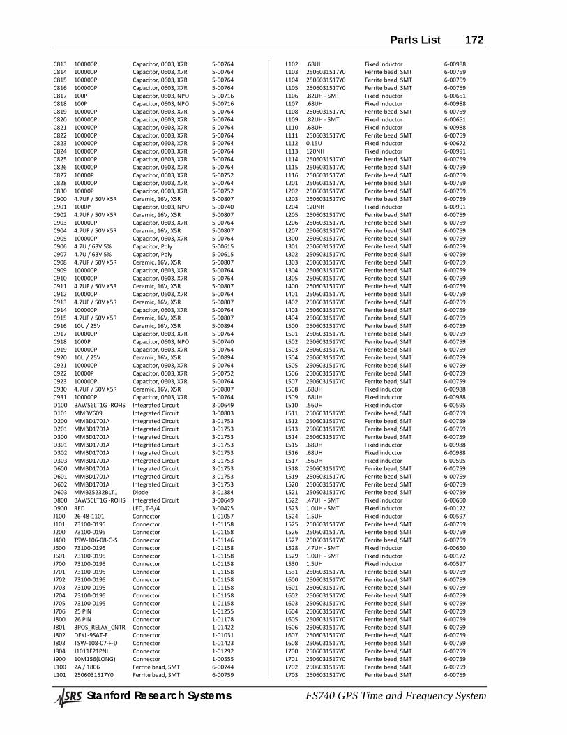
Parts List 172
Stanford Research Systems FS740 GPS Time and Frequency System
C813 100000P Capacitor, 0603, X7R 5-00764 C814 100000P Capacitor, 0603, X7R 5-00764 C815 100000P Capacitor, 0603, X7R 5-00764 C816 100000P Capacitor, 0603, X7R 5-00764 C817 100P Capacitor, 0603, NPO 5-00716 C818 100P Capacitor, 0603, NPO 5-00716 C819 100000P Capacitor, 0603, X7R 5-00764 C820 100000P Capacitor, 0603, X7R 5-00764 C821 100000P Capacitor, 0603, X7R 5-00764 C822 100000P Capacitor, 0603, X7R 5-00764 C823 100000P Capacitor, 0603, X7R 5-00764 C824 100000P Capacitor, 0603, X7R 5-00764 C825 100000P Capacitor, 0603, X7R 5-00764 C826 100000P Capacitor, 0603, X7R 5-00764 C827 10000P Capacitor, 0603, X7R 5-00752 C828 100000P Capacitor, 0603, X7R 5-00764 C830 10000P Capacitor, 0603, X7R 5-00752 C900 4.7UF / 50V X5R Ceramic, 16V, X5R 5-00807 C901 1000P Capacitor, 0603, NPO 5-00740 C902 4.7UF / 50V X5R Ceramic, 16V, X5R 5-00807 C903 100000P Capacitor, 0603, X7R 5-00764 C904 4.7UF / 50V X5R Ceramic, 16V, X5R 5-00807 C905 100000P Capacitor, 0603, X7R 5-00764 C906 4.7U / 63V 5% Capacitor, Poly 5-00615 C907 4.7U / 63V 5% Capacitor, Poly 5-00615 C908 4.7UF / 50V X5R Ceramic, 16V, X5R 5-00807 C909 100000P Capacitor, 0603, X7R 5-00764 C910 100000P Capacitor, 0603, X7R 5-00764 C911 4.7UF / 50V X5R Ceramic, 16V, X5R 5-00807 C912 100000P Capacitor, 0603, X7R 5-00764 C913 4.7UF / 50V X5R Ceramic, 16V, X5R 5-00807 C914 100000P Capacitor, 0603, X7R 5-00764 C915 4.7UF / 50V X5R Ceramic, 16V, X5R 5-00807 C916 10U / 25V Ceramic, 16V, X5R 5-00894 C917 100000P Capacitor, 0603, X7R 5-00764 C918 1000P Capacitor, 0603, NPO 5-00740 C919 100000P Capacitor, 0603, X7R 5-00764 C920 10U / 25V Ceramic, 16V, X5R 5-00894 C921 100000P Capacitor, 0603, X7R 5-00764 C922 10000P Capacitor, 0603, X7R 5-00752 C923 100000P Capacitor, 0603, X7R 5-00764 C930 4.7UF / 50V X5R Ceramic, 16V, X5R 5-00807 C931 100000P Capacitor, 0603, X7R 5-00764 D100 BAW56LT1G -ROHS Integrated Circuit 3-00649 D101 MMBV609 Integrated Circuit 3-00803 D200 MMBD1701A Integrated Circuit 3-01753 D201 MMBD1701A Integrated Circuit 3-01753 D300 MMBD1701A Integrated Circuit 3-01753 D301 MMBD1701A Integrated Circuit 3-01753 D302 MMBD1701A Integrated Circuit 3-01753 D303 MMBD1701A Integrated Circuit 3-01753 D600 MMBD1701A Integrated Circuit 3-01753 D601 MMBD1701A Integrated Circuit 3-01753 D602 MMBD1701A Integrated Circuit 3-01753 D603 MMBZ5232BLT1 Diode 3-01384 D800 BAW56LT1G -ROHS Integrated Circuit 3-00649 D900 RED LED, T-3/4 3-00425 J100 26-48-1101 Connector 1-01057 J101 73100-0195 Connector 1-01158 J200 73100-0195 Connector 1-01158 J400 TSW-106-08-G-S Connector 1-01146 J600 73100-0195 Connector 1-01158 J601 73100-0195 Connector 1-01158 J700 73100-0195 Connector 1-01158 J701 73100-0195 Connector 1-01158 J702 73100-0195 Connector 1-01158 J703 73100-0195 Connector 1-01158 J704 73100-0195 Connector 1-01158 J705 73100-0195 Connector 1-01158 J706 25 PIN Connector 1-01255 J800 26 PIN Connector 1-01178 J801 3POS_RELAY_CNTR Connector 1-01422 J802 DEKL-9SAT-E Connector 1-01031 J803 TSW-108-07-F-D Connector 1-01423 J804 J1011F21PNL Connector 1-01292 J900 10M156(LONG) Connector 1-00555 L100 2A / 1806 Ferrite bead, SMT 6-00744 L101 2506031517Y0 Ferrite bead, SMT 6-00759
L102 .68UH Fixed inductor 6-00988 L103 2506031517Y0 Ferrite bead, SMT 6-00759 L104 2506031517Y0 Ferrite bead, SMT 6-00759 L105 2506031517Y0 Ferrite bead, SMT 6-00759 L106 .82UH - SMT Fixed inductor 6-00651 L107 .68UH Fixed inductor 6-00988 L108 2506031517Y0 Ferrite bead, SMT 6-00759 L109 .82UH - SMT Fixed inductor 6-00651 L110 .68UH Fixed inductor 6-00988 L111 2506031517Y0 Ferrite bead, SMT 6-00759 L112 0.15U Fixed inductor 6-00672 L113 120NH Fixed inductor 6-00991 L114 2506031517Y0 Ferrite bead, SMT 6-00759 L115 2506031517Y0 Ferrite bead, SMT 6-00759 L116 2506031517Y0 Ferrite bead, SMT 6-00759 L201 2506031517Y0 Ferrite bead, SMT 6-00759 L202 2506031517Y0 Ferrite bead, SMT 6-00759 L203 2506031517Y0 Ferrite bead, SMT 6-00759 L204 120NH Fixed inductor 6-00991 L205 2506031517Y0 Ferrite bead, SMT 6-00759 L206 2506031517Y0 Ferrite bead, SMT 6-00759 L207 2506031517Y0 Ferrite bead, SMT 6-00759 L300 2506031517Y0 Ferrite bead, SMT 6-00759 L301 2506031517Y0 Ferrite bead, SMT 6-00759 L302 2506031517Y0 Ferrite bead, SMT 6-00759 L303 2506031517Y0 Ferrite bead, SMT 6-00759 L304 2506031517Y0 Ferrite bead, SMT 6-00759 L305 2506031517Y0 Ferrite bead, SMT 6-00759 L400 2506031517Y0 Ferrite bead, SMT 6-00759 L401 2506031517Y0 Ferrite bead, SMT 6-00759 L402 2506031517Y0 Ferrite bead, SMT 6-00759 L403 2506031517Y0 Ferrite bead, SMT 6-00759 L404 2506031517Y0 Ferrite bead, SMT 6-00759 L500 2506031517Y0 Ferrite bead, SMT 6-00759 L501 2506031517Y0 Ferrite bead, SMT 6-00759 L502 2506031517Y0 Ferrite bead, SMT 6-00759 L503 2506031517Y0 Ferrite bead, SMT 6-00759 L504 2506031517Y0 Ferrite bead, SMT 6-00759 L505 2506031517Y0 Ferrite bead, SMT 6-00759 L506 2506031517Y0 Ferrite bead, SMT 6-00759 L507 2506031517Y0 Ferrite bead, SMT 6-00759 L508 .68UH Fixed inductor 6-00988 L509 .68UH Fixed inductor 6-00988 L510 .56UH Fixed inductor 6-00595 L511 2506031517Y0 Ferrite bead, SMT 6-00759 L512 2506031517Y0 Ferrite bead, SMT 6-00759 L513 2506031517Y0 Ferrite bead, SMT 6-00759 L514 2506031517Y0 Ferrite bead, SMT 6-00759 L515 .68UH Fixed inductor 6-00988 L516 .68UH Fixed inductor 6-00988 L517 .56UH Fixed inductor 6-00595 L518 2506031517Y0 Ferrite bead, SMT 6-00759 L519 2506031517Y0 Ferrite bead, SMT 6-00759 L520 2506031517Y0 Ferrite bead, SMT 6-00759 L521 2506031517Y0 Ferrite bead, SMT 6-00759 L522 .47UH - SMT Fixed inductor 6-00650 L523 1.0UH - SMT Fixed inductor 6-00172 L524 1.5UH Fixed inductor 6-00597 L525 2506031517Y0 Ferrite bead, SMT 6-00759 L526 2506031517Y0 Ferrite bead, SMT 6-00759 L527 2506031517Y0 Ferrite bead, SMT 6-00759 L528 .47UH - SMT Fixed inductor 6-00650 L529 1.0UH - SMT Fixed inductor 6-00172 L530 1.5UH Fixed inductor 6-00597 L531 2506031517Y0 Ferrite bead, SMT 6-00759 L600 2506031517Y0 Ferrite bead, SMT 6-00759 L601 2506031517Y0 Ferrite bead, SMT 6-00759 L602 2506031517Y0 Ferrite bead, SMT 6-00759 L603 2506031517Y0 Ferrite bead, SMT 6-00759 L604 2506031517Y0 Ferrite bead, SMT 6-00759 L605 2506031517Y0 Ferrite bead, SMT 6-00759 L606 2506031517Y0 Ferrite bead, SMT 6-00759 L607 2506031517Y0 Ferrite bead, SMT 6-00759 L608 2506031517Y0 Ferrite bead, SMT 6-00759 L700 2506031517Y0 Ferrite bead, SMT 6-00759 L701 2506031517Y0 Ferrite bead, SMT 6-00759 L702 2506031517Y0 Ferrite bead, SMT 6-00759 L703 2506031517Y0 Ferrite bead, SMT 6-00759
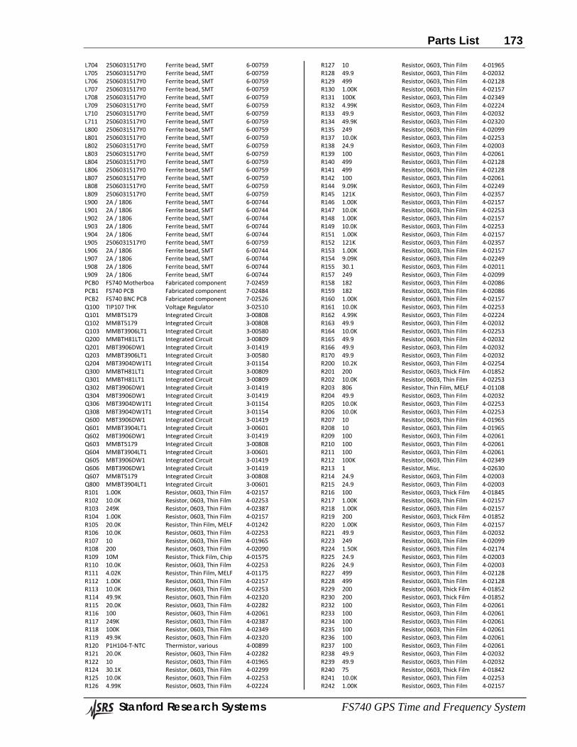
Parts List 173
Stanford Research Systems FS740 GPS Time and Frequency System
L704 2506031517Y0 Ferrite bead, SMT 6-00759 L705 2506031517Y0 Ferrite bead, SMT 6-00759 L706 2506031517Y0 Ferrite bead, SMT 6-00759 L707 2506031517Y0 Ferrite bead, SMT 6-00759 L708 2506031517Y0 Ferrite bead, SMT 6-00759 L709 2506031517Y0 Ferrite bead, SMT 6-00759 L710 2506031517Y0 Ferrite bead, SMT 6-00759 L711 2506031517Y0 Ferrite bead, SMT 6-00759 L800 2506031517Y0 Ferrite bead, SMT 6-00759 L801 2506031517Y0 Ferrite bead, SMT 6-00759 L802 2506031517Y0 Ferrite bead, SMT 6-00759 L803 2506031517Y0 Ferrite bead, SMT 6-00759 L804 2506031517Y0 Ferrite bead, SMT 6-00759 L806 2506031517Y0 Ferrite bead, SMT 6-00759 L807 2506031517Y0 Ferrite bead, SMT 6-00759 L808 2506031517Y0 Ferrite bead, SMT 6-00759 L809 2506031517Y0 Ferrite bead, SMT 6-00759 L900 2A / 1806 Ferrite bead, SMT 6-00744 L901 2A / 1806 Ferrite bead, SMT 6-00744 L902 2A / 1806 Ferrite bead, SMT 6-00744 L903 2A / 1806 Ferrite bead, SMT 6-00744 L904 2A / 1806 Ferrite bead, SMT 6-00744 L905 2506031517Y0 Ferrite bead, SMT 6-00759 L906 2A / 1806 Ferrite bead, SMT 6-00744 L907 2A / 1806 Ferrite bead, SMT 6-00744 L908 2A / 1806 Ferrite bead, SMT 6-00744 L909 2A / 1806 Ferrite bead, SMT 6-00744 PCB0 FS740 Motherboa Fabricated component 7-02459 PCB1 FS740 PCB Fabricated component 7-02484 PCB2 FS740 BNC PCB Fabricated component 7-02526 Q100 TIP107 THK Voltage Regulator 3-02510 Q101 MMBT5179 Integrated Circuit 3-00808 Q102 MMBT5179 Integrated Circuit 3-00808 Q103 MMBT3906LT1 Integrated Circuit 3-00580 Q200 MMBTH81LT1 Integrated Circuit 3-00809 Q201 MBT3906DW1 Integrated Circuit 3-01419 Q203 MMBT3906LT1 Integrated Circuit 3-00580 Q204 MBT3904DW1T1 Integrated Circuit 3-01154 Q300 MMBTH81LT1 Integrated Circuit 3-00809 Q301 MMBTH81LT1 Integrated Circuit 3-00809 Q302 MBT3906DW1 Integrated Circuit 3-01419 Q304 MBT3906DW1 Integrated Circuit 3-01419 Q306 MBT3904DW1T1 Integrated Circuit 3-01154 Q308 MBT3904DW1T1 Integrated Circuit 3-01154 Q600 MBT3906DW1 Integrated Circuit 3-01419 Q601 MMBT3904LT1 Integrated Circuit 3-00601 Q602 MBT3906DW1 Integrated Circuit 3-01419 Q603 MMBT5179 Integrated Circuit 3-00808 Q604 MMBT3904LT1 Integrated Circuit 3-00601 Q605 MBT3906DW1 Integrated Circuit 3-01419 Q606 MBT3906DW1 Integrated Circuit 3-01419 Q607 MMBT5179 Integrated Circuit 3-00808 Q800 MMBT3904LT1 Integrated Circuit 3-00601 R101 1.00K Resistor, 0603, Thin Film 4-02157 R102 10.0K Resistor, 0603, Thin Film 4-02253 R103 249K Resistor, 0603, Thin Film 4-02387 R104 1.00K Resistor, 0603, Thin Film 4-02157 R105 20.0K Resistor, Thin Film, MELF 4-01242 R106 10.0K Resistor, 0603, Thin Film 4-02253 R107 10 Resistor, 0603, Thin Film 4-01965 R108 200 Resistor, 0603, Thin Film 4-02090 R109 10M Resistor, Thick Film, Chip 4-01575 R110 10.0K Resistor, 0603, Thin Film 4-02253 R111 4.02K Resistor, Thin Film, MELF 4-01175 R112 1.00K Resistor, 0603, Thin Film 4-02157 R113 10.0K Resistor, 0603, Thin Film 4-02253 R114 49.9K Resistor, 0603, Thin Film 4-02320 R115 20.0K Resistor, 0603, Thin Film 4-02282 R116 100 Resistor, 0603, Thin Film 4-02061 R117 249K Resistor, 0603, Thin Film 4-02387 R118 100K Resistor, 0603, Thin Film 4-02349 R119 49.9K Resistor, 0603, Thin Film 4-02320 R120 P1H104-T-NTC Thermistor, various 4-00899 R121 20.0K Resistor, 0603, Thin Film 4-02282 R122 10 Resistor, 0603, Thin Film 4-01965 R124 30.1K Resistor, 0603, Thin Film 4-02299 R125 10.0K Resistor, 0603, Thin Film 4-02253 R126 4.99K Resistor, 0603, Thin Film 4-02224
R127 10 Resistor, 0603, Thin Film 4-01965 R128 49.9 Resistor, 0603, Thin Film 4-02032 R129 499 Resistor, 0603, Thin Film 4-02128 R130 1.00K Resistor, 0603, Thin Film 4-02157 R131 100K Resistor, 0603, Thin Film 4-02349 R132 4.99K Resistor, 0603, Thin Film 4-02224 R133 49.9 Resistor, 0603, Thin Film 4-02032 R134 49.9K Resistor, 0603, Thin Film 4-02320 R135 249 Resistor, 0603, Thin Film 4-02099 R137 10.0K Resistor, 0603, Thin Film 4-02253 R138 24.9 Resistor, 0603, Thin Film 4-02003 R139 100 Resistor, 0603, Thin Film 4-02061 R140 499 Resistor, 0603, Thin Film 4-02128 R141 499 Resistor, 0603, Thin Film 4-02128 R142 100 Resistor, 0603, Thin Film 4-02061 R144 9.09K Resistor, 0603, Thin Film 4-02249 R145 121K Resistor, 0603, Thin Film 4-02357 R146 1.00K Resistor, 0603, Thin Film 4-02157 R147 10.0K Resistor, 0603, Thin Film 4-02253 R148 1.00K Resistor, 0603, Thin Film 4-02157 R149 10.0K Resistor, 0603, Thin Film 4-02253 R151 1.00K Resistor, 0603, Thin Film 4-02157 R152 121K Resistor, 0603, Thin Film 4-02357 R153 1.00K Resistor, 0603, Thin Film 4-02157 R154 9.09K Resistor, 0603, Thin Film 4-02249 R155 30.1 Resistor, 0603, Thin Film 4-02011 R157 249 Resistor, 0603, Thin Film 4-02099 R158 182 Resistor, 0603, Thin Film 4-02086 R159 182 Resistor, 0603, Thin Film 4-02086 R160 1.00K Resistor, 0603, Thin Film 4-02157 R161 10.0K Resistor, 0603, Thin Film 4-02253 R162 4.99K Resistor, 0603, Thin Film 4-02224 R163 49.9 Resistor, 0603, Thin Film 4-02032 R164 10.0K Resistor, 0603, Thin Film 4-02253 R165 49.9 Resistor, 0603, Thin Film 4-02032 R166 49.9 Resistor, 0603, Thin Film 4-02032 R170 49.9 Resistor, 0603, Thin Film 4-02032 R200 10.2K Resistor, 0603, Thin Film 4-02254 R201 200 Resistor, 0603, Thick Film 4-01852 R202 10.0K Resistor, 0603, Thin Film 4-02253 R203 806 Resistor, Thin Film, MELF 4-01108 R204 49.9 Resistor, 0603, Thin Film 4-02032 R205 10.0K Resistor, 0603, Thin Film 4-02253 R206 10.0K Resistor, 0603, Thin Film 4-02253 R207 10 Resistor, 0603, Thin Film 4-01965 R208 10 Resistor, 0603, Thin Film 4-01965 R209 100 Resistor, 0603, Thin Film 4-02061 R210 100 Resistor, 0603, Thin Film 4-02061 R211 100 Resistor, 0603, Thin Film 4-02061 R212 100K Resistor, 0603, Thin Film 4-02349 R213 1 Resistor, Misc. 4-02630 R214 24.9 Resistor, 0603, Thin Film 4-02003 R215 24.9 Resistor, 0603, Thin Film 4-02003 R216 100 Resistor, 0603, Thick Film 4-01845 R217 1.00K Resistor, 0603, Thin Film 4-02157 R218 1.00K Resistor, 0603, Thin Film 4-02157 R219 200 Resistor, 0603, Thick Film 4-01852 R220 1.00K Resistor, 0603, Thin Film 4-02157 R221 49.9 Resistor, 0603, Thin Film 4-02032 R223 249 Resistor, 0603, Thin Film 4-02099 R224 1.50K Resistor, 0603, Thin Film 4-02174 R225 24.9 Resistor, 0603, Thin Film 4-02003 R226 24.9 Resistor, 0603, Thin Film 4-02003 R227 499 Resistor, 0603, Thin Film 4-02128 R228 499 Resistor, 0603, Thin Film 4-02128 R229 200 Resistor, 0603, Thick Film 4-01852 R230 200 Resistor, 0603, Thick Film 4-01852 R232 100 Resistor, 0603, Thin Film 4-02061 R233 100 Resistor, 0603, Thin Film 4-02061 R234 100 Resistor, 0603, Thin Film 4-02061 R235 100 Resistor, 0603, Thin Film 4-02061 R236 100 Resistor, 0603, Thin Film 4-02061 R237 100 Resistor, 0603, Thin Film 4-02061 R238 49.9 Resistor, 0603, Thin Film 4-02032 R239 49.9 Resistor, 0603, Thin Film 4-02032 R240 75 Resistor, 0603, Thick Film 4-01842 R241 10.0K Resistor, 0603, Thin Film 4-02253 R242 1.00K Resistor, 0603, Thin Film 4-02157
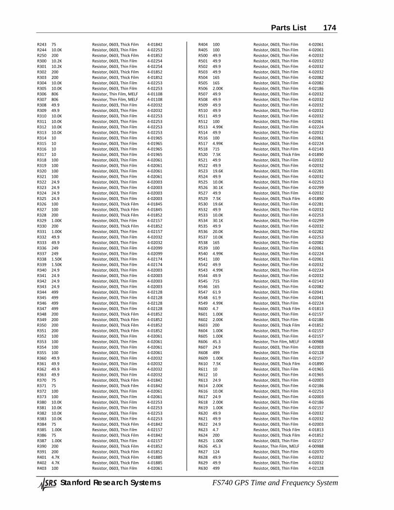
Parts List 174
Stanford Research Systems FS740 GPS Time and Frequency System
R243 75 Resistor, 0603, Thick Film 4-01842 R244 10.0K Resistor, 0603, Thin Film 4-02253 R250 200 Resistor, 0603, Thick Film 4-01852 R300 10.2K Resistor, 0603, Thin Film 4-02254 R301 10.2K Resistor, 0603, Thin Film 4-02254 R302 200 Resistor, 0603, Thick Film 4-01852 R303 200 Resistor, 0603, Thick Film 4-01852 R304 10.0K Resistor, 0603, Thin Film 4-02253 R305 10.0K Resistor, 0603, Thin Film 4-02253 R306 806 Resistor, Thin Film, MELF 4-01108 R307 806 Resistor, Thin Film, MELF 4-01108 R308 49.9 Resistor, 0603, Thin Film 4-02032 R309 49.9 Resistor, 0603, Thin Film 4-02032 R310 10.0K Resistor, 0603, Thin Film 4-02253 R311 10.0K Resistor, 0603, Thin Film 4-02253 R312 10.0K Resistor, 0603, Thin Film 4-02253 R313 10.0K Resistor, 0603, Thin Film 4-02253 R314 10 Resistor, 0603, Thin Film 4-01965 R315 10 Resistor, 0603, Thin Film 4-01965 R316 10 Resistor, 0603, Thin Film 4-01965 R317 10 Resistor, 0603, Thin Film 4-01965 R318 100 Resistor, 0603, Thin Film 4-02061 R319 100 Resistor, 0603, Thin Film 4-02061 R320 100 Resistor, 0603, Thin Film 4-02061 R321 100 Resistor, 0603, Thin Film 4-02061 R322 24.9 Resistor, 0603, Thin Film 4-02003 R323 24.9 Resistor, 0603, Thin Film 4-02003 R324 24.9 Resistor, 0603, Thin Film 4-02003 R325 24.9 Resistor, 0603, Thin Film 4-02003 R326 100 Resistor, 0603, Thick Film 4-01845 R327 100 Resistor, 0603, Thick Film 4-01845 R328 200 Resistor, 0603, Thick Film 4-01852 R329 1.00K Resistor, 0603, Thin Film 4-02157 R330 200 Resistor, 0603, Thick Film 4-01852 R331 1.00K Resistor, 0603, Thin Film 4-02157 R332 49.9 Resistor, 0603, Thin Film 4-02032 R333 49.9 Resistor, 0603, Thin Film 4-02032 R336 249 Resistor, 0603, Thin Film 4-02099 R337 249 Resistor, 0603, Thin Film 4-02099 R338 1.50K Resistor, 0603, Thin Film 4-02174 R339 1.50K Resistor, 0603, Thin Film 4-02174 R340 24.9 Resistor, 0603, Thin Film 4-02003 R341 24.9 Resistor, 0603, Thin Film 4-02003 R342 24.9 Resistor, 0603, Thin Film 4-02003 R343 24.9 Resistor, 0603, Thin Film 4-02003 R344 499 Resistor, 0603, Thin Film 4-02128 R345 499 Resistor, 0603, Thin Film 4-02128 R346 499 Resistor, 0603, Thin Film 4-02128 R347 499 Resistor, 0603, Thin Film 4-02128 R348 200 Resistor, 0603, Thick Film 4-01852 R349 200 Resistor, 0603, Thick Film 4-01852 R350 200 Resistor, 0603, Thick Film 4-01852 R351 200 Resistor, 0603, Thick Film 4-01852 R352 100 Resistor, 0603, Thin Film 4-02061 R353 100 Resistor, 0603, Thin Film 4-02061 R354 100 Resistor, 0603, Thin Film 4-02061 R355 100 Resistor, 0603, Thin Film 4-02061 R360 49.9 Resistor, 0603, Thin Film 4-02032 R361 49.9 Resistor, 0603, Thin Film 4-02032 R362 49.9 Resistor, 0603, Thin Film 4-02032 R363 49.9 Resistor, 0603, Thin Film 4-02032 R370 75 Resistor, 0603, Thick Film 4-01842 R371 75 Resistor, 0603, Thick Film 4-01842 R372 100 Resistor, 0603, Thin Film 4-02061 R373 100 Resistor, 0603, Thin Film 4-02061 R380 10.0K Resistor, 0603, Thin Film 4-02253 R381 10.0K Resistor, 0603, Thin Film 4-02253 R382 10.0K Resistor, 0603, Thin Film 4-02253 R383 10.0K Resistor, 0603, Thin Film 4-02253 R384 75 Resistor, 0603, Thick Film 4-01842 R385 1.00K Resistor, 0603, Thin Film 4-02157 R386 75 Resistor, 0603, Thick Film 4-01842 R387 1.00K Resistor, 0603, Thin Film 4-02157 R390 200 Resistor, 0603, Thick Film 4-01852 R391 200 Resistor, 0603, Thick Film 4-01852 R401 4.7K Resistor, 0603, Thick Film 4-01885 R402 4.7K Resistor, 0603, Thick Film 4-01885 R403 100 Resistor, 0603, Thin Film 4-02061
R404 100 Resistor, 0603, Thin Film 4-02061 R405 100 Resistor, 0603, Thin Film 4-02061 R500 49.9 Resistor, 0603, Thin Film 4-02032 R501 49.9 Resistor, 0603, Thin Film 4-02032 R502 49.9 Resistor, 0603, Thin Film 4-02032 R503 49.9 Resistor, 0603, Thin Film 4-02032 R504 165 Resistor, 0603, Thin Film 4-02082 R505 165 Resistor, 0603, Thin Film 4-02082 R506 2.00K Resistor, 0603, Thin Film 4-02186 R507 49.9 Resistor, 0603, Thin Film 4-02032 R508 49.9 Resistor, 0603, Thin Film 4-02032 R509 49.9 Resistor, 0603, Thin Film 4-02032 R510 49.9 Resistor, 0603, Thin Film 4-02032 R511 49.9 Resistor, 0603, Thin Film 4-02032 R512 100 Resistor, 0603, Thin Film 4-02061 R513 4.99K Resistor, 0603, Thin Film 4-02224 R514 49.9 Resistor, 0603, Thin Film 4-02032 R516 100 Resistor, 0603, Thin Film 4-02061 R517 4.99K Resistor, 0603, Thin Film 4-02224 R518 715 Resistor, 0603, Thin Film 4-02143 R520 7.5K Resistor, 0603, Thick Film 4-01890 R521 49.9 Resistor, 0603, Thin Film 4-02032 R522 49.9 Resistor, 0603, Thin Film 4-02032 R523 19.6K Resistor, 0603, Thin Film 4-02281 R524 49.9 Resistor, 0603, Thin Film 4-02032 R525 10.0K Resistor, 0603, Thin Film 4-02253 R526 30.1K Resistor, 0603, Thin Film 4-02299 R527 49.9 Resistor, 0603, Thin Film 4-02032 R529 7.5K Resistor, 0603, Thick Film 4-01890 R530 19.6K Resistor, 0603, Thin Film 4-02281 R532 49.9 Resistor, 0603, Thin Film 4-02032 R533 10.0K Resistor, 0603, Thin Film 4-02253 R534 30.1K Resistor, 0603, Thin Film 4-02299 R535 49.9 Resistor, 0603, Thin Film 4-02032 R536 20.0K Resistor, 0603, Thin Film 4-02282 R537 10.0K Resistor, 0603, Thin Film 4-02253 R538 165 Resistor, 0603, Thin Film 4-02082 R539 100 Resistor, 0603, Thin Film 4-02061 R540 4.99K Resistor, 0603, Thin Film 4-02224 R541 100 Resistor, 0603, Thin Film 4-02061 R542 49.9 Resistor, 0603, Thin Film 4-02032 R543 4.99K Resistor, 0603, Thin Film 4-02224 R544 49.9 Resistor, 0603, Thin Film 4-02032 R545 715 Resistor, 0603, Thin Film 4-02143 R546 165 Resistor, 0603, Thin Film 4-02082 R547 61.9 Resistor, 0603, Thin Film 4-02041 R548 61.9 Resistor, 0603, Thin Film 4-02041 R549 4.99K Resistor, 0603, Thin Film 4-02224 R600 4.7 Resistor, 0603, Thick Film 4-01813 R601 1.00K Resistor, 0603, Thin Film 4-02157 R602 2.00K Resistor, 0603, Thin Film 4-02186 R603 200 Resistor, 0603, Thick Film 4-01852 R604 1.00K Resistor, 0603, Thin Film 4-02157 R605 1.00K Resistor, 0603, Thin Film 4-02157 R606 45.3 Resistor, Thin Film, MELF 4-00988 R607 24.9 Resistor, 0603, Thin Film 4-02003 R608 499 Resistor, 0603, Thin Film 4-02128 R609 1.00K Resistor, 0603, Thin Film 4-02157 R610 7.5K Resistor, 0603, Thick Film 4-01890 R611 10 Resistor, 0603, Thin Film 4-01965 R612 10 Resistor, 0603, Thin Film 4-01965 R613 24.9 Resistor, 0603, Thin Film 4-02003 R614 2.00K Resistor, 0603, Thin Film 4-02186 R616 10.0K Resistor, 0603, Thin Film 4-02253 R617 24.9 Resistor, 0603, Thin Film 4-02003 R618 2.00K Resistor, 0603, Thin Film 4-02186 R619 1.00K Resistor, 0603, Thin Film 4-02157 R620 49.9 Resistor, 0603, Thin Film 4-02032 R621 49.9 Resistor, 0603, Thin Film 4-02032 R622 24.9 Resistor, 0603, Thin Film 4-02003 R623 4.7 Resistor, 0603, Thick Film 4-01813 R624 200 Resistor, 0603, Thick Film 4-01852 R625 1.00K Resistor, 0603, Thin Film 4-02157 R626 45.3 Resistor, Thin Film, MELF 4-00988 R627 124 Resistor, 0603, Thin Film 4-02070 R628 49.9 Resistor, 0603, Thin Film 4-02032 R629 49.9 Resistor, 0603, Thin Film 4-02032 R630 499 Resistor, 0603, Thin Film 4-02128
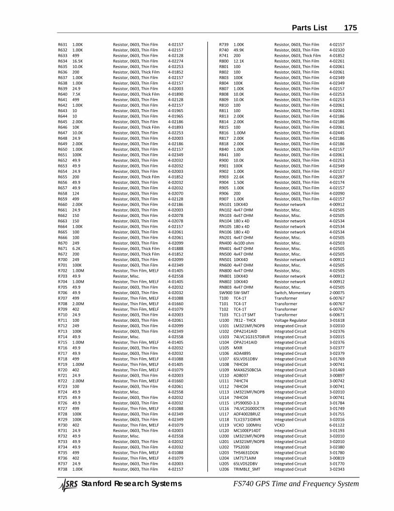
Parts List 175
Stanford Research Systems FS740 GPS Time and Frequency System
R631 1.00K Resistor, 0603, Thin Film 4-02157 R632 1.00K Resistor, 0603, Thin Film 4-02157 R633 499 Resistor, 0603, Thin Film 4-02128 R634 16.5K Resistor, 0603, Thin Film 4-02274 R635 10.0K Resistor, 0603, Thin Film 4-02253 R636 200 Resistor, 0603, Thick Film 4-01852 R637 1.00K Resistor, 0603, Thin Film 4-02157 R638 1.00K Resistor, 0603, Thin Film 4-02157 R639 24.9 Resistor, 0603, Thin Film 4-02003 R640 7.5K Resistor, 0603, Thick Film 4-01890 R641 499 Resistor, 0603, Thin Film 4-02128 R642 1.00K Resistor, 0603, Thin Film 4-02157 R643 10 Resistor, 0603, Thin Film 4-01965 R644 10 Resistor, 0603, Thin Film 4-01965 R645 2.00K Resistor, 0603, Thin Film 4-02186 R646 10K Resistor, 0603, Thick Film 4-01893 R647 10.0K Resistor, 0603, Thin Film 4-02253 R648 24.9 Resistor, 0603, Thin Film 4-02003 R649 2.00K Resistor, 0603, Thin Film 4-02186 R650 1.00K Resistor, 0603, Thin Film 4-02157 R651 100K Resistor, 0603, Thin Film 4-02349 R652 49.9 Resistor, 0603, Thin Film 4-02032 R653 49.9 Resistor, 0603, Thin Film 4-02032 R654 24.9 Resistor, 0603, Thin Film 4-02003 R655 200 Resistor, 0603, Thick Film 4-01852 R656 49.9 Resistor, 0603, Thin Film 4-02032 R657 49.9 Resistor, 0603, Thin Film 4-02032 R658 124 Resistor, 0603, Thin Film 4-02070 R659 499 Resistor, 0603, Thin Film 4-02128 R660 2.00K Resistor, 0603, Thin Film 4-02186 R661 24.9 Resistor, 0603, Thin Film 4-02003 R662 150 Resistor, 0603, Thin Film 4-02078 R663 150 Resistor, 0603, Thin Film 4-02078 R664 1.00K Resistor, 0603, Thin Film 4-02157 R665 100 Resistor, 0603, Thin Film 4-02061 R666 100 Resistor, 0603, Thin Film 4-02061 R670 249 Resistor, 0603, Thin Film 4-02099 R671 6.2K Resistor, 0603, Thick Film 4-01888 R672 200 Resistor, 0603, Thick Film 4-01852 R700 249 Resistor, 0603, Thin Film 4-02099 R701 100K Resistor, 0603, Thin Film 4-02349 R702 1.00M Resistor, Thin Film, MELF 4-01405 R703 49.9 Resistor, Misc. 4-02558 R704 1.00M Resistor, Thin Film, MELF 4-01405 R705 49.9 Resistor, 0603, Thin Film 4-02032 R706 49.9 Resistor, 0603, Thin Film 4-02032 R707 499 Resistor, Thin Film, MELF 4-01088 R708 2.00M Resistor, Thin Film, MELF 4-01660 R709 402 Resistor, Thin Film, MELF 4-01079 R710 24.9 Resistor, 0603, Thin Film 4-02003 R711 100 Resistor, 0603, Thin Film 4-02061 R712 249 Resistor, 0603, Thin Film 4-02099 R713 100K Resistor, 0603, Thin Film 4-02349 R714 49.9 Resistor, Misc. 4-02558 R715 1.00M Resistor, Thin Film, MELF 4-01405 R716 49.9 Resistor, 0603, Thin Film 4-02032 R717 49.9 Resistor, 0603, Thin Film 4-02032 R718 499 Resistor, Thin Film, MELF 4-01088 R719 1.00M Resistor, Thin Film, MELF 4-01405 R720 402 Resistor, Thin Film, MELF 4-01079 R721 24.9 Resistor, 0603, Thin Film 4-02003 R722 2.00M Resistor, Thin Film, MELF 4-01660 R723 100 Resistor, 0603, Thin Film 4-02061 R724 49.9 Resistor, Misc. 4-02558 R725 49.9 Resistor, 0603, Thin Film 4-02032 R726 49.9 Resistor, 0603, Thin Film 4-02032 R727 499 Resistor, Thin Film, MELF 4-01088 R728 100K Resistor, 0603, Thin Film 4-02349 R729 100K Resistor, 0603, Thin Film 4-02349 R730 402 Resistor, Thin Film, MELF 4-01079 R731 24.9 Resistor, 0603, Thin Film 4-02003 R732 49.9 Resistor, Misc. 4-02558 R733 49.9 Resistor, 0603, Thin Film 4-02032 R734 49.9 Resistor, 0603, Thin Film 4-02032 R735 499 Resistor, Thin Film, MELF 4-01088 R736 402 Resistor, Thin Film, MELF 4-01079 R737 24.9 Resistor, 0603, Thin Film 4-02003 R738 1.00K Resistor, 0603, Thin Film 4-02157
R739 1.00K Resistor, 0603, Thin Film 4-02157 R740 49.9K Resistor, 0603, Thin Film 4-02320 R741 200 Resistor, 0603, Thick Film 4-01852 R800 12.1K Resistor, 0603, Thin Film 4-02261 R801 100 Resistor, 0603, Thin Film 4-02061 R802 100 Resistor, 0603, Thin Film 4-02061 R803 100K Resistor, 0603, Thin Film 4-02349 R804 100K Resistor, 0603, Thin Film 4-02349 R807 1.00K Resistor, 0603, Thin Film 4-02157 R808 10.0K Resistor, 0603, Thin Film 4-02253 R809 10.0K Resistor, 0603, Thin Film 4-02253 R810 100 Resistor, 0603, Thin Film 4-02061 R811 100 Resistor, 0603, Thin Film 4-02061 R813 2.00K Resistor, 0603, Thin Film 4-02186 R814 2.00K Resistor, 0603, Thin Film 4-02186 R815 100 Resistor, 0603, Thin Film 4-02061 R816 1.00M Resistor, 0603, Thin Film 4-02445 R817 2.00K Resistor, 0603, Thin Film 4-02186 R818 2.00K Resistor, 0603, Thin Film 4-02186 R840 1.00K Resistor, 0603, Thin Film 4-02157 R841 100 Resistor, 0603, Thin Film 4-02061 R900 10.0K Resistor, 0603, Thin Film 4-02253 R901 100K Resistor, 0603, Thin Film 4-02349 R902 1.00K Resistor, 0603, Thin Film 4-02157 R903 22.6K Resistor, 0603, Thin Film 4-02287 R904 1.50K Resistor, 0603, Thin Film 4-02174 R905 1.00K Resistor, 0603, Thin Film 4-02157 R906 200 Resistor, 0603, Thin Film 4-02090 R907 1.00K Resistor, 0603, Thin Film 4-02157 RN101 10KX4D Resistor network 4-00912 RN102 4x47 OHM Resistor, Misc. 4-02505 RN103 4x47 OHM Resistor, Misc. 4-02505 RN104 180 x 4D Resistor network 4-02534 RN105 180 x 4D Resistor network 4-02534 RN106 180 x 4D Resistor network 4-02534 RN201 4x47 OHM Resistor, Misc. 4-02505 RN400 4x100 ohm Resistor, Misc. 4-02503 RN401 4x47 OHM Resistor, Misc. 4-02505 RN500 4x47 OHM Resistor, Misc. 4-02505 RN501 10KX4D Resistor network 4-00912 RN600 4x47 OHM Resistor, Misc. 4-02505 RN800 4x47 OHM Resistor, Misc. 4-02505 RN801 10KX4D Resistor network 4-00912 RN802 10KX4D Resistor network 4-00912 RN803 4x47 OHM Resistor, Misc. 4-02505 SW900 SW-SMT Switch, Momentary 2-00075 T100 TC4-1T Transformer 6-00767 T101 TC4-1T Transformer 6-00767 T102 TC4-1T Transformer 6-00767 T103 TC1-1T SMT Transformer 6-00671 U100 7812 - THCK Voltage Regulator 3-01618 U101 LM321MF/NOPB Integrated Circuit 3-02010 U102 OPA2141AID Integrated Circuit 3-02376 U103 74LVC1G3157DBVR Integrated Circuit 3-02015 U104 OPA2141AID Integrated Circuit 3-02376 U105 MXR Integrated Circuit 3-02377 U106 ADA4895 Integrated Circuit 3-02379 U107 65LVDS1DBV Integrated Circuit 3-01769 U108 74HC04 Integrated Circuit 3-00741 U109 MAX6250BCSA Integrated Circuit 3-01469 U110 AD8037 Integrated Circuit 3-00897 U111 74HC74 Integrated Circuit 3-00742 U112 74HC04 Integrated Circuit 3-00741 U113 LM321MF/NOPB Integrated Circuit 3-02010 U114 74HC04 Integrated Circuit 3-00741 U115 LP5900SD-3.3 Integrated Circuit 3-01784 U116 74LVC2G00DCTR Integrated Circuit 3-01749 U117 ADF4002BRUZ Integrated Circuit 3-01755 U118 TLV2371IDBVR Integrated Circuit 3-02016 U119 VCXO 100MHz VCXO 6-01122 U120 MC100EP14DT Integrated Circuit 3-01193 U200 LM321MF/NOPB Integrated Circuit 3-02010 U201 LM321MF/NOPB Integrated Circuit 3-02010 U202 TPS2030 Integrated Circuit 3-02380 U203 THS4631DGN Integrated Circuit 3-01780 U204 LM7171AIM Integrated Circuit 3-00819 U205 65LVDS2DBV Integrated Circuit 3-01770 U206 TRIMBLE_SMT Integrated Circuit 3-02343
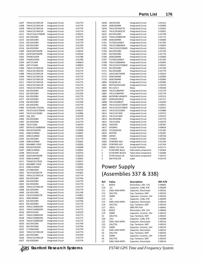
Parts List 176
Stanford Research Systems FS740 GPS Time and Frequency System
U207 74AUC1G74DCUR Integrated Circuit 3-01774 U208 74AUC1G74DCUR Integrated Circuit 3-01774 U209 74AUC1G74DCUR Integrated Circuit 3-01774 U210 74AUC1G74DCUR Integrated Circuit 3-01774 U211 74LVC1G3157DBVR Integrated Circuit 3-02015 U212 65LVDS2DBV Integrated Circuit 3-01770 U213 65LVDS1DBV Integrated Circuit 3-01769 U214 65LVDS2DBV Integrated Circuit 3-01770 U215 65LVDS1DBV Integrated Circuit 3-01769 U216 65LVDS2DBV Integrated Circuit 3-01770 U300 LM321MF/NOPB Integrated Circuit 3-02010 U301 LM321MF/NOPB Integrated Circuit 3-02010 U302 THS4631DGN Integrated Circuit 3-01780 U303 THS4631DGN Integrated Circuit 3-01780 U304 LM7171AIM Integrated Circuit 3-00819 U305 LM7171AIM Integrated Circuit 3-00819 U306 74AUC1G74DCUR Integrated Circuit 3-01774 U307 74AUC1G74DCUR Integrated Circuit 3-01774 U308 74AUC1G74DCUR Integrated Circuit 3-01774 U309 74AUC1G74DCUR Integrated Circuit 3-01774 U310 74AUC1G74DCUR Integrated Circuit 3-01774 U311 74AUC1G74DCUR Integrated Circuit 3-01774 U312 74AUC1G74DCUR Integrated Circuit 3-01774 U313 74AUC1G74DCUR Integrated Circuit 3-01774 U314 65LVDS2DBV Integrated Circuit 3-01770 U315 65LVDS1DBV Integrated Circuit 3-01769 U316 65LVDS2DBV Integrated Circuit 3-01770 U317 65LVDS2DBV Integrated Circuit 3-01770 U318 65LVDS1DBV Integrated Circuit 3-01769 U319 65LVDS2DBV Integrated Circuit 3-01770 U400 XC3S250E-4TQ144 Integrated Circuit 3-01783 U401 74LVC1G3157DBVR Integrated Circuit 3-02015 U402 74LVC1G125DBV Integrated Circuit 3-01886 U403 16b_ADC Integrated Circuit 3-02378 U404 65LVDS2DBV Integrated Circuit 3-01770 U405 65LVDS2DBV Integrated Circuit 3-01770 U406 74LVC1G04 Integrated Circuit 3-02070 U407 SN74LVC1G08DBVR Integrated Circuit 3-01203 U500 DAC5672AIPFB Integrated Circuit 3-02008 U501 AD8131ARMZ Integrated Circuit 3-02001 U502 AD8131ARMZ Integrated Circuit 3-02001 U503 65LVDS2DBV Integrated Circuit 3-01770 U504 AD8131ARMZ Integrated Circuit 3-02001 U505 ADA4860-1YRJZ Integrated Circuit 3-02003 U506 DAC5672AIPFB Integrated Circuit 3-02008 U507 AD8131ARMZ Integrated Circuit 3-02001 U508 OPA2141AID Integrated Circuit 3-02376 U509 LM321MF/NOPB Integrated Circuit 3-02010 U510 AD8131ARMZ Integrated Circuit 3-02001 U511 TS5A623157DGS Integrated Circuit 3-02017 U512 ADA4860-1YRJZ Integrated Circuit 3-02003 U513 AD8131ARMZ Integrated Circuit 3-02001 U600 LT1396CMS8 Integrated Circuit 3-01759 U601 74LVC3G34DCTR Integrated Circuit 3-01852 U602 74AUC1G74DCUR Integrated Circuit 3-01774 U603 65LVDS1DBV Integrated Circuit 3-01769 U604 65LVDS2DBV Integrated Circuit 3-01770 U605 65LVDS2DBV Integrated Circuit 3-01770 U606 74AUC1G74DCUR Integrated Circuit 3-01774 U608 65LVDS2DBV Integrated Circuit 3-01770 U609 65LVDS1DBV Integrated Circuit 3-01769 U610 74LVC3G34DCTR Integrated Circuit 3-01852 U611 AD8130ARM Integrated Circuit 3-02000 U612 65LVDS1DBV Integrated Circuit 3-01769 U613 65LVDS2DBV Integrated Circuit 3-01770 U614 74AUC1G86DCKR Integrated Circuit 3-01775 U615 74AUC1G08DCKR Integrated Circuit 3-01772 U616 OPA2141AID Integrated Circuit 3-02376 U617 74AUC1G86DCKR Integrated Circuit 3-01775 U618 74AUC1G08DCKR Integrated Circuit 3-01772 U619 74AUC1G08DCKR Integrated Circuit 3-01772 U620 65LVDS1DBV Integrated Circuit 3-01769 U621 65LVDS1DBV Integrated Circuit 3-01769 U622 LT1396CMS8 Integrated Circuit 3-01759 U623 74AUC1G74DCUR Integrated Circuit 3-01774 U624 65LVDS1DBV Integrated Circuit 3-01769 U626 74AUC1G74DCUR Integrated Circuit 3-01774 U627 65LVDS2DBV Integrated Circuit 3-01770
U628 LMV321M5 Integrated Circuit 3-01412 U629 AD8130ARM Integrated Circuit 3-02000 U630 74LVC3G34DCTR Integrated Circuit 3-01852 U631 74LVC3G34DCTR Integrated Circuit 3-01852 U632 65LVDS1DBV Integrated Circuit 3-01769 U633 74AUC1G08DCKR Integrated Circuit 3-01772 U700 AD8130ARM Integrated Circuit 3-02000 U701 TLV3501AIDBVT Integrated Circuit 3-01782 U702 74LVC1G86DBVR Integrated Circuit 3-01854 U703 74LVC1G3157DBVR Integrated Circuit 3-02015 U704 65LVDS1DBV Integrated Circuit 3-01769 U705 65LVDS2DBV Integrated Circuit 3-01770 U706 AD8130ARM Integrated Circuit 3-02000 U707 TLV3501AIDBVT Integrated Circuit 3-01782 U708 74LVC1G86DBVR Integrated Circuit 3-01854 U709 74LVC1G3157DBVR Integrated Circuit 3-02015 U710 65LVDS1DBV Integrated Circuit 3-01769 U711 65LVDS2DBV Integrated Circuit 3-01770 U712 LM321MF/NOPB Integrated Circuit 3-02010 U713 AD8130ARM Integrated Circuit 3-02000 U714 AD8130ARM Integrated Circuit 3-02000 U800 DS1816R-20 Integrated Circuit 3-02084 U801 MCF52235CAL60 Integrated Circuit 3-01676 U803 HS-212S-5 Relay 3-00196 U804 74LVC138APWT Integrated Circuit 3-01779 U805 74LVC138APWT Integrated Circuit 3-01779 U806 M25PE80-VMN6TP Integrated Circuit 3-02313 U807 ADM3202ARUZ Integrated Circuit 3-01757 U808 74LVC2G08DCT Integrated Circuit 3-01656 U809 74LVC1G3157DBVR Integrated Circuit 3-02015 U810 74LVC1G3157DBVR Integrated Circuit 3-02015 U811 74LVC1G125DBV Integrated Circuit 3-01886 U812 74LVC1G74DP Integrated Circuit 3-01973 U813 74LVC1G74DP Integrated Circuit 3-01973 U814 65LVDS2DBV Integrated Circuit 3-01770 U815 74LVC1G04 Integrated Circuit 3-02070 U816 74HC595 Integrated Circuit 3-00787 U817 OP284FS Integrated Circuit 3-00659 U818 LTC2620CGN Integrated Circuit 3-01185 U819 AD5760 Integrated Circuit 3-02381 U900 LM393 Integrated Circuit 3-00728 U901 LTC6655 Integrated Circuit 3-02382 U902 LP3878SD-ADJ Integrated Circuit 3-01764 U903 LP3878SD-ADJ Integrated Circuit 3-01764 Y101 20MHz 55C Xtal Crystal Oscillator 6-01171 Z FS740 BNC Block Fabricated component 7-02464 Z FS740 BNC BLOCK Fabricated component 7-02468 Z FS740 Heater Sh Fabricated component 7-02472 Z SIM-PCB S/N Label 9-01570
Power Supply (Assemblies 337 & 338) Ref Value Description SRS P/N C1 820UF Electrolytic, 50V, T/H 5-00844 C10 .1U Capacitor, 1206, X7R 5-00299 C11 330U HIGH RIPPL Capacitor, Electrolytic 5-00516 C12 10U/T35 Cap, Tantalum, SMT 5-00319 C13 1000P Capacitor, Ceramic, 1kV 5-00143 C14 .1U Capacitor, 1206, X7R 5-00299 C15 330U HIGH RIPPL Capacitor, Electrolytic 5-00516 C16 10U/T35 Cap, Tantalum, SMT 5-00319 C17 .001U SMD PPS Film 5-00442 C18 820UF Electrolytic, 50V, T/H 5-00844 C19 1000P Capacitor, Ceramic, 1kV 5-00143 C2 10U/T35 Cap, Tantalum, SMT 5-00319 C20 .01U Capacitor, 1206, X7R 5-00298 C21 330U HIGH RIPPL Capacitor, Electrolytic 5-00516 C22 10U/T35 Cap, Tantalum, SMT 5-00319 C23 1000P Capacitor, Ceramic, 1kV 5-00143 C3 330U HIGH RIPPL Capacitor, Electrolytic 5-00516 C4 10U/T35 Cap, Tantalum, SMT 5-00319 C5 1000P Capacitor, Ceramic, 1kV 5-00143 C6 10U/T35 Cap, Tantalum, SMT 5-00319 C7 330U HIGH RIPPL Capacitor, Electrolytic 5-00516
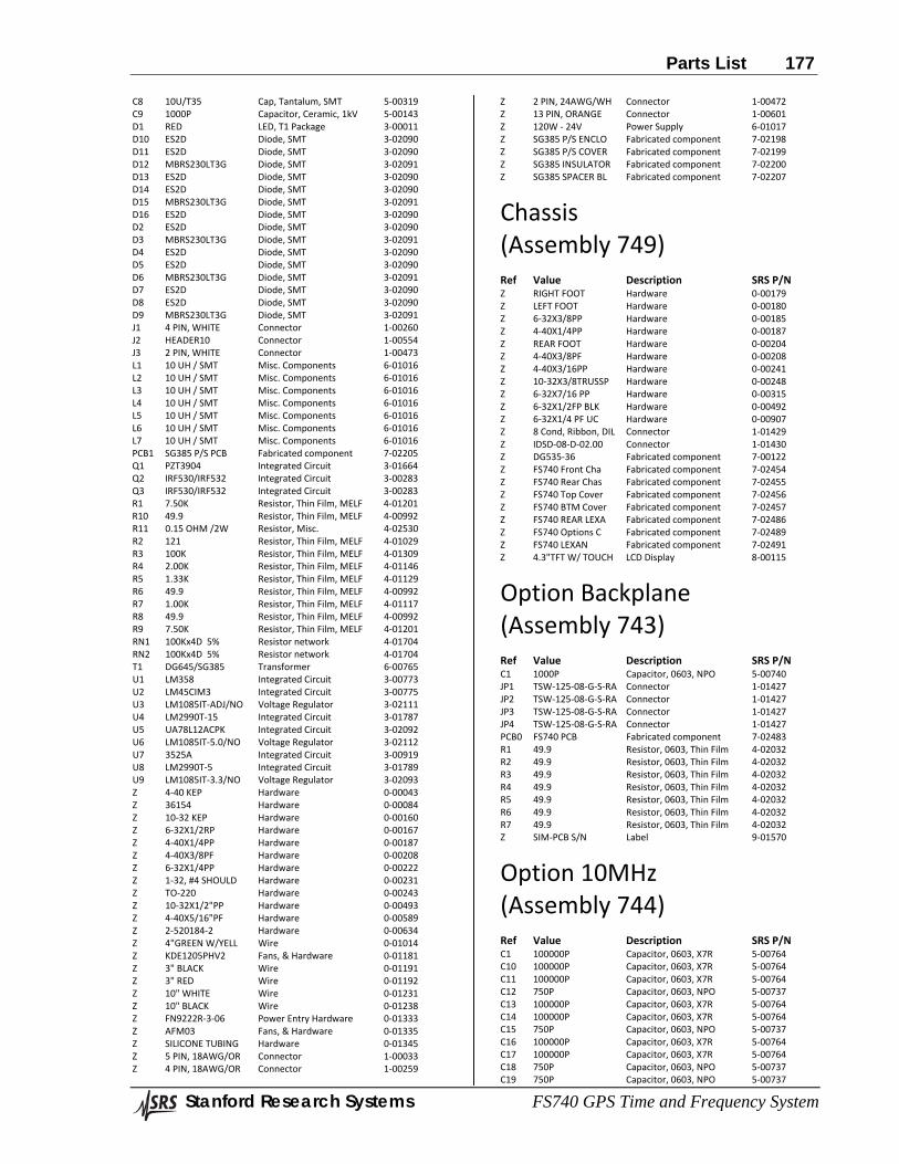
Parts List 177
Stanford Research Systems FS740 GPS Time and Frequency System
C8 10U/T35 Cap, Tantalum, SMT 5-00319 C9 1000P Capacitor, Ceramic, 1kV 5-00143 D1 RED LED, T1 Package 3-00011 D10 ES2D Diode, SMT 3-02090 D11 ES2D Diode, SMT 3-02090 D12 MBRS230LT3G Diode, SMT 3-02091 D13 ES2D Diode, SMT 3-02090 D14 ES2D Diode, SMT 3-02090 D15 MBRS230LT3G Diode, SMT 3-02091 D16 ES2D Diode, SMT 3-02090 D2 ES2D Diode, SMT 3-02090 D3 MBRS230LT3G Diode, SMT 3-02091 D4 ES2D Diode, SMT 3-02090 D5 ES2D Diode, SMT 3-02090 D6 MBRS230LT3G Diode, SMT 3-02091 D7 ES2D Diode, SMT 3-02090 D8 ES2D Diode, SMT 3-02090 D9 MBRS230LT3G Diode, SMT 3-02091 J1 4 PIN, WHITE Connector 1-00260 J2 HEADER10 Connector 1-00554 J3 2 PIN, WHITE Connector 1-00473 L1 10 UH / SMT Misc. Components 6-01016 L2 10 UH / SMT Misc. Components 6-01016 L3 10 UH / SMT Misc. Components 6-01016 L4 10 UH / SMT Misc. Components 6-01016 L5 10 UH / SMT Misc. Components 6-01016 L6 10 UH / SMT Misc. Components 6-01016 L7 10 UH / SMT Misc. Components 6-01016 PCB1 SG385 P/S PCB Fabricated component 7-02205 Q1 PZT3904 Integrated Circuit 3-01664 Q2 IRF530/IRF532 Integrated Circuit 3-00283 Q3 IRF530/IRF532 Integrated Circuit 3-00283 R1 7.50K Resistor, Thin Film, MELF 4-01201 R10 49.9 Resistor, Thin Film, MELF 4-00992 R11 0.15 OHM /2W Resistor, Misc. 4-02530 R2 121 Resistor, Thin Film, MELF 4-01029 R3 100K Resistor, Thin Film, MELF 4-01309 R4 2.00K Resistor, Thin Film, MELF 4-01146 R5 1.33K Resistor, Thin Film, MELF 4-01129 R6 49.9 Resistor, Thin Film, MELF 4-00992 R7 1.00K Resistor, Thin Film, MELF 4-01117 R8 49.9 Resistor, Thin Film, MELF 4-00992 R9 7.50K Resistor, Thin Film, MELF 4-01201 RN1 100Kx4D 5% Resistor network 4-01704 RN2 100Kx4D 5% Resistor network 4-01704 T1 DG645/SG385 Transformer 6-00765 U1 LM358 Integrated Circuit 3-00773 U2 LM45CIM3 Integrated Circuit 3-00775 U3 LM1085IT-ADJ/NO Voltage Regulator 3-02111 U4 LM2990T-15 Integrated Circuit 3-01787 U5 UA78L12ACPK Integrated Circuit 3-02092 U6 LM1085IT-5.0/NO Voltage Regulator 3-02112 U7 3525A Integrated Circuit 3-00919 U8 LM2990T-5 Integrated Circuit 3-01789 U9 LM1085IT-3.3/NO Voltage Regulator 3-02093 Z 4-40 KEP Hardware 0-00043 Z 36154 Hardware 0-00084 Z 10-32 KEP Hardware 0-00160 Z 6-32X1/2RP Hardware 0-00167 Z 4-40X1/4PP Hardware 0-00187 Z 4-40X3/8PF Hardware 0-00208 Z 6-32X1/4PP Hardware 0-00222 Z 1-32, #4 SHOULD Hardware 0-00231 Z TO-220 Hardware 0-00243 Z 10-32X1/2"PP Hardware 0-00493 Z 4-40X5/16"PF Hardware 0-00589 Z 2-520184-2 Hardware 0-00634 Z 4"GREEN W/YELL Wire 0-01014 Z KDE1205PHV2 Fans, & Hardware 0-01181 Z 3" BLACK Wire 0-01191 Z 3" RED Wire 0-01192 Z 10" WHITE Wire 0-01231 Z 10" BLACK Wire 0-01238 Z FN9222R-3-06 Power Entry Hardware 0-01333 Z AFM03 Fans, & Hardware 0-01335 Z SILICONE TUBING Hardware 0-01345 Z 5 PIN, 18AWG/OR Connector 1-00033 Z 4 PIN, 18AWG/OR Connector 1-00259
Z 2 PIN, 24AWG/WH Connector 1-00472 Z 13 PIN, ORANGE Connector 1-00601 Z 120W - 24V Power Supply 6-01017 Z SG385 P/S ENCLO Fabricated component 7-02198 Z SG385 P/S COVER Fabricated component 7-02199 Z SG385 INSULATOR Fabricated component 7-02200 Z SG385 SPACER BL Fabricated component 7-02207
Chassis (Assembly 749) Ref Value Description SRS P/N Z RIGHT FOOT Hardware 0-00179 Z LEFT FOOT Hardware 0-00180 Z 6-32X3/8PP Hardware 0-00185 Z 4-40X1/4PP Hardware 0-00187 Z REAR FOOT Hardware 0-00204 Z 4-40X3/8PF Hardware 0-00208 Z 4-40X3/16PP Hardware 0-00241 Z 10-32X3/8TRUSSP Hardware 0-00248 Z 6-32X7/16 PP Hardware 0-00315 Z 6-32X1/2FP BLK Hardware 0-00492 Z 6-32X1/4 PF UC Hardware 0-00907 Z 8 Cond, Ribbon, DIL Connector 1-01429 Z IDSD-08-D-02.00 Connector 1-01430 Z DG535-36 Fabricated component 7-00122 Z FS740 Front Cha Fabricated component 7-02454 Z FS740 Rear Chas Fabricated component 7-02455 Z FS740 Top Cover Fabricated component 7-02456 Z FS740 BTM Cover Fabricated component 7-02457 Z FS740 REAR LEXA Fabricated component 7-02486 Z FS740 Options C Fabricated component 7-02489 Z FS740 LEXAN Fabricated component 7-02491 Z 4.3"TFT W/ TOUCH LCD Display 8-00115
Option Backplane (Assembly 743) Ref Value Description SRS P/N C1 1000P Capacitor, 0603, NPO 5-00740 JP1 TSW-125-08-G-S-RA Connector 1-01427 JP2 TSW-125-08-G-S-RA Connector 1-01427 JP3 TSW-125-08-G-S-RA Connector 1-01427 JP4 TSW-125-08-G-S-RA Connector 1-01427 PCB0 FS740 PCB Fabricated component 7-02483 R1 49.9 Resistor, 0603, Thin Film 4-02032 R2 49.9 Resistor, 0603, Thin Film 4-02032 R3 49.9 Resistor, 0603, Thin Film 4-02032 R4 49.9 Resistor, 0603, Thin Film 4-02032 R5 49.9 Resistor, 0603, Thin Film 4-02032 R6 49.9 Resistor, 0603, Thin Film 4-02032 R7 49.9 Resistor, 0603, Thin Film 4-02032 Z SIM-PCB S/N Label 9-01570
Option 10MHz (Assembly 744) Ref Value Description SRS P/N C1 100000P Capacitor, 0603, X7R 5-00764 C10 100000P Capacitor, 0603, X7R 5-00764 C11 100000P Capacitor, 0603, X7R 5-00764 C12 750P Capacitor, 0603, NPO 5-00737 C13 100000P Capacitor, 0603, X7R 5-00764 C14 100000P Capacitor, 0603, X7R 5-00764 C15 750P Capacitor, 0603, NPO 5-00737 C16 100000P Capacitor, 0603, X7R 5-00764 C17 100000P Capacitor, 0603, X7R 5-00764 C18 750P Capacitor, 0603, NPO 5-00737 C19 750P Capacitor, 0603, NPO 5-00737
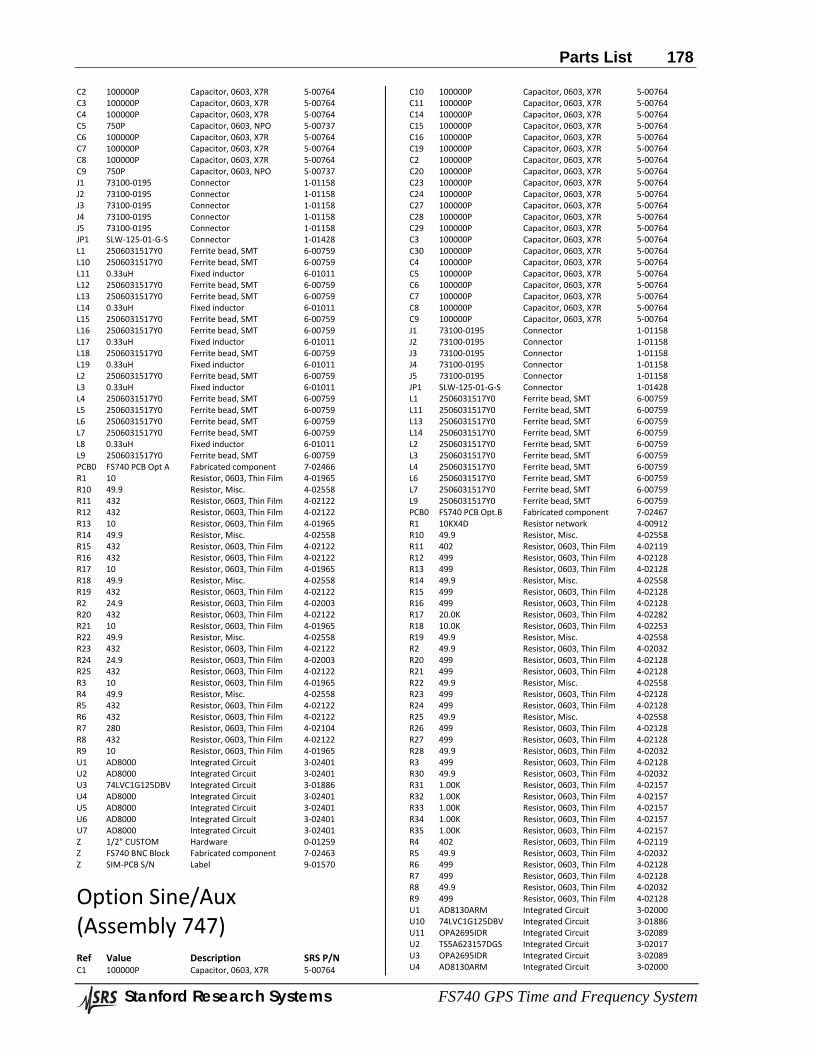
Parts List 178
Stanford Research Systems FS740 GPS Time and Frequency System
C2 100000P Capacitor, 0603, X7R 5-00764 C3 100000P Capacitor, 0603, X7R 5-00764 C4 100000P Capacitor, 0603, X7R 5-00764 C5 750P Capacitor, 0603, NPO 5-00737 C6 100000P Capacitor, 0603, X7R 5-00764 C7 100000P Capacitor, 0603, X7R 5-00764 C8 100000P Capacitor, 0603, X7R 5-00764 C9 750P Capacitor, 0603, NPO 5-00737 J1 73100-0195 Connector 1-01158 J2 73100-0195 Connector 1-01158 J3 73100-0195 Connector 1-01158 J4 73100-0195 Connector 1-01158 J5 73100-0195 Connector 1-01158 JP1 SLW-125-01-G-S Connector 1-01428 L1 2506031517Y0 Ferrite bead, SMT 6-00759 L10 2506031517Y0 Ferrite bead, SMT 6-00759 L11 0.33uH Fixed inductor 6-01011 L12 2506031517Y0 Ferrite bead, SMT 6-00759 L13 2506031517Y0 Ferrite bead, SMT 6-00759 L14 0.33uH Fixed inductor 6-01011 L15 2506031517Y0 Ferrite bead, SMT 6-00759 L16 2506031517Y0 Ferrite bead, SMT 6-00759 L17 0.33uH Fixed inductor 6-01011 L18 2506031517Y0 Ferrite bead, SMT 6-00759 L19 0.33uH Fixed inductor 6-01011 L2 2506031517Y0 Ferrite bead, SMT 6-00759 L3 0.33uH Fixed inductor 6-01011 L4 2506031517Y0 Ferrite bead, SMT 6-00759 L5 2506031517Y0 Ferrite bead, SMT 6-00759 L6 2506031517Y0 Ferrite bead, SMT 6-00759 L7 2506031517Y0 Ferrite bead, SMT 6-00759 L8 0.33uH Fixed inductor 6-01011 L9 2506031517Y0 Ferrite bead, SMT 6-00759 PCB0 FS740 PCB Opt A Fabricated component 7-02466 R1 10 Resistor, 0603, Thin Film 4-01965 R10 49.9 Resistor, Misc. 4-02558 R11 432 Resistor, 0603, Thin Film 4-02122 R12 432 Resistor, 0603, Thin Film 4-02122 R13 10 Resistor, 0603, Thin Film 4-01965 R14 49.9 Resistor, Misc. 4-02558 R15 432 Resistor, 0603, Thin Film 4-02122 R16 432 Resistor, 0603, Thin Film 4-02122 R17 10 Resistor, 0603, Thin Film 4-01965 R18 49.9 Resistor, Misc. 4-02558 R19 432 Resistor, 0603, Thin Film 4-02122 R2 24.9 Resistor, 0603, Thin Film 4-02003 R20 432 Resistor, 0603, Thin Film 4-02122 R21 10 Resistor, 0603, Thin Film 4-01965 R22 49.9 Resistor, Misc. 4-02558 R23 432 Resistor, 0603, Thin Film 4-02122 R24 24.9 Resistor, 0603, Thin Film 4-02003 R25 432 Resistor, 0603, Thin Film 4-02122 R3 10 Resistor, 0603, Thin Film 4-01965 R4 49.9 Resistor, Misc. 4-02558 R5 432 Resistor, 0603, Thin Film 4-02122 R6 432 Resistor, 0603, Thin Film 4-02122 R7 280 Resistor, 0603, Thin Film 4-02104 R8 432 Resistor, 0603, Thin Film 4-02122 R9 10 Resistor, 0603, Thin Film 4-01965 U1 AD8000 Integrated Circuit 3-02401 U2 AD8000 Integrated Circuit 3-02401 U3 74LVC1G125DBV Integrated Circuit 3-01886 U4 AD8000 Integrated Circuit 3-02401 U5 AD8000 Integrated Circuit 3-02401 U6 AD8000 Integrated Circuit 3-02401 U7 AD8000 Integrated Circuit 3-02401 Z 1/2" CUSTOM Hardware 0-01259 Z FS740 BNC Block Fabricated component 7-02463 Z SIM-PCB S/N Label 9-01570
Option Sine/Aux (Assembly 747) Ref Value Description SRS P/N C1 100000P Capacitor, 0603, X7R 5-00764
C10 100000P Capacitor, 0603, X7R 5-00764 C11 100000P Capacitor, 0603, X7R 5-00764 C14 100000P Capacitor, 0603, X7R 5-00764 C15 100000P Capacitor, 0603, X7R 5-00764 C16 100000P Capacitor, 0603, X7R 5-00764 C19 100000P Capacitor, 0603, X7R 5-00764 C2 100000P Capacitor, 0603, X7R 5-00764 C20 100000P Capacitor, 0603, X7R 5-00764 C23 100000P Capacitor, 0603, X7R 5-00764 C24 100000P Capacitor, 0603, X7R 5-00764 C27 100000P Capacitor, 0603, X7R 5-00764 C28 100000P Capacitor, 0603, X7R 5-00764 C29 100000P Capacitor, 0603, X7R 5-00764 C3 100000P Capacitor, 0603, X7R 5-00764 C30 100000P Capacitor, 0603, X7R 5-00764 C4 100000P Capacitor, 0603, X7R 5-00764 C5 100000P Capacitor, 0603, X7R 5-00764 C6 100000P Capacitor, 0603, X7R 5-00764 C7 100000P Capacitor, 0603, X7R 5-00764 C8 100000P Capacitor, 0603, X7R 5-00764 C9 100000P Capacitor, 0603, X7R 5-00764 J1 73100-0195 Connector 1-01158 J2 73100-0195 Connector 1-01158 J3 73100-0195 Connector 1-01158 J4 73100-0195 Connector 1-01158 J5 73100-0195 Connector 1-01158 JP1 SLW-125-01-G-S Connector 1-01428 L1 2506031517Y0 Ferrite bead, SMT 6-00759 L11 2506031517Y0 Ferrite bead, SMT 6-00759 L13 2506031517Y0 Ferrite bead, SMT 6-00759 L14 2506031517Y0 Ferrite bead, SMT 6-00759 L2 2506031517Y0 Ferrite bead, SMT 6-00759 L3 2506031517Y0 Ferrite bead, SMT 6-00759 L4 2506031517Y0 Ferrite bead, SMT 6-00759 L6 2506031517Y0 Ferrite bead, SMT 6-00759 L7 2506031517Y0 Ferrite bead, SMT 6-00759 L9 2506031517Y0 Ferrite bead, SMT 6-00759 PCB0 FS740 PCB Opt.B Fabricated component 7-02467 R1 10KX4D Resistor network 4-00912 R10 49.9 Resistor, Misc. 4-02558 R11 402 Resistor, 0603, Thin Film 4-02119 R12 499 Resistor, 0603, Thin Film 4-02128 R13 499 Resistor, 0603, Thin Film 4-02128 R14 49.9 Resistor, Misc. 4-02558 R15 499 Resistor, 0603, Thin Film 4-02128 R16 499 Resistor, 0603, Thin Film 4-02128 R17 20.0K Resistor, 0603, Thin Film 4-02282 R18 10.0K Resistor, 0603, Thin Film 4-02253 R19 49.9 Resistor, Misc. 4-02558 R2 49.9 Resistor, 0603, Thin Film 4-02032 R20 499 Resistor, 0603, Thin Film 4-02128 R21 499 Resistor, 0603, Thin Film 4-02128 R22 49.9 Resistor, Misc. 4-02558 R23 499 Resistor, 0603, Thin Film 4-02128 R24 499 Resistor, 0603, Thin Film 4-02128 R25 49.9 Resistor, Misc. 4-02558 R26 499 Resistor, 0603, Thin Film 4-02128 R27 499 Resistor, 0603, Thin Film 4-02128 R28 49.9 Resistor, 0603, Thin Film 4-02032 R3 499 Resistor, 0603, Thin Film 4-02128 R30 49.9 Resistor, 0603, Thin Film 4-02032 R31 1.00K Resistor, 0603, Thin Film 4-02157 R32 1.00K Resistor, 0603, Thin Film 4-02157 R33 1.00K Resistor, 0603, Thin Film 4-02157 R34 1.00K Resistor, 0603, Thin Film 4-02157 R35 1.00K Resistor, 0603, Thin Film 4-02157 R4 402 Resistor, 0603, Thin Film 4-02119 R5 49.9 Resistor, 0603, Thin Film 4-02032 R6 499 Resistor, 0603, Thin Film 4-02128 R7 499 Resistor, 0603, Thin Film 4-02128 R8 49.9 Resistor, 0603, Thin Film 4-02032 R9 499 Resistor, 0603, Thin Film 4-02128 U1 AD8130ARM Integrated Circuit 3-02000 U10 74LVC1G125DBV Integrated Circuit 3-01886 U11 OPA2695IDR Integrated Circuit 3-02089 U2 TS5A623157DGS Integrated Circuit 3-02017 U3 OPA2695IDR Integrated Circuit 3-02089 U4 AD8130ARM Integrated Circuit 3-02000
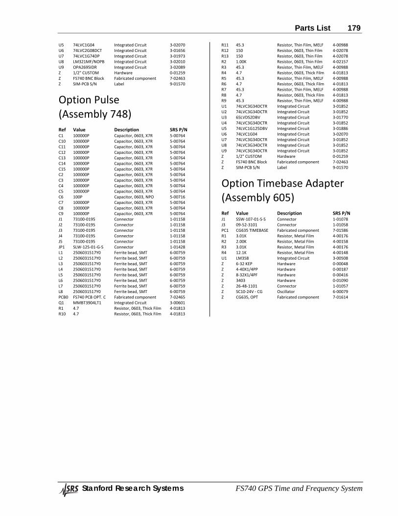
Parts List 179
Stanford Research Systems FS740 GPS Time and Frequency System
U5 74LVC1G04 Integrated Circuit 3-02070 U6 74LVC2G08DCT Integrated Circuit 3-01656 U7 74LVC1G74DP Integrated Circuit 3-01973 U8 LM321MF/NOPB Integrated Circuit 3-02010 U9 OPA2695IDR Integrated Circuit 3-02089 Z 1/2" CUSTOM Hardware 0-01259 Z FS740 BNC Block Fabricated component 7-02463 Z SIM-PCB S/N Label 9-01570
Option Pulse (Assembly 748) Ref Value Description SRS P/N C1 100000P Capacitor, 0603, X7R 5-00764 C10 100000P Capacitor, 0603, X7R 5-00764 C11 100000P Capacitor, 0603, X7R 5-00764 C12 100000P Capacitor, 0603, X7R 5-00764 C13 100000P Capacitor, 0603, X7R 5-00764 C14 100000P Capacitor, 0603, X7R 5-00764 C15 100000P Capacitor, 0603, X7R 5-00764 C2 100000P Capacitor, 0603, X7R 5-00764 C3 100000P Capacitor, 0603, X7R 5-00764 C4 100000P Capacitor, 0603, X7R 5-00764 C5 100000P Capacitor, 0603, X7R 5-00764 C6 100P Capacitor, 0603, NPO 5-00716 C7 100000P Capacitor, 0603, X7R 5-00764 C8 100000P Capacitor, 0603, X7R 5-00764 C9 100000P Capacitor, 0603, X7R 5-00764 J1 73100-0195 Connector 1-01158 J2 73100-0195 Connector 1-01158 J3 73100-0195 Connector 1-01158 J4 73100-0195 Connector 1-01158 J5 73100-0195 Connector 1-01158 JP1 SLW-125-01-G-S Connector 1-01428 L1 2506031517Y0 Ferrite bead, SMT 6-00759 L2 2506031517Y0 Ferrite bead, SMT 6-00759 L3 2506031517Y0 Ferrite bead, SMT 6-00759 L4 2506031517Y0 Ferrite bead, SMT 6-00759 L5 2506031517Y0 Ferrite bead, SMT 6-00759 L6 2506031517Y0 Ferrite bead, SMT 6-00759 L7 2506031517Y0 Ferrite bead, SMT 6-00759 L8 2506031517Y0 Ferrite bead, SMT 6-00759 PCB0 FS740 PCB OPT. C Fabricated component 7-02465 Q1 MMBT3904LT1 Integrated Circuit 3-00601 R1 4.7 Resistor, 0603, Thick Film 4-01813 R10 4.7 Resistor, 0603, Thick Film 4-01813
R11 45.3 Resistor, Thin Film, MELF 4-00988 R12 150 Resistor, 0603, Thin Film 4-02078 R13 150 Resistor, 0603, Thin Film 4-02078 R2 1.00K Resistor, 0603, Thin Film 4-02157 R3 45.3 Resistor, Thin Film, MELF 4-00988 R4 4.7 Resistor, 0603, Thick Film 4-01813 R5 45.3 Resistor, Thin Film, MELF 4-00988 R6 4.7 Resistor, 0603, Thick Film 4-01813 R7 45.3 Resistor, Thin Film, MELF 4-00988 R8 4.7 Resistor, 0603, Thick Film 4-01813 R9 45.3 Resistor, Thin Film, MELF 4-00988 U1 74LVC3G34DCTR Integrated Circuit 3-01852 U2 74LVC3G34DCTR Integrated Circuit 3-01852 U3 65LVDS2DBV Integrated Circuit 3-01770 U4 74LVC3G34DCTR Integrated Circuit 3-01852 U5 74LVC1G125DBV Integrated Circuit 3-01886 U6 74LVC1G04 Integrated Circuit 3-02070 U7 74LVC3G34DCTR Integrated Circuit 3-01852 U8 74LVC3G34DCTR Integrated Circuit 3-01852 U9 74LVC3G34DCTR Integrated Circuit 3-01852 Z 1/2" CUSTOM Hardware 0-01259 Z FS740 BNC Block Fabricated component 7-02463 Z SIM-PCB S/N Label 9-01570
Option Timebase Adapter (Assembly 605) Ref Value Description SRS P/N J1 SSW-107-01-S-S Connector 1-01078 J3 09-52-3101 Connector 1-01058 PC1 CG635 TIMEBASE Fabricated component 7-01586 R1 3.01K Resistor, Metal Film 4-00176 R2 2.00K Resistor, Metal Film 4-00158 R3 3.01K Resistor, Metal Film 4-00176 R4 12.1K Resistor, Metal Film 4-00148 U1 LM358 Integrated Circuit 3-00508 Z 6-32 KEP Hardware 0-00048 Z 4-40X1/4PP Hardware 0-00187 Z 8-32X1/4PF Hardware 0-00416 Z 3403 Hardware 0-01090 Z 26-48-1101 Connector 1-01057 Z SC10-24V - CG Oscillator 6-00079 Z CG635, OPT Fabricated component 7-01614

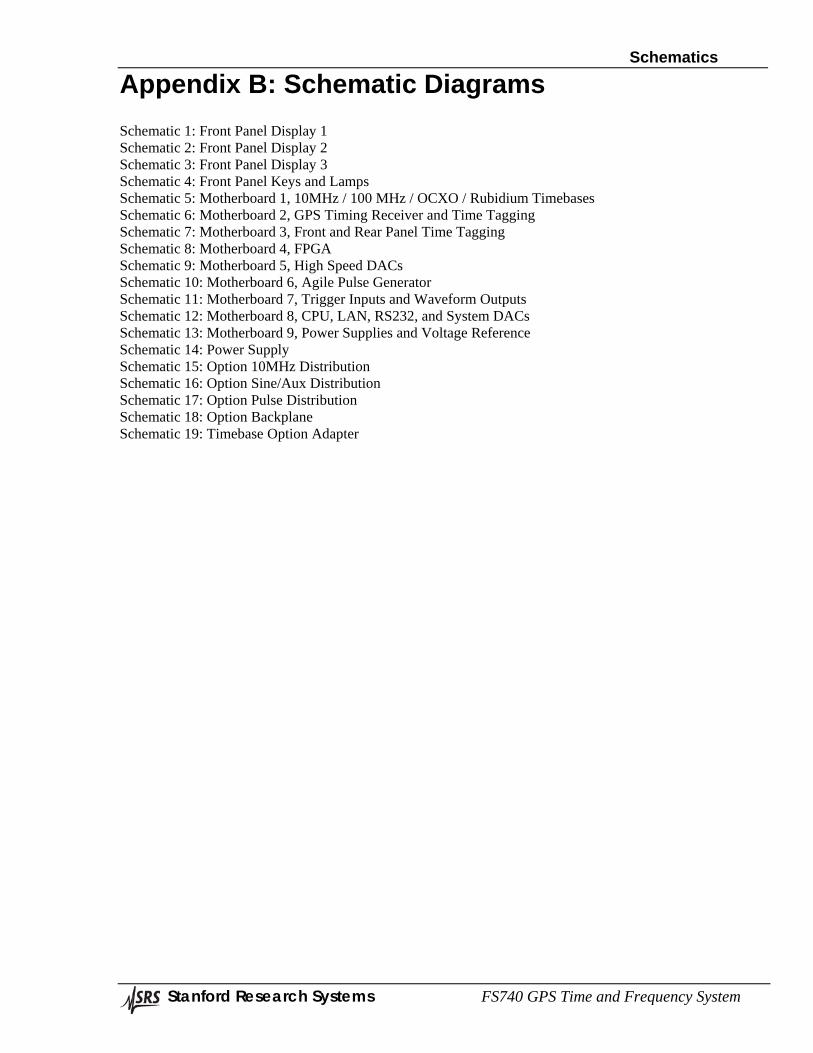
Schematics
Stanford Research Systems FS740 GPS Time and Frequency System
Appendix B: Schematic Diagrams Schematic 1: Front Panel Display 1 Schematic 2: Front Panel Display 2 Schematic 3: Front Panel Display 3 Schematic 4: Front Panel Keys and Lamps Schematic 5: Motherboard 1, 10MHz / 100 MHz / OCXO / Rubidium Timebases Schematic 6: Motherboard 2, GPS Timing Receiver and Time Tagging Schematic 7: Motherboard 3, Front and Rear Panel Time Tagging Schematic 8: Motherboard 4, FPGA Schematic 9: Motherboard 5, High Speed DACs Schematic 10: Motherboard 6, Agile Pulse Generator Schematic 11: Motherboard 7, Trigger Inputs and Waveform Outputs Schematic 12: Motherboard 8, CPU, LAN, RS232, and System DACs Schematic 13: Motherboard 9, Power Supplies and Voltage Reference Schematic 14: Power Supply Schematic 15: Option 10MHz Distribution Schematic 16: Option Sine/Aux Distribution Schematic 17: Option Pulse Distribution Schematic 18: Option Backplane Schematic 19: Timebase Option Adapter
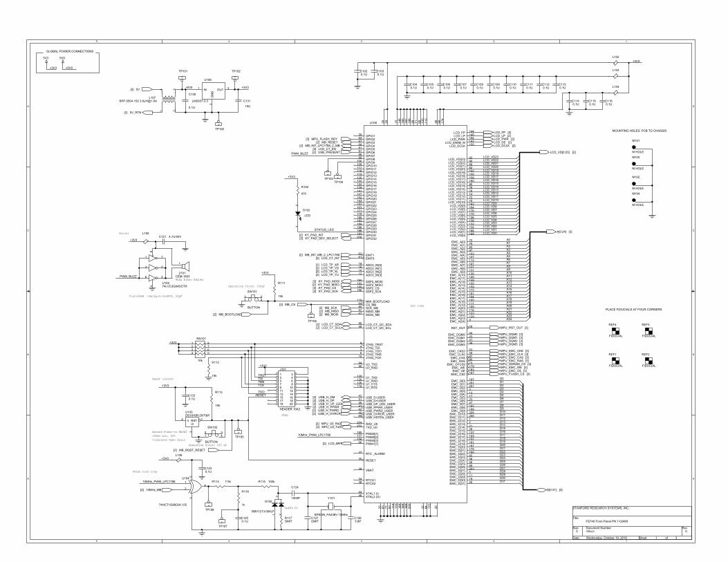
5
5
4
4
3
3
2
2
1
1
D D
C C
B B
A A
Reset circuit
Extend Power-on RESET100ms min. 20%tolerance Open drain
+-
Buzzer
GLOBAL POWER CONNECTIONS
MOUNTING HOLES: PCB TO CHASSIS
Phase Lock Loop
PLACE FIDUCIALS AT FOUR CORNERS
Iout=32mA tdelay=3.2ns@5V, 50pF
4kHz Piezo Xducer
Operating force: 100 gf
Operating force: 100gf
JTAG
<Doc> C
FS740 Front Panel PN 7-02460
STANFORD RESEARCH SYSTEMS, INC.
C
1 3Wednesday, October 19, 2016
Title
Size Document Number Rev
Date: Sheet of
+3V3
+3V3
+3V3
10MHz_PWM_LPC1788
+3V3
+3V3
PWM_BUZZ
TCK
D11
D16
A4
LCD_VD22LCD_VD21
A2
D15
D10
A13
A11
A17
D14
D5
D3
LCD_VD4
LCD_VD19
D28
A3
A20
A12
A8
LCD_VD14
-RESET
D27
LCD_VD7
LCD_VD0
A10
LCD_VD13
A0
LCD_VD11
D24
D29
TRST
D1
A15
D18
A22
A18
A16
LCD_VD23
D26
D30
TDI
A14
LCD_VD5
LCD_VD3
A1
D12
D2
D6
D8
D21
LCD_VD2
A19
A5
A24
TMS
D19
LCD_VD16
D17
A23
D9
D22
A7
LCD_VD15
D13
TDO
D0
A21
LCD_VD20
D7
A9
A6
LCD_VD10
D23
D31
10MHz_PWM_LPC1788
LCD_VD8LCD_VD9
LCD_VD12
D25
LCD_VD6
D20
LCD_VD1
LCD_VD17LCD_VD18
D4
+3V3
+3V3
+3V3
+3V3
STATUS_LED
PWM_BUZZ
+5V0
+5V0
+5V0
5V03V3
C1080.1U
R111
10k
C1160.1U
Y101
EPSON_FA238V 12MHzC1250.1U
Z101CEM-1603
L107SRF-0504-152 [email protected]
1 234
U104
74HCT1G86GW,125
1
2
3
4
5
.
..
C1110.1U
TP102
1
C1150.1U
U106
LM2937-3.3
1
2
3IN
GN
D
OUT
C1060.1U
C1265.6P
TP109
1
C127OMIT
D102
LED
21
TP105
1
C1140.1U
C121 4.7U/50V
C130
0.1U
TP108
1
C1090.1U
TP103
1
SW101
BUTTON
12 3
4.. .
.LPC 1788
U105
1
2
3
4
5
6
7
8
9
10
11
12
13
14
15
16
17
18
19
20
21
22
23
24
25
26
27
28
29
30
31
3233
34
35
36
37
38
39
40
4142
43
44
45
46
47
50
49
48
5152
53
54
5556
57
58
59
60
6162
63
64
65
66
6768
69
70
71
72
73
74
75
76
77
78
79
80
81
82
83
84
85
86
87
88
89
90
91
92
93
9495
96
97
9899
100
101
102
103
104105
106
107
108
109
110111
112
113
114
115
116
117118119120
121
122
123
124
125
126
127
128
129
130
131
132
133
134
135
136
137
138
139
140
141
142
143
144
145
146
147
148
149
150
151
152153
154
155
156
157
158
159
160
161
162163 164
165
166
167
168
169
170171
172
173
174
175
176
177
178
179
180
181
182
183
184
185
186
187
188
189
190
191
192
193
194
195
196
197
198
19920
0
201
202
203
204
205
206
207
208EMC_D[12]
JTAG_TDO
EMC_D[3]
JTAG_TDI
EMC_D[28]
JTAG_TMS
EMC_D[13]
JTAG_TRST
EMC_A[24]
JTAG_TCK
EMC_D[29]
ADC0_IN[3]
EMC_D[4]
ADC0_IN[2]ADC0_IN[1]
EMC_D[5]
ADC0_IN[0]
EMC_D[30]
EMC_D[14]
EMC_D[6]
EMC_D[31]
EMC_D[7]
EMC_D[15]
RST_OUT
GPIO1
EMC_DQM2
RTCX1
RESET
RTCX2
RTC _ALARM
VBAT
EMC_DQM3
USB_OVRCR_USER
USB_PPWR_USERUSB_PWRD_USER
EMC_DQM1
XTAL1 (I)
USB_UP_LED_USER
XTAL2 (O)
MOSI_MB
LCD_CT_I2C_SDA
EMC_DQM0
LCD_CT_I2C_SCL
USB_D+USERUSB_D-USER
EMC_CKE0
GPIO2
EMC_D[26]EMC_D[25]
MISO_MB
EMC_D[24]
EMC_CLK0
EINT0EINT1
CS_MB
EMC_D[23]
PWM1[1]
GPIO3GPIO4
USB_HSTEN_USER
LCD_VD[10]LCD_VD[11]
EMC_DYCS0
LCD_VD[12]
EMC_A[0]
LCD_VD[13]LCD_VD[14]
EMC_A[1]
LCD_VD[15]
GPIO5
LCD_VD[20]
EMC_A[2]
SCK_MB
EMC_CAS
LCD_VD[21]LCD_VD[22]
GPIO6
LCD_VD[23]
U3_TXDEMC_RAS
U3_RXD
EMC_A[3]
GPIO7GPIO8GPIO9
EMC_A[16]
LCD_VD[19]
EMC_A[4]
EMC_A[17]EMC_A[18]
LCD_VD[18]
EMC_A[5]
GPIO10
EMC_A[20]
NMI_BOOTLOADEMC_A[19]
EMC_A[6]
EMC_A[21]
U1_RTS
GPIO11GPIO12GPIO13GPIO14
EMC_A[7]
GPIO15
EMC_A[22]
GPIO16
U1_CTS
EMC_A[8]
U1_TXD
EMC_A[23]
U1_RXD
EMC_A[9]
LCD_VD[3]LCD_VD[2]
EMC_A[10]
LCD_VD[5]
EMC_D[16]
LCD_VD[4]
GPIO17
LCD_LP
GPIO18
LCD_ENAB_M
EMC_D[17]
LCD_FP
EMC_A[11]
GPIO19
EMC_A[12]
LCD_DCLK
EMC_D[18]
GPIO20GPIO21
LCD_PWR
EMC_A[13]
PWM0[3]
GPIO22
LCD_VD[17]
EMC_A[14]
LCD_VD[16]
EMC_D[19]
LCD_VD[9]GPIO23 LCD_VD[8]
LCD_VD[1]
EMC_D[20]
LCD_VD[0]
LCD_VD[6]GPIO24
EMC_A[15]
EMC_D[21]
LCD_VD[7]
PWM0[2]
GPIO25
EMC_WE
GPIO26GPIO27
EMC_OE
GPIO28
PWM0[1]
GPIO29
EMC_CS0
GPIO30
SSP2_CS
EMC_D[8]
SSP2_MISO
GPIO31
SSP2_MOSI
EMC_D[22]
SSP2_SCK
EMC_D[0]
EMC_D[9]
EMC_D[1]
TXD_U0
EMC_D[27]
RXD_U0
EMC_D[10]
GPIO32
EMC_D[2]
EMC_D[11]
D105
SMV1213-004LF
1 23
TP104
1
C1040.1U
R112
10k
C124
1000P
TP106
1
L102
REF2
FIDUCIAL
C1220.1U
C131
15U
C1120.1U
SW102
BUTTON
12 3
4.. .
.
R115 100k
C1070.1U
C1020.1U
-
+
U10274LVC3G04DCTR
1
4
3
8
5
7
6 2
REF3
FIDUCIAL
R116
1k
R102
470
C1030.1U
J101
HEADER 10X2
1 23 45 67 89 1011 1213 1415 1617 1819 20
L104
RN101
10k
1234 5
678
L105
C1100.1U
TP107
1
R114 7.5k
C1050.1U
R113
10k
M101
M HOLE
TP101
1
M102
M HOLE
C1230.1U
REF4
FIDUCIAL
M103
M HOLE
M104
M HOLE
U103DS1816R-20/T&R
12
3
RSTV
G
C1130.1U
L106
L103
R117OMIT
REF1
FIDUCIAL
LCD_FP [2]
LCD_PWR [2]
MPU_RST_OUT [3]
MPU_DQM0 [3]MPU_DQM1 [3]MPU_DQM2 [3]MPU_DQM3 [3]
A[0:24] [3]
D[0:31] [3]
MPU_EMC_RAS [3]MPU_SDRAM_CS [3]
MPU_EMC_CAS [3]MPU_EMC_CLK [3]MPU_EMC_CKE [3]
MB_RQST_RESET[2]
5V[2]
5V_RTN[2]
MB_BOOTLOAD[2]
MPU_FLASH_CS [3]MPU_EMC_OE [3]MPU_EMC_WE [3]
LCD_DE [2]LCD_DCLK [2]
10MHz_MB[2]
LCD_VD[0:23] [2]
LCD_LP [2]
MB_MOSI[2]
MB_CS[2]
LCD_TP_YU[2]
MPU_FLASH_RDY[3]
USB_H_OVRCR[2]
MB_SCK[2]
MB_RESET[2]
LCD_BRT[2]
USB_H_DM[2]
USB_H_PWRD[2]USB_H_PPWR[2]
MB_INT_LPC1788_2_MB[2]
USB_H_UP_LED[2]
MPU_U0_TxD[2]
USB_H_DP[2]
LCD_CT_SDA[2]
MPU_U0_RxD[2]
LCD_TP_XR[2]
LCD_CT_EN[2]
LCD_TP_YD[2]LCD_TP_XL[2]
USB_PRESENT[2]
LCD_CT_SCL[2]
MB_INT_MB_2_LPC1788[2]LCD_CT_INT[2]
MB_MISO[2]
KY_PAD_DEV_SELECT[2]KY_PAD_INT[2]
KY_PAD_MOSI[2]
KY_PAD_CS[2]KY_PAD_SCK[2]
KY_PAD_MISO[2]
5
5
4
4
3
3
2
2
1
1
D D
C C
B B
A A
LCD backlight voltage generator
Capacitive touch Interface I2C
Motherboard Connector
Micro-USB
GLOBAL POWER CONNECTIONS
Program FTX230 CBUS0 = -PWREN CBUS1 = Rx LED CBUS2 = Tx LED CBUS3 =-KEEP_AWAKE
Terminate LVDS
1.2 VMAX
Irated>40mA
LCD isNHD-4.3-480272EF-ATXL#-CTP
Multiplexer shown in OFF position(3 - Low => 0 goes to 4)
USB Host expasion board connector.
Murata LQH32PN150MN0DCR:0.57 Imax:0.5A
USB 2.0 Basic UART
KEYPAD SPI Communication port
LCD connector
<Doc> C
FS740 Front Panel 7-02460
STANFORD RESEARCH SYSTEMS, INC.
C
2 3Wednesday, October 19, 2016
Title
Size Document Number Rev
Date: Sheet of
+3V3
+10MHz_MB
RxD_MB
-10MHz_MB
TxD_MB
TxD_USB
+5V_RTN
+5V0
+3V3
ANODE+5V0
CATHODE
LCD_VD0
LCD_VD6LCD_VD5
LCD_VD2LCD_VD1
LCD_VD3LCD_VD4
LCD_VD7
LCD_VD13
LCD_VD10
LCD_VD8
LCD_VD11LCD_VD12
LCD_VD9
LCD_VD17
LCD_VD15LCD_VD16
LCD_VD20LCD_VD19
LCD_VD14
LCD_VD18
LCD_VD21LCD_VD22LCD_VD23
+3V3
+3V3
RxD_USBTxD_MB
-PWREN+5V
RxD_MB
+3V3
+3V3
SIGNAL_GND
+3V3
+5V0+3V3
3V3 5V0
J204
MOLEX_40pin_0.5mmpitch
123456789
10111213141516171819202122232425262728293031323334353637383940
4142
LED-LED+GNDVDDR0R1R2R3R4R5R6R7G0G1G2G3G4G5G6G7B0B1B2B3B4B5B6B7GNDCLKDISPHSYNCVSYNCDENCGNDXRYDXLYU
PADPAD0
1
S G
V
U20374LVC1G3157
3
1
6 2
4
5
R216
10k
R206
910k
C2010.1U
J206
HEADER-8
12345678
L203 15 U1 2
J201
HEADER 16
123456789
10111213141516
C2080.01U
R212 33
R217
10k
R211 33
0
1
S G
V
U20274LVC1G3157
3
1
6 2
4
5
C2110.1U
U205 FT230XQ15
1612
3
4
5
67
8
9
10
131112
1417
TXD
RTSVCCIORXD
GND
CTS
CBUS2
USBDPUSBDM
3V3OUT
RESET
VCC
GNDCBUS1CBUS0
CBUS3PAD
J202
CON10
12345678910
TP201
1
C2090.1U
L205
TP202
1
J205
Molex_6Pin_1mm_pitch
1
2
3
4
5
6
78
SCL
SDA
INT
WAKE
PADPAD
D201
MBRX160
TP203
1
C20610U
TP204
1
L204
BEAD
R213
10k
C2041U U204
PAM2841
1
2
3
4 5
6
7
8PGND
VIN
ENA
COMP GND
FB
OVP
SW
R208
27k
C21010U
C213
47P
R207
5.1
C2050.1U
R205
10k
C2121U
G
U201
SN65LVDS2
3
45
12
R224 100
L202
R201
10k
R223 OMIT
R222 OMIT
C214
47P
C2071U
J203
FTDI10103594-0001LF
12345
6789
5V_USBD-D+ID
GND
CHGNDCHGNDCHGNDCHGND
L201
MB_RESET [1]MB_RQST_RESET [1]
MB_SCK [1]
10MHz_MB [1]
MB_CS [1]
MB_BOOTLOAD [1]
MB_MISO [1]MB_MOSI [1]
LCD_BRT[1]
LCD_VD[0:23][1]
LCD_CT_INT[1]
LCD_CT_SCL[1]
LCD_CT_EN[1]
LCD_CT_SDA[1]
5V_RTN [1]5V [1]
LCD_DCLK[1]
LCD_TP_XL[1]
LCD_LP[1]LCD_PWR[1]
LCD_TP_XR[1]
LCD_FP[1]
LCD_TP_YD[1]
LCD_DE[1]
MB_INT_MB_2_LPC1788 [1]
USB_PRESENT [1]
MB_INT_LPC1788_2_MB [1]
USB_H_UP_LED[1]
USB_H_PPWR[1]USB_H_PWRD[1]USB_H_DP[1]USB_H_DM[1]
USB_H_OVRCR[1]
KY_PAD_DEV_SELECT[1]
KY_PAD_INT[1]KY_PAD_MOSI[1]KY_PAD_MISO[1]KY_PAD_SCK[1]KY_PAD_CS[1]
MPU_U0_TxD [1]
MPU_U0_RxD [1]
LCD_TP_YU[1]
5
5
4
4
3
3
2
2
1
1
D D
C C
B B
A A
FLASH MODE INPUT PINSBYTE selects data buswidth (VIH wordconfig) WP WriteProtection (VIH toenable programming)
SDRAM 32MB (8M x 32)
GLOBAL POWER CONNECTIONS
NOR-FLASH 256 Megabit (32 MB)
<Doc> C
FS740 Front Panel 7-02460
STANFORD RESEARCH SYSTEMS, INC.
C
3 3Wednesday, October 19, 2016
Title
Size Document Number Rev
Date: Sheet of
-WE
D9
D2
D14
D21
D12D11
D1
D16D15D14
D5
D24
D7
D2
D0
D22
D5
D12
D25
D4
D7
D15
D30D29
D4
D27D26
D3
D17D13
D20
D23
D10
D28
D18
D8
D6
D0
D10
D11
D19
D31
D13
D1
D8
D3
D6
D9
-WE
A7
A3
A10
A22
A14
A12
A3A2A4
A11A12
A11
A2
A5
A15
A8
A13
A17A16
A6A5
A1
A19
A9
A9
A18
A10
A14
A0
A23A24
A20
A1
A4
A8A7
A6
A21
A13
+3V3
+3V3
+3V3
+3V3
3V3
C3080.1U
L301
BEAD
C3130.1U
C3030.1U
C3050.1U
C3070.1U
C3110.1U
C3120.1U
C3010.1U
R301 10k
U302
IS42S32800D-7
1
2
3
45
6
78
9
1011
12
13
14
15
16
17
1819
20
21
2223
24
252627
28
29
30
31
32
3334
35
3637
38
3940
41
42
43
44
45
46
4748
49
5051
52
5354
55
56
57
58
59
60616263646566
67
68
69
70
71
72
73
74
75
7677
78
7980
81
8283
84
85
86
VDD
DQ0
VDDQ
DQ1DQ2
VSSQ
DQ3DQ4
VDDQ
DQ5DQ6
VSSQ
DQ7
NC
VDD
DQM0
WE
CASRAS
CS
A11
BA0BA1
A10
A0A1A2
DQM2
VDD
NC
DQ16
VSSQ
DQ17DQ18
VDDQ
DQ19DQ20
VSSQ
DQ21DQ22
VDDQ
DQ23
VDD
VSS
DQ24
VSSQ
DQ25DQ26
VDDQ
DQ27DQ28
VSSQ
DQ29DQ30
VDDQ
DQ31
NC
VSS
DQM3
A3A4A5A6A7A8A9
CKE
CLK
A12
NC
DQM1
VSS
NC
DQ8
VDDQ
DQ9DQ10
VSSQ
DQ11DQ12
VDDQ
DQ13DQ14
VSSQ
DQ15
VSS
L303
BEAD
L302
BEADC3040.1U
C3060.1U
C3100.1U
C3020.1U
U301
S29GL256P
12
3456789
10
1112
13
14
15
16
171819
20212223242526
2728
29
30
31
32
33
34
35
36
37
38
39
40
41
42
43
44
45
46
47
48
49
50
51
52
53
54
5556A23
A22
A15A14A13A12A11A10A9A8
A19A20
WE
RESET
A21
WP
RYA18A17
A7A6A5A4A3A2A1
NCNCNC
A0
CEOE
DQ0
DQ8
DQ1
DQ9
DQ2
DQ10
DQ3
DQ11
DQ4
DQ12
DQ5
DQ13
DQ6
DQ14
DQ7
DQ15A-1
BYTE
A16
NCNC
R302 10k
C3090.1U
C3140.1U
D[0:31][1]
A[0:24][1]
MPU_EMC_CKE[1]
MPU_EMC_CLK[1]
MPU_DQM0[1]MPU_DQM1[1]MPU_DQM2[1]MPU_DQM3[1]
MPU_EMC_CAS[1]MPU_EMC_RAS[1]
MPU_EMC_WE[1]MPU_SDRAM_CS[1]
MPU_FLASH_CS[1]MPU_EMC_OE[1]
MPU_RST_OUT[1]
MPU_FLASH_RDY [1]
5
5
4
4
3
3
2
2
1
1
D D
C C
B B
A A
Line 3 of connector is A0, 1-bit address formultiple SPI slaves support. This feature notused here.
Shift register has 24 bit positions, numbered [0 - 23] [0-13] LED drivers [13-15] Not connected [16-23] Push buttons
4-40 MOUNTING HOLES FOR PCB:
SW REF. | FUNCTION | Shift Reg. Position SW101 Status 16 SW102 Sine out 17 SW103 GPS 18 SW104 Aux Out 19 SW105 DIST AMPS 20 SW106 Pulse Out 21 SW107 Config 22 SW108 Time or Freq In 23
LED: Anode => pin1 Cathode=> pin 2
LED REF. | FUNCTION | COLOR | Shift Reg. PositionD101 Status-Power Green 0 D102 Status-Tracking Green 1 D103 Status-Fault Red 2 D104 GPS-Antenna Yellow 3 D105 GPS-1PPS Yellow 4 D106 GPS-Fault Yellow 5 D107 DIST AMPS-Top Green 6 D108 DIST AMPS-Middle Red 7 D109 DIST AMPS-BottomYellow 8 D110 Config-COM ACT Green 9 D111 Config-COM ERR Red 10 D112 Config-Alarm Red 11 D113 FRONT-Trig Green 12 D114 REAR-Trig Green 13
PLACE FIDUCIALS AT FOUR CORNERS
Buffer/Inverter
3-state output
Push-pull output
Non-inverting configuration with hysteresis
COMPARATOR FORKEYPRESSDETECTION.
In- Vref 3.17V In+ Vin [0V - 3V] dVin = 0.66V
GPS KEYS AND LAMPS.DSN A
FS740 FRONT PANEL KEYS AND LAMPS 7-02461
C
1 1Friday, September 23, 2016
Title
Size Document Number Rev
Date: Sheet of
+3.3
+3.3
MISOMOSI
-CS_FRONT
+3.3
KEYPRESS
SCK
RN104A4x10K
18
V
G
U10674LVC2G08
1
2
3
45
6
78
D10
9
M2HOLE4-40
1
45
116
U10274HC165A
1011121314345612
15 8
7
9
16SID0D1D2D3D4D5D6D7S/-LCLKINH GND
Q
Q
VCC
D10
32
15
D10
5
R10220.0K
C101
.1U
U10374LVC1G125
2 4
135
RN103A4x10K
18
314
27
D10
1
C103
.1U
SW
102
12
34
J101HEADER-8
12345678
D11
4
U10474HC595A
16141110
15123456798
1312
VCCSICLKCLR
Q0Q1Q2Q3Q4Q5Q6Q7SOGND
OERCK
M3HOLE4-40
1
SW
103
12
34
D10
6
R104499
D11
3
SW
104
12
34
413
SW
108
12
34
-
+
U10174LVC2G04
1
2
3
5
4
6
+
-
V
GU107ADCMP371
1
2
34
5
512
27
SW
107
12
34
M1HOLE4-40
16
11
SW
105
12
34
SW
101
12
34
SW
106
12
34
710
611
D11
12
15
RN101H
8x100
89
116
REF3
FIDUCIAL
314
D11
2
36
U10574HC595A
16141110
15123456798
1312
VCCSICLKCLR
Q0Q1Q2Q3Q4Q5Q6Q7SOGND
OERCK
512
C104
.1U
R10149.9K
D10
4
413
C102
.1U
RN102H
8x100
89
36
REF4
FIDUCIAL
45
710
D11
0
D10
7
R103499
D10
8
REF1
FIDUCIAL
D10
2
5
5
4
4
3
3
2
2
1
1
D D
C C
B B
A A
100MHZ VCXO PHASELOCKED TO 20MHZTIMEBASE. 7.8kHZBANDWIDTH, 75DEGREE PHASEMARGIN.
OPERATE WITH Icp = 5.0mA.R= 5 AND N=1
2.5KHZ/V
HEADER TOOPTIONAL 10MHZTIMEBASE(RUBIDIUM OROCXO).
(LM340-12 AND TIP107 ARE TO-220 HEATERS)TEMPERATURE CONTROLLER FOR AT-CUT XTAL.
0 TO 100 mA, 0 TO 2.4 WATTS.
ABOUT 12 VDC
PROPORTIONAL &INTEGRALTEMPERATURECONTROLLER
LOW NOISE REGULATOR FOR 100 MHzVCXO AND 100 MHz DISTRIBUTION.
1 Vrms REAR10MHZSINEWAVEOUTPUT.TERMINATEINTO 50 OHMS.
100MHZ SINEWAVEFOR AUX OUT.
120 MHZ LOW PASS FILTER WITH NOTCHES AT 200MHZAND 300MHZ TO REDUCE SINE DISTORTION.
CLAMP AMP OUTPUT IS A LOW NOISE 20 MHzSQUAREWAVE WITH AMPLITUDE OF 5.3 Vpp.
UART: MASTER OUT,RUBIDIUM IN
UART: MASTER IN,RUBIDIUM OUT
GLOBAL POWER CONNECTIONS
GAIN = +5.0
+0.53VDC
-0.53VDC
ABOUT 1.6 VppACROSSDIFFERENTIALLOAD.
LONG INSULATEDLEAD/SPRING FORCESCONTACT WITH TIP107.
100K, NTC. ABOUT30k AT 55C.
0-4.095V
2V
NOM: 3.3V
POSITIVE FEEDBACK:OFFSET FORAMBIENT.
PROTECT Vbe.
LOW NOISE PHASELOCK LOOP BETWEEN10MHZ SOURCES.
300 kHz PRE-FILTER
LVDS 10 MHZ CLOCK TOSYNC GUI PROCESSOR.
THIS 20 MHZ, 3RD O.T.CRYSTAL OSCILLATOR MAY BEPLL'd TO THE OPTIONAL OCXOOR RUBIDIUM TIMEBASES.
UPPER TURNINGPOINT AT 55C.
4 mABIAS
FUNDAMENTALTRAP
MAINTAIN COLPITTS BIASCURRENT AT 4.0 mA
MAINTAIN COLPITTS BIASVOLTAGE AT ABOUT 3.2V
CMOS SOURCE RESISTANCE (AS GENERATORFOR LOW PASS FILTER) IS ABOUT 20 OHMS.
5TH ORDER CAUER LOW PASS FILTER (TO 11 MHZ) WITHNOTCH AT 30 MHZ (TO SQUASH 3RD HARMONIC).
PLL LOOP FILTER. WHEN DAC/-PLL IS HIGH, THE EFC OUTPUTFOLLOWS "BIG_DAC". WHEN DAC/-PLL IS LOW, EFC OUTPUT IS PLLLOOP FILTER TO LOCK 20MHZ TCXO TO OCXO OR RUBIDIUM TIMEBASE.
200 OHMS => 50 OHMS
IN CG635, Cbe = 56P,Ltrap = .47UH. (VALUESABOVE FROM SG3XX.)
LOW-NOISE CMOS DIVIDE-BY-TWO PROVIDES10MHZ SOURCES. SLOW 74HC74 USED FORREDUCED NOISE BANDWIDTH OF CLOCK INPUT.
200 OHMS => 50 OHMS
<- THIS GROUNDLOCATED AT BNC.
ONE BYPASS PER 74HC04
2/2 74HC74 NOT USED.
CLEAN 20 MHZ CLOCK
+13 dBmLEVELMIXER
CURRENTBOOST.
100 OHMS => 100 OHMS
200 OHMS => 50 OHMS
5TH ORDER CAUER LOW PASS FILTER (TO 11 MHZ) WITHNOTCH AT 30 MHZ (TO SQUASH 3RD HARMONIC).
PLL BW= 300 Hz Damping Factor = 1.32(Assuming Kvco= 233 rad/s*VKphi=0.486V/rad)
100MHZ SYSTEM CLOCKS: LVDS LEVELS WITHSOURCE & LOAD TERMINATION USING 5X PECLFANOUT.
FS740_MOTHERBOARD_A.DSN C
10 MHz / 100 MHz / OCXO / RUBIDIUM TIMEBASES
C
1 9Monday, October 17, 2016
Title
Size Document Number Rev
Date: Sheet of
+24_US
+5
+3.3
+15
+3.3
+1.2
+24_US +3.3
+2.5
+4.096+5
-5
+15
+5
-5
+15
+4.096
+4.096
-5
+15
+3.3
-15
+5
-15
+5
+15
+5_REF
GND
-15
+24_US
-15
+2.5
+3.3+24_US +15 +4.096
+1.2
+5
-5
RN106A 4x180
1 8
R1121.00K
3 6
C128.1U
R140499
C1121000P
R1264.99K
R1324.99K
T101TC4-1T
1 4
53
2
R142100
R12430.1K
C121
.1U
C108.1U
Q101MMBT5179L
23
1
R13449.9K
R152121
L100BEAD_1806
R15530.1
R12120.0K
U120MC100EP14
20181314151617121911
12345678910
VCCVCCCK0CK0VBBCK1CK1SELENVEE
Q0Q0Q1Q1Q2Q2Q3Q3Q4Q4
U104COPA2141AID
84
C129.1U
C163.047U-MF
U102COPA2141AID
84
C120
.1U
C148.47U
R14710.0K
R158182
C156.1U
L109.82U
C109.1U
U11474HC04
1 23 45 6
7
8910111213
14A1 Y1A2 Y2A3 Y3
GND
Y4A4Y5A5Y6A6
VCC
+
-
G
V
U113LM321MF
1
3
2
4
5
C160.01U
R113
10.0K
C127.1U
T102TC4-1T
1 4
53
2
2 7
R129499
R12510.0K
R120P1H104
C15118P
GNDOUT
+V
EFC
U119CVHD-950
1
2
3
4
4 5
C101.01U-MF
RN101A 4x10K1 8
R11520.0K
L112.15U
+C1302.2U-35V
3 6
C119150P
C117.1U
R166 49.9
C144560P
U117ADF4002BRUZ
1510
131211
8
65
9
7
14
16213
417
VDCE
LEDATACLK
REF
RFRF
DGND
VA
MUX
VPCP
RSETCPGND
AGNDPAD
R12710.0
C105.01U
R135249
R165 49.9
R122
10.0
D100BAW56LT1
3
1
2
R10520.0k
R13710.0K
R1511.00K
L102.68U
U102B
OPA2141AID
5
67
C137270P
R1011.00K
T103TC1-1T
1 4
53
2
Y10020MHZ/3RD/20PF
R1624.99K
L111BEAD
C125150P
C159.1U
C123
.1U
+C1262.2U-35V
R17049.9
R10910.0M
R119
49.9K
L116BEAD
U111A74HC74
4231
14567
PRDCKCL
VCCQQ
GND
C141100P
R14910.0K
C145270P
R16410.0K
C136560P
U100LM340-12
1
2
3
4
IN
G
O
T
L110.68U
L103BEAD
D101MMBV609LT
1 23
R1549.09K
R13824.9
R108200
Q100TIP107
32
1
+
-
+VG
U118TLV2371DBVR
1
2
3
4
5
+
-
+V
-V
U106ADA4895-1
3
41
62
C170
.1U
+
-
G
V
U101LM321MF
1
3
2
4
5
C150.01U
C14033P
R163
49.9
L101BEAD
L107.68U
C107.01U
J100HEAD10X156
12345678910
XLO
IF
RFGGG
U105ADE-1MHW+
145
63
2
T100TC4-1T
1 4
53
2
C138.1U
R145121
C15227P
C149.47U
R10210.0K
U10874HC04
1 23 45 6
7
8910111213
14A1 Y1A2 Y2A3 Y3
GND
Y4A4Y5A5Y6A6
VCC
R157249
L106.82U
R16110.0K
U11274HC04
1 23 45 6
7
8910111213
14A1 Y1A2 Y2A3 Y3
GND
Y4A4Y5A5Y6A6
VCC
R10710.0
C114.047U-MF
R12849.9
R106
10.0KC1041.0U-MF
R141499
C115470P
0
1
S G
V
U103SN74LVC1G3157DBVR
3
1
6 2
4
5
U102AOPA2141AID
3
21
C1461.8P
R11010.0K
R139100
C100.01U
R160
1.00K
C111.01U
L113.12U
L105BEAD
G
U107SN65LVDS1
54
3
12
C1571000P V
G
U11674LVC2G00
1
2
3
4
5
6
7
8
C124
.1U
R131100K
C164.01U
C1475.6P
C15315PC155
.1U
C133150P
C158100P
C162.01U
L114BEAD
4 5
R103249K
2 7U109MAX6250
2 6
3 4
IN OUT
NR
G
C1021.0U-MF
R117249K
3 6
C134.1U
3 6
R1449.09K
RN104A 4x180
1 8
L108BEAD
R1301.0K
4 5
2 7
R146
1.00K
C118.1U
J101BNC_PAD
1
C1031000P
2 7
3 6 C135150P
+
_
+VS
-VSVL
VH
U110AD8037
3
2
58 7
4
6
C113
.1U
C154.1U
L115BEAD
RN103A 4x47
1 8
4 5
R104
1.00K
C143150P
R118100K
U115LP5900SD-3.3
6
4
3 7
1IN
EN
G G
OUT
3 6
RN105A 4x180
1 8
R1531.00K
R116100
U104BOPA2141AID
5
67
C122
.1U
U111B74HC74
10121113
14987
PRDCKCL
VCCQQ
GND
4 5
R11449.9K
C161330P
C106.1U
2 7
C142150P
Q103MMBT3906
1
23
R13349.9
C132100P
L104BEAD
Q102MMBT5179L
23
1
U104AOPA2141AID
3
21
C139.1U
RN102A 4x47
1 8
R123OMIT
C13133P
4 5
R1481.00K
R1114.00k
R159182
2 7
C11047P
100MHZ_LOCK [8]
QSCK[7,8]
-CS_100MHZ[8]QMOSI[7,8]
EFC_100MHZ [8]
TEMP_CTL[8]
+100MHZ_PULSE [6]-100MHZ_PULSE [6]
EN_100MHZ[8]
XTAL_HEAT [8]
XTAL_TEMP [8]
EFC_10MHZ [8]
-RB_INSTALLED [8]
DAC/-PLL[8]
-OCXO_INSTALLED [8]
MORI[8]
MIRO [8]
BIG_DAC[8]
-100MHZ_SINE [5]
+100MHZ_SINE [5]
-10MHZ_GUI [8]
+10MHZ_GUI [8]
+10MHZ_OPT [7]
-10MHZ_OPT [7]
+100MHZ_TAC [2]
-100MHZ_DACS [5]
-100MHZ_CPU [8]
-100MHZ_TAC [2]
+100MHZ_FPGA [4]-100MHZ_FPGA [4]
+100MHZ_DACS [5]
+100MHZ_CPU [8]
5
5
4
4
3
3
2
2
1
1
D D
C C
B B
A A
METASTABLE WRT CLEAR RE-SYNC'D
ONE OF THREE TIME-TO-AMPLITUDE CONVERTERS (TACs)
~6.6 Vdc
FILTER ANDLIMIT ADCINPUTCURRENT TO40 mA.
GPSACTIVEANTENNAINPUT
TERMINATE LVDS
GPS TIMING RECEIVERLOCATED NEAR REARPANEL GPS ANTENNAINPUT.
Zo=50 OHMS
CURRENT LIMIT AT 300mA
Vout=0.1+10V/A
THREE TIME-TAGGING CIRCUITS (FOR THE GPS 1PPS, AND FOR THE FRONTAND REAR INPUTS) ARE LOCATED CLOSE TOGETHER ON THE PCB. THE LVDS+/-100MHZ FOR THE TACs IS TERMINATED AND CONVERTED TO CMOS LOGICLEVELS HERE:
METASTABLE WRT DATA RE-SYNC'D
TRIGGER TRIG-RESYNC STOP STOP RESYNC
DIODE COMPENSATIONNEAR SOURCE
GUARD RING
Iq=11.5mA
4 NS DELAY
Iq=10.5mA~12.5 Vdc
10.24mA
TERMINATE LVDS
NEARSOURCE
TIME TAG #1. THIS CIRCUIT TIME-TAGS THE TRIGGER INPUT WITH PICOSECONDRESOLUTION. WHENEVER "EN_TAG1" IS ASSERTED, THE TRIGGER INPUT (THEGPS 1 PPS IN THIS CASE) SETS THE TRIGGER FLIP-FLOP. TO AVOIDMETASTABLITY WITH RESPECT TO THE CLEAR, THE OUTPUT OF THE TRIGGERFLIP-FLOP IS RESYNC'D BY A DELAYED VERSION OF THE TRIGGER. THE"TRIG-RESYNC" STARTS THE TAC (TIME TO AMPLITUDE CONVERTER) RAMP. THERAMP IS STOPPED BY THE SECOND 100MHZ CLOCK EDGE (TO AVOIDMETASTABILITY AND TO PROVIDE A MINIMUM PULSE WIDTH) WHICH SETS THE"SYNC1" OUTPUT. IN THIS WAY, THE TAC OUTPUT IS PROPORTIONAL TO THE TIMEBY WHICH THE TRIGGER INPUT PRECEDES THE "SYNC1" OUTPUT (AN INTERVALBETWEEN 10NS AND 20NS).
THE FPGA MAINTAINS TWO COUNTERS. THE FIRST IS CLOCKED BY 100MHZ.THIS COUNTER RUNS CONTINUOUSLY BUT ITS CONTENTS CAN BE LATCHED ONTHE RISING EDGE OF "SYNC1" TO SAVE THE DIGITAL PORTION OF THE TIME TAG.THE SECOND COUNTER TALLEYS THE DELAYED TRIGGER INPUTS, "CNT1". THECOUNTER RUNS CONTINUOUSLY BUTS ITS CONTENTS ARE LATCHED ON THERISING EDGE OF "TAG1" (THE RE-SYNC'D TRIGGER LATCH). IN THIS WAY THEFPGA CAN MEASURE TIME AND COUNT THE EVENTS TO DETERMINE THEFREQUENCY OF THE TRIGGER INPUT.
THE ANALOG PORTION OF THE TIME-TAG (THE "TAC1" OUTPUT) IS DIGITIZED BY A16-BIT ADC. THIS ADC (LOCATED ON THE FGPA SHEET) RUNS CONTINUOUSLYAND PROVIDES 1PS RESOLUTION. THE TIME TAG IS COMPUTED BYSUBTRACTING THE ANALOG PORTION ("TAC1", PROPERLY SCALED) FROM THEDIGITAL PORTION (THE LATCHED CONTENTS OF THE 100MHZ COUNTER.)
FPGA WILL LATCH CONTENTS OFA 100MHZ COUNTER ON THERISING EDGE OF "SYNC1".
FPGA WILL LATCH CONTENTS OFEVENTCOUNTER ON THE RISINGEDGE OF "TAG1".
"CNT1" IS USED AS A CLOCK TOTHE EVENT COUNTER ON THEFPGA.
THE ANALOG VOLTAGE ON"TAC1" IS PROPORTIONAL TOTHE TIME INTERVAL BY WHICHTHE TRIGGER INPUT PROCEDEDTHE "SYNC1" OUTPUT.
THE CIRCUIT IS RESET BY DE-ASSERTING "EN_TAG1" WHICH CLEARS THE FIRSTFLIP-FLOP WHICH IN TURN CLEARS ALL THE REMAINING FLIP-FLOPS. THE RAMPCAPACITOR IS THEN RETURNED CLOSE TO GROUND BY THE LM7171 OP AMP INPREPARATION FOR THE NEXT TIME-TAGGING CYCLE.
CALIBRATION: THE "TAC1" ANALOG OUTPUT HAS A NOMINAL "GAIN" OF100mV/ns (SET BY THE 10.24mA CURRENT SOURCE AND THE 100 pFINTEGRATING CAPACITOR.). THE TIME INTERVAL IS BETWEEN 10ns & 20ns,AND SO THE NOMINAL TAC1 RANGE IS 1.00V TO 2.00V. THE GAIN WILL NEEDTO BE KNOWN ACCURATELY, WHICH CAN BE DETERMINED BY SELECTINGTHE "CAL_TRIG1" AS THE TRIGGER SOURCE AND ADJUSTING ITS TIMING SOTHAT TAC1 FLUTTERS BETWEEN ITS MIN AND MAX VALUES (AN INTERVAL OF10ns.) THE GAIN IS THEN (Vmin-Vmax)/10 IN UNITS OF VOLTS PER ns.
GLOBAL POWER CONNECTIONS
100 MHZ TO OTHERTAC CIRCUITS:
DELETED PARTS: L200, Q202, Q205, R222ADDED PARTS: R238, R239, C218, L207,R240,R241,R242,C219,C220,R242,R243,R244
NEAR ADC
FS740_MOTHERBOARD_A.DSN C
GPS TIMING RECEIVER AND TIME-TAGGING
C
2 9Monday, October 17, 2016
Title
Size Document Number Rev
Date: Sheet of
+3.3+3.3-5
-5
-TRIG1
+TRIG1
+5
+3.3
+3.3
+3.3 +3.3
+3.3
+1.2
+24_US
-15
+3.3
+2.5
-5
+4.096
GND
+5
+15
+15
+15
+15
+15
+15
+2.5
+4.096
-15
+2.5
+3.3+24_US +15 +4.096
+1.2
+5
-5
Q204AMBT3904DW1T1
4
5
3
D200MMBD1701
13
D201MMBD1701
13
Q203MMBT3906
1
23
C217 OMIT
C2051000P
R216100
Q201AMBT3906DW1 4
3
5
C201.1U
L203BEAD
R2181.00K
+
- G
V
U201LM321MF
1
3
2
4
5
U20974AUC1G74DCUR
7216
8534
PRDCLKCLR
VCCQQ
GND
U20774AUC1G74DCUR
7216
8534
PRDCLKCLR
VCCQQ
GND
U21074AUC1G74DCUR
7216
8534
PRDCLKCLR
VCCQQ
GND
R232 100
R221
49.9
R20010.2K
R223249
Q200MMBTH81LT1
1
23
L204.12U
12
R209100
R2171.00K
R237 100
R239
49.9
U202TPS2030
2341
8765
ININENGND
OUTOUTOUT-OC
C213 .1U
G
U212SN65LVDS2
3
45
12
L201BEAD
R22524.9
C215.1U
R21424.9
G
U213SN65LVDS1
54
3
12
C209 1.5P
R233 100
R211100
J200BNC_PAD
1
0
1
S G
V
U211SN74LVC1G3157DBVR
3
1
6 2
4
5
+
- G
V
U200LM321MF
1
3
2
4
5
+
-
+V
-V
U203THS4631
3
26
74
L206BEAD
R2421.00K
R210100
R234 100
R219200
R228499
C219.1U
C220.1U
R201200
G
U215SN65LVDS1
54
3
12
C208.1U
R227499
C212 .1U
C200.1U
R20710.0
RN201A
4x47
18
R243
75.0R2201.00K
R238
49.9
36
C20410P
C207
.1U
27
G
U205SN65LVDS2
3
45
12
R20210.0K
45
U206TRIMBLE_SMT
356
25
1617
19
12
789101112132122234
14151820
242628
27
RF_INOPENSHORT
RESET
RXDTXD
PPS
GNDGND
RESRVDRESRVDRESRVDRESRVDRESRVDRESRVDRESRVDRESRVDRESRVDRESRVDGND
GNDGNDGNDGND
GNDGNDGND
VCC
R235 100
R229200
L207BEAD
R2131.0
R250200
C214.1U
R2241.50K
R230200
+
-
+V
-V
U204LM7171
3
26
74
R22624.9
C202
.1U
G
U214SN65LVDS2
3
45
12
Q204B
2
1
6
Q201B1
6
2
R212100K
C211 .1U
R20810.0
G
U216SN65LVDS2
3
45
12
C218.1U
C206.1UL205
BEAD
C203100P
L202BEAD
U20874AUC1G74DCUR
7216
8534
PRDCLKCLR
VCCQQ
GND
R20510.0K
R24075.0
R236 100
R24110.0K
R203804
C210 .1U
R24410.0K
R21524.9
C216.1U
R20610.0K
R204 49.9
EN_TAG1[4]
CNT1 [4]
TAG1 [4]
SYNC1 [4]
TAC1 [4]
ANT_MON [8]
-ANT_OC [8]
-100MHZ_TAC[1]
+100MHZ_TAC[1]
+CAL_TRIG1[6]
EN_PULSE_CAL[6,7,8]
-CAL_TRIG1[6]
MITO [8]
MOTI[8]
-GPS_RESET[8]
TAC_100MHZ [3]
5
5
4
4
3
3
2
2
1
1
D D
C C
B B
A A
Iq=11.5 mA
~6.6 Vdc
FILTER AND LIMITADC INPUT CURRENTTO 40 mA.
Iq=11.5 mA
TRIGGER TRIG-RESYNC STOP STOP-RESYNC TRIGGER TRIG-RESYNC STOP STOP-RESYNC
NEAR SOURCE
NEAR SOURCE
NEAR SOURCE
GLOBAL POWER CONNECTIONS
METASTABLE WRT CLEAR RE-SYNC'DMETASTABLE WRT DATARE-SYNC'D METASTABLE WRT CLEAR RE-SYNC'DMETASTABLE WRT DATARE-SYNC'D
Io=10.5mA Io=10.5mA
~6.6Vdc
4ns DELAY 4ns DELAY
SECOND OF THREE TACs (TIME TO AMPLITUDE CONVERTERS) THIRD OF THREE TACs (TIME TO AMPLITUDE CONVERTERS)
DIODE OFFSETCOMPENSATION
DIODE OFFSETCOMPENSATION
FILTER AND LIMITADC INPUT CURRENTTO 40 mA.
GUARD RING GUARD RING
10.24 mA
12.5 VDC
10.24 mA
DELETED PARTS: Q307, Q309, Q303, Q305,R358, R359, C326, C327, R356, R357
ADDED PARTS: R360, R361, R362, R363, C326, C327, R370,R371,R372,R373,C340,C341,C342,C343,R380,R381,R382,R383,R384,R385,R386,R387
12.5 VDC
MOVED PARTS: L300, L301
MAY BE HIGH RATE (LVDS) MAY BE HIGH RATE (LVDS)
NEAR ADCNEAR ADC
FS740_MOTHERBOARD_A.DSN C
FRONT AND REAR PANEL TIME-TAGS
C
3 9Monday, October 17, 2016
Title
Size Document Number Rev
Date: Sheet of
+3.3+3.3
-5
-5 -5
+15
-5
+3.3+3.3
+3.3+3.3
+1.2
+24_US
-15
+3.3
+2.5
-5
+15 +4.096
GND
+5
+15
+15
+15
+15
+15
+2.5+2.5
+15 +15
+4.096 +4.096
-15
+2.5
+3.3+24_US +15 +4.096
+1.2
+5
-5
R352 100
R31410.0
R32324.9
R321100
C313 1.5P
R345499
R347499
R306804
L300BEAD
R30510.0K
R38210.0K
R363 49.9
R308 49.9
D303MMBD1701
13
R3381.50K
C318 .1U
C306100P
Q301MMBTH81LT1
1
23
R38310.0K
R372100
R3871.00K
R373100
C301.1U
C343.1U
C316 .1U
C324.1U
C342.1U
R327100
R309 49.9
D301MMBD1701
13
U30874AUC1G74DCUR
7216
8534
PRDCLKCLR
VCCQQ
GND
R31510.0
C305
.1U
C323.1U
R353 100
L302BEAD
R3851.00K
R30010.2K
G
U318SN65LVDS1
54
3
12
C321 .1U
R328200
R303200
R332
49.9
R37075.0
C310.1U
U30774AUC1G74DCUR
7216
8534
PRDCLKCLR
VCCQQ
GND
R386
75.0
R31210.0K
R348200
R337249
R319100
L304BEAD
R37175.0
R34224.9
R349200
R384
75.0
R3391.50K
R362 49.9
R346499
R31610.0
G
U319SN65LVDS2
3
45
12
+
-
+V
-V
U303THS4631
3
26
74
U30674AUC1G74DCUR
7216
8534
PRDCLKCLR
VCCQQ
GND
G
U314SN65LVDS2
3
45
12
R32524.9
R31010.0K
R333
49.9
C30810P
R3291.00K
R354 100
U31374AUC1G74DCUR
7216
8534
PRDCLKCLR
VCCQQ
GND
C311.1U
C319 .1U
L305BEAD
R351200
R336249
R38010.0K
R350200
R320100
C304
.1U
R307804
R30110.2K
C314 .1U
D302MMBD1701
13
R38110.0K
R31710.0
C341.1U
R355 100
C303.1U
R330200
R361
49.9
C340.1U
+
-
+V
-V
U302THS4631
3
26
74
R34324.9
C320 .1U
C325.1U
C307100P
D300MMBD1701
13
R34024.9
C326.1U
Q300MMBTH81LT1
1
23
U31274AUC1G74DCUR
7216
8534
PRDCLKCLR
VCCQQ
GND
R326100
C300.1U
Q302B1
6
2
+
- G
V
U300LM321MF
1
3
24
5+
- G
V
U301LM321MF
1
3
2
4
5
C312 1.5P
R391200
C322.1U
Q302AMBT3906DW1 4
3
5
G
U315SN65LVDS1
54
3
12
C317 .1U
C30910P
R344499
R3311.00K
R318100
Q304AMBT3906DW1 4
3
5
R30410.0K
Q304B1
6
2
L303BEAD
U31174AUC1G74DCUR
7216
8534
PRDCLKCLR
VCCQQ
GND
C327.1U
Q306AMBT3904DW1T1
4
5
3
R31310.0K
R360
49.9
R302200
Q306B
2
1
6
R390200
R32424.9
G
U316SN65LVDS2
3
45
12
+
-
+V
-V
U305LM7171
3
26
74
L301BEAD
R32224.9
C302.1U
Q308B
2
1
6
U31074AUC1G74DCUR
7216
8534
PRDCLKCLR
VCCQQ
GND
G
U317SN65LVDS2
3
45
12
R34124.9
U30974AUC1G74DCUR
7216
8534
PRDCLKCLR
VCCQQ
GND
Q308AMBT3904DW1T1
4
5
3
C315 .1U
R31110.0K
+
-
+V
-V
U304LM7171
3
26
74
TAC2 [4] TAC3 [4]
-TRIG2[7]
EN_TAG2[4]
SYNC2 [4]
+CNT2 [4]
TAG2 [4]
+TRIG2[7]
-TRIG3[7]
EN_TAG3[4]
SYNC3 [4]
+CNT3 [4]
TAG3 [4]
+TRIG3[7]
TAC_100MHZ[2]
-CNT3 [4]-CNT2 [4]
5
5
4
4
3
3
2
2
1
1
D D
C C
B B
A A
ONE BYPASS CAP PER VCC PIN. VCCsARE ON INTERNAL POWER PLANES.
TRANSLATE LOGIC LEVELS TO 2.5V.
JTAG
16-BIT ADC CONTINUOUSLY DIGITIZES TAC OUTPUTSWITH SUB-PICOSECOND RESOLUTION. ADC ALSOPROVIDES TEMPERATURE MEASUREMENT ANDDIGITIZES "DUTY_CAL" (TO CALIBRATE ANALOGDELAYS IN PULSE GENERATOR.) ADC USES INTERNAL+4.096V REFERENCE.
PGM CTL
MODE SEL THEN CPU
CONFIG THEN SPI
THERE ARE THREE TIME-TAGGING CIRCUITS. FOR A SINEWAVE INPUTON CIRCUIT #2, "CNT2" IS A SQUAREWAVE AT THE INPUT FREQUENCY."CNT2" IS CONTINUOUSLY COUNTED BY THE FPGA. A TIME-TAG EVENT ISENABLED BY THE FPGA ASSERTING "EN_TAG2". THE NEXT INPUTTRIGGER WILL CAUSE "TAG2" OUTPUT TO BE ASSERTED CAUSING THEFPGA TO LATCH THE CNT2 COUNTER. THE CONTENTS OF THIS COUNTERCAN BE USED TO DETERMINE THE NUMBER OF CNT2 CYCLES WHICHHAVE OCCURRED SINCE THE LAST TIME-TAG. NOTE: THE CNT2COUNTER IS RUNNING ASYNCHRONOUSLY WITH THE 100MHZ FPGACLOCK, BUT TAG2 IS SYNCHRONOUS WITH CNT2.
THE TIME-TAG FOR THIS EVENT CONSISTS OF TWO PARTS: A DIGITAL PART(THE CONTENTS OF A 100MHz COUNTER WHICH IS LATCHED WHEN "SYNC2"IS ASSERTED) AND AN ANALOG PART (THE ADC RESULT FOR THE "TAC2"INPUT, OFFSET AND SCALED PER THE TAC2 GAIN).
PECL TO LVDSTERMINATION
GLOBAL POWER CONNECTIONS
ADDED PARTS: U404, U405, R403,R404, U406, U407,R405
"PULSE_START" AND "PULSE_STOP" AREASSERTED FOR 20 NS (TWO CLOCK CYCLES)."-PULSE_RESET" RESETS PULSE GENERATOR(WHICH ONLY NEEDS TO BE DONE DURINGINITIALIZATION.) "PULSE_EN" ENABLES PULSEOUTPUT DRIVERS AND "PULSE_INV" INVERTSPOLARITY OF PULSE OUTPUT DRIVERS.
Identify Rev C
FS740_MOTHERBOARD_A.DSN C
FPGA
C
4 9Monday, October 17, 2016
Title
Size Document Number Rev
Date: Sheet of
+3.3
+3.3
VCCAUX +3.3
+3.3+5
EN_TAG3
STOP_11
START_1
ADC_MISO
START_12
START_2
START_10
FREQ_12
STOP_2
AUX_3
START_3
EN_TAG1
FREQ_10
STOP_9
AUX_9
-PULSE_RESET
AUX_1
AUX_11
AUX_[0:13]
FREQ_4
AUX_5
VCCAUX
FREQ_1
STOP_13
FREQ_7FREQ_8
START_4
AUX_8
ADC_MOSI
FREQ_11
STOP_0
START_0
EN_TAG2
STOP_7STOP_8
START_11
STOP_4
STOP_12
FREQ_9
AUX_6
VCCINT
PULSE_EN
FREQ_5FREQ_6
FREQ_[0:13]
ADC_CNVSTOP_10
START_6
AUX_4
STOP_1
START_[0:13]
START_7
PULSE_STOP
FREQ_3
START_5
AUX_12
START_9
STOP_6
START_8
AUX_13
FREQ_13
AUX_2
START_13
STOP_[0:13]
ADC_SCK
AUX_0
STOP_5
FREQ_0
FREQ_2
AUX_7
AUX_10
STOP_3
VCCAUX
PULSE_START
PULSE_INV
+1.2
+24_US
-15
+3.3
+2.5
-5
+15 +4.096
GND
+5
+3.3
+3.3
+3.3
GATED_SCK
+2.5
+2.5
VCCO
VCCO
TCK
TMSTDITDO
+1.2
-15
+2.5
+3.3+24_US +15 +4.096
+1.2
+5
-5
U40274LVC1G125
2 4
135
C416.1U
R4024.7K
R404 100
C415.1U
L400BEAD
C414.1U
C413.1U
RN400A 4x1001 8
C412.1U
C411.1U
C421
10U-X5R
C410.1U
L401BEAD
C409.1U
L402BEAD
C418.1U
G
U404SN65LVDS2
3
45
12
L404BEAD
C419.1U
RN400D 4x1004 5
U400XC3S250E
1328
4964
42
10079
121138
91154580
1371026530
108
109144
110
1
56
128
57
129
47
119
48
120
12
9589
18
141
111
69
114
6
107
24
136
2936
84
10
38
78
101
41
34
70
105
142
35
71
106
143
32
67
103
139
33
68
104
140
25
62
96
134
26
63
97
135
22
58
93
130
23
59
94
131
20
91
21
92
16
53
87
125
17
54
88
126
14
50
85
122
15
51
86
123
7
81
8
82
4
43
76
116
5
44
77
117
2
39
74
112
3
40
75
113
31
66
83
124
60
52
98
132
46 127
37 55 118
11 133
99 27 61 19 90 73
72
VCCO_3VCCO_3
VCCO_2VCCO_2
VCCO_2
VCCO_1VCCO_1
VCCO_0VCCO_0
VCCINTVCCINTVCCINTVCCINT
VCCAUXVCCAUXVCCAUXVCCAUX
TMS
TDOTDI
TCK
PROG_B
IP_L06P_2/RDWR_B/GCLK0
IP_L06P_0/GCLK8
IP_L06N_2/M2/GCLK1
IP_L06N_0/GCLK9
IP_L03P_2
IP_L03P_0
IP_L03N_2/VREF_2
IP_L03N_0
IP/VREF_3
IP/VREF_1IP
IP
IP
IP
IP
IP
IP
IP
IP
IP
IPIP
IP
IP
IP
IP
IP
IP
IO_L10P_3
IO_L10P_2/VS0/A17
IO_L10P_1/LDC1
IO_L10P_0
IO_L10N_3
IO_L10N_2/CCLK
IO_L10N_1/LDC2
IO_L10N_0/HSWAP
IO_L09P_3
IO_L09P_2/VS2/A19
IO_L09P_1/HDC
IO_L09P_0
IO_L09N_3
IO_L09N_2/VS1/A18
IO_L09N_1/LDC0
IO_L09N_0
IO_L08P_3
IO_L08P_2/M0
IO_L08P_1/A2
IO_L08P_0
IO_L08N_3
IO_L08N_2/DIN/D0
IO_L08N_1/A1
IO_L08N_0/VREF_0
IO_L07P_3/LHCLK6
IO_L07P_2/D2/GCLK2
IO_L07P_1/A4/RHCLK6
IO_L07P_0/GCLK10
IO_L07N_3/LHCLK7
IO_L07N_2/D1/GCLK3
IO_L07N_1/A3/RHCLK7
IO_L07N_0/GCLK11
IO_L06P_3/LHCLK4/TRDY2
IO_L06P_1/A6/RHCLK4/IRDY1
IO_L06N_3/LHCLK5
IO_L06N_1/A5/RHCLK5
IO_L05P_3/LHCLK2
IO_L05P_2/D4/GCLK14
IO_L05P_1/A8/RHCLK2
IO_L05P_0/GCLK6
IO_L05N_3/LHCLK3/IRDY2
IO_L05N_2/D3/GCLK15
IO_L05N_1/A7/RHCLK3/TRDY1
IO_L05N_0/GCLK7
IO_L04P_3/LHCLK0
IO_L04P_2/D7/GCLK12
IO_L04P_1/A10/RHCLK0
IO_L04P_0/GCLK4
IO_L04N_3/LHCLK1
IO_L04N_2/D6/GCLK13
IO_L04N_1/A9/RHCLK1
IO_L04N_0/GCLK5
IO_L03P_3
IO_L03P_1/A12
IO_L03N_3
IO_L03N_1/A11
IO_L02P_3
IO_L02P_2/DOUT/BUSY
IO_L02P_1/A14
IO_L02P_0
IO_L02N_3/VREF_3
IO_L02N_2/MOSI/CSI_B
IO_L02N_1/A13
IO_L02N_0
IO_L01P_3
IO_L01P_2/CSO_B
IO_L01P_1/A16
IO_L01P_0
IO_L01N_3
IO_L01N_2/INIT_B
IO_L01N_1/A15
IO_L01N_0
IO/VREF_3
IO/VREF_2
IO/VREF_1
IO/VREF_0
IO/M1
IO/D5
IO/A0
IO
GN
DG
ND
GN
DG
ND
GN
DG
ND
GN
DG
ND
GN
DG
ND
GN
DG
ND
GN
D
DONE
RN401A
4x47
18
36
G
U405SN65LVDS2
3
45
12
27
45
RN400B 4x1002 7
U40674LVC1G04
42
53
R4014.7K
L403BEAD
RN400C 4x1003 6
C420.1U
C417.1U
C405.1U
U40774LVC1G08
1
2
3
4
5
C406.1U
C407.1U
C408.1U
U403AD7689
1
23
45
6789
1011
1213
1415
16171819
20
21
VDD
REFREFIN
GNDGND
IN4IN5IN6IN7COM
CNV
DINSCK
SDOVIO
IN0IN1IN2IN3
VDD
PAD
R403 100
C404.1U
C403.1U
J400HEAD6
123456
C402.1U
C401.1U
0
1
S G
V
U401SN74LVC1G3157DBVR
3
1
6 2
4
5
C400.1U
R405
100
+100MHZ_FPGA[1]
-100MHZ_FPGA[1]
-RST/PROG_FPGA[8]
BOOT_M2[8]
-CS_FPGA[8]
TAC2[3]TAC1[2]
TAC3[3]DUTY_CAL[6,8]
SCK[8]
BOOT_M1[8]
MOSI[8]
BOOT_M0[8]
STOP_[0:13] [5]
START_[0:13] [5]
FREQ_[0:13] [5]
AUX_[0:13] [5]
TAG1[2]TAG2[3]
SYNC1[2]SYNC2[3]SYNC3[3]
CNT1[2]
PWM_FPGA[8]
EN_TAG1 [2]EN_TAG2 [3]EN_TAG3 [3]
PULSE_START [6]
-PULSE_RESET [6]PULSE_STOP [6]
PULSE_EN [6]PULSE_INV [6]
+CNT2[3]
+CNT3[3]
-CNT3[3]
-CNT2[3]
DONE [8]
INIT_B [8]
MISO [8]
-CAL_FPGA[6]
+CAL_FPGA[6]
TAG3[3]
5
5
4
4
3
3
2
2
1
1
D D
C C
B B
A A
FAST (100 MSPS) AND HIGH RESOLUTION (14-BIT)DACS ARE USED TO PROVIDE AGILE START ANDSTOP DELAYS FOR PULSE GENERATION ANDFREQUENCY AND AUX (IRIG-B) OUTPUTS.
100 MSPS ALTERNATES: DAC2904 (TI), AD9767 (ADI)AND DAC1401D125 (NPX).
7TH ORDER CAUER LOW PASS FILTER (33 MHz)AS AN ANTI-ALIASING FILTER FOR DDS TO30MHz. ATTENUATION > 80dB ABOVE 65 MHz.
DYNAMIC TERMINATION MAINTAINSCOMMON MODE AT ZERO VOLTS.
EACH AD8131 HAS 750 OHMINPUT RESISTANCE FORDIFFERENTIAL SIGNALS.EACH OUTPUT IS
ZERO TO +0.500V
DPDT SWITCH SELECTS DAC LPFOUTPUT OR 100MHZ SINE ASSOURCE FOR "AUX" OUTPUT. THEUNUSED SIGNAL IS TURNED OFFAT THE SOURCE TO IMPROVEISOLATION (REDUCE CROSSTALK).Ron ABOUT 5 OHMS AND FLAT.
Zo=100 OHMS
Zo=100 OHMS
7TH ORDER BESSEL LOW PASS FILTER (12 MHz) AS A SMOOTHING FILTER FORWAVEFORM RE-CONSTRUCTION. RISETIME = 30NS. ATTENUATION = 90 dB AT90 MHz.
DYNAMIC TERMINATION MAINTAINSCOMMON MODE AT ZERO VOLTS.
EACH AD8131 HAS 750 OHMINPUT RESISTANCE FORDIFFERENTIAL SIGNALS. SOTERMINATIONS ARE 99.3 OHMSWITH 165 OHMS HERE.
SINEWAVES AT 100 MHZAS AUX OUTPUT.
GLOBAL POWER CONNECTIONS
+/- 2.5V BIAS FORANALOG SWITCH
LEVEL SHIFT 0/3.3V TO -/+2.5V
THE DAC CURRENT IS 32X THECURRENT DRAWN FROM THER1SET (FREQ OUT) OR R2SET(AUX OUT). NORMALLY, ARESISTOR OF 2.00K TO GROUNDDRAWS 0.6mA (THE REFERENCEVOLTAGE IS 1.2V) TO PROGRAMTHE AMPLITUDE. HERE, THEAMPLITUDE IS SET BY THE BIASRESISTORS TO THE OP AMP ANDBY THE VOLTAGE ACROSS THE19.6K RESISTOR, WHICH ISCONTROLLED BY THE 12-BITSYSTEM DAC VIA "FREQ_AMPL"AND "AUX_AMPL".
Zo = 100 OHMS
EACH OUTPUT ISZERO TO +0.500V
ADDED R549.
DELETED: R519, R528
FS740_MOTHERBOARD_A.DSN C
HIGH SPEED 14-BIT DACs
C
5 9Monday, October 17, 2016
Title
Size Document Number Rev
Date: Sheet of
AUX[0:13]
STOP[0:13]
FREQ[0:13]
START[0:13]START_0START_1START_2START_3START_4START_5START_6START_7START_8START_9START_10START_11START_12START_13
STOP_0STOP_1STOP_2STOP_3STOP_4STOP_5STOP_6STOP_7STOP_8STOP_9STOP_10STOP_11STOP_12STOP_13
FREQ_7
FREQ_10
FREQ_8
FREQ_6
FREQ_9
FREQ_5
FREQ_11
FREQ_0FREQ_1FREQ_2
FREQ_12
FREQ_4
FREQ_13
FREQ_3
AUX_9AUX_10
AUX_5
AUX_1
AUX_12
AUX_6
AUX_13
AUX_7
AUX_2AUX_3
AUX_11
AUX_0
AUX_8
AUX_4
+5
+5
-5
-5
-5
+5
+5
+1.2
+24_US
-15
+3.3
+2.5
+15 +4.096+5
+3.3
+3.3
GND
+3.3
-5
-5
-5
-5
-5
-5
-5
+5
-5
+5
+15
-15
+3.3
+5
+5
+5
+5
+5
-15
+2.5
+3.3+24_US +15 +4.096
+1.2
+5
-5
45
C529
.1U
R50149.9
L509
.68U
L520BEAD
C543.1U
R52249.9
C511.1U
R52510.0k
R50349.9
L526BEAD
C549
.1U
U508COPA2141AID
84
C52239P
-
+
+ EN
-
Vcm
U507AD8131ARMZ
12
3
4
5
67
8
U508BOPA2141AID
5
67
C502
.1U
C538.1U
U508AOPA2141AID
3
21
C52510P
C5107.5P
C5267.5P
C531
.1U
R50749.9
R5297.50K
R5494.99K
C536
.1U
L514BEAD
C52082P
R50249.9
+
- EN
+
-
U512ADA4860-13
41
26
5
R54861.9
C505
.1U
R506
2.00K C504.1U
L512
BEAD
L529
1.0U
C50910P
C503
.1U
R53430.1K
R52630.1K
C533.1U
U506DAC5672AIPFB
123456789
1011121314
2324252627282930313233343536
1718
1920
1521
38
48
1622
47
42
37
43
46
45
44
39
40
41
P1_13P1_12P1_11P1_10P1_9P1_8P1_7P1_6P1_5P1_4P1_3P1_2P1_1P1_0
P2_13P2_12P2_11P2_10P2_9P2_8P2_7P2_6P2_5P2_4P2_3P2_2P2_1P2_0
WR1CLK1
CLK2WR2
DGNDDGND
AGND
MODE
DVDDDVDD
AVDD
GAINCTL
SLEEP
REFIO
+I1
-I1
R1SET
+I2
-I2
R2SET
R51049.9
L516
.68U
L523
1.0U
R538165
R5404.99K
U500DAC5672AIPFB
123456789
1011121314
2324252627282930313233343536
1718
1920
1521
38
48
1622
47
42
37
43
46
45
44
39
40
41
P1_13P1_12P1_11P1_10P1_9P1_8P1_7P1_6P1_5P1_4P1_3P1_2P1_1P1_0
P2_13P2_12P2_11P2_10P2_9P2_8P2_7P2_6P2_5P2_4P2_3P2_2P2_1P2_0
WR1CLK1
CLK2WR2
DGNDDGND
AGND
MODE
DVDDDVDD
AVDD
GAINCTL
SLEEP
REFIO
+I1
-I1
R1SET
+I2
-I2
R2SET
L517
.56U
C501
.1U
R53710.0K
C528.1U
-
+
+ EN
-
Vcm
U502AD8131ARMZ
12
3
4
5
67
8
L506BEAD
C548330P
R54761.9
R536
20.0K
-
+
+ EN
-
Vcm
U504AD8131ARMZ
12
3
4
5
67
8
L531BEAD
C507.1U C539
15P
-
+
+ EN
-
Vcm
U513AD8131ARMZ
12
3
4
5
67
8
R53249.9
L500BEAD
C506.1U
L511BEAD
C51482P
R53549.9
R504165
C51347P
R512100
R53310.0k
R541100
C54675P
C535 .1U
R50049.9
C527
.1U
L504BEAD
L525
BEAD
R505165
C512.1U
C51639P
C5242.2P
C517
.1U
C5082.2P
C51582P
C500.1U
R51449.9
C541120P
C54075P
L510
.56U
L501BEAD
C51947P
R52449.9
L503BEAD
L515
.68U
R545715
2 7
C542330P
G
U503SN65LVDS2
3
45
12
C534
.1U
C523100P
C550100P
L524
1.5U
4 5
L508
.68U
-
+
+ EN
-
Vcm
U501AD8131ARMZ
12
3
4
5
67
8
L527
BEAD
R52319.6K
RN501A 4x10K1 8
3 6
G
V
0
01
1
U511TS5A623157
1
2
34
5
67
8
910
R539100
-
+
+ EN
-
Vcm
U510AD8131ARMZ
12
3
4
5
67
8
C54515P
L518BEAD
R51149.9
R52749.9
C52182P
R516100
L530
1.5U
+
- G
V
U509LM321MF
1
3
2
4
5
R518715
R53019.6K
C532
.1U
R5174.99K
L519BEAD
R546165
L502BEAD
+
- EN
+
-
U505ADA4860-13
41
26
5
L522
.47U
R54449.9
C544.1U
L513BEAD
R50949.9
L505BEAD
R5434.99K
R5134.99K
L507
BEAD
C518.1U
R5207.50K
RN500A
4x47
18
R50849.9
R52149.9
L521BEAD
36
C547120P
L528
.47U
C537 .1U
27
R54249.9
C530
.1U
AUX_[0:13][4]
STOP_[0:13][4]
START_[0:13][4]
FREQ_[0:13][4]
+START_DAC [6]
-START_DAC [6]
-STOP_DAC [6]
+STOP_DAC [6]
-FREQ_FRONT [7]
+FREQ_FRONT [7]
+FREQ_REAR [7]
-FREQ_REAR [7]
+FREQ_OPT [7]
-FREQ_OPT [7]
+AUX_FRONT [7]
-AUX_FRONT [7]
+AUX_REAR [7]
-AUX_REAR [7]
+100MHZ_SINE[1]
-100MHZ_SINE[1]
+AUX_OPT [7]
-AUX_OPT [7]
+100MHZ_DACS[1]
-100MHZ_DACS[1]
AUX/-100MHZ[8]
AUX_AMPL[8]
FREQ_AMPL[8]
DAC_SLEEP[8]
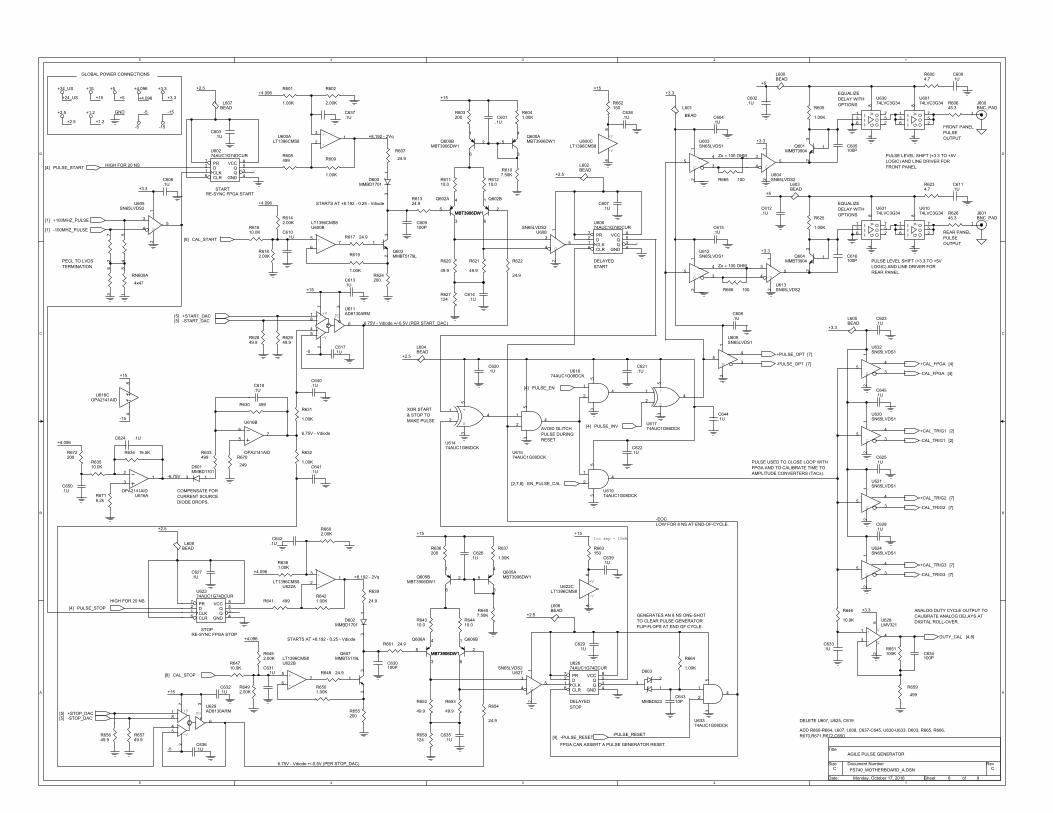
5
5
4
4
3
3
2
2
1
1
D D
C C
B B
A A
DELAYEDSTART
DELAYEDSTOP
RE-SYNC FPGA STOPSTOP
STARTRE-SYNC FPGA START
6.75V - Vdiode
FRONT PANELPULSEOUTPUT
PECL TO LVDSTERMINATION
+8.192 - 2Vq
STARTS AT +8.192 - 0.25 - Vdiode
6.75V - Vdiode +/-0.5V (PER START_DAC)
6.75V - Vdiode +/-0.5V (PER STOP_DAC)
STARTS AT +8.192 - 0.25 - Vdiode
+8.192 - 2Vq
GLOBAL POWER CONNECTIONS
-6.75V
PULSE USED TO CLOSE LOOP WITHFPGA AND TO CALIBRATE TIME TOAMPLITUDE CONVERTERS (TACs).
ANALOG DUTY CYCLE OUTPUT TOCALIBRATE ANALOG DELAYS ATDIGITAL ROLL-OVER.
PULSE LEVEL SHIFT (+3.3 TO +5VLOGIC) AND LINE DRIVER FORFRONT PANEL.
Zo = 100 OHM
DELETE U607, U625, C619
ADD R660-R664, L607, L608, C637-C645, U630-U633, D603, R665, R666,R670,R671,R672,C650
HIGH FOR 20 NS
HIGH FOR 20 NS
AVOID GLITCHPULSE DURINGRESET
XOR START& STOP TOMAKE PULSE
LOW FOR 8 NS AT END-OF-CYCLE.
EQUALIZEDELAY WITHOPTIONS
Zo = 100 OHM
REAR PANELPULSEOUTPUT
PULSE LEVEL SHIFT (+3.3 TO +5VLOGIC) AND LINE DRIVER FORREAR PANEL.
EQUALIZEDELAY WITHOPTIONS
FPGA CAN ASSERT A PULSE GENERATOR RESET.
COMPENSATE FORCURRENT SOURCEDIODE DROPS.
GENERATES AN 8 NS ONE-SHOTTO CLEAR PULSE GENERATORFLIP-FLOPS AT END OF CYCLE.
Icc amp = 10mA
FS740_MOTHERBOARD_A.DSN C
AGILE PULSE GENERATOR
C
6 9Monday, October 17, 2016
Title
Size Document Number Rev
Date: Sheet of
+4.096+15
+15
-5
+15
+15
+4.096
-5
-15
+15
+3.3
+2.5
+2.5
+1.2
+24_US
-15-5
+15 +5
-PULSE_RESET
+2.5
+2.5
+4.096
+4.096
+2.5
GND
+3.3
+3.3
+3.3
+3.3
-EOC
+3.3
+3.3
+5
+5
+15
+15+2.5
+4.096
+4.096
-15
+2.5
+3.3+24_US +15 +4.096
+1.2
+5
-5
R658124
Q600AMBT3906DW1
4
3
5
R63510.0K
R61210.0
C608.1U
Q605BMBT3906DW1
1
6
2
R632
1.00K
R672200
R6107.50K
C634100P
U60674AUC1G74DCUR
7216
8534
PRDCLKCLR
VCCQQ
GND
C626.1U
+
+
-
-
PD+V
-V
U611AD8130ARM1
8
45
62
7 3
Q602A
MBT3906DW1
4
3
5
R652
49.9
R62645.3
R62949.9
Q603MMBT5179L2
3
1
U61074LVC3G34
136
752
48
III
OOOG
V
R622
24.9
D601MMBD1701
13
C636.1U
R65749.9
R62849.9
C616100P
R625
1.00K
R646
10.0K
C627.1U
C625.1U
R634 16.5K
+
-
U622ALT1396CMS8
12
3
R655200
G
U620SN65LVDS1
54
3
12
R64310.0
C633.1U
G
U624SN65LVDS1
54
3
12
C631.1U
C602.1U
L606BEAD
R6602.00K
R6041.00K
C618.1U
C609100P
R639
24.9
R6492.00K
R636200
U616COPA2141AID
84
+
G
U61774AUC1G86DCK
41
2
53
+
G
U61474AUC1G86DCK
41
2
53
R665 100
U616B
OPA2141AID
5
67
G
U613SN65LVDS2
3
45
12
Q601MMBT3904
1
23
R6142.00K
U616AOPA2141AID
3
21
L600BEAD
L605BEAD
R653
49.9
C632.1U
C650.1U
R633499
R608499
U61574AUC1G08DCK
1
2
3
4
5
R61324.9
R648 24.9
C640.1U
C612.1U
C617.1U
C607.1U
C606.1U
R662150
L602BEAD
R64710.0K
R624200
R64410.0
U61874AUC1G08DCK
1
2
3
4
5
C628.1U
L608BEAD
C635.1U
R6004.7
R6381.00K
L607BEAD
C623.1U
+
- G
V
U628LMV321
1
3
2
4
5
U63074LVC3G34
136
752
48
III
OOOG
V
G
U612SN65LVDS1
54
3
12
C610.1U
U60174LVC3G34
136
752
48
III
OOOG
V
R6501.00K
R651100K
L601
BEAD
R666 100
-
+
U622BLT1396CMS8
76
5
R641 499
Q604MMBT3904
1
23
R627124
R60645.3
C64310P
R670
249
L604BEAD
R602
2.00K
R654
24.9
Q606A
MBT3906DW1
4
3
5
C621.1U
C615.1U
U63174LVC3G34
136
752
48
III
OOOG
V
Q602B
MBT3906DW1
1
6
2
G
U621SN65LVDS1
54
3
12
RN600A
4x47
18
C644.1U
C603.1U
36
G
U608SN65LVDS2
3
45
12
C637.1U
R663150
U63374AUC1G08DCK
1
2
3
4
5
R609
1.00K
J600BNC_PAD
1
R631
1.00K
27
R630 499
R6407.50K
+
-
U600ALT1396CMS8
12
3
+V
-V
U622CLT1396CMS8
84
C645.1U
R6452.00K
45
R620
49.9
R6716.2k
L603BEAD
C642.1U
R637
1.00K
+V
-V
U600CLT1396CMS8
84
R61610.0K
D602MMBD1701
13
U62674AUC1G74DCUR
7216
8534
PRDCLKCLR
VCCQQ
GND
G
U604SN65LVDS2
3
45
12
C630100P
+
+
-
-
PD+V
-V
U629AD8130ARM1
8
45
6
27 3
Q606B
MBT3906DW1
1
6
2
R605
1.00K
C641.1U
C639.1U
U62374AUC1G74DCUR
7216
8534
PRDCLKCLR
VCCQQ
GND
C629.1U
G
U603SN65LVDS1
54
3
12
C601.1U
U60274AUC1G74DCUR
7216
8534
PRDCLKCLR
VCCQQ
GND
R601
1.00K
-
+
U600BLT1396CMS8
76
5
C614.1U
C600.1U
R603200
J601BNC_PAD
1
R61110.0
Q607MMBT5179L
23
1
U61974AUC1G08DCK
1
2
3
4
5
R6182.00K
R621
49.9
Q605AMBT3906DW1
4
3
5
R6421.00K
R6234.7
R661 24.9
C638.1U
G
U632SN65LVDS1
54
3
12
R619
1.00K
R664
1.00K
C611.1U
C620.1U
C605100P
D600MMBD1701
13
G
U627SN65LVDS2
3
45
12
G
U609SN65LVDS1
54
3
12
G
U605SN65LVDS2
3
45
12
C613.1U
C624 .1U
R607
24.9
D603
MMBD523
31
2
C604.1U
R659
499
C622.1U
Q600BMBT3906DW1
1
6
2
R617 24.9
R65649.9
+START_DAC[5]-START_DAC[5]
+STOP_DAC[5]
PULSE_STOP[4]
-STOP_DAC[5]
PULSE_START[4]
CAL_START[8]
CAL_STOP[8]
+100MHZ_PULSE[1]
-100MHZ_PULSE[1]
-PULSE_RESET[4]
PULSE_INV[4]
PULSE_EN[4]
EN_PULSE_CAL[2,7,8]
+CAL_FPGA [4]
+CAL_TRIG2 [7]
-CAL_FPGA [4]
-CAL_TRIG2 [7]
-CAL_TRIG3 [7]
+CAL_TRIG3 [7]
DUTY_CAL [4,8]
+PULSE_OPT [7]
-PULSE_OPT [7]
+CAL_TRIG1 [2]
-CAL_TRIG1 [2]
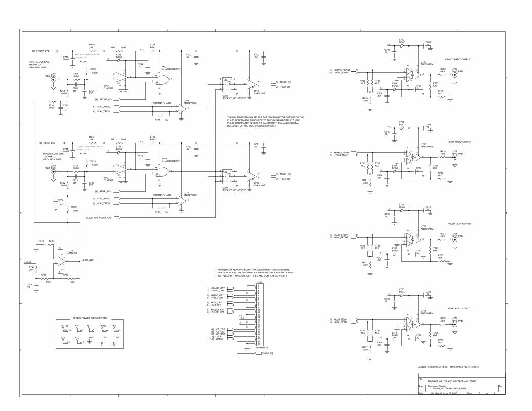
5
5
4
4
3
3
2
2
1
1
D D
C C
B B
A A
FRONT "FREQ" OUTPUT
FRONT "AUX" OUTPUT
REAR "FREQ" OUTPUT
TERMINATE LVDS
TERMINATE LVDS
HEADER FOR REAR PANEL (OPTIONAL) DISTRIBUTION AMPLIFIERS.VERTICAL PCB PLUGS INTO HEADER WHEN OPTIONS ARE INSTALLED.INSTALLED OPTIONS ARE IDENTIFIED AND CONFIGURED VIA SPI.
INPUTS LOOK LIKE1MOHM TOGROUND + 20PF.
INPUTS LOOK LIKE1MOHM TOGROUND + 20PF.
THE MULTIPLEXER CAN SELECT THE DISCRIMINATOR OUTPUT OR THEPULSE GENERATOR AS SOURCE TO TIME-TAGGING CIRCUITS. (THEPULSE GENERATOR IS USED TO CALIBRATE THE ANALOG/DIGITALROLLOVER OF THE TIME-TAGGING SYSTEM.)
REAR "AUX" OUTPUT
GLOBAL POWER CONNECTIONS
-4.096 VDC
ADDED R738,C726,C740,C741,R740,R739,C742,R741,C743
Avoid kick-back fromcomparator
Avoid kick-back fromcomparator
FS740_MOTHERBOARD_A.DSN C
TRIGGER INPUTS AND WAVEFORM OUTPUTS
C
7 9Monday, October 17, 2016
Title
Size Document Number Rev
Date: Sheet of
+5
+5+3.3
-5
-5
-5
-5
+5
+5
+4.096
+5
+3.3
+4.096+5
+5
-5
+1.2
+24_US
-15
+3.3
+2.5
-5
+15 +4.096
GND
+5
+5
-5
+3.3
+4.096
-15
+2.5
+3.3+24_US +15 +4.096
+1.2
+5
-5
C713.1U
R7041.00M
R730402
0
1
S G
V
U709SN74LVC1G3157DBVR
3
1
6 2
4
5
C721.1U
R72649.9
R741200
+
+
-
-
PD+V
-V
U700AD8130ARM
18
45
6
27 3
L701BEAD
R73724.9
C711.1U
R70349.9
+V
-V-EN
+
-
U701TLV3501
3
15
26
4
+
G
U70274LVC1G86DBVR
41
2
53
+
G
U70874LVC1G86DBVR
41
2
53
G
U704SN65LVDS1
54
3
12
R735499
G
U705SN65LVDS2
3
45
12
C725.1U
R713 100K
C743.1U
C723.1U
+
- G
V
U712LM321MF
1
3
2
4
5
C709.1U
C720.1U
J706
HEADER 25
12345678910111213141516171819202122232425
R740 49.9k
R707499
R736402
L706BEAD
R72549.9
R7381.00K
C712.1U
C702.1U
L709BEAD
J705BNC_PAD
1
R73124.9
J704BNC_PAD
1
R7191.00M
R73449.9
R73349.9
+
+
-
-
PD+V
-V
U713AD8130ARM
18
45
6
27 3
R7082.00M
C716.1U
R718499
L703BEAD
R71449.9
C71533P
R72449.9
R73249.9
+
+
-
-
PD+V
-V
U706AD8130ARM
18
45
6
27 3
J701BNC_PAD
1
R702
1.00M
R70649.9
C722.1U
C719.1U
R70549.9
0
1
S G
V
U703SN74LVC1G3157DBVR
3
1
6 2
4
5
R728
100K
J703BNC_PAD
1
C710.1U
R727499
J702BNC_PAD
1
C704.1U
R700249
C742
.1U L708BEAD
R720402
R71024.9
R739
1.00K
L711BEAD
C701.1U
J700BNC_PAD
1
R71649.9
C726
.1U
L705BEAD
R711 100
L702BEAD
R7222.00M
C7401000P
G
U710SN65LVDS1
54
3
12
C71727P
C708.1U
R712249
C724.1U
C703.1U
C700.1U
L704BEAD
R72124.9
R701 100K
R729
100K
C718.1U
+V
-V-EN
+
-
U707TLV3501
3
15
26
4
C70533P
G
U711SN65LVDS2
3
45
12
R709402
R715
1.00MC714.1U
C7411000P
C706.1U
R71749.9
L700BEAD
L707BEAD
L710BEAD
R723 100
+
+
-
-
PD+V
-V
U714AD8130ARM
18
45
6
27 3
C70727P
FRONT_POL[8]
FRONT_LVL[8]
+TRIG2 [3]
-TRIG2 [3]
+10MHZ_OPT[1]-10MHZ_OPT[1]
+FREQ_OPT[5]-FREQ_OPT[5]
-AUX_OPT[5]+AUX_OPT[5]
+PULSE_OPT[6]-PULSE_OPT[6]
-CS_TOP[8]-CS_MID[8]-CS_BOT[8]QSCK[1,8]QMOSI[1,8]
QMISO [8]
+CAL_TRIG2[6]
-CAL_TRIG2[6]
-FREQ_FRONT[5]
+AUX_FRONT[5]-AUX_FRONT[5]
+FREQ_FRONT[5]
+FREQ_REAR[5]-FREQ_REAR[5]
-TRIG3 [3]
+TRIG3 [3]
REAR_POL[8]
+CAL_TRIG3[6]
EN_PULSE_CAL[2,6,8]
-CAL_TRIG3[6]
REAR_LVL[8]
+AUX_REAR[5]-AUX_REAR[5]
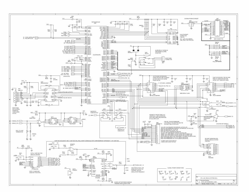
5
5
4
4
3
3
2
2
1
1
D D
C C
B B
A A
8MB SERIAL FLASH.
OCTAL 12-BIT DAC FORANALOG CONTROL.
-CS TO NOISY SPI DEVICES:THESE DEVICES ARE TOLERANTOF DATA AND CLOCK NOISEFROM THE SPI.
LINK: RIGHT LED (YELLOW)
RJ45 ETHERNETCONNECTOR(TAB UP)
REAR PANELRS-232 SERIALINTERFACE.CONFIGUREDAS DCE.
ACT: LEFT LED (GREEN)
UTXD0 & RTS0 ARE OUTPUTS
0 = SPI DWELL ADDRESS
QUIET SPI DEVICES: THE SCK ANDMOSI TO THESE DEVICES AREGATED "OFF" WHEN NOT USED.
EXTEND POWER-ON RESET
PULL-UP FOR SPI
HEADER TO FRONT PANEL GUI(GRAPHICAL USER INTERFACE).KEYS AND LAMPS ARE SERVICEDBY GUI's MPU's SPI.
SHARE UART BETWEEN RUBIDIUMTIMEBASE AND GUI BOOTLOAD.
RI
ISOLATES QMISOFROM NOISYMISO.
DTR
NOTE: LTC2620 SDODOES NOT TRI-STATE.
BDM CONNECTOR
COLDFIRE MPU.
URXD0 & CTS0 ARE INPUTS
12-BIT DAC SCALED BY 1000:1 12-BIT DAC WILL ROLL-OVER TO MIDSCALE WITH CARRY/BORROW TO/FROM BIT 11 OF 16-BIT DAC.
HIGH RESOLUTION, LOWNOISE DAC OUTPUT TOCONTROL CRYSTALOSCILLATOR FREQUENCY.
ALARM RELAY SHOWN INUNPOWERED (ALARM)CONDITION.
REAR PANELCONNECTOR
(DUPLICATE)
UART FOR GPS RECEIVER.
UN-GATED SPI SIGNALS.
-GUI_RFS: GUI REQUEST FOR SERVICE, ACTIVE LOW-MB_RFS: MOTHERBOARD REQUEST FOR SERVICE, ACTIVE LOWMOSI: SPI MASTER OUT, SLAVE IN.
SCK: SPI CLOCK, SOURCED BY MASTER-CS_GUI: SPI "CHIP SELECT" FOR GUI, ACTIVE LOW.-RESET_GUI: OPEN DRAIN, PULLED LOW BY MB TO RESET GUI.-RESET_MB: OPEN DRAIN, PULLED LOW BY GUI TO RESET MB.-BOOTLOAD_GUI: HELD LOW THRU RESET TO FORCE GUI BOOTLOAD.MIGO: MOTHERBOARD IN, GUI OUT (BOOTLOAD DATA)
MISO: SPI MASTER IN, SLAVE OUT.
MOGI: MOTHERBOARD OUT, GUI IN (BOOTLOAD DATA)
+10 MHZ LVDS CLOCK FOR GUI-10MHZ LVDS CLOCK FOR GUI
FOR SPI, THE MOTHERBOARD(COLDFIRE) IS THE MASTER AND THEGUI (NXP1788) IS THE SLAVE.
MASTER INRUBIDIUM OUT.
MASTER OUTRUBIDIUM IN.
(CPU,53)
CONFIGURE AS ANINPUT TO DE-ASSERT
PECL TO LVDSTERMINATION
GLOBAL POWER CONNECTIONS
SPI SHIFT REGISTER FORMISCELLANEOUS SYSTEMCONTROL.
FS740_MOTHERBOARD_A.DSN C
CPU, LAN, RS232 & SYSTEM DACs
C
8 9Monday, October 17, 2016
Title
Size Document Number Rev
Date: Sheet of
RTS
MISO
TMS/BKPTTCLK
-ACT_LED
+5
-EN_SPI
MISO
DSR
TMS/BKPT
PST0
-CS_DAC12
-MB_RFS
ALLPST
-LINK_LED
ALLPST
+3.3
RX
+4.096
-CS_DAC12
-CS_FLASH
+3.3
TDI/DSI
CD
-TRST
MOSI
DDATA2
PST1
-GUI_RFS
-CS_GUI
TDO/DSO
DDATA3
QSCK
-TRST
QSCK
PST0
SCK
+3.3
-TRST
PULLDWN
PST1
-CS_DAC16
TX
+3.3
PST2
PST3
+3.3
TDO/DSO
QMOSI
DDATA3
-RESET_MB
PST2
CTS
TCLK
+3.3
DDATA0
SCK
+3.3
DDATA1
QMOSI
MOSI
+3.3
+3.3
+3.3
25MHZ
+3.3
MISO
+3.3
DDATA0DDATA2
+3.3
DDATA1
TDI/DSI
PST3
+3.3
25MHZ
+15
-15
QSCK-CS_DAC16
QMOSIQMISO
-RESET
+15
+8.192
+3.3
+5_FP
-GUI_RFS-MB_RFSMOSIMISO
-CS_GUI
-RESET_MB-RESET_GUI
-BOOTLOAD_GUI
SCK
+RB/-BL
MOGIMIGO
+3.3
-BOOTLOAD_GUI
+1.2
+24_US
-15
+3.3
+2.5
-5
+15 +4.096
GND
+5
+3.3 -RESET_MB
+3.3
-CS_MISC
+5
-ALARM
TDO/DSOTDI/DSI
PULLDWN
TMS/BKPT
-RESET_MB-RESET
+3.3
+5_FP
+4.096
-15
+2.5
+3.3+24_US +15 +4.096
+1.2
+5
-5
+5_FP
0
1
S G
V
U809SN74LVC1G3157DBVR
3
1
6 2
4
5
J803HEADER 16
12345678910111213141516
45
RN800A
4x47
18
C801.1U
0
1
SG
V
U810SN74LVC1G3157DBVR
3
1
62
4
5
36
U81174LVC1G125
24
1 35
3 6
27
C824.1U
RN803A4x47
18
C805.22U
45
C803.22U
L803BEAD
U81574LVC1G04
42
53
R811 100
L800BEAD
C816 .1U
U81374LVC1G74
7216
8534
PRDCLKCLR
VCCQQ
GNDG
U814SN65LVDS2
3
45
12
3 6
U812
74LVC1G74
7216
8534
PRDCLKCLR
VCCQQ
GND
C800.22U
L806BEAD
V
G U80874LVC2G08DCT
1
2
3
4
5
6
7
8
2 7
C802.1U
R80910.0K
J804RJ45_J1011F21PNL
127
36
8
12
1110
9
45
13141516
+TX-TX+RX
TXCTRXCT
-RX
+LEDL
-LEDL-LEDR
+LEDR
GNDGND
GNDGNDGNDGND
C812.1U
C830 .01U
RN801A4x10K
1 8
R841 100
C820 .1U
C822.1U
U80574LVC138APWR
8
15141312111097
123
546
16G
ND
Y0Y1Y2Y3Y4Y5Y6Y7
ABC
G2BG2AG1
VC
C
C814.1U
36
R8132.00K
J800CONN13x2
13579
1113151719212325
2468101214161820222426
U803HS-212
1 8
32
4
67
5
R802100
J801CON3123
C826.1U
4 5
C818100P
L808BEAD
R80012.1K
R8071.00K
L802BEAD
U806M25PE80VMN6TP
12 3
4
56
78
CSSDO WR
GND
SDISCK
RSTVCCR808
10.0K
TP800TEST POINT
1
U819AD5760
2
16
1
20
24
3
171825
89
19
15
10 21 22 23
14131211
7
6
4
5VRH
VRL
VOUT
RFB
INV
VDD
VSSVSSPAD
VCCVIO
AGND
DGND
NC
NC
NC
NC
-SYNCSCLKSDINSDO
-LDAC
-CLR
-RESET
VDD
TP801TEST POINT
1
+
-
U817AOP284FS
12
3
-
+
U817BOP284FS
76
5
L801BEAD
C806.22U
+V
-V
U817COP284FS8
4
C819.1U
27
C825.1U
U81674HC595A
16141110
15123456798
1312
VCCSICLKCLR
Q0Q1Q2Q3Q4Q5Q6Q7SOGND
OERCK
C823.1U
RN802A4x10K
1 8
R8142.00K
U818LTC2620CGN
16
6
117891
23451213141510
VCC
REF
CLRCSSCKSDIGND
VAVBVCVDVEVFVGVH
SDO
L807BEAD
U80474LVC138APWR
8
15141312111097
123
546
16G
ND
Y0Y1Y2Y3Y4Y5Y6Y7
ABC
G2BG2AG1
VC
C
R818
2.00K
C810.22U
D800BAW56LT1
3
12
C817100P
R816
1.00M
R815100
R801100
C8114.7U/50V
4 5
C815 .1U
R803100K
L809BEAD
R8401.00K
C813.1U
R804100K
R810 100
C804.22U
U807ADM3202ARUZ
3116
1011
912
1545
138
6
147
2 C1-C1+VCC
DINDIN
ROUTROUT
GNDC2+C2-
RINRIN
V-
DOUTDOUT
V+
C828.1U
L804
BEAD
J802DB9F318
594837261
1011
C807.22U
Q800MMBT3904
23
1
U800DS1816R-20/T&R
12
3
RSTV
G
MCF52235CAL60U801
1011
12131617
18
19
606162
63
77787980
9798
99100103104
105106
56
55545341
403938
44
50
7654321
89
20
21
112111
22
2324
2526
2728
29
30
31
32
33
343536
37
84838159585251
85868788
89909192
110109108107
7473717066
7569
68
767267
93
1443
65102
82
46
45
47
94
9596
15
64101
4849
57
42
IRQ8*IRQ9*
DDATA3DDATA2DDATA1DDATA0
JTAG_EN
IRQ6*
URTS2UCTS2URXD2
UTXD2
PST0PST1PST2PST3
IRQ12*IRQ13*
PWM1/PTD0PWM3/PTD1PWM5/PTD2PWM7/PTD3
IRQ14*IRQ15*
IRQ7*
IRQ1*IRQ2*IRQ3*IRQ4*
SPI_CS3SPI_CS2SPI_CS1
RSTI*
TEST
ALLPSTTRST*
TDO/DSOTDI/DSIRCON*
TMS/BKPTTCLK
TIN0TIN1
IRQ5*
TIN2
I2C_SDAI2C_SCL
TIN3
RTS1CTS1
RTS0CTS0
SYNCBSYNCA
IRQ10*
URXD0
UTXD0
URXD1
UTXD1
SPI_DINSPI_OUTSPI_SCK
SPI_CS0
ACT_LEDLNK_LEDSPD_LEDDUP_LEDCOL_LED
RXLEDTXLED
AN4AN5AN6AN7
AN3AN2AN1AN0
GPT0GPT1GPT2GPT3
PHY_RXNPHY_RXPPHY_TXNPHY_TXP
PHY_RBIAS
PHY_VDDRXPHY_VDDTX
PHY_VDDA
PHY_VSSRXPHY_VSSTX
PHY_VSSA
VDDA
VDDX1VDDX2
VDD2VDD1
VDDR
RST0*
VDDPLL
VSSPLL
VRH
VRLVSSA
VSSX1
VSS2VSS1
EXTALXTAL
IRQ11*
VSSX2
R8172.00K
2 7
C827 .01U
C821
.1U
C809 .22U
QMOSI [1,7]
QMISO [7]
-CS_FPGA [4]
-PWR_IRQ[9]
MOSI [4]MISO [4]
INIT_B[4]DONE[4]
PS_SYNC [9]
SCK [4]
QSCK [1,7]
-RST/PROG_FPGA [4]
MORI [1]
MIRO[1]
-100MHZ_CPU[1]
+100MHZ_CPU[1]
-RB_INSTALLED[1]-OCXO_INSTALLED[1]
-CS_100MHZ [1]
XTAL_HEAT[1]
DUTY_CAL[4,6]
100MHZ_LOCK[1]EFC_100MHZ[1]EFC_10MHZ[1]
XTAL_TEMP[1]
ANT_MON[2]
MOTI [2]
MITO [2]
-GPS_RESET [2]
EN_100MHZ[1]
BOOT_M0[4]BOOT_M1[4]BOOT_M2[4]
DAC_SLEEP[5]EN_PULSE_CAL[2,6,7]
DAC/-PLL[1]
AUX/-100MHZ[5]
TEMP_CTL [1]CAL_START [6]CAL_STOP [6]FRONT_LVL [7]REAR_LVL [7]
AUX_AMPL [5]FREQ_AMPL [5]
-10MHZ_GUI[1]+10MHZ_GUI[1]
-CS_TOP [7]-CS_MID [7]-CS_BOT [7]
FRONT_POL[7]REAR_POL[7]
-ANT_OC[2]
BIG_DAC [1]
PWM_FPGA [4]
-RESET_MB[9]
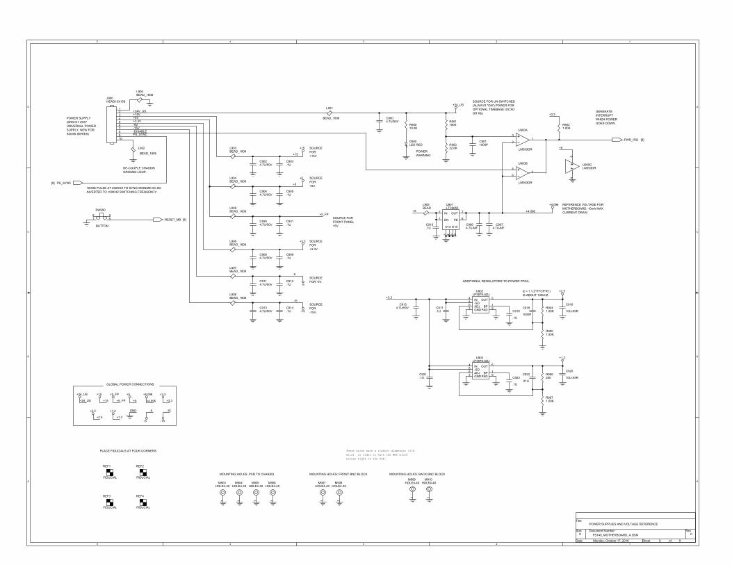
5
5
4
4
3
3
2
2
1
1
D D
C C
B B
A A
SOURCEFOR+15V.
PLACE FIDUCIALS AT FOUR CORNERS
POWERWARNING
GENERATEINTERRUPTWHEN POWERGOES DOWN.
MOUNTING HOLES: PCB TO CHASSIS
SOURCEFOR+5V.
100NS PULSE AT 200KHZ TO SYNCHRONIZE DC-DCINVERTER TO 100KHZ SWITCHING FREQUENCY.
SOURCEFOR+3.3V.
SOURCE FOR UN-SWITCHED(ALWAYS "ON") POWER FOROPTIONAL TIMEBASE (OCXOOR Rb)
SOURCEFOR -5V.
SOURCEFOR-15V.
fz = 1 / (2*PI*Cff*R1)IS ABOUT 100kHZ.
POWER SUPPLY(SRS KIT #337UNIVERSAL POWERSUPPLY, NEW FORSG385 SERIES)
DE-COUPLE CHASSISGROUND LOOP.
REFERENCE VOLTAGE FORMOTHERBOARD. 10mA MAXCURRENT DRAW.
GLOBAL POWER CONNECTIONS
ADDITIONAL REGULATORS TO POWER FPGA.
MOUNTING HOLES: FRONT BNC BLOCK MOUNTING HOLES: BACK BNC BLOCK
These holes have a tighter diamenter (118mils) in order to have the BNC blocksecure tight ot the PCB.
SOURCE FORFRONT PANEL+5V.
FS740_MOTHERBOARD_A.DSN C
POWER SUPPLIES AND VOLTAGE REFERENCE
C
9 9Monday, October 17, 2016
Title
Size Document Number Rev
Date: Sheet of
+5
+15
PS_SYNC
+3.3
+5
-5V
+5V
-15
-DISABLE
+15V
+3.3V
+24V_US
+3.3
-15V
+5
+1.2
+24_US
-15
+3.3
+2.5
+15 +4.096+5
+4.096
-5
-5GND
+5_FP
+5_FP
+5
+3.3
+1.2
+15
-5
+24_US
-15
+2.5
+4.096
-15
+2.5
+3.3+24_US +15 +4.096
+1.2
+5
-5
+5_FP
C9011000P
L902
BEAD_1806
C9154.7U/50V
M907HOLE4-40
1
L904BEAD_1806
C9114.7U/50V
U901LTC6655
2
1
7
6
3 4 5 8
IN
EN
OUT
FB
G G G G
R9051.00K
M904HOLE4-40
1
C9074.7U-MF
M908HOLE4-40
1
L909BEAD_1806
C917.1U
R90010.0K
C914.1U
C9304.7U/50V
C931.1U
L900BEAD_1806
R906200
U903LP3878-ADJ
13
4 5
68
9BPGND
IN OUT
ADJ-SD
PAD
C919
.1U
C9084.7U/50V
M905HOLE4-40
1
M910HOLE4-40
1
C921.1U
L901
BEAD_1806
C9134.7U/50V
SW900
BUTTON
12 3
4.. .
.
M909HOLE4-40
1
U900B
LM393DR
5
67
C903.1U
L907BEAD_1806
C918
1000P
J900HEAD10X156
12345678910
REF4
FIDUCIAL
M903HOLE4-40
1
C922
.01U
R9021.00K
R901100K
L905BEAD
C9004.7U/50V
L903BEAD_1806
M906HOLE4-40
1
D900LED RED
C916
10U-X5R
REF2
FIDUCIAL
C910.1U
U900CLM393DR
84
C912.1U
L906BEAD_1806
R90322.6K
U902LP3878-ADJ
13
4 5
68
9BPGND
IN OUT
ADJ-SD
PAD
C9064.7U-MF
L908BEAD_1806
C9024.7U/50V
C923
.1U
R9071.00K
C909.1U
R9041.50K
REF1
FIDUCIAL
C905.1U
U900A
LM393DR
3
21
C920
10U-X5R
REF3
FIDUCIAL
C9044.7U/50V
-PWR_IRQ [8]
PS_SYNC[8]
-RESET_MB [8]
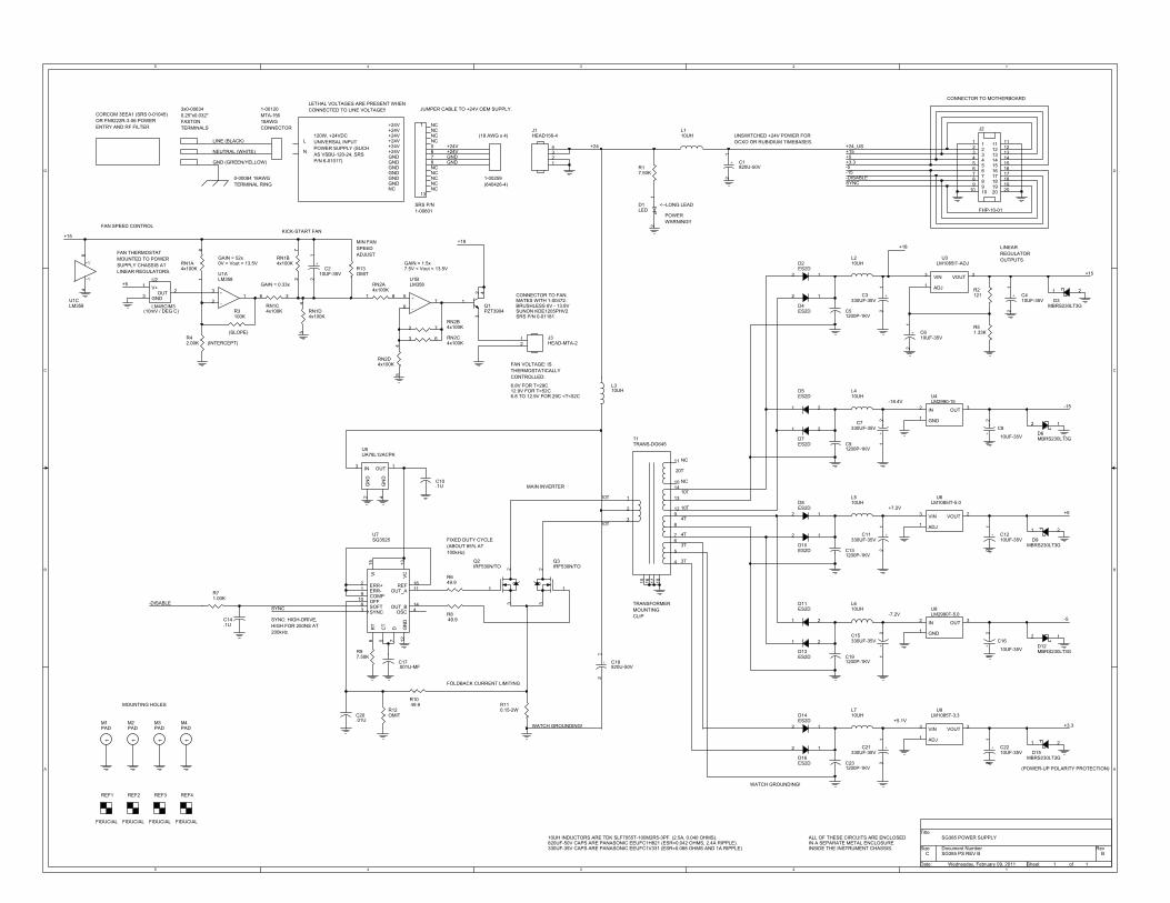
5
5
4
4
3
3
2
2
1
1
D D
C C
B B
A A
10T
10T
10T
10T
3T
3T
4T
4T
20T
NC
NC
-18.4V
+7.2V
-7.2V
+5.1V
CONNECTOR TO FAN.
BRUSHLESS 6V - 13.8VSUNON KDE1205PHV2SRS P/N 0-01181
FAN THERMOSTATMOUNTED TO POWERSUPPLY CHASSIS ATLINEAR REGULATORS.
(10mV / DEG C)
FAN VOLTAGE: ISTHERMOSTATICALLYCONTROLLED:
6.8V FOR T<29C12.9V FOR T>52C6.8 TO 12.9V FOR 29C <T<52C
GAIN = 52x0V < Vout < 13.5V GAIN = 1.5x
7.5V < Vout < 13.5V
KICK-START FAN
ALL OF THESE CIRCUITS ARE ENCLOSEDIN A SEPARATE METAL ENCLOSUREINSIDE THE INSTRUMENT CHASSIS.
(INTERCEPT)
(SLOPE)
120W, +24VDCUNIVERSAL INPUTPOWER SUPPLY (SUCHAS VSBU-120-24, SRSP/N 6-01017)
LETHAL VOLTAGES ARE PRESENT WHENCONNECTED TO LINE VOLTAGE!!
POWERWARNING!!
10UH INDUCTORS ARE TDK SLF7055T-100M2R5-3PF. (2.5A, 0.040 OHMS).820UF-50V CAPS ARE PANASONIC EEUFC1H821 (ESR=0.042 OHMS, 2.4A RIPPLE).330UF-35V CAPS ARE PANASONIC EEUFC1V331 (ESR=0.068 OHMS AND 1A RIPPLE)
(POWER-UP POLARITY PROTECTION)
FOLDBACK CURRENT LIMITING
SYNC: HIGH-DRIVE,HIGH FOR 250NS AT200kHz.
UNSWITCHED +24V POWER FOROCXO OR RUBIDIUM TIMEBASES.
FIXED DUTY CYCLE(ABOUT 85% AT100kHz)
WATCH GROUNDING!
WATCH GROUNDING!
JUMPER CABLE TO +24V OEM SUPPLY.
MATES WITH 1-00472.
<--LONG LEADSRS P/N1-00601
1-00259(640426-4)
(18 AWG x 4)+24V+24V+24VGNDGNDGND
CORCOM 3EEA1 (SRS 0-01045)OR FN9222R-3-06 POWERENTRY AND RF FILTER
3x0-006340.25"x0.032"FASTONTERMINALS
LINE (BLACK)
NEUTRAL (WHITE)
GND (GREEN/YELLOW)
+24V+24VGNDGND
NC
NC
L
N
1-00120MTA-15618AWGCONNECTOR
0-00084 18AWGTERMINAL RING
FAN SPEED CONTROL
MAIN INVERTER
LINEARREGULATOROUTPUTS
CONNECTOR TO MOTHERBOARD
MOUNTING HOLES
NC
NC
MIN FANSPEEDADJUST
TRANSFORMERMOUNTINGCLIP
GAIN = 0.33x
NCNC
NC
NCNC
1
13
5678
+24V+24V+24V
GND
GNDGND
NC
SG385 PS REV B B
SG385 POWER SUPPLY
C
1 1Wednesday, February 09, 2011
Title
Size Document Number Rev
Date: Sheet of
+3.3
-5
+5
-15
+24_US+15+5+3.3
+24
+5
SYNC-DISABLE
+18+18
+15
+15
SYNC-DISABLE-15-5
+ C1210UF-35V
12
D16ES2D
2 1
D3MBRS230LT3G
21
L310UH
RN1C4x100K
36
L610UH
D1LED
12
C131200P-1KV
REF4
FIDUCIAL
T1TRANS-DG645
1
2
3
4
5
67
8
9
10
11
12
13
14
15 16 17 18
D12MBRS230LT3G
2 1
RN2A4x100K
1 8
M2PAD
1
D9MBRS230LT3G
21
R3100K
+C2
10UF-35V
12
+C11330UF-35V
12
C51200P-1KV
R849.9
D8ES2D
2 1
+C3330UF-35V
12
C10.1U
D4ES2D
2 1
C191200P-1KV
Q3IRF530N/TO2
1
3
C14.1U
+
-
U1ALM358
12
3
D15MBRS230LT3G
21
Q1PZT3904
1
23
4
+
C15330UF-35V
12
L710UH
+
C7330UF-35V
12
D13ES2D
21
U4LM2990-15
1
32
GND
OUTIN
RN2B4x100K2 7
M3PAD
1
RN1A4x100K
18
R649.9
R71.00K
J3HEAD-MTA-2
12
U6LM1085IT-5.0
3
1
2VIN
ADJ
VOUT
+ C2210UF-35V
12
U2
LM45CIM3
1
32V+
GNDOUT
M1PAD
1
J2
FHP-10-01
123456789
10
11121314151617181920
12345678910
11121314151617181920
D10ES2D
2 1
U9LM1085T-3.3
3
1
2VIN
ADJ
VOUT
REF1
FIDUCIAL
R97.50K
R12OMIT
D2ES2D
2 1
L410UH
-
+
U1BLM358
76
5
L510UH
U7SG3525
12
3 4
56 7
8
910
11
1213
14
15
16ERR-ERR+
SYNC OSC
CT
RT
D
SOFT
COMPOFF
OUT_A
GN
DV
C
OUT_B
VI
REF
+ C1820U-50V
12
D11ES2D
21
+ C410UF-35V
12
C91200P-1KV
M4PAD
1
REF2
FIDUCIAL
+ C610UF-35V
12
+ C16
10UF-35V
12
D14ES2D
2 1
+C21330UF-35V
12
RN2D4x100K
45
R2121
RN2C4x100K
3 6
D7ES2D
21
RN1D4x100K
45
U3LM1085IT-ADJ
3
1
2VIN
ADJ
VOUT
R110.15-2W
R1049.9
RN1B4x100K
27
+ C8
10UF-35V
12
U8LM2990T-5.0
1
32
GND
OUTIN
C20.01U
+V
-V
U1CLM358
84
Q2IRF530N/TO 2
1
3
L110UH
U5UA78L12ACPK
3 1
2 4
IN OUT
GN
D
GN
D
J1HEAD156-4
1234
D6MBRS230LT3G
2 1
C17.001U-MF
R13OMIT
REF3
FIDUCIAL
D5ES2D
21
R42.00K
+ C18820U-50V
12
C231200P-1KV
R51.33K
L210UH
R17.50K
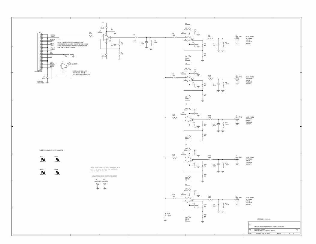
5
5
4
4
3
3
2
2
1
1
D D
C C
B B
A A
REAR PANELOPTIONAL10MHZTIMEBASEOUTPUT.
NON-INVERTED DATAINDICATES 10MHZDISTRIBUTION AMPLIFIER.
ISOLATEGROUNDS
EACH 10 MHZ DISTRIBUTION AMPLIFIERCONNECTS ITS GROUND PLANE TO THE -10MHZINPUT, ESTABLISHING A GROUND REFERENCEFOR THE FLOATING SIGNAL.
-10MHZ
REAR PANELOPTIONAL10MHZTIMEBASEOUTPUT.
REAR PANELOPTIONAL10MHZTIMEBASEOUTPUT.
REAR PANELOPTIONAL10MHZTIMEBASEOUTPUT.
REAR PANELOPTIONAL10MHZTIMEBASEOUTPUT.
ADDED C19 AND L19.
PLACE FIDUCIALS AT FOUR CORNERS
MOUNTING HOLES: FRONT BNC BLOCK
These holes have a tighter diamenter (118mils) in order to have the BNC blocksecure tight ot the PCB.
GPS OPTIONAL 10MHZ OUTPUTS A
GPS OPTIONAL REAR PANEL 10MHZ OUTPUTS
C
1 1Tuesday, July 15, 2014
Title
Size Document Number Rev
Date: Sheet of
+FREQ-FREQ
+AUX-AUX
+PULSE-PULSE
+5
-5
-CS
MISOMOSISCLK
+3.3
+5
+10MHZ
+5
-5-5
+5
-5
-5
+5
+5
-5
+5
-5
M1HOLE4-40
1
R25432
L18BEAD
L11.33UH
J2BNC_PAD
1
U374LVC1G125DBV
2 413
5
C9750P
R2
24.9
C6.1U
R6432
C8
.1U
L15BEAD
R910.0
M2HOLE4-40
1
R1049.9
+
-
+V
-VFB
U5AD8000
3
26
74
1
C3
.1U
R19432
R5432
L2BEAD
R2110.0
R8432
L6BEAD
C4
.1U
C18750P
C7.1U
J4BNC_PAD
1
R449.9
R24
24.9
R1449.9
C12750P
L5BEAD
R20432
C17
.1U
C5750P
L9BEAD
C1.1U
+
-
+V
-VFB
U1AD8000
3
26
74
1
L3.33UH
R15432
R1849.9
+
-
+V
-VFB
U2AD8000
3
26
74
1
R1310.0
+
-
+V
-VFB
U6AD8000
3
26
74
1
R7432
J3BNC_PAD
1
L8.33UH
C11
.1U
REF4
FIDUCIAL
R2249.9
C2.1U
R16432
R110.0
JP1
HEADER 25
123456789
10111213141516171819202122232425
C14
.1U
REF2
FIDUCIAL
L7BEAD
R11432
L10BEAD
R310.0
C15750P
L1BEAD
L16BEAD
+
-
+V
-VFB
U4AD8000
3
26
74
1
+
-
+V
-VFB
U7AD8000
3
26
74
1
J5BNC_PAD
1
C10.1U
R1710.0
L14.33UH
L4BEAD
R23432
C19750P
C16.1U
C13.1U
REF1
FIDUCIAL
R12432
L12BEAD
L13BEAD
J1BNC_PAD
1
L19.33UH
REF3
FIDUCIAL
L17.33UH
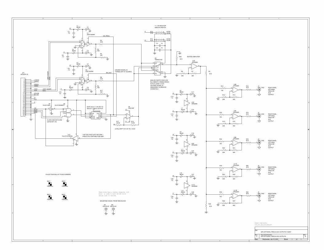
5
5
4
4
3
3
2
2
1
1
D D
C C
B B
A A
REAR PANELOPTIONALFREQ ORAUXOUTPUT.
REAR PANELOPTIONALFREQ ORAUXOUTPUT.
REAR PANELOPTIONALFREQ ORAUXOUTPUT.
REAR PANELOPTIONALFREQ ORAUXOUTPUT.
REAR PANELOPTIONALFREQ ORAUXOUTPUT.
VERY SHORTRUN
VE
RY
SH
OR
TR
UN
1-BIT DELAYED DATA RETURN =FREQ & AUX DISTRIBUTION AMP.
+/- 2.5V BIAS FORANALOG SWITCH
LEVEL SHIFT 0/+3.3V TO -/+2.5V
SHIFT IN A "1" VIA SPI TOSELECT "FREQ" OUTPUT.
ANALOG SWITCH HAS LOWRon (ABOUT 5 OHMS) WHICHIS FLAT OVER +/-2.5V.UN-USED SIGNAL ISGROUNDED TO REDUCECROSSTALK.
BUFFER AMPLIFIER
UNUSED SIGNAL ISTURNED OFF AT SOURCE.
CLOCK AND DATA AREGATED BY -CS.
These holes have a tighter diamenter (118mils) in order to have the BNC blocksecure tight ot the PCB.
PLACE FIDUCIALS AT FOUR CORNERS
MOUNTING HOLES: FRONT BNC BLOCK
Added components:R30,R31,R32,R33,R34,R35
GPS OPTIONAL FREQ & AUX OUTPUTS B
GPS OPTIONAL FREQ & AUX OUTPUTS 7-02467
C
1 1Wednesday, July 15, 2015
Title
Size Document Number Rev
Date: Sheet of
-FREQ
+5
-5
-CS
+3.3
-10MHZ+10MHZ
-PULSE+PULSE +5
-5
+5
-AUX+AUX
+FREQ
MISO
SCLKMOSI
EN_AUX
EN_FREQ
+5
-5
-5
+5
+5
-5
-5
+5
+5
+5
-5
-5
M1HOLE4-40
1
R249.9
C20.1U
C5.1U
C27.1U
R1049.9
R6
499
-
+
U9AOPA2695
82
1
R20
499
L4BEAD
R9499
M2HOLE4-40
1
C14.1U
U574LVC1G04
42
53
L2BEAD
J2BNC_PAD
1
U774LVC1G74
7216
8534
PRDCLKCLR
VCCQQ
GND
R31
100
R2549.9
J1BNC_PAD
1
R32
100
C23.1U
R24
499
C30.1U
R13
499
C9.1U
V
G
U674LVC2G08DCT
1
2
3
4
5
6
7
8
+V
-V
U11COPA2695
67
J5BNC_PAD
1
R33
100
L1BEAD C1
.1U
R34
100
C10.1U
R30
49.9
R5
49.9
+
-
U11BOPA2695
53
4
R35
100
R11402
R26
499
R15
499
R3499
L14BEAD
+V
-V
U3COPA2695
67
R849.9
R28
49.9
L11BEAD
L7BEAD
C19.1UU10
74LVC1G125DBV24
1 35
REF4
FIDUCIAL
R7
499
C3 .1U
R21
499
C7.1U
C28.1U
+
+
-
-
PD+V
-V
U4AD8130ARM
18
45
62
7 3
L3BEAD
-
+
U11AOPA2695
82
1
JP1HEADER 25
123456789
10111213141516171819202122232425
J4BNC_PAD
1
C24.1U
C8.1U
C2.1U
REF2
FIDUCIAL
+V
-V
U9COPA2695
67
J3BNC_PAD
1
R1449.9
G
V
0
01
1
U2TS5A623157
1
2
34
5
67
8
910
C29.1U
R23
499
R12
499
R1720.0K
R1A 4X10K1 8
R1810.0K
C6.1U
R1B 4X10K2 7
L6BEAD
+
- G
V
U8LM321MF
1
3
2
4
5
R1C 4X10K3 6
+
-
U9BOPA2695
53
4
R1D 4X10K4 5+
+
-
-
PD+V
-V
U1AD8130ARM
18
45
6
27 3
+
-
U3BOPA2695
53
4
C15.1U
R1949.9
R27
499
REF1
FIDUCIAL
R16
499
-
+
U3AOPA2695
82
1
R4402
C16.1U
C11.1U
L13BEAD
L9BEAD
C4 .1U
REF3
FIDUCIAL
R2249.9
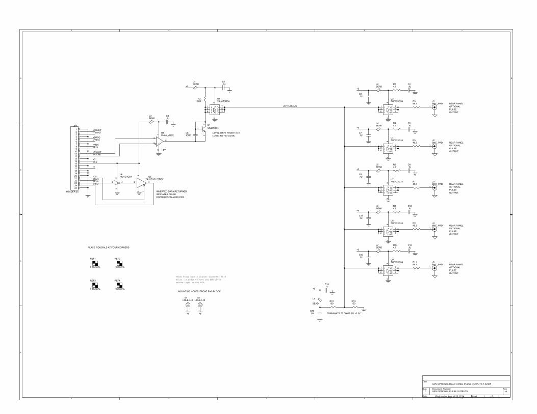
5
5
4
4
3
3
2
2
1
1
D D
C C
B B
A A
REAR PANELOPTIONALPULSEOUTPUT.
REAR PANELOPTIONALPULSEOUTPUT.
REAR PANELOPTIONALPULSEOUTPUT.
REAR PANELOPTIONALPULSEOUTPUT.
REAR PANELOPTIONALPULSEOUTPUT.
TERMINATE 75 OHMS TO +2.5V
INVERTED DATA RETURNEDINDICATES PULSEDISTRIBUTION AMPLIFIER.
+.8V
LEVEL SHIFT FROM +3.3VLOGIC TO +5V LOGIC
Zo=75 OHMS
MOUNTING HOLES: FRONT BNC BLOCK
These holes have a tighter diamenter (118mils) in order to have the BNC blocksecure tight ot the PCB.
PLACE FIDUCIALS AT FOUR CORNERS
GPS OPTIONAL PULSE OUTPUTS A
GPS OPTIONAL REAR PANEL PULSE OUTPUTS 7-02465
C
1 1Wednesday, August 20, 2014
Title
Size Document Number Rev
Date: Sheet of
+FREQ-FREQ
+AUX-AUX
+5
-5
-CS
MOSIMISO
SCLK
-10MHZ+10MHZ
+5+5
+5
+5
+5
+5
+5
+3.3
+PULSE-PULSE
R345.3
M1HOLE4-40
1
U574LVC1G125DBV
2 4
135
U174LVC3G34
136
752
48
III
OOOG
V
C15.1U
R12150
U474LVC3G34
136
752
48
III
OOOG
V
L2BEAD
M2HOLE4-40
1
R945.3
C9.1U
R14.7
J3BNC_PAD
1
C3.1U
U774LVC3G34
136
752
48
III
OOOG
V
C7.1U
L1BEAD
R1145.3
L7BEAD
R64.7
L5BEAD
C11.1U
J2BNC_PAD
1
R13150
U874LVC3G34
136
752
48
III
OOOG
V
C14.1U
R84.7
C1.1U
R21.00K
C4.1U
J4BNC_PAD
1
REF4
FIDUCIAL
R104.7
U974LVC3G34
136
752
48
III
OOOG
V
L3BEAD
C6100P
JP1
HEADER 25
123456789
10111213141516171819202122232425
REF2
FIDUCIAL
C10.1U
R44.7
C12.1U
R545.3
L8
BEAD
C2.1U
L6BEAD
U674LVC1G04
42
53
L4BEAD
J5BNC_PAD
1
C8.1U
REF1
FIDUCIAL
Q1MMBT3904
32
1
C13.1U
R745.3
U274LVC3G34
136
752
48
III
OOOG
V
J1BNC_PAD
1
G
U3SN65LVDS2
3
45
12
C5.1U
REF3
FIDUCIAL
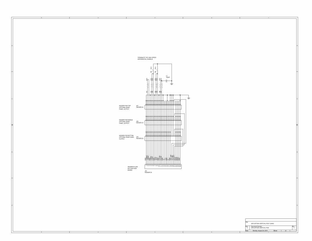
5
5
4
4
3
3
2
2
1
1
D D
C C
B B
A A
HEADER PLUGSINTO MOTHERBOARD.
HEADER FOR TOPOPTIONAL REARPANEL OUTPUT.
HEADER FOR MIDDLEOPTIONAL REARPANEL OUTPUT.
HEADER FOR BOTTOMOPTIONAL REAR PANELOUTPUT.
TERMINATE THE HIGH SPEEDDIFFERENTIAL SIGNALS.
GPS OPTION VERTICAL PCB C
GPS OPTION VERTICAL PCB 7-02483
C
1 1Monday, August 24, 2015
Title
Size Document Number Rev
Date: Sheet of
GN
D+1
0MH
Z-1
0MH
ZG
ND
+FR
EQ
-FR
EQ
GN
D+A
UX
-AU
XG
ND
+PU
LSE
-PU
LSE
GN
D+5 +3
.3G
ND
-5 GN
D
SC
LKM
OS
IM
ISO
GN
D
-CS
_MID
-CS
_TO
P
-CS
_BO
T
JP1HEADER 25
JP3HEADER 25
JP2HEADER 25
R4
49.9
R3
49.9
C11000P
R6
49.9
R7
49.9
JP4HEADER 25
1 2 3 4 5 6 7 8 9 10 11 12 13 14 15 16 17 18 19 20 21 22 23 24 25
R9
24.9
R1
49.9
R2
49.9
R5
49.9
R8
24.9
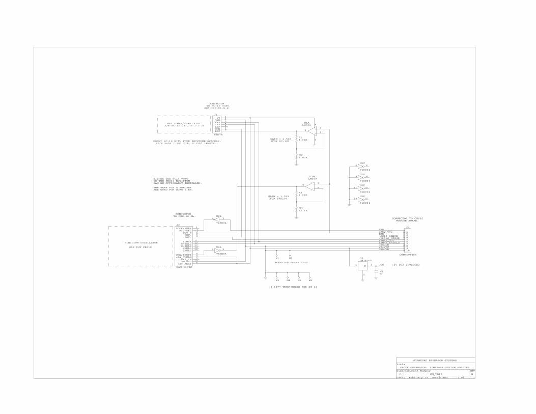
Date: February 15, 2005 Sheet 1 of 1
Size Document Number REV
C CG_TB1B B
Title
CLOCK GENERATOR: TIMEBASE OPTION ADAPTER
STANFORD RESEARCH SYSTEMS
P/N SC-10-24-1-J-J-J-J)SRS 10MHz/+24V OCXO
CONNECTORTO SC-10 OCXO.
SSW-107-01-S-S
+V 1
GND 2
+RF 3
-RF 4
REF 5
GND 6
EFC 7
J1
HED7A
3
2 1
8
4
U1ALM358
5 6U2C
74HC04
GAIN = 2.50X(FOR SC-10)
R22.00K
R13.01K
MOUNT SC-10 WITH FOUR KEYSTONE SPACERS,(P/N 3403 (.25" DIA, 0.125" LENGTH.)
EITHER THE SC10 OCXOOR THE PRS10 RUBIDIUMCAN BE OPTIONALLY INSTALLED.
THE SAME PCB & BRACKET ARE USED FOR OCXO & RB.
GAIN = 1.25X(FOR PRS10)
R33.01K
R412.1K
5
6 7
U1BLM358
13 12U2F
74HC04
11 10U2E
74HC04
9 8U2D
74HC04
RXD
TXD
10MHZ_SHIELD10MHZ_OUT
+24VDC
-PRS10_SENSE-SC10_SENSE
CONNECTOR TO CG635MOTHER BOARD.
FREQ_CTL
GROUND
GROUND
12345678910
J3
CONN10F156
3 4U2B
74HC04
1 2U2A
74HC04
CONNECTORTO PRS-10 Rb.
LOCK/1PPS 1
RXD/EFC 7
POT_W 2
POT+ 8
POT- 3
10MHZ 11
SHIELD 12
+24_HEAT 6GROUND 101PPS_IN 5+24_CLEAN 9TXD/PHOTO 4
SHIELD 13
SHELL 14
SHELL 15
J2
DAM-11W1S
RUBIDIUM OSCILLATOR
SRS P/N PRS10
MOUNTING HOLES:4-40
0.187" THRU HOLES FOR SC-10
M1 M2
M3 M4 M5 M6
1 O 3
2
U3LM78L05
+5V FOR INVERTER
C1C
VCC