From Bubble Chamber to TPC: Where are we going next … Chamb… · From Bubble Chamber to TPC:...
27
From Bubble Chamber to TPC: Where are we going next with detectors? Veljko Radeka [email protected] RHIC & AGS Users Meeting June 22, 2017 1 •Where are we now? •How did we get here? A glimpse at the history … •What challenging developments do we see in the future? V. Radeka, BNL 70
Transcript of From Bubble Chamber to TPC: Where are we going next … Chamb… · From Bubble Chamber to TPC:...

From Bubble Chamber to TPC: Where
are we going next with detectors?
Veljko Radeka [email protected]
RHIC & AGS Users Meeting
June 22, 2017
1
•Where are we now? •How did we get here? A glimpse at the history … •What challenging developments do we see in the future?
V. Radeka, BNL 70

2
“History will be kind to us ... … I intend to write it” ( W.C. ~1945)
Caveat … … about any historical account given by a participant:
Disclaimer : … there is no up to date list of detectors. A new detector is being developed somewhere at this time … in many institutions … Only a few will be mentioned in this talk …. No, I may not mention your valuable work!
V. Radeka, BNL 70

3
ATLAS Diameter 25 m Barrel toroid length 26 m End-cap end-wall chamber span 46 m Overall weight 7000 tons Power ~10 megawatts !!
~1 million detector elements and signal channels + ~100 million silicon det. pixels
LAr calorimeter, fine granularity (~180,000 channels), uniformity, stability, calibration → Highest confidence limits on Higgs
HIC STAR
BNL has played a key role in the concept and construction of Liquid Argon (LAr) Calorimeter and Cathode Strip Chambers (CSC) V. Radeka, BNL 70

Si Vertex Detector based on MAPS – at RHIC STAR
MAPS by IPHC-Strasbourg SVT construction by LBNL and UT Austin, Tx
356 M pixels, 20.7 µm X 20.7 µm, on ~0.16 m2 of Silicon
See: L. Greiner, FEE 2014 4

5
Particle Tracking-Imaging Detectors, 1947 - 1975
Cloud Chamber (Wilson 1911)
Bubble Chamber (Glaser 1952)
Super-saturated, super cooled vapor (temperature just below the boiling point):
- ions act as centers for droplet formation
Super-heated liquid (hydrogen at temperature just above the boiling point):
- gas bubbles form along the particle track
V. Radeka, BNL 70
Particle disoveries → Nobel Prizes

6
Spark Chambers in Muon Neutrino Discovery Lederman, Schwartz, Steinberger,1962, Nobel Prize 1988
10 tons of Al plates
13m of Fe
Muon track
Spark Chambers also in CP Violation Experiment, Fitch and Cronin, 1964, Nobel Prize 1980
V. Radeka, BNL 70
AT BNL AGS:

7
(R)evolution of Tracking Detectors Photographic to Electronic
Cloud chamber
meson
positron
electron
Bubble chamber: charmed baryon decay 1975
STAR TPC Au on Au 2000-
Positron discovery 1932
BNL 1948
V. Radeka, BNL 70

8
Germanium Detector Breakthrough 1963
A.J. Tavendale
Coaxial det.contacts
Ge-crystal ~50-100 cm3
Large Ge detectors 1968
V. Radeka, BNL 70
BNL charge preamp with JFET at ~120K, 1968

9
Germanium vs Sodium Iodide for gamma-ray
spectrometry
Low noise electronics (first cold JFETs) and signal processing (for gamma ray energy resolution of ~0.1%) developed for germanium detectors in ~ 1965-1970. It provided the basis for later use of these techniques in particle physics, and almost all detectors in use presently. 1821.2 keV
V. Radeka, BNL 70

10 Solar Neutrino Detection, Ray Davis, Nobel 2002 Gas proportional counter
used to count 37Ar decays by detecting 2.8 keV Auger
electrons
1948
Nanosecond charge detection to distinguish 37Ar decays from background 10
V. Radeka, BNL 70

Select events in detector technology with long lasting impact …
• Germanium p-i-n detector, Tavendale (1963-4), gamma-ray and x-ray spectroscopy
• Liquid Argon Ionization Calorimetry (1972) → ATLAS • TPC , Nygren (1974), lasting impact through gas and noble liquid TPCs • Planar processing of silicon detectors, Kemmer (1980), basis for future
silicon detectors • Silicon Drift Detector, Gatti and Rehak (1983), p-n CCD, x-ray
spectroscopy, • Back Illuminated Fully Depleted MOS CCD, Holland (1988), astrophysics • Transition Edge Sensors, (1940s→1990s), astrophysics (CMB, BiCEP, x-ray
spectroscopy) • CMOS 0.25µm node (1993), 5nm gate oxide →radiation resistance opens
the door for integration of sensors with electronics at LHC (1990-) • Geiger mode avalanche photo diode, SiPM, (1960s→1990), • Monolithic Active Pixel Sensors (MAPS), IPHC-Strasbourg (~2000) • Gas Electron Multiplier (GEM), Sauli (1997) •
11 V. Radeka, BNL 70

Where is prediction on detectors possible for the next ~ 20 years?
LHC upgrades I and II:
Increasing level 1 trigger rate from LAr calorimetry; new all-silicon tracking
LAr TPCs: scaling up to 10-40 kton range
TPCs for 0ββ-decay, dark matter : scaling up to ton size
Detectors for astrophysics; photon science; PET; neutron scattering, ….
e+-e- collider
SLHC e-ion collider
Integration of “Chambers” and Microelectronics
Silicon: - Strips/pixels
(bump/directly bonded) - MAPS - SiPMs
TPCs - Gas and noble
liquid, charge and light
12
“Microelectronics” Beyond CMOS??
V. Radeka, BNL 70

Si “Pixel” Detectors
sensor ASIC(s)
Sensor pixels bump-bonded to ASIC pixels
pixel
pixel channel
Sensor pixels fusion-bonded to (2D or 3D) ASIC pixels
3D pixel channel
13
Monolithic Active Pixel Sensors (MAPS): sensor and transistors in “standard” CMOS technology – new developments for ALICE and sPHENIX

Advances in MAPS • From diffusion to drift for charge collection→ ~100ns to <10ns • Increased epitaxial layer resistivity from ~20ohm cm to 1kohm cm • From rolling shutter to faster readout → ~170mW/cm2 to 5mW/cm2
From: G. Contin, LBL
MAPS

Silicon Photo Multiplier (SiPM) • ”Geiger-mode”: avalanche spends itself (“quenches”) by reducing the cell voltage • Principal advantage: single electron produces ~106 electrons • Principal disadvantage: single electron produces ~106 electrons
Secondary electrons α avalanche size
50 µm micro-pixel ~40,000/cm2
Future: Diverse applications, innovation in device design and integration with readout electronics
Large arrays
C. Piemonte
Single p.e. resolution

Time Projection Chambers (TPCs) with
Gas or Noble Liquids “Electronic Bubble Chambers”
16 V. Radeka, BNL 70

Fine Granularity Gas TPCs:
HV Cathode Plane Double GEM planes
Interpolating anode pad plane with front end ASICs (7296 channels) in the LEGS TPC; 10 watts total on TPC.
Digital readout board
Field cage
1. GEM 2. Interpolating anode configuration - chevron 3. Anode-pad–ASIC board topology 4. S/N, minimize capacitance, gas gain and
positive ion space charge
17
Bo Yu et al. (BNL, 2002)
V. Radeka, BNL 70
time
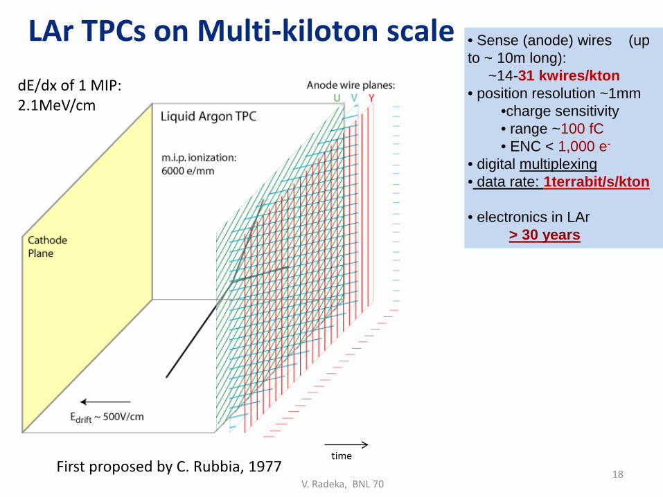
• Sense (anode) wires (up to ~ 10m long): ~14-31 kwires/kton • position resolution ~1mm
•charge sensitivity • range ~100 fC • ENC < 1,000 e-
• digital multiplexing • data rate: 1terrabit/s/kton • electronics in LAr
> 30 years
dE/dx of 1 MIP: 2.1MeV/cm
LAr TPCs on Multi-kiloton scale
First proposed by C. Rubbia, 1977 18 V. Radeka, BNL 70

MicroBooNE LAr TPC: 62 m3 fiducial vol. (87 tons)
19 V. Radeka, BNL 70
FE electronics in LAr
2.5x2.5x10m3

LXe TPC with Charge and Light sensing (e.g., 0νββ decay experiment) ~2 ton scale (nEXO)
20
Challenge: SiPMs to cover large areas (~5 sq. meters) in noble liquid detectors → large number of SiPMs to read out (>104, dark count rate ~ 108/s)
Electronics in LXe (~160K) for both charge and light
V. Radeka, BNL 70

CMOS and Device Future
21
End of Moore’s Scaling? Beyond CMOS? What after CMOS?
V. Radeka, BNL 70
• Number of transistors/die → functionality α 1/L
• speed α 1/L • cost/transistor α 1/L • power dissipation/area
L/tox~50 W/L~0.1
- 106 tox

1960 1970 1980 1990 2000 2010 2020 2030 2040100p
1n
10n
100n
1µ
10µ
Through-Si Vias (TSV)
3D + 3D3D
2.5D
1MHz
32nm 1.1
V
Si 0.54nm
> 3GHzXbox One 28nm
6-core I7 45nm
20nm 0.9
V45n
m 1.1V
Intel 80286
L 10 µ
m 12Vfirst MOSFET
first IC
Intel 80486
10-core XEON 32nm
Intel 4004
16nm Fin
FET 0
.7V
28nm 1.0
V65n
m 1.2V
90nm 1.2
V
130nm
1.5V
180nm
1.8V
250nm
2.5V
500nm
3.3V
1.2µm
5V
Tran
sist
or c
hann
el le
ngth
L
Year
100
1k
10k
100k
1M
10M
100M
1G
10G
100G
Num
ber o
f tra
nsis
tors
/ di
e
Devices on sensors
CMOS maturing …
5-7nm?
V. Radeka, BNL 70 From: G. De Geronimo
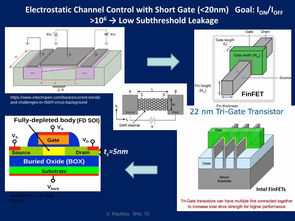
Electrostatic Channel Control with Short Gate (<20nm) Goal: ION/IOFF >106 → Low Subthreshold Leakage
TFIN
Buried Oxide (BOX)Substrate
Fully-depleted body
Gate
VG
VS VD
DrainSource
Vback
Buried Oxide (BOX)Substrate
Fully-depleted body
Gate
VG
VS VD
DrainSource
Vback
ts≈5nm
Adapted from: S.K. Gupta, FEE2014
23 V. Radeka, BNL 70
https://www.intechopen.com/books/current-trends-and-challenges-in-rfid/rf-cmos-background
(FD SOI)
FinFET
Intel FinFETs
Graphene nanotube

Alternate Device Concepts
24
Physical (computational) variables: charge, current, voltage, electric dipole,magnetic dipole, orbital state Devices considered by NRI: - tunelling FET - graphene nanoribbon FET - bilayer pseudospin FET - SpinFET - spin transfer torque/domain wall - spin majority gate - spin transfer torque triad - spin torque oscillator logic - all spin logic device - spin wave device - nanomagnet logic - III-V tunnel FETs
Upon analysis: Spintronic devices have longer switching delays and higher switching energies, due to inherent time of magnetization propagation …
Entirely new concepts (… and dreams): - Selfassembly of nanoscale devices (single-port devices possibly, no three-terminal devices yet) - Stochastic computing: no longer deterministic logic with defective devices acceptable,
V. Radeka, BNL 70

“Beyond CMOS?” Why is it so difficult to find a “better”(smaller, faster, lower power) device?
Any “Beyond CMOS” device should have many of the same characteristics as CMOS devices : - power gain >1 - ideal signal restoration and fanout - high ON/OFF current ratio ~105-7
(low static power dissipation) - compatibility with Si CMOS devices for mixed functions
From: F. Schwierz
CMOS NAND Gate:
25
More likely, a gradual evolution: New, or special functions (e.g., memories) may become possible in the nanoscale devices by new physics and such devices may be
merged into CMOS circuits to enhance overall performance. Impedance matching may be necessary from the quantum resistance values (kohm) down to the 50-100ohm
range. The overall logic operations and communications will still be based on CMOS.
The consensus : No new device is on the horizon with a potential to completely replace CMOS
V. Radeka, BNL 70

What to expect for electronics integrated into particle detectors?
• It will remain CMOS based (albeit with new materials) well into the mid-century. • The channel length will level off somewhere below 10nm in semiconductor industry with expansion into 3D and new channel and gate dielectric materials. • Science community has followed the minimum channel length with a delay in actual use of ~ 10 years. This may increase. • The choice of technology node (e.g., 10nm vs 65nm) for high resolution detectors may depend on device parameter variations which increase with 1/L. • Minimum noise for capacitive sensors (science applications) will require channel lengths longer than minimum feature size (for 1/f noise in particular). • The time and effort for design of more complex ASICs has been increasing steeply with scaling: increasing functionality+growing design rules+more complex and costly design tools, more costly prototyping, extensive testing effort, unique design features for particle detectors.
•
V. Radeka, BNL 70

Concluding remarks:
The future of particle detectors to be developed with advancing electronics technology is exciting.
To take full advantage (or, just to keep up) will be a challenge for research institutions and funding
agencies …
… with all this you can work happily into 2050s !
Thank you!
V. Radeka, BNL 70 27