6A Power-Efficient 33 GHz 2 1 Static Frequency Divider in 0.12-Pm
This is a repository copy of Frequency-selectable dual-band wilkinson divider/combiner.
White Rose Research Online URL for this paper:http://eprints.whiterose.ac.uk/82382/
Version: Accepted Version
Article:
Chongcheawchamnan, M, Julrat, S, Shafique, MF et al. (1 more author) (2013) Frequency-selectable dual-band wilkinson divider/combiner. IET Microwaves, Antennas and Propagation, 7 (10). 836 - 842. ISSN 1751-8725
https://doi.org/10.1049/iet-map.2013.0113
[email protected]://eprints.whiterose.ac.uk/
Reuse
Unless indicated otherwise, fulltext items are protected by copyright with all rights reserved. The copyright exception in section 29 of the Copyright, Designs and Patents Act 1988 allows the making of a single copy solely for the purpose of non-commercial research or private study within the limits of fair dealing. The publisher or other rights-holder may allow further reproduction and re-use of this version - refer to the White Rose Research Online record for this item. Where records identify the publisher as the copyright holder, users can verify any specific terms of use on the publisher’s website.
Takedown
If you consider content in White Rose Research Online to be in breach of UK law, please notify us by emailing [email protected] including the URL of the record and the reason for the withdrawal request.
Frequency-Selectable Dual-Band Wilkinson Divider/Combiner
M. Chongcheawchamnan and S. Julrat
Computer Engineering Department
Prince of Songkla University
Songkhla, Thailand
M. Farhan Shafique
Center for Advanced Study in Telecommunication
COMSATS Institute of Information Technology
Islamabad, Pakistan
I. D. Robertson
Institute of Microwaves and Photonics
University of Leeds, UK
*Corresponding author: Mitchai Chongcheawchamnan ([email protected]).
Frequency-Selectable Dual-Band Wilkinson Divider/Combiner
A technique for realizing a compact frequency-selectable dual-band Wilkinson
divider/combiner is presented in this paper. To provide a frequency-selection function, the band-
pass transmission-line transformer in a dual-band device is replaced with a tuneable band-reject
transmission-line transformer. To realize this tuneable device, a variable capacitively-loaded
spur-line filter is proposed for its compact size. The theory based on an ideal transmission-line
circuit is developed to provide a design procedure. The proposed circuits are demonstrated with
simulated and measured results of a Wilkinson divider/combiner fabricated on FR4 substrate.
Keywords: Wilkinson power divider; dual-band power divider; passive circuits; microwave
integrated circuits.
1. INTRODUCTION
The Wilkinson power divider/combiner is among the most commonly used passive
components in microwave and millimetre-wave circuits and systems [1]-[2]. The
conventional design for this component uses quarter-wave lines that operate at a single
frequency. With ever increasing demand for multi-band and multifunction
mobile/handheld devices, several multiband design techniques have been proposed [3]-
[9]. Most previous research works proposed new circuit topologies that are able to
operate in several bands simultaneously while their circuit sizes are kept small.
However, there is a need to design a multi-band communication system operating in
non-concurrent mode, for example in a phased array receiver, a low-noise balanced
amplifier, or a satellite transceiver, to name a few.
Phased-array receiver systems have been long applied in satellite and military
communications due to the excellent sensitivity performance [10-13]. There is a lot of
interest from researchers in applying phased arrays to commercial wireless
communication application such as in wireless local area networks and cellular mobile
systems. In radar, a phased-array can track multiple targets. In these applications, a
multi-band or a wideband phased-array receiver is needed. A frequency-selectable
multi-band power splitter/combiner is a valuable component for the frontend of such
systems. The Wilkinson power divider/combiner is a good design choice due to its
simple design and implementation. Therefore, in this paper we demonstrate a simple
design for a frequency-selectable dual-band power divider/combiner. The proposed
concept can be extended to design a frequency-selectable multi-band power
divider/combiner as well.
One way to realise a frequency selectable dual-band Wilkinson divider/combiner
is simply to connect two circuits in parallel which operate in the two desired bands. The
operating band can be selected by using electronic, mechanical, or optical switching
techniques. Unfortunately this simple approach leads to a bulky design. On the other
hand, most of the previously proposed dual-band Wilkinson circuits are not appropriate
because they lack any frequency selection mechanism.
In this paper, we present a simple concept to design a frequency-selectable dual-
band Wilkinson divider/combiner. Starting with a dual-band circuit, a frequency-
selectable function is achieved by embedding a band-reject transmission-line
transformer (TLT) which has a tuning mechanism. Such a TLT can suppress an
unwanted signal in the reject band while allowing the wanted signal through in another
band. Recently, a capacitively-loaded spur-line section was proposed for a tuneable
band-reject filter [14]. This circuit is compact and can be applied as a tuneable band-
reject TLT. To illustrate this, we apply the frequency-selectable TLT concept to two
previously proposed dual-band circuits [7]-[8]. This results in a frequency-selectable
dual-band Wilkinson divider/combiner. This design is chosen due to its compact size
and simple implementation. It should be noted that the proposed concept can also be
applied to other circuits.
The proposed concept, as well as the variable capacitively-loaded spur-line filter
will be described in Section 2. The design and implementation of the proposed
Wilkinson divider/combiner are presented in Section 3, while the measured results are
given in Section 4. Finally, the paper will be concluded in Section 5.
2. FREQUENCY-SELECTABLE DUAL-BAND TRANSMISSION-LINE
TRANSFORMER
A single-band Wilkinson divider/combiner can be realized with a TLT. The main
concept proposed here to realize a dual-band component for these two circuits is to
replace a standard TLT with a dual-band TLT [3]-[4]. This is also applicable for several
multi-band designs [5]. In a similar way, designing a frequency-selectable dual-band
Wilkinson divider/combiner can be achieved by adding a frequency selectable
mechanism to a dual-band TLT in those conventional dual-band designs.
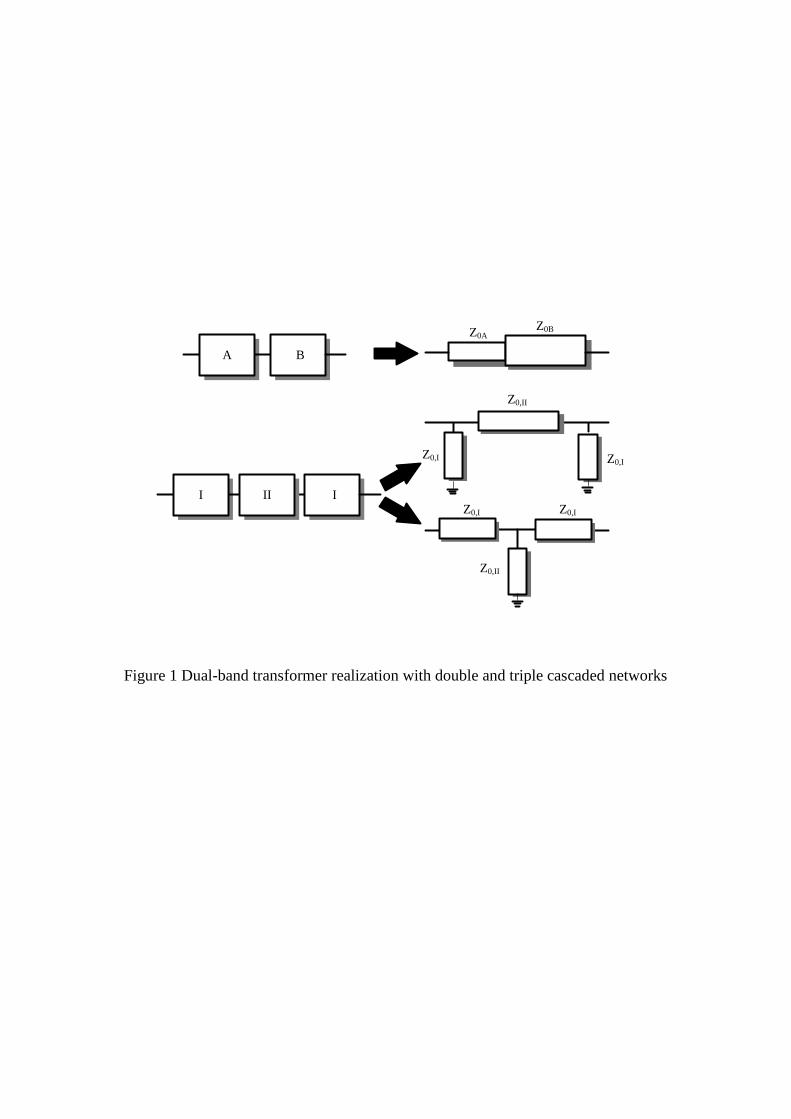
Several network topologies for a dual-band transformer have been proposed.
The basic component is a transmission line. A dual-band TLT may be simply designed
by cascading several transmission line circuits as shown in Figure 1. A two-section TLT
is one of the dual-band transformer design examples which can be achieved by
cascading two transmission line sections. Cascading three sections can be done in the
form of either a T-or ぢ-network. For such a case, a one-port network topology realized
with either a short or open circuit transmission line is needed. It should be noted that a
dual-band transformer formed with a symmetrical T- or ぢ-network is preferable for
realizing a symmetrical microwave circuit. As it is more generally applicable than the
two-section TLT, we therefore develop a frequency-selectable dual-band transformer
based on a T- or ぢ-network topology.
By adding a mechanism to control the passband in the T- or ぢ-network shown in
Figure 1, a tuneable band reject function is given to the transmission line in the three-
section network. This may be achieved by either cascading a tuneable band reject filter
(BRF) to the network or replacing the transmission line with a tuneable BRF. Either
way, the size of the new circuit should be negligibly increased as compared with the
original size. The approach to cascade a BRF with the network shown in Figure 1 is not
of interest since it unavoidably increases the circuit size. We therefore choose the
second approach and apply it to the three-section network.
A variable capacitively-loaded spur-line filter shown in Figure 2a) is selected as
a tuneable BRF in this paper due to its compact size [14]. It is composed of a spur-line
filter with a variable capacitor connected across the ends of the coupled lines. This
tuneable spur-line filter is characterized by its characteristic impedance and electrical
length. Here, we will only focus on a spur line design based on symmetrical coupled
lines. We assume that the coupled lines are lossless, hence the ideal transmission-line
model can be applied when the tuneable spur line is analyzed. The even- and odd-mode
characteristic admittances of the coupled lines in Figure 2(a) are denoted by Y0e and Y0o.
The electrical length defined at the first operating frequency f1 is 肯. The coupling
coefficient of the coupled lines determines the bandwidth for each stopband and also the
response of the circuit. Tight coupling is needed if a narrow stopband is desired.
However, the fabrication limitations have to be carefully considered in practice. The
variable capacitor Ci (i = 1,2) provides a mechanism to tune a stopband frequency at

血沈.With a system admittance Y0 defined at spur-line ports a and b, the scattering
parameters at frequency f of this tuneable spur line filter are [14]:
嫌銚銚岫血┸ 系沈岻 噺 なッ岫血┸ 系沈岻 釆桁待態 犯岫桁待勅 髪 桁待墜岻 cot 磐肯 血血怠卑 伐 ね講血系沈般 髪 ね桁待勅態 犯ね講血系沈 伐 桁待墜 cot 磐肯 血血怠卑般 伐 倹に桁待桁待勅態 挽 (1a),
嫌銚長岫血┸ 系沈岻 噺 嫌長銚岫血┸ 系沈岻 噺 倹ね桁待桁待勅 csc 岾肯 捗捗迭峇 峙ね講血系沈 伐 桁待墜 cot 岾肯 捗捗迭峇峩ッ岫血┸ 系沈岻
(1b),
嫌長長岫血┸ 系沈岻 噺 なッ岫血┸ 系沈岻 釆桁待態 犯岫桁待勅 髪 桁待墜岻 cot 磐肯 血血怠卑 伐 ね講血系沈般 髪 ね桁待勅態 犯ね講血系沈 伐 桁待墜 cot 磐肯 血血怠卑般 髪 倹に桁待桁待勅態 挽 (1c),
where
ッ岫血┸ 系沈岻 噺 桁待態 犯岫桁待勅 髪 桁待墜岻 cot 磐肯 血血怠卑 伐 ね講血系沈般 髪 ね桁待勅態 犯桁待墜 cot 磐肯 血血怠卑 伐 ね講血系沈般髪 倹に桁待桁待勅 崕桁待勅 髪 ぱ講血系沈 cot 磐肯 血血怠卑 伐 に桁待墜 釆cot 磐肯 血血怠卑挽態崗
(1d).
By inspecting only (1b), one can find that the frequency stopband at fi will be obtained
if Ci is tuned to:
系沈 噺 超轍任 達誰担岾肉日肉迭提峇替訂捗日 (2).
Substituting (2) into (1a)-(1d) and simplifying further, the frequency responses of the
tuneable spur line at fi are:
嫌銚銚岫血沈岻 噺 超轍 達誰担岾提肉日肉迭峇貸珍態超轍賑超轍 達誰担岾提肉日肉迭峇袋珍態超轍賑 (3a),
嫌銚長岫血沈岻 噺 嫌長銚岫血沈岻 噺 ど (3b),
嫌長長岫血沈岻 噺 な (3c).
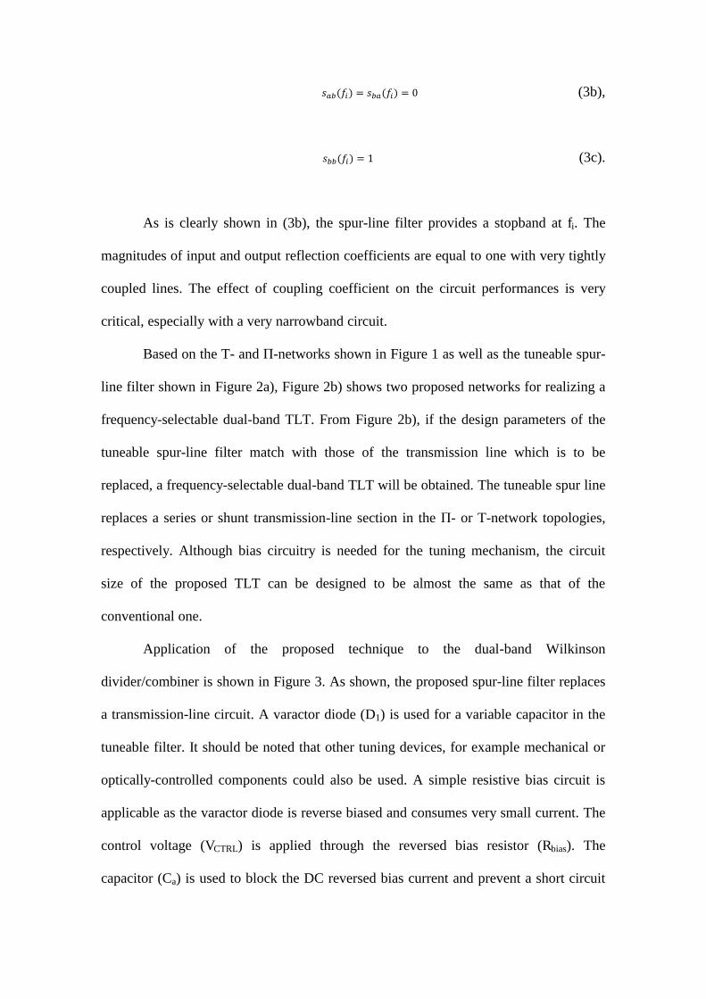
As is clearly shown in (3b), the spur-line filter provides a stopband at fi. The
magnitudes of input and output reflection coefficients are equal to one with very tightly
coupled lines. The effect of coupling coefficient on the circuit performances is very
critical, especially with a very narrowband circuit.
Based on the T- and ぢ-networks shown in Figure 1 as well as the tuneable spur-
line filter shown in Figure 2a), Figure 2b) shows two proposed networks for realizing a
frequency-selectable dual-band TLT. From Figure 2b), if the design parameters of the
tuneable spur-line filter match with those of the transmission line which is to be
replaced, a frequency-selectable dual-band TLT will be obtained. The tuneable spur line
replaces a series or shunt transmission-line section in the ぢ- or T-network topologies,
respectively. Although bias circuitry is needed for the tuning mechanism, the circuit
size of the proposed TLT can be designed to be almost the same as that of the
conventional one.
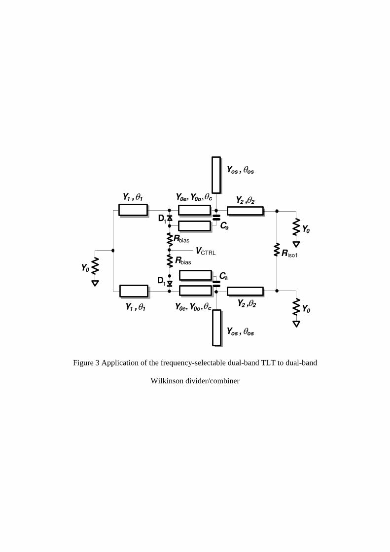
Application of the proposed technique to the dual-band Wilkinson
divider/combiner is shown in Figure 3. As shown, the proposed spur-line filter replaces
a transmission-line circuit. A varactor diode (D1) is used for a variable capacitor in the
tuneable filter. It should be noted that other tuning devices, for example mechanical or
optically-controlled components could also be used. A simple resistive bias circuit is
applicable as the varactor diode is reverse biased and consumes very small current. The
control voltage (VCTRL) is applied through the reversed bias resistor (Rbias). The
capacitor (Ca) is used to block the DC reversed bias current and prevent a short circuit
occurring at the coupled lines. Since the electrical length of the tuneable spur line is
equal to that of the replaced transmission-line section, the overall size of the proposed
frequency-selectable dual-band Wilkinson divider/combiner is similar to the size of the
original designs which were reported in [7] and [8].
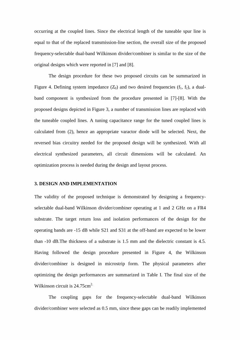
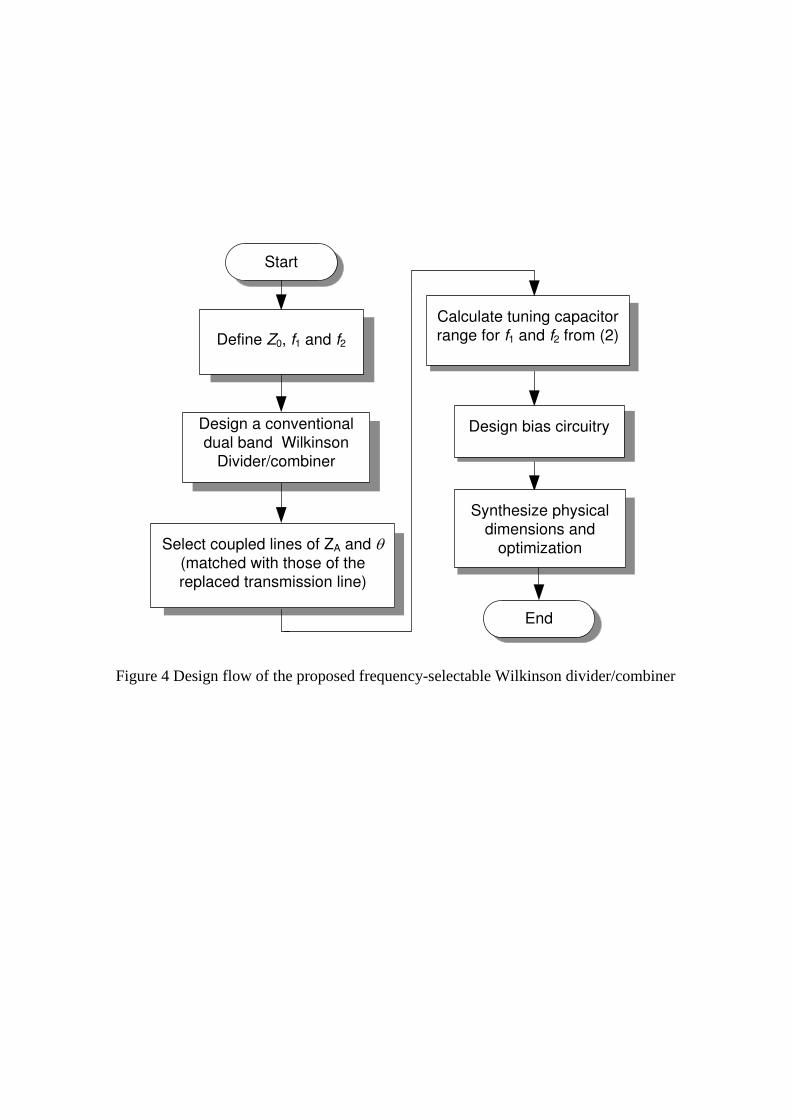
The design procedure for these two proposed circuits can be summarized in
Figure 4. Defining system impedance (Z0) and two desired frequencies (f1, f2), a dual-
band component is synthesized from the procedure presented in [7]-[8]. With the
proposed designs depicted in Figure 3, a number of transmission lines are replaced with
the tuneable coupled lines. A tuning capacitance range for the tuned coupled lines is
calculated from (2), hence an appropriate varactor diode will be selected. Next, the
reversed bias circuitry needed for the proposed design will be synthesized. With all
electrical synthesized parameters, all circuit dimensions will be calculated. An
optimization process is needed during the design and layout process.
3. DESIGN AND IMPLEMENTATION
The validity of the proposed technique is demonstrated by designing a frequency-
selectable dual-band Wilkinson divider/combiner operating at 1 and 2 GHz on a FR4
substrate. The target return loss and isolation performances of the design for the
operating bands are -15 dB while S21 and S31 at the off-band are expected to be lower
than -10 dB.The thickness of a substrate is 1.5 mm and the dielectric constant is 4.5.
Having followed the design procedure presented in Figure 4, the Wilkinson
divider/combiner is designed in microstrip form. The physical parameters after
optimizing the design performances are summarized in Table I. The final size of the
Wilkinson circuit is 24.75cm2.
The coupling gaps for the frequency-selectable dual-band Wilkinson
divider/combiner were selected as 0.5 mm, since these gaps can be readily implemented
with the in-house fabrication process. Variable capacitors in the circuits are
implemented with a BB857 varactor diode in the surface mount device (SMD) package.
The capacitor range of this diode is 0.5-6.6 pF when a reverse bias range of 0 to 30 V is
applied. A resistor of 56 kっ is selected for biasing this diode. The isolation resistor,
RISO1, in the Wilkinson divider/combiner is selected as 100っ. A surface mount
technology (SMT) capacitor of 40 pF was selected for the DC blocking capacitor.
The circuit was laid out using the Agilent Technologies MomentumTM software.
A symmetrical layout was required to preserve the symmetrical property of the circuit
response. The diode model presented in [15]-[16] was included in the simulation. The
values of parasitic components for the SMD package are illustrated in Figure 5.The
open transmission lines in the Wilkinson divider/combiner were converted to curved
linesto minimize the circuit size, t. The ends of each transmission line pair at port 2 and
3 are tapered such that the gap between -port 2 and 3 fit with the size of SMT isolation
resistor (model 0405). This leads to good matching and isolation at port 2 and 3 for the
Wilkinson design at both frequencies.
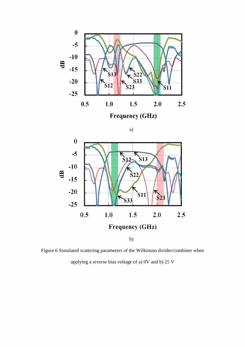
The simulated scattering parameters of the design using MomentumTM are
shown in Figure 6. Figure 6 a) and b) demonstrate the performances of the Wilkinson
divider/combiner. The results show good matching at all ports for both bands. The
performance of the Wilkinson circuit is not very sensitive to coupling coefficient since
the operating band of the Wilkinson circuit is generally broad.
4. MEASURED RESULT AND DISCUSSIONS
Photograph of the Wilkinson circuit is shown in Figure 7. The measurements were
performed with a vector network analyzer (HP8510C). A short-open-load-thru (SOLT)
calibration from 0.05-6 GHz was performed before making measurement. SMA
connectors were used to interface the circuits with the network analyzer via coaxial
cables. The bias voltage was applied from a power supply (GPR-3510HD). By
terminating with a 50 っ standard SMA load, each two-port scattering parameter set was
measured. All data sets were collected and post processed using the Agilent
Technologies Advanced Design System TM.
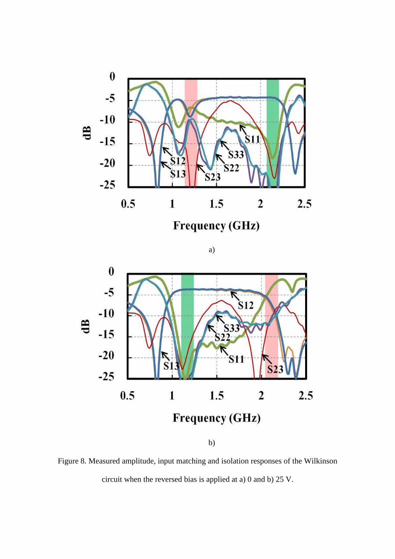
Figure 8 a) and b) show the measured S11, S21, S31 and S23 of the Wilkinson
circuit when the reverse bias is applied at 0 and 25 V, respectively. Excellent amplitude
balance between port P2 and P3 is obtained for the two reversed bias conditions. When
0 V is applied, the operating frequency shifts from the designed 2 GHz to 2.2 GHz as
shown in Figure 8a). On the other hand, the operating frequency shifts from the
designed1 GHz to 1.2 GHz when 25 V is applied as shown in Figure 8b). This
frequency shift is expected from the limitation of our fabrication tolerance and the
parasitics of SMD components. From Table 2, the matching and isolation performances
are better than -18 dB in both operating bands.S21 and S31 are around -3.8 dB in both
operating bands. We believe that the increased loss mainly results from the parasitic
resitance from the diode and the DC blocking capacitor used in our design. The
straightforward method to obtain low insertion loss in these circuits is to choose other
low loss tuning techniques, for example an optical or ferromagnetic tuning technique.
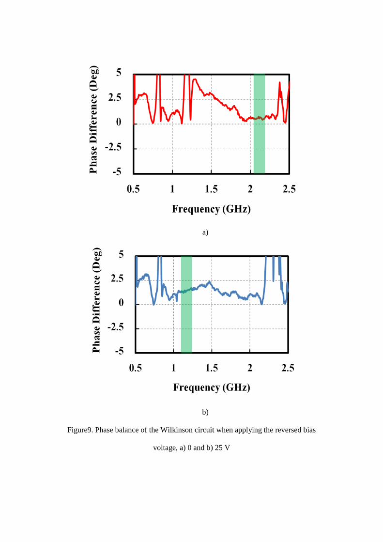
Figure 9 a) and b) shows the phase balance performance of the Wilkinson circuit
for two reversed bias voltages, 0 and 25 V, respectively. Excellent phase balance occurs
in both bands for each reversed bias condition. This is comes from the symmetrical
layout in our design.
5. CONCLUSION
A frequency-selectable Wilkinson divider based on the proposed frequency-selectable
dual-band transmission-line transformer has been demonstrated. The mechanism for
tuning the frequency of the transmission-line transformer is a capacitively-loaded spur-
line filter using a varactor diode. It has been shown that this frequency-selectable
Wilkinson divider provides a compact design and is hence suited for low-cost solutions.
Compared with the prototype dual-band structure, no extra area is needed for the
proposed technique. We also present the design procedure for the proposed circuits.
Experimental results show the feasibility of the technique. Parasitic resistance from the
varactor diode and DC blocking capacitor should be carefully taken into account during
the design. To obtain better performance for the proposed design, other low loss tuning
techniques are recommended. We believe that the proposed components suits for a
number of applications including phased-array receivers.
ACKNOWLEDGEMENT
This research is financially supported by Telecommunications Research & Industrial
Development Institute (TRIDI) under grant number TARG 2553/004. Ian D. Robertson
would like to acknowledge the support of EPSRC (3D Microwave & Millimetre-Wave
System-on-Substrate using Sacrificial Layers for Printed RF MEMS Components).
REFERENCES
1. Chang, K., Encyclopedia of RF and Microwave Engineering, Wiley-Interscience,
2005.
2. Robertson, I. D. and S. Lucyszyn, RFIC and MMICs design, IEE, 2002.
3. Srisathit, S., S. Virunphun, K. Bandudej, M. Chongcheawchamnan, and A.
Worapishet, “A dual-band 3-dB three-port power divider based on a two-section
transmission line transformer,” in IEEE MTT-S Int. Microwave Symp. Dig., Vol. 1,
35–38, 2003.
4. Srisathit, S., M. Chongcheawchamnan, A. Worapishet, “Design and realisation of a
dual-band 3-dB power divider based on a two-section transmission-line topology,”
Electronics Letters, Vol. 29, No. 9,723-724, 2003.
5. Chongcheawchamnan, M., S. Patisang, M. Krairiksh, and I. Robertson, “Tri-band
Wilkinson power divider using a three-section transmission-tine transformer,”
IEEE Microw. Wireless Compon. Lett., Vol. 16, No.8, 452–454, 2006.
6. Qaroot, A. M. and N. I. Dib, "General design of n-way multi-frequency unequal
split Wilkinson power divider using transmission line transformers," Progress In
Electromagnetics Research C, Vol. 14, 115-129, 2010.
7. Wu, L., Z. Sun, H. Yilmaz, and M. Berroth, “A dual-frequency Wilkinson power
divider”, IEEE Trans. on Microwwave Theory and Techniques, Vol. 54, No.1, 278-
284, 2006.
8. Cheng, K.-K. M., and F.-L.Wong, “A new Wilkinson power divider design for
dual-band applications,” IEEE Microw. WirelessCompon.Lett., Vol. 17, No.9, 664–
666, 2007.
9. Power divider and power combiner using dual-band composite right/left handed
transmission line, United Stated Patent, US 2010/0026416 A1.
10. Jeon S. et al., “A scalable 6-to-18 GHz concurrent dual-band quad-beam phased-
array receiver in CMOS”, IEEE Journal of Solid-State Circuits, Vol. 43, No.12,
2660-2673, 2008.
11. Katajamaki, T. Radionet, “A compact dual-band phased array antenna for outdoor
WLAN”, IEEE Vehicular Technology Conference, Vol.1, 59-63, 2004.
12. Choi, H. J. and T. Itoh, “Dual-band composite right/left-handed (CRLH) phased-
array antenna,” IEEE Antenna and Wireless Propagation Letters, Vol. 11, 732-735,
2012.
13. Kim, J., J. Jeong and S. Jeon, “Improvement of noise performance in phased-array
receivers,” ETRI Journal, Vol. 33, No.2, 176-183, 2011.
14. Chongcheawchamnan, M., M. F, Shafique and I. D. Robertson, “Miniaturization
and electronic tuning techniques for microstrip spuline filters,” IET Microws.,
Antennas, and Prop.,Vol. 5, No.1, 1-9, 2011.
15. Infineon Technologies AG: BB857 Data Sheet and BB857 Simulation Data,
http://www.infineon.com, January 2009.
16. Vokac, M., “Phase shifter based on varactor-loaded transmission line”, Master
Thesis, Department of Electromagnetic Field, Faculty of Electrical Engineering,
Czech technical university, 2009.

List of Table
Table 1. Dimensions (in mm) of the Wilkinson divider/combiner implementing on FR4
Table 2. Simulated and measured S-parameter of the proposed design
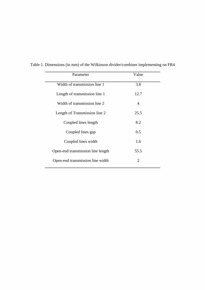
Table 1. Dimensions (in mm) of the Wilkinson divider/combiner implementing on FR4
Parameter Value
Width of transmission line 1 3.8
Length of transmission line 1 12.7
Width of transmission line 2
Length of Transmission line 2
Coupled lines length
4
25.5
8.2
Coupled lines gap 0.5
Coupled lines width 1.6
Open-end transmission line length 55.5
Open-end transmission line width 2
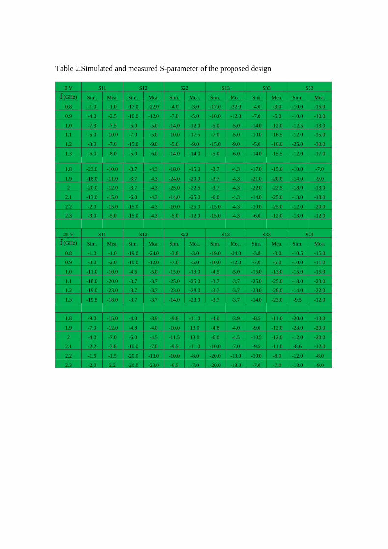
Table 2.Simulated and measured S-parameter of the proposed design
0 V S11 S12 S22 S13 S33 S23
f (GHz) Sim. Mea. Sim. Mea. Sim. Mea. Sim. Mea. Sim Mea. Sim. Mea.
0.8 -1.0 -1.0 -17.0 -22.0 -4.0 -3.0 -17.0 -22.0 -4.0 -3.0 -10.0 -15.0
0.9 -4.0 -2.5 -10.0 -12.0 -7.0 -5.0 -10.0 -12.0 -7.0 -5.0 -10.0 -10.0
1.0 -7.3 -7.5 -5.0 -5.0 -14.0 -12.0 -5.0 -5.0 -14.0 -12.0 -12.5 -13.0
1.1 -5.0 -10.0 -7.0 -5.0 -10.0 -17.5 -7.0 -5.0 -10.0 -16.5 -12.0 -15.0
1.2 -3.0 -7.0 -15.0 -9.0 -5.0 -9.0 -15.0 -9.0 -5.0 -10.0 -25.0 -30.0
1.3 -6.0 -8.0 -5.0 -6.0 -14.0 -14.0 -5.0 -6.0 -14.0 -15.5 -12.0 -17.0
1.8 -23.0 -10.0 -3.7 -4.3 -18.0 -15.0 -3.7 -4.3 -17.0 -15.0 -10.0 -7.0
1.9 -18.0 -11.0 -3.7 -4.3 -24.0 -20.0 -3.7 -4.3 -21.0 -20.0 -14.0 -9.0
2 -20.0 -12.0 -3.7 -4.3 -25.0 -22.5 -3.7 -4.3 -22.0 -22.5 -18.0 -13.0
2.1 -13.0 -15.0 -6.0 -4.3 -14.0 -25.0 -6.0 -4.3 -14.0 -25.0 -13.0 -18.0
2.2 -2.0 -15.0 -15.0 -4.3 -10.0 -25.0 -15.0 -4.3 -10.0 -25.0 -12.0 -20.0
2.3 -3.0 -5.0 -15.0 -4.3 -5.0 -12.0 -15.0 -4.3 -6.0 -12.0 -13.0 -12.0
25 V S11 S12 S22 S13 S33 S23
f (GHz) Sim. Mea. Sim. Mea. Sim. Mea. Sim. Mea. Sim. Mea. Sim. Mea.
0.8 -1.0 -1.0 -19.0 -24.0 -3.8 -3.0 -19.0 -24.0 -3.8 -3.0 -10.5 -15.0
0.9 -3.0 -2.0 -10.0 -12.0 -7.0 -5.0 -10.0 -12.0 -7.0 -5.0 -10.0 -11.0
1.0 -11.0 -10.0 -4.5 -5.0 -15.0 -13.0 -4.5 -5.0 -15.0 -13.0 -15.0 -15.0
1.1 -18.0 -20.0 -3.7 -3.7 -25.0 -25.0 -3.7 -3.7 -25.0 -25.0 -18.0 -23.0
1.2 -19.0 -23.0 -3.7 -3.7 -23.0 -28.0 -3.7 -3.7 -23.0 -28.0 -14.0 -22.0
1.3 -19.5 -18.0 -3.7 -3.7 -14.0 -23.0 -3.7 -3.7 -14.0 -23.0 -9.5 -12.0
1.8 -9.0 -15.0 -4.0 -3.9 -9.8 -11.0 -4.0 -3.9 -8.5 -11.0 -20.0 -13.0
1.9 -7.0 -12.0 -4.8 -4.0 -10.0 13.0 -4.8 -4.0 -9.0 -12.0 -23.0 -20.0
2 -4.0 -7.0 -6.0 -4.5 -11.5 13.0 -6.0 -4.5 -10.5 -12.0 -12.0 -20.0
2.1 -2.2 -3.8 -10.0 -7.0 -9.5 -11.0 -10.0 -7.0 -9.5 -11.0 -8.6 -12.0
2.2 -1.5 -1.5 -20.0 -13.0 -10.0 -8.0 -20.0 -13.0 -10.0 -8.0 -12.0 -8.0
2.3 -2.0 2.2 -20.0 -23.0 -6.5 -7.0 -20.0 -18.0 -7.0 -7.0 -18.0 -9.0

List of Figures
Figure 1. Dual-band transformer realization with double and triple cascaded networks
Figure 2. a) Variable capacitively-loaded spur line; b) its application to the dual-band
TLT
Figure 3.Application of the frequency-selectable dual-band TLT to dual-band
Wilkinson divider/combiner
Figure 4. Design flow of the proposed frequency-selectable Wilkinson divider/combiner
Figure 5. Parasitic model of a varactor diode BB857
Figure6. Simulated scattering parameters of the Wilkinson divider/combiner when
applying a reversed bias voltage of a) 0V and b) 25 V
Figure7. Photograph of the frequency-selectable dual-band Wilkinson divider/combiner
Figure8. Measured amplitude, input matching and isolation responses of the Wilkinson
circuit when the reversed bias is applied at a) 0 and b) 25 V
Figure9. Phase balance of the Wilkinson circuit when applying the reversed bias
voltage, a) 0 and b)25 V
A B
I III
Z0AZ0B
Z0,I Z0,I
Z0,II
Z0,II
Z0,I Z0,I
Figure 1 Dual-band transformer realization with double and triple cascaded networks
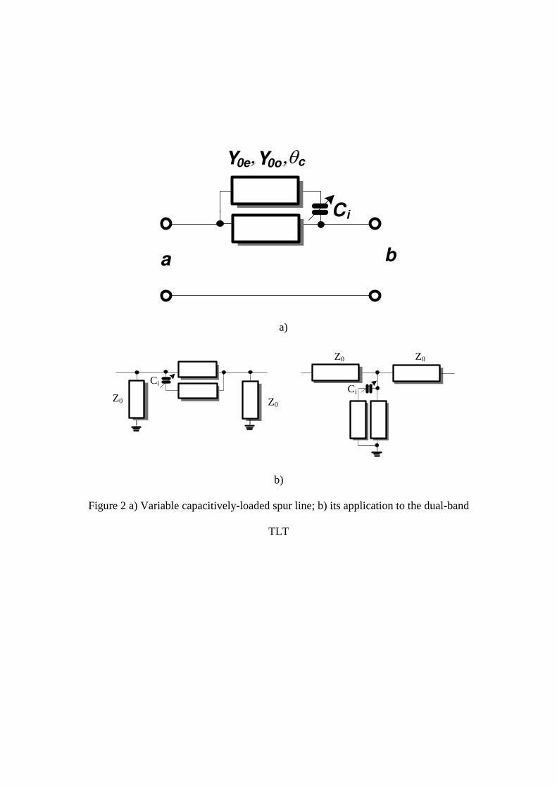
,qcY0e Y0o,
Ci
ba
a)
Z0 Z0
Z0 Z0
CiCi
b)
Figure 2 a) Variable capacitively-loaded spur line; b) its application to the dual-band
TLT
Yos , qos
Y2 , q2
VCTRL
Y1 , q1
Y0
Yos , qos
Y2 , q2
Y0
Y0
Y1 , q1
Rbias
Ca
Rbias
1D
,qcY0e Y0o,
,qcY0e Y0o,
Ca
1D
R iso1
Figure 3 Application of the frequency-selectable dual-band TLT to dual-band
Wilkinson divider/combiner
Start
Define Z0, f1 and f2
Design a conventional
dual band Wilkinson
Divider/combiner
Select coupled lines of ZA and q (matched with those of the
replaced transmission line)
Synthesize physical
dimensions and
optimization
Calculate tuning capacitor
range for f1 and f2 from (2)
Design bias circuitry
Start
StartEnd
Figure 4 Design flow of the proposed frequency-selectable Wilkinson divider/combiner
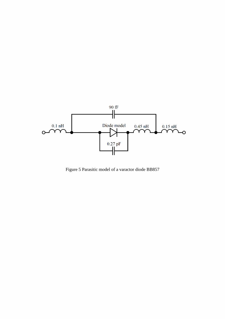
Figure 5 Parasitic model of a varactor diode BB857
a)
b)
Figure 6 Simulated scattering parameters of the Wilkinson divider/combiner when
applying a reverse bias voltage of a) 0V and b) 25 V
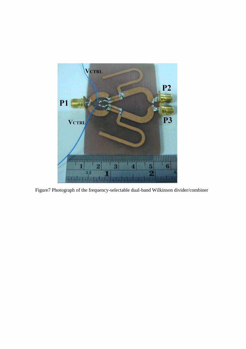
Figure7 Photograph of the frequency-selectable dual-band Wilkinson divider/combiner
a)
b)
Figure 8. Measured amplitude, input matching and isolation responses of the Wilkinson
circuit when the reversed bias is applied at a) 0 and b) 25 V.
a)
b)
Figure9. Phase balance of the Wilkinson circuit when applying the reversed bias
voltage, a) 0 and b) 25 V