Frequency Response and Gain Enhancement of Solid-State ...
212
Brigham Young University Brigham Young University BYU ScholarsArchive BYU ScholarsArchive Theses and Dissertations 2010-02-23 Frequency Response and Gain Enhancement of Solid-State Frequency Response and Gain Enhancement of Solid-State Impact-Ionization Multipliers (SIMs) Impact-Ionization Multipliers (SIMs) Joshua L. Beutler Brigham Young University - Provo Follow this and additional works at: https://scholarsarchive.byu.edu/etd Part of the Electrical and Computer Engineering Commons BYU ScholarsArchive Citation BYU ScholarsArchive Citation Beutler, Joshua L., "Frequency Response and Gain Enhancement of Solid-State Impact-Ionization Multipliers (SIMs)" (2010). Theses and Dissertations. 2001. https://scholarsarchive.byu.edu/etd/2001 This Dissertation is brought to you for free and open access by BYU ScholarsArchive. It has been accepted for inclusion in Theses and Dissertations by an authorized administrator of BYU ScholarsArchive. For more information, please contact [email protected], [email protected].
Transcript of Frequency Response and Gain Enhancement of Solid-State ...

Brigham Young University Brigham Young University
BYU ScholarsArchive BYU ScholarsArchive
Theses and Dissertations
2010-02-23
Frequency Response and Gain Enhancement of Solid-State Frequency Response and Gain Enhancement of Solid-State
Impact-Ionization Multipliers (SIMs) Impact-Ionization Multipliers (SIMs)
Joshua L. Beutler Brigham Young University - Provo
Follow this and additional works at: https://scholarsarchive.byu.edu/etd
Part of the Electrical and Computer Engineering Commons
BYU ScholarsArchive Citation BYU ScholarsArchive Citation Beutler, Joshua L., "Frequency Response and Gain Enhancement of Solid-State Impact-Ionization Multipliers (SIMs)" (2010). Theses and Dissertations. 2001. https://scholarsarchive.byu.edu/etd/2001
This Dissertation is brought to you for free and open access by BYU ScholarsArchive. It has been accepted for inclusion in Theses and Dissertations by an authorized administrator of BYU ScholarsArchive. For more information, please contact [email protected], [email protected].

Frequency Response and Gain Enhancement of Solid-state
Impact-ionization Multipliers (SIMs)
Joshua L. Beutler
A dissertation submitted to the faculty of Brigham Young University
in partial fulfillment of the requirements for the degree of
Doctor of Philosophy
Aaron R. Hawkins, Chair Gregory P. Nordin
Richard H. Selfridge Stephen M. Schultz
Robert C. Davis
Department of Electrical and Computer Engineering
Brigham Young University
April 2010
Copyright © 2010 Joshua L. Beutler
All Rights Reserved


ABSTRACT
Frequency Response and Gain Enhancement of Solid-state
Impact-ionization Multipliers (SIMs)
Joshua L. Beutler
Department of Electrical and Computer Engineering
Doctor of Philosophy
A study of the frequency response and gain of Solid-state the Impact-ionization Multiplier (SIM). The SIM generates current gain via impact ionization also known as avalanche gain. The SIM provides low noise amplification from an arbitrary current source. In the case of this study, current sources consisted of photodiodes optimized for a particular wavelength of light.
The SIM is fabricated from silicon and enjoys the low noise, low carrier transit time
advantages of conventional silicon impact ionization devices while amplifying current from a photodiode of a different material. This is advantageous because ideal detection and multiplication regions cannot always be grown on the same wafer. Furthermore a photodiode fitted to a SIM allows absorption and multiplication regions to be independently optimized.
The SIM exhibits a current dependant input resistance. This resistance in combination
with field effects from the SIM collector is the limiting factor in the frequency response of the SIM. Frequency response is improved to the extent that this floating voltage at the input can be minimized.
Higher AC gains are realized in the device with the incorporation of 3-dimensional
geometries. These improvements allow for improved device breakdown and reduced space-charge resistance at high input currents.
Frequency response can also be improved by increasing the current flowing into the SIM, this current is most often in the form of DC current such that it can be filtered off at a the output and not interfere with the input signal. Keywords: Joshua L. Beutler, impact ionization, solid-state, multiplication gain, frequency response, avalanche gain, SIM


ACKNOWLEDGMENTS
I would like to thank my advisor, Dr. Aaron R. Hawkins, for his support in this project.
We have spent many years researching together, and he has been a most helpful mentor and
teacher. I have learned tremendously from him. He has been an example of perseverance during
difficult times, and an immeasurable help in my education. His work at building up the
Integrated Microfabrication Laboratory (IML) and securing funding for its operation is a most
impressive achievement. The new lab equipment that he and Dr. Gregory P. Nordin have
introduced to the IML has greatly enhanced SIM fabrication techniques.
I would like to thank my committee members, Drs. Nordin, Richard H. Selfridge,
Stephen M. Schultz, and Robert C. Davis for their time and attention spent on this work. I have
taken classes from each of them, and greatly value the fundamental frameworks they taught
which provided a better physical understanding of the world around us. I would particularly like
to thank Dr. Nordin for allowing me access to the Chemical Mechanical Polisher and Dr.
Selfridge and Dr. Schultz for allowing me use of their variable gain high speed transimpedance
amplifier. Access to these resources was fundamental to writing several chapters of this
dissertation. Dr. Davis has been most encouraging with his advice and offered a physicist’s view
of semiconductor physics which has aided in double checking theories and ideas on this project.
I also thank my research friends and colleagues. Don Dawson and Joe Bussio in the shop
have been most helpful and free with their knowledge, time, and expertise. I appreciate Jim
Fraser’s excellent work in the cleanroom and have really enjoyed being able to bounce ideas off
of him. Michael Johnson has been most helpful with ideas, simulations, and packaging support


on this project. Josh Kvavle was most instrumental in getting me started in research many years
ago as well as helping me secure post-graduate employment.
I thank my family: my father who first encouraged me to get a PhD, my mother who
always knew I could, and most importantly my wife (who oversaw the complete editing and
formatting of this work) and three boys whose cheery smiles and joyous laughter so often lifted
my spirits after a long day of work. They have sacrificed with me as I have pursued additional
schooling.
I gratefully acknowledge financial support for this research through the Raytheon Ideas
Program and from the Defense Advanced Research Projects Agency through grant number
NBCHC050160, directed by Raymond Balcerak. Further research has been made possible
through funding from the National Science Foundation, Grant ECS-0700820.

TABLE OF CONTENTS
LIST OF TABLES ..................................................................................................................... xiii
LIST OF FIGURES .................................................................................................................... xv
1 INTRODUCTION ................................................................................................................. 1
1.1 Introduction ..................................................................................................................... 1
2 CURRENT OPTICAL DETECTORS ................................................................................ 5
2.1 Introduction ..................................................................................................................... 5
2.2 The Photomultiplier Tube ............................................................................................... 5
2.3 The PIN Photodiode ........................................................................................................ 9
2.4 The Avalanche Photodiode ........................................................................................... 12
2.5 Single Photon Counting APDs ..................................................................................... 15
2.6 Limitations of Existing Optical Receivers .................................................................... 18
2.7 The SIM: A Standalone Impact Ionization Amplifier .................................................. 22
2.8 Dissertation Overview .................................................................................................. 23
3 THEORY OF IMPACT IONIZATION ............................................................................ 25
3.1 Introduction ................................................................................................................... 25
3.2 Impact Ionization Gain Mechanism .............................................................................. 25
3.3 Ionization Threshold Energy ........................................................................................ 27
3.4 Ionization Coefficients and Gain Equations ................................................................. 30
3.5 Ionization Coefficient Measurement in Silicon ............................................................ 36
3.6 Impact-Ionization Response Time ................................................................................ 40
3.7 Multiplication Noise ..................................................................................................... 43
3.8 Conclusion .................................................................................................................... 47
4 FUNDAMENTALS OF THE SIM .................................................................................... 49
ix

4.1 Introduction ................................................................................................................... 49
4.2 Current and Voltage (IV) Characteristics of SIMs ....................................................... 50
4.2.1 Region A ................................................................................................................... 55
4.2.2 Region B ................................................................................................................... 57
4.2.3 Region C ................................................................................................................... 59
4.3 SIM Circuit Model and RC Frequency Response Limits ............................................. 61
4.4 Metal-Semiconductor Barrier Resistance and Space Charge Resistance ..................... 66
4.5 Frequency Response Measurement .............................................................................. 72
4.6 Conclusion .................................................................................................................... 76
5 OHMIC CONTACT INJECTION NODE SECOND GENERATION SIMS ............... 77
5.1 Introduction ................................................................................................................... 77
5.2 Ohmic Contact Electron Injection ................................................................................ 78
5.3 Similarities and Differences Between the SIM, MOSFET and BJT ............................ 80
5.4 Second Generation Frequency Response ...................................................................... 81
5.5 Fabrication and Testing ................................................................................................ 86
5.6 Device Operation .......................................................................................................... 88
5.6.1 IV Characteristics ...................................................................................................... 88
5.6.2 Gain Control .............................................................................................................. 89
5.7 Space Charge Factor ..................................................................................................... 91
5.8 Conclusion .................................................................................................................... 94
6 GAIN SHAPING VIA BURIED OXIDE .......................................................................... 95
6.1 Introduction ................................................................................................................... 95
6.2 Electron Confinement ................................................................................................... 96
6.3 Impact Ionization Efficiency ........................................................................................ 98
6.4 Benefits of Buried Oxide for Increased Ionization Efficiency ................................... 103
x

6.5 Buried Oxide Device Fabrication ............................................................................... 107
6.6 Gain Measurements .................................................................................................... 112
6.7 A Note on Metallization ............................................................................................. 114
6.8 The Importance of SU-8 in Planarization ................................................................... 116
6.9 Layout Compensation when Considering the KOH Etch ........................................... 117
6.10 Conclusion .................................................................................................................. 120
7 KEY ELEMENTS CRITIAL TO HIGH GAIN ............................................................ 123
7.1 Introduction ................................................................................................................. 123
7.2 Breakdown Voltage and Edge Effects ........................................................................ 124
7.3 Breakdown Voltages in the SIM and Their Effect on Gain ........................................ 127
7.4 Fabrication .................................................................................................................. 134
7.5 I-V Characteristics and Gain ....................................................................................... 135
7.6 Conclusion .................................................................................................................. 138
8 SIM FREQUENCY RESPONSE AND BARRIER LOWERING IMPLICATIONS 141
8.1 Introduction ................................................................................................................. 141
8.2 Floating Node Voltage Revisited ................................................................................ 142
8.3 Mixed Current Injection in an Ideal Diode ................................................................. 143
8.4 Mixed Current Injection in the SIM ........................................................................... 147
8.5 Mixed Input Frequency Response Measurement ........................................................ 152
8.6 Collector Induced Effects ........................................................................................... 153
8.7 Elimination of Collector Induced Effects on the Input ............................................... 159
8.8 P-Jacket Acceptor Concentration ................................................................................ 162
8.9 Conclusion .................................................................................................................. 163
9 CONCLUSION ................................................................................................................. 165
9.1 Introduction ................................................................................................................. 165
xi

9.2 Future SIM Work ........................................................................................................ 165
9.2.1 Substrate Current Injection ..................................................................................... 165
9.2.2 Resonant Tunneling Injection ................................................................................. 167
9.2.3 Noise and Sensitivity .............................................................................................. 168
9.3 SIM Applications ........................................................................................................ 169
9.4 Conclusion .................................................................................................................. 171
10 REFERENCES .................................................................................................................. 173
LIST OF PUBLICATIONS ..................................................................................................... 178
A APPENDIX A. Fabrication PROCEDURES ............................................................... 179
A.1 SIM Fabrication Procedure for Rectangular Buried Oxide SIMs ............................... 179
A.1.1 Step 1—KOH Etch Mask, and KOH Etching ......................................................... 179
A.1.2 Step 2—Oxide Growth and Diffusion Mask Planarization .................................... 181
A.1.3 Step 3—Diffusion ................................................................................................... 182
A.1.4 Step 4—Metallization ............................................................................................. 183
A.2 SIM Fabrication Procedure for Circular Pedestal SIMs ............................................. 184
A.2.1 Step 1—RIE, ICP Etching ...................................................................................... 184
A.2.2 Step 2—Oxide Growth and Diffusion Mask Planarization .................................... 185
A.2.3 Step 3—Diffusion ................................................................................................... 186
A.2.4 Step 4—Metallization ............................................................................................. 187
A.3 SIM Process Charts ..................................................................................................... 189
xii

LIST OF TABLES
Table 2.1: Photomultiplier Tube Materials [1] ............................................................................... 8
Table 5.1: Comparison of frequency limit of the Schottky contact SIM to that of the pn junction SIM. ....................................................................................................................... 86
xiii

xiv

LIST OF FIGURES
Figure 2.1: Illustration of the rudimentary components and electron action within a photomultiplier tube. ............................................................................................................. 6
Figure 2.2: a) A cross-sectional view of a PIN photodiode where light (hv) induced electron hole pairs are swept from the depletion region due to that presence of a fairly uniform field. b) Electric field magnitude in the PIN plotted against distance (Y) into the PIN. ... 11
Figure 2.3: a) A cross-sectional view of a Reach-Through Avalanche Photodiode (APD) where light (hv) induced holes are swept from the depletion region due to the presence of a fairly uniform field. That same field draws electrons into a high field impact-ionization region producing gain. b) Electric field magnitude in the APD plotted against distance (Y). ............................................................................................................ 14
Figure 3.1: Impact ionization in a high field region where electrons are the principle ionizers. . 26
Figure 3.2: The silicon band structure which illustrates the indirect nature of the valence and conduction bands [2]. .......................................................................................................... 29
Figure 3.3: An ideal slab of semiconductor medium with uniform electric field, a width (W) larger than 1 micron. This slab illustrates the current increases of electrons (Jn) and holes (Jp) as they traverse the impact ionization region. .................................................... 32
Figure3.4: Multiplication gain M versus multiplication length for pure electron injection for various α/β values are used to demonstrate its effect on the avalanche breakdown curve [3]. ....................................................................................................................................... 35
Figure 3.5: Measurement of pure electron injection and impact ionization in a PIN photodiode to accurately measure ionization coefficients under different fields. .................................. 38
Figure 3.6: These figures illustrate the time difference for a small ionization event to completely traverse the depletion region where a) only electrons cause ionization events and b) where electrons and holes are equally likely to cause ionization events. ................ 41
Figure 3.7: Avalanche multiplication 3dB frequency response limits due to differences in ionization coefficients of electron and holes [4]. ................................................................ 42
Figure 3.8: Excess noise factor as a function of gain for multiplication regions with varying ratios of ionization coefficients [5]. .................................................................................... 44
Figure 3.9: The multiplication region of an I2E avalanche photodiode. By engineering the bandgap across the multiplication, excess noise is deterministically inhibited as secondary holes drift through progressively larger bandgap materials [6]. ........................ 45
Figure 4.1: First generation vertical SIM structure. This cross-sectional view of a device shows a P type epitaxial layer on a P+ substrate. The electron collector is the N+ doped region and the hole sink is the P+ doped substrate. ............................................................ 53
xv

Figure 4.2: Graph showing Isim versus Vsim for a vertical device built using a P type epitaxial layer on a P+ substrate. An illuminated silicon photodiode served to inject current into the SIM. ........................................................................................................... 53
Figure 4.3: Representation of a model SIM current versus voltage curve with the 3 regions of interest labeled for discussion. ............................................................................................ 54
Figure 4.4: Representation of carrier action in the SIM when operating in region A. (a) Carrier action and semiconductor depletion in a cross-section of a vertical SIM. (b) Band diagram representation of the metal semiconductor interface and carrier action. ..... 56
Figure 4.5: Representation of carrier action in the SIM when operating in region B. (a) Carrier action and semiconductor depletion in a cross-section of a vertical SIM. (b) Band diagram representation of the metal semiconductor interface and carrier action. ..... 58
Figure 4.6: Representation of carrier action and semiconductor depletion in a cross-section of a vertical SIM when operated in region C. .......................................................................... 60
Figure 4.7: Circuit model for a SIM connected to a photodiode current source when Vsim is greater than the depletion voltage. I3 represents the impact ionization gain mechanism dependent current source. .................................................................................................... 63
Figure 4.8: Energy band diagram showing the barrier for electrons injected from a metal contact into a SIM built on a P type epitaxial layer. After the P type semiconductor between the metal and N+ semiconductor is completely depleted, raising Vsim by ΔV will lower the barrier Θbi by ΔΘ as shown. ......................................................................... 67
Figure 4.9: Electric field versus position in the depleted region between metal-semiconductor contact and electron collector. As Vsim increases, the slope of the electric field (-qNA/εs) remains constant and W decreases. ....................................................................... 68
Figure 4.10: Rbarrier + Rsc resistance versus input current between the metal-semiconductor and electron collector. The theoretical curve is calculated using (4.13) and (4.14) assuming a vertical SIM device made using a P type epitaxial layer, Schottky injection contact, and a spacing d equal to 4 microns. Measured values correspond to fabricated SIM devices with those parameters. .................................................................................... 72
Figure 4.11: Test setup used to measure the frequency response of SIM devices. ....................... 74
Figure 4.12: 3dB frequency response versus injected input current. Theoretical values were generated from equation 4.15 and measured values come from measurements on the same SIM device used to generate figure 4.11(P type semiconductor with Schottky injection). ............................................................................................................................. 75
Figure 5.1: Illustration of an ohmic contact. This contact is used on the injection node of the second generation SIM to effectively inject electrons into the semiconductor. .................. 78
xvi

Figure 5.2: a) Cross section of the SIM showing the geometries and doping. b) Illustration of field profiles in the area of the horizontal cutline shown in figure 5.2a when VSIM is 50 volts and the injected current is 1 uA. c) Illustration of the field profiles for the vertical cutline in figure 5.2a under the same conditions as previously mentioned. Electric field lines were extracted from ATLAS simulations of the structure. ......................................... 79
Figure 5.3: The difference in the conduction band structures of the a) Schottky contact SIM and b) the ohmic contact SIM. While the input resistance caused by the Schottky contact is eliminated, the built in voltage Θbi moves to the transition between the N+ doped region and the p- epitaxial region between the injection node and the collector. .... 83
Figure 5.4: Simulation of floating voltage at the input electrode for a range of input currents with 50 volts bias on the collector and the input being treated as a current source. Voltage values were extracted from ATLAS simulations of the structure shown in figure 5.2a. ........................................................................................................................... 85
Figure 5.5: Measured 3dB bandwidth for the fabricated SIM, represented by the diamond points, over a range of current levels. The theoretical response predicted by Eq. 5 is shown as a solid line, with 20 pF used for the node capacitance. A bias of approx. 40 volts was used. ..................................................................................................................... 88
Figure 5.6: a) Collector current versus voltage for modeled and fabricated pn junction injection SIMs. The solid black and gray curves represent simulated injection currents of 50 nA and 500 nA respectively. These are plotted along side test results for 50 nA and 500 nA injection which are represented by diamond and triangle plots respectively. The leakage current curve for the fabricated devices is also shown and is represented by the x’s. The fabricated device had a width of 10 μm between the n-wells of the injection and output nodes. b) Gain (M) versus voltage curve for the same modeled and fabricated pn junction injection SIM devices from a). ........................................................ 90
Figure 5.7: Top view of the first generation SIM. With a 3 x 1.5 µm Schottky contact and a 10 x 10 µm Phosphorous doped well electron collection. The length between the Schottky contact and n+ region is varied between 3 and 9 µm for different device designs on the same substrate. ............................................................................................. 93
Figure 5.8: Illustration of the SIM showing the injection pn junction and collector pn junction. The collector pn junction is biased to produce a depletion region and the cross sectional area used to determine space charge resistance is illustrated. ............................................. 93
Figure 6.6.1: Cross section of the ohmic contact SIM with Vsim=50V. Notice that the peak electric field resides at the corner of the N+ doping region roughly a distance D¬well from the SIM surface. .......................................................................................................... 97
Figure 6.6.2: Cross section of the ohmic contact SIM with Vsim=85V and Iinjection=10μA. The current density represents injected electrons moving from right to left close to the surface of the SIM, and hole density primarily generated via impact-ionization being drawn from the left N+ doped well toward the P+ substrate. ............................................. 97
xvii

Figure 6.6.3: Theoretical gain vs. voltage (M vs. V) plot as produced by equation 6.5 showing how the gain curves rise very abruptly with a low electron injection efficiency. It compares the theoretical cases of 1% efficiency for electron injection into the high field region and 100% efficiency. .............................................................................................. 101
Figure 6.6.4: ATLAS simulations showing the gain vs. voltage curves for Dwell=0.5μm, 1.5μm, and 3.0μm. It illustrates how the impact ionization efficiency is dependent upon the depth of the n+ well (Dwell). This is due to the electric field distribution for varied well depths. It becomes apparent that achieving appreciable gains is very difficult in devices with low impact ionization efficiency. ................................................................. 102
Figure 7.1: Cross sectional planar diffusion or implantation side profile junction. A junction curvature rj is formed at the edges of the doped regions. .................................................. 124
Figure 7.2: Illustration of an N-Well planar diffusion profile where the darkened area shows a) spherical regions and b) cylindrical regions. ................................................................. 126
Figure 7.3: Breakdown voltage Vb vs substrate impurity concentration, Nb, for plane, cylindrical, and spherical junctions for different radii of curvature [7]. ........................... 128
Figure 7.4: 3D cross-section of an avalanche photodiode (APD). Electron hole pair generation occurs in the absorption region after which a current undergoes impact-ionization in the multiplication region and collected. Notice contoured doping of the collection well and floating guard ring to confine carrier to the high field region and prevent breakdown. ........................................................................................................... 128
Figure 7.5: Illustrating different junction geometries to improve cross-sectional gain efficiency and reduce fields which create premature device breakdown. ......................... 130
Figure 7.6: Electric field magnitude looking down at the SIM. The highest field is at the corners of the collector causing most carriers moving from the input to the collector to miss the highest field region. ............................................................................................. 132
Figure 7.7: A circular geometry is necessary to confine electrons and fields in such a way to enhance gain efficiency and prevent premature device breakdown in the lateral plane. The pedestal in turn confines electrons and fields to provide the same benefits in the cross-sectional plane. ........................................................................................................ 133
Figure 7.8: Top view of a circular pedestal fields. Notice the uniformity of the maximum fields between the collector (outside ring) and input (inside ring). .................................. 133
Figure 7.9: Fabrication of the circular pedestal SIM begins by spinning a) SU-8 2002 on the wafer and b) patterning the active regions of the SIM. The resist allows for the formation of the pedestal by protecting the active region during the c) anisotropic etch to create the circular collector pedestal and ring input. d) The SU-8 is then removed and e) thermal oxide is grown over the entire wafer. f) SU8 is then placed over the wafer to protect the field oxide during polishing and g) the oxide on the top of the pedestal is removed via Chemical Mechanical Polishing (CMP). After cleaning off the
xviii

SU8, g) the exposed silicon pedestal tops are then doped with phosphorus spin on glass with the thermal oxide acting as a diffusion barrier. j) Lastly the spin on glass is removed and metal is patterned onto the doped pedestals. ............................................... 135
Figure 7.10: Current vs. voltage curve illustrating breakdown for different regions of a planar diode. ................................................................................................................................. 136
Figure 7.11: DC gain for Rectangular and Circular Pedestal SIMs. Circular pedestals exhibit higher controllable gains. .................................................................................................. 138
Figure 8.1: IV curve for the forward biased input node on the SIM. As input current, Iin, changes the voltage at the input Vinput must also change. Since the inverse of the slope represents resistance, the resistance at low input currents is quite large. .......................... 143
Figure 8.2: The IV curve of a diode biased with a large DC current to a setpoint. At that setpoint a small change in current causes a linear change in voltage such that the resistance seen by the small signal is constant and determined by the large DC current. 145
Figure 8.3: Conduction band diagram of the SIM under bias with injected electrons changing the high field region and thus altering the quasi-Fermi level at the input. ........................ 148
Figure 8.4: Response time τ, of the SIM for various changes in current ε, for values of I2 which are practically attainable in SIM operation. Capacitance used in this figure is 1.5 pF. ...................................................................................................................................... 151
Figure 8.5: The small signal response time for a system with small current signals no larger than one tenth the DC current signal. The resistance seen by the small signal is set by the DC current. Capacitance = 1.5 pF. ............................................................................. 151
Figure 8.6: The SIM Test Chip setup with bias-tee and TIA. The R and C values on the SIM Test Chip are used to filter the DC photiodiode bias and are R = 100 Ω and C = 200 nF in value respectively. ......................................................................................................... 153
Figure 8.7: Measured and theoretical 3 dB frequency response vs. change in input current 1 uA and 100 nA DC input currents. The theoretical model is the mixed current model in equation 8.25. .................................................................................................................... 154
Figure 8.8: As bias is applied to the SIM collector, the frequency response of the device drops. ................................................................................................................................. 156
Figure 8.9: Testing setup using an Agilent 4159 Semiconductor Parameter Analyzer to discover a collector induced voltage swing at the input. ................................................... 156
Figure 8.10: Measured change in voltage vs. current at the input of the SIM due to changes in collector potential. ............................................................................................................. 157
Figure 8.11: Simulated change in voltage vs. current at the input of the SIM due to changes in collector potential from SILVACO. Substrate doping concentration 1e14 cm-3. ........... 158
xix

xx
Figure 8.12: SIM input resistance and corresponding input current for collector voltages of 0, 20, and 40 volts. The theory line represents the theoretical kT/I resistance of the junction. ............................................................................................................................. 159
Figure 8.13: A surface SIM that potentially resists barrier lowering due to the collector at the input. a) The P+ doptant acting as a jacket around the n-well input b) keeps the built in voltage θbi from being affected by changes in the collector voltage. c) Simulated input current vs. input voltage in Silvaco for the structure seen in a). ....................................... 161
Figure 9.9.1: SIM where electrons are injected from the substrate. ........................................... 166
Figure 9.9.2: Two SIMs pre amplify current generated from a microphone before amplification in a summing amplifier. .............................................................................. 170
Figure A.1: SIM Oxide Growth Chart #1: This chart shows the necessary step gas flows, step temperatures, and step durations to grow roughly 1200 angstroms of thermal oxide to act as a KOH etch mask in subsequent steps. The low temperature provides the necessary oxide grow while minimizing the amount of diffusion within the EPI layer. .. 189
Figure A.2: SIM Oxide Growth Chart #2: This chart shows the necessary step gas flows, step temperatures, and step durations to grow 5000 angstroms of thermal oxide. This oxide acts as an insulator and passivation layer for the SIM. ..................................................... 190
Figure A.3: SIM Diffusion Chart #1 for P-8545 Spin on Dopant (SOD): This chart shows the necessary step gas flows, step temperatures, and step durations to diffuse phosphorus into the SIM pedestals to a depth of roughly 1.3 um. It is important that sufficient oxygen is always flowing into the furnace during the diffusion. Oxygen allows the phosphorus in the SOD to diffuse by turning the phosphoric acid (H3PO4) within the mixture into Phosphorus Pentoxide (P2O5). It is important to completely oxidize all the H3PO4 within the SOD otherwise it will form a bond with the silicon that cannot be removed unless it is first oxidized. Following diffusion, it is important to immediately dip the wafers in Buffered Oxide Etch (BOE) to completely remove the SOD before the P2O5 reacts with the moisture in the air to form H3PO4. ................................................... 191

1 INTRODUCTION
1.1 Introduction
In recent years, the number and scope of systems that utilize light collection as a primary
function of operation has grown appreciably. Applications which utilize Charge Coupled
Devices (CCD) [8] and Complimentary Metal Oxide Semiconductor (CMOS) sensors [9] have
not only changed the way people view photographs but revolutionized data acquisition and
mapping procedures in surveillance systems worldwide. Avalanche Photodiode (APD) arrays
collect and amplify small amounts of light from the cosmos to facilitate deeper probing into the
universe [10], while development of single photon detection systems create a method of key
distribution that is physically impossible to intercept. One key application in biophotonics can
resolve single molecules by bonding it to a fluorescing tag. Resolving the fluorescing signal
from this tag requires a sophisticated light collection system [11], but further realizes the allure
of mobile labs on a chip [12]. Perhaps no industry has benefited as much in the past two decades
from enhanced light collecting techniques than fiber optic networks which effectively make the
world smaller due to their multi-channel, gigabit speeds [13]. For each of these technologies
mentioned, there are many others whose function relies upon some form of light collection.
While some of these technologies do not operate at the extreme limit of optical detection, those
that do could significantly benefit from new, inexpensive forms of low noise current
amplification.
1

Low noise current amplification is not only desirable for technologies that involve light
collection. In reality, any detection technology which collects signals based on electrical current
could benefit from low noise current amplification. While all current based signals are
eventually amplified by transistor based amplifiers, different noise factors may limit their
performance. The limiting noise factor in a background noise limited detection system consists
of the current signal from the detector which does not constitute part of the desired signal. In
such a case, the signal itself serves as the chief method of introducing noise into the system. If a
system is background noise limited, it cannot benefit from a low noise current amplifier because
signal and noise are equally amplified. If, however, the current source is sufficiently clean, the
primary noise limiting factor then becomes a fixed system noise located within the detection
system. A system noise limited detection scheme is commonplace in systems where current
from the detector is diminished to the extent that the signal is below the noise threshold of the
transistor based amplification circuitry of the system. This is fairly commonplace but not limited
to fiber optics where the narrow line width of the laser source and subsequent filters eliminate
most of the background noise.
Detection systems that suffer from a fixed system noise typically implement a low noise
preamplifier to amplify the signal above the noise threshold of the transistor based circuitry.
These low noise current amplifiers utilize the principle of impact ionization as found in
Avalanche Photodiodes (APDs) or secondary ion emission as found in photomultiplier tubes
(PMTs). Several factors inhibit some detection systems from benefiting from low noise current
amplification. APDs and PMTs are limited to amplifying current from light signals while many
noise limited systems rely in current based signals instead. In such a scenario a low noise current
amplifier needs to be matched to a non-optical detection component. In such a scenario the
2

multiplication region is all that would be needed as the preexisting current source would already
be optimized. The final factor is cost. If such an amplifier cannot be produced at a reasonable
price, other solutions to system noise will be implemented. In essence a new type of amplifier
built on the fundamental physics of other low noise amplification devices is needed.
In order for these hurdles to be overcome, detection and amplification regions must be
physically separated, and the relative cost of implementation must be low. Furthermore, such an
amplifier needs to be a stand-alone device that can accept current from any random source of
input no matter whether that current is generated optically or electrically. The relatively small
size necessary to utilize impact ionization is desirable over secondary emission, as its means of
internal, low noise gain. Utilization of standard fabrication techniques for simple integration
with current technologies is also desirable. This configuration of physically separate and
individually optimized detection and amplification devices has several advantages. Not only
does it allow for further flexibility of systems that already use impact ionization based
amplifiers, but also pave the way for new applications.
This dissertation investigates the possibilities of such an amplifier. The Solid-state
Impact-ionization Multiplier (SIM) is a stand alone amplifier that utilizes impact ionization as its
primary means of current multiplication. The primary purpose of its development is to improve
and enhance current and light collection technologies via low noise pre-amplification.
3

4

2 CURRENT OPTICAL DETECTORS
2.1 Introduction
Before discussing the SIM in detail, several of the current technologies which are used in
light collection today will be explained to provide a better understanding of current technology.
Thus fostering a greater appreciation for the role the SIM seeks to play to improve upon existing,
mature technologies.
2.2 The Photomultiplier Tube
A Photomultiplier Tube (PMT) is a vacuum tube technology still widely used today. The
extreme sensitivity, broad spectrum responsivity, and configurable spatial resolution make it
widely used today in, fluorescence detection [14], astronomy [15], and single photon counting
[16].
Figure 2.1 shows a rudimentary cross sectional cut away of the basic PMT. Photons
enter the PMT through a faceplate or input window and strike a photocathode. Energy from
incident photons frees electrons from the photocathode by the photoelectric effect. These
electrons are then amplified as they strike a series of dynodes and free secondary electrons.
Primary and secondary electrons are finally collected for electrical measurement at the anode. A
high voltage power supply and resistor network provides the potential necessary for electron
amplification between the dynodes.
5

Most PMTs are biased to 1-2 kV and contain about 10 dynodes. Thus 100-200 volts are
dropped across each dynode. For every primary electron that strikes a single dynode,
approximately ten secondary electrons are generated. These high potentials produce electron
gains of roughly 106 and response times between 5 ns and 300 ps [1]. Thus the sensitivity and
response time of the PMT are of notable significance. A number of material variations in PMT
construction allow sensitivity to a broad spectrum of radiation. Variations in photocathode
material allow optimal sensitivity to radiation from 115 nm to 1200 nm. Depending on the light
source, different input window materials are selected for optimal transmission [17].
Figure 2.1: Illustration of the rudimentary components and electron action within a photomultiplier tube.
6
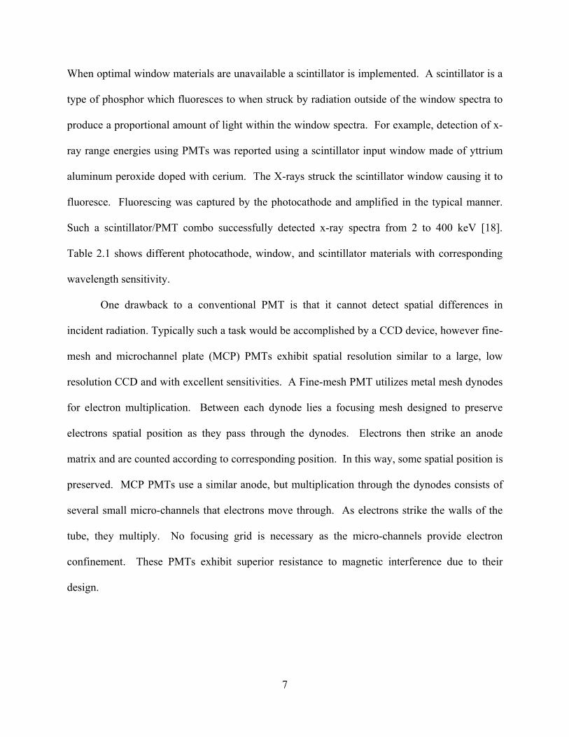
When optimal window materials are unavailable a scintillator is implemented. A scintillator is a
type of phosphor which fluoresces to when struck by radiation outside of the window spectra to
produce a proportional amount of light within the window spectra. For example, detection of x-
ray range energies using PMTs was reported using a scintillator input window made of yttrium
aluminum peroxide doped with cerium. The X-rays struck the scintillator window causing it to
fluoresce. Fluorescing was captured by the photocathode and amplified in the typical manner.
Such a scintillator/PMT combo successfully detected x-ray spectra from 2 to 400 keV [18].
Table 2.1 shows different photocathode, window, and scintillator materials with corresponding
wavelength sensitivity.
One drawback to a conventional PMT is that it cannot detect spatial differences in
incident radiation. Typically such a task would be accomplished by a CCD device, however fine-
mesh and microchannel plate (MCP) PMTs exhibit spatial resolution similar to a large, low
resolution CCD and with excellent sensitivities. A Fine-mesh PMT utilizes metal mesh dynodes
for electron multiplication. Between each dynode lies a focusing mesh designed to preserve
electrons spatial position as they pass through the dynodes. Electrons then strike an anode
matrix and are counted according to corresponding position. In this way, some spatial position is
preserved. MCP PMTs use a similar anode, but multiplication through the dynodes consists of
several small micro-channels that electrons move through. As electrons strike the walls of the
tube, they multiply. No focusing grid is necessary as the micro-channels provide electron
confinement. These PMTs exhibit superior resistance to magnetic interference due to their
design.
7
Despite their vacuum tube nature, PMTs satisfy numerous research and commercial
applications thanks to their sensitivity, response time, broad spectrum configurations, and newly
developed spatial detection.
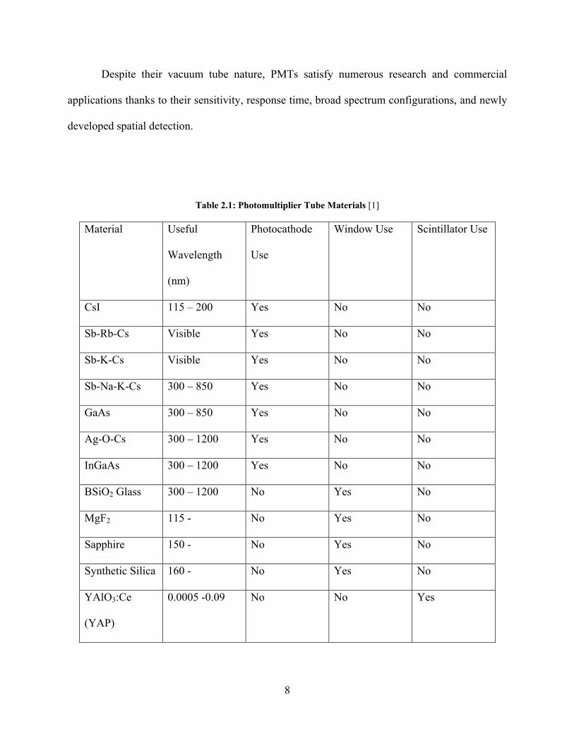
Table 2.1: Photomultiplier Tube Materials [1]
Material Useful
Wavelength
(nm)
Photocathode
Use
Window Use Scintillator Use
CsI 115 – 200 Yes No No
Sb-Rb-Cs Visible Yes No No
Sb-K-Cs Visible Yes No No
Sb-Na-K-Cs 300 – 850 Yes No No
GaAs 300 – 850 Yes No No
Ag-O-Cs 300 – 1200 Yes No No
InGaAs 300 – 1200 Yes No No
BSiO2 Glass 300 – 1200 No Yes No
MgF2 115 - No Yes No
Sapphire 150 - No Yes No
Synthetic Silica 160 - No Yes No
YAlO3:Ce
(YAP)
0.0005 -0.09 No No Yes
8

The signal to noise ratio of the PMT is given by Equation 2.1
2/)/4))(2(2 GRBkTFIIIqFB
INS
eqadbph
ph
+++= , 2.1
where Iph is the incident light, F the excess noise factor, B the bandwidth, G the mean gain, Ib is
the average photocathode current produced by background light, Id the dark current, and Fa the
amplifier noise figure. Since the PMT has such high gain, it is assumed that the amplifier noise
is negligible and hence not included [19].
PMTs also suffer from several drawbacks. The principle drawback is size. The smallest
are typically 1 inch in diameter. Such a measurement is of the tube itself and fails to include the
kilo-volt power supplies. While a microchannel plate helps to add limited spatial resolution, it is
still quite poor. PMTs are also quite slow in comparison to their solid state counterparts. This is
primarily due to the relatively large distance electrons must traverse through the dynodes. So
while PMTs exhibit the best sensitivity, of any detection device with internal gain, its bulky size
limits overall performance.
2.3 The PIN Photodiode
The PIN photodiode is the first solid state detector to be discussed in this chapter.
Furthermore, it is the only detector to be discussed without an internal gain mechanism. The
simple nature of the PIN photodiode makes it, perhaps, the most simple and robust of all light
collection devices. The PIN is a simple semiconductor PN junction optimized for responsivity,
speed and low noise.
A cross-sectional view of a PIN is illustrated in figure 2.2. The major change to the PN
junction is the inclusion of an intrinsic layer between the heavily doped p and n structures, hence
9

the name PIN. Light incident on the PIN creates electron hole pairs within the lightly doped
intrinsic region which is completely depleted with moderate bias. Electrons and hole are
separated by the field and are collected at the n and p type regions of the PIN. Doping the top of
the PIN with a heavily doped but thin n-type region improves responsivity by minimizing the
amount of light lost before it is collected in the depletion region. Further improvements to
responsivity require that all the light that enters the depletion region completely ionizes within
that region. This is accomplished by doping heavily next to the intrinsic region. The depletion
region formed at this junction combined with applied external bias creates a depletion region
sufficiently large to capture all incident light. Thus the introduction of an intrinsic region makes
the PIN as responsive as quantum efficiency will allow.
The intrinsic layer further enhances high speed optimization. Increasing the intrinsic
layer thickness effectively reduces the junction capacitance of the photodiode. Such a reduction
in capacitance can increase frequency response by changing the RC time constant. There is,
however, a trade-off. The wider depletion region increases the transit time of electrons and holes
through the depletion. Thus at high bit-rates an excessively wide depletion region will not allow
carriers from a first pulse of light to clear the depletion region before a second pulse arrives and
the two pulses will appear as one. However, an excessively narrow depletion region lacks
responsivity and suffers from poor bandwidth due to RC time constant limitations. The optimal
design requires depletion region transit time to be no more than half the modulation period of the
incident light [20]. This satisfactorily optimizes the RC and transit time factors without
considering effects on device responsivity.
10

Figure 2.2: a) A cross-sectional view of a PIN photodiode where light (hv) induced electron hole pairs are swept from the depletion region due to that presence of a fairly uniform field. b) Electric field magnitude in the PIN plotted against distance (Y) into the PIN.
PIN photodiodes exhibit low noise characteristics, the majority of which is due shot
noise. While leakage currents, background currents and actual signal currents contribute to
overall noise, the PIN, unlike all other devices discussed in this chapter, has no internal gain
mechanism and thus exhibits less noise than devices with an internal gain mechanism. The
Gain-Bandwidth product of a PIN photodiode is simply the bandwidth.
11

⎟⎠⎞⎜
⎝⎛
=
s
ddB
VW
fπ2
4.23 , 2.2
where Wd is the depletion region width, and Vs the saturation velocity of the electrons. The
signal to noise ratio can be seen below.
eqDBP
p
RkTBBIIIqI
NS
/4)(2
2
+++= , 2.3
where Ip is the signal generated current, IB the background current, ID the dark current, B the
bandwidth, and Req the equivalent resistance of the PIN and associated load resistors [20].
Factors that make the PIN advantageous are many. The relatively straightforward
optimization and innately low noise create a device that is easily fabricated with numerous
different semiconductor materials at relatively low cost. Consequently, the PIN photodiode is
often the detector of choice wherever system noise is not a limiting factor.
2.4 The Avalanche Photodiode
Avalanche Photodiodes (APDs) are a solid state form of photomultier tube in that a single
photon can cause the output of several electrons. APDs achieve this internal gain through a
series of impact ionization events known as avalanche gain. Years of research have improved
responsivity, speed, and noise of these devices such that these features, combined with excellent
gains, create an attractive device in situations where a fixed system noise is a limiting factor.
Creating an Avalanche Photodiode (APD) can be as simple as reverse biasing a PIN
photodiode until the electric field within a region of the PIN becomes large enough to allow free
carriers ionized by light to ionize other carriers from the semiconductor lattice. The overall
effect is internal current gain similar to a PMT but in a smaller package and via a different
12

physical mechanism. Device design greatly affects APD responsivity. Different APD structures
have been used through the years with fair success, but perhaps the most common and successful
is the Reach-Though APD. The Reach-Through APD is illustrated in figure 2.3. It sandwiches
an intrinsic semiconductor layer between a pn junction and heavily doped n or p type material.
Under high bias voltages, the field in the pn junction becomes sufficiently strong to create
impact-ionization events or avalanche multiplication. The field from the pn junction also needs
to be large enough to completely deplete the intrinsic portion of the device. In this way the field
“reaches through” to the other side of the APD thus making a large absorption region. Thus
design considerations can greatly affect the overall device responsivity.
Device design further affects the overall speed of the APD. While a wide depletion
region allows for a greater responsivity, too large a region increases the region carriers must
traverse and thus the frequency response becomes transit time limited. Significant attention must
be placed on doping and geometry to ensure that electric fields throughout the APD optimize
gain and transit time without creating premature device breakdown. If insufficient field drops
across the intrinsic region, carriers will not traverse the region at saturation velocity. In such a
situation, biasing the APD further may enhance the transit time only to cause premature
breakdown the multiplication region. While generation of secondary carriers via impact
ionization within the multiplication region of the APD also decreases the frequency response,
this is not readily evident until the gain-bandwidth of the APDs exceeds 100 GHz [5] and will be
treated in more detail in Chapter 2.
13

Figure 2.3: a) A cross-sectional view of a Reach-Through Avalanche Photodiode (APD) where light (hv) induced holes are swept from the depletion region due to the presence of a fairly uniform field. That same field draws electrons into a high field impact-ionization region producing gain. b) Electric field magnitude in the APD plotted against distance (Y).
Due to the nature of impact ionization, excess noise is introduced with each impact
ionization event. This excess noise is typical of all impact ionization events and contributes to
the overall noise of the system. Consequently, APDs are used in applications where the noise is
not limited by the detector, but rather by some set system noise such as a transistor based
amplifier. In such a case where the APD noise is small compared to noise generated in an
external amplifier, APDs can effectively amplify an otherwise lost input signal to a current level
14

above that of the amplifier. While conventional methods for calculating excess noise often over
estimate the actual noise generated by impact ionization in the APD [21], [22], they are fairly
accurate for larger depletion region devices and will be discussed in Chapter 2.
APDs satisfy an important need in measurement and detection systems by internally
amplifying light signals before conventional amplification. They do this in an efficient, fast, and
low noise manner with many similarities to PMTs but in a more compact, high-speed package.
2.5 Single Photon Counting APDs
Single photon counting constitutes to some extent the holy grail of optical detection
today. APDs and PMTs are useful in successfully detecting single photon events. However, the
presence of a single photon induced electron hole pair does not constitute sufficient current to be
detected in conventional APD or PMT schemes. Consequently the overall bit rate of these
devices suffers.
Detecting photons in an APD requires a current gain substantially larger than the gains of
10 to 100 that an APD biased in a conventional linear mode can provide. Higher gains are
extracted from devices by designing them to withstand over-biasing and still stay at a zero
current state for some microseconds to seconds before breakdown. This type of APD is known
as a Single Photon Avalanche Diode (SPAD). The state of over biasing that these diodes operate
in is known as Geiger mode operation. If a photon enters the SPAD during this time, it can set
off an ionization event and cause the diode to breakdown. It should be noted that the photon is
not itself detected, but merely the ionization event. The large ionization event produced would
be the same whether a single photon ionized or 10 photons ionized. Since other external factors
can cause a false ionization event, photon counting diodes are shielded and cooled to protect
15

against stray photon events and thermal fluctuations from triggering breakdown. After
breakdown is detected, the diode is then quenched. Quenching lowers the applied bias on the
diode to a voltage below breakdown. This allows the avalanche effect to die out and the diode to
establish a zero current level before it is over biased again. This time allowed for quenching
before re-biasing is called dead time. Any photon entering the SPAD during dead time has no
probability of being detected.
Even during Geiger mode operation, not every photon triggers an ionization event.
Device quantum efficiency limits the percentage of single photon events that successfully create
electron hole pairs. Furthermore, the probability that these electron hole pairs can create a chain
of ionizations sufficient to cause the whole diode to ionize is not guaranteed either. Other effects
of Geiger mode operation such as diode heating, dead time and afterpulsing further limit
performance of APDs optimized for single photon detection.
Diode heating is still a problem even on the cooled stages used in single photon detection
schemes. Thermal fluctuations sufficient to ionize carries within the depletion region of an APD
can cause false ionization events. These heat sources typically originate from the light source
and spread to subsequent areas from there. For example, incident photons may induce phonons
within the structure of the APD which may cause a false detection by thermally freeing carriers
which in turn further heat the diode. Proper mounting on heat sinks can significantly reduce the
amount of thermal energy capable of degrading device performance provided the packaging and
other mounting constraints of the APD provide a pathway low thermal resistance [23].
Dead time constitutes the amount of time required to quench an ionization event by
lowering the voltage below the breakdown voltage before the ionization event passes and the
APD can resume Geiger mode operation. In many cases, the quenching circuitry can influence
16

the dead time. Passive quenching circuits typically consist of a large resistor in series with the
SAPD. A large amount of current passing through the resistor causes more and more voltage to
drop across it. This effectively reduces the bias on the SAPD below breakdown and ensures that
the ionization event does not run away. As the ionization event subsides, the voltage is reapplied
according to the RC time constant of the system. Since the capacitance of the system is typically
dominated by the diode, the resistance is the only factor that easily modifies the dead time of the
system. The trade-off is that the larger resistance creates a larger voltage drop and thus a higher
photon electron counting efficiency in silicon SPADs whereas a smaller resistance allows for a
shorter dead time and therefore faster bit rate [23]. Active quenching circuits seek to drastically
lower the diode voltage as rapidly as possible once an ionization event is detected and then
quickly ramp up the voltage after the event passes. Consequently, if elimination of the trade-off
between counting efficiency and bit rate is desired, then active quenching circuits of most
desirable.
All these limitations imposed on diode performance would be of little consequence and
still allow for telecom bit rates were it not for afterpulsing. Afterpulsing results from carriers
that are trapped in shallow states that are later released due to thermal excitation. Naturally, the
thermal energy gained from an ionization event frees other carries which need to be fully
dispersed before recommencement of Geiger mode operation. In consequence, diode dead time
is increased as the afterpulsing carriers are allowed to diminish. Afterpulsing is proportional to
the population of traps in the material and the time constant that governs the length of the
afterpulsing only increases with lower temperature. This is most detrimental to performance of
telecom SPADs optimized for far-infared operation. InGaAs/InP photon counting APDs which
exhibit an operating frequency in the GHz range when operated below breakdown are only
17

capable of low MHz rates in Geiger mode operation. The InP in these photodiodes appeares to
house a significant number of traps as it’s absence significantly reduces afterpulsing. However,
afterpulsing was also decreased by adding several grading layers between the InGaAs and InP
band discontinuity. This discontinuity creates a barrier that is most ideal to trap a significant
number of carriers that can only be freed by thermal excitation [24]. While several active
biasing schemes are employed to milk the highest possible bit rate from these devices, they still
fall fairly short of conventional telecom standards in many ways [25]. Contrast this to silicon
SPADs which exhibit little or no afterpulsing. Consequently, silicon SPAD detection systems
are capable of GHz speeds. Unfortunately, silicon detectors cannot be employed in fiber-optic
communication systems due to their inability to detect far-infrared light.
The race to make better SPADs suitable for telecom is in somewhat of a quagmire. It
should be noted that as recently as 2008, reports on GHz Quantum Key Distribution (QKD)
using InGaAs APDs have been published. This is slightly misleading as it sounds like these
APDs operate at GHz speeds. In reality, they transmit the quantum key for a GHz speed fiber.
In a recent article, [26] Yuan reported a proof of principle 100 Kbps secure bit rate over a 40 km
fiber. Thus efforts to improve the overall detection setup have helped to negate some effects
such as diode heating. However, current methods to quench afterpulsing in such diodes leave a
significant material hurdle to reap the rewards of faster operation speeds.
2.6 Limitations of Existing Optical Receivers
The previous sections seek to give an overview of some devices used in light detection
that have similar detection or multiplication properties to the SIM. Each of these devices is
useful as evidenced by their commercial existence and physical properties. However, each
18

device has physical limitations that inhibit improvement in overall performance and confine
them to their current state of usefulness in optical detection. It should also be clear that a hybrid
of these devices would be a most useful and welcome addition.
PMTs detect small signals best thanks to their capacity for enormous gains. However,
they are large and bulky, limited in bandwidth and in many cases suffer from poor quantum
efficiency. Most PMTs exhibit a quantum efficiency of approximately 30% at optimized
wavelengths [27].
The success of SPADs, especially at telecom wavelengths, is primarily a material issue.
Until defects in III-V semiconductors can be significantly reduced or until new defect free
semiconductors can be developed that replace current III-V semiconductors, afterpulsing will
continue to plague quantum cryptography systems and confine them to MHz operations. On the
other hand silicon SPADs look quite promising.
PIN photodiodes are excellent performers in bandwidth. Their small size, simple design
and ability to be material wavelength optimized create a high speed, efficient device. However,
they are limited by amplifier noise. APDs remedy this problem by adding an internal
amplification medium to the PIN. This effectively gives the APD 10 to 15 dB greater sensitivity
than a PIN diode alone. However, the multiplication and detection layers are now physically
linked together in such a way that makes them interdependent. If there is any sad and
disappointing maxim in fabricating APDs it is this: Materials with good detection properties
typically exhibit less than ideal multiplication properties.
The converse is also usually true. Therefore optimization of absorption layer only occurs
at an increased cost to multiplication layers. This is often the case with APDs used in fiber-optic
networks. InGaAs absorption layers exhibit high quantum efficiency at 1500 to 1300 nm
19

wavelengths, however the small bandgap coupled with the overall material properties of InGaAs
make it a poor multiplication layer. This short coming is solved by epitaxial growth of a material
more suitable for impact-ionization multiplication onto the InGaAs absorption region. If any
material could be chosen then silicon would be the first choice. Silicon is in most instances is
less expensive, produces less excess noise during impact-ionization, and most ideal during
impact-ionization when compared to other materials.
Silicon is fairly straightforward and the least expensive of all epitaxial growth process.
Because silicon is monatomic, only one carrier gas is necessary for the reaction to properly
occur. The stoichiometry is simple and hence so is the crystal growth. Silicon is also readily
abundant for harvest all over the earth.
Silicon also exhibits the lowest excess noise factor of any semiconductor or superlattice
during impact ionization. As electrons and hole under go impact ionization a certain amount of
excess noise is generated for each event. The larger this noise, the smaller the Signal to Noise
Ratio (SNR) and the lower the sensitivity of the device. Silicon exhibits the least excess noise of
any semiconductor. Therefore utilization of silicon as a multiplication layer creates a most
sensitive APD.
Impact ionization is also the most ideal in silicon. Ideally, when electrons and holes enter
a high field and undergo impact ionization, single carrier multiplication is must desirable. In an
ideal case, an electron would ionize to create an electron-hole pair. The electron would travel
through the field until it gained enough kinetic energy to ionize another electron hole pair. On
the other hand, the holes would never reach ionization threshold energy. In silicon electrons are
20 times more likely to reach ionization thresholds than holes. This allows silicon to be treated
for the most part as an ideal impact ionization system. This single carrier ionization system
20

reduces the transit time of signals through the APD. Choosing another semiconductor for a
multiplication layer like InP would be less advantageous with regard to carrier multiplication. In
InP holes are more likely to ionize, but the difference between electron and hole ionization
probabilities is not nearly as large as silicon. This means that electron and holes ionize and in
turn create more electron-hole pairs that in turn continue the process. Instead of a swift march of
ionizing electrons across the multiplication, the equal probability of carrier ionization creates a
feedback mechanism that allows pulses to linger in the multiplication region. This increases
transit time and decreases the device bandwidth. So silicon is the multiplication layer of choice.
Unfortunately, silicon is not the multiplication layer of choice. The reason goes back to
the interconnectedness of absorption and multiplication layers in APDs. Silicon cannot be
epitaxially grown onto InGaAs, HgCdTe, InAs or any other III-V semiconductor because of a
large difference in the lattice constant of the two materials. Any attempt to do so would cause
strain induced defects at the interface between the two materials that would more than negate any
positive effects a silicon multiplication layer would provide to the device. Instead the material of
choice is InP because differing alloys of InGaAs or buffer layers between the absorption layer
and InP multiplication layer can be lattice matched. Thus, even though InP has a greater excess
noise factor and exhibits less than ideal carrier multiplication ratios, it is often the multiplication
layer of choice in telecom APDs. It should be noted that while techniques employing wafer-
bonding instead of epitaxial growth have sought to create APDs with silicon multiplication
layers and InGaAs absorption layers, no commercially viable devices have been made yet [28].
APDs also require that electrons travel through the same pathway as holes. In such cases
electrons may recombine with holes and thus quench current gain and cause recombination
noise. This is particularly a problem in multiplication regions with less than ideal carrier
21
multiplication ratios. It would be best if the multiplication region utilized all three dimensions of
space in the multiplication region. By so doing, fields could be biased to effectively separate
electrons from holes and prevent recombination.
The progress made on APDs over the last two decades has been most impressive. While
still somewhat of a niche market and made by only a handful of skilled companies, they have
made the APD a reliable, performance device used in a variety of applications. However, what
is lacking is the ability to optimize the impact ionization mechanism independently and without
consideration for the detection mechanism. The SIM seeks to bridge that gap.
2.7 The SIM: A Standalone Impact Ionization Amplifier
The Soild-state Impact-ionization Multiplier (SIM) seeks to act as a stand alone current
amplifier utilizing impact ionization. It is made of silicon and therefore possesses the previously
described attributes of such a material. It is also made using industry standard VLSI techniques
and machinery. Such a device proves advantageous because it accepts any arbitrary current
source. Thus ideally, any detector could be optimized without consideration for the amplifier
provided it produce a current. In the most practical of scenarios, this means that photodiodes
optimized for different wavelengths of light can be electrically wired to the SIM. The output
current from the photodiode is input into the SIM. Current injected into the SIM undergoes
impact ionization, and leaves the SIM amplified. Furthermore, output signals from each of these
photodiodes looks identical provided the inputs are identical. Thus, the SIM is not
discriminatory to different current sources. The viability of this device now depends of its ability
to perform similarly to APDs in other respects.
22

The purpose of this dissertation is to evaluate several parameters and important functions
of the SIM that have previously been unknown. These main aspects focus on improving the
internal gain of the SIM, optimizing frequency response, and improving space charge resistance.
Knowledge of these parameters will not only help to assess the commercial viability of the SIM,
but also provide a feel for general target applications.
2.8 Dissertation Overview
The SIM was created by Dr. Aaron Hawkins and his PhD student Hong-Wei Lee. The
first working SIM was documented in the summer of 2005. It was working in the sense that it
exhibited DC current gain when fed from a DC current source (a photodiode under constant
illumination). During the ensuing months and even year, much work was done to demonstrate
device operation, current gain impact ionization generated on the silicon surface or substrate, and
high gain effects through cascading several SIMs together. This work seeks to answer some of
the questions that, at that time, were yet to be answered but mostly hadn’t even been considered
by the conclusion of Hong-Wei’s dissertation. Chapter 2 has sought to give a rudimentary feel
for some existing optical detection devices and present a convincing need for a device like the
SIM. Chapter 3 deals with the history and theory of impact ionization including the gain
mechanism, impact ionization rate, excess noise, and the bandwidth. Chapter 4 covers the
original SIM device operation. The fundamental operation of the SIM will be outlined as well as
the first inquisition probing the frequency response of the SIM. Suggestions for an improved
SIM are also outlined. Chapter 5 introduces a second generation device that replaces the
Schottky metal injection node with an ohmic contact pn junction injection node. Chapter 6
discusses improved gain in second generation SIM devices by developing a Buried Oxide
23

structure. Chapter 7 further addresses geometrical issues in the SIMs architecture to improve AC
gain by eliminating premature device breakdown. Chapter 8 discusses frequency response of the
SIM with a mixed current input and setups to further improve frequency response as collector
induced field effects are minimized. Chapter 9 deals with future work and practical applications
of the current SIM.
24

3 THEORY OF IMPACT IONIZATION
3.1 Introduction
Impact ionization or avalanche breakdown as been observed and studied in
semiconductors since the 1950s [29]. However, as optoelectronic device designers envisioned
enormous benefit from avalanche breakdown, this phenomenon, which was once considered the
extreme limit of useful device performance, is the primary mechanism in the SIM. Hence the
original term of “avalanche breakdown” which signified the limit to device performance is also
known by many as “avalanche gain.” In this chapter the impact ionization mechanism behind
avalanche gain will be discussed as well as classical gain equations. Since impact ionization
occurs in most medium to large bandgap semiconductors, these equations are fairly general and
apply to this wide range of crystals. The parameters that fit this equation to the peculiarities and
unique qualities of each semiconductor are the ionization coefficients. These are unique to each
semiconductor. Their measurement and effect on device gain, excess noise, and bandwidth will
then be discussed.
3.2 Impact Ionization Gain Mechanism
When an electric field is applied to a semiconductor, free carriers within the
semiconductor gain energy and drift through the field. As they drift, they lose energy through
collisions with phonons, impurities, or defects. Under low fields, the energy imparted to carriers
25

by the field and the energy lost through collisions exhibit a check on each other. Thus the
carriers’ energy and lattice energy are in equilibrium. At high fields, this equilibrium decays as
carriers gain more energy from the field than they impart to the lattice through collisions until
they possess sufficient energy to free carriers from the lattice via impact ionization. This results
in the generation of a secondary electron and hole in the conduction band and valence band
respectively. While in the high field these secondary electron hole pairs also gain sufficient
energy to free other electrons from the valence band. As this process continues the number of
ionizing carriers rapidly increases causing avalanche breakdown. Figure 3.1 illustrates electron
impact-ionization.
Figure 3.1: Impact ionization in a high field region where electrons are the principle ionizers.
26

Typically, a fairly high field is needed to create ionization events. Naturally the bandgap
is of important consideration. The larger the bandgap the greater energy needed to free or excite
valence band electrons into the conduction band. In low bandgap materials such as InAs (Eg =
0.33 eV), a field of 104 V/cm is necessary. While large bandgap semiconductors such as GaP (Eg
= 2.24 eV) require far greater than 105 V/cm [30]. Silicon (Eg = 1.12 eV) requires a field of
roughly 1.2x10⁵ V/cm to breakdown. Thus a minimum ionization energy exists which has some
dependence on the semiconductor bandgap.
3.3 Ionization Threshold Energy
It seems fairly intuitive that the minimum energy required to excite an electron from the
valence band to the conduction band would simply be the energy of the bandgap. However, this
assumes a perfectly elastic collision where all energy from electron 1 is transferred to free
electron 2. Furthermore the secondary hole is also neglected. Thus a more comprehensive
model requires ionization energies greater than the bandgap. Even using the most simple
parabolic band structure the lowest threshold energy, Ei is greater than the bandgap. Consider
two parabolic bands consisting of a conduction band with effective mass me and a valance band
with effective mass mh. After an electron undergoes impact ionization, there are now three
particles. The original electron and secondary electron hole pair. Assuming the collision to be
elastic, conservation of energy and momentum show the minimum total energy required for an
electron to reach threshold is
)212
21(
21 222
hheegie vmvmEvm ×+×+= . 3.1
27

The momentum follows as
hheeieei vmvmvmP +×== 2, . 3.2
In the case that me = mh, and that the velocities of the secondary electron hole pair are equal (i.e.
ve = vh = vf), these equations can be further simplified such that
22
23
21
fegie vmEvm += 3.3
and
. 3.4 feie vmvm 3=
Substituting momentum into energy yields the famous 3/2 the bandgap ionization energy
explained by Wolff [31]
giei EvmE 5.121 2 == . 3.5
While this is a good rule of thumb for direct band semiconductors, it is a poor one for
indirect band semiconductors. In the case of silicon, the ionization energy is significantly higher
than the 3/2 bandgap rule. This, as Wolff surmised, has a great deal to do with the indirect
nature of silicon. The band structure of silicon is shown in figure 3.2 [2]. Because of silicon’s
indirect bandgap, conservation of crystalline momentum requires an indirect process to allow
transfer of electrons from the Г valley to the X valley. In such a case indirect mechanisms such
as the umklapp process, phonon absorption or other mechanism facilitate impact ionization.
These events in silicon require more energy than a simple parabolic direct band structure. Since
Wolff’s theoretical contributions, careful empirical measurements on silicon reveal a 2.6 eV
electron ionization energy and 5 eV hole ionization energy.
28

Figure 3.2: The silicon band structure which illustrates the indirect nature of the valence and conduction bands [2].
The disparity between electron and hole ionization energies makes silicon a most
advantageous material when designing a device based on avalanche gain, but still proves
somewhat of a theoretical mystery. While several theories exist which seek to explain electron
and hole ionization disparities, a unified encompassing theory is still missing. Consequently,
while a considerable amount of theoretical work has proved beneficial in explaining empirical
measurements, these models are often too confined and lack sufficient robustness to shed light
on physical attributes which have not yet been realized. For those desiring some explanation, a
fairly straightforward theoretical reason is due to a .1 eV separation between the intersections of
29

two conduction bands at the X valley minimum in silicon. This intersection significantly
increases the density of states within the conduction band. thus allowing for completion of more
indirect bandgap events by providing more open electron states [3]. Valence electrons can only
move to the conduction band provided that their energy and crystalline momentum matches an
unoccupied state within the conduction band. Provided that indirect factors such as electron
phonon interactions provide the indirect shift in crystalline momentum, the energy must still
match that of an unoccupied conduction band state. Thus while a 1 eV separation in two
conduction bands has no effect on crystalline momentum, it provides a significantly higher
probability that ionized electrons will find the necessary energy state within the conduction band
than ionized holes will in the valence band.
3.4 Ionization Coefficients and Gain Equations
The equations that describe impact ionization are quite similar for all semiconductors.
The principle difference is the value of the ionization coefficients. These coefficients denote a
probability of ionization. They are heavily dependent on electric field. The ionization
coefficient for electrons is defined as α, while the ionization coefficient for holes is β. The units
for α and β are in inverse length, typically cm-1. This unit denotes the reciprocal of average
distance an electron or hole must travel within a uniform field before ionizing a secondary
electron hole pair. After examining the units of these ionization coefficients and examining
many of the illustrations in the chapter, the reader may be lead to believe that impact ionization
is a deterministic and wholly predictable process in which each electron and hole involved in the
process have equal ionization potential. This is not true. The units of α and β denote the bulk
action of carriers and the illustrations are to convey an overall view of the mechanism. The
30

random nature of impact ionization is not carefully considered in classical impact ionization
equations. Thus they are of little use when predicting impact ionization events through a space
smaller than 1/ α or 1/β. Furthermore the robust nature of classical gain equations depends
greatly on uniform field distribution. In the case of the SIM and most APDs, the classical model
is sufficiently robust. However, in cases where classical conditions fail to adequately satisfy a
particular environment, the reader is directed to the of work of R. J. McIntyre and J.C. Campbell
[21],[22].
Classical impact ionization gain equations are best comprehended with the aid of a
simple model. This model will help illustrate the robustness and limitations of these equations.
Assume the medium to be a simple slab of lightly doped semiconductor of width, W on the order
of a micron or more. An electric field across the semiconductor creates a depletion region across
the slab. Further increase in that field creates a high field impact ionization region as well. The
field points from right to left and current flows to the left. Such a scenario is illustrated in figure
3.3. This model is virtually identical to the impact ionization region within a PIN photodiode
under high reverse bias, many APDs, and the SIM. With such a model in place, conservation of
current allows the formation a differential equation that describes the electron and hole current
density at any position x within the semiconductor. For electrons,
)()()()( xJxxJxdx
dJpn
n βα += 3.6
and for holes,
)()()()( xJxxJxdx
dJpn
p βα +=− . 3.7
These equations further assume that no current is generated in the depletion region from optical
generation of electron hole pairs. This constrains the current entry and exit points to the right
31

and left sides of the diode. Such as scenario is quite realistic in the case of the SIM and many
types of APDs. The SIM uses pure electron injection into a high field to create gain and in this
way no optical generation is required. The structure of some APDs such as those that implement
a Separate Absorption and Multiplication (SAM) structure enhance device performance by
injecting a single carrier into the multiplication region of the diode. So for many practical cases,
and especially for the case of the SIM, such an assumption is quite practical.
Figure 3.3: An ideal slab of semiconductor medium with uniform electric field, a width (W) larger than 1 micron. This slab illustrates the current increases of electrons (Jn) and holes (Jp) as they traverse the impact ionization region.
32

If we further assume a pure electron injection scenario like the SIM, it then follows that
Jp(W) = 0 and that
)()()( WJxJxJJ npn =+= . 3.8
Substituting this into the above differential equation for electron density, it becomes
)()()()()()(
WJxxJxxdx
xdJnn
n ββα =−− . 3.9
This is an ordinary differential equation and can be solved in typical fashion provided that the
integrating factor = ∫ −−x
dx0
]')(exp[ βα )](exp[ xφ− be used to take care of the α(x) and β(x)
functionalities. Using this integrating factor and integrating the length of the intrinsic region
from 0 to W, electron current density becomes
∫
∫ ∫
−−
+−−×= x
x x
nn
n
dxxx
JdxdxxxWJxxJ
0
0 0
]')'()'(exp[
)0(]')'()'(exp[)()()(
βα
βαβ. 3.10
Gain for pure electron injection is defined as )0(/)( nnn JLJM = . Thus,
∫ ∫∫ ⎥⎦
⎤⎢⎣
⎡−−−⎥
⎦
⎤⎢⎣
⎡−−
==W xW
n
nn
dxdxxxxdxxxJ
WJM
0 00
')'()'(exp)()()(exp
1)0()(
βαββα
. 3.11
Equation 3.11 can be further simplified using integration by parts ( )∫ ∫−= BdAABAdB on the
second term in the denominator. In this case
⎟⎟⎠
⎞⎜⎜⎝
⎛⎟⎟⎠
⎞⎜⎜⎝
⎛−=⎥
⎦
⎤⎢⎣
⎡−−− ∫∫∫ ∫
xxW x
dxxdxxdxdxxxx000 0
')'(exp')'(exp')'()'(exp)( βαβαβ
(A) (dB)
33

dxdxxdxxxdxxdxxxW xWxx
⎥⎦
⎤⎢⎣
⎡−⎥
⎦
⎤⎢⎣
⎡+
⎪⎭
⎪⎬⎫
⎪⎩
⎪⎨⎧
⎥⎦
⎤⎢⎣
⎡−⎥
⎦
⎤⎢⎣
⎡= ∫∫ ∫∫∫
00 0000
')'(exp')'(exp)(')'(exp')'(exp αβααβ
∫ ∫∫ ⎥⎦
⎤⎢⎣
⎡−−+−⎥
⎦
⎤⎢⎣
⎡−−=
W xW
dxdxxxxdxxx0 00
')'()'(exp)(1)()(exp βααβα . 3.12
In this fashion the final expression for electron injection gain is derived as
∫ ∫ ⎥⎦
⎤⎢⎣
⎡−−−
=W xn
dxdxxxxM
0 0
')'()'((exp)(1
1
βαα. 3.13
The solution for hole injection is quite similar and shown here as
∫ ∫ ⎥⎦
⎤⎢⎣
⎡−−
=W W
x
p
dxdxxxxM
0
')'()'((exp)(1
1
βαβ. 3.14
In the case of the SIM, the gain equation for electron injection can be further simplified provided
that α >>β and α be constant. The former is true for silicon while the latter depends on the
device structure. Since ionization coefficients are field dependent, further simplification of
equation 3.14 would only be of significant use if the field within the multiplication region is
uniform. The lightly doped EPI layer of the SIM provides a fairly uniform field. Under these
conditions,
( )[ ]
( )( ))(exp
)(exp)(
)(exp1
1
0βαβαβαβα
βαβα
α −−−−
=−−
−+
=WW
xM
Wn 3.15
and
( )[ ]
( )( ))(exp
)(exp)(
)(exp1
1
0αβαβαβαβ
αβαβ
β −−−−
=−−
−+
=WW
xM
Wp . 3.16
34

Since α >>β
( )( )α
αβ
α
W
WM n
exp1
exp
−≈ . 3.17
From this we notice a feedback factor β/α. As β/α approaches unity, the diode breaks down at
lower voltages. In the extreme case where β = 0,
. 3.18 )exp(exp0
WdxMW
n αα =⎟⎟⎠
⎞⎜⎜⎝
⎛= ∫
Figure3.4: Multiplication gain M versus multiplication length for pure electron injection for various α/β values are used to demonstrate its effect on the avalanche breakdown curve [3].
35
If such were the case, the diode would never breakdown. Rather, gain would increase
exponentially with αW. figure 3.4 plots gain against α for several different values of α /β. As
gains turns sharply upward, it becomes uncontrollable because a slight variation in field will
cause drastic changes in gain. Notice that as α/β approaches unity the amount of controllable
gain that can be produced greatly decreases. This is caused by feedback impact-ionization of
secondary carriers as they in turn create their own constituent carriers. Once again, the disparity
between electron and hole ionization coefficients gives silicon a most advantageous maximum
usable gain over many other semiconductors.
3.5 Ionization Coefficient Measurement in Silicon
As shown earlier in this chapter, silicon’s complex band structure and disparity between
electron and hole ionization energies makes it difficult to accurately predict field dependent
ionization coefficients. A significant amount of effort has been expended over the past several
decades to produce precise silicon ionization energies through theoretical and empirical means
Since report of avalanche behavior in semiconductors [29], models for breakdown in
silicon have sought to accurately predict ionization coefficients. Breakdown initiated by
electrons can be derived by equation 3.13 in the form seen below
∫ ∫ ⎥⎦
⎤⎢⎣
⎡−−=−
L x
n dxdxxxxM0 0
')'()'((exp)()/1(1 βαα . 3.19
Assuming that α ≈ β, and effective ionization coeffeceint αeff, can be defined such that α ≈ β =
αeff. Then at breakdown Mn becomes large and the above equation simplifies into
36

. 3.20 ∫ =W
eff dx0
1α
Equations for αeff then become easier to fit to known results. Chynoweth’s law [32] gives one of
the early relations to ionization as
)/exp( Ebaeff −=α , 3.21
where a and b are constants and E is the electric field. Fullop [33] gives another relation to data
as
, 3.22 geff CE=α
where C and g are constants. One major problem with such a scenario is the assumption that
ionization coefficients are equal in silicon at breakdown. While this may be fairly accurate at
very high fields, it does not accurately predict multiplication in lower fields. Others researches
felt confident that as long as the electron and hole ionization coefficients were within an order of
magnitude, the fit would be good enough. However, Overstraeten and De Man’s [34] work just
a few years later showed that indeed ionization coefficients differed by more than an order of
magnitude. Despite these setbacks, equation 3.12 in many cases is quite valid. All such
theoretical models involve solutions of the Boltzman transport equation assuming different
energy distributions of carriers.
Physical measurement of ionization coefficients has been reported for PIN junctions,
abrupt junctions [35] and linearly graded junctions [36]. The most ideal and precise of these
medium of measurement is the PIN structure of known structure and doping. This structure is
also the most difficult to fabricate, but advances in epitaxial growth technologies make such a
medium fairly available. The low doping and relatively large width of the intrinsic structure
sandwiched by a highly doped n and p region allow for a uniform approximation of the field.
37

This structure is seen in figure 3.5. When the diode is reverse biased below critical fields for
impact-ionization, light is shown into either the N+ or P+ doped sides of the diode depending on
whether electron or hole ionization coefficients are to be measured. In the case of electron
measurement, light shines onto the P+ doped side of the diode. Provided a suitable wavelength
for the semiconductor bandgap is chosen, electron hole pair generation occurs sufficiently close
to the P+ region so that holes are swept into the P+ region without ionizing.
Figure 3.5: Measurement of pure electron injection and impact ionization in a PIN photodiode to accurately measure ionization coefficients under different fields.
38
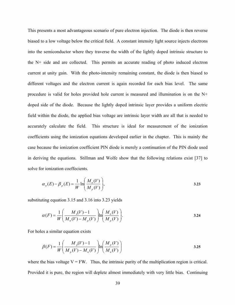
This presents a most advantageous scenario of pure electron injection. The diode is then reverse
biased to a low voltage below the critical field. A constant intensity light source injects electrons
into the semiconductor where they traverse the width of the lightly doped intrinsic structure to
the N+ side and are collected. This permits an accurate reading of photo induced electron
current at unity gain. With the photo-intensity remaining constant, the diode is then biased to
different voltages and the electron current is again recorded for each bias level. The same
procedure is valid for holes provided hole current is measured and illumination is on the N+
doped side of the diode. Because the lightly doped intrinsic layer provides a uniform electric
field within the diode, the applied bias voltage are intrinsic layer width are all that is needed to
accurately calculate the field. This structure is ideal for measurement of the ionization
coefficients using the ionization equations developed earlier in the chapter. This is mainly the
case because the ionization coefficient PIN diode is merely a continuation of the PIN diode used
in deriving the equations. Stillman and Wolfe show that the following relations exist [37] to
solve for ionization coeffecients.
⎟⎟⎠
⎞⎜⎜⎝
⎛=−
)()(
ln1)()(VMVM
WEE
p
npn βα , 3.23
substituting equation 3.15 and 3.16 into 3.23 yields
⎟⎟⎠
⎞⎜⎜⎝
⎛⎟⎟⎠
⎞⎜⎜⎝
⎛
−−
=)()(
ln)()(
1)(1)(VMVM
VMVMVM
WF
p
n
pn
nα . 3.24
For holes a similar equation exists
⎟⎟⎠
⎞⎜⎜⎝
⎛⎟⎟⎠
⎞⎜⎜⎝
⎛
−
−=
)()(
ln)()(
1)(1)(VMVM
VMVMVM
WF
n
p
np
pβ 3.25
where the bias voltage V = FW. Thus, the intrinsic purity of the multiplication region is critical.
Provided it is pure, the region will deplete almost immediately with very little bias. Continuing
39

improvements in epitaxial growth purity make this ideality more of a reality. In this fashion,
ionization coefficients at different fields can be accurately recorded.
3.6 Impact-Ionization Response Time
The manner in which different carriers behave during impact ionization has a significant
effect on the over all speed of a device. The ionization ratio between electrons and holes is K,
where K=β/α. Semiconductors with a small K experience shorter carrier transit time within a
high field region because impact ionization events are dominated by a particular carrier. This is
best illustrated by a best and worst case scenario. For a best case scenario, consider a
semiconductor where only electrons ionize.
If only electrons initiate impact ionization, β=0 and K = 0. Impact ionization events
caused by an electron entering the multiplication region of this semiconductor are illustrated in
figure 3.6 a). Because holes never create impact ionization events of their own, it becomes
evident that the time required for the ionization event to pass through the multiplication region is
the time required for an electron and hole to traverse the region. Because the transit time across
the region is independent of the number of ionization events that take place, there is no gain-
bandwidth limitation due to ionization. Contrast this to the semiconductor seen in figure 3.6 b)
where α = β or K = 1. In such a case, each electron creates secondary electron hole pairs which
in turn create secondary electron hole pairs of their own and the ionization process is self
sustaining.
In reality, semiconductors have ionization coefficients that lie between the two examples
given above. Since ionization events triggered purely by a single carrier have no effect on gain-
bandwidth, there must be some extent to which a semiconductor with a significant difference
40

between electron and hole ionization coefficients can produce a moderate gain with little or no
significant effect on gain-bandwidth. This is indeed the case [4]. Emmons shows that provided
that the DC multiplication gain M < α/β, such multiplication does not effect the gain-bandwidth
of the device. When M > α/β, gain bandwidth follows equation 3.26 below
. 3.26 [ 2/121
20
20 1/)( τωω MMM += ]
Figure 3.6: These figures illustrate the time difference for a small ionization event to completely traverse the depletion region where a) only electrons cause ionization events and b) where electrons and holes are equally likely to cause ionization events.
41

In this equation τ1 corresponds to the effective transit time and is approximated by τ1 =
N(β/α)τ, where N is a number that varies slowly from 1/3 to 2 as β/α varies from 1 to 10-3. τ is the
transit time equal to W/vs where W is the width of the avalanche gain region and vs is the
saturation velocity. Plotting this equation for various gains and ratios of β/α against the
normalized 3 dB cutoff gives the plot shown in figure 3.7. Figure 3.7 uses equation 3.26 to
further illustrate the effect that a large or small K have on bandwidth. Requirements for a high-
speed, responsive avalanche device include a large disparity between electron and hole
ionization coefficients, a small multiplication region, and high carrier saturation drift velocity.
Figure 3.7: Avalanche multiplication 3dB frequency response limits due to differences in ionization coefficients of electron and holes [4].
42

3.7 Multiplication Noise
Just as a low ionization ratio improves the overall gain bandwidth of impact ionization
based devices, it also decreases the noise generated by such events. When both electrons and
holes undergo impact ionization, they create the regenerative feedback mechanism illustrated in
figure 3.6 b). Lower feedback is desirable as it limits the number of carriers that can create the
random, non-deterministic noise generated by impact ionization known as excess noise.
Because of its random, non-deterministic nature, some carriers undergo few impact
ionization events while passing through a multiplication region while others undergo far more
than the average. This wide distribution of possible gains from individual carriers causes the
square of the average gain <M>2 to be somewhat smaller than the mean square gain <M2>. This
is significant as Webb and McIntyre [5] point out that the excess noise factor F can be defined as
2
2
><><
=MMF . 3.27
Thus F is a ratio of the actual noise caused by the random and haphazard nature of impact
ionization to a deterministic process where carriers undergo equal ionizations. More light is shed
on possible methods to minimize excess noise by examining the following equations. For
electron injection, excess noise factor is
) 3.28 1)(/12( effeeeffe kMMkF −−+=
and for hole injection
, 3.29 )1)(/12( '' −−−= effhheffh kMMkF
where Me and Mh are respective electron and hole gain and
∫∫=≈−
−=
2
1
2
1
1 222
2
22
1
x
x
x
xeff dxMdxMk
kkk
k αβ 3.30
43

and
2
22
1
22
1 2
1
2
1
2
1
2
1
⎟⎟
⎠
⎞
⎜⎜
⎝
⎛=≈=
∫∫
∫∫x
x
x
x
x
x
x
xeffeff
MdxMdx
dxMdxM
kk
kk
k
αβ
αβ
. 3.31
In this last equation, the <M2>/<M>2 term that defines excess noise factor can be readily seen in
k2/k1. Notice from equations 3.28 and 3.29 that as keff or k’eff approach a value of one, Fe and Fh
approach Me and Mh. In such a case, the excess noise factor would be equal to the device gain.
In like manner, as keff and k’eff approach zero the excess noise factor approaches a value of (2-
1/Me,h). Thus excess noise caused by impact ionization is most reduced by semiconductor
devices with a small K = β/α value.
Figure 3.8: Excess noise factor as a function of gain for multiplication regions with varying ratios of ionization coefficients [5].
44

Reduction of excess noise is mostly a materials game. The excess noise factor, Fe is
plotted by McIntyre in figure 3.8. Here again as noted in the previous section, operating at a low
gain is most advantageous. Notice that for materials such as silicon, gains of 10 can be
theoretically achieved without introducing significant excess noise such that silicon with a K =
(0.02 – 0.002) can operate at low gains as though k = 0. Engineering the multiplication region
can also help reduce excess noise factor. Advances in epitaxial growth techniques have helped
create Impact-Ionization Engineered (I2E) APDs. These devices reduce excess noise factor by
making the impact ionization events more deterministic and by reducing hole ionization
probability. The multiplication region of this diode is seen in figure 3.9 [6]. Notice the
reduction in bandgap across the 100 nm multiplication region.
Figure 3.9: The multiplication region of an I2E avalanche photodiode. By engineering the bandgap across the multiplication, excess noise is deterministically inhibited as secondary holes drift through progressively larger bandgap materials [6].
45

As electron begin to traverse the multiplication region from left to right, ionization energies in
the wide bandgap semiconductor coupled with its short width inhibit impact ionization. As
electrons continue to drift, they enter materials with lower bandgaps. This transition means that
the electrons suddenly have ample energy to ionize secondary carriers. The primary and
secondary electrons continue to drift through materials of progressively smaller bandgap while
secondary holes drift through materials of progressively larger bandgap. Thus the progressive
change in bandgap, coupled with the short ionization region fosters electron initiated
multiplication while inhibiting hole initiate multiplication. This creates a more single carrier
ionization effect and significantly reduces excess noise. An I2E APD with a “centered well”
Al0.2 Ga0.8 As multiplication region exhibited and excess noise factor equivalent to a
semiconductor with K = 0.1 while operated at gains below 20 [6].
While silicon has a most excellent impact ionization ratio (K = 0.02 - 0.002) a recently
explored alloy appears to be even better. During ionization Hg0.7 Cd0.3 Te exhibits pure electron
ionization without generating holes. As stated earlier, no semiconductor exists with impact
ionization ratios for K = 0. While this is true of all impact-ionization based mechanisms, Hg0.7
Cd0.3 Te is different because electrons ionize via ballistic ionization. Unlike impact ionization,
ballistic ionization takes place in Hg0.7 Cd0.3 Te because the ionization energy of electrons is
equal to the bandgap and the ionization energy of hole is twice the bandgap. This disparity
coupled with uncommonly light electrons and heavy holes allows electron to generate secondary
electrons during multiplication without ionizing holes [38]. Unlike impact-ionization, ballistic
ionization is a deterministic, history dependant, non random process. In consequence of this
condition, the square of the average gain <M>2 should be equal or very close to equal to the
mean square gain <M2> [39]. This appears to be the case as a device using ballistic ionization
46

called the Electron Avalanche Photodiode (EAPD) has been developed which exhibits a gain
bandwidth greater than 2 GHz and an excess noise factor of 1.25 without dependency on gain.
As pointed out in equation 3.18, pure electron ionization creates a region which never breaks
down. This is turns out to be the reported situation [40]. This device does not appear to utilize
so called “tunnel-impact ionization” which is another ionization process predicted in low
bandgap materials [30]. While this device has only been verified experimentally, discovery of
this alloy is exciting.
Studies have shown silicon to create the least excess noise during impact ionization. This
is primarily due to the large disparity in the ionization coefficients of electrons and holes [34].
This disparity quenches a natural feedback mechanism found in III-V semiconductors. In III-V
semiconductors ionization coefficients for electrons and holes are typically about the same. This
low noise property makes silicon the best semiconductor for impact ionization gain. Since the
SIM can accept current from a photodiode of any material, silicon is the viable and robust choice
for impact ionization despite its inability to detect light past wavelengths of 1 um and lattice
match with III-V semiconductors.
3.8 Conclusion
Current benefits supplied to society via impact ionization devices, is merit alone for the
extensive quantities study that has been conducted semiconductor multiplication gain. Yet the
equations, theories, and phenomena described in this chapter are not dead and things of the past.
They are guide posts that point the way to improvements in current devices and development of
new ones.
47

48

4 FUNDAMENTALS OF THE SIM
4.1 Introduction
The Solid-state Impact-ionization Multiplier (SIM) is an electronic device capable of
producing impact ionization based current gain for a signal from an arbitrary current source.
Other devices such as avalanche photodiodes (APDs) [41] and IMPact ionization Avalanche
Transit-Time (IMPATT) diodes [42] also utilize impact ionization gain. The difference between
the SIM and these devices is that current sources for APDs reside within the depletion region of
the device itself. IMPATT diodes rely on an external voltage source to induce avalanche gain in
the depletion region of the device. Consequently, a current source cannot be “wired up” to either
of these devices and exhibit a steady-state current gain over unity. However, the SIM
accomplishes this very purpose. Impact ionization based gain is attractive because it provides a
low noise amplification solution to systems detecting small current signals. This is illustrated by
the continued use and development of APDs for the detection of low light signals. APDs
provide additional gain to a photocurrent generated within their depletion regions while
operating below the noise floor of subsequent transistor based amplifiers (transimpedance
amplifiers) used to convert current into readable voltage levels. Thus low light levels are
detected that would be indistinguishable without the additional gain provided by the APD. The
SIM operates in a similar manner. A current source feeds signal into the SIM where it is
amplified and then fed into a transimpedance amplifier (TIA) for voltage readout. Potential
49

current sources compatible with the SIM include photodiodes made from any semiconductor
(and thus sensitive to a large selection of light wavelengths) and charge collectors.
Initial or first generation SIM designs were fabricated on silicon substrates and then
measured [43], [44], [45] to confirm that impact-ionization based gain is present in these devices.
Photodiodes constructed from silicon and indium-gallium-arsenide (InGaAs) were connected to
devices under test and exhibited significant current gain from photocurrent generated by visible
and near infrared (λ = 1300 nm) light sources. Work done previously by Hong-Wei Lee [3]
focused primarily on DC gain in first generation devices from a DC current injection source.
Most applications envisioned for the SIM involve current pulse detection. Thus it was of interest
to evaluate the frequency response of the SIM. This chapter investigates the parameters
contributing to SIM frequency response. This naturally emphasizes the resistive and capacitive
elements that establish the fundamental speed limitations for these first generation devices. This
chapter will cover the theoretical SIM operation and also model calculated and measured
frequency responses of first generation SIM devices.
4.2 Current and Voltage (IV) Characteristics of SIMs
An accurate explanation of the frequency response of the SIM best begins with a precise
description of current versus voltage characteristics, from which a circuit model is developed.
Throughout the progression of the first generation devices, current versus voltage plots were
presented in several different papers [43],[44],[45] these papers reported general findings and
theories that pertained to the location of impact-ionization within the SIM and the factors that
contributed to gain in the SIM. In a more recent work [46], which is the basis for this chapter, a
more thorough description is given. In harmony with that paper, this section discusses carrier
50

movement, carrier injection mechanisms at the device’s metal semiconductor barrier, and biases
at critical nodes of the device. Figure 4.1 illustrates the structure of first generation SIMs. This
represents a “vertical SIM” in which the high fields capable of impact-ionization are positioned
vertically between the N+ well and grounded P+ substrate. The fundamental idea behind the
SIM’s operation is that electrons are injected at the Schottky metal-semiconductor contact and
drawn toward the positively biased voltage (Vsim) node connected to an N+ doped region. This
N+ doped region is referred to as the electron collector. Electrons, injected at the input, move
through a high, horizontal field region toward the N+ doped collector and a vertical field
between the N+ doped collector and the P+ doped substrate. As electrons drift in this field, they
undergo impact ionization leading to the creation of electron-hole pairs. Newly created,
secondary electrons drift toward the low potential of the electron collector voltage, Vsim, while
newly created, secondary holes drift toward the grounded P+ substrate called the “hole sink.”
Drawing holes toward the “hole sink” instead of back toward the metal-semiconductor interface
allows the SIM to achieve current gain. Without a hole sink, secondary holes would find no
greater potential than the input node and drift toward it. In route to the input they would
recombine with newly injected electrons and eliminate any net gain produced by the device. For
operation with gain, the voltage at the metal semiconductor contact must be positive in relation
to the grounded substrate. With the substrate acting as the most favorable potential for holes,
secondary holes are drawn away from the metal semiconductor contact and towards the hole
sink.
The semiconductor doping and structure illustrated in figure 4.1 represents the first SIM
introduced. In reality, variations can be made to the device while maintaining the same
operation principle. For example, “Surface SIMs” employ hole sinks on the surface of a
51

semiconductor substrate through p-type doping, creating regions offset to either side of the N+
doped region (electron collector). These “Surface SIMs” have already been demonstrated [44].
All SIM devices were made using epitaxial silicon wafers with a low-doped P- layer on top of a
P+ substrate. Other possible variations include an N- doped epitaxial layer and a device
optimized for the injection of holes instead of electrons. A significant variation made to second
generation SIMs involves replacing the metal-semiconductor interface that comprises the input
with a heavily N+ doped ohmic contact. First generation devices only used a Schottky contact
input. The frequency response of the Schottky contact input is covered in this chapter while
other advantages to an ohmic contact input are reserved for subsequent chapters. Variation of
the above mentioned parameters requires further consideration of device geometry and
operational voltages to account for changes in doping, depletion layers, and electric fields.
However, for the sake of coherence, descriptions and measurements in this chapter consist of a
first generation vertical SIM design in silicon with a P- type epitaxial layer. Developing accurate
models for variations to this design should be straightforward and follow a similar structure.
Figure 4.2 shows a typical vertical SIM current versus voltage curve. Current is injected
into the device using a reversed biased photodiode illuminated with a light source. This
particular SIM has spacing d between the metal-semiconductor input and N+ collector of around
5 μm and is fabricated on a P- epitaxial layer of approximately 3 Ω-cm resistivity. The curve in
Figure 4.2 shows the current out of the electron collector (Isim) versus the voltage applied to this
node (Vsim). These DC measurements are done using an HP/Agilent 4156 Source-Measure Unit,
with the capability to bias and measure several voltage nodes simultaneously. This permits
simultaneous measurement and further evaluation of current flow through the photodiode, the
hole sink, and the electron collector.
52

Figure 4.1: First generation vertical SIM structure. This cross-sectional view of a device shows a P type epitaxial layer on a P+ substrate. The electron collector is the N+ doped region and the hole sink is the P+ doped substrate.
Figure 4.2: Graph showing Isim versus Vsim for a vertical device built using a P type epitaxial layer on a P+ substrate. An illuminated silicon photodiode served to inject current into the SIM.
53

Analysis of the Isim versus Vsim curve gives an idea of the carrier action within the SIM.
Figure 4.2 shows three distinct operation regions for the device – first a region where there is
very little current flowing through the electron collector, then a region in which the current
increases very rapidly, followed by a region in which the current increases further but at a more
gradual rate. Figure 4.3 illustrates these three distinct regions.
Figure 4.3: Representation of a model SIM current versus voltage curve with the 3 regions of interest labeled for discussion.
54

4.2.1 Region A
Figure 4.4 illustrates the SIM operation in region A. A constant negative voltage Vpd is
applied to a photodiode to keep it reverse biased. The hole sink of the SIM is grounded and a
positive voltage relative to ground reverse biases the collector to a voltage Vsim. Monitoring the
currents flowing in or out of these voltage nodes manifests a current flow into the node at Vpd
which is equal to the photocurrent being generated in the photodiode.
Current also flows out of the grounded hole sink, and virtually no current flows in or out
of the electron collector. These currents indicate that holes generated in the photodiode move
toward the negative Vpd node while electrons move toward the metal semiconductor input.
Holes from the P+ doped hole sink move toward the metal semiconductor interface and are
thermionically ejected under the metal-semiconductor barrier where they combine with electrons
in the metal as illustrated in figure 4.4 (b). The floating voltage Vms at the metal-semiconductor
interface adjusts to allow for enough hole current to flow under the barrier (by changing Θ) to
accommodate the incoming electron current flow from the photodiode. This means that Vms
must be negative in relation to ground and the Schottky contact at the metal-semiconductor
interface forward biased. With the SIM operating in region A, there is no appreciable current
flow into or out of the electron collector. Applying positive voltage Vsim, depletes the P- doped
semiconductor surrounding the N+ region and increases the electric field in these regions.
Because the extent of the depletion region is less than the spacing d between the electron
collector and metal-semiconductor contact, current injected at the metal-semiconductor contact
has no effect on current through the electron collector.
55
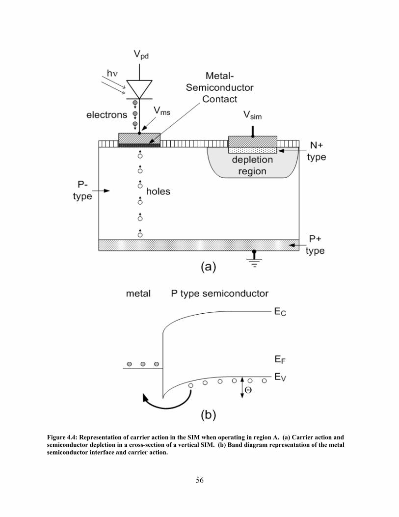
Figure 4.4: Representation of carrier action in the SIM when operating in region A. (a) Carrier action and semiconductor depletion in a cross-section of a vertical SIM. (b) Band diagram representation of the metal semiconductor interface and carrier action.
56

4.2.2 Region B
Figure 4.5 illustrates the operation of the SIM in region B. Vsim reverse biases the pn
junction which comprises the collector to a specific voltage Vdep. Monitoring of current flowing
through these nodes shows that current flows into the Vpd voltage node equal to the photocurrent
being generated in the photodiode, current flows out of the electron collector, and current now
flows into the hole sink.
These currents maintain the following relationship: Isim = current through the photodiode
+ current into the hole sink. These currents manifest the following carrier action: Holes
generated in the photodiode move toward the negative Vpd node while electrons move toward the
metal semiconductor interface and the floating voltage node Vms. Vsim has now reached the point
where the depletion region surrounding the electron collector has reached the metal-
semiconductor interface. Consequently, holes are no longer drawn up from the hole sink and
ejected under the metal semiconductor barrier. Rather (as illustrated in figure 4.5 (b)), electrons
are thermionically ejected over the barrier and into the depletion region. By lowering Θ, the
floating voltage Vms at the metal-semiconductor interface adjusts to allow for electron flow over
the barrier to equal the incoming electron current flow from the photodiode. This means that Vms
is now positive in relation to ground. The abrupt increase in current shown in figure 4.3
manifests the injection of current from the photodiode into the depletion region. While this
clearly indicates that a substantial amount of photocurrent is injected into the depletion region,
electron-hole recombination may still take place at the metal-semiconductor junction until the
depletion region moves across a substantial part of the metal-semiconductor contact.
57

Figure 4.5: Representation of carrier action in the SIM when operating in region B. (a) Carrier action and semiconductor depletion in a cross-section of a vertical SIM. (b) Band diagram representation of the metal semiconductor interface and carrier action.
58

Electrons ejected over the metal-semiconductor barrier drift in the depletion region
toward the electron collector. Finally, significant current flows toward this node. If the electric
field is high in the depleted semiconductor surrounding the electron collector, impact ionization
takes place creating electron hole pairs. Secondary electrons drift with injected electrons toward
the electron hole collector, while secondary holes drift toward the hole sink. The magnitude of
Isim is then equal to Ipd x G, where G is the current gain resulting from impact ionization. In like
fashion, magnitude of current flowing into the hole sink is equal to Ipd x (G-1).
4.2.3 Region C
Figure 4.6 illustrates SIM operation in region C. Vsim is reverse biased above the voltage
characteristic of region B (Vdep). Again the current flowing into the Vpd voltage node remains
constant and equal to the photocurrent generated in the photodiode, current flows out of the
electron collector, and current flows into the hole sink. The currents through the nodes maintain
the same relationship that was true in region B: Isim = current through the photodiode + current
into the hole sink. Carrier action in region C is similar to what happens in region B. Vsim has
now increased, however, increasing the strength of the electric field around the depletion region.
Electrons injected into this region experience more impact ionization events and the current Isim
increases according to Isim = Ipd x G. Holes created through impact ionization are still drawn to
the grounded hole sink.
Of note is the affect of increasing Vsim on the floating voltage Vms. Recall that the metal
semiconductor barrier adjusts to allow the current over the barrier to equal the current injected.
Because the amount of current injected into the SIM by the current source determines Vms, the
voltage between Vms and Vsim for a given input current remains constant and is given by Vdep.
Therefore, increasing Vsim above Vdep, merely causes Vms to rise according to Vms = Vsim – Vdep.
59

Vms varies with input currents, but for most conceivable applications this variation is relatively
small compared to Vsim – Vdep. The effect of “locking down” the voltage difference between Vsim
and Vms has several important implications for the SIM. First, the lateral extent of the depletion
region in the direction of the metal-semiconductor contact is constant d even as Vsim increases.
Figure 4.6: Representation of carrier action and semiconductor depletion in a cross-section of a vertical SIM when operated in region C.
60

Second, since the depletion region remains unchanged, the electric field profile also
remains the same. Any additional impact ionization must then be due to the increased electric
field between the N+ electron collector and the P+ substrate acting as a hole sink (vertical field).
The third effect of “voltage locking” is that increasing Vsim beyond Vdep has no effect on the
injection mechanism at the metal semiconductor and cannot raise or lower the barrier seen by
carriers as they enter the SIM.
4.3 SIM Circuit Model and RC Frequency Response Limits
The current versus voltage characteristics described in the previous section shed light on
several important factors that should be included in a circuit model for the SIM. These elements
include: 1) the Schottky diode between the metal-semiconductor contact and the P+ doped hole
sink, 2) a representation of the metal-semiconductor barrier that is dependent on the input current
and whether Vsim is greater than Vdep, and 3) a current gain element between the hole sink and
electron collector that can account for net impact ionization gain. In addition to these elements,
the circuit model should include capacitive and resistive terms present with p-n junctions and
metal to semiconductor contacts. Since SIMs have many characteristics in common with
avalanche photodiodes, a common model for these devices [5] has been adapted, neglecting for
now any temperature dependence for the device.
Figure 4.7 represents the circuit elements used to model the SIM. Included in this circuit
is a model for a photodiode being used as the current source connected to the SIM. The model
accounts for the connections between the three voltage nodes for the device. Between Vms and
the grounded hole sink, a diode is used to allow for current flow when Vms is negatively biased
compared to ground. In addition, a capacitor is added to represent the capacitance between the
61

metal-semiconductor interface and ground (including the contact pad necessary in real devices).
A series resistance and space charge term is also included. Between the metal-semiconductor
contact and electron collector (Vms and Vsim), the resistor Rbarrier is used to represent the
metal semiconductor barrier that is current dependent and infinitely large when Vsim < Vdep.
This is the barrier electrons see when injected into a depleted region between these nodes. The
resistance values for this barrier are developed in the following Section. A capacitor is also
included between the two nodes representing the capacitance between the metal-semiconductor
contact and electron collector. Between the electron collector and hole sink (Vsim and ground) a
dependent current source is used to represent the net impact ionization gain produced by the
device. Parallel to this current source, a diode represents the reversed biased p-n junction
between the electron collector and hole sink. Also parallel to the current source, a capacitor
represents the capacitance between electron collector and ground (including contact pads).
Finally a series and space charge resistance term is added between these two nodes. While this
model does not take into account effects like carrier transit time and impact ionization
multiplication delay times, it can provide a frequency response limit based on resistive and
capacitive elements for the device. As will be seen, these elements are a significant factor in
frequency response of current SIM designs.
Utilizing the circuit model in figure 4.7 to solve for the relationship between Isim and Ipd
at different operating frequencies ω, is fairly straightforward. However, the expressions for Isim
become quite muddled when including all of the elements found in the circuit model. Several
approximations can be made to derive a solution that is physically insightful and accurate in
most cases.
62

Figure 4.7: Circuit model for a SIM connected to a photodiode current source when Vsim is greater than the depletion voltage. I3 represents the impact ionization gain mechanism dependent current source.
The first approximations neglect the series and space charge resistances in the case of Rpd, R1s,sc,
and R3s,sc. In each of these cases, the series resistance is due to an ohmic metal-semiconductor
contact and so should be quite low. The space charge resistance comes from a relatively large
area contact over a thin depletion region and, so too, should be low. Typically series and space
charge resistances of this type are less than 50 ohms. Compared to other elements in the SIM,
these should have a very small effect on the overall response. The space charge term containing
63

the resistance R2s,sc is not to be neglected as it is quite significant (~10,000 ohms) due to the
large channel lengths and relatively short channel depths between the metal-semiconductor
contact and electron collector. The second approximation made is that the capacitive term C2
can be neglected compared to other capacitive terms and Rbarrier. Given that this represents the
capacitance between two nodes in a lateral direction on the surface of a wafer, this assumption
should be valid. Given these approximations, relationships for Isim and Ipd at given frequencies ω
are written in terms of the floating voltage Vms:
GRR
VIscsbarrier
mssim
,2+≈ , 4.1
and
[ ][ ]pdscsbarrierscsbarrier
mspd CCRRj
RRVI ++++
≈ 1,,
)2(12
ω . 4.2
Dividing (1) by (2) a relationship for Isim/Ipd is obtained.
⎥⎥⎦
⎤
⎢⎢⎣
⎡
+++≈
))(2(1 1, pdscsbarrierpd
sim
CCRRjG
II
ω. 4.3
The 3dB down frequency in which 2/1*=⎟
⎟⎠
⎞⎜⎜⎝
⎛⎟⎟⎠
⎞⎜⎜⎝
⎛
pd
sim
pd
sim
II
II is given by
))(2(21
2 1,
33
pdscsbarrier
dBdB CCRR
f++
≈=ππ
ω . 4.4
The simple relationship derived in (4.4) provides tremendous insight into the frequency response
limits for the SIM. Succinctly, the dominant terms consist of the barrier resistance at the metal
semiconductor interface and space charge resistance encountered by electrons between this
interface and the electron collector. Since a Schottky metal-semiconductor barrier height is input
current dependent, the barrier resistance or input resistance into the SIM and frequency response
64

manifest current dependencies as well. A derivation of the barrier resistance for this type of
interface is given in the next Section.
The accuracy of these assumptions that lead to the derivation of equation 4.4 was verified
by modeling the circuit in figure 4.7 in a Simulation Program with Integrated Circuit Emphasis
(SPICE). The 3 dB frequency responses match with less than 1% discrepancy for a large range
of component values. Because component values such as R1 and R3, were neglected or assumed
to be small (50 Ω) in the frequency response derivation, further simulations were needed to
determine the extent to which these values could be realistically ignored before noting a
substantial deviation from the calculated 3 dB frequency response. R1 and R3 typically represent
contact resistances and space charge resistance seen by carriers. Consequently, initial values for
R1 and R3 used in these simulations were small. However, because of possible space charge
effects that occur at high gains, resistance values ranged as high as 10 kΩ in the simulation.
Assuming realistic values for C1 and Cpd of 2 pf and 2 pf respectively, variations of R1 and R3
revealed a weighted two pole effect on frequency response. These poles are not evident in 4.4
due to simplifications intent on only revealing the most dominant pole, however, SPICE models
reveal their existence. R3 proved to be the dominant pole. Increases to R3 similar to those
mentioned in R1 caused simulations to deviate substantially from the derived frequency response
calculation. Increasing R3 to 1 kΩ caused 2% deviation and 55% at 5 kΩ. R1 proved the second
largest pole showing a 1% deviation on derived frequency response for 1k ohm and a 10%
deviation at 10 kΩ. Changing the values of C1 and Cpd can change the pole order dominance;
however, the capacitive values were specifically chosen to reflect a realistic scenario. The main
exception would be specifying the value of Cpd, which may exhibit substantial variation
depending on the type and speed of photodiode being used. Use of a sufficiently large
65

photodiode will reduce overall bandwidth by causing the photodiode itself, and not the SIM, with
a sufficiently large capacitance to become the dominant pole.
4.4 Metal-Semiconductor Barrier Resistance and Space Charge Resistance
Due to the important role the metal-semiconductor interface resistance plays in
determining the frequency response of the SIM, a derivation of the resistance can be made for a
vertical SIM with a Schottky contact on a P-type semiconductor. Rbarrier is based on the
thermionic emission of electrons over the barrier and is found by deriving a current versus
voltage relationship that is barrier height dependent. Figure 4.8 illustrates the energy barrier for
electrons between the metal-semiconductor contact and electron collector. This of course
assumes that the semiconductor layer between the two nodes is a constant doping and completely
depleted. As Vsim increases, the electron barrier height drops by ΔΘ allowing more electrons
over the barrier. The value for Rbarrier can be found by determining the relationship between
injected current and Vsim.
The current flowing between the metal-semiconductor contact and electron collector can
be described as
dkT
o IeII += ΔΘ / , 4.5
where k is Boltzmann’s constant and T the temperature [47]. The first term is related to
electrons ejected over the barrier and the second term, Id is due to current generation within the
depletion region (dark current). The Io term found in 4.5 is the current that would flow over the
barrier without any barrier lowering and corresponds toΘ . ΔΘ is the amount the barrier is
lowered by applying ΔV to the electron collector such that ΔΘ+Θ=Θbi , as shown in figure
4.8.
66

Figure 4.8: Energy band diagram showing the barrier for electrons injected from a metal contact into a SIM built on a P type epitaxial layer. After the P type semiconductor between the metal and N+ semiconductor is completely depleted, raising Vsim by ΔV will lower the barrier Θbi by ΔΘ as shown.
The derivative of the current versus this barrier lowering can be written as
kTII
ddI d )( −
=ΔΘ
. 4.6
To obtain resistance over this barrier, the derivative of I versus the voltage applied to the electron
collector is written as
simsim dV
dd
dIdV
dI ΘΔΘ−
= . 4.7
67

To obtain , a relationship between Θ and Vsim is made by examining the electric field in
the region between the metal-semiconductor contact and the electron collector when the
semiconductor between them is depleted. Figure 4.9 illustrates the electric field versus position.
simdVd /Θ
Figure 4.9: Electric field versus position in the depleted region between metal-semiconductor contact and electron collector. As Vsim increases, the slope of the electric field (-qNA/εs) remains constant and W decreases.
As indicated in figure 4.9, the area under the electric field curve between 0 and W is
equal to the height of the barrier Θ shown in figure 4.8 so that we can write
68

2
2WqNs
A
ε=Θ , 4.8
where q is the electron charge, NA the semiconductor doping level, and εs the permittivity in
silicon. W represents the distance into the semiconductor that the maximum barrier is positioned.
W will be the same as the depletion depth for an unbiased Schottky contact at the point where the
area between the nodes is first depleted (Vsim = Vdep). As Vsim increases further, W decreases in
length, but in most cases the change in the length of W is small because the barrier height
changes little to account for large changes in ejected current. Vsim is equal to the area under the
electric field between W and d, thus
( )2
2WdqNVs
Asim
−=
ε. 4.9
Using (4.8) and (4.9) the derivative for barrier height versus Vsim is
Wd
WdVd
sim −−
=Θ . 4.10
To account for changes in W with current, (4.5) and (4.8) can be used to derive the relationship
⎟⎟⎠
⎞⎜⎜⎝
⎛ −−Θ=Θ=
o
dbi
A
s
A
s
IIIkT
qNqNW ln22 εε . 4.11
Inserting (4.11) into (4.10) we can derive the derivative for barrier height versus Vsim that has a
current dependent term given by
⎟⎟⎟⎟⎟⎟⎟⎟
⎠
⎞
⎜⎜⎜⎜⎜⎜⎜⎜
⎝
⎛
−
⎟⎟⎠
⎞⎜⎜⎝
⎛ −−Θ
=Θ
1
ln2
1
o
dbi
A
s
sim
III
kTqN
ddVd
ε
. 4.12
69

Substituting the relationships from (4.6), (4.10) and (4.12) into (4.7) reveals
⎟⎟⎟⎟⎟⎟
⎠
⎞
⎜⎜⎜⎜⎜⎜
⎝
⎛
−
⎟⎟⎠
⎞⎜⎜⎝
⎛ −−Θ
−=⎟
⎠⎞
⎜⎝⎛ −
−=⎟⎟
⎠
⎞⎜⎜⎝
⎛=
−
1
ln2
1
o
dbi
A
sddsimbarrier
IIIkT
qN
dII
kTW
WdII
kTdV
dIRε
.
4.13
Space charge must also be considered in the SIM. Space charge resistance is caused by
the electric field reduction in a depletion region due to the presence of charge carriers. The field
reduction can be expressed as ΔEm = I d / (2ε0εsυA), where Em is the maximum value of the
electric field in the depletion region, d is the spacing between the metal semiconductor contact
and the electron collector, εs is the permittivity in silicon, υ the electron drift saturation velocity,
and A is the depletion region cross section area [45]. The equation indicates that with higher
current flowing inside the diode, field reduction will become larger. The field reduction can also
be realized as a corresponding voltage reduction equal to dΔEm. In this way the space-charge
effect is represented by an effective space-charge resistance
vAdR
ssc ε2
2
= . 4.14
The cross sectional area in the SIM device is estimated by the width of the depletion region in
the direction perpendicular to the path between the metal-semiconductor contact and the electron
collector, multiplied by the depth of the depletion region.
The magnitude of the two resistance terms (Rbarrier + Rsc) as a function of input current
into the SIM is verified by matching measured values with theoretical equations. Substitution of
actual device parameters into (4.13) and (4.14) yields a theoretical representation of Rbarrier + Rsc
versus input current as shown in figure 4.10. For this case, d = 4 um, P type doping equaled 3 x
70

1015, and the metal-semiconductor barrier equaled .45 eV [48] (nickel silicide on P type silicon).
A dark current (Id) of approximately 1 nA was used to represent the real device in (4.13). This
dark current term dominates the resistance curve at low currents. At high currents, space-charge
resistance dominates as Rbarrier drops below Rsc. Calculations for the space-charge resistance of
the device used in figure 4.10 yield a value of R2sc = 12 kΩ. Measured Rbarrier + Rsc for the
device with the same parameters are also shown in the figure to verify theory. Measurements
were made using an HP/Agilent 4156 with a grounded connection to the metal-semiconductor
contact while the contact to the electron collector is swept in voltage. The derivative of the
measured current versus swept voltage is then used to calculate the total resistance for a given
current. The calculated and measured values shown in figure 4.10 match very closely
confirming that thermionic barrier emission and space charge are the dominant resistance effects
in this particular SIM design (Schottky contact injection on P type semiconductor).
The implications of these resistance terms on the frequency response of this SIM design
can be shown by substituting (4.13) and (4.14) into (4.4), resulting in
⎥⎦
⎤⎢⎣
⎡+⎟⎟
⎠
⎞⎜⎜⎝
⎛+⎟
⎠⎞
⎜⎝⎛ −
−
≈
)(2
2
1
1
23
pdsd
dB
CCvA
dW
WdII
kTf
επ
. 4.15
The frequency response at low input currents is expected to exhibit a linear dependence on input
current. Given the large barrier resistances, frequency response is also limited as shown in the
following section.
71

Figure 4.10: Rbarrier + Rsc resistance versus input current between the metal-semiconductor and electron collector. The theoretical curve is calculated using (4.13) and (4.14) assuming a vertical SIM device made using a P type epitaxial layer, Schottky injection contact, and a spacing d equal to 4 microns. Measured values correspond to fabricated SIM devices with those parameters.
4.5 Frequency Response Measurement
The test setup shown in figure 4.11 measures the frequency response of first generation
SIM devices. In this setup, a sinusoidal signal drives an analog transmitter laser source (λ = 850
nm), allowing a single harmonic rather than multi-harmonic signal to be injected into the SIM
and used for frequency response evaluation. The laser passes through an attenuator before
72

reaching a photodiode. This provides a precise method to reduce electron photocurrent injected
into the SIM and facilitates the testing of device bandwidth at different but quantifiable current
injection levels. A Keithley 2400 Voltage-Measure Unit keeps the PIN photodiode reverse-
biased at all times and gives an accurate average measurement of the AC plus DC current leaving
the photodiode anode (Ipd). The vertical and horizontal fields necessary for impact ionization
and depletion are formed as a Keithley 2410 Voltage-Measure Unit reverse-biases the
semiconductor between the electron collector (Vsim) and hole collector (ground). Current is also
monitored using the Keithley 2410 as it flows either through the electron collector (Isim) or hole
sink (Isub). Electron current (-Isim) leaving the electron collector passes through a bias tee where
the AC and DC current components are separated. AC electron current is fed into a Femto
Current Amplifier acting as a transimpedance amplifier. This amplifier employs a virtual ground
on its input so that none of the AC signal is quenched or diverted through the DC leg of the bias
tee by having to pass through a high input impedance amplifier.
The current amplifier’s constant transimpedance gain of 5 x 10⁴ V/A provides a
substantial voltage signal that is averaged over several cycles to provide accurate measurement
and analysis on an oscilloscope. 3dB bandwidth is then determined as the frequency where the
voltage signal on the oscilloscope falls to 2/1 of its maximum value.
An HP/Agilent C-V Plotter 2480A, measured capacitance parameters necessary to
compare measured to predicted bandwidths. SIM device terminals were biased to voltages
conditions similar to those found in actual operation. For instance, depletion and pad
capacitances between the electron collector and hole sink were measured by biasing the junction
to potential identical to actual device performance before recording capacitance. Testing
73

included measurement of stray and additional capacitances caused by probes and substrate
electrodes.
Figure 4.11: Test setup used to measure the frequency response of SIM devices.
74

Figure 4.12: 3dB frequency response versus injected input current. Theoretical values were generated from equation 4.15 and measured values come from measurements on the same SIM device used to generate figure 4.11(P type semiconductor with Schottky injection).
Frequency response testing revealed a bandwidth dependant upon the amount of
photocurrent injected into the SIM as expected from (4.15). Using the setup illustrated in figure
4.11, several frequency response measurements were made on actual SIM devices at
progressively lower injected currents. The SIM was biased to a Vsim voltage greater than Vdep so
that the device was producing current gain. However, measured frequency responses were
independent of the gain produced in the SIM. This confirms that frequency response limitations
for this specific SIM design are due to RC effects and not impact ionization delay times. The
different values of injected current and actual device parameters including measured
75

capacitances (C1 + Cpd = 6.8 pF) were then used in the calculation frequency response using
(4.15). The total capacitance value also includes stray and additional capacitances from the test
probes used in the frequency response measurement. Actual and predicted values are matched in
figure 4.12. The specific SIM device used was the same one whose measured resistance values
are shown in figure 4.10 with dopings and geometry described in the previous sections. The
close match in both the frequency response magnitude and dependence versus input current
confirms the accuracy of the circuit model describing the SIM as well as the effects of the metal-
semiconductor contact barrier and space charge on device operation.
4.6 Conclusion
This chapter has explored the frequency response of first generation, vertical structure
SIM devices, and presented a theoretical model for response limits based on resistance and
capacitance parameters. Testing confirms the results presented from theoretical models. While
frequency response of these devices is significantly hampered by input current levels, the
developed models coupled with an understanding of carrier action within the device laid forth in
this chapter provide a clear path and solution to increasing the frequency response for redesigned
SIMs. Whether, such a solution will prove a detrimental to some of the SIMs other desirable
features will be addressed in subsequent chapters.
76
5 OHMIC CONTACT INJECTION NODE SECOND GENERATION SIMS
5.1 Introduction
In the first generation SIM, current from an external source was injected through a
Schottky contact as explained in Chapter 4. This chapter introduces a second generation SIM
design that utilizes a pn junction injection contact. This design makes the devices more
consistent to fabricate in several ways. Schottky contact characteristics can be highly dependent
on semiconductor surface and metal deposition conditions [49]. Using a pn junction injection
contact means that the points of injection and collection are both identical junctions.
Consequently, doping processes can be refined and optimized in tandem. Most importantly, the
Schottky contact SIM also suffers from frequency response limitations at low input currents due
to thermionic emission over the Schottky barrier. This chapter evaluates the frequency response
limits for the pn junction injection ohmic contact SIM or second generation SIM which was
investigated in the hopes of improving the SIM’s frequency response at low input currents. The
pn junction design while failing to improve frequency response in itself, provides an easily
fabricated device that can be optimized to reduce space charge resistance by altering the doping
profile of the device.
77

5.2 Ohmic Contact Electron Injection
Discovering the Schottky barrier input resistance in first generation SIMs provides
understanding on how such an obstacle can be overcome. Second generation SIMs seek to over
come this by employing an ohmic contact at the metal silicon interface. In this way, the work
functions of the heavily N+ doped semiconductor and metal fix the barrier height such that the
barrier into the semiconductor is pinned and cannot change with fluctuations in current as
electrons tunnel into the semiconductor (figure 5.1).
Figure 5.1: Illustration of an ohmic contact. This contact is used on the injection node of the second generation SIM to effectively inject electrons into the semiconductor.
The second generation SIM is fabricated on a p+ substrate with a p- epitaxial layer as
seen in figure 5.2a. Electrons are injected into the SIM through an n+ well.
In operation, a strong positive bias at the collector electrode reverse biases the junction between
the n+ well and the p doped regions creating a depletion region which grows toward the substrate
and input electrode.
78

(a)
0200400600800
0 5 10 15
Position (μm)
E-Fi
eld
(kV/
cm)
(b)
0200400600800
0 5Position (μm)
E-Fi
eld
(kV/
cm)
10
(c)
Figure 5.2: a) Cross section of the SIM showing the geometries and doping. b) Illustration of field profiles in the area of the horizontal cutline shown in figure 5.2a when VSIM is 50 volts and the injected current is 1 uA. c) Illustration of the field profiles for the vertical cutline in figure 5.2a under the same conditions as previously mentioned. Electric field lines were extracted from ATLAS simulations of the structure.
Electrons injected into the SIM enter the depletion region and drift toward high-field,
multiplication region near the positively biased electrode (figure 5.2b). Ionized electrons
produced in the multiplication region are collected by the positively biased N+ well while holes
are collected in the p+ substrate. Thus the second generation SIM design also prevents holes
79

from drifting toward the input electrode and recombining with incoming signal electron. This
collection of holes at the substrate occurs due to the favorable potential seen by the holes as they
near the hole sink (figure 5.2c).
5.3 Similarities and Differences Between the SIM, MOSFET and BJT
Replacing the earlier Schottky metal contact with an ohmic metal contact produces a
structure similar to a Bipolar Junction Transistor (BJT) or Metal Semiconductor Oxide Field
Effect Transistor (MOSFET) in that the injected electrons encounter an n-p-n doping profile as
they drift toward the collector electrode. However, several differences exist that make the SIM
unique from either the MOSFET or BJT. These differences include their mode or operation,
doping profiles, and device structure.
Under operational bias, the BJT and SIM have similar band profiles. In an NPN BJT,
electrons leave the emmiter by diffusing through a narrow base region into the collector. This
base region is heavily doped to reduce hole recombination in the emitter and quite narrow to
reduce the number of electrons lost due to recombination in the base. The high base ensures that
it is never significantly depleted from the large depletion region of the collector. While impact
ionization is achievable, though not desirable, in BJTs, no gain is possible because the base is so
narrow and confined that holes are not effectively drawn away before recombining with other
electrons. BJTs are not surface devices. Thus when examining the cross-section of a BJT, it is
evident that electrons typically move in a vertical fashion from the surface and into the bulk of
the semiconductor. In this way, electrons avoid any detrimental effects caused by the surface. In
the case of the SIM, region between input and collector which constitutes the base is large in
80

nature, lightly doped, and thus significantly depleted by the collector. Electrons also move
across the device surface fro the input to the collector.
The doping profile encountered in a MOSFET is identical to that used in the fabrication of
SIMs. Consequently, the wafers used to fabricate SIMs were originally designed for fabrication
of MOSFETs. The lightly doped epitaxial region in the MOSFET allows for quick inversion of
the channel between the source and drain while in the case of the SIM is allows formation of a
large, fairly uniform, high field region ideal for impact ionization. In an ideal sense, a MOSFET
could act as a SIM if it did not have a gate. The source could act as the input, the drain could act
as the collector and the substrate could act as the hole sink necessary to draw holes out of the
high field region. However, most discrete MOSFETs which have geometries large enough to
handle the high fields necessary for impact ionization only have three terminals in the packaging
because the substrate and source are tied together internally.
While impact ionization is possible in BJTs or MOSFETs, it is often called avalanche
breakdown rather than avalanche gain because the nature of impact ionization can damage the
device.
5.4 Second Generation Frequency Response
The behavior of the voltage on the input electrode is of critical importance in evaluating
the second generation device frequency response. Because of the high resistance exhibited by
external current sources such as photodiodes, the input electrode voltage cannot be externally
biased and is allowed to float in accordance to the level of current being injected into the device.
In the first generation Schottky based SIM, this floating voltage was determined using a model of
thermionic emission passing over a barrier.
81

In order to accurately model the behavior of the input electrode of second generation
SIMs, the quasi-Fermi level in the depletion region of the SIM must be considered. This is
because changes in current produce fluctuations in the quasi-Fermi level as charge is introduced
to the region. Consequently the voltage at the floating input node must be determined by
integration of the total field across the depletion region plus the integral of the charges
introduced into the depletion region after current injection [20]. This process, while rather
difficult to accomplish manually, is aided by the use of simulation and modeling tools from
ATLAS, the device simulation framework program by Silvaco.
By doing so it becomes readily evident that no improvement in frequency response is
manifest by introducing a pn junction input to the SIM. While the ohmic contact of the second
generation SIM removes the metal semiconductor barrier electrons see as they enter the
semiconductor, creation of the ohmic contact merely moved the barrier further into the
semiconductor. The voltage at the barrier floats in similar fashion to the barrier formed by a
metal-semiconductor junction. While the following derivation is different from the first
generation SIM, figure 5.3 helps to illustrate the similarity in the electron barrier problem
between the two devices by comparing the first and second generation SIM conduction bands.
Notice that in each case, electrons injected into the SIM face a potential barrier. In the case of
the second generation SIM, a voltage shift, ΔV, at the injection point into the depletion region is
related to the quasi Fermi energy shift (ΔEF) of the depletion region by
qEV F /Δ=Δ , 5.1
where q is electron charge. As the carrier density within the depletion region changes, a
corresponding voltage shift is produced due to the Fermi energy adjustment.
82

Figure 5.3: The difference in the conduction band structures of the a) Schottky contact SIM and b) the ohmic contact SIM. While the input resistance caused by the Schottky contact is eliminated, the built in voltage Θbi moves to the transition between the N+ doped region and the p- epitaxial region between the injection node and the collector.
83

The carrier density in a depletion region is dependent upon the current, I, through that region
by )/( qAIn ⋅⋅= ν , where A is the cross-sectional area of the depletion region and ν is the
carrier velocity through this region. The carrier density can also be defined as a function of the
Fermi level by
( )kTEENn FCc /)(exp −= or ( )CFc NnkTEE /ln⋅−=− , 5.2
where Nc is the density of states at the conduction band edge, k Boltzmann’s constant,
and T temperature.
Combining (5.2) with the relationship for carrier density yields
( )/(ln )ν⋅⋅⋅⋅+= qANIkTEE CcF . 5.3
Since injected current at the input naturally varies, there is a change in the Fermi energy. If the
current changes from I1 to I2, the change in the node voltage can be found by combining (5.1)
and (5.3) to obtain
. 5.4 ( 21 /ln)/( IIqkTV ⋅=Δ )
The shift in voltage at the injection node for a given input current is illustrated in figure 5.4 and
is directly related to the frequency response of the SIM.
This change in node voltage with input current results in an effective input resistance existing at
this node. This resistance is calculated by taking a derivative of equation 5.4
. 5.5 )/(/ qIkTdIdVR ==Δ
When combined with the depletion layer and current source capacitance, a charging time
constant, τ, is computed where
)/(qIkTCCR dd == Δτ . 5.6
84

Figure 5.4: Simulation of floating voltage at the input electrode for a range of input currents with 50 volts bias on the collector and the input being treated as a current source. Voltage values were extracted from ATLAS simulations of the structure shown in figure 5.2a.
Here Cd is the combined capacitance at the injection node. In the case of frequency response
evaluations Cd was dominated by the capacitance of the photodiode current source so Cd~20 pF.
The time constant τ represents the time delay for a change in the input current to change the
output current of the SIM. The large nature of this time constant limits the frequency response of
the second generation SIM to a frequency response similar to first generation SIMs. Thus when
RΔ is greater than the contact resistance it will have a detrimental effect on overall frequency
response. The results predicted by equation 5.6 for the ohmic contact based second generation
devices are similar to those of the first generation Schottky devices which also had a frequency
response that scaled by the inverse current. Table 5.1 compares these results. Notice that they are
similar in frequency limit with the pn junction device being slightly higher.
85

Table 5.1: Comparison of frequency limit of the Schottky contact SIM to that of the pn junction SIM.
3dB Frequency (kHz)
Current (μA) PN Junction
SIM Schottky
SIM
0.1 40 27
1.0 240 135
3.0 440 280
6.0 540 440
5.5 Fabrication and Testing
The second generation SIM was fabricated in silicon and modeled using ATLAS.
Selberherr’s model for impact ionization and the Shockley-Read-Hall recombination model were
implemented measure the ionization and carrier recombination events in regions of interest.
Fabrication began with silicon epitaxial wafers with an approximately 3 Ω-cm 10μm thick p-type
epitaxial layer and 0.01Ω-cm in the p-type substrate. A 30nm layer of silicon dioxide was
thermally grown on the silicon surface in a tube furnace. Wells of varying widths (30–360μm)
and spacing (3–9μm) that comprise the injection and collection contacts were then patterned with
photoresist on the oxide and sent for heavy phosphorus dose implants of 1e14 cm-2 at 30, 60 and
30 KeV. Wafers were then activated in a heatpulse 610 rapid thermal processor at 1050 C in a
forming gas environment for 30 seconds. Front and backside aluminum thermal evaporation
served to create a substrate contact and individual leads to devices. Wafers were then annealed in
86

a forming gas environment for 5 min at 450 C to produce low-resistance ohmic contacts to
heavily doped regions.
The current versus voltage relationship and current gain were measured in a similar
manner as first generation device in chapter 2 using a silicon photodiode (Perkin Elmer
VTP1012) as a current source and biased using an Agilent 4156 semiconductor parameter
analyzer.
Gain (M) was calculated in like manner as well where
input
darkoutput
III
M−
= . 5.7
Frequency response testing is similar to the testing of first genereation devices as
explained in Chapter 3. It consisted of wiring a reverse biased photodiode to the injection node
of the SIM. A laser emitting 870 nm light (Fiberlink XA-1000A-1) then illuminated the
photodiode, injecting electrons into the SIM. An Agilent 33250A waveform generator modulated
the laser. Source-meter units (Keithley 2400 and 2410) biased the SIM and photodiode while
monitoring all currents entering and exiting the SIM. The SIM’s output signal was connected
through a bias tee (Picosecond Pulse Labs 5530A) to a transimpedance amplifier (Femto HCA-
100M-50K-C) converting the ac output into a voltage signal. This signal was analyzed and
measured on an oscilloscope (Tektronix TDS 340A). The SIM was operated at an approximate
gain of 3 as obtained by equation 5.7 for the measurements shown in figure 5.5. The 3dB
frequencies versus various input currents are shown, and plotted along with a theoretical curve
based on equation 5.6. As the plot indicates the match of theory to experiment well. These results
are comparable and consistent to previous Schottky contact SIMs.
87

10
100
1000
10000
0.1 1 10Current (μA)
3dB
Freq
uenc
y (K
Hz)
Figure 5.5: Measured 3dB bandwidth for the fabricated SIM, represented by the diamond points, over a range of current levels. The theoretical response predicted by Eq. 5 is shown as a solid line, with 20 pF used for the node capacitance. A bias of approx. 40 volts was used.
5.6 Device Operation
5.6.1 IV Characteristics
Figure 5.6a shows IV curve measurements for different input currents along with ATLAS
simulations for equivalent devices. Notice that with the second generation SIM devices injected
electrons do not recombine with holes and the metal-semiconductor interface until the area
between the contacts is completely depleted. Rather a low bias on the collector is all that is
necessary to sufficiently deplete a path whereby injected electrons then drift to the collector
without undergoing recombination. This is easily observed in figure 5.6a by noticing that the
output current quickly assumes the sum of leakage current and injected current instead of
assuming only the leakage current until sudden spike in current indicate full depletion of the
device. With a low voltage applied to the output electrode, the electric field is too weak for
impact ionization to occur. As bias is increased, the depletion region approaches the n-well
88

beneath the injection point and electrons are injected into the depletion region where they drift
toward the positively biased output electrode without experiencing impact ionization. As
continued bias further increases the electric field, impact ionization begins to occur. Further bias
causes a sudden breakdown at the collector. This is indicated by a marked jump in the output
current at around 45 V for the device shown in figure 5.6a. Figure 5.6b shows the gain versus
voltage curve for the same device indicated in figure 5.6a.
It should be noted that the floating voltage at the input is not considered a direct function
of collector voltage. It is directly related to the current through the depletion region and thus
depends on the gain which is a function of collector voltage. Varying the spacing between the
input and output wells causes the devices to deplete at slightly different voltages but once
breakdown voltages are reached no noticeable effect on the gain or frequency response of the
device is seen.
5.6.2 Gain Control
Well designed silicon APDs and earlier SIMs [43],[46] exhibit gain curves that increase
more gradually with voltage. This is desirable because the gain is less susceptible to power
supply fluctuations and variations in temperature. The reason for the more abrupt breakdown in
this SIM can be explained by examining the electric field distribution shown in figure 5.2.
Figure 5.2a shows the device geometry while figure 5.2b and figure 5.2c show the electric field
extracted from device simulations along indicated cutlines in the horizontal and vertical
directions. The plots show that the electric field is high near the output electrode but quickly
drops off away from the output. Most of the impact ionization takes place in these high field
regions. Such a high field means that even small changes in field magnitude create large changes
in multiplication gain [50]. Consequently, small voltage changes on the SIM’s output node lead
89

to abrupt breakdown in the current versus voltage curves. Future SIM designs are designed in
such a manner to have more controllable gains.
1.00E-09
1.00E-08
1.00E-07
1.00E-06
1.00E-05
0 20 40Voltage (V)
Curr
ent (
A)
a)
0.1
1
10
100
0 10 20 30 40 50
Voltage (V)
Gai
n (M
)
b)
Figure 5.6: a) Collector current versus voltage for modeled and fabricated pn junction injection SIMs. The solid black and gray curves represent simulated injection currents of 50 nA and 500 nA respectively. These are plotted along side test results for 50 nA and 500 nA injection which are represented by diamond and triangle plots respectively. The leakage current curve for the fabricated devices is also shown and is represented by the x’s. The fabricated device had a width of 10 μm between the n-wells of the injection and output nodes. b) Gain (M) versus voltage curve for the same modeled and fabricated pn junction injection SIM devices from a).
90

This involves engineering the geometries in three dimensions so the electric field is
uniform and evenly distributed between electrodes. This is accomplished via alterations in
geometry and is the subject of the two subsequent chapters.
5.7 Space Charge Factor
It is important to remember that the main advantage of the pn junction SIM over the
Schottky contact SIM is its ease and consistency in fabrication. This change in architecture is
actually in attempt to resolve several issues that proved problematic in the first generation SIM
or judged necessary to implement the second generation SIM. One factor in particular which
needed to be addressed was gain saturation created by space charge resistance in first generation
devices.
Space charge governs the flow of current through regions of space where an electric field
is present. In the case of a semiconductor pn junction the built-in voltage of the semiconductor,
in combination with external bias create a space charge region through with current flows. At
high currents, the large numbers of carriers present within the region mask the influence of the
external field within the region and effectively lower the electric field. This reduction in field
due to high current density slows the drift of carriers across the region and reduces any gain
produced in multiplication areas. As noted earlier, this field reduction ΔE can be expressed as
ΔEm = I d / (2ε0εsυA), where Em is the maximum value of the electric field in the depletion region,
d is the spacing between the electron injection contact and the electron collector, εs is the
permittivity in silicon, υ the electron drift saturation velocity, and A is the depletion region cross
section area [45]. This field reduction can also be expressed as a resistance hence the term space
91

charge resistance
vAdR
ssc ε2
2
= . 5.8
Reduction of space charge resistance within the design parameters of the SIM is
primarily a game of reducing d and increasing A. The varying distances between input and
output nodes were sufficient to provide decent optimization of d, however, the cross sectional
area is quite small as evidenced by figure 5.7. Figure 5.8 shows the cross-sectional area of the
SIM. Increasing this cross-sectional area in a surface device like the SIM is more difficult that it
is in a planar device like an APD. In the latter case, carriers travel through the device in an
evenly spread manner. With a planar surface device, injected electrons spread evenly across the
wafer surface while maintaining a close proximity to the surface. Thus in the case of the SIM,
increasing the cross-sectional area is linear process where the electron collector is lengthened to
further spread the electrons across the surface of the SIM.
This is easily accomplished by making the electron collector contact longer and in turn
lengthening the injection contact in like manner. This permits the presence of higher currents,
via injection or multiplication, within the space charge region of the SIM before experiencing
gain saturation or decreased frequency response due to space charge resistance. While
fabrication of a Schottky electron injection contact long enough to compliment the increased
length of the electron collector would present a challenge of uniformity and yield, the sheet of
current flowing between input and output contacts may not be uniform due to preferential
silicidation of the Schottky metal into the silicon. Most importantly, a pn junction injection node
allows fabrication steps to be consolidated with formation of the collector pn junction. Thus
improvements in the doping process that manifest better uniformity and yield improve both
contacts.
92

Figure 5.7: Top view of the first generation SIM. With a 3 x 1.5 µm Schottky contact and a 10 x 10 µm Phosphorous doped well electron collection. The length between the Schottky contact and n+ region is varied between 3 and 9 µm for different device designs on the same substrate.
Figure 5.8: Illustration of the SIM showing the injection pn junction and collector pn junction. The collector pn junction is biased to produce a depletion region and the cross sectional area used to determine space charge resistance is illustrated.
93

5.8 Conclusion
The frequency response of second generation SIM is not significantly better than the first
generation Schottky contact SIM. Furthermore, the frequency response is limited in both cases
by a time delay required for carriers that enter the depletion region. For the second generation
SIM, the frequency response is limited by the resistive effects caused by shifts in the quasi-Fermi
level while the first generation SIM is limited by resistive effects caused by thermionic emission
over a barrier that changed height with changes in input current. These shifts are due to the
varying current levels through the depletion region and result in a kT/qI resistive limiting factor
in both devices. Considerations on how to overcome or reduce this resistive factor as well s how
to make gain curves more gradual and controllable are considered in subsequent chapters.
94

6 GAIN SHAPING VIA BURIED OXIDE
6.1 Introduction
A significant difference between the SIM and other impact-ionization based devices is its
three terminal design. All three terminals are necessary to facilitate impact ionization gain as
described in Chapter 3. However, three terminals immensely complicate the gradient of fields
within the SIM and consequently affect the preferred path of carriers.
Two terminal devices such as IMPATT diodes and APDs are built with one terminal on
the front of the wafer and the other on the substrate. Placement of these two terminals confines
carriers to the bulk of the semiconductor [51], [52]. Ring doping on the semiconductor surface
confines high fields and thus carriers away from the edges of the die. Because carriers can be
confined in this manner, carriers originate within the bulk, travel through the bulk, and avoid
contact with the semiconductor surface. Consequently, surface effects can be neglected in most
cases. A three terminal setup utilizing conventional VLSI fabrication requires that two terminals
reside on one surface. Thus carriers inevitably interact with the surface.
Surfaces often have a higher concentration of defects and impurities than within the bulk
wafer. Semiconductor surfaces behave like bulk semiconductor to the extent that they can be
passivated. This involves covalent bonding each surface atom with another atom or molecule
such that the electronic properties of the semiconductor are preserved. Fortunately for silicon,
silicon dioxide does just that. Other semiconductors are not so fortunate. III-V semiconductor
95

oxides do not passivate surfaces, but create defects that destroy electrical properties. Since
silicon dioxide (SiO2) can be thermally grown to satisfactorily passivate the silicon surface of the
SIM, the principle surface effect is one of electron field confinement.
6.2 Electron Confinement
The surface structure architecture of the SIM causes the majority of impact ionization to
occur near the semiconductor surface instead through the bulk of a semiconductor. Unlike an
APD, where signal carriers are optically introduced within the bulk of the wafer in the depletion
region, signal carriers in the SIM are introduced at the surface via the injection node and travel
horizontally to the output electrode. This horizontal current flow creates a challenge that
requires thoughtful device design to confine traveling electrons though the highest electric fields
within the SIM.
As injected electrons travel between the input electrode and collector, the fields between
them cause electrons to travel close to the semiconductor surface. Figure 6.1 shows an ATLAS
[Silvaco International, Santa Clara, California] simulation which illustrates the electric field
intensity within the device, while figure 6.2 illustrates the carrier path when electrons are
injected into the SIM. It is readily noticeable that injected electrons prefer to skim the surface of
the device between the oxide/semiconductor interface instead of travel through the bulk of the
device. While the high carrier concentration causes some carriers to diffuse vertically away from
the surface and into the highest field region of the collector, most of the carriers pass through a
lower field and experience little, if any, impact ionization. Thus, much of the input signal passes
through the SIM without being amplified.
96

Figure 6.6.1: Cross section of the ohmic contact SIM with Vsim=50V. Notice that the peak electric field resides at the corner of the N+ doping region roughly a distance D¬well from the SIM surface.
Figure 6.6.2: Cross section of the ohmic contact SIM with Vsim=85V and Iinjection=10μA. The current density represents injected electrons moving from right to left close to the surface of the SIM, and hole density primarily generated via impact-ionization being drawn from the left N+ doped well toward the P+ substrate.
97

This problem of poor gain efficiency can be remedied by a fabrication process that
introduces an insulator between the two surface nodes to shape the path of injected electrons.
This modification creates a new class of buried oxide devices and is referred to as a buried oxide
SIM.
6.3 Impact Ionization Efficiency
Electric field distribution and carrier path through the depletion region determine the
impact ionization efficiency of injected electrons. Where impact ionization is defined as follows
in
amp
nn
=η . 6.1
Where namp represents number of electrons that undergo impact ionization by passing through the
high electric field at the output node and nin the total number of injected electrons. The applied
bias at the output node creates the high electric fields within the SIM. As explained in Chapter 3
this bias creates a vertical field between the output electrode and the substrate and a horizontal
field between the injection point and the output. This combination of vertical and horizontal
fields creates a maximum electric field point located at the corner of the output pn junction as
illustrated in figure 6.1. Analyzing the carrier path and location of the maximum electric field,
it becomes apparent that the majority of the injected carriers do not pass through the optimal
multiplication region. Therefore only a small number of electrons are significantly multiplied. In
the case of low impact ionization efficiency, only a fraction of the total net injected signal
experiences high multiplication gain while the larger portion experiences little or no gain. This
causes an increased excess noise factor compared to a signal that is being uniformly amplified
[53], [41]. The electric field profiles shown in figures 6.1 and 6.2 were taken from simulation
98

with no leakage current. The absence of appreciable leakage current tends to increase the
magnitude of these fields. However, recently fabricated buried oxide SIMs typically have
leakage currents in the range of 200 pA to 1 nA. Thus the fields while not as strong still operate
in the same manner as shown in the figures.
To illustrate effects of low impact ionization efficiency on the gain versus voltage
relationship, consider Equation 3.11
∫ ∫∫ ⎥⎦
⎤⎢⎣
⎡−−−⎥
⎦
⎤⎢⎣
⎡−−
==L xL
n
nn
dxdxxxxdxxxJ
LJM
0 00
')'()'(exp)()()(exp
1)0()(
βαββα
6.2
which can be rewritten as
, dxdxxxdxxxML
x
LL
n ⎟⎠⎞⎜
⎝⎛ −−−⎟
⎠⎞⎜
⎝⎛ −−= ∫∫∫ ')()(exp)()(exp/1
00βαββα
6.3
where α and β are the electron and hole ionization coefficients. When all injected electrons
contribute to the multiplication gain (Mn) then the output current, Iout, is defined as
, 6.4 ninout MII =
where Mn represents the average gain experienced by all electrons where Iin is the input current.
In the case where a fraction of the injected electrons experience multiplication by entering the
high field region
)1( ηη −+= inninout IMII . 6.5
Since α and β are dependant upon the magnitude of the electric field in which the carriers
are found by
⎟⎟⎠
⎞⎜⎜⎝
⎛−=
)(exp 2
1 xEaaα , 6.6
99

and
⎟⎟⎠
⎞⎜⎜⎝
⎛−=
)(exp 2
1 xEbbβ . 6.7
Here, a1, a2 and b1, b2 are constants which depend upon the range of the electric field’s
magnitude [54].
Using Equations 6.3 - 6.7, relative gains for 100% efficiency and 1% efficiency are
plotted in figure 6.3 and show the importance of high impact ionization efficiency. Observe that
dM/dV, the rate of change of the gain with respect to voltage, varies with efficiency. For the 1%
efficiency case, this rate is much larger for a given voltage. Lower dM/dV is generally preferable
because it gives greater flexibility to addressing factors that cause the gain to drift such as power
supply voltage fluctuations and gain shifting due to temperature fluctuation. However, in the
case of Geiger mode impact ionization devices a large dM/dV is preferred because it increases
the probability of a photon successfully initiating an ionization event. It also improves
quenching time by reducing the voltage reduction necessary to terminate the ionization event
[55]. For a SPAD this large dM/dV is desired and necessary. However, a large SIM dM/dV
means that only a small percentage of the injected electrons contribute to the total device gain
while most contribute little or no gain. It is for this reason that poor gain efficiency requires a
large dM/dV to achieve appreciable gains.
The fraction of electrons that enter the high multiplication field is based upon the vertical
penetration depth of the high field region with respect to the device surface. The only electrons
which significantly contribute to gain are those which vertically diffuse away from the surface to
a depth where high multiplication fields exist. The vertical distance into the device that the
carriers are able to diffuse is governed by
100

dxndD
dtnd
nxΔ
−=Δ
, 6.8
where Δn is the change in carrier concentration and Dn is the diffusion coefficient for the
material [56].
Figure 6.6.3: Theoretical gain vs. voltage (M vs. V) plot as produced by equation 6.5 showing how the gain curves rise very abruptly with a low electron injection efficiency. It compares the theoretical cases of 1% efficiency for electron injection into the high field region and 100% efficiency.
Thus the concentration of carriers that diffuse into the bulk is proportional to the concentration
gradient at point x and inversely proportional to the distance [57]. The number of carriers that
diffuse into the bulk a distance d changes dramatically for a constant diffusion time.
101
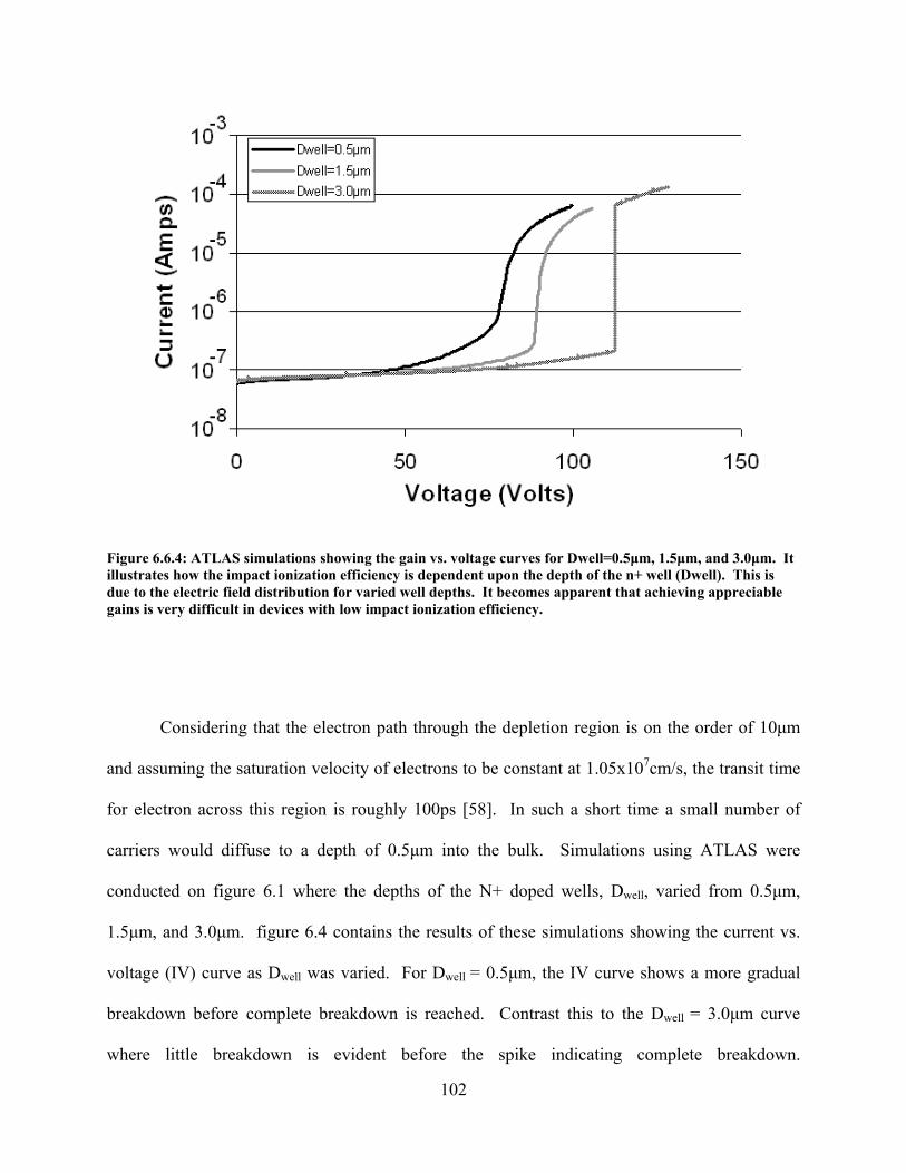
Figure 6.6.4: ATLAS simulations showing the gain vs. voltage curves for Dwell=0.5μm, 1.5μm, and 3.0μm. It illustrates how the impact ionization efficiency is dependent upon the depth of the n+ well (Dwell). This is due to the electric field distribution for varied well depths. It becomes apparent that achieving appreciable gains is very difficult in devices with low impact ionization efficiency.
Considering that the electron path through the depletion region is on the order of 10μm
and assuming the saturation velocity of electrons to be constant at 1.05x107cm/s, the transit time
for electron across this region is roughly 100ps [58]. In such a short time a small number of
carriers would diffuse to a depth of 0.5μm into the bulk. Simulations using ATLAS were
conducted on figure 6.1 where the depths of the N+ doped wells, Dwell, varied from 0.5μm,
1.5μm, and 3.0μm. figure 6.4 contains the results of these simulations showing the current vs.
voltage (IV) curve as Dwell was varied. For Dwell = 0.5μm, the IV curve shows a more gradual
breakdown before complete breakdown is reached. Contrast this to the Dwell = 3.0μm curve
where little breakdown is evident before the spike indicating complete breakdown.
102
Theoretically, improving impact ionization efficiency could be remedied by shallow well doping
on the input and output electrodes. However, this is fairly difficult as high voltages could cause
the shallow wells to completely deplete. The answer lies in a buried oxide layer between the
wells.
6.4 Benefits of Buried Oxide for Increased Ionization Efficiency
The constraints necessary to improve gain efficiency in the SIM led to the
implementation of an oxide layer placed between the wells and buried into the bulk to a depth
equal to or greater than the depth of the N+ wells. Figure 6.5 illustrates this structure with
applied bias but not injected current and figure 6.6 shows the structure in gain mode with
injected current. This oxide layer optimizes ionization efficiency by effectively shaping the path
of injected carriers in a way that guides the majority into the maximum field region. Comparing
figures 6.1 and 6.5 shows that introduction of the oxide does not affect the electric field. The
maximum electric field is at the same point as would be expected regardless of the depth of the
oxide dox. While the carriers still tend to travel along the surface of the silicon and while there is
still some diffusion into the bulk of the device, the oxide guides the vast majority of injected
carriers into the high field region.
Figure 6.7 illustrates the improvement in gain vs. voltage from data obtained from
ATLAS simulations on SIMs with and without the buried oxide layer. The gain behavior
between the oxide and no oxide case are significant. More importantly, the amount of voltage
required to produce a gain of 10 was roughly 60 V for buried oxide and 93 V for no oxide.
103

Figure 6.5: Buried oxide SIM showing the total current density for Vsim=50V and Iinjection =10μA where dox=Dwell.
Figure 6.6: Sim cross section showing the total current density at Vsim=50V and Iinjection=10μA. It was necessary to decrease Vsim from that of the ohmic contact SIM shown in figure 5.2 to obtain current levels comparable to the low impact ionization efficiency configuration of ohmic contact SIM.
104

Without oxide a small number of carriers must undergo multiplication of 100 to 10,000 so that
the ratio between the total current out to the total current in is 10. Without oxide the gain of 10
occurs at fields that produce gains of 1000. Contrast this to the buried oxide device where a gain
of 10 occurs at fields that produce gains of perhaps 10.01.
Figure 6.7: Simulation results illustrating the gain vs. voltage for a comparison of the buried oxide SIM with the no oxide SIM. It illustrates how abruptly the gain curves change and demonstrates the benefit of the buried oxide in improving the impact ionization efficiency of the SIM.
The optimal ratio between the oxide depth and well depth is found through simulation.
Figure 6.8 shows simulations of dM/dV at M = 50 vs. oxide depths (dox) ranging from 0.0μm to
2.0μm with Dwell = 1μm. Thus dM/dV, at a realistic gain, exhibits significant dependence on
105

dox/Dwell. Intuitively, the ideal ratio between dox/Dwell is 1:1 because the oxide channels electrons
in the shortest path to the maximum electric field point. However, figure 6.8 also points out that
little efficiency is lost when dox is somewhat deeper than Dwell. This is because most carriers take
the shortest route to the lowest potential and the few carriers that do diffuse away are fairly
minimal and due to the carrier concentration gradient.
Figure 6.8: Results from ATLAS simulations extracting the derivative of gain (M) with respect to voltage (dM/dV) for various oxide depths (dox). In these simulations Dwell=1μm for the various oxide depths (dox=0.0μm-2.0μm). Using the output current-voltage curve, a gain (M) vs. voltage curve was produced for each oxide depth. Then selecting a gain of M=50 for all oxide depths, the derivative of gain (M) with respect to voltage (dM/dV) was taken.
106

6.5 Buried Oxide Device Fabrication
Actual buried oxide devices and standard devices were fabricated on silicon and
compared with simulation models. Fabrication of these buried oxide devices has evolved over
time to produce devices with better yield and higher gains. However, all these evolutions can be
lumped into two unique generations of fabrication. Figure 6.9 illustrates the fabrication process
for first generation buried oxide devices. These were fabricated on a p-type silicon epitaxial
wafer with an EPI layer of approximately 3 Ω-cm resistivity and 10μm thick with a substrate of
0.01 Ω-cm in resistivity. A 200-nm layer of LPCVD silicon nitride is then grown on the bare
wafer surface. While sputtered and PECVD silicon nitride do not inhibit oxide growth at high
temperatures, LPCVD silicon nitride works quite well during thermal oxidation as an oxide
growth mask provided the temperature and duration is not too long. This mask is then patterned
by removing portions of the silicon nitride by Reactive Ion Etching (RIE) so that only features of
varying widths (30–360μm) and spacing (3–9μm) remain. These features eventually become the
N-wells of the buried oxide SIM devices. The wafer is then immersed into a hot KOH solution
to etch the necessary pedestals. During the silicon pedestal etch, the silicon nitride acts as a
mask during the formation of pedestals 1.5 um in height. These pedestals create the necessary
electron confinement between the injection node and output node that is unique to the buried
oxide structure. The next step involves growing a thermal oxide over the wafer. At this time the
patterned silicon nitride, which acts as a mask in the pedestal growth, prevents the growth of
thermal oxide to the top of the pedestal during the oxidation step. This thermal oxide layer
creates the actual oxide between the wells necessary to passivate the silicon surface and confine
the electrons. During the oxidation phase, the silicon nitride inhibits oxide growth on the top of
the pedestal.
107

Figure 6.9: Buried Oxide SIM fabrication where a bare silicon EPI wafer is a) coated with LPCVD silicon nitride. b) The silicon nitride is patterned and dry etched to create a pedestal KOH etch mask and then c) KOH etched to create pedestals of desired height. d) With the silicon nitride KOH etch mask doubling as a thermal oxide growth inhibitor a thermal oxide is grown on the bare silicon. e) Following oxidation, the silicon nitride mask is removed with a quick RIE etch. f) A phosphorus doped spin on glass is then applied to the wafer and g) the field oxide acts as a diffusion barrier so that only the pedestals are etched during diffusion. h) Lastly, the spin on glass is removed and metal contacts are made to the doped pedestals.
Following oxidation, the silicon nitride mask is then removed with a light RIE etch to reveal a
bare silicon pedestal top ready for doping with the oxide on the sides of the pedestal and
surrounding field of the wafer acting as a doping mask. The lightness of this RIE etch is critical.
The RIE can significantly damage or over etch the silicon. Any damage that occurs during the
RIE etch must be repaired in the subsequent diffusion step. This damage is typically manifest by
generation centers which create large amounts of leakage current at high fields within the SIM.
Following the etch, the wafer is doped with Honeywell P-8545 phosphorus doped spin on glass.
108

Following diffusion, the glass is stripped off in buffered HF and front and backsides of the wafer
are metalized to create a substrate contact and individual leads to devices. The diffusion depth of
the phosphorus which forms the two N wells must be carefully controlled. If the doping reaches
below the depth of the pedestal, electrons in transit between the wells are no longer confined by
the oxide. This will effectively mitigate all effects of the oxide, so as mentioned previously, it is
important that the diffusion depth is less than the 1.5 um pedestal height. The front and back of
the wafer are then metalized appropriately.
After fabrication, a first generation buried oxide SIM device was cleaved perpendicular
to the N wells revealing the unique cross section of the buried oxide SIM. This cross section was
observed using a Scanning Electron Microscope (SEM). A SEM image of the cross section is
seen in figure 6.10.
A newer process to creating buried oxide SIMs has been created in a manner that
improves device yields and leakage currents. In the previously explained process, LPCVD
silicon nitride plays a pivotal role as a KOH etch mask and also as a thermal oxidation growth
inhibitor mask. However, LPCVD silicon nitride becomes difficult to remove after oxidation.
While it is true that silicon nitride can be wet etched in high temperature phosphoric acid, it can
no longer be cleanly removed in this manner after the stresses of high temperature thermal
oxidation. In consequence, RIE etching becomes the only option. As mentioned previously, the
power and ion bombardment involved in RIE etching is undesirable as it damages silicon and
creates high leakage currents. This is manifest in the relatively high leakage currents (300 nA)
of the first buried oxide SIMs. Furthermore, LPCVD silicon nitride deposition is an expensive,
extra process which would prove advantageous if eliminated.
109

Figure 6.10: Scanning Electron Microscope (SEM) cross section image showing the injection electrode side of the SIM and the formation of the oxide in the channel between the injection electrode and output electrode. Note that in this case dox extends below dwell.
In efforts to eliminate the LPCVD silicon nitride and ensuing RIE removal etches, newer
buried oxide SIMs use chemical mechanical polishing (CMP) to remove the oxide off the top of
pedestals. This method eliminates the need for silicon nitride and is a straightforward way to
expose the tops of pedestals for doping. Figure 6.11 illustrates the second generation buried
oxide SIM fabrication process. These were fabricated on a p-type silicon epitaxial wafer with an
EPI layer of approximately 3 Ω-cm resistivity and 10μm thick with a substrate of 0.01 Ω-cm in
resistivity. 100 nm of oxide is thermally grown on the wafer. The layer of oxide is patterned
110

with resist and the field oxide is etched in buffered HF so that features of varying widths (30–
360μm) and spacing (3–9μm) remain.
Figure 6.11: Fabrication of the second generation Buried Oxide SIM begins by growing a) thermal oxide to act as a KOH etch mask. b) The thermal oxide is then patterned to form the etch mask and c) KOH etched to form pedestals. d) The etch mask is then removed and e) thermal oxide is grown over the entire wafer. f) SU8 is then placed over the wafer to protect the field oxide during polishing and g) the oxide on the top of the pedestal is removed via Chemical Mechanical Polishing (CMP). After cleaning off the SU8, g) the exposed silicon pedestal tops are then doped with phosphorus spin on glass with the thermal oxide acting as a diffusion barrier. j) Lastly the spin on glass is removed and metal is patterned onto the doped pedestals.
111

These features mask of the tops of the pedestals as the wafer is etched in hot KOH to form
silicon pedestals of roughly 3 um. After etching a 500 nm thick layer of thermal oxide is grown
on the wafer. This passivates the surface, acts as a doping mask, and creates the buried oxide
feature between the N wells. SU-8 3005 is then spun on the wafers. The minimum thickness of
SU-8 3005 is about 3 um. This corresponds well to the top surface of the pedestals. The
conformal quality of SU-8 provides a flat field area with minimal beading on the tops of the
pedestals. Using CMP, the SU-8 beading on the pedestals tops is easily removed along with the
oxide layer on the pedestal top. After polishing, the SU-8 is removed and Honeywell P-8545
phosphorus doped spin on glass is applied and diffused into the wafer. Following diffusion, the
excess glass is removed in buffered HF and front and back sides of the wafer are metalized.
After metallization, wafers were annealed for 30 minutes at 450˚ C in a forming gas
environment. A detailed recipe of the second generation buried oxide SIM is found in Appendix
A.
6.6 Gain Measurements
DC measurements which compare the IV curve and dM/dV differences between buried
oxide SIMs and planar SIMs were conducted using a silicon photodiode (Perkin Elmer
VTP1012) as the current input source into the injection node of the SIM are illustrated in figure
6.12. It was illuminated by an 850 nm Fiberlink XA-1000A-1 laser. All nodes in the
measurement process were biased and monitored using an Agilent 4156 Semiconductor
Parameter Analyzer.
112

Figure 6.12: Testing setup used to verify gain differences between Ohmic Contact SIMs and Buried Oxide SIMs.
Figure 6.13 shows measurements for both planar and buried oxide devices and compares
them to ATLAS simulations of equivalent devices. The curves illustrate typical performance of
planar and buried oxide devices. At lower voltages, the electric fields produced are too small to
induce impact ionization. However, at higher applied voltages, current flowing between in nodes
triggers impact ionization. In the planar SIM devices, few electrons enter the maximum field
region [21]. Consequently, little if any gain is noticeable until high amplification of these few
electrons occurs as they pass through the maximum field. This dramatic change in field requires
a small change in voltage and results in a sudden jump in current. Conversely, buried oxide SIM
devices exhibit a more gradual increase in gain.
113

Figure 6.13: Current vs. voltage curves showing measured and simulated differences between breakdown voltage and gain. The Measured (No Oxide) data curves and simulation curves and Measured (Oxide) data and simulation curves were made from wafers identical in doping and similar in n-well doping profiles.
Figure 6.13 also shows the measured dark current levels for first and second generation
buried oxide SIMs and planar SIMs. Buried oxide devices show better signal to noise ratios and
second generation buried oxide SIMs exhibit much lower leakage currents. Most importantly,
second generation buried oxide devices exhibit stable currents, stable gain over time and do not
manifest any indication of device damage from normal operation.
6.7 A Note on Metallization
During evaporation, Aluminum will experience a eutectic reaction with silicon that is
caused by the heat lost during metal condensing on the wafer. While introducing a small
114

percentage of silicon into the aluminum can help reduce this problem, this is difficult because
during evaporation the vapor pressures of the two materials are so different that the aluminum
tends to evaporate first followed by the silicon [59]. Thus the silicon is often not located in the
film near the wafer interface where it is most needed to prevent eutectic spiking. Even with
silicon present in the aluminum, a small amount of spiking still occurs. Thus aluminum is not a
suitable material for contacting shallow doped wells. For the first buried oxide SIMs, a 100nm
thick nickel barrier metal contacts the doped silicon N wells and is followed by aluminum.
Nickel turns out to be a fairly poor barrier metal for aluminum. Aluminum is reactive enough
with nickel that at evaporation temperatures the aluminum will consume the nickel to form
aluminum rich NiAl3 [60]. If the amount of aluminum is very high, the aluminum consumes the
nickel and then consumes the silicon resulting in a spike through the doped portion of the silicon.
Furthermore, if the N well is very shallow, the nickel barrier metal may spike through the well
while forming a nickel silicide.
An excellent barrier metal option is combination of 5% titanium (Ti) 95% tungsten (W)
or platinum. Because of vapor pressure differences, an alloy of 5% Ti and 95 % W can only be
sputtered, however it is the barrier metal of choice for second generation buried oxide SIMs.
Proper annealing of the TiW alloy provides an excellent ohmic contact to N type silicon [61].
While 100% tungsten may work as an effective barrier, it does not adhere well to silicon dioxide
and thus requires additional lithography steps. Platinum, can be an excellent option. If arsenic is
used as a dopant instead of phosphorus as is the case for many shallow doping situations, then
platinum is probably the best option. During silicidation, platinum actually rejects incorporation
of arsenic dopant atoms. Consequently, the arsenic is pushed deeper into the silicon and piled up
to rest at the metallurgical interface. This “snow plow” effect on arsenic creates a very heavy
115

doping at the interface which further reduces the contact resistance of the platinum-silicide
contact [62].
Proper metallization for a given device structure has been one of the great challenges of
this research. Past generation SIMs designs produced low wafer yields with leakage currents
typically in the hundreds of nano-amps. Perfecting the metallization process has been a key
element in improving yields and reducing leakage currents.
6.8 The Importance of SU-8 in Planarization
The powerful, unique role of SU-8 in the planarization process involved in second
generation buried oxide SIMs is explained more fully in this brief section. In essence the SU-8
acts as a sacrificial layer that allows selective removal of the pedestal top oxide while completely
preserving the field oxide and oxide of the sides of the pedestals. Without the SU-8 acting as a
sacrificial layer, this is not possible.
The SU-8 plays a subtle role in the polishing. CMP is a process whereby wafers are
planarized. It is not desirable to planarize the pedestals doing so would cause the pedestals to be
rounded instead of flat on the top as they are polished off. SU-8 prevents this from happening.
To do this it is important that pedestals are purposely etched to the height near that of the
thickness of the SU-8 to be used. The SU-8 planarizes around the pedestals such that only the
top of the pedestals are above the planarized SU-8. In this way, the polisher quickly removes the
pedestal tops to the thickness of the SU-8 but slowly removes the SU-8 and silicon behind it
because the non-planar features have already been removed. It is also important to note that too
thick a layer of SU-8 will completely cover the pedestals and result in a very slow pedestal
removal process. This is because a chemical mechanical polisher is only effective at planarizing
116

a wafer. One the wafer is planar, it proves less effective at removing thick layers of planarized
substances. Consequently, if several microns separate the pedestals tops from the surface of the
SU-8, a long polish process must be endured as the polisher slowly removes the planrized SU-8
down to the pedestal top. In such a scenario, the SU-8 is likely to weaken and break away in
chunks causing poor overall results.
The effectiveness of incorporating the SU-8 sacrificial polish layer into the fabrication
process can be observed in such cases when the SU-8 fails to properly adhere. In such a case,
the SU-8 flakes away and the polisher quickly and completely removes the pedestals.
6.9 Layout Compensation when Considering the KOH Etch
When making buried oxide SIM pedestals via KOH etching, special care needs to be
taken in layout so that the final devices are the desired dimensions. Unlike most semiconductors,
silicon does not wet etch isotropically. It etches preferentially depending on the crystal plane
that is being etched. While this etching ratio varies depending on the etching solution, the ratio
between the (100) and (111) plane in a solution of potassium hydroxide (KOH) is roughly 100:1.
The slow etch rate of the (111) plane is often attributed its close proximity of silicon atoms. In
dry etchers, the (111) plane does not exhibit this resiliency and deep, high form factor features
can be made. Silicon wet etching in the end is the preferred method of fabrication because of the
low impact that it has on the electrical structure of silicon. Dry etching involves bombardment
of large ions at relatively high energies which can damage the lattice of the residual silicon. The
extent of this damage relates to the magnitude of RF power used to create the plasma. Wet
etching is confined to the silicon surface and relies on the electro-chemical properties of the
etchants to do the work. While wet etching silicon introduces more design constraints due to its
117

peculiar etching nature, the amount of damage done to the silicon lattice during dry etching,
makes wet etching a more advantageous route. These design constraints are discussed below.
With previous SIM devices the parameters that defined the electron channel length
between wells and the well width were defined roughly by the lithographic photomask
dimensions. While oxide etching and masking resist introduce some aberrations into these
dimensions, they are for the most part of negligible importance in SIM fabrication. With the
buried oxide design, much of the overall design is governed by the anisotropic silicon wet etch.
Because of the disparity between the (100) and (111) plane etch rates, significant etching in the
<111> direction is only noticeable in long etches. Since pedestal etches used to fabricate the
buried oxide SIM are relatively short any significant etching occurs in the on the (100) plane in
the <100> direction. This causes the (111) plane to form a beveled, unetched edge at a 54.75˚
angle to the (100) plane. Figure 6.14 illustrates how this effect reduces the electron channel
length (L). Notice as shown in Figure 6.14 a) that if
)75.54tan('2°
≤dL , 6.9
the new channel length formed by etching of the buried oxide SIM, L’, will effectively shrink to
the point of a blind cavity. This becomes a problem when the height of the doping depth within
the pedestals is equal to the pedestal height d’. In this case, the channel is completely destroyed
and doping within the pedestal effectively diffuses together. However, if the doping depth
within the pedestal is at a level d then the electron channel consists of the path around the blind
cavity point between the wells. Allowing creation of a flat channel between the pedestals
provides the desired electron confinement.
118

Figure 6.14: a) If the initial spacing between pedestals (L) is too small the etching will form a blind cavity of depth (d’) and no channel will exist between pedestals. b) The effective channel length (L’) of the etch changes from the initial distance (L) due to the anisotropy of the etch.
Solving the actual channel length L’ that is formed after etching the pedestals for the
buried oxide SIM is shown in figure 6.14 b). Notice in this case that the mask that protects the
119

silicon against wet etching must be spaced a distance L apart. A simple formula can be used to
calculate this and is seen below
°−=
75.54tan2' dLL . 6.10
Due to the nature of silicon KOH etching, the actual width of the pedestals is also
reduced by the etching. This can also be taken into consideration using the above equations.
Silicon KOH etching also constrains the structure of devices which can be built using this
method. A basic rule of thumb for silicon KOH etching is this, no matter the design of the
original etch mask, if etched long enough all silicon features will eventually look like four-sided
pyramids with a rectangular footprint. Consequently, rectangular pedestals are quite permissible
and work fairly well. While silicon KOH etching has many advantages over other forms of
etching, silicon’s anisotropic wet etching nature requires further layout considerations and limits
device geometries.
6.10 Conclusion
Easily maintained and controllable gain curves are desirable attributes in the SIM.
Buried oxide SIMs possess these attributes. Controllable gains in previous ohmic contact SIM
devices were unobtainable due to primary amplification occurring along the surface as opposed
to traditional impact ionization based devices that amplify vertically through the bulk of a
semiconductor. Amplification on the surface makes it difficult to achieve high impact ionization
efficiencies because of the path carrier take through the depletion region. Previously, most of the
injected current missed the highest multiplication gain region and passed through the SIM
without any amplification at all. Introduction on an oxide layer between injection and output
nodes shapes the path of injected electrons into the high multiplication field region of the SIM.
120

The ratio of oxide thickness to well depth (dox to Dwell) is an important consideration to allow for
maximum ionization efficiencies. Buried oxide devices show a significant improvement in
dM/dV when compared to the planar SIM design. At a DC gain of 18 the buried oxide SIM was
measured to have a dM/dV of 1.4 while the planar SIM had a measured dM/dV of 416. Thus
shaping the path of the electrons allows shaping of the voltage vs. gain profile of the SIM.
121

122

7 KEY ELEMENTS CRITIAL TO HIGH GAIN
7.1 Introduction
The development of larger well dimensions in the SIM was necessary to prevent
significant space charge resistance and gain saturation caused by higher injection currents and
multiplication gain. This increase in device geometry also saw the implementation of the pn
junction injection node instead of the Schottky injection node. These new devices also exhibited
gain which was quite poor and adoption of a buried oxide structure was necessary to improve
gains. However, this transition brought with it several phenomena between first generation
planar devices and buried oxide devices that were never explained but consistently evident.
These were the difference in breakdown voltage between second generation planar SIMs and
buried oxide SIMs and the sudden drop in gain between first generation SIMs and second
generation planar SIMs. Even more interesting, was the difference in junction breakdown
between rectangular devices and their circular counterparts. Just as rectangular buried oxide
devices broke down at higher voltages than planar diffused junction devices, circular pedestal
devices broke down at higher voltage then their rectangular buried oxide counterparts.
Investigation into breakdown voltage differences has led to the discovery of geometrical factors
which improve the breakdown voltage of the SIM and make fields more uniform to improve gain
efficiency.
123

7.2 Breakdown Voltage and Edge Effects
It is important to notice in figure 6.13, that planar SIMs experience break down at lower
voltages than buried oxide SIMs. This change in breakdown voltage is primarily due to the
change in geometries that are incorporated into the buried oxide structure. Planar diffused or
implanted junctions manifest a sharp curve at the edge of the well as the edge of the junction
reaches the oxide surface (Figure 7.1). The radius of curvature, rj, of this curve determines the
nature of the junction breakdown voltage. Devices with smaller radii of curvature produce
junctions which require a lower the bias voltage to achieve breakdown [7]. This curve profile
dependence is especially manifest in one-sided, abrupt junctions. Consequently the planar
doping profile of the SIM, which incorporates heavy phosphorus, n-type well diffused into the
lightly doped, p- epitaxial layer, creates a junction which breaks down prematurely.
Figure 7.1: Cross sectional planar diffusion or implantation side profile junction. A junction curvature rj is formed at the edges of the doped regions.
124

Two areas of interest which breakdown before the planar or flat portion of the junction are
regions of the junction which are spherical and cylindrical in nature. Those regions are
illustrated clearly in figure 7.2. These regions most likely get their name due to the type of
coordinate system which is necessary to solve for the fields in that region. Solving for the field
in these regions requires the use of Poisson’s equation which states
, 7.1 srrV ερ )()(2 −=∇
where the gradient of the voltage V(r) is equal to the electron charge density, ρ(r), times the
permittivity of silicon εs. For cylindrical and spherical junctions, equation 7.1 becomes
[ ]s
nn
rrErdrd
r ερ )()(1
= , 7.2
where n = 1 for a cylindrical junction and n = 2 for a spherical junction and ρ(r) for an abrupt
junction is –qNB for rj ≤ r ≤ rd. Solving for E(r) yields the following equation
∫ +=r
rn
nn
s jrCdrrr
rrE 1)(1)( ρ
ε . 7.3
Here, C1 is a constant of integration which must be set equal to Ψbi, the built-in potential of the
junction. Since breakdown voltage is of interest, the ionization equations are once again needed.
Multiplication of electrons as described in equation 3.13 is written as
∫ ∫⎥⎥⎦
⎤
⎢⎢⎣
⎡−−−
=2
1 1
')'()'((exp)(1
1r
r
r
r
n
drdrxxx
M
βαα
. 7.4
125

Figure 7.2: Illustration of an N-Well planar diffusion profile where the darkened area shows a) spherical regions and b) cylindrical regions.
126

Avalanche breakdown occurs at the voltage where the multiplication factor becomes infinite.
Rearranging the equation 7.4 the condition readily appears as
n
r
r
r
r Mdrdrxxx 11')'()'((exp)(1
2
1 1
−=⎥⎥⎦
⎤
⎢⎢⎣
⎡−−≡ ∫ ∫ βαα . 7.5
The equation for holes can be solved in a similar fashion. Using Chynoweth’s equation for
ionization coefficients, the electric field dependency of avalanche breakdown becomes
noticeable
( )(/exp, rEba −= )βα , 7.6
where proper selection of a and b provide accurate ionization values for electrons and holes.
Using equation 7.5 has a definition of device breakdown and equation 7.3 to compute the
fields, relation between junction curvature and breakdown voltage can be obtained. Such a
relationship is illustrated in figure 7.3. Examination of figure 7.3 shows a dependence in
breakdown voltage depending on junction geometry.
7.3 Breakdown Voltages in the SIM and Their Effect on Gain
This correlation between device geometry and device breakdown is of significant
importance in SIM design so that fields are engineered in a manner to provide optimal gain. The
SIM is not the first impact-ionization based device to suffer from field effects leading to
undesirable breakdown. Many APDs employ high field multiplication regions near the surface
of the wafer and use a combination of doping and guard rings to avoid premature breakdown. In
fact, many insights in possible SIM design improvement have been gained by examining APD
cross section structures similar to the cross section shown in figure 7.4.
127

Figure 7.3: Breakdown voltage Vb vs substrate impurity concentration, Nb, for plane, cylindrical, and spherical junctions for different radii of curvature [7].
Figure 7.4: 3D cross-section of an avalanche photodiode (APD). Electron hole pair generation occurs in the absorption region after which a current undergoes impact-ionization in the multiplication region and collected. Notice contoured doping of the collection well and floating guard ring to confine carrier to the high field region and prevent breakdown.
128

After examination of this cross-section it becomes evident that premature device
breakdown is not unique to the SIM. Rather premature breakdown is a factor that must be
reckoned with in high field devices. Some steps to reduce premature device breakdown
happened inadvertently in the buried oxide structure in effort to improve gain efficiency.
However, gain efficiency and device breakdown are linked such that improvement of one
naturally implies improvement of the other. How this actually happens is best illustrated by
figure 7.5. Figure 7.5a illustrates a typical planar diffused junction that is common to all SIM
devices before the buried oxide SIM. This device exhibits premature breakdown because of the
small radius of curvature, rj, at the edges of the junction. This junction also exhibits poor gain
efficiency as mentioned in the previous chapter because the highest electric field is at the corner
near the bottom of the junction and injected electrons skim across the surface missing the highest
field multiplication region. Improving the gain efficiency as seen from a cross-sectional view is
accomplished by introduction of a pedestal. Figure 7.5b illustrates how this confines surface
injected electrons into the high field multiplication regions as explained in Chapter 5. Device
breakdown is improved because a KOH pedestal increases the radius of curvature, rj. Using an
anisotropic dry etch provides pedestals with vertical side walls as shown in figure 7.5c. This
makes the diode completely planar in nature, because the cylindrical and spherical regions of the
diode are completely removed. Thus the device has the highest breakdown voltage. While
fringe fields still in reality exist, they remain confined to the oxide and air that surround the
pedestal.
Figure 7.5 illustrates an excellent method to improve fields to reduce premature
breakdown and improve gain efficiency. However, a strictly cross-sectional view of the SIM
will produce a satisfactory solution provided the SIM be of infinite length.
129

Figure 7.5: Illustrating different junction geometries to improve cross-sectional gain efficiency and reduce fields which create premature device breakdown.
130

Otherwise the corners of the rectangular well create problems of their own. This is easily
observed by examining the fields from above. The cross-sectional illustrations in figure7.5 show
that a pedestal device exhibits superior gain efficiency and device breakdown voltage, but
neglects such effects in a three dimensional device. Figure 7.6 illustrates the electric field
magnitudes looking down on the devices as calculated in a simulation using SILVACO. Notice
that the field is still highest on the corners of the collector. This high field region does not only
show the region which will cause premature device breakdown, but also shows the region of
highest multiplication gain. Thus while the rectangular pedestal buried oxide exhibits excellent
cross-sectional gain efficiency, the lateral gain efficiency as seen from above is quite poor.
Injected electrons from the input drift toward the collector to find the highest multiplication
region accessible to a small number of carriers.
Examining the fields from a cross-sectional and lateral viewpoint sheds light why
multiplication gains suffered significantly with the first pn junction electron injection device.
The collectors on first generation devices had a maximum length of roughly 10 microns. While
first generation collectors where square and had corners, their relatively short length of roughly
10 um meant that the corners comprised a substantially larger part of the junction than longer,
second generation, pn junction injecting devices. This also explains why shorter second
generation, pn junction injection devices often exhibited better gains than longer counterparts.
Elimination of sharp corners is most easily accomplished by creating a completely
circular, pedestal device. The pedestal confines cross-sectional fields and improves cross-
sectional gain efficiency while the circle addresses these same needs from a lateral viewpoint.
131

Figure 7.6: Electric field magnitude looking down at the SIM. The highest field is at the corners of the collector causing most carriers moving from the input to the collector to miss the highest field region.
The type of device necessary is illustrated in figure 7.7. In this way the fields extend radiially
outward in a uniform fashion toward the concentric ring shaped electron injection node creating
the necessary lateral confinement of electrons and fields. The addition of the raised pedestal
region in like fashion ensures cross-sectional confinement. The electric field intensity of a
circular pedestal SIM has the same cross-sectional field profile as a rectangular pedestal SIM.
The lateral fields are of significant interest and are shown in figure 7.8.
132

Figure 7.7: A circular geometry is necessary to confine electrons and fields in such a way to enhance gain efficiency and prevent premature device breakdown in the lateral plane. The pedestal in turn confines electrons and fields to provide the same benefits in the cross-sectional plane.
Figure 7.8: Top view of a circular pedestal fields. Notice the uniformity of the maximum fields between the collector (outside ring) and input (inside ring).
133

7.4 Fabrication
Figure 7.9 illustrates the circular pedestal SIM fabrication process. These are fabricated
on a p-type silicon epitaxial wafer with an EPI layer of approximately 3 Ω-cm resistivity and
10μm thick with a substrate of 0.01 Ω-cm in resistivity. SU-8 2002 is used as a photoresist to
mask the pedestal regions of the SIM during an anisotropic etch of the silicon wafer to form 2
um high pedestals of varying collector circumference (30–360μm) and spacing between collector
and surrounding input ring (3–9μm). The resist is then removed and a 500 nm thick layer of
thermal oxide is grown on the wafer. This passivates the surface, acts as a doping mask, and
creates the buried oxide feature between the collector and input. SU-8 2002 is then spun on the
wafers. The minimum thickness of SU-8 2002 is about 2 um. This corresponds well to the top
surface of the pedestals. The conformal quality of SU-8 provides a flat field area with minimal
beading on the tops of the pedestals. Using CMP, the SU-8 beading on the pedestals tops is
easily removed along with the oxide layer and some of the silicon on the pedestal top. After
polishing, the SU-8 is removed and Honeywell P-8545 phosphorus doped spin on glass is
applied and diffused into the wafer. Following diffusion, the excess glass is removed in buffered
HF and front and back sides of the wafer are metalized with a TiW barrier metal over the active
regions of the pedestal and followed with aluminum on front and back sides of the wafer. A
detailed recipe of the second generation buried oxide SIM is found in Appendix A. These
recipes are fairly exact and precise to obtain the desired pedestal heights and doping profiles.
However, minor modifications to these recipes should still produce SIMs which are fully
functional and exhibit gain.
134

Figure 7.9: Fabrication of the circular pedestal SIM begins by spinning a) SU-8 2002 on the wafer and b) patterning the active regions of the SIM. The resist allows for the formation of the pedestal by protecting the active region during the c) anisotropic etch to create the circular collector pedestal and ring input. d) The SU-8 is then removed and e) thermal oxide is grown over the entire wafer. f) SU8 is then placed over the wafer to protect the field oxide during polishing and g) the oxide on the top of the pedestal is removed via Chemical Mechanical Polishing (CMP). After cleaning off the SU8, g) the exposed silicon pedestal tops are then doped with phosphorus spin on glass with the thermal oxide acting as a diffusion barrier. j) Lastly the spin on glass is removed and metal is patterned onto the doped pedestals.
7.5 I-V Characteristics and Gain
Understanding the progression toward maximum gain before device breakdown is best
visualized with a plot of current vs. voltage of a reverse-biased diode before breakdown (figure
135

7.10). Initially, the increasing bias on the junction only produces leakage current through the
diode. As the bias increases, several factors can come into play which can cause premature
breakdown. In this case, geometry is the dominant factor which causes device breakdown.
Sharp corners in the geometry of the diode, which can be approximated to be spherical in nature,
will be first to cause premature breakdown. If geometries mitigate premature breakdown from
spherical regions in the diode, higher biases on the diode will reveal the presence of cylindrical
regions when the diode once again prematurely breaks down.
Figure 7.10: Current vs. voltage curve illustrating breakdown for different regions of a planar diode.
It should be noted that planar diffused diodes which are circular in nature and large in diameter
can effectively eliminate spherical regions of the diode, but the penetration of the dopant into the
silicon naturally causes cylindrical regions at the edge of the junction. Thus premature
breakdown still occurs. Vertical structure APDs (as seen in figure 7.4) seek to stave off this
premature breakdown by creating doped collection wells in several steps and by creating floating
136

guard rings by surrounding the well at the surface with a concentric region doped like the well
which is electrically isolated from any contacts. These rings and multiple step formation of the
collection well seek to confine fringe fields created by the cylindrical nature of the edge on the
junction so that the diode breaks down uniformly. Implementation of a pedestal in the SIM
eliminates premature breakdown due to the cylindrical region of the SIM, because the pedestal
inhibits formation of any curved region. The diode is in essence planar and applied bias to the
junction cause uniform strength of the field and uniform breakdown of the planar portion of the
diode (figure 7.5c). The abrupt termination of the doping at the vertical oxide interface of the
pedestal does cause fringe fields, but these fields are optimally confined to the oxide and air
surrounding the silicon and not the silicon itself.
Gain vs. applied collector voltage for rectangular buried oxide pedestal and circular
buried oxide pedestal SIM devices are shown in figure 7.11. Note the significant improvement
in gain and increased breakdown voltage for the circular device. While improvements in gain
between planar diffused junctions and rectangular pedestal junctions have been shown in the
previous chapter, these devices failed to address field effects in the lateral plane.
While DC gain measurements are indicative of AC gain, the correlation is only for the
first slowly, monotonically increasing section of the gain. Thus the AC gain and DC gain track
one another until the DC gain manifests an abrupt increase which can be seen in the rectangular
pedestal gain in figure 7.11. At this point the fields at the edges of the device begin to
breakdown and the AC gain saturates. The extra current collected in the SIM comprises
increased leakage current and breakdown noise.
137

DC Gains: Rectanular vs. Circular Pedestal
0
5
10
15
20
25
30
0 20 40 60 80 100 120
Voltage
Gai
n Rectangular PedestalCircular Pedestal
Figure 7.11: DC gain for Rectangular and Circular Pedestal SIMs. Circular pedestals exhibit higher controllable gains.
Properly made Circular Pedestal SIMs exhibit an AC gain of 10 to 12. This is a
significant imporvment from the maximum AC gain of 5 their rectangular counterparts. After
this gain is reached, the extra current manifest at the collector is predominately due to leakage
currents from device breakdown. This may be due to several factors but may have the most to
do with the problems encountered from surface or near surface impact ionization.
7.6 Conclusion
The implementation of a circular pedestal is a significant step in the process to perfect the
multiplication process in the SIM. Maximizing the multiplication factor requires high gain
138

efficiency through even field distribution and confinement of any fringe fields that would cause
premature device breakdown.
Semiconductor device design is of critical importance at high fields. In the case of the
SIM the desired outcome is the maximum amount of AC gain before device breakdown. Since
breakdown occurs when fields reach certain strength, reaching a maximum breakdown scenario
requires a uniform field potential throughout the device. This ensures that the device breaks
down together. Creating such fields requires careful design of the doping profile in the high field
regions. Such designs allow for maximum gain with maximum breakdown voltage by providing
a spatially uniform field for carrier ionization.
139

140

8 SIM FREQUENCY RESPONSE AND BARRIER LOWERING IMPLICATIONS
8.1 Introduction
Chapter 4 addressed the physical limitation in frequency response for a SIM with a pn
junction input. This limitation is the large input resistance seen by electrons as they are injected
into the SIM. Like pn junctions in general, the cause for this large resistance is due to the
electron barrier that separates the input region from the high field multiplication region of the
reverse biased collector. This large input resistance can be reduced, but requires that the SIM
operate in a mode where an injected DC current is a substantial part of the overall injected
current. In this way the junction input resistance can be reduced.
However, another hurdle stands in the way of the SIM and is caused by the collector
lowering the potential at the pn junction that forms the input. Originally this was thought to be
of negligible importance as it was thought to at best decrease the input resistance. However this
Collector Induced Barrier Lowering (CIBL) actually can do the opposite, but can be controlled
with a slight device modification. This is discussed further in the chapter.
This chapter explores the improvement in SIM frequency response when a mixed current
flows into the SIM in conjunction with barrier lowering at the input caused by collector bias.
Using the equations derived previously, this mixing of AC and DC current reduces input
resistance and increase the overall frequency response, but fails to reach full potential due to
collector induced barrier lowering at the input.
141

8.2 Floating Node Voltage Revisited
There are several ways of examining SIM input resistance. Each after examination
typically points to the floating voltage at the input node. The voltage at the input node floats
because it is isolated from any external bias by the photodiode. This photodiode, when reverse-
biased, acts as an ideal current source. A wide rage of bias voltages can be applied to the
photodiode without affecting the current input into the SIM. The only way to change the current
input is by manipulating the intensity of light incident on the photodiode. As current from the
photodiode enters the SIM, the potential at the pn junction input changes to assume the voltage
required to pass current from the photodiode into the SIM. This change in voltage with respect
to input current is by no means linear as shown in figure 8.1. Consequently the resistance
suddenly decreases with the passage of current. Once the current pulse has passes the voltage
once again resumes its previous low input current state. Thus in reality, applying an external
lock to the input voltage would cause the input resistance to become infinite. No change of
voltage at the node would impede change in current. What would be advantageous is the
placement of the node voltage in an operating region where changes in signal current experience
less resistance. However this increase in voltage can only be maintained at the pn junction input
with the constant addition of current.
As this current is further increased, the input resistance, the inverse slope of the curve in
figure 8.1, further decreases. Thus while the voltage is never completely locked, it does change
less with additional signal current. The extent to which the input resistance at the SIM input can
be reduced and held constant with a mixed current of DC bias and AC signal is determined in
subsequent sections.
142

Figure 8.1: IV curve for the forward biased input node on the SIM. As input current, Iin, changes the voltage at the input Vinput must also change. Since the inverse of the slope represents resistance, the resistance at low input currents is quite large.
8.3 Mixed Current Injection in an Ideal Diode
A mixed current scenario is often implemented in a diodes and Bipolar Junction
Transistors (BJTs) where a large DC or quiescent current reduces the resistance seen by the
smaller AC signal. The rationale is explained below and in Richard Jaeger’s text [63]. While it
is an over-simplification to view the pn junction input of the SIM as a diode, the exercise
provides a good foundation to more fully understand the effects of operating the SIM in a mixed
current mode where the DC current is much larger than the signal current.
Consider a current I flowing through a diode where I has two parts and is defined as
acDC III += . 8.1
143

In this case we assume that IDC >> Iac. As current passes through the junction, the junction
voltage changes as well where
. 8.2 acDC VVV +=
The conductance through the junction is simply
VIg = . 8.3
As the large DC current moves the diode into a region of lesser input resistance and effectively
locks the voltage at VDC, the addition of a small AC current to the DC current causes the
resistance to change depending on the relation between Iac and Vac. If Iac is sufficiently small, the
relation between Iac and Vac is linear, thus
ac
ac
IV
r = . 8.4
Figure 8.2 illustrates this scenario. Of most notable significance is the realization that the
amount of DC current passing through the diode effectively determines the small signal
resistance.
Since the DC current determines the resistance, a formula for resistance can be derived
using the ideal diode equation.
⎥⎦
⎤⎢⎣
⎡−⎟
⎠⎞
⎜⎝⎛= 1exp
kTqVII s 8.5
where kT is the thermal voltage of the junction assumed to be .0259 eV at room temperature.
Solving for conductance, g
intint 1 SetpoDCsSetpoDC kTqVI
VVIg −−
⎭⎬⎫
⎩⎨⎧
−⎥⎦
⎤⎢⎣
⎡⎟⎠⎞
⎜⎝⎛
∂∂
=∂∂
= 8.6
and
144

⎟⎠⎞
⎜⎝⎛=⎟
⎠⎞
⎜⎝⎛= − kT
qVkTqI
kTqV
kTqI
g DCsSetpoDC
s expexp int . 8.7
Provided that the diode current at the DC set point is much larger than Is, equation 8.7 simplifies
to
kT
qIg DC≅ . 8.8
The small signal resistance through the diode is then
DCqIkT
gr ==
1 . 8.9
Equation 8.9 shows that which was already illustrated in figure 8.2, namely, that the resistance
seen by AC currents, provided they are sufficiently small, is set by larger DC currents.
Figure 8.2: The IV curve of a diode biased with a large DC current to a setpoint. At that setpoint a small change in current causes a linear change in voltage such that the resistance seen by the small signal is constant and determined by the large DC current.
145

The question now becomes, how small does the AC signal need to be for this relation to
be accurate? The extent to which this small signal resistance is valid and operates in a linear
regime can be determined by substituting equations 8.1 and 8.2 into equation 8.5
⎥⎦
⎤⎢⎣
⎡−⎟
⎠⎞
⎜⎝⎛
⎟⎠⎞
⎜⎝⎛=+ 1expexp
kTqV
kTqV
III acDCsacDC . 8.10
Expansion of the exponential function which contains Vac is done using a Maclaurin series such
that
⎪⎭
⎪⎬⎫
⎪⎩
⎪⎨⎧
−⎥⎥⎦
⎤
⎢⎢⎣
⎡+⎟
⎠⎞
⎜⎝⎛+⎟
⎠⎞
⎜⎝⎛++⎥
⎦
⎤⎢⎣
⎡⎟⎠⎞
⎜⎝⎛=+ 1...
61
211exp
32
kTqV
kTqV
kTqV
kTqV
III acacacDCsacDC . 8.11
Multiplying through equation 8.11 yields
⎥⎥⎦
⎤
⎢⎢⎣
⎡+⎟
⎠⎞
⎜⎝⎛+⎟
⎠⎞
⎜⎝⎛+⎟
⎠⎞
⎜⎝⎛+⎥
⎦
⎤⎢⎣
⎡−⎟
⎠⎞
⎜⎝⎛=+ ...
61
21exp1exp
32
kTqV
kTqV
kTqV
kTqV
IkT
qVIII acacacDC
sDC
sacDC .
8.12
Substituting equation 8.4 back into equation 8.12 and recalling that
⎟⎠⎞
⎜⎝⎛=+
kTqVIII ss exp , 8.13
equation 8.12 becomes
( )⎥⎥⎦
⎤
⎢⎢⎣
⎡+⎟
⎠⎞
⎜⎝⎛+⎟
⎠⎞
⎜⎝⎛++= ...
61
21 32
kTqV
kTqV
kTqV
III acacacsDCac . 8.14
The small signal resistance shown in equation 8.9 is only valid to the extent that small signal
current through the junction is a linear function with small signal voltage. The first term of the
series in equation 8.14 is the only linear term. Thus the linear term must be much smaller than
the non-linear terms such that
146

2
21
⎟⎠⎞
⎜⎝⎛>>
kTqV
kTqV acac 8.15
or
q
kTVac 2<< . 8.16
Plugging this back into equation 8.14 gives a relation in current
10
DCDCacac
IkT
IqVI ≈= . 8.17
Thus the AC current needs to be roughly ten times smaller than the DC current to assume a
constant resistance can be set by the DC current. While this solution is enlightening, it is limited
in many respects. It assumes the signal current to be much smaller than the DC, locking current.
Thus it fails to determine resistance in cases where the signal and locking current are near a unity
ratio or where the locking current is significantly smaller than the signal current.
8.4 Mixed Current Injection in the SIM
Deriving a less constrained system response time for the SIM requires a relation which
provides an accurate input resistance for any combination of signal and DC currents. This is
most easily accomplished by examining the pn junction at the SIM input and determining the
effect that input current has on the quasi-Fermi level.
Figure 5.3b is illustrated below as figure 8.3 to provide a visual description of the
conduction band structure of the SIM and aid in the analysis. Notice that electrons must traverse
a barrier at the input to enter the high field, multiplication region. The quasi-Fermi level at the
SIM is given by
147

⎟⎟⎠
⎞⎜⎜⎝
⎛+=
iiFN n
nkTEE ln , 8.18
where Ei is the center of the bandgap, kT the thermal voltage, ni the intrinsic carrier concentration
and n a charge density. Realizing EFN to be a potential, it can be written as
⎟⎟⎠
⎞⎜⎜⎝
⎛+==
iiFNFN n
nkTEEV ln . 8.19
Figure 8.3: Conduction band diagram of the SIM under bias with injected electrons changing the high field region and thus altering the quasi-Fermi level at the input.
148

Thus the change in voltage at the input is a function of the quasi-Fermi level. Electrons that are
injected into the SIM constitute a charge density such that a substitution for current can be made
νAq
In = . 8.20
A is the cross-sectional area of the diode, q the electron charge, and υ the electron velocity. Such
a substitution is valid because the subject of interest is the change in voltage with respect to the
change in current, so the fixed charge within the region is neglected. Therefore equation 8.19 is
then written as
⎟⎟⎠
⎞⎜⎜⎝
⎛+==
iiFNFN nAq
IkTEEVν
ln . 8.21
Resistance at the input is found by differentiating equation 8.21 with respect to I such that
I
kTdI
dVR FN == . 8.22
In this case it is difficult to determine what I is as it is vaguely defined. It could imply an
average, or steady state current, but certainly gives no insight to the SIM input resistance for any
mixture of AC and DC current injection.
To fully characterize the input resistance, we look at the junction with a steady state
current flowing through it. The current flowing then abruptly changes by an arbitrary amount,
and the resistance is determined. Thus the voltage at the input is a function of the quasi-Fermi
level and given as
⎟⎟⎠
⎞⎜⎜⎝
⎛+==
νAqIkTEEV iFN
1ln . 8.23
149

I1 is the total current flowing through the junction and consists of a purely steady state current of
arbitrary magnitude. If suddenly the current, I1,, flowing through the junction changes to current
I2 where I1=I2+ε and ε is of any magnitude, the change in voltage at the node can be written as
⎟⎟⎠
⎞⎜⎜⎝
⎛=−=Δ
2
121 ln
II
kTEEV FNFN . 8.24
Resistance is then found by dividing equation 8.24 by ΔI
⎟⎟⎠
⎞⎜⎜⎝
⎛+=⎟⎟
⎠
⎞⎜⎜⎝
⎛ +−+
=⎟⎟⎠
⎞⎜⎜⎝
⎛−
=ΔΔ
=22
2
222
1
21
1lnlnlnI
kTI
III
kTII
IIkT
IVR ε
εε
ε . 8.25
Since the input resistance is by far the largest resistive factor in the SIM the response time τ is
shown to be
⎟⎟⎠
⎞⎜⎜⎝
⎛+==
2
1lnI
CkTRC εε
τ , 8.26
where ε is the change in current and C the capacitance of the system. Figure 8.4 illustrates how
response time changes with respect to ε for levels of I2 which are of interest in the SIM. Lest
using the quasi-Fermi conduction band to solve for input resistance is a disturbing method for
calculating resistance, the same conclusion can be reached with by first isolating V in the ideal
diode equation (equation 8.5) and assuming the reverse saturation current, Is to be much smaller
than either the change in current ε or the DC current I2.
Equation 8.26 is informative when ε is plotted against τ for different levels of I2 because
it shows the system response with respect to a large or small change in current It shows that as
changes in current become small with respect to DC current, they approach the small signal
model. Figure 8.5 shows this is indeed the case by plotting the small signal solution for the same
DC currents. This provides the necessary information to determine response time for any given
mixture of practical input signals.
150

Mixed Input Current Response Time
1.00E-09
1.00E-08
1.00E-07
1.00E-06
1.00E-05
1.00E-04
1.00E-03
1.E-10 1.E-09 1.E-08 1.E-07 1.E-06 1.E-05
Epsilon (ε) ≡ (I1 – I2)
Tau
(τ)
I2=100 pA DCI2=1 nA DCI2=10 nA DCI2=100 nA DCI2=1 uA DCI2=10 uA DC
Figure 8.4: Response time τ, of the SIM for various changes in current ε, for values of I2 which are practically attainable in SIM operation. Capacitance used in this figure is 1.5 pF.
Small Signal Response Time
1.00E-09
1.00E-08
1.00E-07
1.00E-06
1.00E-05
1.00E-04
1.00E-03
0 0.2 0.4 0.6 0.8 1
Small Signal Values up to IAC = IDC/10
Tau
(τ)
IDC = 100 pAIDC = 1 nAIDC = 10 nAIDC = 100 nAIDC = 1 uAIDC = 10 uA
Figure 8.5: The small signal response time for a system with small current signals no larger than one tenth the DC current signal. The resistance seen by the small signal is set by the DC current. Capacitance = 1.5 pF.
151

8.5 Mixed Input Frequency Response Measurement
Frequency response testing of the SIM in with mixed input current is illustrated in figure
8.6. Mixed input frequency response of the SIM was measured on a high speed test chip with
sockets to accept a fiber coupled FCI-InGaAs 1.5 pF photodiode as the current source and TO-8
can which contained the packaged SIM. The chip contributed an additional .7 pF of parasitic
capacitance. Two lasers illuminated the photodiode to set the AC and DC current intensity. The
DC laser consisted of a generic 1330 nm fiber-coupled laser diode. The AC laser was an
externally modulated 1550 nm Agilent 83433A Lightwave Transmitter. An Agilent 33250A
function generator provided the modulation signal to the AC laser source. Power for each laser
source was coupled into individual single mode fibers and passed through individual JDS
Uniphase HA9 optical attenuators to control both signal intensities. The light sources were then
coupled together with a fiber coupler before connecting to the fiber coupled InGaAs photodiode.
Two Keithley high-voltage 2410 and 2400 source meters supplied the bias applied to the
photodiode and SIM and also monitored hole current leaving the photodiode and electron current
generated at the SIM collector. The mixed output electron current from the SIM passed through
a pico-second pulse lab 5530A bias tee where the AC and DC portions of the output signal were
separated. The DC current returned to the Keithley source meter biasing the SIM. AC current
passed through the bias tee to a Femto HCA 100M-50K-C fixed gain Trans-Impedance
Amplifier (TIA) or a Femto DHPCA-100 variable gain TIA. Output from the TIA was displayed
on a Tektronix TDS 340A Oscilloscope and the 3 dB signal was determined when the voltage
peak reached .707 of its initial value.
152

Figure 8.6: The SIM Test Chip setup with bias-tee and TIA. The R and C values on the SIM Test Chip are used to filter the DC photiodiode bias and are R = 100 Ω and C = 200 nF in value respectively.
With the pathway through the SIM shorted and the fixed TIA set to amplify the SIM
output at 50 kV/Amp, the frequency response of the chip setup was measured at 80 MHz. In this
case the limiting element is the function generator. With the variable gain TIA, the bandwidth
changes depending on the amplifier gain. The gain was always kept low enough to ensure that
the bandwidth of the TIA was several octave greater than the measured bandwidth of the SIM.
This ensured that the output signal from the SIM did not fall off prematurely due to the amplifier.
This was also double checked at times with the fixed gain 100 MHz bandwidth amplifier.
Placing a fixed and known resistance in the path of the electron current from the photodiode to
mimic the input resistance of the SIM gives a response time equal to the resistance of the resistor
multiplied by the junction capacitance of the photodiode plus .7 pF due to parasitics on the chip.
8.6 Collector Induced Effects
The frequency response of the SIMs measured in the described manner are plotted below
in figure 8.7. As seen, a significant difference exists between the theoretical and actual
153

measurements. While theoretical and measured lines are of roughly the same slope, a large gap
separates them. This would appear to be due to a large and possibly fixed resistance in series
with the input resistance. In reality, this large resistance is caused by a subtle interplay between
several different factors external and internal to the SIM.
100 nA DC Mesured and Calculated
1.00E+05
1.00E+06
1.00E+07
1.00E+08
1.00E-07 1.00E-06 1.00E-05 1.00E-04
Epsilon (AC Change) (A)
3dB
Freq
uenc
y Re
spon
se
1 uA DC Theory100 nA DC Theory1 uA DC Measured100 nA DC Measured
Figure 8.7: Measured and theoretical 3 dB frequency response vs. change in input current 1 uA and 100 nA DC input currents. The theoretical model is the mixed current model in equation 8.25.
The key internal component is the collector. It has an effect on the band structure of the
SIM that is similar to the effect that Drain Induced Barrier Lowering (DIBL) has in a MOSFET
[20]. DIBL occurs in MOSFETs when the field from the reverse biased drain is large enough to
154

lower the barrier seen by electrons in the source. Mild effects of DIBL cause an abnormally
large flow of electrons to through the device when the gate is above threshold. A more severe
case of DIBL causes the current flowing through the device to become wholly dependant on
drain voltage. In this case punch through typically occurs [64]. In effect the potential on the
drain causes the source to over forward bias. This same effect is seen in the surface structure of
the SIM. In this case the reverse biased collector sufficiently depletes the region between itself
and the input to lower the barrier at the input (see figure 8.3). This creates a positive bias on the
p side of the pn junction input and forward biases the junction. However, unlike the MOSFET
source, the SIM input is not connected to ground. It is connected to a photodiode. Because a
photodiode acts as an ideal current source for a large range of voltages, the current through the
input is set by the photodiode. Consequently the input voltage is forced to rise to a voltage
proportional to bias from the collector. As previously mentioned a change in current from the
photodiode will induce a change in voltage at the input, however the input must now make a
greater change in voltage to accommodate the change in current. Thus an increase in collector
voltage has a negative effect on SIM frequency response as seen in figure 8.8.
Further investigation to determine the extent that Collector Induced Barrier Lowering
(CIBL) causes the input voltage to change abnormally with input current was performed on an
Agilent 4156 Semiconductor Parameter Analyzer. The parameter analyzer is used often to
determine the DC gain, breakdown voltage, and leakage currents of newly fabricated SIMs.
Previous tests used an external photodiode as a current source (see figure 6.12). While this is
useful in showing that the SIM can amplify current from any photodiode, the presence of the
photodiode at the SIM input isolates the input from the parameter analyzer probe such that the
change in voltage at the input with respect to current can no longer be measured.
155

SIM Frequency Response at Differing Collector Biases
0
0.2
0.4
0.6
0.8
1
1.2
1.00E+05 1.00E+06 1.00E+07
Frequency
Norm
aliz
ed V
olta
ge O
utpu
t
0 V10 V20 V
Figure 8.8: As bias is applied to the SIM collector, the frequency response of the device drops.
Figure 8.9: Testing setup using an Agilent 4159 Semiconductor Parameter Analyzer to discover a collector induced voltage swing at the input.
156
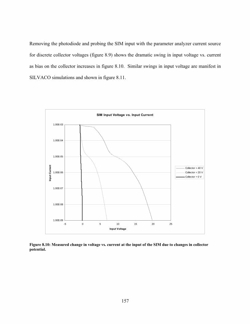
Removing the photodiode and probing the SIM input with the parameter analyzer current source
for discrete collector voltages (figure 8.9) shows the dramatic swing in input voltage vs. current
as bias on the collector increases in figure 8.10. Similar swings in input voltage are manifest in
SILVACO simulations and shown in figure 8.11.
SIM Input Voltage vs. Input Current
1.00E-09
1.00E-08
1.00E-07
1.00E-06
1.00E-05
1.00E-04
1.00E-03
-5 0 5 10 15 20 25
Input Voltage
Inpu
t Cur
rent Collector = 40 V
Collector = 20 V
Collector = 0 V
Figure 8.10: Measured change in voltage vs. current at the input of the SIM due to changes in collector potential.
157

Simulated SIM Input Voltage vs. Current
0.00E+00
2.00E-04
4.00E-04
6.00E-04
8.00E-04
1.00E-03
1.20E-03
-2 0 2 4 6 8
Input Voltage
Inpu
t Cur
rent
Collector=40 VCollector=20 VCollector=0 V
Figure 8.11: Simulated change in voltage vs. current at the input of the SIM due to changes in collector potential from SILVACO. Substrate doping concentration 1e14 cm-3.
The abnormally large change in voltage necessary to change current at the input is the
cause of higher than expected input resistance. Of further insight is the fact that while CIBL is
seen in simulation, it appears to have no effect in simulations involving frequency response
measurement. This is primarily due to the lack of capacitance in the SIM. Simulated SIMs
manifest capacitances in the femto-Farad range. Consequently the response time required for a
voltage change at the input was quite small due to an absence of significant capacitance.
Figure 8.12 shows the measured input resistance of the SIM with respect to input current
for several different bias voltages on the collector. Closer examination reveals that the resistance
induced by the collector is fairly constant a wide range of input currents at each bias point.
158

SIM Input Resistance vs. Input Current
10
100
1000
10000
100000
1E+06
1E+07
1E+08
1E+09
1E+10
1E+11
1.00E-08 1.00E-07 1.00E-06 1.00E-05 1.00E-04
Input Current (A)
Res
ista
nce
(Ohm
s)
40 V
20 V
0 V
Theory
Figure 8.12: SIM input resistance and corresponding input current for collector voltages of 0, 20, and 40 volts. The theory line represents the theoretical kT/I resistance of the junction.
8.7 Elimination of Collector Induced Effects on the Input
Methods to eliminate CIBL are most easily discovered by examining methods used to
eliminate or reduce DIBL. Other methods inherent in devices which do not experience such field
effects also provide possible insights.
Several features make SIMs and MOSFETS susceptible to barrier lowering. The low
doping of the region between the source and drain in a MOSFET or input and collector in a SIM
are necessary and desirable for different reasons. In the case of the MOSFET, the low doping
allows the region beneath the gate to be quickly inverted, thus allowing the formation of an
159

electron channel between source and drain. In the case of the SIM the light bulk doping allows
the formation of a large, high field depletion region between the input and collector which
provides the mechanism for impact ionization. DIBL in MOSFETs is most easily controlled
increasing the doping in the channel between the source and drain, however a trade off is that the
gate oxide must also be decreased to still rapidly deplete the channel [65]. In the case of the
SIM, an increase in bulk doping decreases the field uniformity of the multiplication region
potentially causing less multiplication gain and increased noise.
In reality it is not necessary to dope the entire region between the input and collector.
The only region of concern is the pn junction on the input. Placing a heavily doped p jacket
around the n well input would most likely provide the barrier necessary to withstand high
collector voltages. In such a case, the SIM would resemble something the structure seen in
figure 8.13.
One reason why such confidence is placed in such a simple solution is from CIBL tests
run on npn BJTs in a common base configuration. The narrow base in the BJT is heavily doped
to allow better electron transport and yet easily withstood collector voltages well in excess of 40
volts. SIMs which received a .5 mircon deep boron implant at 1e16 cm-3 and 1e17 cm-3
exhibited improved resistance to CIBL as well. However, because the implant dose was over the
entire surface, they formed a junction with the collector which caused premature breakdown in
the case of the 1e17 cm-3 doping. Furthermore none of these boron implanted SIMs exhibit
gain.
Simulations of the structure seen in figure 8.13a in Silvaco shows that implementation of
a heavily doped p-type jacket around the input keeps the input voltage from swinging relative to
collector voltage.
160

Figure 8.13: A surface SIM that potentially resists barrier lowering due to the collector at the input. a) The P+ doptant acting as a jacket around the n-well input b) keeps the built in voltage θbi from being affected by changes in the collector voltage. c) Simulated input current vs. input voltage in Silvaco for the structure seen in a).
161

The simulated change in input voltage with respect to input current for different collector
voltages is seen in figure 8.13c.
8.8 P-Jacket Acceptor Concentration
The dopant necessary to protect the input from the field generated by the collector can be
calculated by realizing that the field necessary to consume a dopant volume is given by
s
DAWqNEε
= ,
where E is the electric field NA the donor dopant, WD the jacket width and εs the silicon
permittivity. Since the field at which breakdown occurs in silicon is roughly 3x10⁵ V/cm, the
dopant must be strong enough to withstand such a field so that breakdown occurs before jacket
depletion. Substituting in the necessary values to equation 8.27 and solving for NA gives
DA W
xN121097.1
= .
Thus the donor density required depends on the width of the jacket. The doping required in the
jacket is not unrealistically high. Assuming the jacket width to be as narrow as 100 nm requires
an acceptor concentration of roughly 1x10¹⁹ atoms/cm2. The assumptions involved in achieving
this number are quite robust. First it assumes the epitaxial region of the SIM to be completely
intrinsic. In this way the field is quite large and uniform in magnitude from collector to input.
Since the highest field region is usually several microns away from the input, these numbers
assume that the input and the collector and adjacent to one another.
162

8.9 Conclusion
The derivation of SIM input resistance for a broad range of mixed currents indicates a
significant improvement in frequency provided that input barrier lower caused by the collector
are mitigated. Despite the effects of CIBL a mixed current injection scheme shows improvement
when compared to a purely AC input signal. Frequency response in a mixed current scheme will
further improve as the effects of CIBL are mitigated through jacket doping of the input.
163

164

9 CONCLUSION
9.1 Introduction
The SIM was originally envisioned as a low noise current amplifier to be integrated into
long and short haul fiber optic systems. This advantage would forgo the need for epitaxially
grown APDs which incorporate absorption and multiplication regions into the same device.
Rather, optimization of detection and multiplication could be done separately. Naturally, such a
realization would significantly reduce costs and improve performance. While implementation of
the SIM in such systems may not be a reality given current physical limitations, many systems
exist which could benefit from the SIM, especially as further improvements to the gain
mechanism and possible breakthroughs in frequency response are realized.
9.2 Future SIM Work
9.2.1 Substrate Current Injection
A critical factor in improving the SIM is the AC gain. An improvement in gain would
allow for detection of smaller input signals. Smaller AC inputs would cause less swing on the
input voltage and allow for a higher frequency response. As discussed previously in Chapter 6,
confinement and control of high fields is critical to improving gain. While implementing a
buried oxide structure with circular pedestals has improved gains, only so much can be expected
in a scenario where electrons ionize at the surface of the device. If further improvements in gain
165

are to be expected then the impact ionization must occur in the bulk of the semiconductor. This
can be accomplished by moving the input to the substrate and leaving the collector on the
surface. Hole collection would have to be moved to the surface. An illustration of such a device
is seen in figure 9.1.
Figure 9.9.1: SIM where electrons are injected from the substrate.
166

In such a device, a heavily n doped wafer would need a slightly p doped epitaxial region grown
on top of it. Under operation, the collector would be reverse biased with respect to the ring style
P+ hole sink doped into the epitaxial layer. A significant reverse bias would also exist between
the collector and input at the substrate. Thus the field exerted at the collector is split between the
substrate and collector ring. This depletes the lightly doped epitaxial region beneath the
collector and creates a high impact ionization region. Doping of the collector should also be
changed to produce the most uniform field to injected electrons to promote uniform impact
ionization. The greatest challenge to this design is guarding against premature device breakdown
on the surface between the collector and hole sink. Here an element used commonly in APDs is
implemented. By incorporating a heavily n doped floating guard ring between the collector and
hole sink, much of the surface field strength is dissipated with the ring.
Creating a substrate injection SIM involves several doping steps, the most unusual being
the epitaxial growth of a different type of silicon than the substrate. However, the need for
buried oxide devices and circular pedestals to confine electrons within high field regions is no
longer necessary. All the confinement can be done without dry etching or three dimensional
structures on the silicon surface.
9.2.2 Resonant Tunneling Injection
Resonant tunneling injection is another possibility to improve SIM frequency response.
While most resonant tunneling diodes require epitaxial growth of different bandgap
semiconductors to create the necessary quantum well, a MIIM (Metal Insulator Insulator Metal)
diode could be made by depositing two dielectrics of selected bandgap materials on the silicon
surface. A metal layer on top of these dielectrics would effectively create a MIIS (Metal
Insulator Insulator Semiconductor) resonant tunneling diode. By using a resonant tunneling
167

diode, electrons could tunnel into the depletion region of the SIM instead of relying on
thermionic emission or diffusion. This method, has undergone some theoretical testing, but is
for the most part untested. Since a resonant tunneling structure is still diode, the IV
characteristics are still diode-like. However, a resonant tunneling diode turn on is much faster.
This is manifest in the IV curve by a steeper increase in current vs. voltage. Thus the voltage
across the diode changes less with input current than a conventional diode. Consequently,
floating voltage is decreased, and input resistance along with it. This change in the physics of
injecting current into the SIM may greatly improve frequency response.
9.2.3 Noise and Sensitivity
While several references to operational noise have been made in this work, they are with
reference to silicon in general or a qualitative observation of the SIM function. Actual quantities
measurements of excess noise with respect to gain have not be made. A most interesting factor,
which could be determined with such measurements, would be to discover what effect impact
ionization near the surface has on excess noise.
Early in SIM research, several tests were conducted to determine the sensitivity of the
SIM. However, these tests were all conducted using a DC input current with an HP/Agilent 4156
semiconductor parameter analyzer. While these tests proved instructive, it is likely they tell only
part of the story. It is very possible that just as gain, AC and DC measurements are different. In
the case of sensitivity, an AC signal creates more resistance in the SIM because of the change in
current. Thus the sensitivity will most likely decrease as electrons waiting in enter the SIM
recombine due to traps or recombination centers in the silicon. This is merely a theory as no AC
sensitivity work is yet to be undertaken.
168

9.3 SIM Applications
Despite the low frequency response of the SIM, several applications exist which could
benefit from its low noise current amplification properties. It is also important to realize that
operating the SIM in a different regime can significantly increase the frequency response. In a
regime where the SIM input is voltage driven, frequency response increases. This is because the
voltage at the node is no longer governed by the current flowing through it, rather the current is
governed by set voltages from an external voltage source. The nature of this voltage source is
undetermined. It is also very probable that such a voltage source does not need low noise current
amplification. In cases of current amplification from current sources, several lower frequency
application exist which could benefit from SIM style amplification. In the realm of
optoelectronics, semiconductor CCDs with bandgaps too low to create avalanche multiplication
internally could be integrated onto a silicon chip of SIMs. These SIMs would take the current
input from the photodiodes and perform the initial amplification. Such a configuration would
easily operate at video speeds.
For still photography, SIMs with a gain of 8 would improve the sensor sensitivity by 3
stops. In conventional CCD cameras, increasing the sensitivity by one stop means that the light
sample taken by the CCD is cut in half. A smaller sampling time cuts the collected current in
half. Bringing the final image up to full exposure requires double the amplification. This is
accomplished by transistor amplifiers. The noise introduced from the amplification leads to
degradation of the final image. Further reduction in CCD sampling time requires further
amplification of the current and creates more and more noise which degrades the image. Pre-
amplification with the SIM would allow shorter exposures with less amplifier noise in the final
image.
169

A non-optical application for which the SIM bandwidth is already perfectly suited is as a
microphone preamplifier. Several different microphones exist, and the physics for each of them
vary. Consequently, the SIM would not be suitable for condenser or electret condenser
microphones which measure membrane capacitance to convert waves from acoustic to electric.
Figure 9.9.2: Two SIMs pre amplify current generated from a microphone before amplification in a summing amplifier.
170

Crystal microphones which measure voltage across piezo-electric crystals are also poorly suited
for the SIM. However, dynamic and ribbon microphones are well suited as inputs to the SIM.
These microphones generate current proportional to acoustic waves as these acoustic waves
move a metallic transducer within a magnetic field. The output current from the transducer is
then fed into the SIM which acts as a low noise preamplifier. This would improve the quality of
recordings by reducing the amount of amplifier noise present in the recording. One problem
with amplification of a typical AC signal of this fashion is that the SIM in its current state only
amplifies electrons. Injected holes recombine in the n well at the input. Thus two SIMs are
necessary to capture the entire signal one on each end. Figure 9.2 illustrates two SIMs used to
amplify current from a dynamic microphone. As shown, output current from the SIMs is then
summed and amplified. Such a configuration would greatly enhance the sensitivity of dynamic
and ribbon microphones and thus make them more useful in many applications.
9.4 Conclusion
While much of this work is wholly untested and documented, this is what makes it future
work. Current understanding of the SIM justifies many of the assumptions made in these devices
or operating modes. Doubtless other useful applications also exist. This chapter gives a taste of
just a few of the many possibilities
In conclusion of this work as a whole, several challenges exist which reduce the speed at
which a change in current be can electrically injected into a junction of a semiconductor. This
fact explains much of the frequency response difficulties of the SIM when operated with a
photodiode with low input currents. However, tremendous discovery has accompanied the
research involved in developing the SIM. The limiting factor which physically limits the SIM
171
frequency response has been discovered and documented. Reduction of CIBL will allow
physical models to better match theoretical ones. The need to control and confine geometries
within the high field regions of the SIM have also permitted increased gains. And increased
feature size of SIM devices has significantly reduced parasitic space charge resistances to
increase gain without reducing frequency response. A clear understanding of the physics of a
device leads to further innovation. Some of this innovation has been discussed, but most of it is
yet to flourish.
172

10 REFERENCES
[1] E. J. Lerner, "Photomultiplier tubes stay the course," Laser Focus World, vol. 37, pp. 151, 06. 2001. [2] J. R. Chelikowsky and M. L. Cohen, "Nonlocal pseudopotential calculations for the electronic structure of eleven diamond and zinc-blende semiconductors," Phys. Rev., vol. 14, pp. 556, 1976. [3] H. Lee, "Solid-State Impact-Ionization Multiplier," 2006. [4] R. B. Emmons, "Avalanche-Photodiode Frequency Response," J. Appl. Phys., vol. 38, pp. 3705-3714, August 1967. 1967. [5] P. P. Webb, R. J. McIntyre and J. Conradi, "PROPERTIES OF AVALANCHE PHOTODIODES," RCA (Radio Corporation of America) Review, vol. 35, pp. 234-278, 1974. [6] S. Wang, R. Sidhu, X. G. Zheng, X. Li, X. Sun, A. L. Holmes Jr. and J. C. Campbell, "Low- noise avalanche photodiodes with graded impact-ionization-engineered multiplication region," Photonics Technology Letters, IEEE, vol. 13, pp. 1346-1348, 2001. [7] S. M. Sze and G. Gibbons, "Effect of Junction Curvature on Breakdown voltages in Semiconductors," Solid-State Electron., vol. 9, pp. 831-845, April 21, 1966. 1966. [8] C. Parks and D. Losee, "Large area interline CCD with low dark current," in Proceedings of SPIE, 2003, pp. 167-175. [9] E. R. Fossum, "Digital camera system on a chip," Micro, IEEE, vol. 18, pp. 8-15, 1998. [10] N. S. Nightingale, "A new silicon avalanche photodiode photon counting detector module for astronomy," Experimental Astronomy, vol. 1, pp. 407-422, Nov 1990. 1990. [11] D. Yin, D. W. Deamer, H. Schmidt, J. P. Barber and A. R. Hawkins, "Single-molecule detection sensitivity using planar integrated optics on a chip," Opt. Lett., vol. 31, pp. 2136-2136-2138, 2006.
173

[12] D. Yin, E. Lunt, M. I. Rudenko, D. W. Deamer, A. R. Hawkins and H. Schmidt, "Planar optofluidic chip for single particle detection, manipulation, and analysis," Lab on a Chip, vol. 7, pp. 1171-1171-1175, 2007. [13] R. P. Davey, P. Healey, I. Hope, P. Watkinson, D. B. Payne, O. Marmur, J. Ruhmann and Y. Zuiderveld, "DWDM reach extension of a GPON to 135 km," Lightwave Technology, Journal of, vol. 24, pp. 29-31, 2006. [14] M. D. Seltzer, M. S. Hendrick and R. G. Michel, "PHOTOMULTIPLIER GATING FOR IMPROVED DETECTION IN LASER-EXCITED ATOMIC FLUORESCENCE SPECTROMETRY," Anal. Chem., vol. 57, pp. 1096-1100, 1985. [15] T. O. Tumer, B. Holbrook, J. Linn, J. Lizarazo, G. Mohanty, U. Mohideen, P. Murray, H. Tom, M. Tripathi, G. Xing and J. Zweerink, "New detector for observing very high energy gamma-rays from celestial sources," in X-Ray and Gamma-Ray Instrumentation for Astronomy XII, 2002, pp. 106-114. [16] E. Hergert, "Photomultiplier tubes count photons," Laser Focus World, vol. 33, pp. 129, 11. 1997. [17] E. J. Lerner, "Photomultiplier tubes offer high-end sensitivity," Laser Focus World, vol. 32, pp. 87, 07. 1996. [18] C. D'Ambrosio, F. De Notaristefani, H. Leutz, D. Puertols and E. Rosso, "X-ray detection with a scintillating YAP-window hybrid photomultiplier tube," Nuclear Science, IEEE Transactions on, vol. 47, pp. 6-12, 2000. [19] W. Paper. Noise in silicon photomultipliers and vacuum photomultiplier tubes. 2008(10/02), pp. 20. Available: http://www.sensl.com/pdfs/SPM_Tech_App_Notes/WP_Noise.pdf [20] S. M. Sze and K. K. Ng, Physics of Semiconductor Devices. ,3rd ed.Holbokem, New Jersey: John Wiley & Sons, Inc, 2007, pp. 815. [21] R. J. McIntyre, "A new look at impact ionization-Part I: A theory of gain, noise, breakdown probability, and frequency response," Electron Devices, IEEE Transactions on, vol. 46, pp. 1623-1631, 1999. [22] P. Yuan, K. A. Anselm, C. Hu, H. Nie, C. Lenox, A. L. Holmes, B. G. Streetman, J. C. Campbell and R. J. McIntyre, "A new look at impact ionization-Part II: Gain and noise in short avalanche photodiodes," Electron Devices, IEEE Transactions on, vol. 46, pp. 1632-1639, 1999. [23] H. Daulet, P. Deschamps, B. Dion, A. D. MacGregor, D. MacSween, R. J. McIntyre, C. Trottier and P. P. Webb, "Photon counting techniques with silicon avalanche photodiodes," Applied Optics, vol. 32, pp. 3894-3894-3900, 1993.
174

[24] G. S. Buller, S. Pellegrini, R. E. Warburton, J. S. Ng, L. J. Tan, A. Krysa, J. P. R. David and S. Cova, "Semiconductor Avalanche Diode Detector for Quantum Cryptography," IEEE LEOS Newsletter, vol. 20, pp. 20-20-24, October 2006. 2006. [25] S. Cova, A. Tosi, A. Gulinatti, F. Zappa and M. Ghioni, "Avalanche Diodes and Circuits for Infared Photon Counting and Timing: Retrospect and Prospect," IEEE LEOS Newsletter, vol. 20, pp. 25-25-28, October 2006. 2006. [26] Z. L. Yuan, A. R. Dixon, J. F. Dynes, A. W. Sharpe and A. J. Shields, "Gigahertz quantum key distribution with InGaAs avalanche photodiodes," Appl. Phys. Lett., vol. 92, pp. 201104, 19 May 2008. 2008. [27] A. H. Sommer, "The element of luck in research--photocathodes 1930 to 1980," Journal of Vacuum Science & Technology A: Vacuum, Surfaces, and Films, vol. 1, pp. 119-124, April 1 1983. 1983. [28] A. R. Hawkins, W. Wu, P. Abraham, K. Streubel and J. E. Bowers, "High gain-bandwidth- product silicon heterointerface photodetector," Appl. Phys. Lett., vol. 70, pp. 303-305, January 20, 1997. 1997. [29] K. G. McKay and K. B. McAfee, "Electron Multiplication in Silicon and Germanium," Phys. Rev., vol. 91, pp. 1079, May, 29 1953. 1953. [30] F. Capasso, "Physics of avalanche photodiodes," in Semiconductors and Semimetals , vol. 22, W. T. Tsang, Ed. New York: Academic Press, 1985, pp. 2-2-172. [31] P. A. Wolff, "Theory of Electron Multiplication in Silicon and Germanium," Phys. Rev., vol. 95, pp. 1415, September, 15 1954. 1954. [32] J. Maserjian, "Determination of Avalanche Breakdown in pn Junctions," J. Appl. Phys, vol. 30, pp. 1613-1614, 1959. [33] W. Fulop, "Calculation of Avalanche Breakdown Voltages of Silicon p-n Junctions," Solid- St. Electron., vol. 10, pp. 39, 1967. [34] R. Van Overstraeten and H. De Man, "Measurment of the Ionization Rates in Diffused Silicon p-n Junctions," Solid-St. Electron., vol. 13, pp. 583-608, 1970. [35] M. H. Woods, W. C. Johnson and M. A. Lampert, Solid-State Electron., vol. 16, pp. 381, 1973. [36] K. G. McKay, "Avalanche Breakdown in Silicon," Phys. Rev., vol. 94, pp. 877, 1954. [37] G. E. Stillman and C. M. Wolfe, "Avalanche photodiodes," in Semiconductors and Semimetals ,First Edition ed., vol. 12, R. K. Willandson and A. C. Beer, Eds. New York: Academic Press, 1977, pp. 291-291-393.
175

[38] F. Ma, X. Li, J. C. Campbell, J. D. Beck, C. Wan and M. A. Kinch, "Monte Carlo simulations of Hg[sub 0.7]Cd[sub 0.3]Te avalanche photodiodes and resonance phenomenon in the multiplication noise," Appl. Phys. Lett., vol. 83, pp. 785-787, July 28, 2003. 2003. [39] M. A. Kinch, J. D. Beck, C. F. Wan, F. Ma and J. C. Campbell, "HgCdTe electron avalanche photodiodes," J. Electron. Mater., vol. 33, pp. 630-639, June 2004. 2004. [40] J. Beck, C. Wan, M. Kinch, J. Robinson, P. Mitra, R. Scritchfield, F. Ma and J. Campbell, "The HgCdTe Electron Avalanche Photodiode," IEEE LEOS Newsletter, vol. 20, pp. 8- 12, October 2006. 2006. [41] J. C. Campbell, S. Demiguel, Feng Ma, A. Beck, Xiangyi Guo, Shuling Wang, Xiaoguang Zheng, Xiaowei Li, J. D. Beck, M. A. Kinch, A. Huntington, L. A. Coldren, J. Decobert and N. Tscherptner, "Recent advances in avalanche photodiodes," Selected Topics in Quantum Electronics, IEEE Journal of, vol. 10, pp. 777-787, 2004. [42] T. Al-Attar and T. H. Lee, "Monolithic integrated millimeter-wave IMPATT transmitter in standard CMOS technology," Microwave Theory and Techniques, IEEE Transactions on, vol. 53, pp. 3557-3561, 2005. [43] H. Lee and A. R. Hawkins, "Solid-state current amplifier based on impact ionization," Appl. Phys. Lett., vol. 87, pp. 073511, 15 August 2005. 2005. [44] H. Lee, J. L. Beutler and A. R. Hawkins. (2005, Surface structure silicon based impact- ionization multiplier for optical detection. Opt Express 13pp. 8760-8760-8765. [45] H. Lee, J. L. Beutler and R. Hawkins, "High gain effects for solid-state impact-ionization multipliers," Quantum Electronics, IEEE Journal of, vol. 42, pp. 471-476, 2006. [46] J. L. Beutler, C. S. Clauss, M. S. Johnson, A. R. Hawkins, M. D. Jack, G. R. Chapman and K. Kosai, "Frequency response of solid-state impact ionization multipliers," J. Appl. Phys., vol. 101, pp. 023117, January 2007. 2007. [47] S. M. Sze, Physics of Semiconductor Devices. ,2nd ed.New York: John Wiley and Sons, 1981, pp. 868. [48] M. Morschbach, S. Diemer, M. Oehme and E. Kasper, "Design of a Monolithic 79 GHz Rectenna with MOTT Diodes," Topical Meeting on Silicon Monolithic Integrated Circuits in RF Systems Digest of Papers, pp. 122-122- 125, 2003. [49] W. Monch, "Barrier heights of real Schottky contacts explained by metal-induced gap states and lateral inhomogeneities," J. Vac. Sci. Technol. B, vol. 17, pp. 1867-1876, July 1999. 1999.
176

[50] Kyuwoon Hwang and D. H. Navon, "Breakdown voltage optimization of silicon p-π-v planar junction diodes," Electron Devices, IEEE Transactions on, vol. 31, pp. 1126- 1135, 1984. [51] J. K. Mishra, A. K. Panda and G. N. Dash, "An extremely low noise heterojunction IMPATT," Electron Devices, IEEE Transactions on, vol. 44, pp. 2143-2148, 1997. [52] R. J. McIntyre, "Multiplication noise in uniform avalanche diodes," Electron Devices, IEEE Transactions on, vol. 13, pp. 164-168, 1966. [53] K. Nishida, K. Taguchi and Y. Matsumoto, "InGaAsP heterostructure avalanche photodiodes with high avalanche gain," Appl. Phys. Lett., vol. 35, pp. 251-253, August 1, 1979. 1979. [54] P. P. Webb, "Measurements of Ionization Coefficients in Silicon at Low Electric Fields," Solid-St. Electron., vol. 16, pp. 1189, 1973. [55] W. J. Kindt, N. H. Shahrjerdy and H. W. van Zeijlv, "A silicon avalanche photodiode for single optical photon counting in the Geiger mode," Sensors and Actuators, vol. 60, pp. 98-102, 1997. [56] D. Ritter, K. Weiser and E. Zeldov, "Steady-state photocarrier grating technique for diffusion-length measurement in semiconductors: Theory and experimental results for amorphous silicon and semi-insulating GaAs," J. Appl. Phys., vol. 62, pp. 4563, December 1, 1987. 1987. [57] C. Canali, G. Majni, R. Minder and G. Ottaviani, "Electron and hole drift velocity measurements in silicon and their empirical relation to electric field and temperature," Electron Devices, IEEE Transactions on, vol. 22, pp. 1045-1047, 1975. [58] M. Saritas and H. D. McKell, "Comparison of minority-carrier diffusion length measurements in silicon by the photoconductive decay and surface photovoltage methods," J. Appl. Phys., vol. 63, pp. 4561-4567, May 1, 1988. [59] M. Ohring, Materials Science of Thin Films, Deposition & Structure. ,Second ed.USA: Academic Press, 2002, pp. 794-34. [60] E. Hökelek and G. Y. Robinson, "Aluminum/Nickel Silicide Contacts on Silicon," Thin Solid Films, vol. 53, pp. 135-135-140, April 25, 1978. 1978. [61] L. Jianwen and P. Hongfang, "The Effect of Composition on the Barrier Height and Contact Resistance of TixW1-x/Si Contacts," J. Electron. Mater., vol. 16, pp. 199-199-201, 1987. [62] S. S. Cohen, P. A. Piacente, G. Gildenblat and D. M. Brown, "Platinum silicide ohmic contacts to shallow junctions in silicon," J. Appl. Phys., vol. 53, pp. 8856-8852-8862, August 1982. 1982.
177

[63] R. C. Jaeger, Microelectronic Circuit Design. ,2nd ed. ed.New York: McGraw-Hill Higher Education, 2004. [64] Y. Taur and T. H. Ning, Fundamentals of Modern VLSI Devices. New York: Cambridge University Press, 2002, pp. 469. [65] M. Lundstrom, "APPLIED PHYSICS: Enhanced: Moore's Law Forever?" Science, vol. 299, pp. 210-211, January 10. 2003.
LIST OF PUBLICATIONS
1. Michael S. Johnson, Joshua L. Beutler, Alan P. Nelson, and Aaron R. Hawkins, “SiO2
Barriers for increasing gain events in Solid-state Impact-ionization Multipliers,” IEEE Journal of Quantum Electronics vol. 45, 1068-1073, (2009).
2. Michael S. Johnson, Joshua L. Beutler, Alan P. Nelson, and Aaron R. Hawkins, “Solid-state
Impact-ionization Multiplier with PN Junction Injection Node,” IEEE Journal of Transactions on Electron Devices vol.56, 1360-1363, (2009).
3. Joshua L. Beutler, Carleton S. Clauss, Michael S. Johnson, and Aaron R. Hawkins,
“Frequency Response of Solid-State Impact-Ionization Multipliers,” Journal of Applied Physics vol. 101, 023117 (2007).
4. Hong-Wei Lee, Joshua L. Beutler, and Aaron R. Hawkins, “High Gain Effects for Solid-State
Impact-Ionization Multipliers,” IEEE Journal of Quantum Electronics vol. 42, 471-476, (2006).
5. Hong-Wei Lee, Joshua L. Beutler, and Aaron R. Hawkins, “Surface structure silicon based
impact- ionization multiplier for optical detection,” Optics Express vol. 13, 8760-8765, (2005).
6. Aaron R. Hawkins, Ran Wang, Ghassan Sanber, Joshua Beutler, and Stephen M. Schultz,
"Color Pictures Using Dielectric Films," COLOR Research and Application, vol. 30 No. N2, 125-129, (2005)
178

A APPENDIX A. FABRICATION PROCEDURES
A.1 SIM Fabrication Procedure for Rectangular Buried Oxide SIMs
• Use the Wacker wafers with a P+ substrate and a P- EPI layer. Make sure they are not
reclaim wafers because reclaim wafers have no EPI layer left.
A.1.1 Step 1—KOH Etch Mask, and KOH Etching
1) Create the KOH etch mask by growing 1200 Angstroms of thermal oxide on the wafers.
Do it quickly using wet oxide. Make sure the bubbler has a 10:1 ratio of H2O:HCl. This
is always critical. It really helps reduce contamination in the wafer. This is manifest by
an improvement in leakage currents. To grow the oxide. Follow Oxide Growth Chart #1.
2) After oxide growth, dehydrate wafers, apply HMDS and Spin on AZ 2020 at 3000 RPMs.
Soft bake for 60 seconds at 110˚ C on the hotplate. Use N+ well mask and the ISCH
recipe on the south aligner. Only change the exposure time in the ISCH program to 20
seconds.
3) DON’T FORGET the post exposure bake before you develop. Post exposure bake on
hotplate for 60 seconds at 110˚ C.
4) Develop wafer in AZ 300 MIF developer. It usually takes awhile sometimes 3 minutes.
It requires some eyeballing. The easiest way to tell when the resist is developed is that
the small fine tuning alignment marks are developed into the resist.
179

5) Rinse the wafer well and hard bake on the hotplate at 110˚ C for 5 minutes.
6) Do an O2 descum in the Planar Etcher (PE2) for 15 seconds at 50 watts. Then turn the
wafers 180˚ in the PE2 and etch for another 15 seconds at 50 watts.
7) Remove the thermal oxide to create the KOH etch mask by dipping in Buffered Oxide
Etch (BOE) until the surface of the wafer becomes mostly hydrophobic. Then over-etch
for another 60 seconds. This over-etching will cause undercutting on the resist and help
increase in spacing between the wells thus making devices of smaller spacing useful.
8) Rinse the wafer in De-Ionized Water (DI Water) for at least 60 seconds.
9) Remove the remaining resist in NMP on a hotplate set to 65˚ C. Allow the NMP about
20 minutes to fully remove the resist. Then rinse in DI Water BEFORE using Isopropyl
Alcohol (IPA) or Acetone.
10) Start the KOH etching process by adding DI Water to the KOH etching bath. Fill the
water to the level of the KOH in the glassware.
11) Turn on the heat to the bath by powering up the Modutek hot bath controller. The
temperature should be preset to 50˚ C. This is done by pressing the “Timer” button
followed by the “Reset” button on the Modutek controller. Any additional information
on the controller and bath can be found at
http://www.ee.byu.edu/cleanroom/Hot_Pot.phtml a PDF of the manual can be found at
http://www.ee.byu.edu/cleanroom/Online_Manuals/Hot_Pot%20Controller.pdf
12) Make sure your KOH solution is about 75% KOH solution from the container and 25%
DI Water by volume. Water is important in this whole reaction. Without sufficient
amounts of water, the wafer will become pitted and not etch smoothly.
180

13) Allow about 60 minutes for the bath and KOH to stabilize in temperature. Etch wafers
one at a time. Etch for 10 minutes and then check the etching progress with the
profolometer. The target height is 3 um. Typically etch to about 3.2 um.
14) After proper pedestal height is achieved rinse the KOH solution off. It is very viscous.
Rinse in DI Water for 10 minutes.
15) Etch off remaining KOH etch mask and backing oxide on wafers in BOE.
16) Rinse and get ready for oxide growth.
A.1.2 Step 2—Oxide Growth and Diffusion Mask Planarization
1) Do a 3 minute, 50 watt descum in the PE2 on the backs and then on the front of the
wafers.
2) Quick dip in BOE and rinse in DI Water.
3) Grow 5000 Angstroms of thermal oxide in tube furnace according to Oxide Growth Chart
#2. Do not forget the 10:1 DI Water:HCl ratio in the bubbler.
4) After oxide growth, dehydrate wafers apply HMDS and spin on SU-8 3005. BE SURE
TO USE THE SMALL CHUCK WHEN YOU SPIN TO KEEP SU8 OFF THE BACK
OF THE WAFER. Spin speed for 5000 RPM with a ACL of 1000 for 60 seconds. Then
bake for 5 minutes at 65˚ C then ramp to 95˚ C and hold for another 5 minutes. Remove
wafer and cure resist by exposing wafer under the south aligner for 60 seconds.
5) Hard bake resist with 5 minutes at 65˚ C then ramp to 95˚ C and hold for 5 minutes.
Then ramp to 110˚ C and hold for 5 minutes then to 150˚ C for 5 minutes THEN ramp to
200˚ C for 10 minutes. Then turn off hotplate an allow wafers to cool on cooling hotplate
until hotplate temperature is below 90˚ C.
6) Remove wafers from hotplate and get ready to polish with the CMP.
181

7) The CMP directions are found at http://www.ee.byu.edu/cleanroom/cmp.phtml
8) Use the SU8-5 recipe in the CMP and the Eminess Ultrasol A-15 slurry. It works most
excellently to polish SU8. Dilute the slurry about 10:1 or 5:1 DI Water to slurry. The 5
gallon dilute slurry bucket is labeled “SIM Group A-15 DIL.” The concentrated slurry
bucket is labeled “SIM Group.”
9) Be sure to stir the diluted slurry while polishing to that the mixture does not settle.
10) Polish the SU8 down until the tops of the devices pedestals have the oxide polished down
to bare silicon.
11) Rinse polished wafers in DI Water. Place in Nanostrip on a hot plate at 90˚ C for at least
1 hour.
A.1.3 Step 3—Diffusion
1) Remove wafers from Nanostrip. Rinse thoroughly in DI Water. Dehydration bake the
wafers in the oven at 150˚ C for 30 minutes. Remove wafers and do a quick BOE dip.
Rinse in DI Water and place in the PE2 chamber and vacuum down. Do NOT activate
the plasma. This vacuum chamber is merely to pull water out of the wafer without
growing an oxide on the wafer surface.
2) Remove the Honeywell P-8548 Spin on Dopant (SOD) from the refrigerator at least 4
hours before applying the SOD to the wafers.
3) Use Pipets and the Headway spinner to apply SOD. Use a pipet to cover 80% of the
wafer with SOD then spin the wafer at 500 RPM for about 2 seconds and slowly ramp to
3000 RPM. After 20 seconds, remove the wafer and place it on a hotplate at 150˚ C for
60 seconds.
4) Diffuse wafers in the furnace according to Diffusion Chart #1.
182

5) Immediately etch remaining SOD from the wafers after they come out of the furnace. It
should only take about 45 seconds in BOE. Then rinse in DI Water.
6) You can check if the glass is removed by applying voltage to the N+ wells and substrate
and observing the current.
A.1.4 Step 4—Metallization
1) Dehydrate wafers, apply HMDS, and a thick layer of AZ 3330 photoresist. This is done
by using the small chuck on the spinner so the resist does not seep onto the back of the
wafer and using a max spin speed of 3000 RPM with ACL of 500. This helps the resist
clear the pedestals.
2) Soft bake the wafer for 12 minutes at 90˚ C on a hotplate. Expose on the south aligner
with metal mask on the ISCH program. Edit the program and change the exposure time
to 20 seconds.
3) Develop in AZ 300 MIF developer. This takes several minutes. Verify development
under the microscope and ensure that the resist has fully developed
4) Descum in the PE2 30 seconds at 50 watts and turn the wafers 180˚ and do another 30
second descum at 50 watts.
5) Prepping the wafer for metallization needs to be done right before placing the wafer into
the sputterer.
6) Quick dip in BOE and rinse in DI water. Then dip into a 1:1 Di Water:HCl solution for
30 seconds. Rinse and dry and place directly into the sputterer.
7) Pump the sputter to 4 e-6 torr. Then deposit TiW on Cathode 3 DC sputtering at 150 mA
current for 1000 seconds. This gives about 70 nm for TiW as a barrier metal.
183

8) Vent the sputterer and place the wafer into the thermal evaporator and deposit 1 um of
aluminum on top of the TiW.
9) Vent the evaporator and flip the wafers to deposit 300 nm of aluminum on the back side.
10) Lift off the front metal in acetone. This requires a fair amount of scrubbing with a foam
tip to remove the metal. Rinse in IPA and acetone and blow dry.
11) Anneal in forming gas environment at 450˚ C for 30 minutes. Run the forming gas on
full flow on the pin gauge.
12) The wafer is finished.
A.2 SIM Fabrication Procedure for Circular Pedestal SIMs
• Use the Wacker or Montco wafers with a P+ substrate and a P- EPI layer. Make sure
they are not reclaim wafers because reclaim wafers have had the EPI layer polished off.
A.2.1 Step 1—RIE, ICP Etching
1) Spin SU-8 2002 onto the wafers and soft bake. Then expose the wafers with the first N+
well mask for 8 seconds. Don’t forget the post-exposure bake!
2) Develop in SU-8 developer and rinse in IPA and then blow dry.
3) Descum wafers at 150 W for 2 minutes in the PE2.
4) RIE etch wafers in the Trion etcher one at a time. Each wafer requires several recipes to
etch properly. Training is required!
5) Make sure the Trion chamber is clean by running the “Clean-New” recipe for six minutes
on both steps.
184

6) Load the wafer and etch it with the “Evan-Bosch-Si3” etch. This etch take about 20
minutes and must be run twice to achieve a pedestal height of roughly 2.5 um.
7) Following the etching of one wafer, run the “Clean-New” etch as described previously to
clean the chamber.
8) Load the etched wafers into the PE2 and do another descum etch at 150 W for 2 minutes.
This removes any teflons that have built up on the wafer.
A.2.2 Step 2—Oxide Growth and Diffusion Mask Planarization
1) Quick dip in BOE and rinse in DI Water.
2) Grow 5000 Angstroms of thermal oxide in tube furnace according to Oxide Growth Chart
#2. Do not forget the 10:1 DI Water:HCl ratio in the bubbler.
3) After oxide growth, dehydrate wafers apply HMDS and spin on SU-8 3005. BE SURE
TO USE THE SMALL CHUCK WHEN YOU SPIN TO KEEP SU8 OFF THE BACK
OF THE WAFER. Spin speed for 5000 RPM with a ACL of 1000 for 60 seconds. Then
bake for 5 minutes at 65˚ C then ramp to 95˚ C and hold for another 5 minutes. Remove
wafer and cure resist by exposing wafer under the south aligner for 60 seconds.
4) Hard bake resist with 5 minutes at 65˚ C then ramp to 95˚ C and hold for 5 minutes.
Then ramp to 110˚ C and hold for 5 minutes then to 150˚ C for 5 minutes THEN ramp to
200˚ C for 10 minutes. Then turn off hotplate an allow wafers to cool on cooling hotplate
until hotplate temperature is below 90˚ C.
5) Remove wafers from hotplate and get ready to polish with the CMP.
6) The CMP directions are found at http://www.ee.byu.edu/cleanroom/cmp.phtml
7) Use the “SU8-5” recipe in the CMP and the Eminess Ultrasol A-15 slurry. It works most
excellently to polish SU8. Dilute the slurry about 10:1 or 5:1 DI Water to slurry. The 5
185

gallon dilute slurry bucket is labeled “SIM Group A-15 DIL.” The concentrated slurry
bucket is labeled “SIM Group.”
8) Be sure to stir the diluted slurry while polishing to that the mixture does not settle.
9) Polish the SU8 down until the tops of the devices pedestals have the oxide polished down
to bare silicon.
10) Rinse polished wafers in DI Water. Place in Nanostrip on a hot plate at 90˚ C for at least
1 hour.
A.2.3 Step 3—Diffusion
1) Remove wafers from Nanostrip. Rinse thoroughly in DI Water. Dehydration bake the
wafers in the oven at 150˚ C for 30 minutes. Remove wafers and do a quick BOE dip.
Rinse in DI Water and place in the PE2 chamber and vacuum down. Do NOT activate
the plasma. This vacuum chamber is merely to pull water out of the wafer without
growing an oxide on the wafer surface.
2) Remove the Honeywell P-8548 Spin on Dopant (SOD) from the refrigerator at least 4
hours before applying the SOD to the wafers.
3) Use Pipets and the Headway spinner to apply SOD. Use a pipet to cover 80% of the
wafer with SOD then spin the wafer at 500 RPM for about 2 seconds and slowly ramp to
3000 RPM. After 20 seconds, remove the wafer and place it on a hotplate at 150˚ C for
60 seconds.
4) Diffuse wafers in the furnace according to Diffusion Chart #1.
5) Immediately etch remaining SOD from the wafers after they come out of the furnace. It
should only take about 45 seconds in BOE. Then rinse in DI Water.
186

6) You can check if the glass is removed by applying voltage to the N+ wells and substrate
and observing the current.
A.2.4 Step 4—Metallization
1) Dehydrate wafers, apply HMDS, and a thick layer of AZ 3330 photoresist. This is
done by using the small chuck on the spinner so the resist does not seep onto the back
of the wafer and using a max spin speed of 3000 RPM with ACL of 500. This helps
the resist clear the pedestals.
2) Soft bake the wafer for 12 minutes at 90˚ C on a hotplate. Expose on the south
aligner with metal mask on the ISCH program. Edit the program and change the
exposure time to 20 seconds.
3) Develop in AZ 300 MIF developer. This takes several minutes. Verify development
under the microscope and ensure that the resist has fully developed
4) Descum in the PE2 30 seconds at 50 watts and turn the wafers 180˚ and do another 30
second descum at 50 watts.
5) Prepping the wafer for metallization needs to be done right before placing the wafer
into the sputterer.
6) Quick dip in BOE and rinse in DI water. Then dip into a 1:1 Di Water:HCl solution
for 30 seconds. Rinse and dry and place directly into the sputterer.
7) Pump the sputter to 4 e-6 torr. Then deposit TiW on Cathode 3 DC sputtering at 150
mA current for 1000 seconds. This gives about 70 nm for TiW as a barrier metal.
8) Vent the sputterer and place the wafer into the thermal evaporator and deposit 1 um
of aluminum on top of the TiW.
187

9) Vent the evaporator and flip the wafers to deposit 300 nm of aluminum on the back
side.
10) Removing metal from a liftoff photoresist mask can be difficult when a planetary is
used. The planetary is necessary to coat the sidewalls of the pedestals. Tape liftoff
on the front of the wafer is most effective. Take a strip of scotch tape long enough to
traverse the wafer and press firmly onto the wafer, then pull off. Repeat this until the
whole wafer has been done.
11) Lift off any remaining metal in acetone. Rinse in IPA and acetone and blow dry.
12) Anneal in forming gas environment at 450˚ C for 30 minutes. Run the forming gas
on full flow on the pin gauge.
13) The wafer is finished.
188
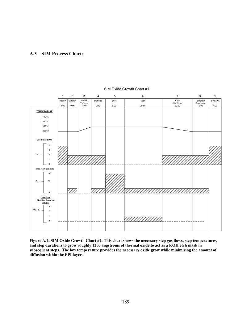
A.3 SIM Process Charts
Figure A.1: SIM Oxide Growth Chart #1: This chart shows the necessary step gas flows, step temperatures, and step durations to grow roughly 1200 angstroms of thermal oxide to act as a KOH etch mask in subsequent steps. The low temperature provides the necessary oxide grow while minimizing the amount of diffusion within the EPI layer.
189

Figure A.2: SIM Oxide Growth Chart #2: This chart shows the necessary step gas flows, step temperatures, and step durations to grow 5000 angstroms of thermal oxide. This oxide acts as an insulator and passivation layer for the SIM.
190

191
Figure A.3: SIM Diffusion Chart #1 for P-8545 Spin on Dopant (SOD): This chart shows the necessary step gas flows, step temperatures, and step durations to diffuse phosphorus into the SIM pedestals to a depth of roughly 1.3 um. It is important that sufficient oxygen is always flowing into the furnace during the diffusioOxygen allows the phosphorus in the SOD to diffuse by turning the phosphoric acid (H3PO4) within thmixture into Phosphorus Pentoxide (P2O5). It is important to completely oxidize all the H3PO4 withSOD otherwise it will form a bond with the silicon that cannot be removed unless it is first oxidiz
n. e
in the ed.
Following diffusion, it is important to immediately dip the wafers in Buffered Oxide Etch (BOE) to completely remove the SOD before the P2O5 reacts with the moisture in the air to form H3PO4.