Frequency multiplier response to spurious signals
9
Frequency multiplier response to spurious signals and its effect on local oscillator systems in millimeter and submillimeter wavelengths Goutam Chattopadhyay *a , Erich Schlecht b , Frank Maiwald b , Robert J. Dengler b , John C. Pearson b , and Imran Mehdi b a California Institute of Technology, 320–47 Caltech, Pasadena, CA 91125 b Jet Propulsion Laboratory, M/S 168–314, 4800 Oak Grove Drive, Pasadena, CA 91109 ABSTRACT Broadband fixed-tuned frequency multipliers in conjunction with broadband power amplifiers driven by fre- quency synthesizers are often used as local oscillator (LO) sources in the millimeter and submillimeter wave heterodyne instrume nts . At these freq uenc ies the mult ipliers use Galliu m Arsenid e (GaAs) based Schott ky varactor diodes as the nonlinear element, and like most other harmonic generators are susceptible to spurious signal interference. The state-of-the-art LO sources in the millimeter and submillimeter wavelengths use MMIC power amplifiers producing in excess of 250 mW of output power in the 100 GHz range, and they are used to drive the subs eque nt multipli er stage s. Because of the high input power environment and the presenc e of noise in the system, the multipliers become vulnerable to spurious signal interference, either through the bias lines or through the RF port. As the spur ious signals propa gate through the multip lier ch ain, they generat e inter-modulation products which might fall in the passband of the heterodyne instrument and seriously degrade its performance. The issues of frequency multiplier response to spurious signal inte rference and its e ffect on local oscillator performance in millimeter and submillimeter wave heterodyne instruments are investigated. Results of numerical harmonic balance simulations and laboratory experiments are presented here, and are found to show good agreement. Keywords: spurious signals, frequency multipliers, millimeter and submillimeter waves 1. INTRODUCTION Currently many new instruments, which are primarily intended for astrophysical observations, are being built at millime ter and submi llimeter wavelengths. Heterodyne receivers (coh erent dete ctor s) are the receivers of choice for many of these instruments. In a heterodyne system, the incomin g radio frequency signa l ( ν RF ) is down-converted to an intermediate frequency signal ( ν IF ) in a mixer pumped by a local oscillator signal ( ν LO ), as sho wn in the simpli fied bloc k dia gram of a he ter odyne receiver in Figure 1. The noise per for man ce of a heterodyne system depen ds prima rily on the noise temperatu re of thes e fron t-end components. At millimeter and submillimeter wave lengths, the first front-end component is a mixer, often cryogenic, such as superconductor insulator superconductor (SIS) or hot electron bolometer (HEB) mixers. Although the noise temperature of the mixer very often determines the overall noise temperature of a heterodyne receiver at these frequencies, noise contributions from other front-end components, such as the local oscillator (LO) and the intermediate frequency (IF) amplifier s cann ot be ignor ed. At millimet er and submillime ter wav elen gths, LO injec tion into the mixer is usual ly accomplis hed using a waveguid e coupl er or optical beamsp litte r. However, due to low ava ilable LO power, the coupling is fairly large, -10 dB or greater. This allows a significant amount of LO thermal noise to be injected into the receiver along with the LO signal, significantly inc reasing the receiver noise temperature. Apart from the LO thermal noise, the spectral purity of the LO signal also plays a major role in receiver performance. Often LO amplitude or phase noise show up in the passband of the IF signal, which increases the noise factor Send correspondence to: Goutam Chattopadh yay, 320-47 Caltech, Pas adena, CA 91125, e-mail: goutam@c altech.ed u, phone: 1 626 395 3741.
Transcript of Frequency multiplier response to spurious signals

8/7/2019 Frequency multiplier response to spurious signals
http://slidepdf.com/reader/full/frequency-multiplier-response-to-spurious-signals 1/9
Frequency multiplier response to spurious signals and its
effect on local oscillator systems in millimeter and
submillimeter wavelengths
Goutam Chattopadhyay*a , Erich Schlechtb, Frank Maiwaldb, Robert J. Denglerb,John C. Pearsonb, and Imran Mehdib
a California Institute of Technology, 320–47 Caltech, Pasadena, CA 91125bJet Propulsion Laboratory, M/S 168–314, 4800 Oak Grove Drive, Pasadena, CA 91109
ABSTRACT
Broadband fixed-tuned frequency multipliers in conjunction with broadband power amplifiers driven by fre-quency synthesizers are often used as local oscillator (LO) sources in the millimeter and submillimeter waveheterodyne instruments. At these frequencies the multipliers use Gallium Arsenide (GaAs) based Schottkyvaractor diodes as the nonlinear element, and like most other harmonic generators are susceptible to spurious
signal interference. The state-of-the-art LO sources in the millimeter and submillimeter wavelengths use MMICpower amplifiers producing in excess of 250 mW of output power in the 100 GHz range, and they are usedto drive the subsequent multiplier stages. Because of the high input power environment and the presence of noise in the system, the multipliers become vulnerable to spurious signal interference, either through the biaslines or through the RF port. As the spurious signals propagate through the multiplier chain, they generateinter-modulation products which might fall in the passband of the heterodyne instrument and seriously degradeits performance. The issues of frequency multiplier response to spurious signal interference and its effect on localoscillator performance in millimeter and submillimeter wave heterodyne instruments are investigated. Resultsof numerical harmonic balance simulations and laboratory experiments are presented here, and are found toshow good agreement.
Keywords: spurious signals, frequency multipliers, millimeter and submillimeter waves
1. INTRODUCTION
Currently many new instruments, which are primarily intended for astrophysical observations, are being builtat millimeter and submillimeter wavelengths. Heterodyne receivers (coherent detectors) are the receivers of choice for many of these instruments. In a heterodyne system, the incoming radio frequency signal (ν RF) isdown-converted to an intermediate frequency signal (ν IF) in a mixer pumped by a local oscillator signal (ν LO),as shown in the simplified block diagram of a heterodyne receiver in Figure 1. The noise performance of aheterodyne system depends primarily on the noise temperature of these front-end components. At millimeterand submillimeter wavelengths, the first front-end component is a mixer, often cryogenic, such as superconductorinsulator superconductor (SIS) or hot electron bolometer (HEB) mixers. Although the noise temperature of themixer very often determines the overall noise temperature of a heterodyne receiver at these frequencies, noisecontributions from other front-end components, such as the local oscillator (LO) and the intermediate frequency(IF) amplifiers cannot be ignored. At millimeter and submillimeter wavelengths, LO injection into the mixeris usually accomplished using a waveguide coupler or optical beamsplitter. However, due to low available LOpower, the coupling is fairly large, -10 dB or greater. This allows a significant amount of LO thermal noise to beinjected into the receiver along with the LO signal, significantly increasing the receiver noise temperature. Apartfrom the LO thermal noise, the spectral purity of the LO signal also plays a major role in receiver performance.Often LO amplitude or phase noise show up in the passband of the IF signal, which increases the noise factor
Send correspondence to:Goutam Chattopadhyay, 320-47 Caltech, Pasadena, CA 91125, e-mail: [email protected], phone: 1 626 395 3741.

8/7/2019 Frequency multiplier response to spurious signals
http://slidepdf.com/reader/full/frequency-multiplier-response-to-spurious-signals 2/9
IF System andback-end electronics
Frequency Synthesizer
and Power Amplifiermultiplier
ν ν
IF
νLOAntenna and
telescope
IF amp.
Mixer
RF
Local Oscillator
Figure 1. Simplified block diagram of a millimeter and submillimeter wave heterodyne receiver system. The signal froma telescope at a frequency ν RF is combined with a local oscillator at frequency ν LO in a “mixer,” which is a nonlineardevice, to yield the difference or “intermediate” frequency ν IF = |ν RF − ν LO|, which is then amplified and spectrally
analyzed.
of the receiver, resulting in degradation of the overall performance of heterodyne instruments. As a result, onerequires a spectrally pure and low thermal noise LO system for a low noise heterodyne receiver. Moreover, atmillimeter and submillimeter wavelengths, heterodyne instruments require fixed-tuned broadband LO sourceswhich are robust, easy to implement, and reliable, specifically for space-borne instruments.
LO systems at gigahertz (GHz) and terahertz (THz) frequencies have a variety of noise types associatedwith them. Apart from the thermal noise mentioned before, they have amplitude and phase noise which isdue to the short time scale (< 1 s) zero-mean fluctuations in signal amplitude and phase, primarily causedby up-converted low frequency device noise. They have drift noise – which is due to the long time scale (> 1s) fluctuations in amplitude and phase caused by temperature and other parameter changes. They also have
spurious signal interference – which is due to pick up and propagation of spurious signals in a noisy environment,aided primarily by the nonlinear devices in the system. In this paper we will look in closely at the spurioussignal interference in LO systems in millimeter and submillimeter wavelengths, specifically at the frequencymultiplier response to these spurious signals in a LO chain.
2. FREQUENCY MULTIPLIERS AND SPURIOUS SIGNALS
State-of-the-art solid state LO sources in the millimeter and submillimeter wavelengths are constructed fromchains of cascaded Schottky barrier varactor diode frequency multipliers driven by frequency synthesizers andbroadband monolithic millimeter wave power amplifiers1, 2 . Figure 2 shows the block diagram of such a LOsystem working at 800 GHz. The signal from a frequency synthesizer is multiplied using a commercially availablefrequency multiplier module. This signal around 100 GHz is amplified using a MMIC power amplifier moduleproducing in excess of 250 mW3 . This high power signal is then multiplied with a series of solid state frequency
multipliers to produce sufficient power at THz frequencies to adequately pump SIS or HEB mixers4 .
The frequency multipliers at these frequencies use a novel planar substrateless technology in the fabricationof the Schottky barrier varactor diodes and various other on-chip matching circuits5 . Using conventional opticallithographic techniques and back-side wafer processing, free-standing metal beam leads are realized for dc andRF contacts and input and output coupling elements6 . The units are constructed using split waveguide blockswhere the multiplier chip rests on the split waveguide and the input signal is directly coupled to the diodes andthe output signal is coupled to the output waveguide by means of an E-field probe7 .

8/7/2019 Frequency multiplier response to spurious signals
http://slidepdf.com/reader/full/frequency-multiplier-response-to-spurious-signals 3/9
WAVE
MILLIMETER
MULTIPLIER
X2
DOUBLER
200 GHz
X2
DOUBLER
400 GHz
X2
DOUBLER
800 GHz
SYNTHESIZER
MODULE
POWER AMP.
800 GHz
LO SOURCE
100 GHz
200 mW
Figure 2. Block diagram of a solid state local oscillator chain using GaAs Schottky barrier varactor diode frequencymultipliers. This specific chain is for 800 GHz output frequency, producing about 1 mW of output power at 800 GHz7 .
Noise performance of the frequency multipliers at millimeter and submillimeter wavelengths is certainly animportant issue, as we have mentioned earlier. Almost all studies concerning noise properties of frequencymultipliers relates to close-in noise of the LO carrier8, 9 . Most of the power of a noisy frequency multipliedLO signal is generally concentrated in the close vicinity of the carrier, whose frequency slowly oscillates aroundan expected average value. This leads to the concept of fuzzy carrier and gives rise to noise sidebands. Phasenoise measurement techniques are used to measure the close-in phase noise and noise sidebands. Allan variancemeasurements are done to determine the long term phase and amplitude drift of LO signals9–11 . Moreover,linear analysis techniques of noise conversion have been developed over the years which can adequately predict
the near-carrier noise properties, such as the amplitude and the phase noise, of typical frequency multipliers12 .
Less is reported about the far-from-carrier spurious interference properties of frequency multipliers in a LOsystem. To produce enough pump power at the highest frequency stage of a multiplier chain, the first multiplierin the chain is often pumped with a high power input signal. Because of this high power environment andthe fact that the multipliers and the driver amplifiers are very broadband, the frequency multipliers becomevulnerable to spurious signal interference and can propagate out of band signals through the multiplier chain.As the spurious signals propagate through a chain such as shown in Figure 2, they generate inter-modulationproducts which cannot be filtered out easily and may show up in the IF pass band. Frequency multipliers canpick up spurious signals either through the dc bias lines or through the RF input port. The power amplifiersare also vulnerable to spurious signal interference which will propagate through to the input of the frequencymultipliers, which in turn generate more spurious sidebands. These frequency multipliers often have on-chipbias filters which reject very high frequency noise signals on the bias lines, and also have external bias filters
to reject low frequency noise signals from the multiplier bias. However, if not filtered properly, noise signalsin the low GHz range can still leak through the bias lines of the multipliers and propagate to the outputthrough inter-modulation products. These low GHz spurious signals are the major cause of concern becausemost of the heterodyne instruments currently being built in the millimeter and submillimeter wavelengths haveIF frequencies in the low GHz range. We report here the results of studies that we undertook to investigatethe effects of these spurious signals on a frequency multiplier. We carried out numerical simulations as wellas experimental studies to understand how the spurious signals propagate through the frequency multiplier.We confined our studies to spurious signals in the 1–5 GHz range and spurious signal interference through themultiplier bias line and through the RF input port.
3. NUMERICAL ANALYSIS AND EXPERIMENTAL SET-UP
We used Agilent’s13 nonlinear harmonic balance simulator (ADS) to simulate the effect of spurious signal
interference through the bias line and RF input port of our 200 GHz frequency multiplier 5 . The frequencymultiplier in question is a six-anode balanced doubler with 72 fF diode junction capacitance at zero bias. Theschematic of the harmonic balance simulation is shown in Figure 3. The high frequency structure simulator(HFSS)14 – a finite element 3-D electromagnetic simulator was used to design the doubler along with the ADSnonlinear simulator. The S-parameters obtained from HFSS simulations along with other circuit elements suchas lowpass, highpass, and bandpass filters and Schottky varactor diode models are used in the spurious signalinterference simulations.

8/7/2019 Frequency multiplier response to spurious signals
http://slidepdf.com/reader/full/frequency-multiplier-response-to-spurious-signals 4/9
S-PARAMETERS
FROM HFSS
NONLINEAR
DIODE MODEL
RF + DC
PoutPin 100 GHz
200 GHz DOUBLER
Figure 3. Schematic diagram of the harmonic balance simulation setup used in ADS simulation.
To simulate spurious signal interference through the bias line we introduced a single tone voltage sourcealong with dc bias in the bias line of the frequency multiplier as shown in Figure 3. As the bias signal passesthrough the nonlinear diodes it interacts with the input pump signal at 100 GHz. We used nominal input pumppower to generate about 20 mW of output power at 200 GHz. For the simulation we used 2 GHz and 5 GHzsignals with different amplitude levels as the single tone voltage source on the bias line. The harmonic balancesimulator was set-up as a two-tones simulator with a maximum of three harmonics on each tone and the totalmaximum order was set to eight, allowing eight different mixing products to show up at the output along withthe three harmonics of each of the tones.
For the simulation of spurious signal interference through the input port of the doubler, we set-up thesimulator as a three-tone harmonic balance simulator with the center frequency tone at 100 GHz and sidebandtones at ±1 GHz and ±2 GHz. In this particular simulation, we used a maximum of two harmonics for eachtone and again the maximum order was set to eight, allowing eight different mixing products and two harmonicsof each of the tones to show up at the output of the doubler. Two harmonics were chosen for each tone ratherthan three to facilitate convergence of the harmonic balance simulator.
Figure 4 shows the schematic diagram of the experimental set-up for the spurious signal interference throughthe bias line experiment. We used a synthesizer at 16.67 GHz to pump a X 6 active multiplier to produce apump signal of 100 GHz to drive the mm-wave power amplifier module3 . A WR-10 coupler is used to measure
the input power at 100 GHz. The WR-10 harmonic mixer connected to the coupled port of the coupler is not
BIAS
T
BIAS
BOX
ERICKSON
CALORIMETER
PM 1, #2
E4419 PWRMETER
W/W8486A
SENSOR
HARMONIC
MIXER
SUPPLY
POWERBIAS
T
mm-WAVE
MULT (x 6)
HP83558A
HP8593E
SPECTRUM
ANALYZER
HARMONIC
MIXER
MODULE
( DUT )
X 2 MULT
RF + DC
E8251A
HP83624B
DCRF
E8251A
100 GHz
POWER AMP.
WR-10 WR-5
Figure 4. Schematic showing the experimental set-up used for measuring spurious signal interference through the biasline of the balanced doubler at 200 GHz. For this particular measurement the WR-10 harmonic mixer was not used.Spurious signals at 2 GHz and 5 GHz with different amplitude levels were injected in the bias line through the bias-Tusing a synthesizer shown at the top right of the figure.

8/7/2019 Frequency multiplier response to spurious signals
http://slidepdf.com/reader/full/frequency-multiplier-response-to-spurious-signals 5/9
Harmonic MixerBias TErickson Calorimeter
mm-WaveMult. (x6)
Power Amp.Module
Frequency Multiplier(X2, DUT)
DirectionalCouplers
Figure 5. Photo of our measurement set-up. On the right is the X 6 mm-wave multiplier which drives the poweramplifier module at 100 GHz range. On the left is the Erickson calorimeter used to measure the output power from the200 GHz balanced doubler.
used for this experiment. The 100 GHz signal from the through-port of the coupler drives the 200 GHz balanceddoubler, whose output power is measured using a calorimeter15 connected through a WR-5 coupler. The outputsignal is down-converted to a 2.5 GHz IF by a WR-5 harmonic mixer and a synthesizer, as shown in Figure 4.The frequency of the synthesizer used as the LO signal for the WR-5 harmonic mixer is adjusted to keep theIF output at 2.5 GHz at all times so that the IF calibration is required only at 2.5 GHz. The IF output fromthe harmonic mixer is measured using a spectrum analyzer as shown. A bias-T is used to bias the doubler andto inject the spurious signal in the bias line. The doubler was first optimally dc biased to generate maximumoutput power at 200 GHz and then a 2 GHz/5 GHz signal was injected to the bias-T as spurious input to the
mm-WAVE
MULT (x 6)
HP83558A
HARMONIC
MIXER
HP8593E
SPECTRUM
ANALYZER
BIAS
T
BIAS
BOXE8251A
( DUT )
X 2 MULT
HARMONIC
MIXER
ERICKSON
CALORIMETERPM 1, #2POWER SUPPLY
MULT. BIAS
+ 1 GHz-
-+ 2 GHz
E8251A
E8251A
100 GHz
MODULE
POWER AMP.
WR-10 WR-5
Figure 6. Schematic diagram of our experimental set-up for measuring spurious signal interference through the RFinput port of the balanced doubler. The sidebands at ±1 GHz and ±2 GHz at 100 GHz carrier is injected using a mixerand a synthesizer at the input of the power amplifier module. The IF outputs from the WR-10 and WR-5 harmonicmixers are measured using a spectrum analyzer. The dc bias for the frequency doubler is kept fixed at the optimum biaslevel for this measurement.

8/7/2019 Frequency multiplier response to spurious signals
http://slidepdf.com/reader/full/frequency-multiplier-response-to-spurious-signals 6/9
doubler bias line. A photo of the measurement set-up is shown in Figure 5.
Figure 6 shows the schematic of the measurement set-up for spurious signal interference through the RFinput port experiment. Here, we introduced sidebands at ±1 GHz and ±2 GHz on the 100 GHz carrier signalusing a mixer and a second synthesizer set at 15.67 GHz. The first synthesizer is set at 16.67 GHz, as in theprevious measurement. The sideband levels at ±1 GHz and ±2 GHz are controlled through the amplitude level
of the second synthesizer. The 100 GHz input signal with sidebands is coupled to a WR-10 harmonic mixerwhich down-converts it to 1.25 GHz IF signal and is measured using a spectrum analyzer. The output of thebalanced doubler is coupled to a WR-5 harmonic mixer which down-converts the output signal to 2.5 GHz IFsignal and is measured with the spectrum analyzer. Before we started the experiment, both the input and theoutput signals at the through-port of the WR-10 and WR-5 couplers are measured with the calorimeter forcalibration. The doubler is biased to an optimum fixed dc value to get maximum power at 200 GHz. The LOfrequencies for the harmonic mixers are adjusted in such a way that we always have 1.25 GHz IF output for allthe sidebands of the WR-10 harmonic mixer output and 2.5 GHz IF output for all the sidebands of the WR-5harmonic mixer output. As a result, we needed to calibrate the IF outputs only at 1.25 GHz and 2.5 GHzrespectively.
As the overall calibration procedure, we characterized each individual components at all relevant frequencies.The WR-10 coupler was calibrated at 100 GHz ±5 GHz with 1 GHz step size and the WR-5 coupler wascalibrated at 200 GHz ±10 GHz with 1 GHz step size. The conversion loss of the WR-10 and WR-5 harmonicmixers was also measured with signal levels close to the signal levels used in the actual measurements.
4. SIMULATION AND MEASUREMENT RESULTS
For the simulations and the measurements of bias line spurious signal interference, we used different amplitudesfor the 2 GHz and 5 GHz spurious signals. Figure 7 shows the results for a 185 mV pk-pk signal at 2 GHzspurious signal on the multiplier bias line. Figure 7(a) shows simulated and and Figure 7(b) measured results.The simulations show that the 2 GHz signal on the bias line has generated sidebands at ±2 GHz, ±4 GHz, and±6 GHz at the 200 GHz output of the doubler. The simulation predicts that the 202 and 198 GHz sidebandsare at -36 and -39 dBc respectively. The other sidebands are -60 dBc or lower. The measurement shown onFigure 7(b) is corrected for the conversion losses of the WR-5 coupler and the harmonic mixer. Given that theconversion loss of the harmonic mixer at 200 GHz is about 60 dB, and the noise floor of the spectrum analyzer
190 192 194 196 198 200 202 204 206 208 210
Frequency in GHz
−80
−60
−40
−20
0
20
40
O u t p u t P o w e r i n d B m
−36.3 dBc−39.4 dBc
190 192 194 196 198 200 202 204 206 208 210
Frequency in GHz
−80
−60
−40
−20
0
20
40
O u t p u t P o w e r i n d B m
−35.2 dBc−35.4 dBc
(a) (b)
Figure 7. Simulated and measured results for a 185 mV 2 GHz spurious signal interference through the bias line of our200 GHz frequency doubler. Figure (a) shows simulated and Figure (b) measured results.
8/7/2019 Frequency multiplier response to spurious signals
http://slidepdf.com/reader/full/frequency-multiplier-response-to-spurious-signals 7/9
175 180 185 190 195 200 205 210 215 220 225
Frequency in GHz
−80
−60
−40
−20
0
20
40
O u t p u t P o w e r i n
d B m
−35.9 dBc−39.2 dBc
175 180 185 190 195 200 205 210 215 220 225
Frequency in GHz
−80
−60
−40
−20
0
20
40
O u t p u t P o w e r i n
d B m
−37.0 dBc−36.5 dBc
(a) (b)
Figure 8. Simulated and measured results for a 200 mV 5 GHz spurious signal interference through the bias line of our
200 GHz frequency doubler. Figure (a) shows simulated and Figure (b) measured results.
-120 dBm (a combination of the resolution bandwidth, the video bandwidth and the time-base of the spectrumanalyzer set this limit), we could measure only one pair of sidebands. The 198 and 202 GHz sidebands wereboth measured about -35 dBc, about 4 dB and 1 dB higher than the simulation results. When we introduceda 2 GHz 635 mV pk-pk signal (10.7 dB higher than the previous signal), we measured sidebands at -24.4 and-24.2 dBc at 198 and 202 GHz respectively, about 11 dB higher than the previous measurements. This trendcontinues till the doubler is saturated.
Figure 8 shows the simulation and measurement results for a 5 GHz, 200 mV pk-pk signal on the bias line.It can be seen that for this case, the measured signal is about 3 and 1 dB larger at 195 and 205 GHz sidebandscompared to the simulation results. When we introduced a 5 GHz 63 mV pk-pk signal (10 dB lower than the
95 96 97 98 99 100 101 102 103 104 105
Input Frequency in GHz
−80
−60
−40
−20
0
20
40
I n p u t P o w e r i n d B m
−24.8 dBc−28.8 dBc
195 196 197 198 199 200 201 202 203 204 205
Output Frequency in GHz
−80
−60
−40
−20
0
20
40
O u t p u t P o w e r i n d B m
−19.3 dBc (sim)
−19.9 dBc (sim) −19.4 dBc (mes)
−20.3 dBc (mes)
(a) (b)
Figure 9. Simulated and measured results for spurious signal interference through the RF input port of our 200 GHzfrequency doubler. Figure (a) shows the input signal used to pump the doubler and Figure (b) shows the output at200 GHz. The open and the close triangles are for simulated and measured results respectively.

8/7/2019 Frequency multiplier response to spurious signals
http://slidepdf.com/reader/full/frequency-multiplier-response-to-spurious-signals 8/9
previous signal), we measured sidebands at -46.5 and -47.1 dBc at 195 and 205 GHz respectively, about 10 dBlower than the previous measurements.
Considering the machining tolerances of the multiplier blocks and the fabrication tolerances of the devices,simulation and measurement results show very good agreement. We also simulated and measured bias linespurious signal interference for various other amplitude levels at 2 and 5 GHz. We plotted here only those
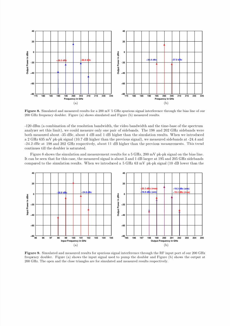
results for which spurious sideband levels at the output were about -35 dBc.Figure 9 shows the results of the simulations and measurements for spurious signal interference through the
RF input port of the frequency multiplier. Figure 9(a) shows the input signal at 100 GHz with sidebands at±1 GHz and at ±2 GHz, which is used to pump the balanced doubler. Figure 9(b) shows the simulated andmeasured results at the doubler output. Open triangles show simulated results and the close triangles measuredresults. When we introduced 10 dB lower sidebands at the input of the multiplier than the previous case (-38.8and -34.8 dBc at 99 and 101 GHz respectively, and keeping the 100 GHz signal level the same), the outputsidebands measured were at -30.2 and -29.2 dBc at 199 and 201 GHz respectively, which are about 10 dB lowerthan the previous measurements.
Here again we tried different sideband levels at the input to pump the doubler, but we plotted only thoseresults for which the first sidebands at the output are about -20 dBc. It can be seen that although the inputhad sidebands at ±1 GHz and at ±2 GHz at 100 GHz, the doubler output produced sidebands ±1 GHz and
at±
2 GHz at 200 GHz, because of the different mixing and inter-modulation products generated through thenonlinear doubler.
5. CONCLUSIONS
When a frequency multiplier experiences spurious signal interference, either through the bias line or throughthe RF input port of the multiplier, the signal is subjected to an input and output filter with symmetric diodes(because the multipliers are balanced) performing mixing of the signal with the input pump power and withthe spurious signal itself. The conversion of the sidebands in a balanced varactor diode multiplier is highlydependent on the circuit design. Because of the inherent symmetry of the balanced doubler, the odd harmonicproducts are suppressed, depending on the degree of balance in the circuit.
We observed from the simulations and the measurements that when the spurious signal levels on the bias lineof the multiplier are increased or decreased by about 10 dB, the sidebands at the output of the 200 GHz doublerincreases or decreases by the same amount, till the doubler reaches saturation. We also noticed that a signalaround 200 mV (pk-pk) in the 1–5 GHz range produces highest level sidebands in the -35 dBc level. We shouldremember that as these sidebands propagate through the multiplier chain, they will produce more sidebands,but will be at a lower level than the closest sidebands. However, other multipliers in the chain will produce theirown sidebands due to spurious signal interference through their bias lines. To reduce these sideband levels, oneneeds to look in the bias filtering of the multiplier very closely. Incorporating bandstop filters in the bias lineof the frequency multiplier in the IF frequency band will certainly help alleviate this problem.
As for the spurious signal interference through the RF input port, the sideband levels change linearly withthe input sideband level changes; when we decreased the input sideband levels by 10 dB, the output sidebandlevels also decreased by 10 dB. The spurious signal interference through the RF input port shows up slightlydifferently at the frequency multiplier output than the spurious signal interference through the bias line of themultiplier. We observed that sideband signals at ±1 GHz of the 100 GHz input signal at -25 dBc level produces
sidebands at ±1 GHz of the 200 GHz output signal at -20 dBc, a 5 dB increase in the sideband levels from theinput to the output. However, we should keep in mind that these signal levels are very much dependent onthe exact circuits used for the frequency multiplier. To reduce the spurious signal interference through the RFinput port of the multiplier, one has to pay attention to the filters used on the bias line of the millimeter wavepower amplifier modules. Overall, the simulations and the measurements showed that the multiplier did notdegrade the spurious signal interference of the LO as the spurious signals propagated through it.
In future, we are planning to run further tests and simulations by cascading more multipliers to the chain. Wealso want to study the spurious signal interference through the gate bias of the power amplifiers and its effects
8/7/2019 Frequency multiplier response to spurious signals
http://slidepdf.com/reader/full/frequency-multiplier-response-to-spurious-signals 9/9
on the frequency multiplier and the LO chain. Since the power amplifier modules are operated in saturation, thespurious signal interference through the drain bias of the power amplifier will not affect its spurious performance.We are also planning to run simulations and carry out tests with spurious signal frequencies higher than 5 GHzon the bias lines.
ACKNOWLEDGMENTS
The authors would like to thank Peter Siegel of JPL and J. Zmuidzinas of Caltech for their support. This workwas carried out at the Jet Propulsion Laboratory, California Institute of Technology, Pasadena, California, USA,under contract with National Aeronautics and Space Administration.
REFERENCES
1. N. Erickson, “Submillimeter-wave multiplier development,” To appear in the Proceedings of the Ninth International Conference on Terahertz Electronics, Charlottesville, Virginia, USA, October 15–16 2001.
2. I. Mehdi, E. Schlecht, G. Chattopadhyay, S. Martin, A. Maestrini, F. Maiwald, J. Bruston, L. Samoska, andD. Pukala, “GaAs based terahertz sources for space applications: challenges and prospects”, Proceedings of
SPIE: 45th Annual Meeting on Terahertz and Gigahertz Electronics and Photonics, vol. 4013, San Diego,California, USA, August 2000.
3. L. Samoska et al., “MMIC power amplifiers as local oscillator drivers for FIRST”, Proceedings of SPIE:
45th Annual Meeting on Terahertz and Gigahertz Electronics and Photonics, vol. 4013, pp. 275–284, SanDiego, California, USA, August 2000.
4. I. Mehdi, E. Schlecht, G. Chattopadhyay, P. H. Siegel, “THz local oscillator sources: performance andcapabilities”, Proceedings of SPIE, vol. 4855, Kona, Hawaii, USA, August 2002.
5. E. Schlecht, G. Chattopadhyay, A. Maestrini, A. Fung, S. Martin, D. Pukala, J. Bruston, and I. Mehdi,“200, 400 and 800 GHz Schottky diode substrateless multipliers: design and results”, 2001 IEEE MTT-S
International Microwave Symposium Digest , Phoenix, Arizona, USA, pp. 1649–1652, May 2001.6. S. Martin, B. Nakamura, A. Fung, P. Smith, J. Bruston, A. Maestrini, F. Maiwald, P. Siegel, E. Schlecht,
and I. Mehdi, “Fabrication of 200 to 2700 GHz multiplier devices using GaAs and metal membranes,” 2001
IEEE MTT-S International Microwave Symposium Digest , Phoenix, Arizona, USA, pp. 1641–1644, May2001.
7. G. Chattopadhyay, E. Schlecht, J. Gill, S. Martin, A. Maestrini, D. Pukala, F. Maiwald, and I. Mehdi, “Abroadband 800 GHz Schottky balanced doubler”, IEEE Microwave and Wireless Components Letters, vol.12, no. 4, pp. 117–118, April 2002.
8. E. W. Bryerton, D. L. Thacker, K. S. Saini, and R. F. Bradley, “Noise measurements of YIG-tuned oscillatorsources for the ALMA LO”, ALMA Memo No. 311, NRAO, Charlottesville, Virginia, USA, August 2000.
9. R. Ambrosini, “Measurements of Allan variance and short term phase noise of millimeter local oscillators”,ALMA Memo No. 310, NRAO, May 2000.
10. D. L. Thacker, E. W. Bryerton, R. F. Bradley, and K. S. Saini, “Phase drift measurements of YIG-tunedoscillator sources for the ALMA LO”, ALMA Memo No. 311, NRAO, Charlottesville, Virginia, USA, June2001.
11. J. W. Kooi, G. Chattopadhyay, M. Thielman, T. G. Phillips, and R. Schieder, “Noise stability of SISreceivers”, International Journal of Infrared and Millimeter Waves, vol. 21, no. 5, pp. 689–716, May 2000.
12. M. T. Faber, J. Chramiec, and M. E. Adamski, Microwave and millimeter-wave diode frequency multipliers,
Artech House, Norwood, Mass., 1995.13. Advanced Design System (ADS), version 1.5, Agilent Technologies, 395 Page Mill Road, Palo Alto, CA
94304, USA.14. High Frequency Structure Simulator (HFSS), version 8, Ansoft Corporation, Four Square Station, Suite
200, Pittsburgh, PA 15219, USA.15. N. R. Erickson, “A Fast and Sensitive Submillimeter Waveguide Power Meter”, Tenth International Space
Terahertz Technology Symposium , University of Virginia, Charlottesville, Virginia, USA, pp. 501–507,March 1999.