Technical Summary - Welcome to Freescale - Freescale Semiconductor
Freescale Semiconductor Inc.Data Sheet: Technical Data
Document Number: IMX6DQAECRev. 4, 07/2015
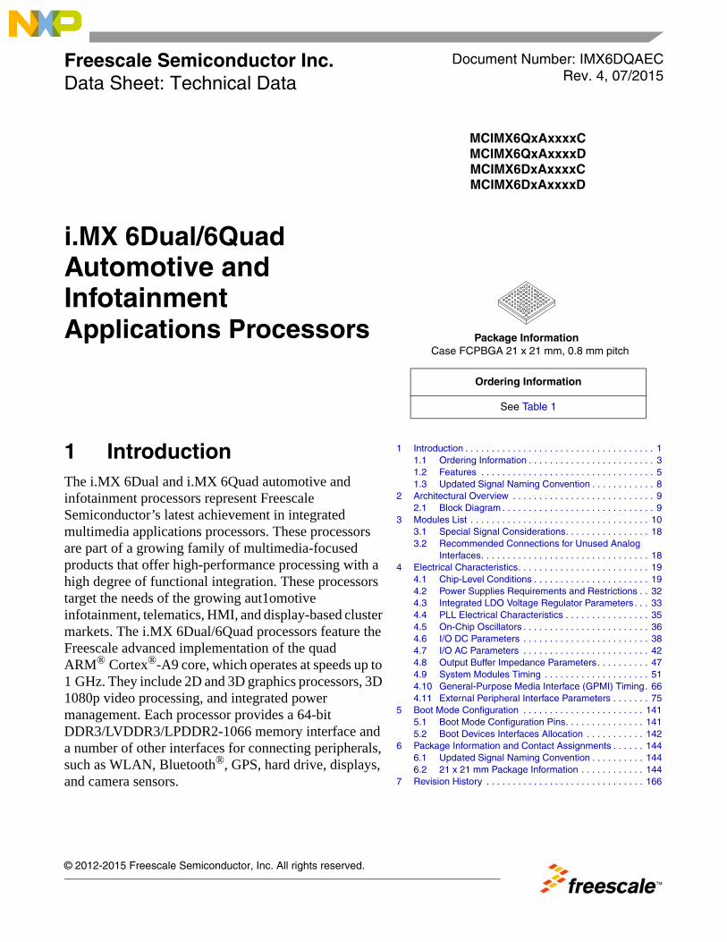
Package InformationCase FCPBGA 21 x 21 mm, 0.8 mm pitch
Ordering Information
See Table 1
© 2012-2015 Freescale Semiconductor, Inc. All rights reserved.
MCIMX6QxAxxxxCMCIMX6QxAxxxxDMCIMX6DxAxxxxCMCIMX6DxAxxxxD
1 IntroductionThe i.MX 6Dual and i.MX 6Quad automotive and infotainment processors represent Freescale Semiconductor’s latest achievement in integrated multimedia applications processors. These processors are part of a growing family of multimedia-focused products that offer high-performance processing with a high degree of functional integration. These processors target the needs of the growing aut1omotive infotainment, telematics, HMI, and display-based cluster markets. The i.MX 6Dual/6Quad processors feature the Freescale advanced implementation of the quad ARM® Cortex®-A9 core, which operates at speeds up to 1 GHz. They include 2D and 3D graphics processors, 3D 1080p video processing, and integrated power management. Each processor provides a 64-bit DDR3/LVDDR3/LPDDR2-1066 memory interface and a number of other interfaces for connecting peripherals, such as WLAN, Bluetooth®, GPS, hard drive, displays, and camera sensors.
i.MX 6Dual/6Quad Automotive and Infotainment Applications Processors
1 Introduction . . . . . . . . . . . . . . . . . . . . . . . . . . . . . . . . . . . . 11.1 Ordering Information . . . . . . . . . . . . . . . . . . . . . . . . 31.2 Features . . . . . . . . . . . . . . . . . . . . . . . . . . . . . . . . . 51.3 Updated Signal Naming Convention . . . . . . . . . . . . 8
2 Architectural Overview . . . . . . . . . . . . . . . . . . . . . . . . . . . 92.1 Block Diagram . . . . . . . . . . . . . . . . . . . . . . . . . . . . . 9
3 Modules List . . . . . . . . . . . . . . . . . . . . . . . . . . . . . . . . . . 103.1 Special Signal Considerations. . . . . . . . . . . . . . . . 183.2 Recommended Connections for Unused Analog
Interfaces. . . . . . . . . . . . . . . . . . . . . . . . . . . . . . . . 184 Electrical Characteristics. . . . . . . . . . . . . . . . . . . . . . . . . 19
4.1 Chip-Level Conditions . . . . . . . . . . . . . . . . . . . . . . 194.2 Power Supplies Requirements and Restrictions . . 324.3 Integrated LDO Voltage Regulator Parameters. . . 334.4 PLL Electrical Characteristics . . . . . . . . . . . . . . . . 354.5 On-Chip Oscillators . . . . . . . . . . . . . . . . . . . . . . . . 364.6 I/O DC Parameters . . . . . . . . . . . . . . . . . . . . . . . . 384.7 I/O AC Parameters . . . . . . . . . . . . . . . . . . . . . . . . 424.8 Output Buffer Impedance Parameters. . . . . . . . . . 474.9 System Modules Timing . . . . . . . . . . . . . . . . . . . . 514.10 General-Purpose Media Interface (GPMI) Timing. 664.11 External Peripheral Interface Parameters . . . . . . . 75
5 Boot Mode Configuration . . . . . . . . . . . . . . . . . . . . . . . 1415.1 Boot Mode Configuration Pins. . . . . . . . . . . . . . . 1415.2 Boot Devices Interfaces Allocation . . . . . . . . . . . 142
6 Package Information and Contact Assignments . . . . . . 1446.1 Updated Signal Naming Convention . . . . . . . . . . 1446.2 21 x 21 mm Package Information . . . . . . . . . . . . 144
7 Revision History . . . . . . . . . . . . . . . . . . . . . . . . . . . . . . 166
i.MX 6Dual/6Quad Automotive and Infotainment Applications Processors, Rev. 4, 07/2015
2 Freescale Semiconductor Inc.
Introduction
The i.MX 6Dual/6Quad processors are specifically useful for applications such as the following:
• Automotive navigation and entertainment
• Graphics rendering for Human Machine Interfaces (HMI)
• High-performance speech processing with large databases
• Audio playback
The i.MX 6Dual/6Quad processors offers numerous advanced features, such as:
• Multilevel memory system—The multilevel memory system of each processor is based on the L1 instruction and data caches, L2 cache, and internal and external memory. The processors support many types of external memory devices, including DDR3, low voltage DDR3, LPDDR2, NOR Flash, PSRAM, cellular RAM, NAND Flash (MLC and SLC), OneNAND™, and managed NAND, including eMMC up to rev 4.4/4.41.
• Smart speed technology—The processors have power management throughout the device that enables the rich suite of multimedia features and peripherals to consume minimum power in both active and various low power modes. Smart speed technology enables the designer to deliver a feature-rich product, requiring levels of power far lower than industry expectations.
• Dynamic voltage and frequency scaling—The processors improve the power efficiency of devices by scaling the voltage and frequency to optimize performance.
• Multimedia powerhouse—The multimedia performance of each processor is enhanced by a multilevel cache system, Neon® MPE (Media Processor Engine) co-processor, a multi-standard hardware video codec, 2 autonomous and independent image processing units (IPU), and a programmable smart DMA (SDMA) controller.
• Powerful graphics acceleration—Each processor provides three independent, integrated graphics processing units: an OpenGL® ES 2.0 3D graphics accelerator with four shaders (up to 200 MTri/s and OpenCL support), 2D graphics accelerator, and dedicated OpenVG™ 1.1 accelerator.
• Interface flexibility—Each processor supports connections to a variety of interfaces: LCD controller for up to four displays (including parallel display, HDMI1.4, MIPI display, and LVDS display), dual CMOS sensor interface (parallel or through MIPI), high-speed USB on-the-go with PHY, high-speed USB host with PHY, multiple expansion card ports (high-speed MMC/SDIO host and other), 10/100/1000 Mbps Gigabit Ethernet controller, and a variety of other popular interfaces (such as UART, I2C, and I2S serial audio, SATA-II, and PCIe-II).
• Automotive environment support—Each processor includes interfaces, such as two CAN ports, an MLB150/50 port, an ESAI audio interface, and an asynchronous sample rate converter for multichannel/multisource audio.
• Advanced security—The processors deliver hardware-enabled security features that enable secure e-commerce, digital rights management (DRM), information encryption, secure boot, and secure software downloads. The security features are discussed in detail in the i.MX 6Dual/6Quad security reference manual (IMX6DQ6SDLSRM).
• Integrated power management—The processors integrate linear regulators and internally generate voltage levels for different domains. This significantly simplifies system power management structure.
Introduction
i.MX 6Dual/6Quad Automotive and Infotainment Applications Processors, Rev. 4, 07/2015
Freescale Semiconductor Inc. 3
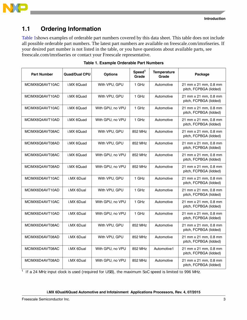
1.1 Ordering InformationTable 1shows examples of orderable part numbers covered by this data sheet. This table does not include all possible orderable part numbers. The latest part numbers are available on freescale.com/imx6series. If your desired part number is not listed in the table, or you have questions about available parts, see freescale.com/imx6series or contact your Freescale representative.
Table 1. Example Orderable Part Numbers
Part Number Quad/Dual CPU OptionsSpeed1 Grade
1 If a 24 MHz input clock is used (required for USB), the maximum SoC speed is limited to 996 MHz.
Temperature Grade
Package
MCIMX6Q6AVT10AC i.MX 6Quad With VPU, GPU 1 GHz Automotive 21 mm x 21 mm, 0.8 mm pitch, FCPBGA (lidded)
MCIMX6Q6AVT10AD i.MX 6Quad With VPU, GPU 1 GHz Automotive 21 mm x 21 mm, 0.8 mm pitch, FCPBGA (lidded)
MCIMX6Q4AVT10AC i.MX 6Quad With GPU, no VPU 1 GHz Automotive 21 mm x 21 mm, 0.8 mm pitch, FCPBGA (lidded)
MCIMX6Q4AVT10AD i.MX 6Quad With GPU, no VPU 1 GHz Automotive 21 mm x 21 mm, 0.8 mm pitch, FCPBGA (lidded)
MCIMX6Q6AVT08AC i.MX 6Quad With VPU, GPU 852 MHz Automotive 21 mm x 21 mm, 0.8 mm pitch, FCPBGA (lidded)
MCIMX6Q6AVT08AD i.MX 6Quad With VPU, GPU 852 MHz Automotive 21 mm x 21 mm, 0.8 mm pitch, FCPBGA (lidded)
MCIMX6Q4AVT08AC i.MX 6Quad With GPU, no VPU 852 MHz Automotive 21 mm x 21 mm, 0.8 mm pitch, FCPBGA (lidded)
MCIMX6Q4AVT08AD i.MX 6Quad With GPU, no VPU 852 MHz Automotive 21 mm x 21 mm, 0.8 mm pitch, FCPBGA (lidded)
MCIMX6D6AVT10AC i.MX 6Dual With VPU, GPU 1 GHz Automotive 21 mm x 21 mm, 0.8 mm pitch, FCPBGA (lidded)
MCIMX6D6AVT10AD i.MX 6Dual With VPU, GPU 1 GHz Automotive 21 mm x 21 mm, 0.8 mm pitch, FCPBGA (lidded)
MCIMX6D4AVT10AC i.MX 6Dual With GPU, no VPU 1 GHz Automotive 21 mm x 21 mm, 0.8 mm pitch, FCPBGA (lidded)
MCIMX6D4AVT10AD i.MX 6Dual With GPU, no VPU 1 GHz Automotive 21 mm x 21 mm, 0.8 mm pitch, FCPBGA (lidded)
MCIMX6D6AVT08AC i.MX 6Dual With VPU, GPU 852 MHz Automotive 21 mm x 21 mm, 0.8 mm pitch, FCPBGA (lidded)
MCIMX6D6AVT08AD i.MX 6Dual With VPU, GPU 852 MHz Automotive 21 mm x 21 mm, 0.8 mm pitch, FCPBGA (lidded)
MCIMX6D4AVT08AC i.MX 6Dual With GPU, no VPU 852 MHz Automotive1 21 mm x 21 mm, 0.8 mm pitch, FCPBGA (lidded)
MCIMX6D4AVT08AD i.MX 6Dual With GPU, no VPU 852 MHz Automotive 21 mm x 21 mm, 0.8 mm pitch, FCPBGA (lidded)
i.MX 6Dual/6Quad Automotive and Infotainment Applications Processors, Rev. 4, 07/2015
4 Freescale Semiconductor Inc.
Introduction
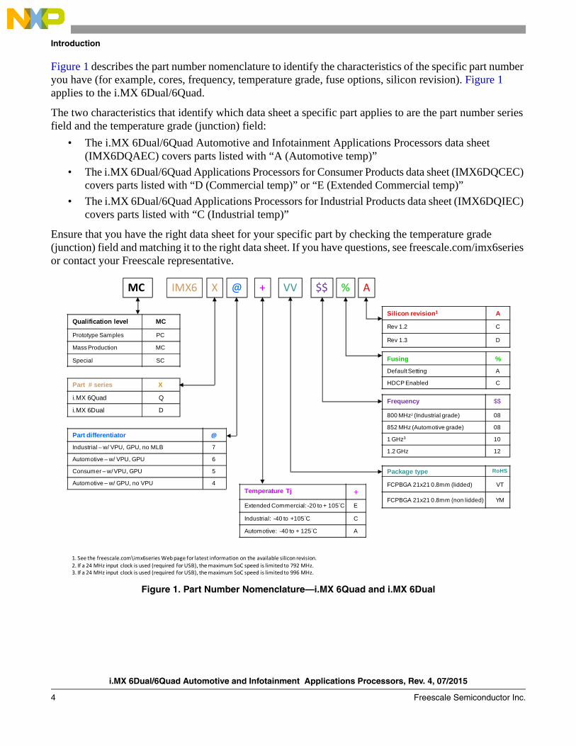
Figure 1 describes the part number nomenclature to identify the characteristics of the specific part number you have (for example, cores, frequency, temperature grade, fuse options, silicon revision). Figure 1 applies to the i.MX 6Dual/6Quad.
The two characteristics that identify which data sheet a specific part applies to are the part number series field and the temperature grade (junction) field:
• The i.MX 6Dual/6Quad Automotive and Infotainment Applications Processors data sheet (IMX6DQAEC) covers parts listed with “A (Automotive temp)”
• The i.MX 6Dual/6Quad Applications Processors for Consumer Products data sheet (IMX6DQCEC) covers parts listed with “D (Commercial temp)” or “E (Extended Commercial temp)”
• The i.MX 6Dual/6Quad Applications Processors for Industrial Products data sheet (IMX6DQIEC) covers parts listed with “C (Industrial temp)”
Ensure that you have the right data sheet for your specific part by checking the temperature grade (junction) field and matching it to the right data sheet. If you have questions, see freescale.com/imx6series or contact your Freescale representative.
Figure 1. Part Number Nomenclature—i.MX 6Quad and i.MX 6Dual
Part differentiator @
Industrial – w/ VPU, GPU, no MLB 7
Automotive – w/ VPU, GPU 6
Consumer – w/ VPU, GPU 5
Automotive – w/ GPU, no VPU 4Temperature Tj +
Extended Commercial: -20 to + 105°C E
Industrial: -40 to +105°C C
Automotive: -40 to + 125°C A
Frequency $$
800 MHz2 (Industrial grade) 08
852 MHz (Automotive grade) 08
1 GHz3 10
1.2 GHz 12
Package type RoHS
FCPBGA 21x21 0.8mm (lidded) VT
FCPBGA 21x21 0.8mm (non lidded) YM
Qualification level MC
Prototype Samples PC
Mass Production MC
Special SC
Part # series X
i.MX 6Quad Q
i.MX 6Dual D
Silicon revision1 A
Rev 1.2 C
Rev 1.3 D
Fusing %
Default Setting A
HDCP Enabled C
MC IMX6 X @ + VV $$ % A
1. See the freescale.com\imx6series Web page for latest information on the available silicon revision.2. If a 24 MHz input clock is used (required for USB), the maximum SoC speed is limited to 792 MHz.3. If a 24 MHz input clock is used (required for USB), the maximum SoC speed is limited to 996 MHz.
Introduction
i.MX 6Dual/6Quad Automotive and Infotainment Applications Processors, Rev. 4, 07/2015
Freescale Semiconductor Inc. 5
1.2 FeaturesThe i.MX 6Dual/6Quad processors are based on ARM Cortex-A9 MPCore platform, which has the following features:
• ARM Cortex-A9 MPCore 4xCPU processor (with TrustZone®)• The core configuration is symmetric, where each core includes:
— 32 KByte L1 Instruction Cache
— 32 KByte L1 Data Cache
— Private Timer and Watchdog
— Cortex-A9 NEON MPE (Media Processing Engine) Co-processor
The ARM Cortex-A9 MPCore complex includes:
• General Interrupt Controller (GIC) with 128 interrupt support
• Global Timer
• Snoop Control Unit (SCU)
• 1 MB unified I/D L2 cache, shared by two/four cores
• Two Master AXI (64-bit) bus interfaces output of L2 cache
• Frequency of the core (including Neon and L1 cache) as per Table 6.
• NEON MPE coprocessor
— SIMD Media Processing Architecture
— NEON register file with 32x64-bit general-purpose registers
— NEON Integer execute pipeline (ALU, Shift, MAC)
— NEON dual, single-precision floating point execute pipeline (FADD, FMUL)
— NEON load/store and permute pipeline
The SoC-level memory system consists of the following additional components:
— Boot ROM, including HAB (96 KB)
— Internal multimedia / shared, fast access RAM (OCRAM, 256 KB)
— Secure/non-secure RAM (16 KB)
• External memory interfaces:
— 16-bit, 32-bit, and 64-bit DDR3-1066, LVDDR3-1066, and 1/2 LPDDR2-1066 channels, supporting DDR interleaving mode, for 2x32 LPDDR2-1066
— 8-bit NAND-Flash, including support for Raw MLC/SLC, 2 KB, 4 KB, and 8 KB page size, BA-NAND, PBA-NAND, LBA-NAND, OneNAND™ and others. BCH ECC up to 40 bit.
— 16/32-bit NOR Flash. All EIMv2 pins are muxed on other interfaces.
— 16/32-bit PSRAM, Cellular RAM
Each i.MX 6Dual/6Quad processor enables the following interfaces to external devices (some of them are muxed and not available simultaneously):
• Hard Disk Drives—SATA II, 3.0 Gbps
i.MX 6Dual/6Quad Automotive and Infotainment Applications Processors, Rev. 4, 07/2015
6 Freescale Semiconductor Inc.
Introduction
• Displays—Total five interfaces available. Total raw pixel rate of all interfaces is up to 450 Mpixels/sec, 24 bpp. Up to four interfaces may be active in parallel.
— One Parallel 24-bit display port, up to 225 Mpixels/sec (for example, WUXGA at 60 Hz or dual HD1080 and WXGA at 60 Hz)
— LVDS serial ports—One port up to 165 Mpixels/sec or two ports up to 85 MP/sec (for example, WUXGA at 60 Hz) each
— HDMI 1.4 port
— MIPI/DSI, two lanes at 1 Gbps
• Camera sensors:
— Parallel Camera port (up to 20 bit and up to 240 MHz peak)
— MIPI CSI-2 serial camera port, supporting up to 1000 Mbps/lane in 1/2/3-lane mode and up to 800 Mbps/lane in 4-lane mode. The CSI-2 Receiver core can manage one clock lane and up to four data lanes. Each i.MX 6Dual/6Quad processor has four lanes.
• Expansion cards:
— Four MMC/SD/SDIO card ports all supporting:
– 1-bit or 4-bit transfer mode specifications for SD and SDIO cards up to UHS-I SDR-104 mode (104 MB/s max)
– 1-bit, 4-bit, or 8-bit transfer mode specifications for MMC cards up to 52 MHz in both SDR and DDR modes (104 MB/s max)
• USB:
— One High Speed (HS) USB 2.0 OTG (Up to 480 Mbps), with integrated HS USB PHY
— Three USB 2.0 (480 Mbps) hosts:
– One HS host with integrated High Speed PHY
– Two HS hosts with integrated HS-IC USB (High Speed Inter-Chip USB) PHY
• Expansion PCI Express port (PCIe) v2.0 one lane
— PCI Express (Gen 2.0) dual mode complex, supporting Root complex operations and Endpoint operations. Uses x1 PHY configuration.
• Miscellaneous IPs and interfaces:
— SSI block capable of supporting audio sample frequencies up to 192 kHz stereo inputs and outputs with I2S mode
— ESAI is capable of supporting audio sample frequencies up to 260kHz in I2S mode with 7.1 multi channel outputs
— Five UARTs, up to 5.0 Mbps each:
– Providing RS232 interface
– Supporting 9-bit RS485 multidrop mode
– One of the five UARTs (UART1) supports 8-wire while others four supports 4-wire. This is due to the SoC IOMUX limitation, since all UART IPs are identical.
— Five eCSPI (Enhanced CSPI)
— Three I2C, supporting 400 kbps
Introduction
i.MX 6Dual/6Quad Automotive and Infotainment Applications Processors, Rev. 4, 07/2015
Freescale Semiconductor Inc. 7
— Gigabit Ethernet Controller (IEEE1588 compliant), 10/100/10001 Mbps
— Four Pulse Width Modulators (PWM)
— System JTAG Controller (SJC)
— GPIO with interrupt capabilities
— 8x8 Key Pad Port (KPP)
— Sony Philips Digital Interconnect Format (SPDIF), Rx and Tx
— Two Controller Area Network (FlexCAN), 1 Mbps each
— Two Watchdog timers (WDOG)
— Audio MUX (AUDMUX)
— MLB (MediaLB) provides interface to MOST Networks (150 Mbps) with the option of DTCP cipher accelerator
The i.MX 6Dual/6Quad processors integrate advanced power management unit and controllers:
• Provide PMU, including LDO supplies, for on-chip resources
• Use Temperature Sensor for monitoring the die temperature
• Support DVFS techniques for low power modes
• Use Software State Retention and Power Gating for ARM and MPE
• Support various levels of system power modes
• Use flexible clock gating control scheme
The i.MX 6Dual/6Quad processors use dedicated hardware accelerators to meet the targeted multimedia performance. The use of hardware accelerators is a key factor in obtaining high performance at low power consumption numbers, while having the CPU core relatively free for performing other tasks.
The i.MX 6Dual/6Quad processors incorporate the following hardware accelerators:
• VPU—Video Processing Unit
• IPUv3H—Image Processing Unit version 3H (2 IPUs)
• GPU3Dv4—3D Graphics Processing Unit (OpenGL ES 2.0) version 4
• GPU2Dv2—2D Graphics Processing Unit (BitBlt)
• GPUVG—OpenVG 1.1 Graphics Processing Unit
• ASRC—Asynchronous Sample Rate Converter
Security functions are enabled and accelerated by the following hardware:
• ARM TrustZone including the TZ architecture (separation of interrupts, memory mapping, etc.)
• SJC—System JTAG Controller. Protecting JTAG from debug port attacks by regulating or blocking the access to the system debug features.
• CAAM—Cryptographic Acceleration and Assurance Module, containing 16 KB secure RAM and True and Pseudo Random Number Generator (NIST certified)
• SNVS—Secure Non-Volatile Storage, including Secure Real Time Clock
1. The theoretical maximum performance of 1 Gbps ENET is limited to 470 Mbps (total for Tx and Rx) due to internal bus throughput limitations. The actual measured performance in optimized environment is up to 400 Mbps. For details, see the ERR004512 erratum in the i.MX 6Dual/6Quad errata document (IMX6DQCE).
i.MX 6Dual/6Quad Automotive and Infotainment Applications Processors, Rev. 4, 07/2015
8 Freescale Semiconductor Inc.
Introduction
• CSU—Central Security Unit. Enhancement for the IC Identification Module (IIM). Will be configured during boot and by eFUSEs and will determine the security level operation mode as well as the TZ policy.
• A-HAB—Advanced High Assurance Boot—HABv4 with the new embedded enhancements: SHA-256, 2048-bit RSA key, version control mechanism, warm boot, CSU, and TZ initialization.
1.3 Updated Signal Naming ConventionThe signal names of the i.MX 6 series of products have been standardized to better align the signal names within the family and across the documentation. Some of the benefits of these changes are as follows:
• The names are unique within the scope of an SoC and within the series of products
• Searches will return all occurrences of the named signal
• The names are consistent between i.MX 6 series products implementing the same modules
• The module instance is incorporated into the signal name
This change applies only to signal names. The original ball names have been preserved to prevent the need to change schematics, BSDL models, IBIS models, etc.
Throughout this document, the updated signal names are used except where referenced as a ball name (such as the Functional Contact Assignments table, Ball Map table, and so on). A master list of the signal name changes is in the document, IMX 6 Series Signal Name Mapping (EB792). This list can be used to map the signal names used in older documentation to the new standardized naming conventions.
Architectural Overview
i.MX 6Dual/6Quad Automotive and Infotainment Applications Processors, Rev. 4, 07/2015
Freescale Semiconductor Inc. 9
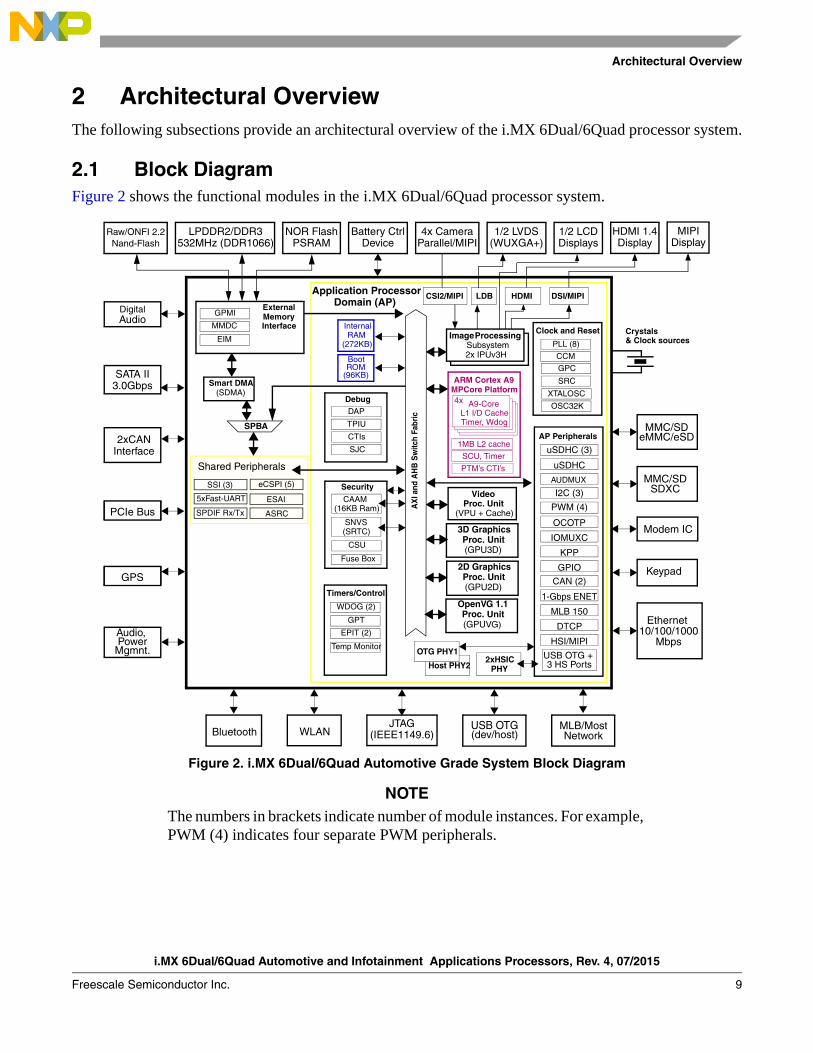
2 Architectural OverviewThe following subsections provide an architectural overview of the i.MX 6Dual/6Quad processor system.
2.1 Block DiagramFigure 2 shows the functional modules in the i.MX 6Dual/6Quad processor system.
Figure 2. i.MX 6Dual/6Quad Automotive Grade System Block Diagram
NOTEThe numbers in brackets indicate number of module instances. For example, PWM (4) indicates four separate PWM peripherals.
Smart DMA(SDMA)
Shared Peripherals
AP Peripherals
ARM Cortex A9
SSI (3) eCSPI (5)
MPCore Platform
Timers/Control
GPT
PWM (4)
EPIT (2)
GPIO
WDOG (2)
I2C (3)
IOMUXC
OCOTP
AUDMUX
KPP
BootROM
CSU
Fuse Box
DebugDAP
TPIU
CAAM(16KB Ram)
Security
USB OTG + 3 HS Ports
CTIs
Internal
Host PHY2
OTG PHY1
ESAI
ExternalMemory
RAM(272KB)
LDB
1/2 LCDDisplays
Domain (AP)
SJC1MB L2 cache
SCU, Timer
WLANUSB OTGJTAG
(IEEE1149.6)Bluetooth
MMC/SDeMMC/eSD
SATA II3.0Gbps
GPS
Audio, Power
Mgmnt.
SPBA
CAN (2)
DigitalAudio
5xFast-UART
SPDIF Rx/Tx
VideoProc. Unit
(VPU + Cache)
3D GraphicsProc. Unit(GPU3D)
AX
I and
AH
B S
witc
h Fa
bric
1/2 LVDS(WUXGA+)
Battery CtrlDevice
NOR FlashPSRAM
LPDDR2/DDR3532MHz (DDR1066)
1-Gbps ENET
MLB 150
4x CameraParallel/MIPI
(96KB)
Clock and Reset
PLL (8)
CCM
GPC
SRC
XTALOSC
OSC32K
PTM’s CTI’s
HDMI 1.4Display
GPMI
HSI/MIPI
MIPIDisplay
DSI/MIPIHDMI
2xHSICPHY
PCIe Bus ASRCSNVS(SRTC)
uSDHC
uSDHC (3)
Modem IC
2D GraphicsProc. Unit(GPU2D)
MMC/SDSDXC
Raw/ONFI 2.2Nand-Flash
MMDC
EIM
Keypad
A9-CoreL1 I/D CacheTimer, Wdog
4x
DTCP
Crystals& Clock sourcesImageProcessing
Subsystem2x IPUv3H
Temp Monitor
MLB/Most
OpenVG 1.1Proc. Unit(GPUVG)
Mbps10/100/1000
Ethernet
Network(dev/host)
Interface
2xCAN Interface
GPSGPS
CSI2/MIPIApplication Processor
i.MX 6Dual/6Quad Automotive and Infotainment Applications Processors, Rev. 4, 07/2015
10 Freescale Semiconductor Inc.
Modules List
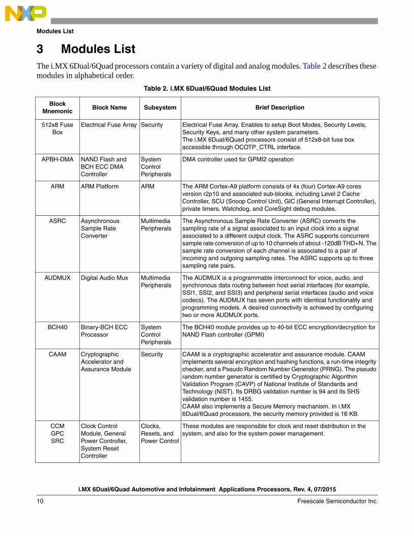
3 Modules ListThe i.MX 6Dual/6Quad processors contain a variety of digital and analog modules. Table 2 describes these modules in alphabetical order.
Table 2. i.MX 6Dual/6Quad Modules List
Block Mnemonic
Block Name Subsystem Brief Description
512x8 Fuse Box
Electrical Fuse Array Security Electrical Fuse Array. Enables to setup Boot Modes, Security Levels, Security Keys, and many other system parameters.The i.MX 6Dual/6Quad processors consist of 512x8-bit fuse box accessible through OCOTP_CTRL interface.
APBH-DMA NAND Flash and BCH ECC DMA Controller
System Control Peripherals
DMA controller used for GPMI2 operation
ARM ARM Platform ARM The ARM Cortex-A9 platform consists of 4x (four) Cortex-A9 cores version r2p10 and associated sub-blocks, including Level 2 Cache Controller, SCU (Snoop Control Unit), GIC (General Interrupt Controller), private timers, Watchdog, and CoreSight debug modules.
ASRC Asynchronous Sample Rate Converter
Multimedia Peripherals
The Asynchronous Sample Rate Converter (ASRC) converts the sampling rate of a signal associated to an input clock into a signal associated to a different output clock. The ASRC supports concurrent sample rate conversion of up to 10 channels of about -120dB THD+N. The sample rate conversion of each channel is associated to a pair of incoming and outgoing sampling rates. The ASRC supports up to three sampling rate pairs.
AUDMUX Digital Audio Mux Multimedia Peripherals
The AUDMUX is a programmable interconnect for voice, audio, and synchronous data routing between host serial interfaces (for example, SSI1, SSI2, and SSI3) and peripheral serial interfaces (audio and voice codecs). The AUDMUX has seven ports with identical functionality and programming models. A desired connectivity is achieved by configuring two or more AUDMUX ports.
BCH40 Binary-BCH ECC Processor
System Control Peripherals
The BCH40 module provides up to 40-bit ECC encryption/decryption for NAND Flash controller (GPMI)
CAAM Cryptographic Accelerator and Assurance Module
Security CAAM is a cryptographic accelerator and assurance module. CAAM implements several encryption and hashing functions, a run-time integrity checker, and a Pseudo Random Number Generator (PRNG). The pseudo random number generator is certified by Cryptographic Algorithm Validation Program (CAVP) of National Institute of Standards and Technology (NIST). Its DRBG validation number is 94 and its SHS validation number is 1455.CAAM also implements a Secure Memory mechanism. In i.MX 6Dual/6Quad processors, the security memory provided is 16 KB.
CCMGPCSRC
Clock Control Module, General Power Controller, System Reset Controller
Clocks, Resets, and Power Control
These modules are responsible for clock and reset distribution in the system, and also for the system power management.
Modules List
i.MX 6Dual/6Quad Automotive and Infotainment Applications Processors, Rev. 4, 07/2015
Freescale Semiconductor Inc. 11
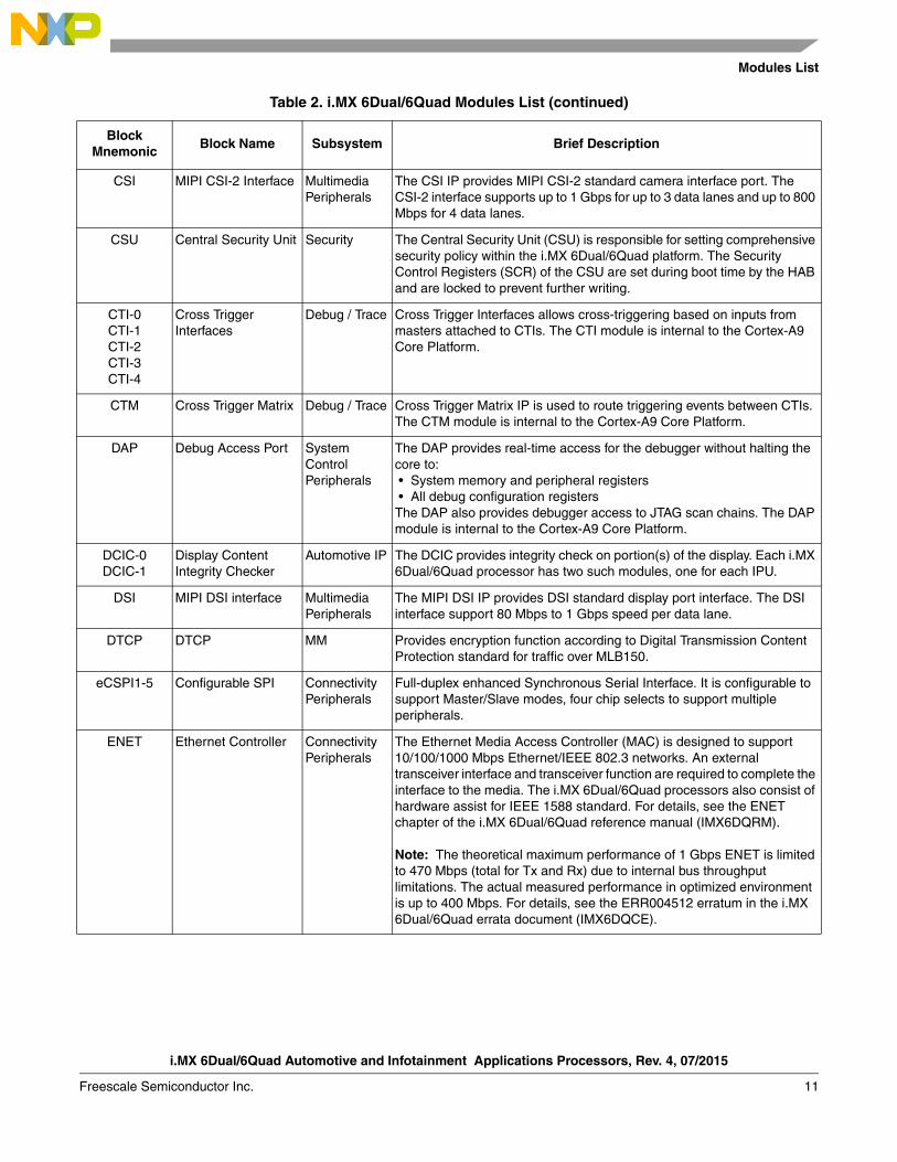
CSI MIPI CSI-2 Interface Multimedia Peripherals
The CSI IP provides MIPI CSI-2 standard camera interface port. The CSI-2 interface supports up to 1 Gbps for up to 3 data lanes and up to 800 Mbps for 4 data lanes.
CSU Central Security Unit Security The Central Security Unit (CSU) is responsible for setting comprehensive security policy within the i.MX 6Dual/6Quad platform. The Security Control Registers (SCR) of the CSU are set during boot time by the HAB and are locked to prevent further writing.
CTI-0CTI-1CTI-2CTI-3CTI-4
Cross Trigger Interfaces
Debug / Trace Cross Trigger Interfaces allows cross-triggering based on inputs from masters attached to CTIs. The CTI module is internal to the Cortex-A9 Core Platform.
CTM Cross Trigger Matrix Debug / Trace Cross Trigger Matrix IP is used to route triggering events between CTIs. The CTM module is internal to the Cortex-A9 Core Platform.
DAP Debug Access Port System Control Peripherals
The DAP provides real-time access for the debugger without halting the core to: • System memory and peripheral registers • All debug configuration registersThe DAP also provides debugger access to JTAG scan chains. The DAP module is internal to the Cortex-A9 Core Platform.
DCIC-0DCIC-1
Display Content Integrity Checker
Automotive IP The DCIC provides integrity check on portion(s) of the display. Each i.MX 6Dual/6Quad processor has two such modules, one for each IPU.
DSI MIPI DSI interface Multimedia Peripherals
The MIPI DSI IP provides DSI standard display port interface. The DSI interface support 80 Mbps to 1 Gbps speed per data lane.
DTCP DTCP MM Provides encryption function according to Digital Transmission Content Protection standard for traffic over MLB150.
eCSPI1-5 Configurable SPI Connectivity Peripherals
Full-duplex enhanced Synchronous Serial Interface. It is configurable to support Master/Slave modes, four chip selects to support multiple peripherals.
ENET Ethernet Controller Connectivity Peripherals
The Ethernet Media Access Controller (MAC) is designed to support 10/100/1000 Mbps Ethernet/IEEE 802.3 networks. An external transceiver interface and transceiver function are required to complete the interface to the media. The i.MX 6Dual/6Quad processors also consist of hardware assist for IEEE 1588 standard. For details, see the ENET chapter of the i.MX 6Dual/6Quad reference manual (IMX6DQRM).
Note: The theoretical maximum performance of 1 Gbps ENET is limited to 470 Mbps (total for Tx and Rx) due to internal bus throughput limitations. The actual measured performance in optimized environment is up to 400 Mbps. For details, see the ERR004512 erratum in the i.MX 6Dual/6Quad errata document (IMX6DQCE).
Table 2. i.MX 6Dual/6Quad Modules List (continued)
Block Mnemonic
Block Name Subsystem Brief Description
i.MX 6Dual/6Quad Automotive and Infotainment Applications Processors, Rev. 4, 07/2015
12 Freescale Semiconductor Inc.
Modules List
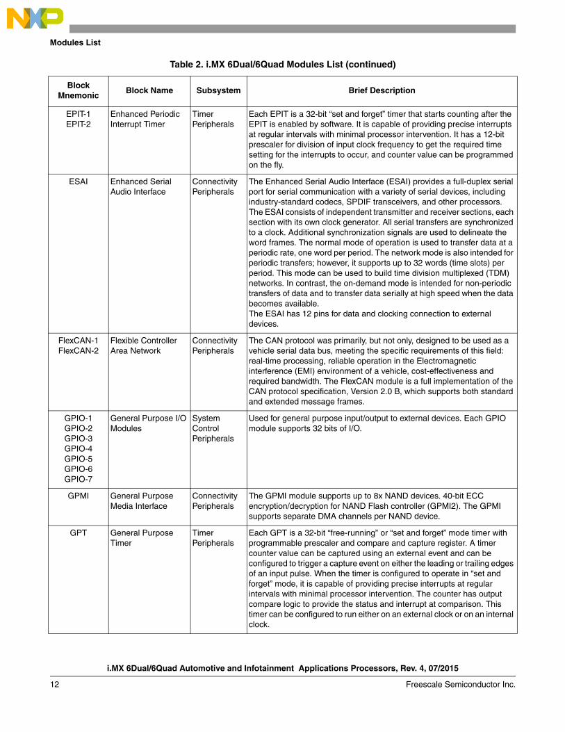
EPIT-1EPIT-2
Enhanced Periodic Interrupt Timer
Timer Peripherals
Each EPIT is a 32-bit “set and forget” timer that starts counting after the EPIT is enabled by software. It is capable of providing precise interrupts at regular intervals with minimal processor intervention. It has a 12-bit prescaler for division of input clock frequency to get the required time setting for the interrupts to occur, and counter value can be programmed on the fly.
ESAI Enhanced Serial Audio Interface
Connectivity Peripherals
The Enhanced Serial Audio Interface (ESAI) provides a full-duplex serial port for serial communication with a variety of serial devices, including industry-standard codecs, SPDIF transceivers, and other processors.The ESAI consists of independent transmitter and receiver sections, each section with its own clock generator. All serial transfers are synchronized to a clock. Additional synchronization signals are used to delineate the word frames. The normal mode of operation is used to transfer data at a periodic rate, one word per period. The network mode is also intended for periodic transfers; however, it supports up to 32 words (time slots) per period. This mode can be used to build time division multiplexed (TDM) networks. In contrast, the on-demand mode is intended for non-periodic transfers of data and to transfer data serially at high speed when the data becomes available.The ESAI has 12 pins for data and clocking connection to external devices.
FlexCAN-1FlexCAN-2
Flexible Controller Area Network
Connectivity Peripherals
The CAN protocol was primarily, but not only, designed to be used as a vehicle serial data bus, meeting the specific requirements of this field: real-time processing, reliable operation in the Electromagnetic interference (EMI) environment of a vehicle, cost-effectiveness and required bandwidth. The FlexCAN module is a full implementation of the CAN protocol specification, Version 2.0 B, which supports both standard and extended message frames.
GPIO-1GPIO-2GPIO-3GPIO-4GPIO-5GPIO-6GPIO-7
General Purpose I/O Modules
System Control Peripherals
Used for general purpose input/output to external devices. Each GPIO module supports 32 bits of I/O.
GPMI General Purpose Media Interface
Connectivity Peripherals
The GPMI module supports up to 8x NAND devices. 40-bit ECC encryption/decryption for NAND Flash controller (GPMI2). The GPMI supports separate DMA channels per NAND device.
GPT General Purpose Timer
Timer Peripherals
Each GPT is a 32-bit “free-running” or “set and forget” mode timer with programmable prescaler and compare and capture register. A timer counter value can be captured using an external event and can be configured to trigger a capture event on either the leading or trailing edges of an input pulse. When the timer is configured to operate in “set and forget” mode, it is capable of providing precise interrupts at regular intervals with minimal processor intervention. The counter has output compare logic to provide the status and interrupt at comparison. This timer can be configured to run either on an external clock or on an internal clock.
Table 2. i.MX 6Dual/6Quad Modules List (continued)
Block Mnemonic
Block Name Subsystem Brief Description
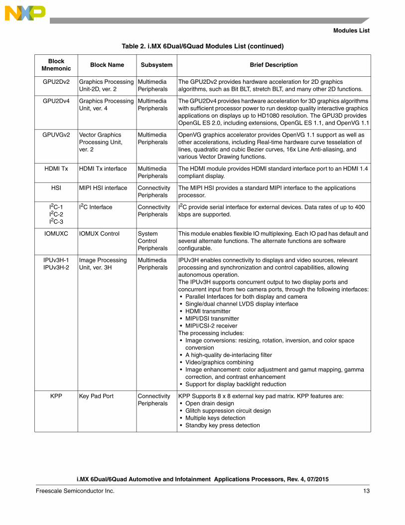
Modules List
i.MX 6Dual/6Quad Automotive and Infotainment Applications Processors, Rev. 4, 07/2015
Freescale Semiconductor Inc. 13
GPU2Dv2 Graphics Processing Unit-2D, ver. 2
Multimedia Peripherals
The GPU2Dv2 provides hardware acceleration for 2D graphics algorithms, such as Bit BLT, stretch BLT, and many other 2D functions.
GPU2Dv4 Graphics Processing Unit, ver. 4
Multimedia Peripherals
The GPU2Dv4 provides hardware acceleration for 3D graphics algorithms with sufficient processor power to run desktop quality interactive graphics applications on displays up to HD1080 resolution. The GPU3D provides OpenGL ES 2.0, including extensions, OpenGL ES 1.1, and OpenVG 1.1
GPUVGv2 Vector Graphics Processing Unit,ver. 2
Multimedia Peripherals
OpenVG graphics accelerator provides OpenVG 1.1 support as well as other accelerations, including Real-time hardware curve tesselation of lines, quadratic and cubic Bezier curves, 16x Line Anti-aliasing, and various Vector Drawing functions.
HDMI Tx HDMI Tx interface Multimedia Peripherals
The HDMI module provides HDMI standard interface port to an HDMI 1.4 compliant display.
HSI MIPI HSI interface Connectivity Peripherals
The MIPI HSI provides a standard MIPI interface to the applications processor.
I2C-1I2C-2I2C-3
I2C Interface Connectivity Peripherals
I2C provide serial interface for external devices. Data rates of up to 400 kbps are supported.
IOMUXC IOMUX Control System Control Peripherals
This module enables flexible IO multiplexing. Each IO pad has default and several alternate functions. The alternate functions are software configurable.
IPUv3H-1IPUv3H-2
Image Processing Unit, ver. 3H
Multimedia Peripherals
IPUv3H enables connectivity to displays and video sources, relevant processing and synchronization and control capabilities, allowing autonomous operation.The IPUv3H supports concurrent output to two display ports and concurrent input from two camera ports, through the following interfaces: • Parallel Interfaces for both display and camera • Single/dual channel LVDS display interface • HDMI transmitter • MIPI/DSI transmitter • MIPI/CSI-2 receiverThe processing includes: • Image conversions: resizing, rotation, inversion, and color space
conversion • A high-quality de-interlacing filter • Video/graphics combining • Image enhancement: color adjustment and gamut mapping, gamma
correction, and contrast enhancement • Support for display backlight reduction
KPP Key Pad Port Connectivity Peripherals
KPP Supports 8 x 8 external key pad matrix. KPP features are: • Open drain design • Glitch suppression circuit design • Multiple keys detection • Standby key press detection
Table 2. i.MX 6Dual/6Quad Modules List (continued)
Block Mnemonic
Block Name Subsystem Brief Description
i.MX 6Dual/6Quad Automotive and Infotainment Applications Processors, Rev. 4, 07/2015
14 Freescale Semiconductor Inc.
Modules List
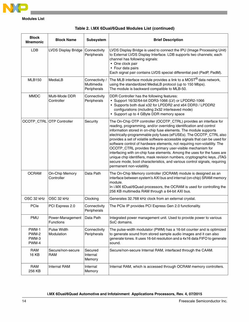
LDB LVDS Display Bridge Connectivity Peripherals
LVDS Display Bridge is used to connect the IPU (Image Processing Unit) to External LVDS Display Interface. LDB supports two channels; each channel has following signals: • One clock pair • Four data pairsEach signal pair contains LVDS special differential pad (PadP, PadM).
MLB150 MediaLB Connectivity / Multimedia Peripherals
The MLB interface module provides a link to a MOST® data network, using the standardized MediaLB protocol (up to 150 Mbps).The module is backward compatible to MLB-50.
MMDC Multi-Mode DDR Controller
Connectivity Peripherals
DDR Controller has the following features: • Support 16/32/64-bit DDR3-1066 (LV) or LPDDR2-1066 • Supports both dual x32 for LPDDR2 and x64 DDR3 / LPDDR2
configurations (including 2x32 interleaved mode) • Support up to 4 GByte DDR memory space
OCOTP_CTRL OTP Controller Security The On-Chip OTP controller (OCOTP_CTRL) provides an interface for reading, programming, and/or overriding identification and control information stored in on-chip fuse elements. The module supports electrically-programmable poly fuses (eFUSEs). The OCOTP_CTRL also provides a set of volatile software-accessible signals that can be used for software control of hardware elements, not requiring non-volatility. The OCOTP_CTRL provides the primary user-visible mechanism for interfacing with on-chip fuse elements. Among the uses for the fuses are unique chip identifiers, mask revision numbers, cryptographic keys, JTAG secure mode, boot characteristics, and various control signals, requiring permanent non-volatility.
OCRAM On-Chip Memory Controller
Data Path The On-Chip Memory controller (OCRAM) module is designed as an interface between system’s AXI bus and internal (on-chip) SRAM memory module.In i.MX 6Dual/6Quad processors, the OCRAM is used for controlling the 256 KB multimedia RAM through a 64-bit AXI bus.
OSC 32 kHz OSC 32 kHz Clocking Generates 32.768 kHz clock from an external crystal.
PCIe PCI Express 2.0 Connectivity Peripherals
The PCIe IP provides PCI Express Gen 2.0 functionality.
PMU Power-Management Functions
Data Path Integrated power management unit. Used to provide power to various SoC domains.
PWM-1PWM-2PWM-3PWM-4
Pulse Width Modulation
Connectivity Peripherals
The pulse-width modulator (PWM) has a 16-bit counter and is optimized to generate sound from stored sample audio images and it can also generate tones. It uses 16-bit resolution and a 4x16 data FIFO to generate sound.
RAM16 KB
Secure/non-secure RAM
Secured Internal Memory
Secure/non-secure Internal RAM, interfaced through the CAAM.
RAM256 KB
Internal RAM Internal Memory
Internal RAM, which is accessed through OCRAM memory controllers.
Table 2. i.MX 6Dual/6Quad Modules List (continued)
Block Mnemonic
Block Name Subsystem Brief Description
Modules List
i.MX 6Dual/6Quad Automotive and Infotainment Applications Processors, Rev. 4, 07/2015
Freescale Semiconductor Inc. 15
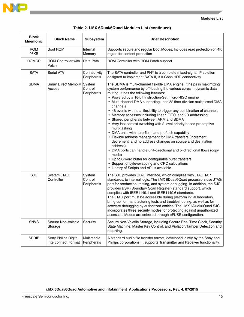
ROM96KB
Boot ROM Internal Memory
Supports secure and regular Boot Modes. Includes read protection on 4K region for content protection
ROMCP ROM Controller with Patch
Data Path ROM Controller with ROM Patch support
SATA Serial ATA Connectivity Peripherals
The SATA controller and PHY is a complete mixed-signal IP solution designed to implement SATA II, 3.0 Gbps HDD connectivity.
SDMA Smart Direct Memory Access
System Control Peripherals
The SDMA is multi-channel flexible DMA engine. It helps in maximizing system performance by off-loading the various cores in dynamic data routing. It has the following features: • Powered by a 16-bit Instruction-Set micro-RISC engine • Multi-channel DMA supporting up to 32 time-division multiplexed DMA
channels • 48 events with total flexibility to trigger any combination of channels • Memory accesses including linear, FIFO, and 2D addressing • Shared peripherals between ARM and SDMA • Very fast context-switching with 2-level priority based preemptive
multi-tasking • DMA units with auto-flush and prefetch capability • Flexible address management for DMA transfers (increment,
decrement, and no address changes on source and destination address)
• DMA ports can handle unit-directional and bi-directional flows (copy mode)
• Up to 8-word buffer for configurable burst transfers • Support of byte-swapping and CRC calculations • Library of Scripts and API is available
SJC System JTAG Controller
System Control Peripherals
The SJC provides JTAG interface, which complies with JTAG TAP standards, to internal logic. The i.MX 6Dual/6Quad processors use JTAG port for production, testing, and system debugging. In addition, the SJC provides BSR (Boundary Scan Register) standard support, which complies with IEEE1149.1 and IEEE1149.6 standards. The JTAG port must be accessible during platform initial laboratory bring-up, for manufacturing tests and troubleshooting, as well as for software debugging by authorized entities. The i.MX 6Dual/6Quad SJC incorporates three security modes for protecting against unauthorized accesses. Modes are selected through eFUSE configuration.
SNVS Secure Non-Volatile Storage
Security Secure Non-Volatile Storage, including Secure Real Time Clock, Security State Machine, Master Key Control, and Violation/Tamper Detection and reporting.
SPDIF Sony Philips Digital Interconnect Format
Multimedia Peripherals
A standard audio file transfer format, developed jointly by the Sony and Phillips corporations. It supports Transmitter and Receiver functionality.
Table 2. i.MX 6Dual/6Quad Modules List (continued)
Block Mnemonic
Block Name Subsystem Brief Description
i.MX 6Dual/6Quad Automotive and Infotainment Applications Processors, Rev. 4, 07/2015
16 Freescale Semiconductor Inc.
Modules List
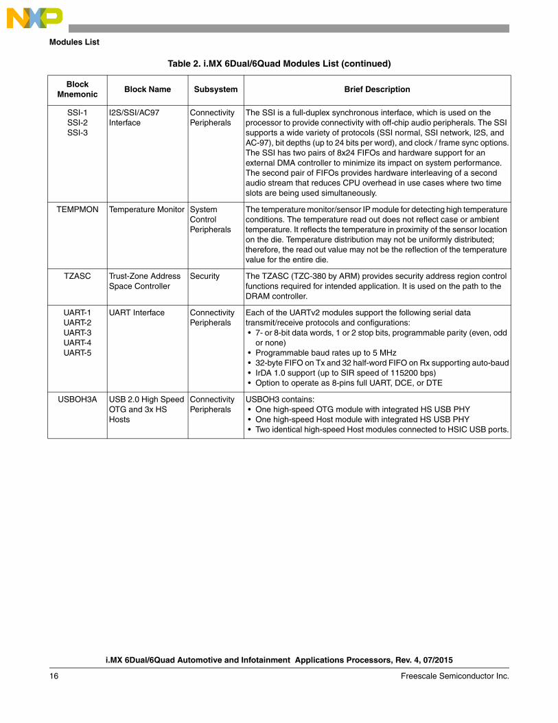
SSI-1SSI-2SSI-3
I2S/SSI/AC97 Interface
Connectivity Peripherals
The SSI is a full-duplex synchronous interface, which is used on the processor to provide connectivity with off-chip audio peripherals. The SSI supports a wide variety of protocols (SSI normal, SSI network, I2S, and AC-97), bit depths (up to 24 bits per word), and clock / frame sync options.The SSI has two pairs of 8x24 FIFOs and hardware support for an external DMA controller to minimize its impact on system performance. The second pair of FIFOs provides hardware interleaving of a second audio stream that reduces CPU overhead in use cases where two time slots are being used simultaneously.
TEMPMON Temperature Monitor System Control Peripherals
The temperature monitor/sensor IP module for detecting high temperature conditions. The temperature read out does not reflect case or ambient temperature. It reflects the temperature in proximity of the sensor location on the die. Temperature distribution may not be uniformly distributed; therefore, the read out value may not be the reflection of the temperature value for the entire die.
TZASC Trust-Zone Address Space Controller
Security The TZASC (TZC-380 by ARM) provides security address region control functions required for intended application. It is used on the path to the DRAM controller.
UART-1UART-2UART-3UART-4UART-5
UART Interface Connectivity Peripherals
Each of the UARTv2 modules support the following serial data transmit/receive protocols and configurations: • 7- or 8-bit data words, 1 or 2 stop bits, programmable parity (even, odd
or none) • Programmable baud rates up to 5 MHz • 32-byte FIFO on Tx and 32 half-word FIFO on Rx supporting auto-baud • IrDA 1.0 support (up to SIR speed of 115200 bps) • Option to operate as 8-pins full UART, DCE, or DTE
USBOH3A USB 2.0 High Speed OTG and 3x HS Hosts
Connectivity Peripherals
USBOH3 contains: • One high-speed OTG module with integrated HS USB PHY • One high-speed Host module with integrated HS USB PHY • Two identical high-speed Host modules connected to HSIC USB ports.
Table 2. i.MX 6Dual/6Quad Modules List (continued)
Block Mnemonic
Block Name Subsystem Brief Description
Modules List
i.MX 6Dual/6Quad Automotive and Infotainment Applications Processors, Rev. 4, 07/2015
Freescale Semiconductor Inc. 17
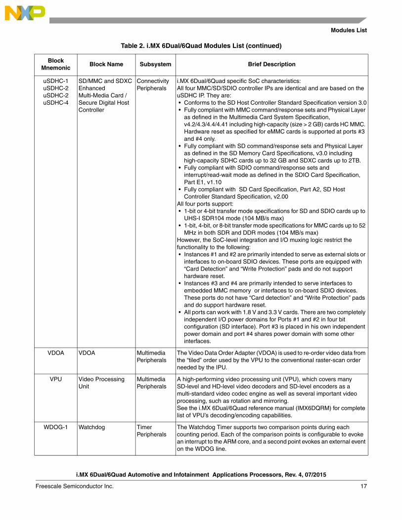
uSDHC-1uSDHC-2uSDHC-2uSDHC-4
SD/MMC and SDXCEnhanced Multi-Media Card / Secure Digital Host Controller
Connectivity Peripherals
i.MX 6Dual/6Quad specific SoC characteristics:All four MMC/SD/SDIO controller IPs are identical and are based on the uSDHC IP. They are: • Conforms to the SD Host Controller Standard Specification version 3.0 • Fully compliant with MMC command/response sets and Physical Layer
as defined in the Multimedia Card System Specification, v4.2/4.3/4.4/4.41 including high-capacity (size > 2 GB) cards HC MMC. Hardware reset as specified for eMMC cards is supported at ports #3 and #4 only.
• Fully compliant with SD command/response sets and Physical Layer as defined in the SD Memory Card Specifications, v3.0 including high-capacity SDHC cards up to 32 GB and SDXC cards up to 2TB.
• Fully compliant with SDIO command/response sets and interrupt/read-wait mode as defined in the SDIO Card Specification, Part E1, v1.10
• Fully compliant with SD Card Specification, Part A2, SD Host Controller Standard Specification, v2.00
All four ports support: • 1-bit or 4-bit transfer mode specifications for SD and SDIO cards up to
UHS-I SDR104 mode (104 MB/s max) • 1-bit, 4-bit, or 8-bit transfer mode specifications for MMC cards up to 52
MHz in both SDR and DDR modes (104 MB/s max)However, the SoC-level integration and I/O muxing logic restrict the functionality to the following: • Instances #1 and #2 are primarily intended to serve as external slots or
interfaces to on-board SDIO devices. These ports are equipped with “Card Detection” and “Write Protection” pads and do not support hardware reset.
• Instances #3 and #4 are primarily intended to serve interfaces to embedded MMC memory or interfaces to on-board SDIO devices. These ports do not have “Card detection” and “Write Protection” pads and do support hardware reset.
• All ports can work with 1.8 V and 3.3 V cards. There are two completely independent I/O power domains for Ports #1 and #2 in four bit configuration (SD interface). Port #3 is placed in his own independent power domain and port #4 shares power domain with some other interfaces.
VDOA VDOA Multimedia Peripherals
The Video Data Order Adapter (VDOA) is used to re-order video data from the “tiled” order used by the VPU to the conventional raster-scan order needed by the IPU.
VPU Video Processing Unit
Multimedia Peripherals
A high-performing video processing unit (VPU), which covers many SD-level and HD-level video decoders and SD-level encoders as a multi-standard video codec engine as well as several important video processing, such as rotation and mirroring.See the i.MX 6Dual/6Quad reference manual (IMX6DQRM) for complete list of VPU’s decoding/encoding capabilities.
WDOG-1 Watchdog Timer Peripherals
The Watchdog Timer supports two comparison points during each counting period. Each of the comparison points is configurable to evoke an interrupt to the ARM core, and a second point evokes an external event on the WDOG line.
Table 2. i.MX 6Dual/6Quad Modules List (continued)
Block Mnemonic
Block Name Subsystem Brief Description
i.MX 6Dual/6Quad Automotive and Infotainment Applications Processors, Rev. 4, 07/2015
18 Freescale Semiconductor Inc.
Modules List
3.1 Special Signal ConsiderationsThe package contact assignments can be found in Section 6, “Package Information and Contact Assignments.” Signal descriptions are defined in the i.MX 6Dual/6Quad reference manual (IMX6DQRM). Special signal consideration information is contained in the Hardware Development Guide for i.MX 6Quad, 6Dual, 6DualLite, 6Solo Families of Applications Processors (IMX6DQ6SDLHDG).
3.2 Recommended Connections for Unused Analog InterfacesThe recommended connections for unused analog interfaces can be found in the section, “Unused analog interfaces,” of the Hardware Development Guide for i.MX 6Quad, 6Dual, 6DualLite, 6Solo Families of Applications Processors (IMX6DQ6SDLHDG).
WDOG-2(TZ)
Watchdog (TrustZone)
Timer Peripherals
The TrustZone Watchdog (TZ WDOG) timer module protects against TrustZone starvation by providing a method of escaping normal mode and forcing a switch to the TZ mode. TZ starvation is a situation where the normal OS prevents switching to the TZ mode. Such a situation is undesirable as it can compromise the system’s security. Once the TZ WDOG module is activated, it must be serviced by TZ software on a periodic basis. If servicing does not take place, the timer times out. Upon a time-out, the TZ WDOG asserts a TZ mapped interrupt that forces switching to the TZ mode. If it is still not served, the TZ WDOG asserts a security violation signal to the CSU. The TZ WDOG module cannot be programmed or deactivated by a normal mode Software.
EIM NOR-Flash /PSRAM interface
Connectivity Peripherals
The EIM NOR-FLASH / PSRAM provides: • Support 16-bit (in muxed IO mode only) PSRAM memories (sync and
async operating modes), at slow frequency • Support 16-bit (in muxed IO mode only) NOR-Flash memories, at slow
frequency • Multiple chip selects
XTALOSC Crystal Oscillator interface
— The XTALOSC module enables connectivity to external crystal oscillator device. In a typical application use-case, it is used for 24 MHz oscillator.
Table 2. i.MX 6Dual/6Quad Modules List (continued)
Block Mnemonic
Block Name Subsystem Brief Description
Electrical Characteristics
i.MX 6Dual/6Quad Automotive and Infotainment Applications Processors, Rev. 4, 07/2015
Freescale Semiconductor Inc. 19
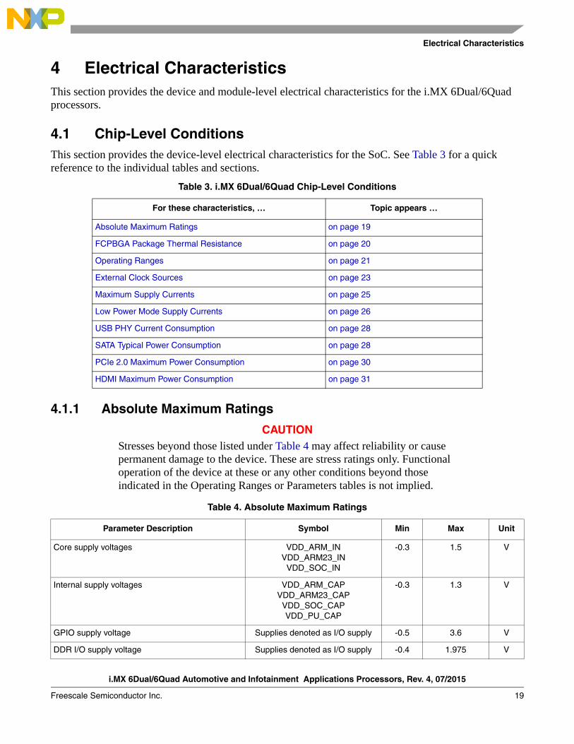
4 Electrical CharacteristicsThis section provides the device and module-level electrical characteristics for the i.MX 6Dual/6Quad processors.
4.1 Chip-Level ConditionsThis section provides the device-level electrical characteristics for the SoC. See Table 3 for a quick reference to the individual tables and sections.
4.1.1 Absolute Maximum Ratings
CAUTIONStresses beyond those listed under Table 4 may affect reliability or cause permanent damage to the device. These are stress ratings only. Functional operation of the device at these or any other conditions beyond those indicated in the Operating Ranges or Parameters tables is not implied.
Table 3. i.MX 6Dual/6Quad Chip-Level Conditions
For these characteristics, … Topic appears …
Absolute Maximum Ratings on page 19
FCPBGA Package Thermal Resistance on page 20
Operating Ranges on page 21
External Clock Sources on page 23
Maximum Supply Currents on page 25
Low Power Mode Supply Currents on page 26
USB PHY Current Consumption on page 28
SATA Typical Power Consumption on page 28
PCIe 2.0 Maximum Power Consumption on page 30
HDMI Maximum Power Consumption on page 31
Table 4. Absolute Maximum Ratings
Parameter Description Symbol Min Max Unit
Core supply voltages VDD_ARM_INVDD_ARM23_IN
VDD_SOC_IN
-0.3 1.5 V
Internal supply voltages VDD_ARM_CAPVDD_ARM23_CAP
VDD_SOC_CAPVDD_PU_CAP
-0.3 1.3 V
GPIO supply voltage Supplies denoted as I/O supply -0.5 3.6 V
DDR I/O supply voltage Supplies denoted as I/O supply -0.4 1.975 V
i.MX 6Dual/6Quad Automotive and Infotainment Applications Processors, Rev. 4, 07/2015
20 Freescale Semiconductor Inc.
Electrical Characteristics
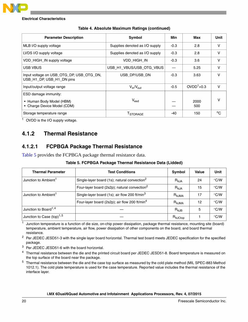
4.1.2 Thermal Resistance
4.1.2.1 FCPBGA Package Thermal Resistance
Table 5 provides the FCPBGA package thermal resistance data.
MLB I/O supply voltage Supplies denoted as I/O supply -0.3 2.8 V
LVDS I/O supply voltage Supplies denoted as I/O supply -0.3 2.8 V
VDD_HIGH_IN supply voltage VDD_HIGH_IN -0.3 3.6 V
USB VBUS USB_H1_VBUS/USB_OTG_VBUS — 5.25 V
Input voltage on USB_OTG_DP, USB_OTG_DN, USB_H1_DP, USB_H1_DN pins
USB_DP/USB_DN -0.3 3.63 V
Input/output voltage range Vin/Vout -0.5 OVDD1+0.3 V
ESD damage immunity:
Vesd V • Human Body Model (HBM) • Charge Device Model (CDM)
——
2000500
Storage temperature range TSTORAGE -40 150 oC
1 OVDD is the I/O supply voltage.
Table 5. FCPBGA Package Thermal Resistance Data (Lidded)
Thermal Parameter Test Conditions Symbol Value Unit
Junction to Ambient1
1 Junction temperature is a function of die size, on-chip power dissipation, package thermal resistance, mounting site (board) temperature, ambient temperature, air flow, power dissipation of other components on the board, and board thermal resistance.
Single-layer board (1s); natural convection2
2 Per JEDEC JESD51-3 with the single layer board horizontal. Thermal test board meets JEDEC specification for the specified package.
RθJA 24 °C/W
Four-layer board (2s2p); natural convection2 RθJA 15 °C/W
Junction to Ambient1 Single-layer board (1s); air flow 200 ft/min3
3 Per JEDEC JESD51-6 with the board horizontal.
RθJMA 17 °C/W
Four-layer board (2s2p); air flow 200 ft/min4 RθJMA 12 °C/W
Junction to Board1,4
4 Thermal resistance between the die and the printed circuit board per JEDEC JESD51-8. Board temperature is measured on the top surface of the board near the package.
— RθJB 5 °C/W
Junction to Case (top)1,5
5 Thermal resistance between the die and the case top surface as measured by the cold plate method (MIL SPEC-883 Method 1012.1). The cold plate temperature is used for the case temperature. Reported value includes the thermal resistance of the interface layer.
— RθJCtop 1 °C/W
Table 4. Absolute Maximum Ratings (continued)
Parameter Description Symbol Min Max Unit
Electrical Characteristics
i.MX 6Dual/6Quad Automotive and Infotainment Applications Processors, Rev. 4, 07/2015
Freescale Semiconductor Inc. 21
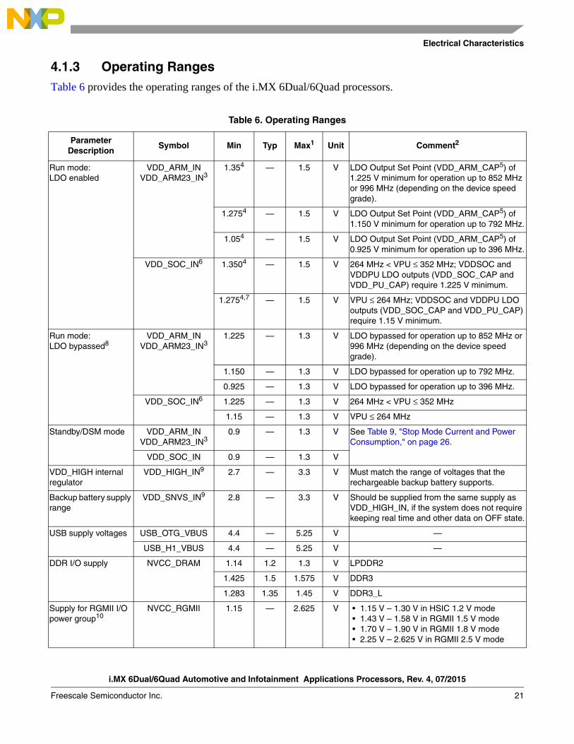
4.1.3 Operating RangesTable 6 provides the operating ranges of the i.MX 6Dual/6Quad processors.
Table 6. Operating Ranges
Parameter Description
Symbol Min Typ Max1 Unit Comment2
Run mode: LDO enabled
VDD_ARM_INVDD_ARM23_IN3
1.354 — 1.5 V LDO Output Set Point (VDD_ARM_CAP5) of 1.225 V minimum for operation up to 852 MHz or 996 MHz (depending on the device speed grade).
1.2754 — 1.5 V LDO Output Set Point (VDD_ARM_CAP5) of 1.150 V minimum for operation up to 792 MHz.
1.054 — 1.5 V LDO Output Set Point (VDD_ARM_CAP5) of 0.925 V minimum for operation up to 396 MHz.
VDD_SOC_IN6 1.3504 — 1.5 V 264 MHz < VPU ≤ 352 MHz; VDDSOC and VDDPU LDO outputs (VDD_SOC_CAP and VDD_PU_CAP) require 1.225 V minimum.
1.2754,7 — 1.5 V VPU ≤ 264 MHz; VDDSOC and VDDPU LDO outputs (VDD_SOC_CAP and VDD_PU_CAP) require 1.15 V minimum.
Run mode: LDO bypassed8
VDD_ARM_INVDD_ARM23_IN3
1.225 — 1.3 V LDO bypassed for operation up to 852 MHz or 996 MHz (depending on the device speed grade).
1.150 — 1.3 V LDO bypassed for operation up to 792 MHz.
0.925 — 1.3 V LDO bypassed for operation up to 396 MHz.
VDD_SOC_IN6 1.225 — 1.3 V 264 MHz < VPU ≤ 352 MHz
1.15 — 1.3 V VPU ≤ 264 MHz
Standby/DSM mode VDD_ARM_IN VDD_ARM23_IN3
0.9 — 1.3 V See Table 9, "Stop Mode Current and Power Consumption," on page 26.
VDD_SOC_IN 0.9 — 1.3 V
VDD_HIGH internal regulator
VDD_HIGH_IN9 2.7 — 3.3 V Must match the range of voltages that the rechargeable backup battery supports.
Backup battery supply range
VDD_SNVS_IN9 2.8 — 3.3 V Should be supplied from the same supply as VDD_HIGH_IN, if the system does not require keeping real time and other data on OFF state.
USB supply voltages USB_OTG_VBUS 4.4 — 5.25 V —
USB_H1_VBUS 4.4 — 5.25 V —
DDR I/O supply NVCC_DRAM 1.14 1.2 1.3 V LPDDR2
1.425 1.5 1.575 V DDR3
1.283 1.35 1.45 V DDR3_L
Supply for RGMII I/O power group10
NVCC_RGMII 1.15 — 2.625 V • 1.15 V – 1.30 V in HSIC 1.2 V mode • 1.43 V – 1.58 V in RGMII 1.5 V mode • 1.70 V – 1.90 V in RGMII 1.8 V mode • 2.25 V – 2.625 V in RGMII 2.5 V mode
i.MX 6Dual/6Quad Automotive and Infotainment Applications Processors, Rev. 4, 07/2015
22 Freescale Semiconductor Inc.
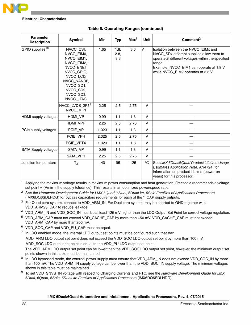
Electrical Characteristics
GPIO supplies10 NVCC_CSI,NVCC_EIM0,NVCC_EIM1,NVCC_EIM2,NVCC_ENET,NVCC_GPIO,NVCC_LCD,
NVCC_NANDF,NVCC_SD1,NVCC_SD2,NVCC_SD3,NVCC_JTAG
1.65 1.8,2.8,3.3
3.6 V Isolation between the NVCC_EIMx and NVCC_SDx different supplies allow them to operate at different voltages within the specified range.Example: NVCC_EIM1 can operate at 1.8 V while NVCC_EIM2 operates at 3.3 V.
NVCC_LVDS_2P511
NVCC_MIPI2.25 2.5 2.75 V —
HDMI supply voltages HDMI_VP 0.99 1.1 1.3 V —
HDMI_VPH 2.25 2.5 2.75 V —
PCIe supply voltages PCIE_VP 1.023 1.1 1.3 V —
PCIE_VPH 2.325 2.5 2.75 V —
PCIE_VPTX 1.023 1.1 1.3 V —
SATA Supply voltages SATA_VP 0.99 1.1 1.3 V —
SATA_VPH 2.25 2.5 2.75 V —
Junction temperature TJ -40 95 125 °C See i.MX 6Dual/6Quad Product Lifetime Usage Estimates Application Note, AN4724, for information on product lifetime (power-on years) for this processor.
1 Applying the maximum voltage results in maximum power consumption and heat generation. Freescale recommends a voltage set point = (Vmin + the supply tolerance). This results in an optimized power/speed ratio.
2 See the Hardware Development Guide for i.MX 6Quad, 6Dual, 6DualLite, 6Solo Families of Applications Processors (IMX6DQ6SDLHDG) for bypass capacitors requirements for each of the *_CAP supply outputs.
3 For Quad core system, connect to VDD_ARM_IN. For Dual core system, may be shorted to GND together with VDD_ARM23_CAP to reduce leakage.
4 VDD_ARM_IN and VDD_SOC_IN must be at least 125 mV higher than the LDO Output Set Point for correct voltage regulation.5 VDD_ARM_CAP must not exceed VDD_CACHE_CAP by more than +50 mV. VDD_CACHE_CAP must not exceed
VDD_ARM_CAP by more than 200 mV.6 VDD_SOC_CAP and VDD_PU_CAP must be equal.7 In LDO enabled mode, the internal LDO output set points must be configured such that the:
VDD_ARM LDO output set point does not exceed the VDD_SOC LDO output set point by more than 100 mV.
VDD_SOC LDO output set point is equal to the VDD_PU LDO output set point.The VDD_ARM LDO output set point can be lower than the VDD_SOC LDO output set point, however, the minimum output set points shown in this table must be maintained.
8 In LDO bypassed mode, the external power supply must ensure that VDD_ARM_IN does not exceed VDD_SOC_IN by more than 100 mV. The VDD_ARM_IN supply voltage can be lower than the VDD_SOC_IN supply voltage. The minimum voltages shown in this table must be maintained.
9 To set VDD_SNVS_IN voltage with respect to Charging Currents and RTC, see the Hardware Development Guide for i.MX 6Dual, 6Quad, 6Solo, 6DualLite Families of Applications Processors (IMX6DQ6SDLHDG).
Table 6. Operating Ranges (continued)
Parameter Description
Symbol Min Typ Max1 Unit Comment2
Electrical Characteristics
i.MX 6Dual/6Quad Automotive and Infotainment Applications Processors, Rev. 4, 07/2015
Freescale Semiconductor Inc. 23
4.1.4 External Clock Sources
Each i.MX 6Dual/6Quad processor has two external input system clocks: a low frequency (RTC_XTALI) and a high frequency (XTALI).
The RTC_XTALI is used for low-frequency functions. It supplies the clock for wake-up circuit, power-down real time clock operation, and slow system and watchdog counters. The clock input can be connected to either an external oscillator or a crystal using the internal oscillator amplifier. Additionally, there is an internal ring oscillator, that can be used instead of RTC_XTALI when accuracy is not important.
The system clock input XTALI is used to generate the main system clock. It supplies the PLLs and other peripherals. The system clock input can be connected to either an external oscillator or a crystal using the internal oscillator amplifier.
NOTEThe internal RTC oscillator does not provide an accurate frequency and is affected by process, voltage and temperature variations. Freescale strongly recommends using an external crystal as the RTC_XTALI reference. If the internal oscillator is used instead, careful consideration should be given to the timing implications on all of the SoC modules dependent on this clock.
Table 7 shows the interface frequency requirements.
The typical values shown in Table 7 are required for use with Freescale BSPs to ensure precise time keeping and USB operation. For RTC_XTALI operation, two clock sources are available:
• On-chip 40 kHz ring oscillator: This clock source has the following characteristics:
— Approximately 25 μA more Idd than crystal oscillator
— Approximately ±50% tolerance
— No external component required
— Starts up quicker than 32 kHz crystal oscillator
• External crystal oscillator with on-chip support circuit
10 All digital I/O supplies (NVCC_xxxx) must be powered under normal conditions whether the associated I/O pins are in use or not, and associated I/O pins need to have a pull-up or pull-down resistor applied to limit any floating gate current.
11 This supply also powers the pre-drivers of the DDR I/O pins; therefore, it must always be provided, even when LVDS is not used.
Table 7. External Input Clock Frequency
Parameter Description Symbol Min Typ Max Unit
RTC_XTALI Oscillator1,2
1 External oscillator or a crystal with internal oscillator amplifier.2 The required frequency stability of this clock source is application dependent. For recommendations, see the Hardware
Development Guide for i.MX 6Dual, 6Quad, 6Solo, 6DualLite Families of Applications Processors (IMX6DQ6SDLHDG).
fckil — 32.7683/32.0
3 Recommended nominal frequency 32.768 kHz.
— kHz
XTALI Oscillator4,2
4 External oscillator or a fundamental frequency crystal with internal oscillator amplifier.
fxtal — 24 — MHz
i.MX 6Dual/6Quad Automotive and Infotainment Applications Processors, Rev. 4, 07/2015
24 Freescale Semiconductor Inc.
Electrical Characteristics
— At power up, an internal ring oscillator is used. After crystal oscillator is stable, the clock circuit switches over to the crystal oscillator automatically.
— Higher accuracy than ring oscillator.
— If no external crystal is present, then the ring oscillator is used.
The decision to choose a clock source should be based on real-time clock use and precision timeout.
4.1.5 Maximum Supply Currents
Power consumption is highly dependent on the application. Estimating the maximum supply currents required for power supply design is difficult because the use case that requires maximum supply current is not a realistic use case.
To help illustrate the effect of the application on power consumption, data was collected while running industry standard benchmarks that are designed to be compute and graphic intensive. The results provided are intended to be used as guidelines for power supply design.
Description of test conditions:
• The Power Virus data shown in Table 8 represent a use case designed specifically to show the maximum current consumption possible for the ARM core complex. All cores are running at the defined maximum frequency and are limited to L1 cache accesses only to ensure no pipeline stalls. Although a valid condition, it would have a very limited, if any, practical use case, and be limited to an extremely low duty cycle unless the intention was to specifically cause the worst case power consumption.
• EEMBC CoreMark: Benchmark designed specifically for the purpose of measuring the performance of a CPU core. More information available at www.eembc.org/coremark. Note that this benchmark is designed as a core performance benchmark, not a power benchmark. This use case is provided as an example of power consumption that would be typical in a computationally-intensive application rather than the Power Virus.
• 3DMark Mobile 2011: Suite of benchmarks designed for the purpose of measuring graphics and overall system performance. More information available at www.rightware.com/benchmarks. Note that this benchmark is designed as a graphics performance benchmark, not a power benchmark. This use case is provided as an example of power consumption that would be typical in a very graphics-intensive application.
• Devices used for the tests were from the high current end of the expected process variation.
The Freescale power management IC, MMPF0100xxxx, which is targeted for the i.MX 6 series processor family, supports the power consumption shown in Table 8, however a robust thermal design is required for the increased system power dissipation.
See the i.MX 6Dual/6Quad Power Consumption Measurement Application Note (AN4509) for more details on typical power consumption under various use case definitions.
Electrical Characteristics
i.MX 6Dual/6Quad Automotive and Infotainment Applications Processors, Rev. 4, 07/2015
Freescale Semiconductor Inc. 25
Table 8. Maximum Supply Currents
Power Supply Conditions Maximum Current
UnitPower Virus CoreMark
i.MX 6Quad: VDD_ARM_IN + VDD_ARM23_IN
• ARM frequency = 996 MHz • ARM LDOs set to 1.3V • Tj = 125°C
3920 2500 mA
• ARM frequency = 852 MHz • ARM LDOs set to 1.3V • Tj = 125°C
3630 2260 mA
i.MX 6Dual: VDD_ARM_IN • ARM frequency = 996 MHz • ARM LDOs set to 1.3V • Tj = 125°C
2350 1500 mA
• ARM frequency = 852 MHz • ARM LDOs set to 1.3V • Tj = 125°C
2110 1360 mA
i.MX 6Dual: or i.MX 6Quad: VDD_SOC_IN
• Running 3DMark • GPU frequency = 600 MHz • SOC LDO set to 1.3V • Tj = 125°C
2500 mA
VDD_HIGH_IN — 1251 mA
VDD_SNVS_IN — 2752 μA
USB_OTG_VBUS/USB_H1_VBUS (LDO 3P0)
— 253 mA
Primary Interface (IO) Supplies
NVCC_DRAM — (see note4)
NVCC_ENET N=10 Use maximum IO equation5
NVCC_LCD N=29 Use maximum IO equation5
NVCC_GPIO N=24 Use maximum IO equation5
NVCC_CSI N=20 Use maximum IO equation5
NVCC_EIM0 N=19 Use maximum IO equation5
NVCC_EIM1 N=14 Use maximum IO equation5
NVCC_EIM2 N=20 Use maximum IO equation5
NVCC_JTAG N=6 Use maximum IO equation5
NVCC_RGMII N=6 Use maximum IO equation5
NVCC_SD1 N=6 Use maximum IO equation5
NVCC_SD2 N=6 Use maximum IO equation5
NVCC_SD3 N=11 Use maximum IO equation5
NVCC_NANDF N=26 Use maximum IO equation5
NVCC_MIPI — 25.5 mA
i.MX 6Dual/6Quad Automotive and Infotainment Applications Processors, Rev. 4, 07/2015
26 Freescale Semiconductor Inc.
Electrical Characteristics
4.1.6 Low Power Mode Supply CurrentsTable 9 shows the current core consumption (not including I/O) of the i.MX 6Dual/6Quad processors in selected low power modes.
NVCC_LVDS2P5 — NVCC_LVDS2P5 is connected to VDD_HIGH_CAP at the board level. VDD_HIGH_CAP is capable of handing the current required by NVCC_LVDS2P5.
MISC
DRAM_VREF — 1 mA
1 The actual maximum current drawn from VDD_HIGH_IN will be as shown plus any additional current drawn from the VDD_HIGH_CAP outputs, depending upon actual application configuration (for example, NVCC_LVDS_2P5, NVCC_MIPI, or HDMI, PCIe, and SATA VPH supplies).
2 Under normal operating conditions, the maximum current on VDD_SNVS_IN is shown Table 8. The maximum VDD_SNVS_IN current may be higher depending on specific operating configurations, such as BOOT_MODE[1:0] not equal to 00, or use of the Tamper feature. During initial power on, VDD_SNVS_IN can draw up to 1 mA if the supply is capable of sourcing that current. If less than 1 mA is available, the VDD_SNVS_CAP charge time will increase.
3 This is the maximum current per active USB physical interface.4 The DRAM power consumption is dependent on several factors such as external signal termination. DRAM power calculators
are typically available from memory vendors which take into account factors such as signal termination.See the i.MX 6Dual/6Quad Power Consumption Measurement Application Note (AN4509) for examples of DRAM power consumption during specific use case scenarios.
5 General equation for estimated, maximum power consumption of an IO power supply:Imax = N x C x V x (0.5 x F)Where:N—Number of IO pins supplied by the power lineC—Equivalent external capacitive loadV—IO voltage(0.5 xF)—Data change rate. Up to 0.5 of the clock rate (F)In this equation, Imax is in Amps, C in Farads, V in Volts, and F in Hertz.
Table 9. Stop Mode Current and Power Consumption
Mode Test Conditions Supply Typical1 Unit
WAIT • ARM, SoC, and PU LDOs are set to 1.225 V • HIGH LDO set to 2.5 V • Clocks are gated • DDR is in self refresh • PLLs are active in bypass (24 MHz) • Supply voltages remain ON
VDD_ARM_IN (1.4 V) 6 mA
VDD_SOC_IN (1.4 V) 23 mA
VDD_HIGH_IN (3.0 V) 3.7 mA
Total 52 mW
Table 8. Maximum Supply Currents (continued)
Power Supply Conditions Maximum Current
UnitPower Virus CoreMark
Electrical Characteristics
i.MX 6Dual/6Quad Automotive and Infotainment Applications Processors, Rev. 4, 07/2015
Freescale Semiconductor Inc. 27
STOP_ON • ARM LDO set to 0.9 V • SoC and PU LDOs set to 1.225 V • HIGH LDO set to 2.5 V • PLLs disabled • DDR is in self refresh
VDD_ARM_IN (1.4 V) 7.5 mA
VDD_SOC_IN (1.4 V) 22 mA
VDD_HIGH_IN (3.0 V) 3.7 mA
Total 52 mW
STOP_OFF • ARM LDO set to 0.9 V • SoC LDO set to 1.225 V • PU LDO is power gated • HIGH LDO set to 2.5 V • PLLs disabled • DDR is in self refresh
VDD_ARM_IN (1.4 V) 7.5 mA
VDD_SOC_IN (1.4 V) 13.5 mA
VDD_HIGH_IN (3.0 V) 3.7 mA
Total 41 mW
STANDBY • ARM and PU LDOs are power gated • SoC LDO is in bypass • HIGH LDO is set to 2.5 V • PLLs are disabled • Low voltage • Well Bias ON • Crystal oscillator is enabled
VDD_ARM_IN (0.9 V) 0.1 mA
VDD_SOC_IN (0.9 V) 13 mA
VDD_HIGH_IN (3.0 V) 3.7 mA
Total 22 mW
Deep Sleep Mode(DSM)
• ARM and PU LDOs are power gated • SoC LDO is in bypass • HIGH LDO is set to 2.5 V • PLLs are disabled • Low voltage • Well Bias ON • Crystal oscillator and bandgap are disabled
VDD_ARM_IN (0.9 V) 0.1 mA
VDD_SOC_IN (0.9 V) 2 mA
VDD_HIGH_IN (3.0 V) 0.5 mA
Total 3.4 mW
SNVS Only • VDD_SNVS_IN powered • All other supplies off • SRTC running
VDD_SNVS_IN (2.8V) 41 μA
Total 115 μW
1 The typical values shown here are for information only and are not guaranteed. These values are average values measured on a worst-case wafer at 25°C.
Table 9. Stop Mode Current and Power Consumption (continued)
Mode Test Conditions Supply Typical1 Unit
i.MX 6Dual/6Quad Automotive and Infotainment Applications Processors, Rev. 4, 07/2015
28 Freescale Semiconductor Inc.
Electrical Characteristics
4.1.7 USB PHY Current Consumption
4.1.7.1 Power Down Mode
In power down mode, everything is powered down, including the VBUS valid detectors, typ condition. Table 10 shows the USB interface current consumption in power down mode.
NOTEThe currents on the VDD_HIGH_CAP and VDD_USB_CAP were identified to be the voltage divider circuits in the USB-specific level shifters.
4.1.8 SATA Typical Power Consumption
Table 11 provides SATA PHY currents for certain Tx operating modes.
NOTETx power consumption values are provided for a single transceiver. If T = single transceiver power and C = Clock module power, the total power required for N lanes = N x T + C.
Table 10. USB PHY Current Consumption in Power Down Mode
VDD_USB_CAP (3.0 V) VDD_HIGH_CAP (2.5 V) NVCC_PLL_OUT (1.1 V)
Current 5.1 μA 1.7 μA <0.5 μA
Table 11. SATA PHY Current Drain
Mode Test Conditions Supply Typical Current Unit
P0: Full-power state1 Single Transceiver SATA_VP 11 mA
SATA_VPH 13
Clock Module SATA_VP 6.9
SATA_VPH 6.2
P0: Mobile2 Single Transceiver SATA_VP 11 mA
SATA_VPH 11
Clock Module SATA_VP 6.9
SATA_VPH 6.2
P0s: Transmitter idle Single Transceiver SATA_VP 9.4 mA
SATA_VPH 2.9
Clock Module SATA_VP 6.9
SATA_VPH 6.2
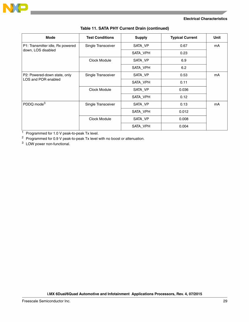
Electrical Characteristics
i.MX 6Dual/6Quad Automotive and Infotainment Applications Processors, Rev. 4, 07/2015
Freescale Semiconductor Inc. 29
P1: Transmitter idle, Rx powered down, LOS disabled
Single Transceiver SATA_VP 0.67 mA
SATA_VPH 0.23
Clock Module SATA_VP 6.9
SATA_VPH 6.2
P2: Powered-down state, only LOS and POR enabled
Single Transceiver SATA_VP 0.53 mA
SATA_VPH 0.11
Clock Module SATA_VP 0.036
SATA_VPH 0.12
PDDQ mode3 Single Transceiver SATA_VP 0.13 mA
SATA_VPH 0.012
Clock Module SATA_VP 0.008
SATA_VPH 0.004
1 Programmed for 1.0 V peak-to-peak Tx level.2 Programmed for 0.9 V peak-to-peak Tx level with no boost or attenuation.3 LOW power non-functional.
Table 11. SATA PHY Current Drain (continued)
Mode Test Conditions Supply Typical Current Unit
i.MX 6Dual/6Quad Automotive and Infotainment Applications Processors, Rev. 4, 07/2015
30 Freescale Semiconductor Inc.
Electrical Characteristics
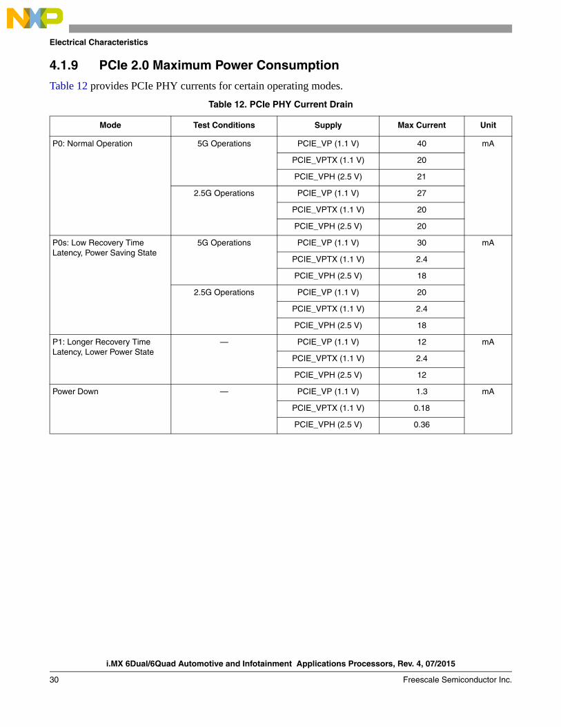
4.1.9 PCIe 2.0 Maximum Power Consumption
Table 12 provides PCIe PHY currents for certain operating modes.
Table 12. PCIe PHY Current Drain
Mode Test Conditions Supply Max Current Unit
P0: Normal Operation 5G Operations PCIE_VP (1.1 V) 40 mA
PCIE_VPTX (1.1 V) 20
PCIE_VPH (2.5 V) 21
2.5G Operations PCIE_VP (1.1 V) 27
PCIE_VPTX (1.1 V) 20
PCIE_VPH (2.5 V) 20
P0s: Low Recovery Time Latency, Power Saving State
5G Operations PCIE_VP (1.1 V) 30 mA
PCIE_VPTX (1.1 V) 2.4
PCIE_VPH (2.5 V) 18
2.5G Operations PCIE_VP (1.1 V) 20
PCIE_VPTX (1.1 V) 2.4
PCIE_VPH (2.5 V) 18
P1: Longer Recovery Time Latency, Lower Power State
— PCIE_VP (1.1 V) 12 mA
PCIE_VPTX (1.1 V) 2.4
PCIE_VPH (2.5 V) 12
Power Down — PCIE_VP (1.1 V) 1.3 mA
PCIE_VPTX (1.1 V) 0.18
PCIE_VPH (2.5 V) 0.36
Electrical Characteristics
i.MX 6Dual/6Quad Automotive and Infotainment Applications Processors, Rev. 4, 07/2015
Freescale Semiconductor Inc. 31
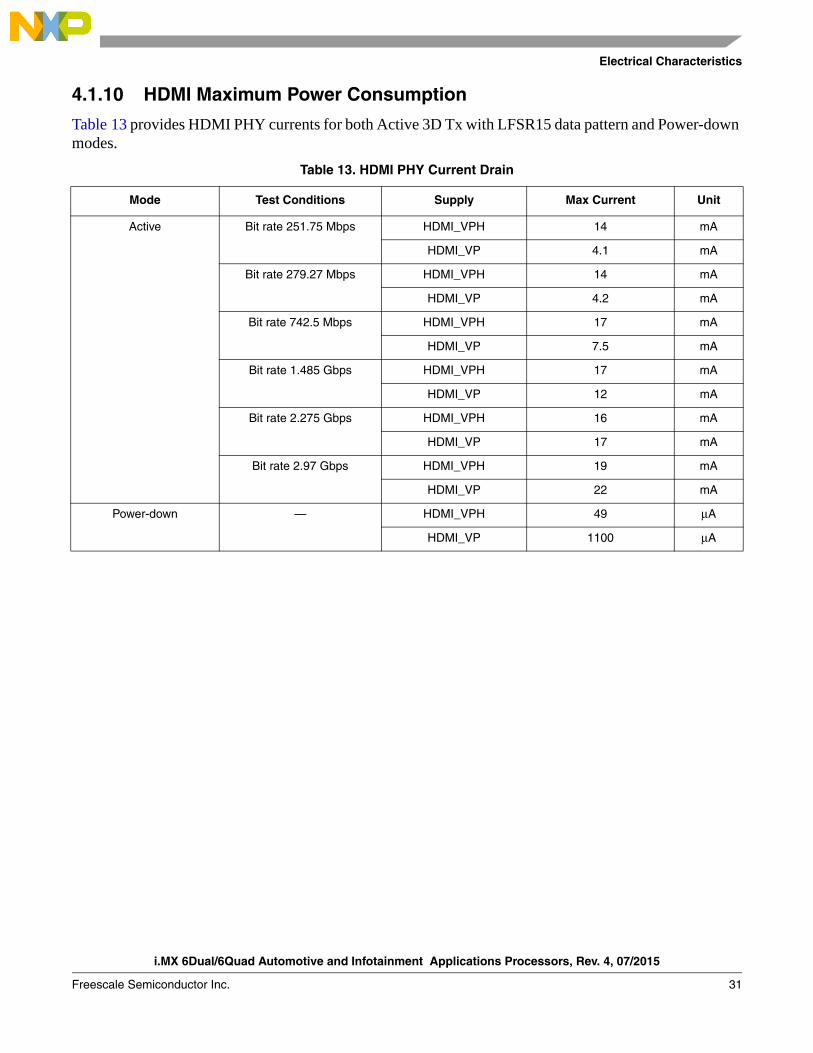
4.1.10 HDMI Maximum Power Consumption
Table 13 provides HDMI PHY currents for both Active 3D Tx with LFSR15 data pattern and Power-down modes.
Table 13. HDMI PHY Current Drain
Mode Test Conditions Supply Max Current Unit
Active Bit rate 251.75 Mbps HDMI_VPH 14 mA
HDMI_VP 4.1 mA
Bit rate 279.27 Mbps HDMI_VPH 14 mA
HDMI_VP 4.2 mA
Bit rate 742.5 Mbps HDMI_VPH 17 mA
HDMI_VP 7.5 mA
Bit rate 1.485 Gbps HDMI_VPH 17 mA
HDMI_VP 12 mA
Bit rate 2.275 Gbps HDMI_VPH 16 mA
HDMI_VP 17 mA
Bit rate 2.97 Gbps HDMI_VPH 19 mA
HDMI_VP 22 mA
Power-down — HDMI_VPH 49 μA
HDMI_VP 1100 μA
i.MX 6Dual/6Quad Automotive and Infotainment Applications Processors, Rev. 4, 07/2015
32 Freescale Semiconductor Inc.
Electrical Characteristics
4.2 Power Supplies Requirements and RestrictionsThe system design must comply with power-up sequence, power-down sequence, and steady state guidelines as described in this section to ensure the reliable operation of the device. Any deviation from these sequences may result in the following situations:
• Excessive current during power-up phase
• Prevention of the device from booting
• Irreversible damage to the processor
4.2.1 Power-Up SequenceFor power-up sequence, the restrictions are as follows:
• VDD_SNVS_IN supply must be turned ON before any other power supply. It may be connected (shorted) with VDD_HIGH_IN supply.
• If a coin cell is used to power VDD_SNVS_IN, then ensure that it is connected before any other supply is switched on.
• If the external SRC_POR_B signal is used to control the processor POR, then SRC_POR_B must be immediately asserted at power-up and remain asserted until the VDD_ARM_CAP, VDD_SOC_CAP, and VDD_PU_CAP supplies are stable. VDD_ARM_IN and VDD_SOC_IN may be applied in either order with no restrictions. In the absence of an external reset feeding the SRC_POR_B input, the internal POR module takes control. See the i.MX 6Dual/6Quad reference manual (IMX6DQRM) for further details and to ensure that all necessary requirements are being met.
• If the external SRC_POR_B signal is not used (always held high or left unconnected), the processor defaults to the internal POR function (where the PMU controls generation of the POR based on the power supplies). If the internal POR function is used, the following power supply requirements must be met:
— VDD_ARM_IN and VDD_SOC_IN may be supplied from the same source, or
— VDD_SOC_IN can be supplied before VDD_ARM_IN with a maximum delay of 1 ms.
NOTEEnsure that there is no back voltage (leakage) from any supply on the board towards the 3.3 V supply (for example, from the external components that use both the 1.8 V and 3.3 V supplies).
NOTEUSB_OTG_VBUS and USB_H1_VBUS are not part of the power supply sequence and can be powered at any time.
4.2.2 Power-Down Sequence
No special restrictions for i.MX 6Dual/6Quad SoC.
Electrical Characteristics
i.MX 6Dual/6Quad Automotive and Infotainment Applications Processors, Rev. 4, 07/2015
Freescale Semiconductor Inc. 33
4.2.3 Power Supplies Usage• All I/O pins should not be externally driven while the I/O power supply for the pin (NVCC_xxx)
is OFF. This can cause internal latch-up and malfunctions due to reverse current flows. For information about I/O power supply of each pin, see “Power Group” column of Table 100, "21 x 21 mm Functional Contact Assignments," on page 149.
• When the SATA interface is not used, the SATA_VP and SATA_VPH supplies should be grounded. The input and output supplies for rest of the ports (SATA_REXT, SATA_PHY_RX_N, SATA_PHY_RX_P, and SATA_PHY_TX_N) can be left floating. It is recommended not to turn OFF the SATA_VPH supply while the SATA_VP supply is ON, as it may lead to excessive power consumption. If boundary scan test is used, SATA_VP and SATA_VPH must remain powered.
• When the PCIE interface is not used, the PCIE_VP, PCIE_VPH, and PCIE_VPTX supplies should be grounded. The input and output supplies for rest of the ports (PCIE_REXT, PCIE_RX_N, PCIE_RX_P, PCIE_TX_N, and PCIE_TX_P) can be left floating. It is recommended not to turn the PCIE_VPH supply OFF while the PCIE_VP supply is ON, as it may lead to excessive power consumption. If boundary scan test is used, PCIE_VP, PCIE_VPH, and PCIE_VPTX must remain powered.
4.3 Integrated LDO Voltage Regulator ParametersVarious internal supplies can be powered ON from internal LDO voltage regulators. All the supply pins named *_CAP must be connected to external capacitors. The onboard LDOs are intended for internal use only and should not be used to power any external circuitry. See the i.MX 6Dual/6Quad reference manual (IMX6DQRM) for details on the power tree scheme recommended operation.
NOTEThe *_CAP signals should not be powered externally. These signals are intended for internal LDO or LDO bypass operation only.
4.3.1 Digital Regulators (LDO_ARM, LDO_PU, LDO_SOC)
There are three digital LDO regulators (“Digital”, because of the logic loads that they drive, not because of their construction). The advantages of the regulators are to reduce the input supply variation because of their input supply ripple rejection and their on die trimming. This translates into more voltage for the die producing higher operating frequencies. These regulators have three basic modes.
• Bypass. The regulation FET is switched fully on passing the external voltage, DCDC_LOW, to the load unaltered. The analog part of the regulator is powered down in this state, removing any loss other than the IR drop through the power grid and FET.
• Power Gate. The regulation FET is switched fully off limiting the current draw from the supply. The analog part of the regulator is powered down here limiting the power consumption.
• Analog regulation mode. The regulation FET is controlled such that the output voltage of the regulator equals the programmed target voltage. The target voltage is fully programmable in 25 mV steps.
i.MX 6Dual/6Quad Automotive and Infotainment Applications Processors, Rev. 4, 07/2015
34 Freescale Semiconductor Inc.
Electrical Characteristics
Optionally LDO_SOC and VDD_SOC_CAP can be used to power the HDMI, PCIe, and SATA PHY's through external connections.
For additional information, see the i.MX 6Dual/6Quad reference manual (IMX6DQRM).
4.3.2 Regulators for Analog Modules
4.3.2.1 LDO_1P1
The LDO_1P1 regulator implements a programmable linear-regulator function from VDD_HIGH_IN (see Table 6 for minimum and maximum input requirements). Typical Programming Operating Range is 1.0 V to 1.2 V with the nominal default setting as 1.1 V. The LDO_1P1 supplies the USB PHY, LVDS PHY, HDMI PHY, MIPI PHY, and PLLs. A programmable brown-out detector is included in the regulator that can be used by the system to determine when the load capability of the regulator is being exceeded to take the necessary steps. Current-limiting can be enabled to allow for in-rush current requirements during start-up, if needed. Active-pull-down can also be enabled for systems requiring this feature.
For information on external capacitor requirements for this regulator, see the Hardware Development Guide for i.MX 6Quad, 6Dual, 6DualLite, 6Solo Families of Applications Processors (IMX6DQ6SDLHDG).
For additional information, see the i.MX 6Dual/6Quad reference manual (IMX6DQRM).
4.3.2.2 LDO_2P5
The LDO_2P5 module implements a programmable linear-regulator function from VDD_HIGH_IN (see Table 6 for min and max input requirements). Typical Programming Operating Range is 2.25 V to 2.75 V with the nominal default setting as 2.5 V. The LDO_2P5 supplies the SATA PHY, USB PHY, LVDS PHY, HDMI PHY, MIPI PHY, E-fuse module and PLLs. A programmable brown-out detector is included in the regulator that can be used by the system to determine when the load capability of the regulator is being exceeded, to take the necessary steps. Current-limiting can be enabled to allow for in-rush current requirements during start-up, if needed. Active-pull-down can also be enabled for systems requiring this feature. An alternate self-biased low-precision weak-regulator is included that can be enabled for applications needing to keep the output voltage alive during low-power modes where the main regulator driver and its associated global bandgap reference module are disabled. The output of the weak-regulator is not programmable and is a function of the input supply as well as the load current. Typically, with a 3 V input supply the weak-regulator output is 2.525 V and its output impedance is approximately 40 Ω.
For information on external capacitor requirements for this regulator, see the Hardware Development Guide for i.MX 6Quad, 6Dual, 6DualLite, 6Solo Families of Applications Processors (IMX6DQ6SDLHDG).
For additional information, see the i.MX 6Dual/6Quad reference manual (IMX6DQRM).
4.3.2.3 LDO_USB
The LDO_USB module implements a programmable linear-regulator function from the USB_OTG_VBUS and USB_H1_VBUS voltages (4.4 V–5.25 V) to produce a nominal 3.0 V output
Electrical Characteristics
i.MX 6Dual/6Quad Automotive and Infotainment Applications Processors, Rev. 4, 07/2015
Freescale Semiconductor Inc. 35
voltage. A programmable brown-out detector is included in the regulator that can be used by the system to determine when the load capability of the regulator is being exceeded, to take the necessary steps. This regulator has a built in power-mux that allows the user to select to run the regulator from either VBUS supply, when both are present. If only one of the VBUS voltages is present, then the regulator automatically selects this supply. Current limit is also included to help the system meet in-rush current targets. If no VBUS voltage is present, then the VBUSVALID threshold setting will prevent the regulator from being enabled.
For information on external capacitor requirements for this regulator, see the Hardware Development Guide for i.MX 6Quad, 6Dual, 6DualLite, 6Solo Families of Applications Processors (IMX6DQ6SDLHDG).
For additional information, see the i.MX 6Dual/6Quad reference manual (IMX6DQRM).
4.4 PLL Electrical Characteristics
4.4.1 Audio/Video PLL Electrical Parameters
4.4.2 528 MHz PLL
4.4.3 Ethernet PLL
Table 14. Audio/Video PLL Electrical Parameters
Parameter Value
Clock output range 650 MHz ~1.3 GHz
Reference clock 24 MHz
Lock time <11250 reference cycles
Table 15. 528 MHz PLL Electrical Parameters
Parameter Value
Clock output range 528 MHz PLL output
Reference clock 24 MHz
Lock time <11250 reference cycles
Table 16. Ethernet PLL Electrical Parameters
Parameter Value
Clock output range 500 MHz
Reference clock 24 MHz
Lock time <11250 reference cycles
i.MX 6Dual/6Quad Automotive and Infotainment Applications Processors, Rev. 4, 07/2015
36 Freescale Semiconductor Inc.
Electrical Characteristics
4.4.4 480 MHz PLL
4.4.5 MLB PLL
The MediaLB PLL is necessary in the MediaLB 6-Pin implementation to phase align the internal and external clock edges, effectively tuning out the delay of the differential clock receiver and is also responsible for generating the higher speed internal clock, when the internal-to-external clock ratio is not 1:1.
4.4.6 ARM PLL
4.5 On-Chip Oscillators
4.5.1 OSC24M
This block implements an amplifier that when combined with a suitable quartz crystal and external load capacitors implements an oscillator. The oscillator is powered from NVCC_PLL_OUT.
The system crystal oscillator consists of a Pierce-type structure running off the digital supply. A straight forward biased-inverter implementation is used.
4.5.2 OSC32K
This block implements an amplifier that when combined with a suitable quartz crystal and external load capacitors implements a low power oscillator. It also implements a power mux such that it can be powered
Table 17. 480 MHz PLL Electrical Parameters
Parameter Value
Clock output range 480 MHz PLL output
Reference clock 24 MHz
Lock time <383 reference cycles
Table 18. MLB PLL Electrical Parameters
Parameter Value
Lock time <1.5 ms
Table 19. ARM PLL Electrical Parameters
Parameter Value
Clock output range 650 MHz~1.3 GHz
Reference clock 24 MHz
Lock time <2250 reference cycles
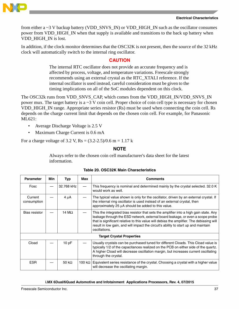
Electrical Characteristics
i.MX 6Dual/6Quad Automotive and Infotainment Applications Processors, Rev. 4, 07/2015
Freescale Semiconductor Inc. 37
from either a ~3 V backup battery (VDD_SNVS_IN) or VDD_HIGH_IN such as the oscillator consumes power from VDD_HIGH_IN when that supply is available and transitions to the back up battery when VDD_HIGH_IN is lost.
In addition, if the clock monitor determines that the OSC32K is not present, then the source of the 32 kHz clock will automatically switch to the internal ring oscillator.
CAUTIONThe internal RTC oscillator does not provide an accurate frequency and is affected by process, voltage, and temperature variations. Freescale strongly recommends using an external crystal as the RTC_XTALI reference. If the internal oscillator is used instead, careful consideration must be given to the timing implications on all of the SoC modules dependent on this clock.
The OSC32k runs from VDD_SNVS_CAP, which comes from the VDD_HIGH_IN/VDD_SNVS_IN power mux. The target battery is a ~3 V coin cell. Proper choice of coin cell type is necessary for chosen VDD_HIGH_IN range. Appropriate series resistor (Rs) must be used when connecting the coin cell. Rs depends on the charge current limit that depends on the chosen coin cell. For example, for Panasonic ML621:
• Average Discharge Voltage is 2.5 V
• Maximum Charge Current is 0.6 mA
For a charge voltage of 3.2 V, Rs = (3.2-2.5)/0.6 m = 1.17 k
NOTEAlways refer to the chosen coin cell manufacturer's data sheet for the latest information.
Table 20. OSC32K Main Characteristics
Parameter Min Typ Max Comments
Fosc — 32.768 kHz — This frequency is nominal and determined mainly by the crystal selected. 32.0 K would work as well.
Current consumption
— 4 μA — The typical value shown is only for the oscillator, driven by an external crystal. If the internal ring oscillator is used instead of an external crystal, then approximately 25 μA should be added to this value.
Bias resistor — 14 MΩ — This the integrated bias resistor that sets the amplifier into a high gain state. Any leakage through the ESD network, external board leakage, or even a scope probe that is significant relative to this value will debias the amplifier. The debiasing will result in low gain, and will impact the circuit's ability to start up and maintain oscillations.
Target Crystal Properties
Cload — 10 pF — Usually crystals can be purchased tuned for different Cloads. This Cload value is typically 1/2 of the capacitances realized on the PCB on either side of the quartz. A higher Cload will decrease oscillation margin, but increases current oscillating through the crystal.
ESR — 50 kΩ 100 kΩ Equivalent series resistance of the crystal. Choosing a crystal with a higher value will decrease the oscillating margin.
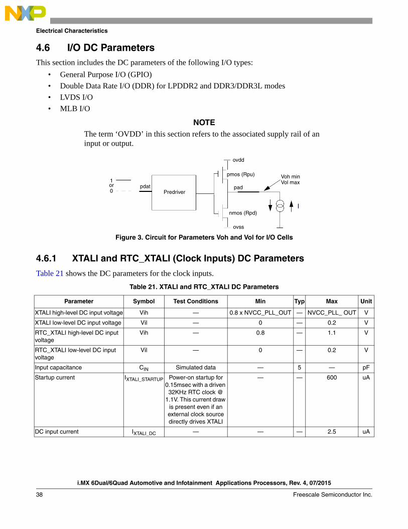
i.MX 6Dual/6Quad Automotive and Infotainment Applications Processors, Rev. 4, 07/2015
38 Freescale Semiconductor Inc.
Electrical Characteristics
4.6 I/O DC ParametersThis section includes the DC parameters of the following I/O types:
• General Purpose I/O (GPIO)
• Double Data Rate I/O (DDR) for LPDDR2 and DDR3/DDR3L modes
• LVDS I/O
• MLB I/O
NOTEThe term ‘OVDD’ in this section refers to the associated supply rail of an input or output.
Figure 3. Circuit for Parameters Voh and Vol for I/O Cells
4.6.1 XTALI and RTC_XTALI (Clock Inputs) DC Parameters
Table 21 shows the DC parameters for the clock inputs.
Table 21. XTALI and RTC_XTALI DC Parameters
Parameter Symbol Test Conditions Min Typ Max Unit
XTALI high-level DC input voltage Vih — 0.8 x NVCC_PLL_OUT — NVCC_PLL_ OUT V
XTALI low-level DC input voltage Vil — 0 — 0.2 V
RTC_XTALI high-level DC input voltage
Vih — 0.8 — 1.1 V
RTC_XTALI low-level DC input voltage
Vil — 0 — 0.2 V
Input capacitance CIN Simulated data — 5 — pF
Startup current IXTALI_STARTUP Power-on startup for 0.15msec with a driven 32KHz RTC clock @
1.1V. This current draw is present even if an external clock source directly drives XTALI
— — 600 uA
DC input current IXTALI_DC — — — 2.5 uA
0or1
Predriverpdat
ovdd
pad
nmos (Rpd)
ovss
Voh minVol max
pmos (Rpu)
Electrical Characteristics
i.MX 6Dual/6Quad Automotive and Infotainment Applications Processors, Rev. 4, 07/2015
Freescale Semiconductor Inc. 39
4.6.2 General Purpose I/O (GPIO) DC Parameters
Table 22 shows DC parameters for GPIO pads. The parameters in Table 22 are guaranteed per the operating ranges in Table 6, unless otherwise noted.
4.6.3 DDR I/O DC Parameters
The DDR I/O pads support LPDDR2 and DDR3/DDR3L operational modes.
Table 22. GPIO I/O DC Parameters
Parameter Symbol Test Conditions Min Max Unit
High-level output voltage1
1 Overshoot and undershoot conditions (transitions above OVDD and below GND) on switching pads must be held below 0.6 V, and the duration of the overshoot/undershoot must not exceed 10% of the system clock cycle. Overshoot/ undershoot must be controlled through printed circuit board layout, transmission line impedance matching, signal line termination, or other methods. Non-compliance to this specification may affect device reliability or cause permanent damage to the device.
Voh Ioh = -0.1 mA (DSE2 = 001, 010)Ioh = -1 mA
(DSE = 011, 100, 101, 110, 111)
2 DSE is the Drive Strength Field setting in the associated IOMUX control register.
OVDD – 0.15 — V
Low-level output voltage1 Vol Iol = 0.1 mA (DSE2 = 001, 010)Iol = 1mA
(DSE = 011, 100, 101, 110, 111)
— 0.15 V
High-Level DC input voltage1, 3
3 To maintain a valid level, the transition edge of the input must sustain a constant slew rate (monotonic) from the current DC level through to the target DC level, Vil or Vih. Monotonic input transition time is from 0.1 ns to 1 s.
Vih — 0.7 × OVDD OVDD V
Low-Level DC input voltage1, 3 Vil — 0 0.3 × OVDD V
Input Hysteresis Vhys OVDD = 1.8 VOVDD = 3.3 V
0.25 — V
Schmitt trigger VT+3, 4
4 Hysteresis of 250 mV is guaranteed over all operating conditions when hysteresis is enabled.
VT+ — 0.5 × OVDD — V
Schmitt trigger VT–3, 4 VT– — — 0.5 × OVDD V
Input current (no pull-up/down) Iin Vin = OVDD or 0 -1 1 μA
Input current (22 kΩ pull-up) Iin Vin = 0 VVin = OVDD
— 2121
μA
Input current (47 kΩ pull-up) Iin Vin = 0 VVin = OVDD
— 1001
μA
Input current (100 kΩ pull-up) Iin Vin = 0 VVin= OVDD
— 481
μA
Input current (100 kΩ pull-down) Iin Vin = 0 VVin = OVDD
— 148
μA
Keeper circuit resistance Rkeep Vin = 0.3 x OVDDVin = 0.7 x OVDD
105 175kΩ
i.MX 6Dual/6Quad Automotive and Infotainment Applications Processors, Rev. 4, 07/2015
40 Freescale Semiconductor Inc.
Electrical Characteristics
4.6.3.1 LPDDR2 Mode I/O DC Parameters
The LPDDR2 interface mode fully complies with JESD209-2B LPDDR2 JEDEC standard release June, 2009. The parameters in Table 23 are guaranteed per the operating ranges in Table 6, unless otherwise noted.
4.6.3.2 DDR3/DDR3L Mode I/O DC Parameters
The DDR3/DDR3L interface mode fully complies with JESD79-3D DDR3 JEDEC standard release April, 2008. The parameters in Table 24 are guaranteed per the operating ranges in Table 6, unless otherwise noted.
Table 23. LPDDR2 I/O DC Electrical Parameters1
1 Note that the JEDEC LPDDR2 specification (JESD209_2B) supersedes any specification in this document.
Parameters Symbol Test Conditions Min Max Unit
High-level output voltage Voh Ioh = -0.1 mA 0.9 × OVDD — V
Low-level output voltage Vol Iol = 0.1 mA — 0.1 × OVDD V
Input reference voltage Vref — 0.49 × OVDD 0.51 × OVDD
DC input High Voltage Vih(dc) — Vref+0.13V OVDD V
DC input Low Voltage Vil(dc) — OVSS Vref-0.13V V
Differential Input Logic High Vih(diff) — 0.26 See Note 2
2 The single-ended signals need to be within the respective limits (Vih(dc) max, Vil(dc) min) for single-ended signals as well as the limitations for overshoot and undershoot (see Table 29).
—
Differential Input Logic Low Vil(diff) — See Note 2 -0.26 —
Input current (no pull-up/down) Iin Vin = 0 or OVDD -2.5 2.5 μA
Pull-up/pull-down impedance mismatch MMpupd — -15 +15 %
240 Ω unit calibration resolution Rres — — 10 Ω
Keeper circuit resistance Rkeep — 110 175 kΩ
Table 24. DDR3/DDR3L I/O DC Electrical Parameters
Parameters Symbol Test Conditions Min Max Unit
High-level output voltage
Voh
Ioh = -0.1 mAVoh (DSE = 001)
0.8 × OVDD1 — VIoh = -1 mA
Voh (for all except DSE = 001)
Low-level output voltage
Vol
Iol = 0.1 mAVol (DSE = 001)
— 0.2 × OVDD VIol = 1 mA
Vol (for all except DSE = 001)
Input reference voltage Vref2 — 0.49 × OVDD 0.51 × OVDD
DC input Logic High Vih(dc) — Vref+0.1 OVDD V
Electrical Characteristics
i.MX 6Dual/6Quad Automotive and Infotainment Applications Processors, Rev. 4, 07/2015
Freescale Semiconductor Inc. 41
4.6.4 LVDS I/O DC Parameters
The LVDS interface complies with TIA/EIA 644-A standard. See TIA/EIA STANDARD 644-A, “Electrical Characteristics of Low Voltage Differential Signaling (LVDS) Interface Circuits” for details.
Table 25 shows the Low Voltage Differential Signalling (LVDS) I/O DC parameters.
4.6.5 MLB 6-Pin I/O DC Parameters
The MLB interface complies with Analog Interface of 6-pin differential Media Local Bus specification version 4.1. See 6-pin differential MLB specification v4.1, “MediaLB 6-pin interface Electrical Characteristics” for details.
NOTEThe MLB 6-pin interface does not support speed mode 8192fs.
Table 26 shows the Media Local Bus (MLB) I/O DC parameters.
DC input Logic Low Vil(dc) — OVSS Vref-0.1 V
Differential input Logic High Vih(diff) — 0.2 See Note3 V
Differential input Logic Low Vil(diff) — See Note3 -0.2 V
Termination Voltage Vtt Vtt tracking OVDD/2 0.49 × OVDD 0.51 × OVDD V
Input current (no pull-up/down) Iin Vin = 0 or OVDD -2.9 2.9 μA
Pull-up/pull-down impedance mismatch MMpupd — -10 10 %
240 Ω unit calibration resolution Rres — — 10 Ω
Keeper circuit resistance Rkeep — 105 175 kΩ1 OVDD – I/O power supply (1.425 V–1.575 V for DDR3 and 1.283 V–1.45 V for DDR3L).2 Vref – DDR3/DDR3L external reference voltage.3 The single-ended signals need to be within the respective limits (Vih(dc) max, Vil(dc) min) for single-ended signals as well as
the limitations for overshoot and undershoot (see Table 30).
Table 25. LVDS I/O DC Parameters
Parameter Symbol Test Conditions Min Max Unit
Output Differential Voltage VOD Rload=100 Ω between padP and padN 250 450 mV
Output High Voltage VOH IOH = 0 mA 1.25 1.6
VOutput Low Voltage VOL IOL = 0 mA 0.9 1.25
Offset Voltage VOS — 1.125 1.375
Table 24. DDR3/DDR3L I/O DC Electrical Parameters (continued)
Parameters Symbol Test Conditions Min Max Unit
i.MX 6Dual/6Quad Automotive and Infotainment Applications Processors, Rev. 4, 07/2015
42 Freescale Semiconductor Inc.
Electrical Characteristics
4.7 I/O AC ParametersThis section includes the AC parameters of the following I/O types:
• General Purpose I/O (GPIO)
• Double Data Rate I/O (DDR) for LPDDR2 and DDR3/DDR3L modes
• LVDS I/O
• MLB I/O
The GPIO and DDR I/O load circuit and output transition time waveforms are shown in Figure 4 and Figure 5.
Figure 4. Load Circuit for Output
Figure 5. Output Transition Time Waveform
Table 26. MLB I/O DC Parameters
Parameter Symbol Test Conditions Min Max Unit
Output Differential Voltage VOD Rload = 50 Ω between padP and padN 300 500 mV
Output High Voltage VOH 1.15 1.75 V
Output Low Voltage VOL 0.75 1.35 V
Common-mode Output Voltage ((Vpad_P + Vpad_N) / 2))
VOCM 1 1.5V
Differential Output Impedance ZO — 1.6 — kΩ
Test PointFrom Output
CL
CL includes package, probe and fixture capacitance
Under Test
0 V
OVDD
20%
80% 80%
20%
tr tfOutput (at pad)
Electrical Characteristics
i.MX 6Dual/6Quad Automotive and Infotainment Applications Processors, Rev. 4, 07/2015
Freescale Semiconductor Inc. 43
4.7.1 General Purpose I/O AC Parameters
The I/O AC parameters for GPIO in slow and fast modes are presented in the Table 27 and Table 28, respectively. Note that the fast or slow I/O behavior is determined by the appropriate control bits in the IOMUXC control registers.
Table 27. General Purpose I/O AC Parameters 1.8 V Mode
Parameter Symbol Test Condition Min Typ Max Unit
Output Pad Transition Times, rise/fall(Max Drive, ipp_dse=111)
tr, tf 15 pF Cload, slow slew rate15 pF Cload, fast slew rate
— —2.72/2.791.51/1.54
ns
Output Pad Transition Times, rise/fall(High Drive, ipp_dse=101)
tr, tf 15 pF Cload, slow slew rate15 pF Cload, fast slew rate
— —3.20/3.361.96/2.07
Output Pad Transition Times, rise/fall(Medium Drive, ipp_dse=100)
tr, tf 15 pF Cload, slow slew rate15 pF Cload, fast slew rate
— —3.64/3.882.27/2.53
Output Pad Transition Times, rise/fall(Low Drive. ipp_dse=011)
tr, tf 15 pF Cload, slow slew rate15 pF Cload, fast slew rate
— —4.32/4.503.16/3.17
Input Transition Times1
1 Hysteresis mode is recommended for inputs with transition times greater than 25 ns.
trm — — — 25 ns
Table 28. General Purpose I/O AC Parameters 3.3 V Mode
Parameter Symbol Test Condition Min Typ Max Unit
Output Pad Transition Times, rise/fall(Max Drive, ipp_dse=101)
tr, tf 15 pF Cload, slow slew rate15 pF Cload, fast slew rate
— —1.70/1.791.06/1.15
ns
Output Pad Transition Times, rise/fall(High Drive, ipp_dse=011)
tr, tf 15 pF Cload, slow slew rate15 pF Cload, fast slew rate
— —2.35/2.431.74/1.77
Output Pad Transition Times, rise/fall(Medium Drive, ipp_dse=010)
tr, tf 15 pF Cload, slow slew rate15 pF Cload, fast slew rate
— —3.13/3.292.46/2.60
Output Pad Transition Times, rise/fall(Low Drive. ipp_dse=001)
tr, tf 15 pF Cload, slow slew rate15 pF Cload, fast slew rate
— —5.14/5.574.77/5.15
Input Transition Times1
1 Hysteresis mode is recommended for inputs with transition times greater than 25 ns.
trm — — — 25 ns
i.MX 6Dual/6Quad Automotive and Infotainment Applications Processors, Rev. 4, 07/2015
44 Freescale Semiconductor Inc.
Electrical Characteristics
4.7.2 DDR I/O AC Parameters
The LPDDR2 interface mode fully complies with JESD209-2B LPDDR2 JEDEC standard release June, 2009. The DDR3/DDR3L interface mode fully complies with JESD79-3D DDR3 JEDEC standard release April, 2008.
Table 29 shows the AC parameters for DDR I/O operating in LPDDR2 mode.
Table 30 shows the AC parameters for DDR I/O operating in DDR3/DDR3L mode.
Table 29. DDR I/O LPDDR2 Mode AC Parameters1
1 Note that the JEDEC LPDDR2 specification (JESD209_2B) supersedes any specification in this document.
Parameter Symbol Test Condition Min Typ Max Unit
AC input logic high Vih(ac) — Vref + 0.22 — OVDD V
AC input logic low Vil(ac) — 0 — Vref – 0.22 V
AC differential input high voltage2
2 Vid(ac) specifies the input differential voltage |Vtr – Vcp| required for switching, where Vtr is the “true” input signal and Vcp is the “complementary” input signal. The Minimum value is equal to Vih(ac) – Vil(ac).
Vidh(ac) — 0.44 — — V
AC differential input low voltage Vidl(ac) — — — 0.44 V
Input AC differential cross point voltage3
3 The typical value of Vix(ac) is expected to be about 0.5 × OVDD. and Vix(ac) is expected to track variation of OVDD. Vix(ac) indicates the voltage at which differential input signal must cross.
Vix(ac) Relative to Vref -0.12 — 0.12 V
Over/undershoot peak Vpeak — — — 0.35 V
Over/undershoot area (above OVDDor below OVSS)
Varea 533 MHz — — 0.3 V-ns
Single output slew rate, measured between Vol(ac) and Voh(ac)
tsr 50 Ω to Vref.5 pF load.
Drive impedance = 4 0 Ω ±30%
1.5 — 3.5 V/ns
50 Ω to Vref.5pF load.
Drive impedance = 60 Ω ±30%
1 — 2.5
Skew between pad rise/fall asymmetry + skew caused by SSN
tSKD clk = 533 MHz — — 0.1 ns
Table 30. DDR I/O DDR3/DDR3L Mode AC Parameters1
Parameter Symbol Test Condition Min Typ Max Unit
AC input logic high Vih(ac) — Vref + 0.175 — OVDD V
AC input logic low Vil(ac) — 0 — Vref – 0.175 V
AC differential input voltage2 Vid(ac) — 0.35 — — V
Input AC differential cross point voltage3 Vix(ac) Relative to Vref Vref – 0.15 — Vref + 0.15 V
Over/undershoot peak Vpeak — — — 0.4 V
Over/undershoot area (above OVDDor below OVSS)
Varea 533 MHz — — 0.5 V-ns
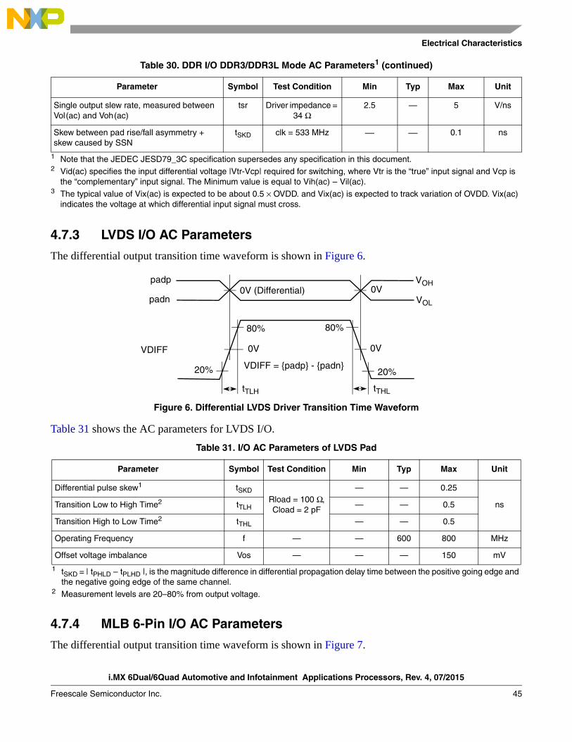
Electrical Characteristics
i.MX 6Dual/6Quad Automotive and Infotainment Applications Processors, Rev. 4, 07/2015
Freescale Semiconductor Inc. 45
4.7.3 LVDS I/O AC Parameters
The differential output transition time waveform is shown in Figure 6.
Figure 6. Differential LVDS Driver Transition Time Waveform
Table 31 shows the AC parameters for LVDS I/O.
4.7.4 MLB 6-Pin I/O AC Parameters
The differential output transition time waveform is shown in Figure 7.
Single output slew rate, measured between Vol(ac) and Voh(ac)
tsr Driver impedance = 34 Ω
2.5 — 5 V/ns
Skew between pad rise/fall asymmetry + skew caused by SSN
tSKD clk = 533 MHz — — 0.1 ns
1 Note that the JEDEC JESD79_3C specification supersedes any specification in this document.2 Vid(ac) specifies the input differential voltage |Vtr-Vcp| required for switching, where Vtr is the “true” input signal and Vcp is
the “complementary” input signal. The Minimum value is equal to Vih(ac) – Vil(ac).3 The typical value of Vix(ac) is expected to be about 0.5 × OVDD. and Vix(ac) is expected to track variation of OVDD. Vix(ac)
indicates the voltage at which differential input signal must cross.
Table 31. I/O AC Parameters of LVDS Pad
Parameter Symbol Test Condition Min Typ Max Unit
Differential pulse skew1
1 tSKD = | tPHLD – tPLHD |, is the magnitude difference in differential propagation delay time between the positive going edge and the negative going edge of the same channel.
tSKDRload = 100 Ω,Cload = 2 pF
— — 0.25
nsTransition Low to High Time2
2 Measurement levels are 20–80% from output voltage.
tTLH — — 0.5
Transition High to Low Time2 tTHL — — 0.5
Operating Frequency f — — 600 800 MHz
Offset voltage imbalance Vos — — — 150 mV
Table 30. DDR I/O DDR3/DDR3L Mode AC Parameters1 (continued)
Parameter Symbol Test Condition Min Typ Max Unit
padp
padn
VDIFF
0V (Differential)
VDIFF = {padp} - {padn}
tTLH
20%
80%
20%
80%
tTHL
VOH
VOL
0V
0V
0V
i.MX 6Dual/6Quad Automotive and Infotainment Applications Processors, Rev. 4, 07/2015
46 Freescale Semiconductor Inc.
Electrical Characteristics
Figure 7. Differential MLB Driver Transition Time Waveform
A 4-stage pipeline is used in the MLB 6-pin implementation to facilitate design, maximize throughput, and allow for reasonable PCB trace lengths. Each cycle is one ipp_clk_in* (internal clock from MLB PLL) clock period. Cycles 2, 3, and 4 are MLB PHY related. Cycle 2 includes clock-to-output delay of Signal/Data sampling flip-flop and Transmitter, Cycle 3 includes clock-to-output delay of Signal/Data clocked receiver, Cycle 4 includes clock-to-output delay of Signal/Data sampling flip-flop.
MLB 6-pin pipeline diagram is shown in Figure 8.
Figure 8. MLB 6-Pin Pipeline Diagram
Table 32 shows the AC parameters for MLB I/O.
Table 32. I/O AC Parameters of MLB PHY
Parameter Symbol Test Condition Min Typ Max Unit
Differential pulse skew1
1 tSKD = | tPHLD – tPLHD |, is the magnitude difference in differential propagation delay time between the positive going edge and the negative going edge of the same channel.
tSKD Rload = 50 Ω between padP
and padN
— — 0.1
nsTransition Low to High Time2
2 Measurement levels are 20-80% from output voltage.
tTLH — — 1
Transition High to Low Time tTHL — — 1
MLB external clock Operating Frequency fclk_ext — — — 102.4 MHz
MLB PLL clock Operating Frequency fclk_pll — — — 307.2 MHz
padp
padn
VDIFF
0V (Differential)
VDIFF = {padp} - {padn}
tTLH
20%
80%
20%
80%
tTHL
VOH
VOL
0V
0V
0V
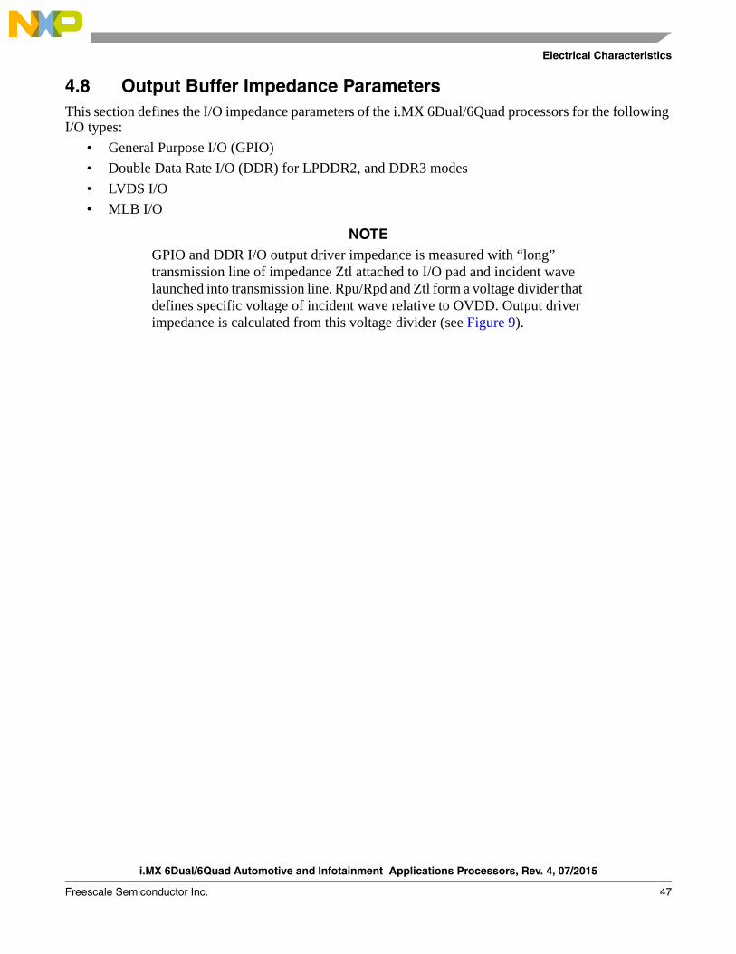
Electrical Characteristics
i.MX 6Dual/6Quad Automotive and Infotainment Applications Processors, Rev. 4, 07/2015
Freescale Semiconductor Inc. 47
4.8 Output Buffer Impedance ParametersThis section defines the I/O impedance parameters of the i.MX 6Dual/6Quad processors for the following I/O types:
• General Purpose I/O (GPIO)
• Double Data Rate I/O (DDR) for LPDDR2, and DDR3 modes
• LVDS I/O
• MLB I/O
NOTEGPIO and DDR I/O output driver impedance is measured with “long” transmission line of impedance Ztl attached to I/O pad and incident wave launched into transmission line. Rpu/Rpd and Ztl form a voltage divider that defines specific voltage of incident wave relative to OVDD. Output driver impedance is calculated from this voltage divider (see Figure 9).
i.MX 6Dual/6Quad Automotive and Infotainment Applications Processors, Rev. 4, 07/2015
48 Freescale Semiconductor Inc.
Electrical Characteristics
Figure 9. Impedance Matching Load for Measurement
ipp_do
Cload = 1p
Ztl Ω, L = 20 inches
predriver
PMOS (Rpu)
NMOS (Rpd)
pad
OVDD
OVSS
t,(ns)
U,(V)
OVDD
t,(ns)0
VDDVin (do)
Vout (pad)U,(V)
Vref
Rpu = Vovdd – Vref1
Vref1× Ztl
Rpd = × ZtlVref2
Vovdd – Vref2
Vref1 Vref2
0
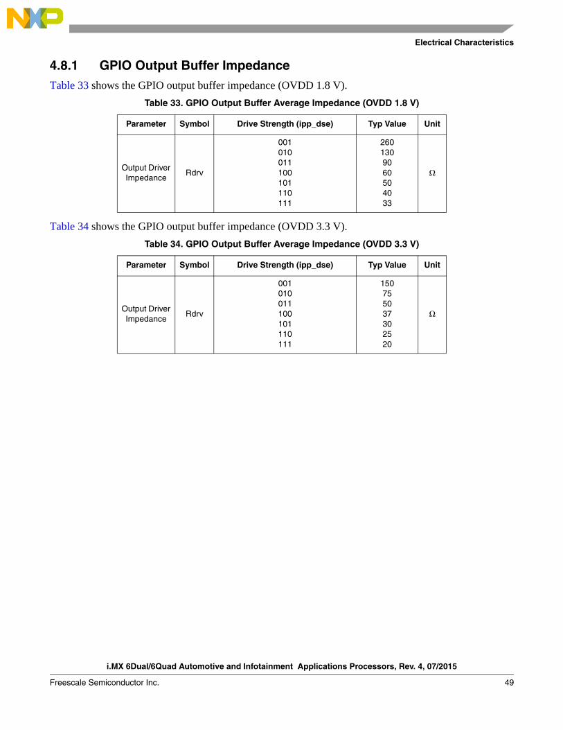
Electrical Characteristics
i.MX 6Dual/6Quad Automotive and Infotainment Applications Processors, Rev. 4, 07/2015
Freescale Semiconductor Inc. 49
4.8.1 GPIO Output Buffer ImpedanceTable 33 shows the GPIO output buffer impedance (OVDD 1.8 V).
Table 34 shows the GPIO output buffer impedance (OVDD 3.3 V).
Table 33. GPIO Output Buffer Average Impedance (OVDD 1.8 V)
Parameter Symbol Drive Strength (ipp_dse) Typ Value Unit
Output Driver Impedance
Rdrv
001010011100101110111
2601309060504033
Ω
Table 34. GPIO Output Buffer Average Impedance (OVDD 3.3 V)
Parameter Symbol Drive Strength (ipp_dse) Typ Value Unit
Output Driver Impedance
Rdrv
001010011100101110111
150755037302520
Ω
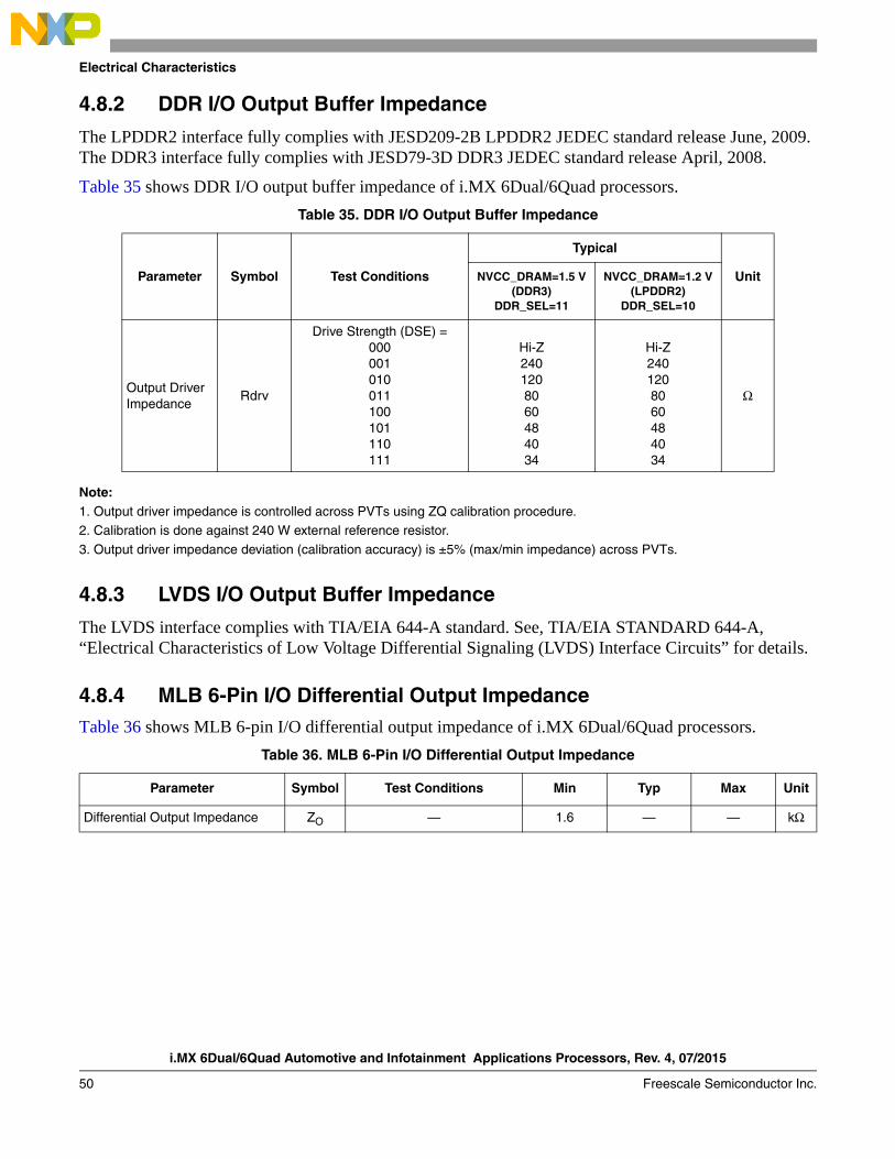
i.MX 6Dual/6Quad Automotive and Infotainment Applications Processors, Rev. 4, 07/2015
50 Freescale Semiconductor Inc.
Electrical Characteristics
4.8.2 DDR I/O Output Buffer Impedance
The LPDDR2 interface fully complies with JESD209-2B LPDDR2 JEDEC standard release June, 2009. The DDR3 interface fully complies with JESD79-3D DDR3 JEDEC standard release April, 2008.
Table 35 shows DDR I/O output buffer impedance of i.MX 6Dual/6Quad processors.
Note: 1. Output driver impedance is controlled across PVTs using ZQ calibration procedure.2. Calibration is done against 240 W external reference resistor.
3. Output driver impedance deviation (calibration accuracy) is ±5% (max/min impedance) across PVTs.
4.8.3 LVDS I/O Output Buffer Impedance
The LVDS interface complies with TIA/EIA 644-A standard. See, TIA/EIA STANDARD 644-A, “Electrical Characteristics of Low Voltage Differential Signaling (LVDS) Interface Circuits” for details.
4.8.4 MLB 6-Pin I/O Differential Output ImpedanceTable 36 shows MLB 6-pin I/O differential output impedance of i.MX 6Dual/6Quad processors.
Table 35. DDR I/O Output Buffer Impedance
Parameter Symbol Test Conditions
Typical
UnitNVCC_DRAM=1.5 V (DDR3)
DDR_SEL=11
NVCC_DRAM=1.2 V (LPDDR2)
DDR_SEL=10
Output Driver Impedance
Rdrv
Drive Strength (DSE) =000001010011100101110111
Hi-Z2401208060484034
Hi-Z2401208060484034
Ω
Table 36. MLB 6-Pin I/O Differential Output Impedance
Parameter Symbol Test Conditions Min Typ Max Unit
Differential Output Impedance ZO — 1.6 — — kΩ
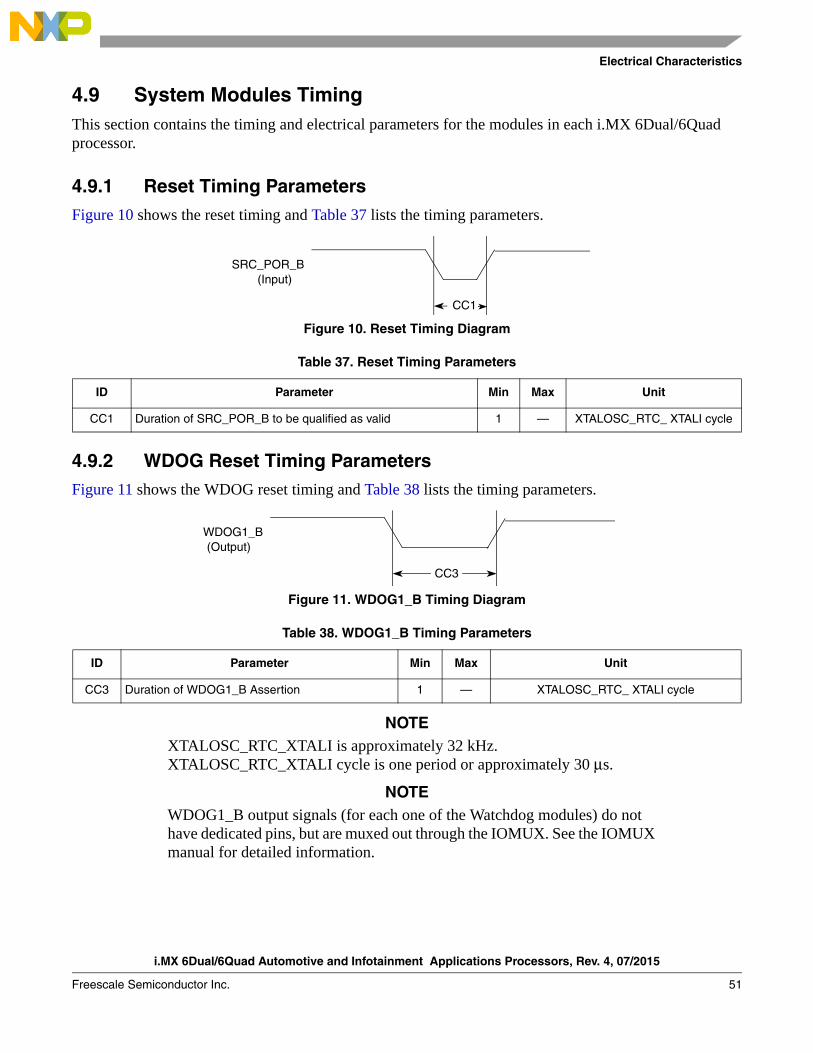
Electrical Characteristics
i.MX 6Dual/6Quad Automotive and Infotainment Applications Processors, Rev. 4, 07/2015
Freescale Semiconductor Inc. 51
4.9 System Modules TimingThis section contains the timing and electrical parameters for the modules in each i.MX 6Dual/6Quad processor.
4.9.1 Reset Timing ParametersFigure 10 shows the reset timing and Table 37 lists the timing parameters.
Figure 10. Reset Timing Diagram
4.9.2 WDOG Reset Timing ParametersFigure 11 shows the WDOG reset timing and Table 38 lists the timing parameters.
Figure 11. WDOG1_B Timing Diagram
NOTEXTALOSC_RTC_XTALI is approximately 32 kHz. XTALOSC_RTC_XTALI cycle is one period or approximately 30 μs.
NOTEWDOG1_B output signals (for each one of the Watchdog modules) do not have dedicated pins, but are muxed out through the IOMUX. See the IOMUX manual for detailed information.
Table 37. Reset Timing Parameters
ID Parameter Min Max Unit
CC1 Duration of SRC_POR_B to be qualified as valid 1 — XTALOSC_RTC_ XTALI cycle
Table 38. WDOG1_B Timing Parameters
ID Parameter Min Max Unit
CC3 Duration of WDOG1_B Assertion 1 — XTALOSC_RTC_ XTALI cycle
SRC_POR_B
CC1
(Input)
WDOG1_B
CC3
(Output)
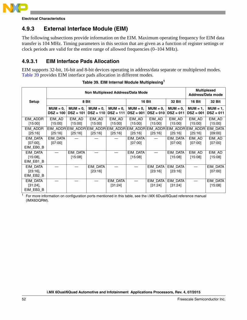
i.MX 6Dual/6Quad Automotive and Infotainment Applications Processors, Rev. 4, 07/2015
52 Freescale Semiconductor Inc.
Electrical Characteristics
4.9.3 External Interface Module (EIM)
The following subsections provide information on the EIM. Maximum operating frequency for EIM data transfer is 104 MHz. Timing parameters in this section that are given as a function of register settings or clock periods are valid for the entire range of allowed frequencies (0–104 MHz).
4.9.3.1 EIM Interface Pads Allocation
EIM supports 32-bit, 16-bit and 8-bit devices operating in address/data separate or multiplexed modes. Table 39 provides EIM interface pads allocation in different modes.
Table 39. EIM Internal Module Multiplexing1
1 For more information on configuration ports mentioned in this table, see the i.MX 6Dual/6Quad reference manual (IMX6DQRM).
Setup
Non Multiplexed Address/Data ModeMultiplexed
Address/Data mode
8 Bit 16 Bit 32 Bit 16 Bit 32 Bit
MUM = 0, DSZ = 100
MUM = 0, DSZ = 101
MUM = 0, DSZ = 110
MUM = 0, DSZ = 111
MUM = 0, DSZ = 001
MUM = 0, DSZ = 010
MUM = 0, DSZ = 011
MUM = 1,DSZ = 001
MUM = 1,DSZ = 011
EIM_ADDR[15:00]
EIM_AD[15:00]
EIM_AD[15:00]
EIM_AD [15:00]
EIM_AD[15:00]
EIM_AD[15:00]
EIM_AD[15:00]
EIM_AD [15:00]
EIM_AD [15:00]
EIM_AD [15:00]
EIM_ADDR[25:16]
EIM_ADDR[25:16]
EIM_ADDR[25:16]
EIM_ADDR[25:16]
EIM_ADDR[25:16]
EIM_ADDR[25:16]
EIM_ADDR[25:16]
EIM_ADDR[25:16]
EIM_ADDR[25:16]
EIM_DATA[09:00]
EIM_DATA[07:00],
EIM_EB0_B
EIM_DATA[07:00]
— — — EIM_DATA[07:00]
— EIM_DATA[07:00]
EIM_AD [07:00]
EIM_AD [07:00]
EIM_DATA[15:08],
EIM_EB1_B
— EIM_DATA[15:08]
— — EIM_DATA[15:08]
— EIM_DATA[15:08]
EIM_AD [15:08]
EIM_AD[15:08]
EIM_DATA[23:16],
EIM_EB2_B
— — EIM_DATA[23:16]
— — EIM_DATA [23:16]
EIM_DATA[23:16]
— EIM_DATA[07:00]
EIM_DATA[31:24],
EIM_EB3_B
— — — EIM_DATA[31:24]
— EIM_DATA [31:24]
EIM_DATA[31:24]
— EIM_DATA[15:08]
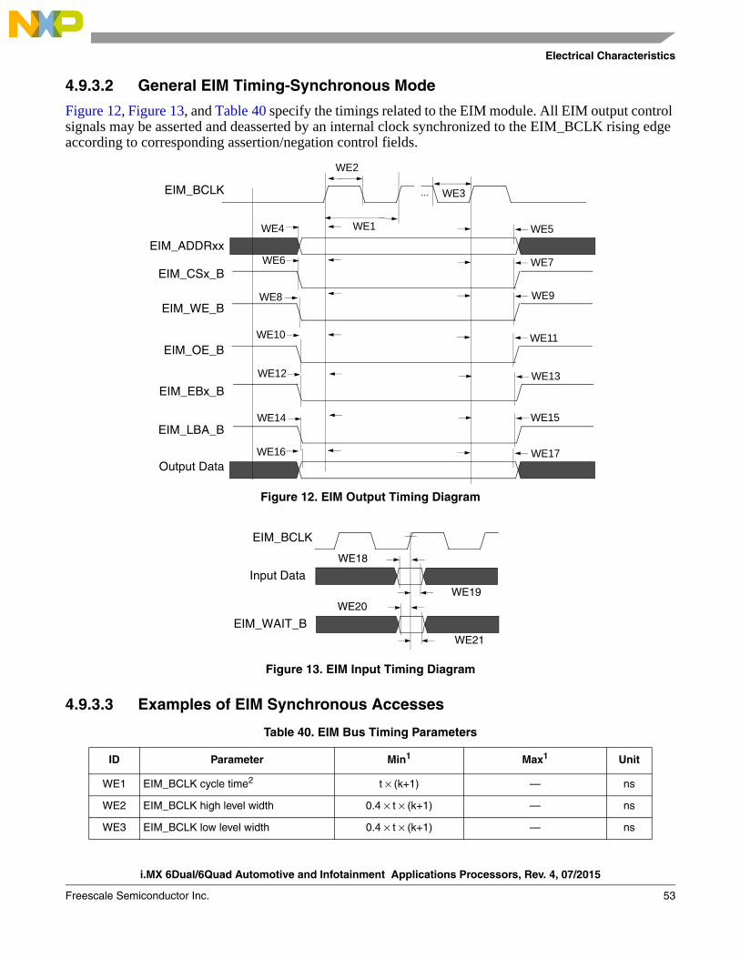
Electrical Characteristics
i.MX 6Dual/6Quad Automotive and Infotainment Applications Processors, Rev. 4, 07/2015
Freescale Semiconductor Inc. 53
4.9.3.2 General EIM Timing-Synchronous Mode
Figure 12, Figure 13, and Table 40 specify the timings related to the EIM module. All EIM output control signals may be asserted and deasserted by an internal clock synchronized to the EIM_BCLK rising edge according to corresponding assertion/negation control fields.
Figure 12. EIM Output Timing Diagram
Figure 13. EIM Input Timing Diagram
4.9.3.3 Examples of EIM Synchronous Accesses
Table 40. EIM Bus Timing Parameters
ID Parameter Min1 Max1 Unit
WE1 EIM_BCLK cycle time2 t × (k+1) — ns
WE2 EIM_BCLK high level width 0.4 × t × (k+1) — ns
WE3 EIM_BCLK low level width 0.4 × t × (k+1) — ns
WE4
EIM_ADDRxx
EIM_CSx_B
EIM_WE_B
EIM_OE_B
EIM_BCLK
EIM_EBx_B
EIM_LBA_B
Output Data
...
WE5
WE6 WE7
WE8 WE9
WE10 WE11
WE12 WE13
WE14 WE15
WE16 WE17
WE3
WE2
WE1
Input Data
EIM_WAIT_B
EIM_BCLK
WE19
WE18
WE21
WE20
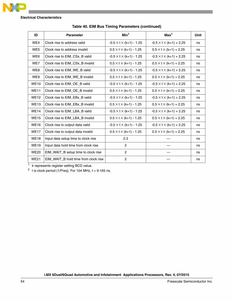
i.MX 6Dual/6Quad Automotive and Infotainment Applications Processors, Rev. 4, 07/2015
54 Freescale Semiconductor Inc.
Electrical Characteristics
WE4 Clock rise to address valid -0.5 × t × (k+1) - 1.25 -0.5 × t × (k+1) + 2.25 ns
WE5 Clock rise to address invalid 0.5 × t × (k+1) - 1.25 0.5 × t × (k+1) + 2.25 ns
WE6 Clock rise to EIM_CSx_B valid -0.5 × t × (k+1) - 1.25 -0.5 × t × (k+1) + 2.25 ns
WE7 Clock rise to EIM_CSx_B invalid 0.5 × t × (k+1) - 1.25 0.5 × t × (k+1) + 2.25 ns
WE8 Clock rise to EIM_WE_B valid -0.5 × t × (k+1) - 1.25 -0.5 × t × (k+1) + 2.25 ns
WE9 Clock rise to EIM_WE_B invalid 0.5 × t × (k+1) - 1.25 0.5 × t × (k+1) + 2.25 ns
WE10 Clock rise to EIM_OE_B valid -0.5 × t × (k+1) - 1.25 -0.5 × t × (k+1) + 2.25 ns
WE11 Clock rise to EIM_OE_B invalid 0.5 × t × (k+1) - 1.25 0.5 × t × (k+1) + 2.25 ns
WE12 Clock rise to EIM_EBx_B valid -0.5 × t × (k+1) - 1.25 -0.5 × t × (k+1) + 2.25 ns
WE13 Clock rise to EIM_EBx_B invalid 0.5 × t × (k+1) - 1.25 0.5 × t × (k+1) + 2.25 ns
WE14 Clock rise to EIM_LBA_B valid -0.5 × t × (k+1) - 1.25 -0.5 × t × (k+1) + 2.25 ns
WE15 Clock rise to EIM_LBA_B invalid 0.5 × t × (k+1) - 1.25 0.5 × t × (k+1) + 2.25 ns
WE16 Clock rise to output data valid -0.5 × t × (k+1) - 1.25 -0.5 × t × (k+1) + 2.25 ns
WE17 Clock rise to output data invalid 0.5 × t × (k+1) - 1.25 0.5 × t × (k+1) + 2.25 ns
WE18 Input data setup time to clock rise 2.3 — ns
WE19 Input data hold time from clock rise 2 — ns
WE20 EIM_WAIT_B setup time to clock rise 2 — ns
WE21 EIM_WAIT_B hold time from clock rise 2 — ns
1 k represents register setting BCD value.2 t is clock period (1/Freq). For 104 MHz, t = 9.165 ns.
Table 40. EIM Bus Timing Parameters (continued)
ID Parameter Min1 Max1 Unit
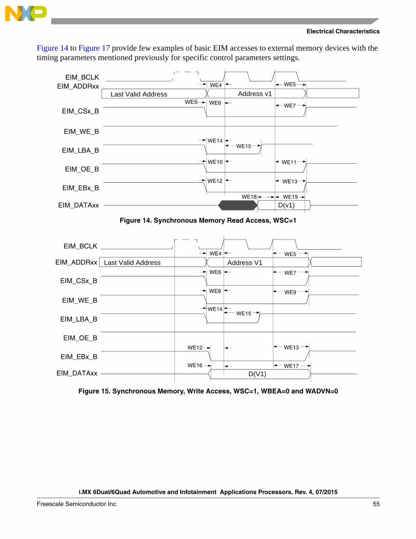
Electrical Characteristics
i.MX 6Dual/6Quad Automotive and Infotainment Applications Processors, Rev. 4, 07/2015
Freescale Semiconductor Inc. 55
Figure 14 to Figure 17 provide few examples of basic EIM accesses to external memory devices with the timing parameters mentioned previously for specific control parameters settings.
Figure 14. Synchronous Memory Read Access, WSC=1
Figure 15. Synchronous Memory, Write Access, WSC=1, WBEA=0 and WADVN=0
Last Valid Address Address v1
D(v1)
EIM_BCLKEIM_ADDRxx
EIM_DATAxx
EIM_WE_B
EIM_LBA_B
EIM_OE_B
EIM_EBx_B
EIM_CSx_B
WE4 WE5
WE6WE7
WE11
WE13WE12
WE14WE15
WE18 WE19
WE6
WE10
Last Valid Address Address V1
D(V1)
EIM_BCLK
EIM_ADDRxx
EIM_DATAxx
EIM_WE_B
EIM_LBA_B
EIM_OE_B
EIM_EBx_B
EIM_CSx_B
WE4 WE5
WE6 WE7
WE8 WE9
WE12 WE13
WE14WE15
WE16 WE17
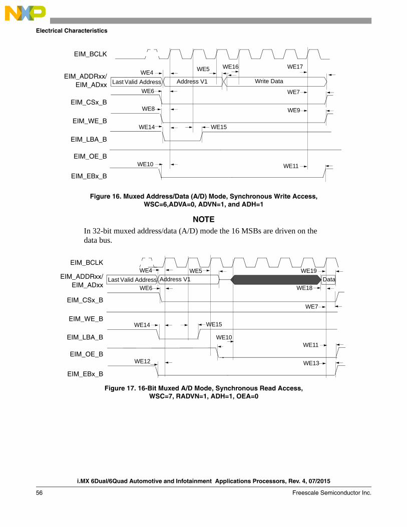
i.MX 6Dual/6Quad Automotive and Infotainment Applications Processors, Rev. 4, 07/2015
56 Freescale Semiconductor Inc.
Electrical Characteristics
Figure 16. Muxed Address/Data (A/D) Mode, Synchronous Write Access, WSC=6,ADVA=0, ADVN=1, and ADH=1
NOTEIn 32-bit muxed address/data (A/D) mode the 16 MSBs are driven on the data bus.
Figure 17. 16-Bit Muxed A/D Mode, Synchronous Read Access, WSC=7, RADVN=1, ADH=1, OEA=0
EIM_BCLK
EIM_ADDRxx/
EIM_WE_B
EIM_LBA_B
EIM_OE_B
EIM_EBx_B
EIM_CSx_B
Address V1 Write DataEIM_ADxx
WE4WE16
WE6 WE7
WE9WE8
WE10 WE11
WE14 WE15
WE17WE5
Last AddressValid
Last
EIM_BCLK
EIM_ADDRxx/
EIM_WE_B
EIM_LBA_B
EIM_OE_B
EIM_EBx_B
EIM_CSx_B
Address V1 DataAddressEIM_ADxx
WE5
WE6
WE7
WE14 WE15
WE10WE11
WE12 WE13
WE18
WE19WE4
Valid
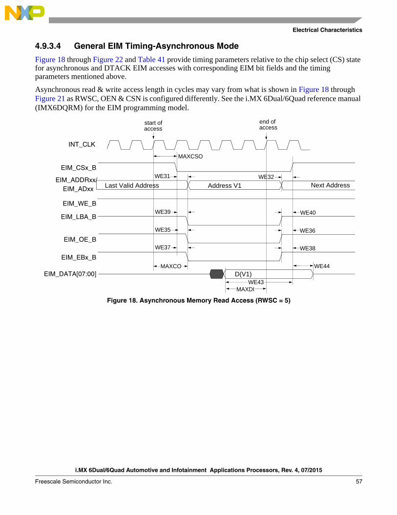
Electrical Characteristics
i.MX 6Dual/6Quad Automotive and Infotainment Applications Processors, Rev. 4, 07/2015
Freescale Semiconductor Inc. 57
4.9.3.4 General EIM Timing-Asynchronous Mode
Figure 18 through Figure 22 and Table 41 provide timing parameters relative to the chip select (CS) state for asynchronous and DTACK EIM accesses with corresponding EIM bit fields and the timing parameters mentioned above.
Asynchronous read & write access length in cycles may vary from what is shown in Figure 18 through Figure 21 as RWSC, OEN & CSN is configured differently. See the i.MX 6Dual/6Quad reference manual (IMX6DQRM) for the EIM programming model.
Figure 18. Asynchronous Memory Read Access (RWSC = 5)
Last Valid Address Address V1
D(V1)
EIM_ADDRxx/
EIM_DATA[07:00]
EIM_WE_B
EIM_LBA_B
EIM_OE_B
EIM_EBx_B
EIM_CSx_B
Next Address
WE39
WE35
WE37
WE32
WE36
WE38
WE43
WE40
WE31
WE44
INT_CLK
start ofaccess
end ofaccess
MAXDI
MAXCSO
MAXCO
EIM_ADxx
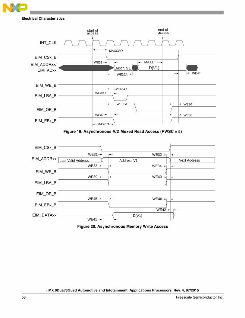
i.MX 6Dual/6Quad Automotive and Infotainment Applications Processors, Rev. 4, 07/2015
58 Freescale Semiconductor Inc.
Electrical Characteristics
Figure 19. Asynchronous A/D Muxed Read Access (RWSC = 5)
Figure 20. Asynchronous Memory Write Access
Addr. V1 D(V1)EIM_ADDRxx/
EIM_WE_B
EIM_LBA_B
EIM_OE_B
EIM_EBx_B
EIM_CSx_B
WE39
WE35A
WE37
WE36
WE38
WE40A
WE31
WE44
INT_CLK
start ofaccess
end ofaccess
MAXDI
MAXCSO
MAXCO
WE32AEIM_ADxx
Last Valid Address Address V1
D(V1)
EIM_ADDRxx
EIM_DATAxx
EIM_WE_B
EIM_LBA_B
EIM_OE_B
EIM_EBx_B
EIM_CSx_B
Next Address
WE31
WE39
WE33
WE45
WE32
WE40
WE34
WE46
WE42
WE41
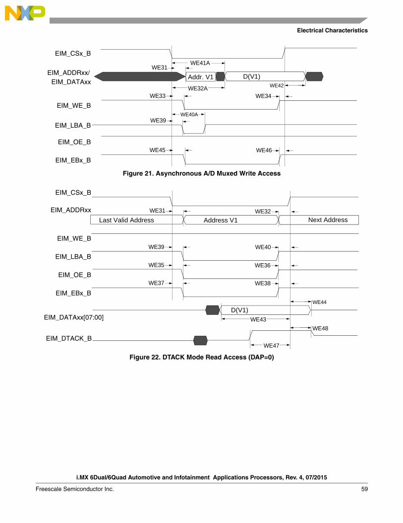
Electrical Characteristics
i.MX 6Dual/6Quad Automotive and Infotainment Applications Processors, Rev. 4, 07/2015
Freescale Semiconductor Inc. 59
Figure 21. Asynchronous A/D Muxed Write Access
Figure 22. DTACK Mode Read Access (DAP=0)
EIM_WE_B
EIM_OE_B
EIM_EBx_B
EIM_CSx_B
WE33
WE45
WE34
WE46
Addr. V1 D(V1)EIM_ADDRxx/
WE31
WE42
WE41A
WE32AEIM_DATAxx
EIM_LBA_BWE39
WE40A
Last Valid Address Address V1
D(V1)
EIM_ADDRxx
EIM_DATAxx[07:00]
EIM_WE_B
EIM_LBA_B
EIM_OE_B
EIM_EBx_B
EIM_CSx_B
Next Address
WE39
WE35
WE37
WE32
WE36
WE38
WE43
WE40
WE31
WE44
WE47
WE48
EIM_DTACK_B
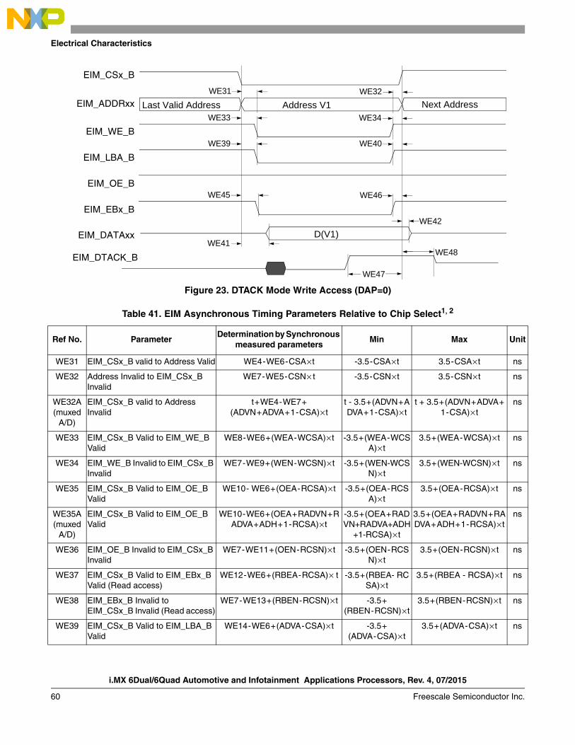
i.MX 6Dual/6Quad Automotive and Infotainment Applications Processors, Rev. 4, 07/2015
60 Freescale Semiconductor Inc.
Electrical Characteristics
Figure 23. DTACK Mode Write Access (DAP=0)
Table 41. EIM Asynchronous Timing Parameters Relative to Chip Select1, 2
Ref No. ParameterDetermination by Synchronous
measured parametersMin Max Unit
WE31 EIM_CSx_B valid to Address Valid WE4-WE6-CSA×t -3.5-CSA×t 3.5-CSA× t ns
WE32 Address Invalid to EIM_CSx_B Invalid
WE7-WE5-CSN× t -3.5-CSN×t 3.5-CSN× t ns
WE32A(muxed
A/D)
EIM_CSx_B valid to Address Invalid
t+WE4-WE7+(ADVN+ADVA+1-CSA)× t
t - 3.5+(ADVN+ADVA+1-CSA)× t
t + 3.5+(ADVN+ADVA+1-CSA)× t
ns
WE33 EIM_CSx_B Valid to EIM_WE_B Valid
WE8-WE6+(WEA-WCSA)× t -3.5+(WEA-WCSA)× t
3.5+(WEA-WCSA)×t ns
WE34 EIM_WE_B Invalid to EIM_CSx_B Invalid
WE7-WE9+(WEN-WCSN)× t -3.5+(WEN-WCSN)× t
3.5+(WEN-WCSN)×t ns
WE35 EIM_CSx_B Valid to EIM_OE_B Valid
WE10- WE6+(OEA-RCSA)× t -3.5+(OEA-RCSA)× t
3.5+(OEA-RCSA)×t ns
WE35A(muxed
A/D)
EIM_CSx_B Valid to EIM_OE_B Valid
WE10-WE6+(OEA+RADVN+RADVA+ADH+1-RCSA)×t
-3.5+(OEA+RADVN+RADVA+ADH
+1-RCSA)× t
3.5+(OEA+RADVN+RADVA+ADH+1-RCSA)× t
ns
WE36 EIM_OE_B Invalid to EIM_CSx_B Invalid
WE7-WE11+(OEN-RCSN)× t -3.5+(OEN-RCSN)× t
3.5+(OEN-RCSN)× t ns
WE37 EIM_CSx_B Valid to EIM_EBx_B Valid (Read access)
WE12-WE6+(RBEA-RCSA)× t -3.5+(RBEA- RCSA)× t
3.5+(RBEA - RCSA)×t ns
WE38 EIM_EBx_B Invalid to EIM_CSx_B Invalid (Read access)
WE7-WE13+(RBEN-RCSN)×t -3.5+(RBEN-RCSN)×t
3.5+(RBEN-RCSN)×t ns
WE39 EIM_CSx_B Valid to EIM_LBA_B Valid
WE14-WE6+(ADVA-CSA)× t -3.5+(ADVA-CSA)× t
3.5+(ADVA-CSA)× t ns
Last Valid Address Address V1
D(V1)
EIM_ADDRxx
EIM_DATAxx
EIM_WE_B
EIM_LBA_B
EIM_OE_B
EIM_EBx_B
EIM_CSx_B
Next Address
WE31
WE39
WE33
WE45
WE32
WE40
WE34
WE46
WE42
WE41
EIM_DTACK_B
WE47
WE48
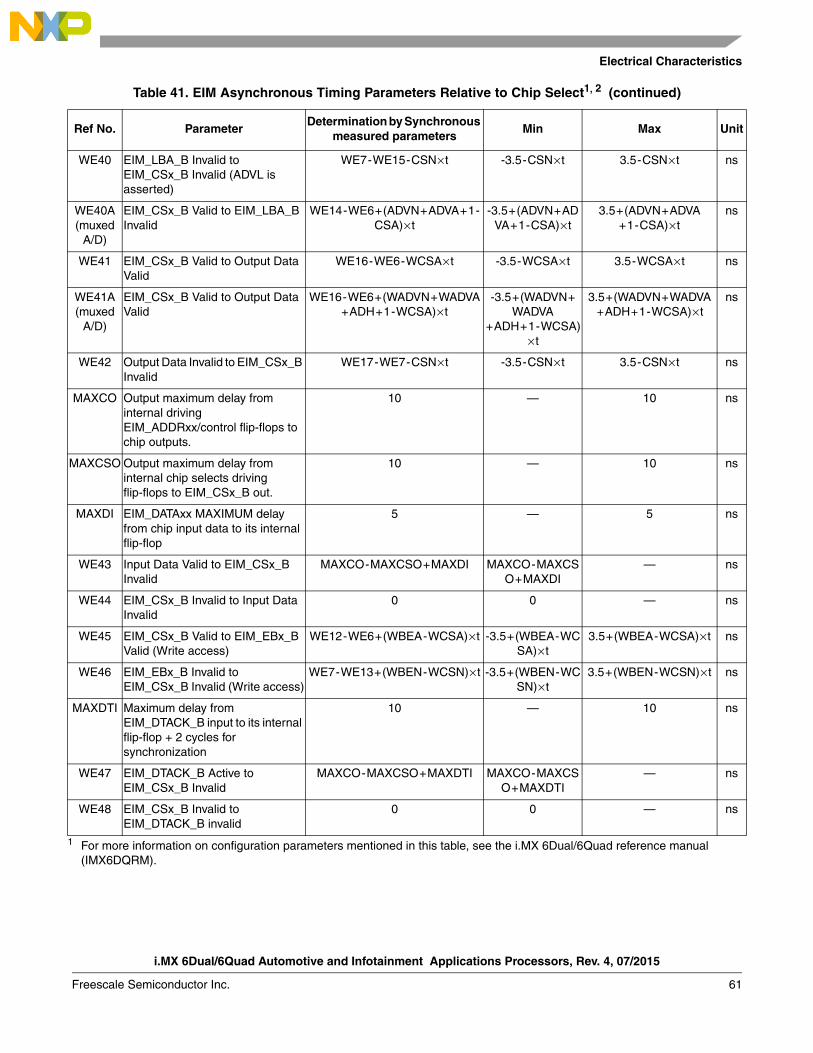
Electrical Characteristics
i.MX 6Dual/6Quad Automotive and Infotainment Applications Processors, Rev. 4, 07/2015
Freescale Semiconductor Inc. 61
WE40 EIM_LBA_B Invalid to EIM_CSx_B Invalid (ADVL is asserted)
WE7-WE15-CSN× t -3.5-CSN×t 3.5-CSN× t ns
WE40A(muxed
A/D)
EIM_CSx_B Valid to EIM_LBA_B Invalid
WE14-WE6+(ADVN+ADVA+1-CSA)× t
-3.5+(ADVN+ADVA+1-CSA)× t
3.5+(ADVN+ADVA+1-CSA)×t
ns
WE41 EIM_CSx_B Valid to Output Data Valid
WE16-WE6-WCSA× t -3.5-WCSA× t 3.5-WCSA× t ns
WE41A(muxed
A/D)
EIM_CSx_B Valid to Output Data Valid
WE16-WE6+(WADVN+WADVA+ADH+1-WCSA)× t
-3.5+(WADVN+WADVA
+ADH+1-WCSA)× t
3.5+(WADVN+WADVA+ADH+1-WCSA)× t
ns
WE42 Output Data Invalid to EIM_CSx_B Invalid
WE17-WE7-CSN× t -3.5-CSN×t 3.5-CSN× t ns
MAXCO Output maximum delay from internal driving EIM_ADDRxx/control flip-flops to chip outputs.
10 — 10 ns
MAXCSO Output maximum delay from internal chip selects driving flip-flops to EIM_CSx_B out.
10 — 10 ns
MAXDI EIM_DATAxx MAXIMUM delay from chip input data to its internal flip-flop
5 — 5 ns
WE43 Input Data Valid to EIM_CSx_B Invalid
MAXCO-MAXCSO+MAXDI MAXCO-MAXCSO+MAXDI
— ns
WE44 EIM_CSx_B Invalid to Input Data Invalid
0 0 — ns
WE45 EIM_CSx_B Valid to EIM_EBx_B Valid (Write access)
WE12-WE6+(WBEA-WCSA)×t -3.5+(WBEA-WCSA)× t
3.5+(WBEA-WCSA)×t ns
WE46 EIM_EBx_B Invalid to EIM_CSx_B Invalid (Write access)
WE7-WE13+(WBEN-WCSN)× t -3.5+(WBEN-WCSN)× t
3.5+(WBEN-WCSN)× t ns
MAXDTI Maximum delay fromEIM_DTACK_B input to its internal flip-flop + 2 cycles for synchronization
10 — 10 ns
WE47 EIM_DTACK_B Active to EIM_CSx_B Invalid
MAXCO-MAXCSO+MAXDTI MAXCO-MAXCSO+MAXDTI
— ns
WE48 EIM_CSx_B Invalid to EIM_DTACK_B invalid
0 0 — ns
1 For more information on configuration parameters mentioned in this table, see the i.MX 6Dual/6Quad reference manual (IMX6DQRM).
Table 41. EIM Asynchronous Timing Parameters Relative to Chip Select1, 2 (continued)
Ref No. ParameterDetermination by Synchronous
measured parametersMin Max Unit
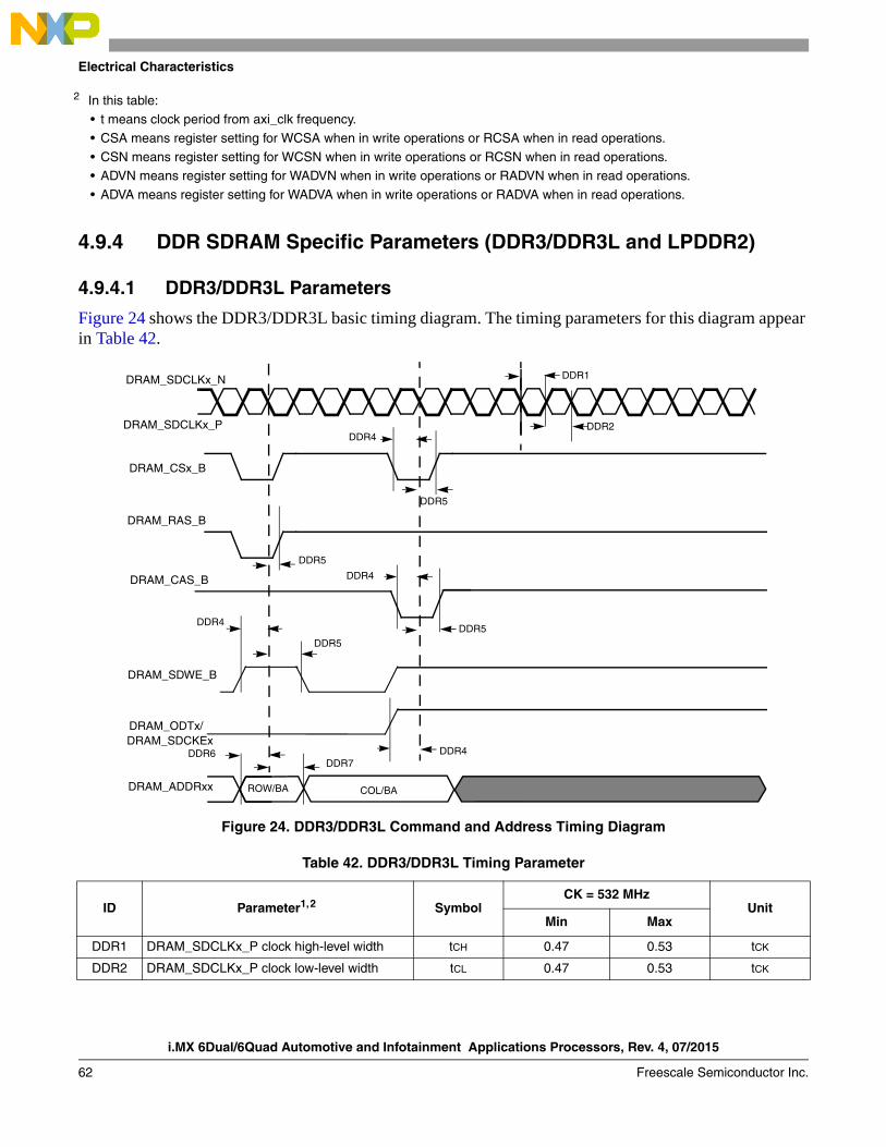
i.MX 6Dual/6Quad Automotive and Infotainment Applications Processors, Rev. 4, 07/2015
62 Freescale Semiconductor Inc.
Electrical Characteristics
4.9.4 DDR SDRAM Specific Parameters (DDR3/DDR3L and LPDDR2)
4.9.4.1 DDR3/DDR3L Parameters
Figure 24 shows the DDR3/DDR3L basic timing diagram. The timing parameters for this diagram appear in Table 42.
Figure 24. DDR3/DDR3L Command and Address Timing Diagram
2 In this table:• t means clock period from axi_clk frequency.
• CSA means register setting for WCSA when in write operations or RCSA when in read operations.
• CSN means register setting for WCSN when in write operations or RCSN when in read operations.• ADVN means register setting for WADVN when in write operations or RADVN when in read operations.
• ADVA means register setting for WADVA when in write operations or RADVA when in read operations.
Table 42. DDR3/DDR3L Timing Parameter
ID Parameter1,2 SymbolCK = 532 MHz
UnitMin Max
DDR1 DRAM_SDCLKx_P clock high-level width tCH 0.47 0.53 tCK
DDR2 DRAM_SDCLKx_P clock low-level width tCL 0.47 0.53 tCK
DRAM_SDCLKx_P
DRAM_SDWE_B
DRAM_ADDRxx ROW/BA COL/BA
DRAM_CSx_B
DRAM_CAS_B
DRAM_RAS_B
DDR1
DDR2DDR4
DDR4
DDR4
DDR5
DDR5
DDR5DDR5
DDR6DDR7
DRAM_SDCLKx_N
DRAM_ODTx/
DDR4DRAM_SDCKEx
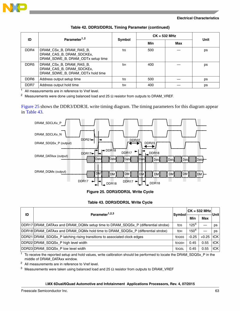
Electrical Characteristics
i.MX 6Dual/6Quad Automotive and Infotainment Applications Processors, Rev. 4, 07/2015
Freescale Semiconductor Inc. 63
Figure 25 shows the DDR3/DDR3L write timing diagram. The timing parameters for this diagram appear in Table 43.
Figure 25. DDR3/DDR3L Write Cycle
DDR4 DRAM_CSx_B, DRAM_RAS_B, DRAM_CAS_B, DRAM_SDCKEx, DRAM_SDWE_B, DRAM_ODTx setup time
tIS 500 — ps
DDR5 DRAM_CSx_B, DRAM_RAS_B, DRAM_CAS_B, DRAM_SDCKEx, DRAM_SDWE_B, DRAM_ODTx hold time
tIH 400 — ps
DDR6 Address output setup time tIS 500 — ps
DDR7 Address output hold time tIH 400 — ps1 All measurements are in reference to Vref level.2 Measurements were done using balanced load and 25 Ω resistor from outputs to DRAM_VREF.
Table 43. DDR3/DDR3L Write Cycle
ID Parameter1,2,3
1 To receive the reported setup and hold values, write calibration should be performed to locate the DRAM_SDQSx_P in the middle of DRAM_DATAxx window.
2 All measurements are in reference to Vref level.3 Measurements were taken using balanced load and 25 Ω resistor from outputs to DRAM_VREF
SymbolCK = 532 MHz
UnitMin Max
DDR17 DRAM_DATAxx and DRAM_DQMx setup time to DRAM_SDQSx_P (differential strobe) tDS 1254 — ps
DDR18 DRAM_DATAxx and DRAM_DQMx hold time to DRAM_SDQSx_P (differential strobe) tDH 1504 — ps
DDR21 DRAM_SDQSx_P latching rising transitions to associated clock edges tDQSS -0.25 +0.25 tCK
DDR22 DRAM_SDQSx_P high level width tDQSH 0.45 0.55 tCK
DDR23 DRAM_SDQSx_P low level width tDQSL 0.45 0.55 tCK
Table 42. DDR3/DDR3L Timing Parameter (continued)
ID Parameter1,2 SymbolCK = 532 MHz
UnitMin Max
DRAM_SDCLKx_P
DRAM_SDCLKx_N
DRAM_SDQSx_P (output)
DRAM_DATAxx (output)
DRAM_DQMx (output)
Data Data Data Data Data Data Data Data
DM DM DM DM DM DM DM DM
DDR17
DDR17
DDR17
DDR17
DDR18DDR18
DDR18 DDR18
DDR21DDR23
DDR22
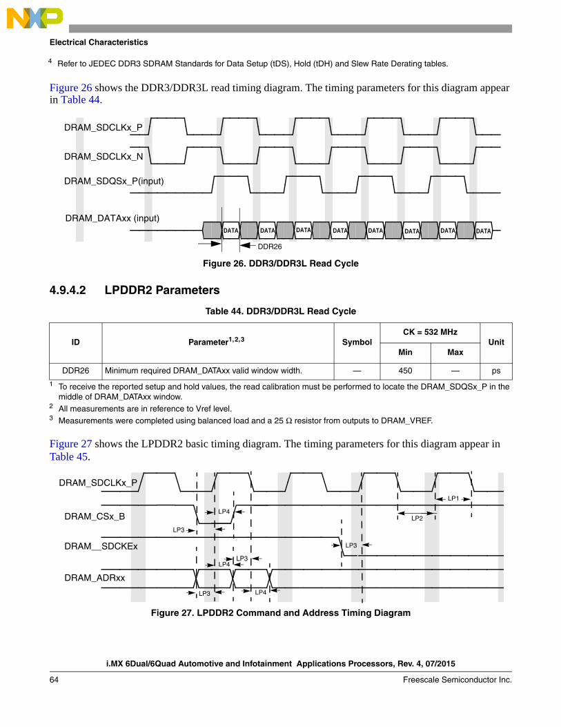
i.MX 6Dual/6Quad Automotive and Infotainment Applications Processors, Rev. 4, 07/2015
64 Freescale Semiconductor Inc.
Electrical Characteristics
Figure 26 shows the DDR3/DDR3L read timing diagram. The timing parameters for this diagram appear in Table 44.
Figure 26. DDR3/DDR3L Read Cycle
4.9.4.2 LPDDR2 Parameters
Figure 27 shows the LPDDR2 basic timing diagram. The timing parameters for this diagram appear in Table 45.
Figure 27. LPDDR2 Command and Address Timing Diagram
4 Refer to JEDEC DDR3 SDRAM Standards for Data Setup (tDS), Hold (tDH) and Slew Rate Derating tables.
Table 44. DDR3/DDR3L Read Cycle
ID Parameter1,2,3
1 To receive the reported setup and hold values, the read calibration must be performed to locate the DRAM_SDQSx_P in the middle of DRAM_DATAxx window.
2 All measurements are in reference to Vref level.3 Measurements were completed using balanced load and a 25 Ω resistor from outputs to DRAM_VREF.
SymbolCK = 532 MHz
UnitMin Max
DDR26 Minimum required DRAM_DATAxx valid window width. — 450 — ps
DRAM_SDCLKx_P
DRAM_SDCLKx_N
DRAM_SDQSx_P(input)
DRAM_DATAxx (input)DATADATADATADATADATADATADATADATA
DDR26
DRAM_SDCLKx_P
DRAM_CSx_B
DRAM__SDCKEx
DRAM_ADRxx
LP4
LP4
LP3LP4
LP3
LP2
LP3
LP1
LP3
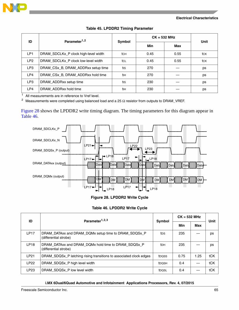
Electrical Characteristics
i.MX 6Dual/6Quad Automotive and Infotainment Applications Processors, Rev. 4, 07/2015
Freescale Semiconductor Inc. 65
Figure 28 shows the LPDDR2 write timing diagram. The timing parameters for this diagram appear in Table 46.
Figure 28. LPDDR2 Write Cycle
Table 45. LPDDR2 Timing Parameter
ID Parameter1,2
1 All measurements are in reference to Vref level.2 Measurements were completed using balanced load and a 25 Ω resistor from outputs to DRAM_VREF.
SymbolCK = 532 MHz
UnitMin Max
LP1 DRAM_SDCLKx_P clock high-level width tCH 0.45 0.55 tCK
LP2 DRAM_SDCLKx_P clock low-level width tCL 0.45 0.55 tCK
LP3 DRAM_CSx_B, DRAM_ADDRxx setup time tIS 270 — ps
LP4 DRAM_CSx_B, DRAM_ADDRxx hold time tIH 270 — ps
LP3 DRAM_ADDRxx setup time tIS 230 — ps
LP4 DRAM_ADDRxx hold time tIH 230 — ps
Table 46. LPDDR2 Write Cycle
ID Parameter1,2,3 SymbolCK = 532 MHz
UnitMin Max
LP17 DRAM_DATAxx and DRAM_DQMx setup time to DRAM_SDQSx_P (differential strobe)
tDS 235 — ps
LP18 DRAM_DATAxx and DRAM_DQMx hold time to DRAM_SDQSx_P (differential strobe)
tDH 235 — ps
LP21 DRAM_SDQSx_P latching rising transitions to associated clock edges tDQSS 0.75 1.25 tCK
LP22 DRAM_SDQSx_P high level width tDQSH 0.4 — tCK
LP23 DRAM_SDQSx_P low level width tDQSL 0.4 — tCK
DRAM_SDCLKx_P
DRAM_SDCLKx_N
DRAM_SDQSx_P (output)
DRAM_DATAxx (output)
DRAM_DQMx (output)
Data Data Data Data Data Data Data Data
DM DM DM DM DM DM DM DM
LP17
LP17
LP17
LP17
LP18LP18
LP18 LP18
LP21LP23
LP22
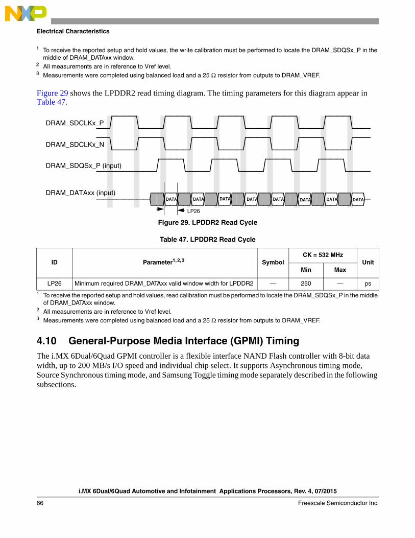
i.MX 6Dual/6Quad Automotive and Infotainment Applications Processors, Rev. 4, 07/2015
66 Freescale Semiconductor Inc.
Electrical Characteristics
Figure 29 shows the LPDDR2 read timing diagram. The timing parameters for this diagram appear in Table 47.
Figure 29. LPDDR2 Read Cycle
4.10 General-Purpose Media Interface (GPMI) TimingThe i.MX 6Dual/6Quad GPMI controller is a flexible interface NAND Flash controller with 8-bit data width, up to 200 MB/s I/O speed and individual chip select. It supports Asynchronous timing mode, Source Synchronous timing mode, and Samsung Toggle timing mode separately described in the following subsections.
1 To receive the reported setup and hold values, the write calibration must be performed to locate the DRAM_SDQSx_P in the middle of DRAM_DATAxx window.
2 All measurements are in reference to Vref level.3 Measurements were completed using balanced load and a 25 Ω resistor from outputs to DRAM_VREF.
Table 47. LPDDR2 Read Cycle
ID Parameter1,2,3
1 To receive the reported setup and hold values, read calibration must be performed to locate the DRAM_SDQSx_P in the middle of DRAM_DATAxx window.
2 All measurements are in reference to Vref level.3 Measurements were completed using balanced load and a 25 Ω resistor from outputs to DRAM_VREF.
SymbolCK = 532 MHz
UnitMin Max
LP26 Minimum required DRAM_DATAxx valid window width for LPDDR2 — 250 — ps
DRAM_SDCLKx_P
DRAM_SDCLKx_N
DRAM_SDQSx_P (input)
DRAM_DATAxx (input)DATADATADATADATADATADATADATADATA
LP26
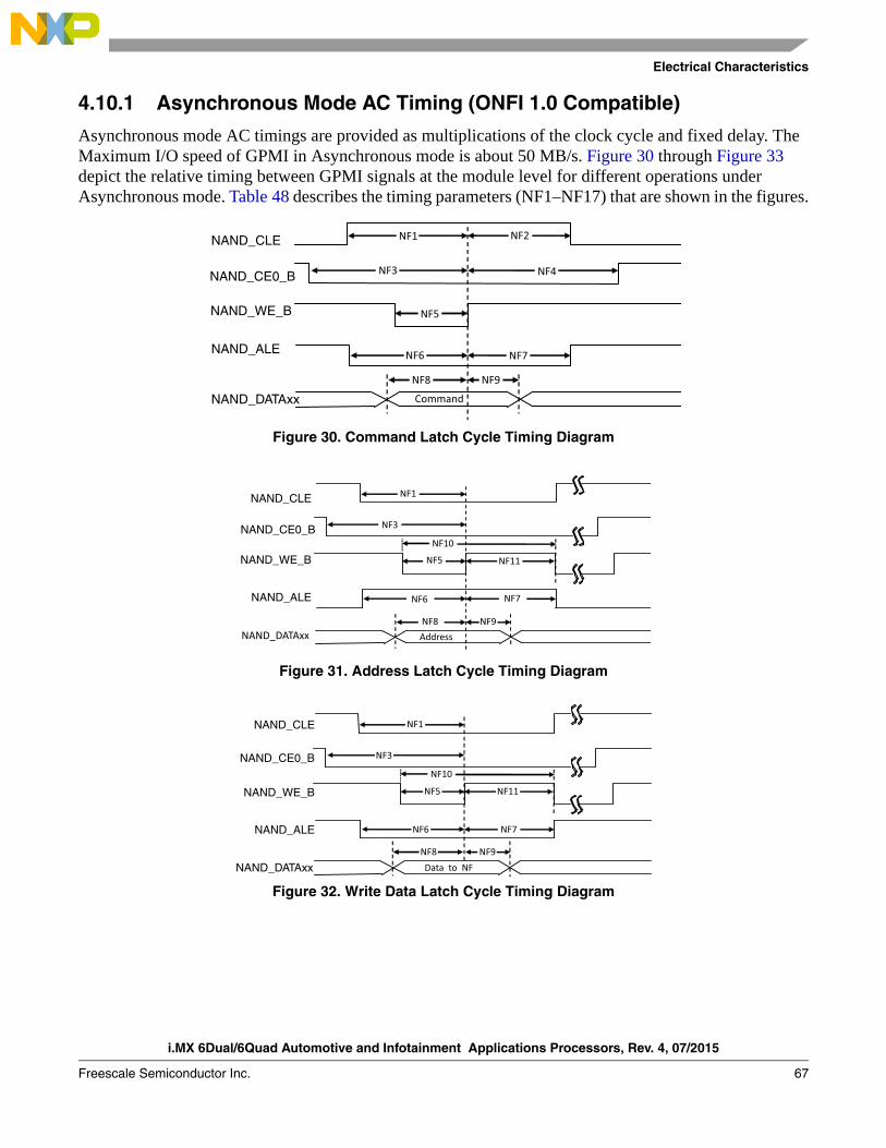
Electrical Characteristics
i.MX 6Dual/6Quad Automotive and Infotainment Applications Processors, Rev. 4, 07/2015
Freescale Semiconductor Inc. 67
4.10.1 Asynchronous Mode AC Timing (ONFI 1.0 Compatible)
Asynchronous mode AC timings are provided as multiplications of the clock cycle and fixed delay. The Maximum I/O speed of GPMI in Asynchronous mode is about 50 MB/s. Figure 30 through Figure 33 depict the relative timing between GPMI signals at the module level for different operations under Asynchronous mode. Table 48 describes the timing parameters (NF1–NF17) that are shown in the figures.
Figure 30. Command Latch Cycle Timing Diagram
Figure 31. Address Latch Cycle Timing Diagram
Figure 32. Write Data Latch Cycle Timing Diagram
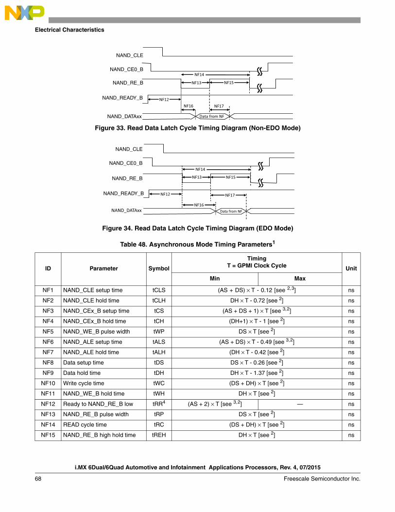
i.MX 6Dual/6Quad Automotive and Infotainment Applications Processors, Rev. 4, 07/2015
68 Freescale Semiconductor Inc.
Electrical Characteristics
Figure 33. Read Data Latch Cycle Timing Diagram (Non-EDO Mode)
Figure 34. Read Data Latch Cycle Timing Diagram (EDO Mode)
Table 48. Asynchronous Mode Timing Parameters1
ID Parameter Symbol
TimingT = GPMI Clock Cycle Unit
Min Max
NF1 NAND_CLE setup time tCLS (AS + DS) × T - 0.12 [see 2,3] ns
NF2 NAND_CLE hold time tCLH DH × T - 0.72 [see 2] ns
NF3 NAND_CEx_B setup time tCS (AS + DS + 1) × T [see 3,2] ns
NF4 NAND_CEx_B hold time tCH (DH+1) × T - 1 [see 2] ns
NF5 NAND_WE_B pulse width tWP DS × T [see 2] ns
NF6 NAND_ALE setup time tALS (AS + DS) × T - 0.49 [see 3,2] ns
NF7 NAND_ALE hold time tALH (DH × T - 0.42 [see 2] ns
NF8 Data setup time tDS DS × T - 0.26 [see 2] ns
NF9 Data hold time tDH DH × T - 1.37 [see 2] ns
NF10 Write cycle time tWC (DS + DH) × T [see 2] ns
NF11 NAND_WE_B hold time tWH DH × T [see 2] ns
NF12 Ready to NAND_RE_B low tRR4 (AS + 2) × T [see 3,2] — ns
NF13 NAND_RE_B pulse width tRP DS × T [see 2] ns
NF14 READ cycle time tRC (DS + DH) × T [see 2] ns
NF15 NAND_RE_B high hold time tREH DH × T [see 2] ns
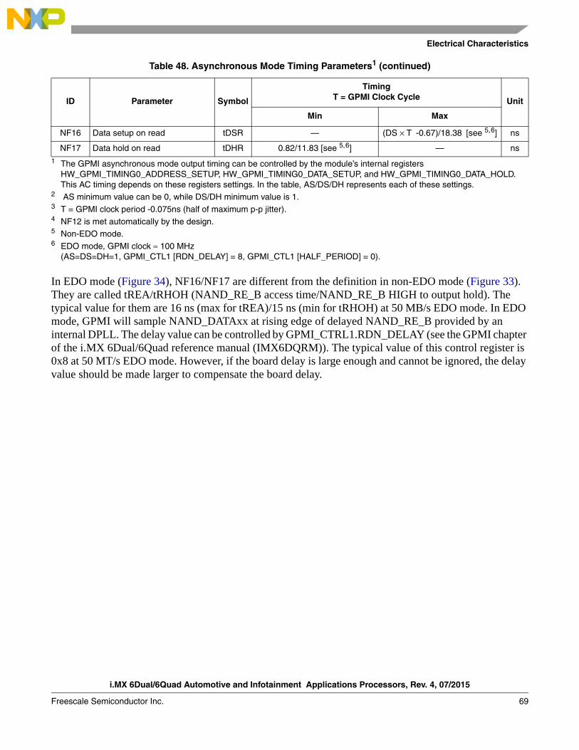
Electrical Characteristics
i.MX 6Dual/6Quad Automotive and Infotainment Applications Processors, Rev. 4, 07/2015
Freescale Semiconductor Inc. 69
In EDO mode (Figure 34), NF16/NF17 are different from the definition in non-EDO mode (Figure 33). They are called tREA/tRHOH (NAND_RE_B access time/NAND_RE_B HIGH to output hold). The typical value for them are 16 ns (max for tREA)/15 ns (min for tRHOH) at 50 MB/s EDO mode. In EDO mode, GPMI will sample NAND_DATAxx at rising edge of delayed NAND_RE_B provided by an internal DPLL. The delay value can be controlled by GPMI_CTRL1.RDN_DELAY (see the GPMI chapter of the i.MX 6Dual/6Quad reference manual (IMX6DQRM)). The typical value of this control register is 0x8 at 50 MT/s EDO mode. However, if the board delay is large enough and cannot be ignored, the delay value should be made larger to compensate the board delay.
NF16 Data setup on read tDSR — (DS × T -0.67)/18.38 [see 5,6] ns
NF17 Data hold on read tDHR 0.82/11.83 [see 5,6] — ns1 The GPMI asynchronous mode output timing can be controlled by the module’s internal registers
HW_GPMI_TIMING0_ADDRESS_SETUP, HW_GPMI_TIMING0_DATA_SETUP, and HW_GPMI_TIMING0_DATA_HOLD. This AC timing depends on these registers settings. In the table, AS/DS/DH represents each of these settings.
2 AS minimum value can be 0, while DS/DH minimum value is 1.3 T = GPMI clock period -0.075ns (half of maximum p-p jitter).4 NF12 is met automatically by the design.5 Non-EDO mode.6 EDO mode, GPMI clock ≈ 100 MHz
(AS=DS=DH=1, GPMI_CTL1 [RDN_DELAY] = 8, GPMI_CTL1 [HALF_PERIOD] = 0).
Table 48. Asynchronous Mode Timing Parameters1 (continued)
ID Parameter Symbol
TimingT = GPMI Clock Cycle Unit
Min Max
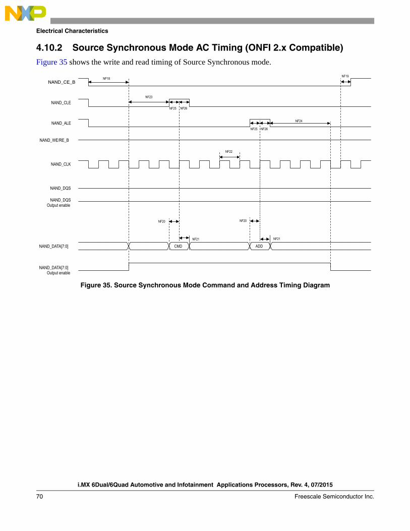
i.MX 6Dual/6Quad Automotive and Infotainment Applications Processors, Rev. 4, 07/2015
70 Freescale Semiconductor Inc.
Electrical Characteristics
4.10.2 Source Synchronous Mode AC Timing (ONFI 2.x Compatible)Figure 35 shows the write and read timing of Source Synchronous mode.
Figure 35. Source Synchronous Mode Command and Address Timing Diagram
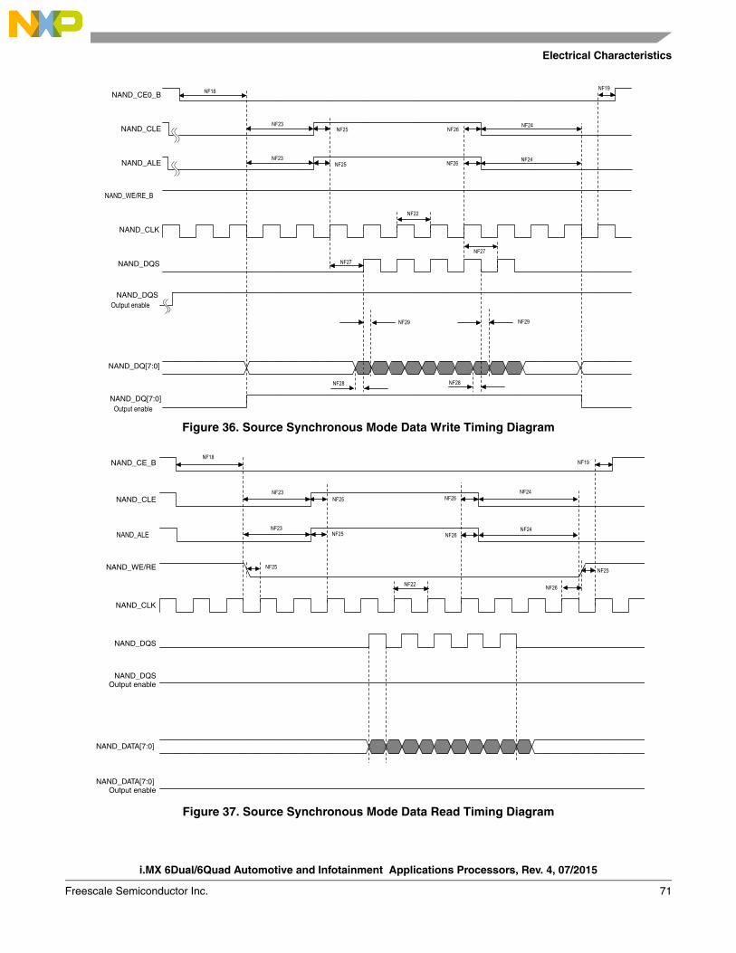
Electrical Characteristics
i.MX 6Dual/6Quad Automotive and Infotainment Applications Processors, Rev. 4, 07/2015
Freescale Semiconductor Inc. 71
Figure 36. Source Synchronous Mode Data Write Timing Diagram
Figure 37. Source Synchronous Mode Data Read Timing Diagram
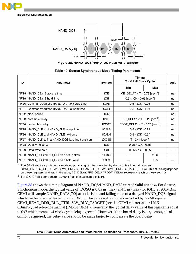
i.MX 6Dual/6Quad Automotive and Infotainment Applications Processors, Rev. 4, 07/2015
72 Freescale Semiconductor Inc.
Electrical Characteristics
Figure 38. NAND_DQS/NAND_DQ Read Valid Window
Figure 38 shows the timing diagram of NAND_DQS/NAND_DATAxx read valid window. For Source Synchronous mode, the typical value of tDQSQ is 0.85 ns (max) and 1 ns (max) for tQHS at 200MB/s. GPMI will sample NAND_DATA[7:0] at both rising and falling edge of a delayed NAND_DQS signal, which can be provided by an internal DPLL. The delay value can be controlled by GPMI register GPMI_READ_DDR_DLL_CTRL.SLV_DLY_TARGET (see the GPMI chapter of the i.MX 6Dual/6Quad reference manual (IMX6DQRM)). Generally, the typical delay value of this register is equal to 0x7 which means 1/4 clock cycle delay expected. However, if the board delay is large enough and cannot be ignored, the delay value should be made larger to compensate the board delay.
Table 49. Source Synchronous Mode Timing Parameters1
1 The GPMI source synchronous mode output timing can be controlled by the module’s internal registers GPMI_TIMING2_CE_DELAY, GPMI_TIMING_PREAMBLE_DELAY, GPMI_TIMING2_POST_DELAY. This AC timing depends on these registers settings. In the table, CE_DELAY/PRE_DELAY/POST_DELAY represents each of these settings.
ID Parameter Symbol
TimingT = GPMI Clock Cycle Unit
Min Max
NF18 NAND_CEx_B access time tCE CE_DELAY × T - 0.79 [see 2]
2 T = tCK (GPMI clock period) -0.075ns (half of maximum p-p jitter).
ns
NF19 NAND_CEx_B hold time tCH 0.5 × tCK - 0.63 [see 2] ns
NF20 Command/address NAND_DATAxx setup time tCAS 0.5 × tCK - 0.05 ns
NF21 Command/address NAND_DATAxx hold time tCAH 0.5 × tCK - 1.23 ns
NF22 clock period tCK — ns
NF23 preamble delay tPRE PRE_DELAY × T - 0.29 [see 2] ns
NF24 postamble delay tPOST POST_DELAY × T - 0.78 [see 2] ns
NF25 NAND_CLE and NAND_ALE setup time tCALS 0.5 × tCK - 0.86 ns
NF26 NAND_CLE and NAND_ALE hold time tCALH 0.5 × tCK - 0.37 ns
NF27 NAND_CLK to first NAND_DQS latching transition tDQSS T - 0.41 [see 2] ns
NF28 Data write setup tDS 0.25 × tCK - 0.35 —
NF29 Data write hold tDH 0.25 × tCK - 0.85 —
NF30 NAND_DQS/NAND_DQ read setup skew tDQSQ — 2.06 —
NF31 NAND_DQS/NAND_DQ read hold skew tQHS — 1.95 —
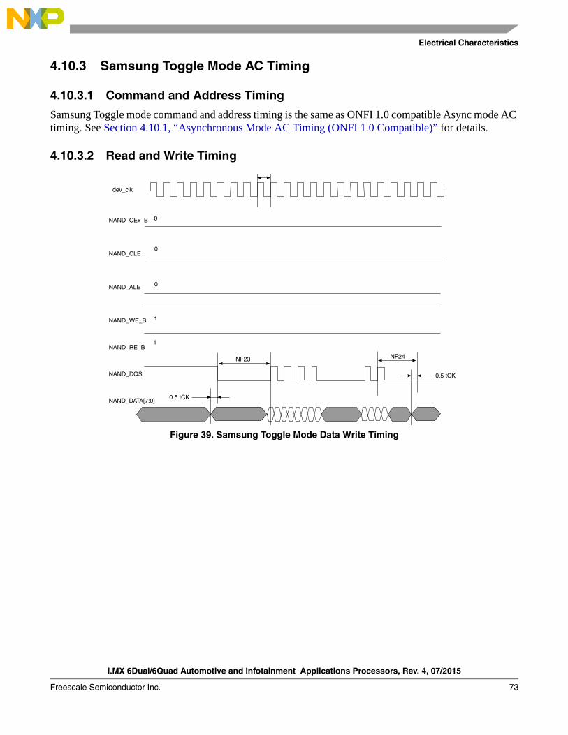
Electrical Characteristics
i.MX 6Dual/6Quad Automotive and Infotainment Applications Processors, Rev. 4, 07/2015
Freescale Semiconductor Inc. 73
4.10.3 Samsung Toggle Mode AC Timing
4.10.3.1 Command and Address Timing
Samsung Toggle mode command and address timing is the same as ONFI 1.0 compatible Async mode AC timing. See Section 4.10.1, “Asynchronous Mode AC Timing (ONFI 1.0 Compatible)” for details.
4.10.3.2 Read and Write Timing
Figure 39. Samsung Toggle Mode Data Write Timing
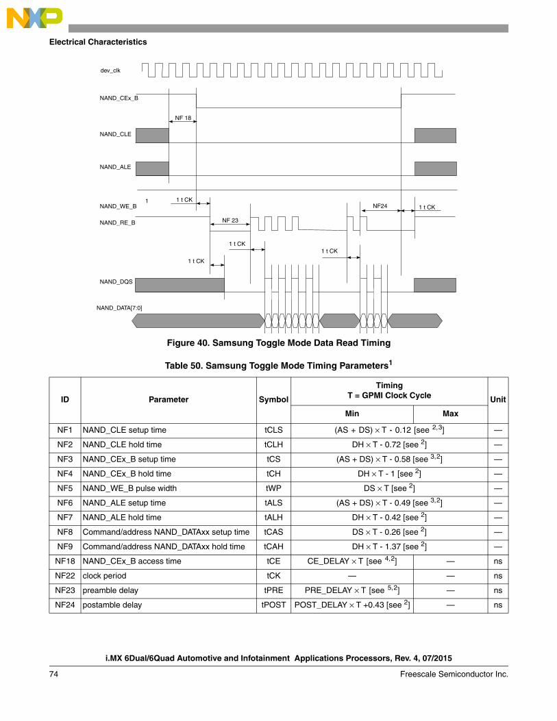
i.MX 6Dual/6Quad Automotive and Infotainment Applications Processors, Rev. 4, 07/2015
74 Freescale Semiconductor Inc.
Electrical Characteristics
Figure 40. Samsung Toggle Mode Data Read Timing
Table 50. Samsung Toggle Mode Timing Parameters1
ID Parameter Symbol
TimingT = GPMI Clock Cycle Unit
Min Max
NF1 NAND_CLE setup time tCLS (AS + DS) × T - 0.12 [see 2,3] —
NF2 NAND_CLE hold time tCLH DH × T - 0.72 [see 2] —
NF3 NAND_CEx_B setup time tCS (AS + DS) × T - 0.58 [see 3,2] —
NF4 NAND_CEx_B hold time tCH DH × T - 1 [see 2] —
NF5 NAND_WE_B pulse width tWP DS × T [see 2] —
NF6 NAND_ALE setup time tALS (AS + DS) × T - 0.49 [see 3,2] —
NF7 NAND_ALE hold time tALH DH × T - 0.42 [see 2] —
NF8 Command/address NAND_DATAxx setup time tCAS DS × T - 0.26 [see 2] —
NF9 Command/address NAND_DATAxx hold time tCAH DH × T - 1.37 [see 2] —
NF18 NAND_CEx_B access time tCE CE_DELAY × T [see 4,2] — ns
NF22 clock period tCK — — ns
NF23 preamble delay tPRE PRE_DELAY × T [see 5,2] — ns
NF24 postamble delay tPOST POST_DELAY × T +0.43 [see 2] — ns
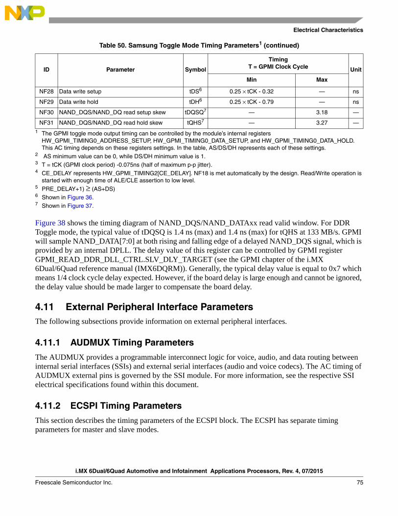
Electrical Characteristics
i.MX 6Dual/6Quad Automotive and Infotainment Applications Processors, Rev. 4, 07/2015
Freescale Semiconductor Inc. 75
Figure 38 shows the timing diagram of NAND_DQS/NAND_DATAxx read valid window. For DDR Toggle mode, the typical value of tDQSQ is 1.4 ns (max) and 1.4 ns (max) for tQHS at 133 MB/s. GPMI will sample NAND_DATA[7:0] at both rising and falling edge of a delayed NAND_DQS signal, which is provided by an internal DPLL. The delay value of this register can be controlled by GPMI register GPMI_READ_DDR_DLL_CTRL.SLV_DLY_TARGET (see the GPMI chapter of the i.MX 6Dual/6Quad reference manual (IMX6DQRM)). Generally, the typical delay value is equal to 0x7 which means 1/4 clock cycle delay expected. However, if the board delay is large enough and cannot be ignored, the delay value should be made larger to compensate the board delay.
4.11 External Peripheral Interface ParametersThe following subsections provide information on external peripheral interfaces.
4.11.1 AUDMUX Timing Parameters
The AUDMUX provides a programmable interconnect logic for voice, audio, and data routing between internal serial interfaces (SSIs) and external serial interfaces (audio and voice codecs). The AC timing of AUDMUX external pins is governed by the SSI module. For more information, see the respective SSI electrical specifications found within this document.
4.11.2 ECSPI Timing Parameters
This section describes the timing parameters of the ECSPI block. The ECSPI has separate timing parameters for master and slave modes.
NF28 Data write setup tDS6 0.25 × tCK - 0.32 — ns
NF29 Data write hold tDH6 0.25 × tCK - 0.79 — ns
NF30 NAND_DQS/NAND_DQ read setup skew tDQSQ7 — 3.18 —
NF31 NAND_DQS/NAND_DQ read hold skew tQHS7 — 3.27 —1 The GPMI toggle mode output timing can be controlled by the module’s internal registers
HW_GPMI_TIMING0_ADDRESS_SETUP, HW_GPMI_TIMING0_DATA_SETUP, and HW_GPMI_TIMING0_DATA_HOLD. This AC timing depends on these registers settings. In the table, AS/DS/DH represents each of these settings.
2 AS minimum value can be 0, while DS/DH minimum value is 1.3 T = tCK (GPMI clock period) -0.075ns (half of maximum p-p jitter).4 CE_DELAY represents HW_GPMI_TIMING2[CE_DELAY]. NF18 is met automatically by the design. Read/Write operation is
started with enough time of ALE/CLE assertion to low level.5 PRE_DELAY+1) ≥ (AS+DS)6 Shown in Figure 36.7 Shown in Figure 37.
Table 50. Samsung Toggle Mode Timing Parameters1 (continued)
ID Parameter Symbol
TimingT = GPMI Clock Cycle Unit
Min Max
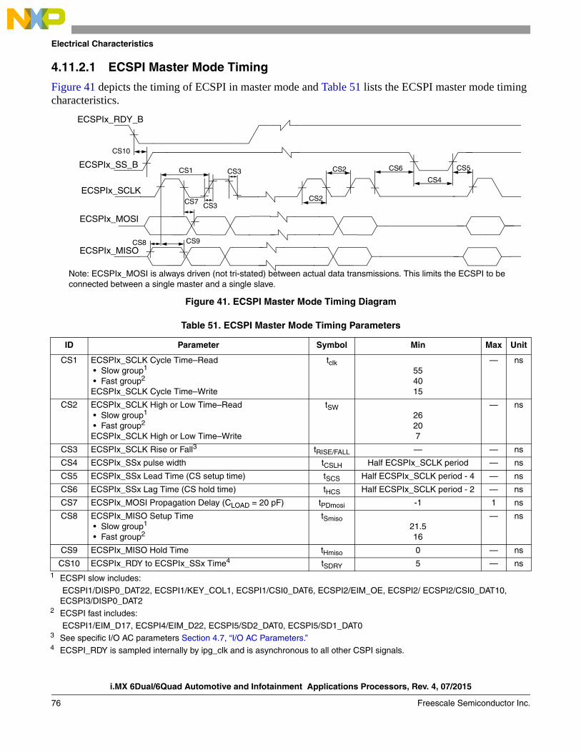
i.MX 6Dual/6Quad Automotive and Infotainment Applications Processors, Rev. 4, 07/2015
76 Freescale Semiconductor Inc.
Electrical Characteristics
4.11.2.1 ECSPI Master Mode Timing
Figure 41 depicts the timing of ECSPI in master mode and Table 51 lists the ECSPI master mode timing characteristics.
Figure 41. ECSPI Master Mode Timing Diagram
Table 51. ECSPI Master Mode Timing Parameters
ID Parameter Symbol Min Max Unit
CS1 ECSPIx_SCLK Cycle Time–Read • Slow group1
• Fast group2
ECSPIx_SCLK Cycle Time–Write
1 ECSPI slow includes:
ECSPI1/DISP0_DAT22, ECSPI1/KEY_COL1, ECSPI1/CSI0_DAT6, ECSPI2/EIM_OE, ECSPI2/ ECSPI2/CSI0_DAT10, ECSPI3/DISP0_DAT2
2 ECSPI fast includes:
ECSPI1/EIM_D17, ECSPI4/EIM_D22, ECSPI5/SD2_DAT0, ECSPI5/SD1_DAT0
tclk554015
— ns
CS2 ECSPIx_SCLK High or Low Time–Read • Slow group1
• Fast group2
ECSPIx_SCLK High or Low Time–Write
tSW26207
— ns
CS3 ECSPIx_SCLK Rise or Fall3
3 See specific I/O AC parameters Section 4.7, “I/O AC Parameters.”
tRISE/FALL — — ns
CS4 ECSPIx_SSx pulse width tCSLH Half ECSPIx_SCLK period — ns
CS5 ECSPIx_SSx Lead Time (CS setup time) tSCS Half ECSPIx_SCLK period - 4 — ns
CS6 ECSPIx_SSx Lag Time (CS hold time) tHCS Half ECSPIx_SCLK period - 2 — ns
CS7 ECSPIx_MOSI Propagation Delay (CLOAD = 20 pF) tPDmosi -1 1 ns
CS8 ECSPIx_MISO Setup Time • Slow group1
• Fast group2
tSmiso21.516
— ns
CS9 ECSPIx_MISO Hold Time tHmiso 0 — ns
CS10 ECSPIx_RDY to ECSPIx_SSx Time4
4 ECSPI_RDY is sampled internally by ipg_clk and is asynchronous to all other CSPI signals.
tSDRY 5 — ns
CS1
CS7
CS2
CS2
CS4
CS6 CS5
CS8 CS9
ECSPIx_SCLK
ECSPIx_SS_B
ECSPIx_MOSI
ECSPIx_MISO
ECSPIx_RDY_B
CS10
CS3
CS3
Note: ECSPIx_MOSI is always driven (not tri-stated) between actual data transmissions. This limits the ECSPI to be connected between a single master and a single slave.
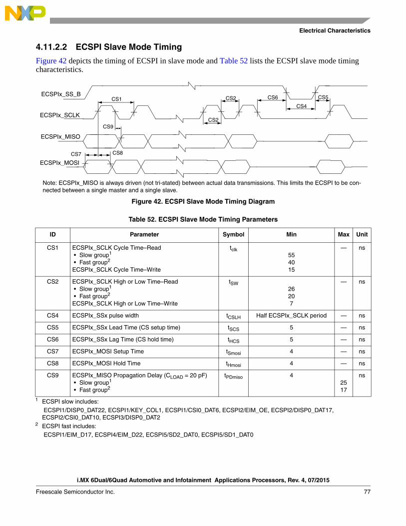
Electrical Characteristics
i.MX 6Dual/6Quad Automotive and Infotainment Applications Processors, Rev. 4, 07/2015
Freescale Semiconductor Inc. 77
4.11.2.2 ECSPI Slave Mode Timing
Figure 42 depicts the timing of ECSPI in slave mode and Table 52 lists the ECSPI slave mode timing characteristics.
Figure 42. ECSPI Slave Mode Timing Diagram
Table 52. ECSPI Slave Mode Timing Parameters
ID Parameter Symbol Min Max Unit
CS1 ECSPIx_SCLK Cycle Time–Read • Slow group1
• Fast group2
ECSPIx_SCLK Cycle Time–Write
1 ECSPI slow includes:
ECSPI1/DISP0_DAT22, ECSPI1/KEY_COL1, ECSPI1/CSI0_DAT6, ECSPI2/EIM_OE, ECSPI2/DISP0_DAT17, ECSPI2/CSI0_DAT10, ECSPI3/DISP0_DAT2
2 ECSPI fast includes: ECSPI1/EIM_D17, ECSPI4/EIM_D22, ECSPI5/SD2_DAT0, ECSPI5/SD1_DAT0
tclk554015
— ns
CS2 ECSPIx_SCLK High or Low Time–Read • Slow group1
• Fast group2
ECSPIx_SCLK High or Low Time–Write
tSW26207
— ns
CS4 ECSPIx_SSx pulse width tCSLH Half ECSPIx_SCLK period — ns
CS5 ECSPIx_SSx Lead Time (CS setup time) tSCS 5 — ns
CS6 ECSPIx_SSx Lag Time (CS hold time) tHCS 5 — ns
CS7 ECSPIx_MOSI Setup Time tSmosi 4 — ns
CS8 ECSPIx_MOSI Hold Time tHmosi 4 — ns
CS9 ECSPIx_MISO Propagation Delay (CLOAD = 20 pF) • Slow group1
• Fast group2
tPDmiso 42517
ns
CS1
CS7 CS8
CS2
CS2
CS4
CS6 CS5
CS9
ECSPIx_SCLK
ECSPIx_SS_B
ECSPIx_MISO
ECSPIx_MOSI
Note: ECSPIx_MISO is always driven (not tri-stated) between actual data transmissions. This limits the ECSPI to be con-nected between a single master and a single slave.
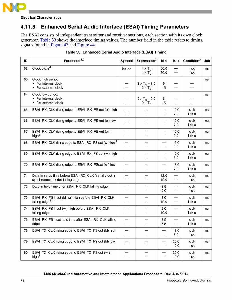
i.MX 6Dual/6Quad Automotive and Infotainment Applications Processors, Rev. 4, 07/2015
78 Freescale Semiconductor Inc.
Electrical Characteristics
4.11.3 Enhanced Serial Audio Interface (ESAI) Timing ParametersThe ESAI consists of independent transmitter and receiver sections, each section with its own clock generator. Table 53 shows the interface timing values. The number field in the table refers to timing signals found in Figure 43 and Figure 44.
Table 53. Enhanced Serial Audio Interface (ESAI) Timing
ID Parameter1,2 Symbol Expression2 Min Max Condition3 Unit
62 Clock cycle4 tSSICC 4 × Tc4 × Tc
30.030.0
——
i cki ck
ns
63 Clock high period: • For internal clock • For external clock
——
2 × Tc − 9.02 × Tc
615
——
——
ns
64 Clock low period: • For internal clock • For external clock
——
2 × Tc − 9.02 × Tc
615
——
——
ns
65 ESAI_RX_CLK rising edge to ESAI_RX_FS out (bl) high ——
——
——
19.07.0
x cki ck a
ns
66 ESAI_RX_CLK rising edge to ESAI_RX_FS out (bl) low ——
——
——
19.07.0
x cki ck a
ns
67 ESAI_RX_CLK rising edge to ESAI_RX_FS out (wr) high5
——
——
——
19.09.0
x cki ck a
ns
68 ESAI_RX_CLK rising edge to ESAI_RX_FS out (wr) low5 ——
——
——
19.09.0
x cki ck a
ns
69 ESAI_RX_CLK rising edge to ESAI_RX_FS out (wl) high ——
——
——
19.06.0
x cki ck a
ns
70 ESAI_RX_CLK rising edge to ESAI_RX_FSout (wl) low ——
——
——
17.07.0
x cki ck a
ns
71 Data in setup time before ESAI_RX_CLK (serial clock in synchronous mode) falling edge
——
——
12.019.0
——
x cki ck
ns
72 Data in hold time after ESAI_RX_CLK falling edge ——
——
3.59.0
——
x cki ck
ns
73 ESAI_RX_FS input (bl, wr) high before ESAI_RX_CLK falling edge5
——
——
2.019.0
——
x cki ck a
ns
74 ESAI_RX_FS input (wl) high before ESAI_RX_CLK falling edge
——
——
2.019.0
——
x cki ck a
ns
75 ESAI_RX_FS input hold time after ESAI_RX_CLK falling edge
——
——
2.58.5
——
x cki ck a
ns
78 ESAI_TX_CLK rising edge to ESAI_TX_FS out (bl) high ——
——
——
19.08.0
x cki ck
ns
79 ESAI_TX_CLK rising edge to ESAI_TX_FS out (bl) low ——
——
——
20.010.0
x cki ck
ns
80 ESAI_TX_CLK rising edge to ESAI_TX_FS out (wr) high5
——
——
——
20.010.0
x cki ck
ns
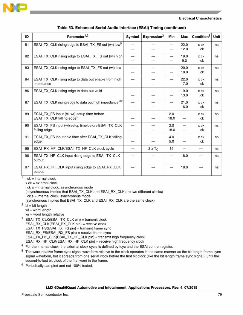
Electrical Characteristics
i.MX 6Dual/6Quad Automotive and Infotainment Applications Processors, Rev. 4, 07/2015
Freescale Semiconductor Inc. 79
81 ESAI_TX_CLK rising edge to ESAI_TX_FS out (wr) low5 ——
——
——
22.012.0
x cki ck
ns
82 ESAI_TX_CLK rising edge to ESAI_TX_FS out (wl) high ——
——
——
19.09.0
x cki ck
ns
83 ESAI_TX_CLK rising edge to ESAI_TX_FS out (wl) low ——
——
——
20.010.0
x cki ck
ns
84 ESAI_TX_CLK rising edge to data out enable from high impedance
——
——
——
22.017.0
x cki ck
ns
86 ESAI_TX_CLK rising edge to data out valid ——
——
——
19.013.0
x cki ck
ns
87 ESAI_TX_CLK rising edge to data out high impedance 67 ——
——
——
21.016.0
x cki ck
ns
89 ESAI_TX_FS input (bl, wr) setup time before ESAI_TX_CLK falling edge5
——
——
2.018.0
——
x cki ck
ns
90 ESAI_TX_FS input (wl) setup time before ESAI_TX_CLK falling edge
——
——
2.018.0
——
x cki ck
ns
91 ESAI_TX_FS input hold time after ESAI_TX_CLK falling edge
——
——
4.05.0
——
x cki ck
ns
95 ESAI_RX_HF_CLK/ESAI_TX_HF_CLK clock cycle — 2 x TC 15 — — ns
96 ESAI_TX_HF_CLK input rising edge to ESAI_TX_CLK output
— — — 18.0 — ns
97 ESAI_RX_HF_CLK input rising edge to ESAI_RX_CLK output
— — — 18.0 — ns
1 i ck = internal clockx ck = external clocki ck a = internal clock, asynchronous mode (asynchronous implies that ESAI_TX_CLK and ESAI_RX_CLK are two different clocks)i ck s = internal clock, synchronous mode (synchronous implies that ESAI_TX_CLK and ESAI_RX_CLK are the same clock)
2 bl = bit lengthwl = word lengthwr = word length relative
3 ESAI_TX_CLK(ESAI_TX_CLK pin) = transmit clockESAI_RX_CLK(ESAI_RX_CLK pin) = receive clockESAI_TX_FS(ESAI_TX_FS pin) = transmit frame syncESAI_RX_FS(ESAI_RX_FS pin) = receive frame syncESAI_TX_HF_CLK(ESAI_TX_HF_CLK pin) = transmit high frequency clockESAI_RX_HF_CLK(ESAI_RX_HF_CLK pin) = receive high frequency clock
4 For the internal clock, the external clock cycle is defined by Icyc and the ESAI control register.5 The word-relative frame sync signal waveform relative to the clock operates in the same manner as the bit-length frame sync
signal waveform, but it spreads from one serial clock before the first bit clock (like the bit length frame sync signal), until the second-to-last bit clock of the first word in the frame.
6 Periodically sampled and not 100% tested.
Table 53. Enhanced Serial Audio Interface (ESAI) Timing (continued)
ID Parameter1,2 Symbol Expression2 Min Max Condition3 Unit
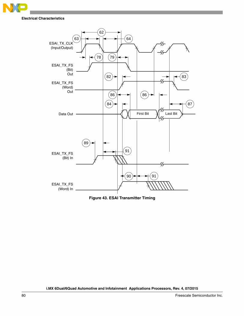
i.MX 6Dual/6Quad Automotive and Infotainment Applications Processors, Rev. 4, 07/2015
80 Freescale Semiconductor Inc.
Electrical Characteristics
Figure 43. ESAI Transmitter Timing
ESAI_TX_CLK(Input/Output)
ESAI_TX_FS(Bit)Out
ESAI_TX_FS(Word)
Out
Data Out
ESAI_TX_FS(Bit) In
ESAI_TX_FS(Word) In
62
64
78 79
82 83
87
8686
84
91
89
90 91
63
Last BitFirst Bit
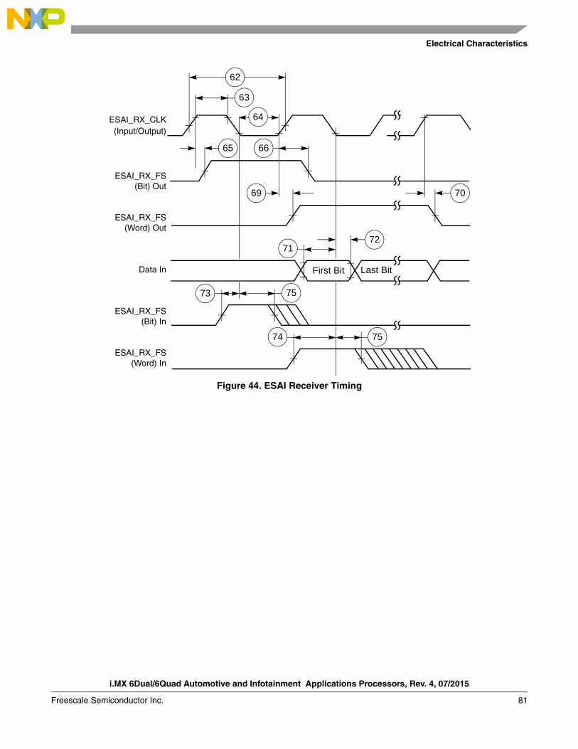
Electrical Characteristics
i.MX 6Dual/6Quad Automotive and Infotainment Applications Processors, Rev. 4, 07/2015
Freescale Semiconductor Inc. 81
Figure 44. ESAI Receiver Timing
ESAI_RX_CLK(Input/Output)
ESAI_RX_FS(Bit) Out
ESAI_RX_FS(Word) Out
Data In
ESAI_RX_FS(Bit) In
ESAI_RX_FS(Word) In
62
64
65
69 70
7271
7573
74 75
63
66
First Bit Last Bit
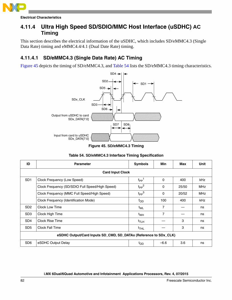
i.MX 6Dual/6Quad Automotive and Infotainment Applications Processors, Rev. 4, 07/2015
82 Freescale Semiconductor Inc.
Electrical Characteristics
4.11.4 Ultra High Speed SD/SDIO/MMC Host Interface (uSDHC) AC Timing
This section describes the electrical information of the uSDHC, which includes SD/eMMC4.3 (Single Data Rate) timing and eMMC4.4/4.1 (Dual Date Rate) timing.
4.11.4.1 SD/eMMC4.3 (Single Data Rate) AC Timing
Figure 45 depicts the timing of SD/eMMC4.3, and Table 54 lists the SD/eMMC4.3 timing characteristics.
Figure 45. SD/eMMC4.3 Timing
Table 54. SD/eMMC4.3 Interface Timing Specification
ID Parameter Symbols Min Max Unit
Card Input Clock
SD1 Clock Frequency (Low Speed) fPP1 0 400 kHz
Clock Frequency (SD/SDIO Full Speed/High Speed) fPP2 0 25/50 MHz
Clock Frequency (MMC Full Speed/High Speed) fPP3 0 20/52 MHz
Clock Frequency (Identification Mode) fOD 100 400 kHz
SD2 Clock Low Time tWL 7 — ns
SD3 Clock High Time tWH 7 — ns
SD4 Clock Rise Time tTLH — 3 ns
SD5 Clock Fall Time tTHL — 3 ns
eSDHC Output/Card Inputs SD_CMD, SD_DATAx (Reference to SDx_CLK)
SD6 eSDHC Output Delay tOD –6.6 3.6 ns
SD1
SD3
SD5
SD4
SD7
SDx_CLK
SD2
SD8
SD6
Output from uSDHC to card
Input from card to uSDHCSDx_DATA[7:0]
SDx_DATA[7:0]
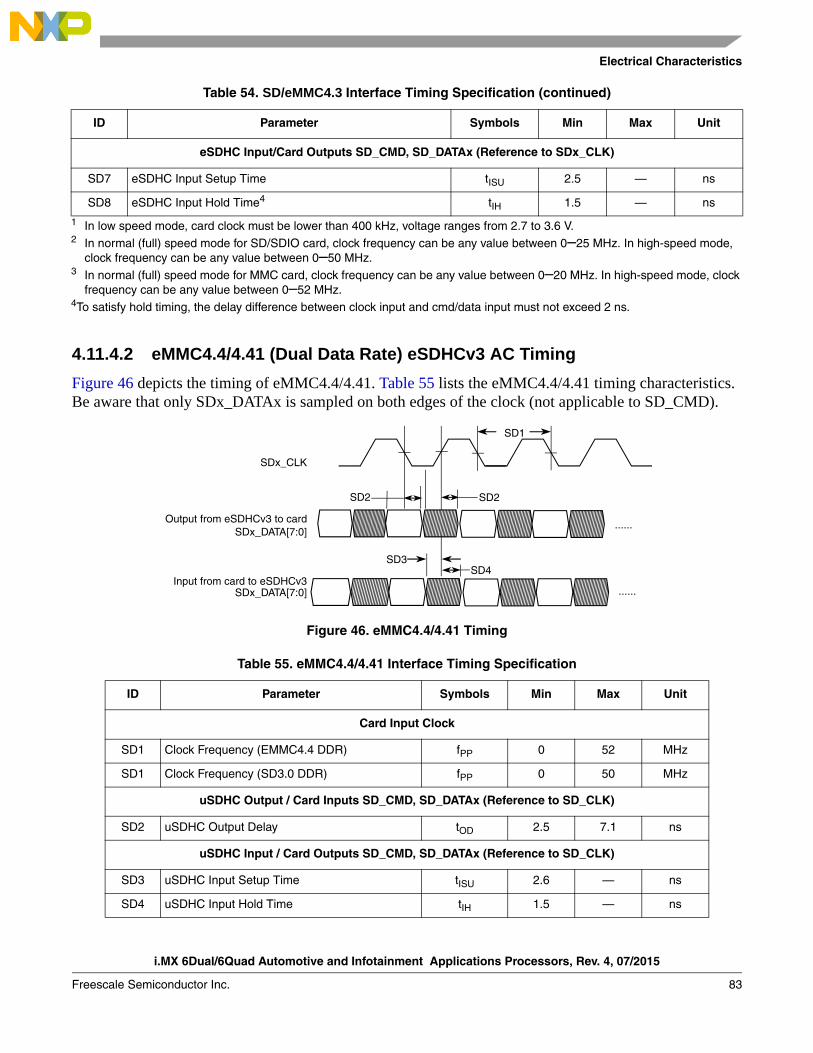
Electrical Characteristics
i.MX 6Dual/6Quad Automotive and Infotainment Applications Processors, Rev. 4, 07/2015
Freescale Semiconductor Inc. 83
4.11.4.2 eMMC4.4/4.41 (Dual Data Rate) eSDHCv3 AC Timing
Figure 46 depicts the timing of eMMC4.4/4.41. Table 55 lists the eMMC4.4/4.41 timing characteristics. Be aware that only SDx_DATAx is sampled on both edges of the clock (not applicable to SD_CMD).
Figure 46. eMMC4.4/4.41 Timing
eSDHC Input/Card Outputs SD_CMD, SD_DATAx (Reference to SDx_CLK)
SD7 eSDHC Input Setup Time tISU 2.5 — ns
SD8 eSDHC Input Hold Time4 tIH 1.5 — ns
1 In low speed mode, card clock must be lower than 400 kHz, voltage ranges from 2.7 to 3.6 V.2 In normal (full) speed mode for SD/SDIO card, clock frequency can be any value between 0–25 MHz. In high-speed mode,
clock frequency can be any value between 0–50 MHz.3 In normal (full) speed mode for MMC card, clock frequency can be any value between 0–20 MHz. In high-speed mode, clock
frequency can be any value between 0–52 MHz.4To satisfy hold timing, the delay difference between clock input and cmd/data input must not exceed 2 ns.
Table 55. eMMC4.4/4.41 Interface Timing Specification
ID Parameter Symbols Min Max Unit
Card Input Clock
SD1 Clock Frequency (EMMC4.4 DDR) fPP 0 52 MHz
SD1 Clock Frequency (SD3.0 DDR) fPP 0 50 MHz
uSDHC Output / Card Inputs SD_CMD, SD_DATAx (Reference to SD_CLK)
SD2 uSDHC Output Delay tOD 2.5 7.1 ns
uSDHC Input / Card Outputs SD_CMD, SD_DATAx (Reference to SD_CLK)
SD3 uSDHC Input Setup Time tISU 2.6 — ns
SD4 uSDHC Input Hold Time tIH 1.5 — ns
Table 54. SD/eMMC4.3 Interface Timing Specification (continued)
ID Parameter Symbols Min Max Unit
SD1
SD3
Output from eSDHCv3 to card
Input from card to eSDHCv3SDx_DATA[7:0]
SDx_CLK
SD4
SD2
......
......
SDx_DATA[7:0]
SD2
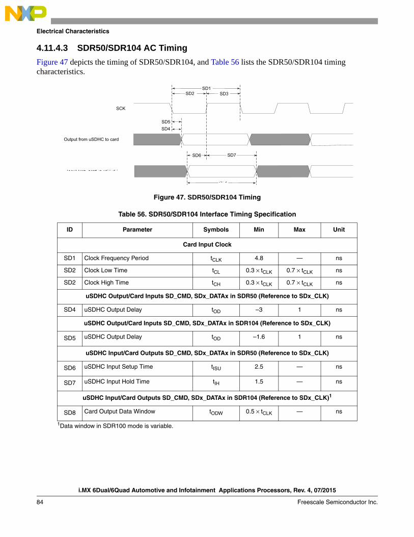
i.MX 6Dual/6Quad Automotive and Infotainment Applications Processors, Rev. 4, 07/2015
84 Freescale Semiconductor Inc.
Electrical Characteristics
4.11.4.3 SDR50/SDR104 AC Timing
Figure 47 depicts the timing of SDR50/SDR104, and Table 56 lists the SDR50/SDR104 timing characteristics.
Figure 47. SDR50/SDR104 Timing
Table 56. SDR50/SDR104 Interface Timing Specification
ID Parameter Symbols Min Max Unit
Card Input Clock
SD1 Clock Frequency Period tCLK 4.8 — ns
SD2 Clock Low Time tCL 0.3 × tCLK 0.7 × tCLK ns
SD2 Clock High Time tCH 0.3 × tCLK 0.7 × tCLK ns
uSDHC Output/Card Inputs SD_CMD, SDx_DATAx in SDR50 (Reference to SDx_CLK)
SD4 uSDHC Output Delay tOD –3 1 ns
uSDHC Output/Card Inputs SD_CMD, SDx_DATAx in SDR104 (Reference to SDx_CLK)
SD5 uSDHC Output Delay tOD –1.6 1 ns
uSDHC Input/Card Outputs SD_CMD, SDx_DATAx in SDR50 (Reference to SDx_CLK)
SD6 uSDHC Input Setup Time tISU 2.5 — ns
SD7 uSDHC Input Hold Time tIH 1.5 — ns
uSDHC Input/Card Outputs SD_CMD, SDx_DATAx in SDR104 (Reference to SDx_CLK)1
1Data window in SDR100 mode is variable.
SD8 Card Output Data Window tODW 0.5 × tCLK — ns
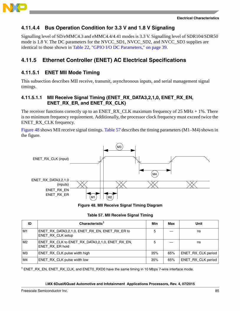
Electrical Characteristics
i.MX 6Dual/6Quad Automotive and Infotainment Applications Processors, Rev. 4, 07/2015
Freescale Semiconductor Inc. 85
4.11.4.4 Bus Operation Condition for 3.3 V and 1.8 V Signaling
Signalling level of SD/eMMC4.3 and eMMC4.4/4.41 modes is 3.3 V. Signalling level of SDR104/SDR50 mode is 1.8 V. The DC parameters for the NVCC_SD1, NVCC_SD2, and NVCC_SD3 supplies are identical to those shown in Table 22, "GPIO I/O DC Parameters," on page 39.
4.11.5 Ethernet Controller (ENET) AC Electrical Specifications
4.11.5.1 ENET MII Mode Timing
This subsection describes MII receive, transmit, asynchronous inputs, and serial management signal timings.
4.11.5.1.1 MII Receive Signal Timing (ENET_RX_DATA3,2,1,0, ENET_RX_EN, ENET_RX_ER, and ENET_RX_CLK)
The receiver functions correctly up to an ENET_RX_CLK maximum frequency of 25 MHz + 1%. There is no minimum frequency requirement. Additionally, the processor clock frequency must exceed twice the ENET_RX_CLK frequency.
Figure 48 shows MII receive signal timings. Table 57 describes the timing parameters (M1–M4) shown in the figure.
Figure 48. MII Receive Signal Timing Diagram
1 ENET_RX_EN, ENET_RX_CLK, and ENET0_RXD0 have the same timing in 10 Mbps 7-wire interface mode.
Table 57. MII Receive Signal Timing
ID Characteristic1 Min Max Unit
M1 ENET_RX_DATA3,2,1,0, ENET_RX_EN, ENET_RX_ER to ENET_RX_CLK setup
5 — ns
M2 ENET_RX_CLK to ENET_RX_DATA3,2,1,0, ENET_RX_EN, ENET_RX_ER hold
5 — ns
M3 ENET_RX_CLK pulse width high 35% 65% ENET_RX_CLK period
M4 ENET_RX_CLK pulse width low 35% 65% ENET_RX_CLK period
ENET_RX_CLK (input)
ENET_RX_DATA3,2,1,0
M3
M4
M1 M2ENET_RX_ERENET_RX_EN
(inputs)
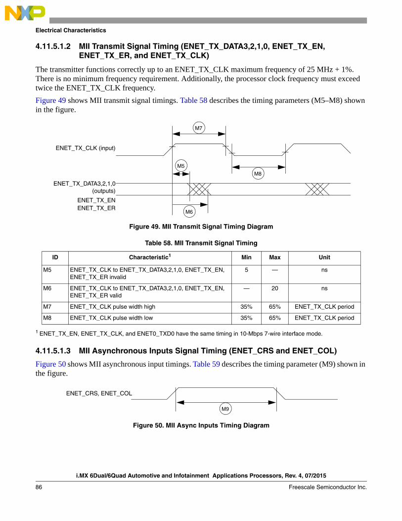
i.MX 6Dual/6Quad Automotive and Infotainment Applications Processors, Rev. 4, 07/2015
86 Freescale Semiconductor Inc.
Electrical Characteristics
4.11.5.1.2 MII Transmit Signal Timing (ENET_TX_DATA3,2,1,0, ENET_TX_EN, ENET_TX_ER, and ENET_TX_CLK)
The transmitter functions correctly up to an ENET_TX_CLK maximum frequency of 25 MHz + 1%. There is no minimum frequency requirement. Additionally, the processor clock frequency must exceed twice the ENET_TX_CLK frequency.
Figure 49 shows MII transmit signal timings. Table 58 describes the timing parameters (M5–M8) shown in the figure.
Figure 49. MII Transmit Signal Timing Diagram
1 ENET_TX_EN, ENET_TX_CLK, and ENET0_TXD0 have the same timing in 10-Mbps 7-wire interface mode.
4.11.5.1.3 MII Asynchronous Inputs Signal Timing (ENET_CRS and ENET_COL)
Figure 50 shows MII asynchronous input timings. Table 59 describes the timing parameter (M9) shown in the figure.
Figure 50. MII Async Inputs Timing Diagram
Table 58. MII Transmit Signal Timing
ID Characteristic1 Min Max Unit
M5 ENET_TX_CLK to ENET_TX_DATA3,2,1,0, ENET_TX_EN, ENET_TX_ER invalid
5 — ns
M6 ENET_TX_CLK to ENET_TX_DATA3,2,1,0, ENET_TX_EN, ENET_TX_ER valid
— 20 ns
M7 ENET_TX_CLK pulse width high 35% 65% ENET_TX_CLK period
M8 ENET_TX_CLK pulse width low 35% 65% ENET_TX_CLK period
ENET_TX_CLK (input)
ENET_TX_DATA3,2,1,0
M7
M8
M5
M6ENET_TX_ERENET_TX_EN
(outputs)
ENET_CRS, ENET_COL
M9
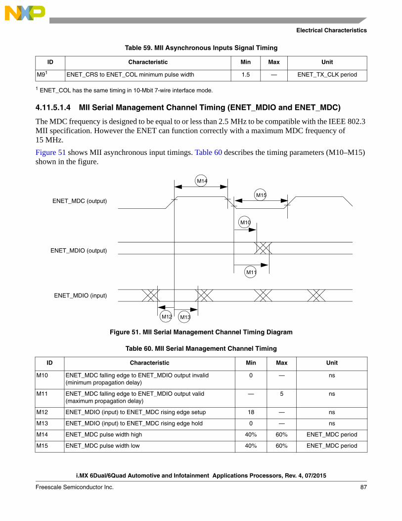
Electrical Characteristics
i.MX 6Dual/6Quad Automotive and Infotainment Applications Processors, Rev. 4, 07/2015
Freescale Semiconductor Inc. 87
1 ENET_COL has the same timing in 10-Mbit 7-wire interface mode.
4.11.5.1.4 MII Serial Management Channel Timing (ENET_MDIO and ENET_MDC)
The MDC frequency is designed to be equal to or less than 2.5 MHz to be compatible with the IEEE 802.3 MII specification. However the ENET can function correctly with a maximum MDC frequency of 15 MHz.
Figure 51 shows MII asynchronous input timings. Table 60 describes the timing parameters (M10–M15) shown in the figure.
Figure 51. MII Serial Management Channel Timing Diagram
Table 59. MII Asynchronous Inputs Signal Timing
ID Characteristic Min Max Unit
M91 ENET_CRS to ENET_COL minimum pulse width 1.5 — ENET_TX_CLK period
Table 60. MII Serial Management Channel Timing
ID Characteristic Min Max Unit
M10 ENET_MDC falling edge to ENET_MDIO output invalid (minimum propagation delay)
0 — ns
M11 ENET_MDC falling edge to ENET_MDIO output valid(maximum propagation delay)
— 5 ns
M12 ENET_MDIO (input) to ENET_MDC rising edge setup 18 — ns
M13 ENET_MDIO (input) to ENET_MDC rising edge hold 0 — ns
M14 ENET_MDC pulse width high 40% 60% ENET_MDC period
M15 ENET_MDC pulse width low 40% 60% ENET_MDC period
ENET_MDC (output)
ENET_MDIO (output)
M14
M15
M10
M11
M12 M13
ENET_MDIO (input)
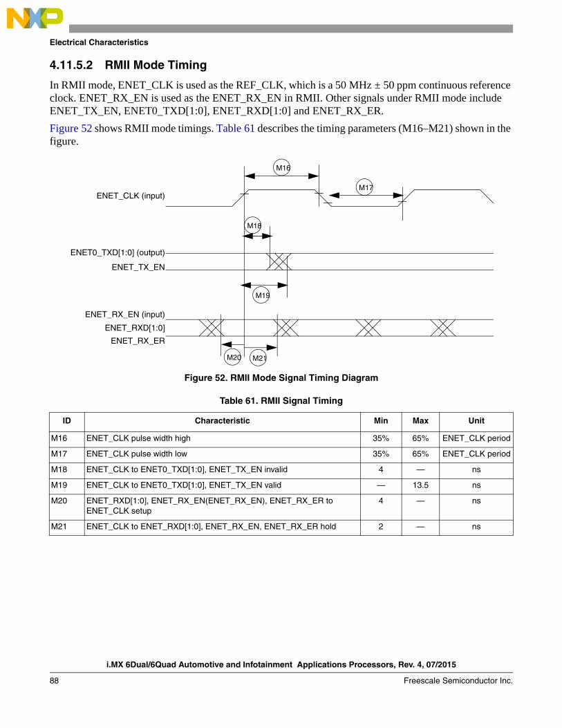
i.MX 6Dual/6Quad Automotive and Infotainment Applications Processors, Rev. 4, 07/2015
88 Freescale Semiconductor Inc.
Electrical Characteristics
4.11.5.2 RMII Mode Timing
In RMII mode, ENET_CLK is used as the REF_CLK, which is a 50 MHz ± 50 ppm continuous reference clock. ENET_RX_EN is used as the ENET_RX_EN in RMII. Other signals under RMII mode include ENET_TX_EN, ENET0_TXD[1:0], ENET_RXD[1:0] and ENET_RX_ER.
Figure 52 shows RMII mode timings. Table 61 describes the timing parameters (M16–M21) shown in the figure.
Figure 52. RMII Mode Signal Timing Diagram
Table 61. RMII Signal Timing
ID Characteristic Min Max Unit
M16 ENET_CLK pulse width high 35% 65% ENET_CLK period
M17 ENET_CLK pulse width low 35% 65% ENET_CLK period
M18 ENET_CLK to ENET0_TXD[1:0], ENET_TX_EN invalid 4 — ns
M19 ENET_CLK to ENET0_TXD[1:0], ENET_TX_EN valid — 13.5 ns
M20 ENET_RXD[1:0], ENET_RX_EN(ENET_RX_EN), ENET_RX_ER to ENET_CLK setup
4 — ns
M21 ENET_CLK to ENET_RXD[1:0], ENET_RX_EN, ENET_RX_ER hold 2 — ns
ENET_CLK (input)
ENET_TX_EN
M16
M17
M18
M19
M20 M21
ENET_RXD[1:0]
ENET0_TXD[1:0] (output)
ENET_RX_ER
ENET_RX_EN (input)
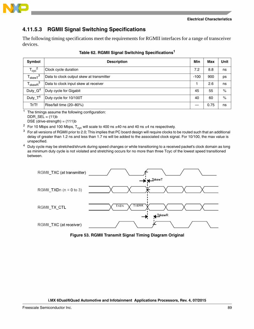
Electrical Characteristics
i.MX 6Dual/6Quad Automotive and Infotainment Applications Processors, Rev. 4, 07/2015
Freescale Semiconductor Inc. 89
4.11.5.3 RGMII Signal Switching Specifications
The following timing specifications meet the requirements for RGMII interfaces for a range of transceiver devices.
Figure 53. RGMII Transmit Signal Timing Diagram Original
Table 62. RGMII Signal Switching Specifications1
1 The timings assume the following configuration:DDR_SEL = (11)bDSE (drive-strength) = (111)b
Symbol Description Min Max Unit
Tcyc2
2 For 10 Mbps and 100 Mbps, Tcyc will scale to 400 ns ±40 ns and 40 ns ±4 ns respectively.
Clock cycle duration 7.2 8.8 ns
TskewT3
3 For all versions of RGMII prior to 2.0; This implies that PC board design will require clocks to be routed such that an additional delay of greater than 1.2 ns and less than 1.7 ns will be added to the associated clock signal. For 10/100, the max value is unspecified.
Data to clock output skew at transmitter -100 900 ps
TskewR3 Data to clock input skew at receiver 1 2.6 ns
Duty_G4
4 Duty cycle may be stretched/shrunk during speed changes or while transitioning to a received packet's clock domain as long as minimum duty cycle is not violated and stretching occurs for no more than three Tcyc of the lowest speed transitioned between.
Duty cycle for Gigabit 45 55 %
Duty_T4 Duty cycle for 10/100T 40 60 %
Tr/Tf Rise/fall time (20–80%) — 0.75 ns
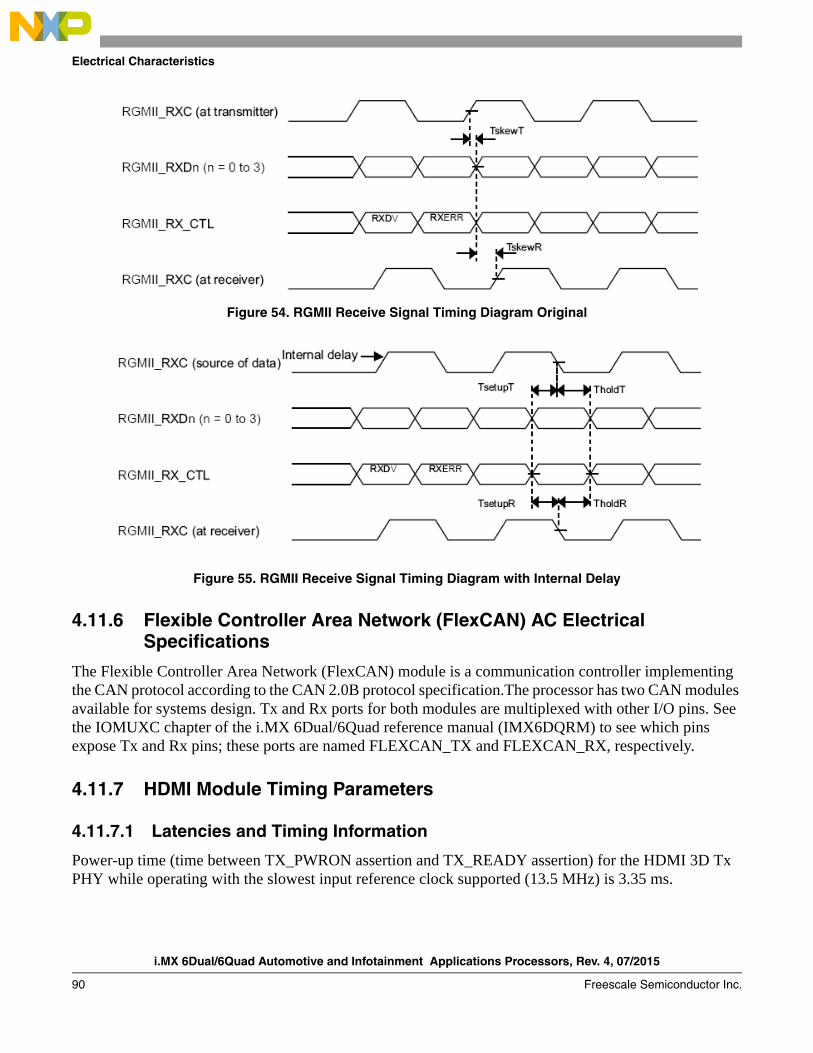
i.MX 6Dual/6Quad Automotive and Infotainment Applications Processors, Rev. 4, 07/2015
90 Freescale Semiconductor Inc.
Electrical Characteristics
Figure 54. RGMII Receive Signal Timing Diagram Original
Figure 55. RGMII Receive Signal Timing Diagram with Internal Delay
4.11.6 Flexible Controller Area Network (FlexCAN) AC Electrical Specifications
The Flexible Controller Area Network (FlexCAN) module is a communication controller implementing the CAN protocol according to the CAN 2.0B protocol specification.The processor has two CAN modules available for systems design. Tx and Rx ports for both modules are multiplexed with other I/O pins. See the IOMUXC chapter of the i.MX 6Dual/6Quad reference manual (IMX6DQRM) to see which pins expose Tx and Rx pins; these ports are named FLEXCAN_TX and FLEXCAN_RX, respectively.
4.11.7 HDMI Module Timing Parameters
4.11.7.1 Latencies and Timing Information
Power-up time (time between TX_PWRON assertion and TX_READY assertion) for the HDMI 3D Tx PHY while operating with the slowest input reference clock supported (13.5 MHz) is 3.35 ms.
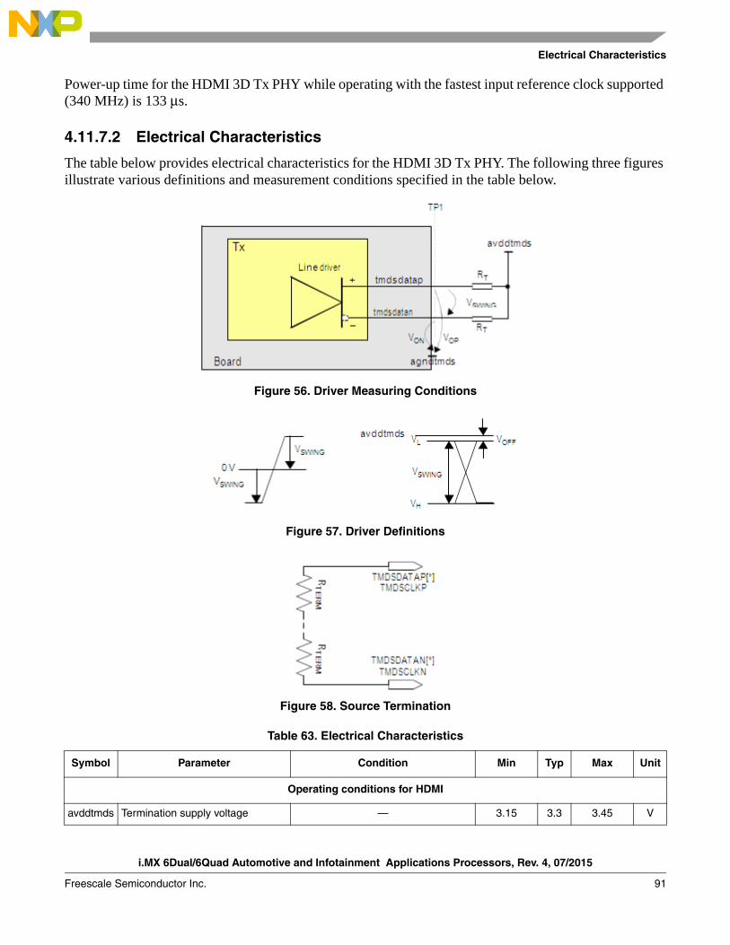
Electrical Characteristics
i.MX 6Dual/6Quad Automotive and Infotainment Applications Processors, Rev. 4, 07/2015
Freescale Semiconductor Inc. 91
Power-up time for the HDMI 3D Tx PHY while operating with the fastest input reference clock supported (340 MHz) is 133 μs.
4.11.7.2 Electrical Characteristics
The table below provides electrical characteristics for the HDMI 3D Tx PHY. The following three figures illustrate various definitions and measurement conditions specified in the table below.
Figure 56. Driver Measuring Conditions
Figure 57. Driver Definitions
Figure 58. Source Termination
Table 63. Electrical Characteristics
Symbol Parameter Condition Min Typ Max Unit
Operating conditions for HDMI
avddtmds Termination supply voltage — 3.15 3.3 3.45 V
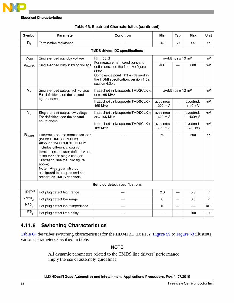
i.MX 6Dual/6Quad Automotive and Infotainment Applications Processors, Rev. 4, 07/2015
92 Freescale Semiconductor Inc.
Electrical Characteristics
4.11.8 Switching Characteristics
Table 64 describes switching characteristics for the HDMI 3D Tx PHY. Figure 59 to Figure 63 illustrate various parameters specified in table.
NOTEAll dynamic parameters related to the TMDS line drivers’ performance imply the use of assembly guidelines.
RT Termination resistance — 45 50 55 Ω
TMDS drivers DC specifications
VOFF Single-ended standby voltage RT = 50 ΩFor measurement conditions and definitions, see the first two figures above.Compliance point TP1 as defined in the HDMI specification, version 1.3a, section 4.2.4.
avddtmds ± 10 mV mV
VSWING Single-ended output swing voltage 400 — 600 mV
VH Single-ended output high voltageFor definition, see the second figure above.
If attached sink supports TMDSCLK < or = 165 MHz
avddtmds ± 10 mV mV
If attached sink supports TMDSCLK > 165 MHz
avddtmds– 200 mV
— avddtmds+ 10 mV
mV
VL Single-ended output low voltageFor definition, see the second figure above.
If attached sink supports TMDSCLK < or = 165 MHz
avddtmds– 600 mV
— avddtmds– 400mV
mV
If attached sink supports TMDSCLK > 165 MHz
avddtmds– 700 mV
— avddtmds– 400 mV
mV
RTERM Differential source termination load (inside HDMI 3D Tx PHY)Although the HDMI 3D Tx PHY includes differential source termination, the user-defined value is set for each single line (for illustration, see the third figure above).Note: RTERM can also be configured to be open and not present on TMDS channels.
— 50 — 200 Ω
Hot plug detect specifications
HPDVH Hot plug detect high range — 2.0 — 5.3 V
VHPDVL Hot plug detect low range — 0 — 0.8 V
HPDZ Hot plug detect input impedance — 10 — — kΩ
HPDt Hot plug detect time delay — — — 100 µs
Table 63. Electrical Characteristics (continued)
Symbol Parameter Condition Min Typ Max Unit
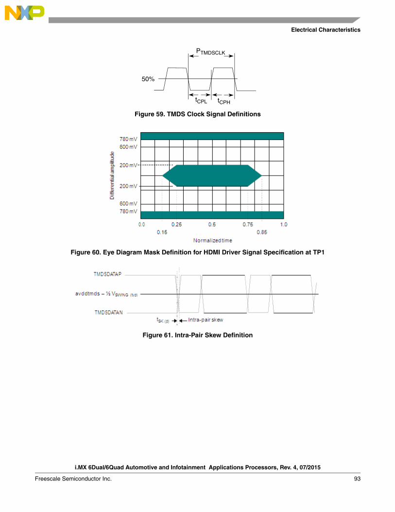
Electrical Characteristics
i.MX 6Dual/6Quad Automotive and Infotainment Applications Processors, Rev. 4, 07/2015
Freescale Semiconductor Inc. 93
Figure 59. TMDS Clock Signal Definitions
Figure 60. Eye Diagram Mask Definition for HDMI Driver Signal Specification at TP1
Figure 61. Intra-Pair Skew Definition
PTMDSCLK
50%
tCPHtCPL
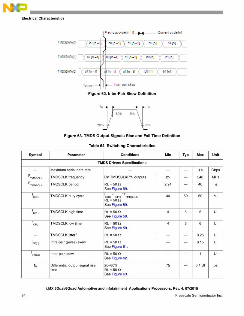
i.MX 6Dual/6Quad Automotive and Infotainment Applications Processors, Rev. 4, 07/2015
94 Freescale Semiconductor Inc.
Electrical Characteristics
Figure 62. Inter-Pair Skew Definition
Figure 63. TMDS Output Signals Rise and Fall Time Definition
Table 64. Switching Characteristics
Symbol Parameter Conditions Min Typ Max Unit
TMDS Drivers Specifications
— Maximum serial data rate — — — 3.4 Gbps
FTMDSCLK TMDSCLK frequency On TMDSCLKP/N outputs 25 — 340 MHz
PTMDSCLK TMDSCLK period RL = 50 Ω
See Figure 59.2.94 — 40 ns
tCDC TMDSCLK duty cycle t
CDC = tCPH / PTMDSCLK
RL = 50 ΩSee Figure 59.
40 50 60 %
tCPH TMDSCLK high time RL = 50 Ω
See Figure 59.4 5 6 UI
tCPL TMDSCLK low time RL = 50 Ω
See Figure 59.4 5 6 UI
— TMDSCLK jitter1 RL = 50 Ω — — 0.25 UI
tSK(p) Intra-pair (pulse) skew RL = 50 Ω
See Figure 61.— — 0.15 UI
tSK(pp) Inter-pair skew RL = 50 Ω
See Figure 62.— — 1 UI
tR Differential output signal rise time
20–80%RL = 50 ΩSee Figure 63.
75 — 0.4 UI ps
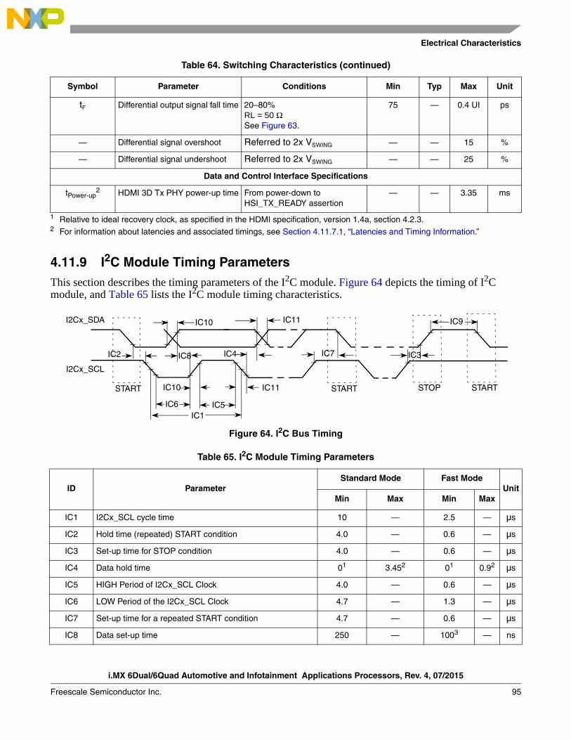
Electrical Characteristics
i.MX 6Dual/6Quad Automotive and Infotainment Applications Processors, Rev. 4, 07/2015
Freescale Semiconductor Inc. 95
4.11.9 I2C Module Timing ParametersThis section describes the timing parameters of the I2C module. Figure 64 depicts the timing of I2C module, and Table 65 lists the I2C module timing characteristics.
Figure 64. I2C Bus Timing
tF Differential output signal fall time 20–80%RL = 50 ΩSee Figure 63.
75 — 0.4 UI ps
— Differential signal overshoot Referred to 2x VSWING — — 15 %
— Differential signal undershoot Referred to 2x VSWING — — 25 %
Data and Control Interface Specifications
tPower-up2 HDMI 3D Tx PHY power-up time From power-down to
HSI_TX_READY assertion— — 3.35 ms
1 Relative to ideal recovery clock, as specified in the HDMI specification, version 1.4a, section 4.2.3.2 For information about latencies and associated timings, see Section 4.11.7.1, “Latencies and Timing Information.”
Table 65. I2C Module Timing Parameters
ID ParameterStandard Mode Fast Mode
UnitMin Max Min Max
IC1 I2Cx_SCL cycle time 10 — 2.5 — µs
IC2 Hold time (repeated) START condition 4.0 — 0.6 — µs
IC3 Set-up time for STOP condition 4.0 — 0.6 — µs
IC4 Data hold time 01 3.452 01 0.92 µs
IC5 HIGH Period of I2Cx_SCL Clock 4.0 — 0.6 — µs
IC6 LOW Period of the I2Cx_SCL Clock 4.7 — 1.3 — µs
IC7 Set-up time for a repeated START condition 4.7 — 0.6 — µs
IC8 Data set-up time 250 — 1003 — ns
Table 64. Switching Characteristics (continued)
Symbol Parameter Conditions Min Typ Max Unit
IC10 IC11 IC9
IC2 IC8 IC4 IC7 IC3
IC6
IC10
IC5
IC11 START STOP STARTSTART
I2Cx_SDA
I2Cx_SCL
IC1
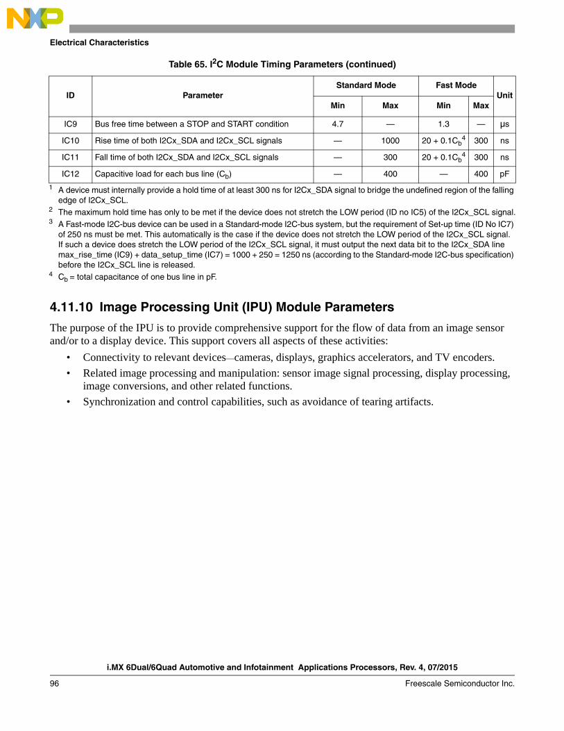
i.MX 6Dual/6Quad Automotive and Infotainment Applications Processors, Rev. 4, 07/2015
96 Freescale Semiconductor Inc.
Electrical Characteristics
4.11.10 Image Processing Unit (IPU) Module Parameters
The purpose of the IPU is to provide comprehensive support for the flow of data from an image sensor and/or to a display device. This support covers all aspects of these activities:
• Connectivity to relevant devices—cameras, displays, graphics accelerators, and TV encoders.
• Related image processing and manipulation: sensor image signal processing, display processing, image conversions, and other related functions.
• Synchronization and control capabilities, such as avoidance of tearing artifacts.
IC9 Bus free time between a STOP and START condition 4.7 — 1.3 — µs
IC10 Rise time of both I2Cx_SDA and I2Cx_SCL signals — 1000 20 + 0.1Cb4 300 ns
IC11 Fall time of both I2Cx_SDA and I2Cx_SCL signals — 300 20 + 0.1Cb4 300 ns
IC12 Capacitive load for each bus line (Cb) — 400 — 400 pF
1 A device must internally provide a hold time of at least 300 ns for I2Cx_SDA signal to bridge the undefined region of the falling edge of I2Cx_SCL.
2 The maximum hold time has only to be met if the device does not stretch the LOW period (ID no IC5) of the I2Cx_SCL signal.3 A Fast-mode I2C-bus device can be used in a Standard-mode I2C-bus system, but the requirement of Set-up time (ID No IC7)
of 250 ns must be met. This automatically is the case if the device does not stretch the LOW period of the I2Cx_SCL signal. If such a device does stretch the LOW period of the I2Cx_SCL signal, it must output the next data bit to the I2Cx_SDA line max_rise_time (IC9) + data_setup_time (IC7) = 1000 + 250 = 1250 ns (according to the Standard-mode I2C-bus specification) before the I2Cx_SCL line is released.
4 Cb = total capacitance of one bus line in pF.
Table 65. I2C Module Timing Parameters (continued)
ID ParameterStandard Mode Fast Mode
UnitMin Max Min Max
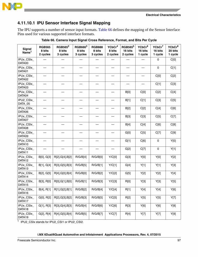
Electrical Characteristics
i.MX 6Dual/6Quad Automotive and Infotainment Applications Processors, Rev. 4, 07/2015
Freescale Semiconductor Inc. 97
4.11.10.1 IPU Sensor Interface Signal Mapping
The IPU supports a number of sensor input formats. Table 66 defines the mapping of the Sensor Interface Pins used for various supported interface formats.
Table 66. Camera Input Signal Cross Reference, Format, and Bits Per Cycle
Signal Name1
1 IPU2_CSIx stands for IPU2_CSI1 or IPU2_CSI2.
RGB5658 bits
2 cycles
RGB5652
8 bits3 cycles
RGB6663
8 bits3 cycles
RGB8888 bits
3 cycles
YCbCr4
8 bits2 cycles
RGB5655
16 bits2 cycles
YCbCr6
16 bits1 cycle
YCbCr7
16 bits1 cycle
YCbCr8
20 bits1 cycle
IPUx_CSIx_DATA00
— — — — — — — 0 C[0]
IPUx_CSIx_DATA01
— — — — — — — 0 C[1]
IPUx_CSIx_DATA02
— — — — — — — C[0] C[2]
IPUx_CSIx_DATA03
— — — — — — — C[1] C[3]
IPUx_CSIx_DATA04
— — — — — B[0] C[0] C[2] C[4]
IPU2_CSIx_DATA_05
— — — — — B[1] C[1] C[3] C[5]
IPUx_CSIx_DATA06
— — — — — B[2] C[2] C[4] C[6]
IPUx_CSIx_DATA07
— — — — — B[3] C[3] C[5] C[7]
IPUx_CSIx_DATA08
— — — — — B[4] C[4] C[6] C[8]
IPUx_CSIx_DATA09
— — — — — G[0] C[5] C[7] C[9]
IPUx_CSIx_DATA10
— — — — — G[1] C[6] 0 Y[0]
IPUx_CSIx_DATA11
— — — — — G[2] C[7] 0 Y[1]
IPUx_CSIx_DATA12
B[0], G[3] R[2],G[4],B[2] R/G/B[4] R/G/B[0] Y/C[0] G[3] Y[0] Y[0] Y[2]
IPUx_CSIx_DATA13
B[1], G[4] R[3],G[5],B[3] R/G/B[5] R/G/B[1] Y/C[1] G[4] Y[1] Y[1] Y[3]
IPUx_CSIx_DATA14
B[2], G[5] R[4],G[0],B[4] R/G/B[0] R/G/B[2] Y/C[2] G[5] Y[2] Y[2] Y[4]
IPUx_CSIx_DATA15
B[3], R[0] R[0],G[1],B[0] R/G/B[1] R/G/B[3] Y/C[3] R[0] Y[3] Y[3] Y[5]
IPUx_CSIx_DATA16
B[4], R[1] R[1],G[2],B[1] R/G/B[2] R/G/B[4] Y/C[4] R[1] Y[4] Y[4] Y[6]
IPUx_CSIx_DATA17
G[0], R[2] R[2],G[3],B[2] R/G/B[3] R/G/B[5] Y/C[5] R[2] Y[5] Y[5] Y[7]
IPUx_CSIx_DATA18
G[1], R[3] R[3],G[4],B[3] R/G/B[4] R/G/B[6] Y/C[6] R[3] Y[6] Y[6] Y[8]
IPUx_CSIx_DATA19
G[2], R[4] R[4],G[5],B[4] R/G/B[5] R/G/B[7] Y/C[7] R[4] Y[7] Y[7] Y[9]
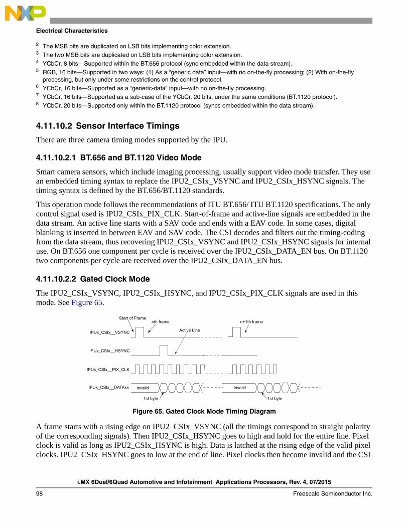
i.MX 6Dual/6Quad Automotive and Infotainment Applications Processors, Rev. 4, 07/2015
98 Freescale Semiconductor Inc.
Electrical Characteristics
4.11.10.2 Sensor Interface Timings
There are three camera timing modes supported by the IPU.
4.11.10.2.1 BT.656 and BT.1120 Video Mode
Smart camera sensors, which include imaging processing, usually support video mode transfer. They use an embedded timing syntax to replace the IPU2_CSIx_VSYNC and IPU2_CSIx_HSYNC signals. The timing syntax is defined by the BT.656/BT.1120 standards.
This operation mode follows the recommendations of ITU BT.656/ ITU BT.1120 specifications. The only control signal used is IPU2_CSIx_PIX_CLK. Start-of-frame and active-line signals are embedded in the data stream. An active line starts with a SAV code and ends with a EAV code. In some cases, digital blanking is inserted in between EAV and SAV code. The CSI decodes and filters out the timing-coding from the data stream, thus recovering IPU2_CSIx_VSYNC and IPU2_CSIx_HSYNC signals for internal use. On BT.656 one component per cycle is received over the IPU2_CSIx_DATA_EN bus. On BT.1120 two components per cycle are received over the IPU2_CSIx_DATA_EN bus.
4.11.10.2.2 Gated Clock Mode
The IPU2_CSIx_VSYNC, IPU2_CSIx_HSYNC, and IPU2_CSIx_PIX_CLK signals are used in this mode. See Figure 65.
Figure 65. Gated Clock Mode Timing Diagram
A frame starts with a rising edge on IPU2_CSIx_VSYNC (all the timings correspond to straight polarity of the corresponding signals). Then IPU2_CSIx_HSYNC goes to high and hold for the entire line. Pixel clock is valid as long as IPU2_CSIx_HSYNC is high. Data is latched at the rising edge of the valid pixel clocks. IPU2_CSIx_HSYNC goes to low at the end of line. Pixel clocks then become invalid and the CSI
2 The MSB bits are duplicated on LSB bits implementing color extension.3 The two MSB bits are duplicated on LSB bits implementing color extension.4 YCbCr, 8 bits—Supported within the BT.656 protocol (sync embedded within the data stream).5 RGB, 16 bits—Supported in two ways: (1) As a “generic data” input—with no on-the-fly processing; (2) With on-the-fly
processing, but only under some restrictions on the control protocol.6 YCbCr, 16 bits—Supported as a “generic-data” input—with no on-the-fly processing.7 YCbCr, 16 bits—Supported as a sub-case of the YCbCr, 20 bits, under the same conditions (BT.1120 protocol).8 YCbCr, 20 bits—Supported only within the BT.1120 protocol (syncs embedded within the data stream).
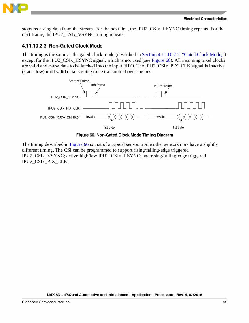
Electrical Characteristics
i.MX 6Dual/6Quad Automotive and Infotainment Applications Processors, Rev. 4, 07/2015
Freescale Semiconductor Inc. 99
stops receiving data from the stream. For the next line, the IPU2_CSIx_HSYNC timing repeats. For the next frame, the IPU2_CSIx_VSYNC timing repeats.
4.11.10.2.3 Non-Gated Clock Mode
The timing is the same as the gated-clock mode (described in Section 4.11.10.2.2, “Gated Clock Mode,”) except for the IPU2_CSIx_HSYNC signal, which is not used (see Figure 66). All incoming pixel clocks are valid and cause data to be latched into the input FIFO. The IPU2_CSIx_PIX_CLK signal is inactive (states low) until valid data is going to be transmitted over the bus.
Figure 66. Non-Gated Clock Mode Timing Diagram
The timing described in Figure 66 is that of a typical sensor. Some other sensors may have a slightly different timing. The CSI can be programmed to support rising/falling-edge triggered IPU2_CSIx_VSYNC; active-high/low IPU2_CSIx_HSYNC; and rising/falling-edge triggered IPU2_CSIx_PIX_CLK.
IPU2_CSIx_VSYNC
IPU2_CSIx_PIX_CLK
IPU2_CSIx_DATA_EN[19:0] invalid
1st byte
n+1th frame
invalid
1st byte
nth frameStart of Frame
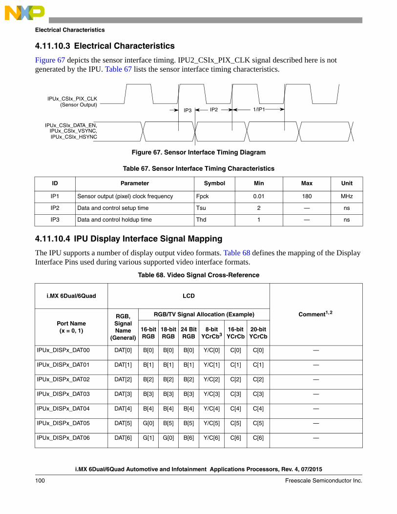
i.MX 6Dual/6Quad Automotive and Infotainment Applications Processors, Rev. 4, 07/2015
100 Freescale Semiconductor Inc.
Electrical Characteristics
4.11.10.3 Electrical Characteristics
Figure 67 depicts the sensor interface timing. IPU2_CSIx_PIX_CLK signal described here is not generated by the IPU. Table 67 lists the sensor interface timing characteristics.
Figure 67. Sensor Interface Timing Diagram
4.11.10.4 IPU Display Interface Signal Mapping
The IPU supports a number of display output video formats. Table 68 defines the mapping of the Display Interface Pins used during various supported video interface formats.
Table 67. Sensor Interface Timing Characteristics
ID Parameter Symbol Min Max Unit
IP1 Sensor output (pixel) clock frequency Fpck 0.01 180 MHz
IP2 Data and control setup time Tsu 2 — ns
IP3 Data and control holdup time Thd 1 — ns
Table 68. Video Signal Cross-Reference
i.MX 6Dual/6Quad LCD
Comment1,2
Port Name(x = 0, 1)
RGB,SignalName
(General)
RGB/TV Signal Allocation (Example)
16-bitRGB
18-bitRGB
24 BitRGB
8-bitYCrCb3
16-bitYCrCb
20-bitYCrCb
IPUx_DISPx_DAT00 DAT[0] B[0] B[0] B[0] Y/C[0] C[0] C[0] —
IPUx_DISPx_DAT01 DAT[1] B[1] B[1] B[1] Y/C[1] C[1] C[1] —
IPUx_DISPx_DAT02 DAT[2] B[2] B[2] B[2] Y/C[2] C[2] C[2] —
IPUx_DISPx_DAT03 DAT[3] B[3] B[3] B[3] Y/C[3] C[3] C[3] —
IPUx_DISPx_DAT04 DAT[4] B[4] B[4] B[4] Y/C[4] C[4] C[4] —
IPUx_DISPx_DAT05 DAT[5] G[0] B[5] B[5] Y/C[5] C[5] C[5] —
IPUx_DISPx_DAT06 DAT[6] G[1] G[0] B[6] Y/C[6] C[6] C[6] —
IP3
IPUx_CSIx_DATA_EN,IPUx_CSIx_VSYNC,
IP2 1/IP1
IPUx_CSIx_PIX_CLK(Sensor Output)
IPUx_CSIx_HSYNC
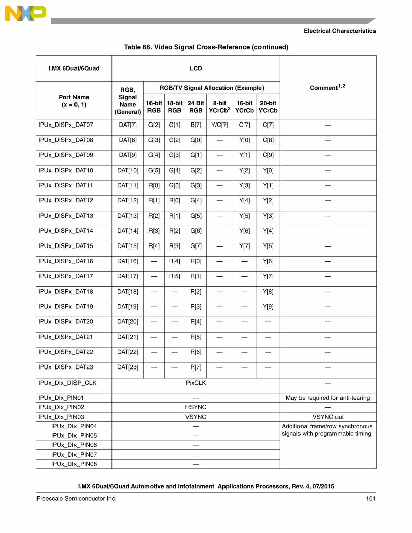
Electrical Characteristics
i.MX 6Dual/6Quad Automotive and Infotainment Applications Processors, Rev. 4, 07/2015
Freescale Semiconductor Inc. 101
IPUx_DISPx_DAT07 DAT[7] G[2] G[1] B[7] Y/C[7] C[7] C[7] —
IPUx_DISPx_DAT08 DAT[8] G[3] G[2] G[0] — Y[0] C[8] —
IPUx_DISPx_DAT09 DAT[9] G[4] G[3] G[1] — Y[1] C[9] —
IPUx_DISPx_DAT10 DAT[10] G[5] G[4] G[2] — Y[2] Y[0] —
IPUx_DISPx_DAT11 DAT[11] R[0] G[5] G[3] — Y[3] Y[1] —
IPUx_DISPx_DAT12 DAT[12] R[1] R[0] G[4] — Y[4] Y[2] —
IPUx_DISPx_DAT13 DAT[13] R[2] R[1] G[5] — Y[5] Y[3] —
IPUx_DISPx_DAT14 DAT[14] R[3] R[2] G[6] — Y[6] Y[4] —
IPUx_DISPx_DAT15 DAT[15] R[4] R[3] G[7] — Y[7] Y[5] —
IPUx_DISPx_DAT16 DAT[16] — R[4] R[0] — — Y[6] —
IPUx_DISPx_DAT17 DAT[17] — R[5] R[1] — — Y[7] —
IPUx_DISPx_DAT18 DAT[18] — — R[2] — — Y[8] —
IPUx_DISPx_DAT19 DAT[19] — — R[3] — — Y[9] —
IPUx_DISPx_DAT20 DAT[20] — — R[4] — — — —
IPUx_DISPx_DAT21 DAT[21] — — R[5] — — — —
IPUx_DISPx_DAT22 DAT[22] — — R[6] — — — —
IPUx_DISPx_DAT23 DAT[23] — — R[7] — — — —
IPUx_DIx_DISP_CLK PixCLK —
IPUx_DIx_PIN01 — May be required for anti-tearing
IPUx_DIx_PIN02 HSYNC —
IPUx_DIx_PIN03 VSYNC VSYNC out
IPUx_DIx_PIN04 — Additional frame/row synchronous signals with programmable timingIPUx_DIx_PIN05 —
IPUx_DIx_PIN06 —
IPUx_DIx_PIN07 —
IPUx_DIx_PIN08 —
Table 68. Video Signal Cross-Reference (continued)
i.MX 6Dual/6Quad LCD
Comment1,2
Port Name(x = 0, 1)
RGB,SignalName
(General)
RGB/TV Signal Allocation (Example)
16-bitRGB
18-bitRGB
24 BitRGB
8-bitYCrCb3
16-bitYCrCb
20-bitYCrCb
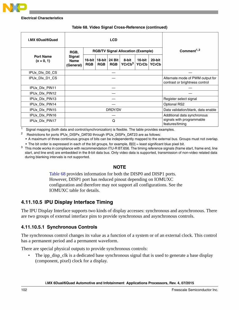
i.MX 6Dual/6Quad Automotive and Infotainment Applications Processors, Rev. 4, 07/2015
102 Freescale Semiconductor Inc.
Electrical Characteristics
NOTETable 68 provides information for both the DISP0 and DISP1 ports. However, DISP1 port has reduced pinout depending on IOMUXC configuration and therefore may not support all configurations. See the IOMUXC table for details.
4.11.10.5 IPU Display Interface Timing
The IPU Display Interface supports two kinds of display accesses: synchronous and asynchronous. There are two groups of external interface pins to provide synchronous and asynchronous controls.
4.11.10.5.1 Synchronous Controls
The synchronous control changes its value as a function of a system or of an external clock. This control has a permanent period and a permanent waveform.
There are special physical outputs to provide synchronous controls:
• The ipp_disp_clk is a dedicated base synchronous signal that is used to generate a base display (component, pixel) clock for a display.
IPUx_DIx_D0_CS — —
IPUx_DIx_D1_CS — Alternate mode of PWM output for contrast or brightness control
IPUx_DIx_PIN11 — —
IPUx_DIx_PIN12 — —
IPUx_DIx_PIN13 — Register select signal
IPUx_DIx_PIN14 — Optional RS2
IPUx_DIx_PIN15 DRDY/DV Data validation/blank, data enable
IPUx_DIx_PIN16 — Additional data synchronous signals with programmable features/timing
IPUx_DIx_PIN17 Q
1 Signal mapping (both data and control/synchronization) is flexible. The table provides examples.2 Restrictions for ports IPUx_DISPx_DAT00 through IPUx_DISPx_DAT23 are as follows:
• A maximum of three continuous groups of bits can be independently mapped to the external bus. Groups must not overlap.
• The bit order is expressed in each of the bit groups, for example, B[0] = least significant blue pixel bit.3 This mode works in compliance with recommendation ITU-R BT.656. The timing reference signals (frame start, frame end, line
start, and line end) are embedded in the 8-bit data bus. Only video data is supported, transmission of non-video related data during blanking intervals is not supported.
Table 68. Video Signal Cross-Reference (continued)
i.MX 6Dual/6Quad LCD
Comment1,2
Port Name(x = 0, 1)
RGB,SignalName
(General)
RGB/TV Signal Allocation (Example)
16-bitRGB
18-bitRGB
24 BitRGB
8-bitYCrCb3
16-bitYCrCb
20-bitYCrCb
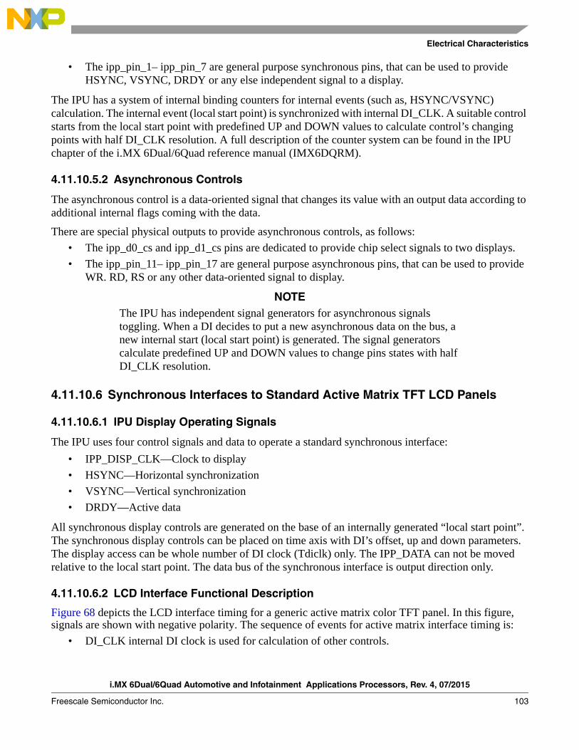
Electrical Characteristics
i.MX 6Dual/6Quad Automotive and Infotainment Applications Processors, Rev. 4, 07/2015
Freescale Semiconductor Inc. 103
• The ipp_pin_1– ipp_pin_7 are general purpose synchronous pins, that can be used to provide HSYNC, VSYNC, DRDY or any else independent signal to a display.
The IPU has a system of internal binding counters for internal events (such as, HSYNC/VSYNC) calculation. The internal event (local start point) is synchronized with internal DI_CLK. A suitable control starts from the local start point with predefined UP and DOWN values to calculate control’s changing points with half DI_CLK resolution. A full description of the counter system can be found in the IPU chapter of the i.MX 6Dual/6Quad reference manual (IMX6DQRM).
4.11.10.5.2 Asynchronous Controls
The asynchronous control is a data-oriented signal that changes its value with an output data according to additional internal flags coming with the data.
There are special physical outputs to provide asynchronous controls, as follows:
• The ipp_d0_cs and ipp_d1_cs pins are dedicated to provide chip select signals to two displays.
• The ipp_pin_11– ipp_pin_17 are general purpose asynchronous pins, that can be used to provide WR. RD, RS or any other data-oriented signal to display.
NOTEThe IPU has independent signal generators for asynchronous signals toggling. When a DI decides to put a new asynchronous data on the bus, a new internal start (local start point) is generated. The signal generators calculate predefined UP and DOWN values to change pins states with half DI_CLK resolution.
4.11.10.6 Synchronous Interfaces to Standard Active Matrix TFT LCD Panels
4.11.10.6.1 IPU Display Operating Signals
The IPU uses four control signals and data to operate a standard synchronous interface:
• IPP_DISP_CLK—Clock to display
• HSYNC—Horizontal synchronization
• VSYNC—Vertical synchronization
• DRDY—Active data
All synchronous display controls are generated on the base of an internally generated “local start point”. The synchronous display controls can be placed on time axis with DI’s offset, up and down parameters. The display access can be whole number of DI clock (Tdiclk) only. The IPP_DATA can not be moved relative to the local start point. The data bus of the synchronous interface is output direction only.
4.11.10.6.2 LCD Interface Functional Description
Figure 68 depicts the LCD interface timing for a generic active matrix color TFT panel. In this figure, signals are shown with negative polarity. The sequence of events for active matrix interface timing is:
• DI_CLK internal DI clock is used for calculation of other controls.
i.MX 6Dual/6Quad Automotive and Infotainment Applications Processors, Rev. 4, 07/2015
104 Freescale Semiconductor Inc.
Electrical Characteristics
• IPP_DISP_CLK latches data into the panel on its negative edge (when positive polarity is selected). In active mode, IPP_DISP_CLK runs continuously.
• HSYNC causes the panel to start a new line. (Usually IPUx_DIx_PIN02 is used as HSYNC.)
• VSYNC causes the panel to start a new frame. It always encompasses at least one HSYNC pulse. (Usually IPUx_DIx_PIN03 is used as VSYNC.)
• DRDY acts like an output enable signal to the CRT display. This output enables the data to be shifted onto the display. When disabled, the data is invalid and the trace is off. (DRDY can be used either synchronous or asynchronous generic purpose pin as well.)
Figure 68. Interface Timing Diagram for TFT (Active Matrix) Panels
4.11.10.6.3 TFT Panel Sync Pulse Timing Diagrams
Figure 69 depicts the horizontal timing (timing of one line), including both the horizontal sync pulse and the data. All the parameters shown in the figure are programmable. All controls are started by corresponding internal events—local start points. The timing diagrams correspond to inverse polarity of the IPP_DISP_CLK signal and active-low polarity of the HSYNC, VSYNC, and DRDY signals.
1 2 3 mm–1
HSYNC
VSYNC
HSYNC
LINE 1 LINE 2 LINE 3 LINE 4 LINE n-1 LINE n
DRDY
IPP_DISP_CLK
IPP_DATA
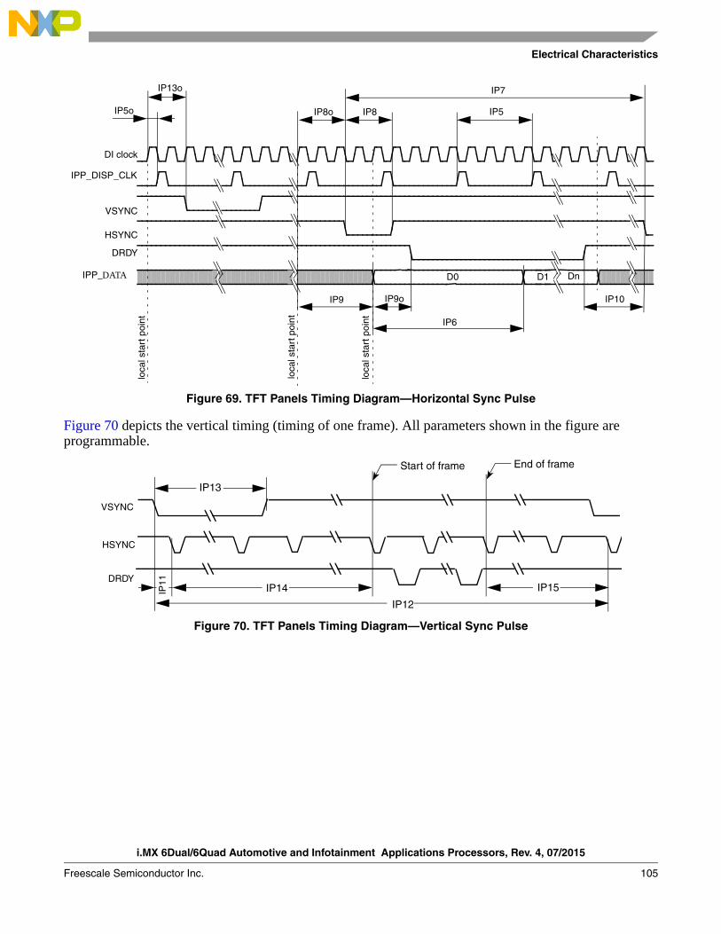
Electrical Characteristics
i.MX 6Dual/6Quad Automotive and Infotainment Applications Processors, Rev. 4, 07/2015
Freescale Semiconductor Inc. 105
Figure 69. TFT Panels Timing Diagram—Horizontal Sync Pulse
Figure 70 depicts the vertical timing (timing of one frame). All parameters shown in the figure are programmable.
Figure 70. TFT Panels Timing Diagram—Vertical Sync Pulse
DI clock
VSYNC
HSYNC
DRDY
D0 D1
IP5o
IP13o
IP9o
IP8o IP8
IP9
Dn
IP10
IP7
IP5
IP6
loca
l sta
rt p
oint
loca
l sta
rt p
oint
loca
l sta
rt p
oint
IPP_DISP_CLK
IPP_DATA
IP14
VSYNC
HSYNC
DRDY
Start of frame End of frame
IP12
IP15
IP13
IP11
i.MX 6Dual/6Quad Automotive and Infotainment Applications Processors, Rev. 4, 07/2015
106 Freescale Semiconductor Inc.
Electrical Characteristics
Table 69 shows timing characteristics of signals presented in Figure 69 and Figure 70.
Table 69. Synchronous Display Interface Timing Characteristics (Pixel Level)
ID Parameter Symbol Value Description Unit
IP5 Display interface clock period Tdicp (see1) Display interface clock IPP_DISP_CLK ns
IP6 Display pixel clock period Tdpcp DISP_CLK_PER_PIXEL× Tdicp
Time of translation of one pixel to display, DISP_CLK_PER_PIXEL—number of pixel components in one pixel (1.n). The DISP_CLK_PER_PIXEL is virtual parameter to define display pixel clock period.The DISP_CLK_PER_PIXEL is received by DC/DI one access division to n components.
ns
IP7 Screen width time Tsw (SCREEN_WIDTH)× Tdicp
SCREEN_WIDTH—screen width in, interface clocks. horizontal blanking included.The SCREEN_WIDTH should be built by suitable DI’s counter2.
ns
IP8 HSYNC width time Thsw (HSYNC_WIDTH) HSYNC_WIDTH—Hsync width in DI_CLK with 0.5 DI_CLK resolution. Defined by DI’s counter.
ns
IP9 Horizontal blank interval 1 Thbi1 BGXP × Tdicp BGXP—width of a horizontal blanking before a first active data in a line (in interface clocks). The BGXP should be built by suitable DI’s counter.
ns
IP10 Horizontal blank interval 2 Thbi2 (SCREEN_WIDTH – BGXP – FW) × Tdicp
Width a horizontal blanking after a last active data in a line (in interface clocks) FW—with of active line in interface clocks. The FW should be built by suitable DI’s counter.
ns
IP12 Screen height Tsh (SCREEN_HEIGHT)× Tsw
SCREEN_HEIGHT— screen height in lines with blanking.The SCREEN_HEIGHT is a distance between 2 VSYNCs.The SCREEN_HEIGHT should be built by suitable DI’s counter.
ns
IP13 VSYNC width Tvsw VSYNC_WIDTH VSYNC_WIDTH—Vsync width in DI_CLK with 0.5 DI_CLK resolution. Defined by DI’s counter.
ns
IP14 Vertical blank interval 1 Tvbi1 BGYP × Tsw BGYP—width of first Verticalblanking interval in line. The BGYP should be built by suitable DI’s counter.
ns
IP15 Vertical blank interval 2 Tvbi2 (SCREEN_HEIGHT – BGYP – FH) × Tsw
Width of second vertical blanking interval in line. The FH should be built by suitable DI’s counter.
ns
Electrical Characteristics
i.MX 6Dual/6Quad Automotive and Infotainment Applications Processors, Rev. 4, 07/2015
Freescale Semiconductor Inc. 107
The maximum accuracy of UP/DOWN edge of controls is:
IP5o Offset of IPP_DISP_CLK Todicp DISP_CLK_OFFSET× Tdiclk
DISP_CLK_OFFSET—offset of IPP_DISP_CLK edges from local start point, in DI_CLK×2 (0.5 DI_CLK Resolution).Defined by DISP_CLK counter.
ns
IP13o Offset of VSYNC Tovs VSYNC_OFFSET× Tdiclk
VSYNC_OFFSET—offset of Vsync edges from a local start point, when a Vsync should be active, in DI_CLK×2 (0.5 DI_CLK Resolution). The VSYNC_OFFSET should be built by suitable DI’s counter.
ns
IP8o Offset of HSYNC Tohs HSYNC_OFFSET× Tdiclk
HSYNC_OFFSET—offset of Hsync edges from a local start point, when a Hsync should be active, in DI_CLK×2 (0.5 DI_CLK Resolution). The HSYNC_OFFSET should be built by suitable DI’s counter.
ns
IP9o Offset of DRDY Todrdy DRDY_OFFSET× Tdiclk
DRDY_OFFSET—offset of DRDY edges from a suitable local start point, when a corresponding data has been set on the bus, in DI_CLK×2 (0.5 DI_CLK Resolution).The DRDY_OFFSET should be built by suitable DI’s counter.
ns
1 Display interface clock period immediate value.
DISP_CLK_PERIOD—number of DI_CLK per one Tdicp. Resolution 1/16 of DI_CLK.DI_CLK_PERIOD—relation of between programing clock frequency and current system clock frequencyDisplay interface clock period average value.
2 DI’s counter can define offset, period and UP/DOWN characteristic of output signal according to programed parameters of the counter. Same of parameters in the table are not defined by DI’s registers directly (by name), but can be generated by corresponding DI’s counter. The SCREEN_WIDTH is an input value for DI’s HSYNC generation counter. The distance between HSYNCs is a SCREEN_WIDTH.
Table 69. Synchronous Display Interface Timing Characteristics (Pixel Level) (continued)
ID Parameter Symbol Value Description Unit
Tdicp
TdiclkDISP_CLK_PERIOD
DI_CLK_PERIOD----------------------------------------------------× for integer DISP_CLK_PERIOD
DI_CLK_PERIOD----------------------------------------------------,
Tdiclk floor DISP_CLK_PERIODDI_CLK_PERIOD
---------------------------------------------------- 0.5 0.5±+ for fractional DISP_CLK_PERIOD
DI_CLK_PERIOD----------------------------------------------------,
=
Tdicp TdiclkDISP_CLK_PERIOD
DI_CLK_PERIOD----------------------------------------------------×=
Accuracy 0.5 Tdiclk×( ) 0.62ns±=
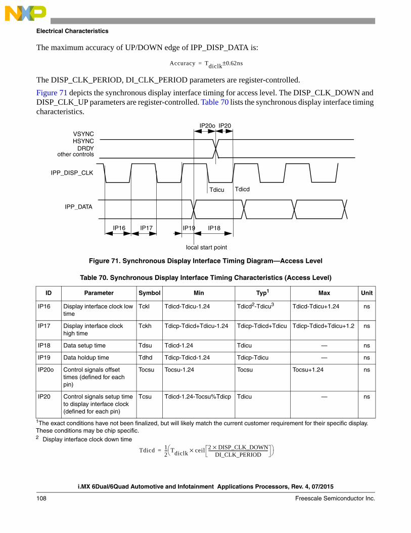
i.MX 6Dual/6Quad Automotive and Infotainment Applications Processors, Rev. 4, 07/2015
108 Freescale Semiconductor Inc.
Electrical Characteristics
The maximum accuracy of UP/DOWN edge of IPP_DISP_DATA is:
The DISP_CLK_PERIOD, DI_CLK_PERIOD parameters are register-controlled.
Figure 71 depicts the synchronous display interface timing for access level. The DISP_CLK_DOWN and DISP_CLK_UP parameters are register-controlled. Table 70 lists the synchronous display interface timing characteristics.
Figure 71. Synchronous Display Interface Timing Diagram—Access Level
Table 70. Synchronous Display Interface Timing Characteristics (Access Level)
ID Parameter Symbol Min Typ1
1The exact conditions have not been finalized, but will likely match the current customer requirement for their specific display. These conditions may be chip specific.
Max Unit
IP16 Display interface clock low time
Tckl Tdicd-Tdicu-1.24 Tdicd2-Tdicu3
2 Display interface clock down time
Tdicd-Tdicu+1.24 ns
IP17 Display interface clock high time
Tckh Tdicp-Tdicd+Tdicu-1.24 Tdicp-Tdicd+Tdicu Tdicp-Tdicd+Tdicu+1.2 ns
IP18 Data setup time Tdsu Tdicd-1.24 Tdicu — ns
IP19 Data holdup time Tdhd Tdicp-Tdicd-1.24 Tdicp-Tdicu — ns
IP20o Control signals offset times (defined for each pin)
Tocsu Tocsu-1.24 Tocsu Tocsu+1.24 ns
IP20 Control signals setup time to display interface clock (defined for each pin)
Tcsu Tdicd-1.24-Tocsu%Tdicp Tdicu — ns
Accuracy Tdiclk 0.62ns±=
IP19 IP18
IP20VSYNC
IP17IP16
DRDYHSYNC
other controls
IP20o
local start point
TdicdTdicu
IPP_DISP_CLK
IPP_DATA
Tdicd 12--- Tdiclk ceil× 2 DISP_CLK_DOWN×
DI_CLK_PERIOD-----------------------------------------------------------
=
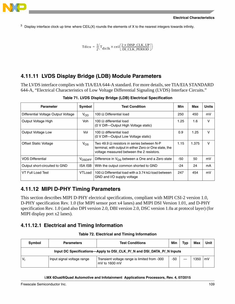
Electrical Characteristics
i.MX 6Dual/6Quad Automotive and Infotainment Applications Processors, Rev. 4, 07/2015
Freescale Semiconductor Inc. 109
4.11.11 LVDS Display Bridge (LDB) Module Parameters
The LVDS interface complies with TIA/EIA 644-A standard. For more details, see TIA/EIA STANDARD 644-A, “Electrical Characteristics of Low Voltage Differential Signaling (LVDS) Interface Circuits.”
4.11.12 MIPI D-PHY Timing Parameters
This section describes MIPI D-PHY electrical specifications, compliant with MIPI CSI-2 version 1.0, D-PHY specification Rev. 1.0 (for MIPI sensor port x4 lanes) and MIPI DSI Version 1.01, and D-PHY specification Rev. 1.0 (and also DPI version 2.0, DBI version 2.0, DSC version 1.0a at protocol layer) (for MIPI display port x2 lanes).
4.11.12.1 Electrical and Timing Information
3 Display interface clock up time where CEIL(X) rounds the elements of X to the nearest integers towards infinity.
Table 71. LVDS Display Bridge (LDB) Electrical Specification
Parameter Symbol Test Condition Min Max Units
Differential Voltage Output Voltage VOD 100 Ω Differential load 250 450 mV
Output Voltage High Voh 100 Ω differential load (0 V Diff—Output High Voltage static)
1.25 1.6 V
Output Voltage Low Vol 100 Ω differential load(0 V Diff—Output Low Voltage static)
0.9 1.25 V
Offset Static Voltage VOS Two 49.9 Ω resistors in series between N-P terminal, with output in either Zero or One state, the voltage measured between the 2 resistors.
1.15 1.375 V
VOS Differential VOSDIFF Difference in VOS between a One and a Zero state -50 50 mV
Output short-circuited to GND ISA ISB With the output common shorted to GND -24 24 mA
VT Full Load Test VTLoad 100 Ω Differential load with a 3.74 kΩ load between GND and I/O supply voltage
247 454 mV
Table 72. Electrical and Timing Information
Symbol Parameters Test Conditions Min Typ Max Unit
Input DC Specifications—Apply to DSI_CLK_P/_N and DSI_DATA_P/_N Inputs
VI Input signal voltage range Transient voltage range is limited from -300 mV to 1600 mV
-50 — 1350 mV
Tdicu 12--- Tdiclk ceil× 2 DISP_CLK_UP×
DI_CLK_PERIOD------------------------------------------------
=
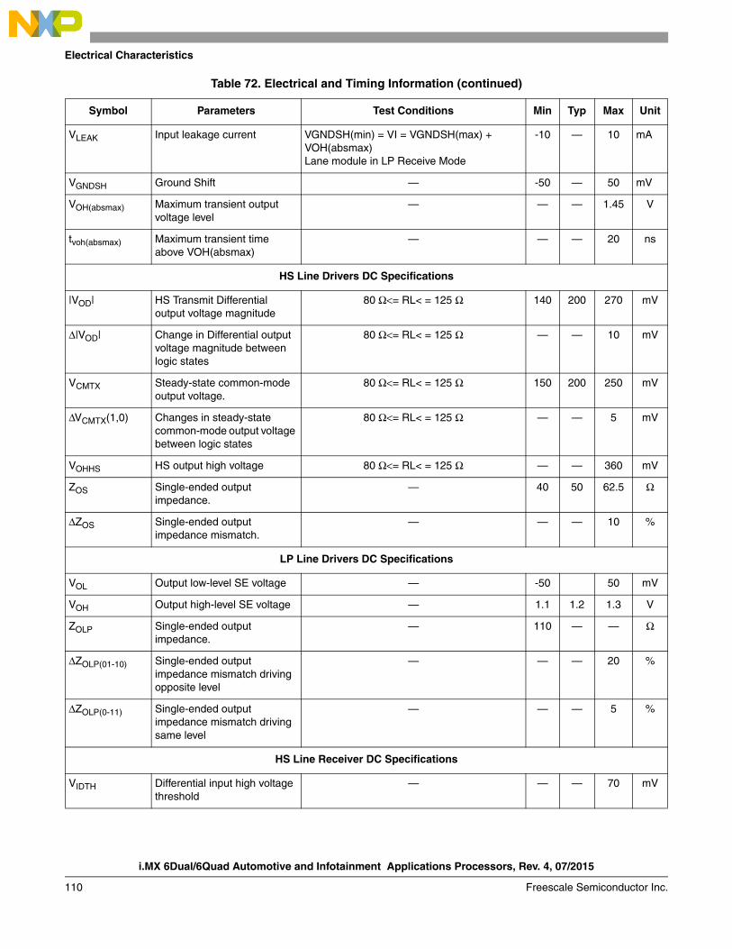
i.MX 6Dual/6Quad Automotive and Infotainment Applications Processors, Rev. 4, 07/2015
110 Freescale Semiconductor Inc.
Electrical Characteristics
VLEAK Input leakage current VGNDSH(min) = VI = VGNDSH(max) + VOH(absmax)Lane module in LP Receive Mode
-10 — 10 mA
VGNDSH Ground Shift — -50 — 50 mV
VOH(absmax) Maximum transient output voltage level
— — — 1.45 V
tvoh(absmax) Maximum transient time above VOH(absmax)
— — — 20 ns
HS Line Drivers DC Specifications
|VOD| HS Transmit Differential output voltage magnitude
80 Ω<= RL< = 125 Ω 140 200 270 mV
Δ|VOD| Change in Differential output voltage magnitude between logic states
80 Ω<= RL< = 125 Ω — — 10 mV
VCMTX Steady-state common-mode output voltage.
80 Ω<= RL< = 125 Ω 150 200 250 mV
ΔVCMTX(1,0) Changes in steady-state common-mode output voltage between logic states
80 Ω<= RL< = 125 Ω — — 5 mV
VOHHS HS output high voltage 80 Ω<= RL< = 125 Ω — — 360 mV
ZOS Single-ended output impedance.
— 40 50 62.5 Ω
ΔZOS Single-ended output impedance mismatch.
— — — 10 %
LP Line Drivers DC Specifications
VOL Output low-level SE voltage — -50 50 mV
VOH Output high-level SE voltage — 1.1 1.2 1.3 V
ZOLP Single-ended output impedance.
— 110 — — Ω
ΔZOLP(01-10) Single-ended output impedance mismatch driving opposite level
— — — 20 %
ΔZOLP(0-11) Single-ended output impedance mismatch driving same level
— — — 5 %
HS Line Receiver DC Specifications
VIDTH Differential input high voltage threshold
— — — 70 mV
Table 72. Electrical and Timing Information (continued)
Symbol Parameters Test Conditions Min Typ Max Unit
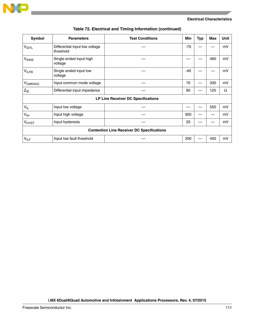
Electrical Characteristics
i.MX 6Dual/6Quad Automotive and Infotainment Applications Processors, Rev. 4, 07/2015
Freescale Semiconductor Inc. 111
VIDTL Differential input low voltage threshold
— -70 — — mV
VIHHS Single ended input high voltage
— — — 460 mV
VILHS Single ended input low voltage
— -40 — — mV
VCMRXDC Input common mode voltage — 70 — 330 mV
ZID Differential input impedance — 80 — 125 Ω
LP Line Receiver DC Specifications
VIL Input low voltage — — — 550 mV
VIH Input high voltage — 920 — — mV
VHYST Input hysteresis — 25 — — mV
Contention Line Receiver DC Specifications
VILF Input low fault threshold — 200 — 450 mV
Table 72. Electrical and Timing Information (continued)
Symbol Parameters Test Conditions Min Typ Max Unit
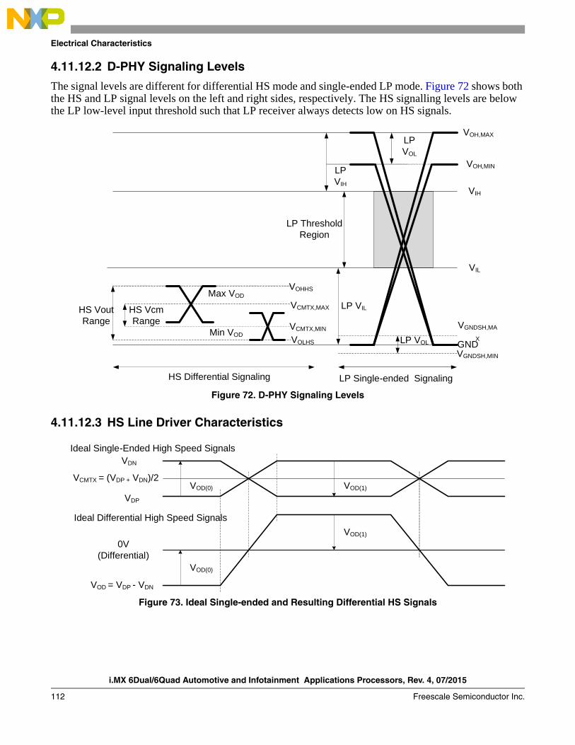
i.MX 6Dual/6Quad Automotive and Infotainment Applications Processors, Rev. 4, 07/2015
112 Freescale Semiconductor Inc.
Electrical Characteristics
4.11.12.2 D-PHY Signaling Levels
The signal levels are different for differential HS mode and single-ended LP mode. Figure 72 shows both the HS and LP signal levels on the left and right sides, respectively. The HS signalling levels are below the LP low-level input threshold such that LP receiver always detects low on HS signals.
Figure 72. D-PHY Signaling Levels
4.11.12.3 HS Line Driver Characteristics
Figure 73. Ideal Single-ended and Resulting Differential HS Signals
HS Vout Range
HS VcmRange
Max VOD
Min VODVCMTX,MIN
VOLHS
VCMTX,MAX
VOHHS
LP VIL
LP VOL
LP VIH
VOH,MAX
VOH,MIN
VIH
VIL
LP Threshold Region
VGNDSH,MA
X
VGNDSH,MIN
GNDLP VOL
HS Differential Signaling LP Single-ended Signaling
VOD(1)
VOD(1)
VOD(0)
VOD(0)
VOD = VDP - VDN
VCMTX = (VDP + VDN)/2
0V (Differential)
VDN
VDP
Ideal Single-Ended High Speed Signals
Ideal Differential High Speed Signals
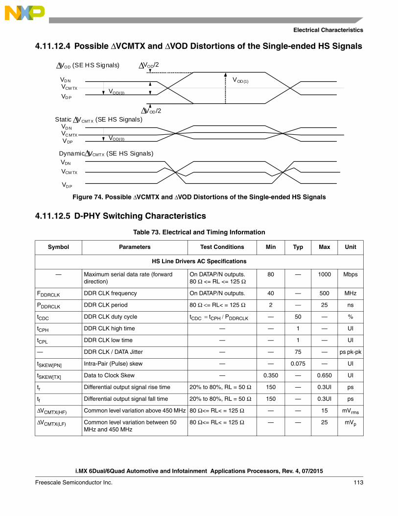
Electrical Characteristics
i.MX 6Dual/6Quad Automotive and Infotainment Applications Processors, Rev. 4, 07/2015
Freescale Semiconductor Inc. 113
4.11.12.4 Possible ΔVCMTX and ΔVOD Distortions of the Single-ended HS Signals
Figure 74. Possible ΔVCMTX and ΔVOD Distortions of the Single-ended HS Signals
4.11.12.5 D-PHY Switching Characteristics
Table 73. Electrical and Timing Information
Symbol Parameters Test Conditions Min Typ Max Unit
HS Line Drivers AC Specifications
— Maximum serial data rate (forward direction)
On DATAP/N outputs. 80 Ω <= RL <= 125 Ω
80 — 1000 Mbps
FDDRCLK DDR CLK frequency On DATAP/N outputs. 40 — 500 MHz
PDDRCLK DDR CLK period 80 Ω <= RL< = 125 Ω 2 — 25 ns
tCDC DDR CLK duty cycle tCDC = tCPH / PDDRCLK — 50 — %
tCPH DDR CLK high time — — 1 — UI
tCPL DDR CLK low time — — 1 — UI
— DDR CLK / DATA Jitter — — 75 — ps pk-pk
tSKEW[PN] Intra-Pair (Pulse) skew — — 0.075 — UI
tSKEW[TX] Data to Clock Skew — 0.350 — 0.650 UI
tr Differential output signal rise time 20% to 80%, RL = 50 Ω 150 — 0.3UI ps
tf Differential output signal fall time 20% to 80%, RL = 50 Ω 150 — 0.3UI ps
ΔVCMTX(HF) Common level variation above 450 MHz 80 Ω<= RL< = 125 Ω — — 15 mVrms
ΔVCMTX(LF) Common level variation between 50 MHz and 450 MHz
80 Ω<= RL< = 125 Ω — — 25 mVp
VOD(0)
VOD(1)
VOD/2
VOD/2
VOD (SE HS Signals)
Static VCMTX (SE HS Signals)
Dynamic VCMTX (SE HS Signals)
VDN
VCM TX
VD P
VD N
VC MTX
VDP
VDN
VCM TX
VD P
VOD(0)
ΔΔ
Δ
Δ
Δ
i.MX 6Dual/6Quad Automotive and Infotainment Applications Processors, Rev. 4, 07/2015
114 Freescale Semiconductor Inc.
Electrical Characteristics
LP Line Drivers AC Specifications
trlp,tflp Single ended output rise/fall time 15% to 85%, CL<70 pF — — 25 ns
treo — 30% to 85%, CL<70 pF — — 35 ns
δV/δtSR Signal slew rate 15% to 85%, CL<70 pF — — 120 mV/ns
CL Load capacitance — 0 — 70 pF
HS Line Receiver AC Specifications
tSETUP[RX] Data to Clock Receiver Setup time — 0.15 — — UI
tHOLD[RX] Clock to Data Receiver Hold time — 0.15 — — UI
ΔVCMRX(HF) Common mode interference beyond 450 MHz
— — — 200 mVpp
ΔVCMRX(LF) Common mode interference between 50 MHz and 450 MHz
— -50 — 50 mVpp
CCM Common mode termination — — — 60 pF
LP Line Receiver AC Specifications
eSPIKE Input pulse rejection — — — 300 Vps
TMIN Minimum pulse response — 50 — — ns
VINT Pk-to-Pk interference voltage — — — 400 mV
fINT Interference frequency — 450 — — MHz
Model Parameters used for Driver Load switching performance evaluation
CPAD Equivalent Single ended I/O PAD capacitance.
— — — 1 pF
CPIN Equivalent Single ended Package + PCB capacitance.
— — — 2 pF
LS Equivalent wire bond series inductance — — — 1.5 nH
RS Equivalent wire bond series resistance — — — 0.15 Ω
RL Load Resistance — 80 100 125 Ω
Table 73. Electrical and Timing Information (continued)
Symbol Parameters Test Conditions Min Typ Max Unit
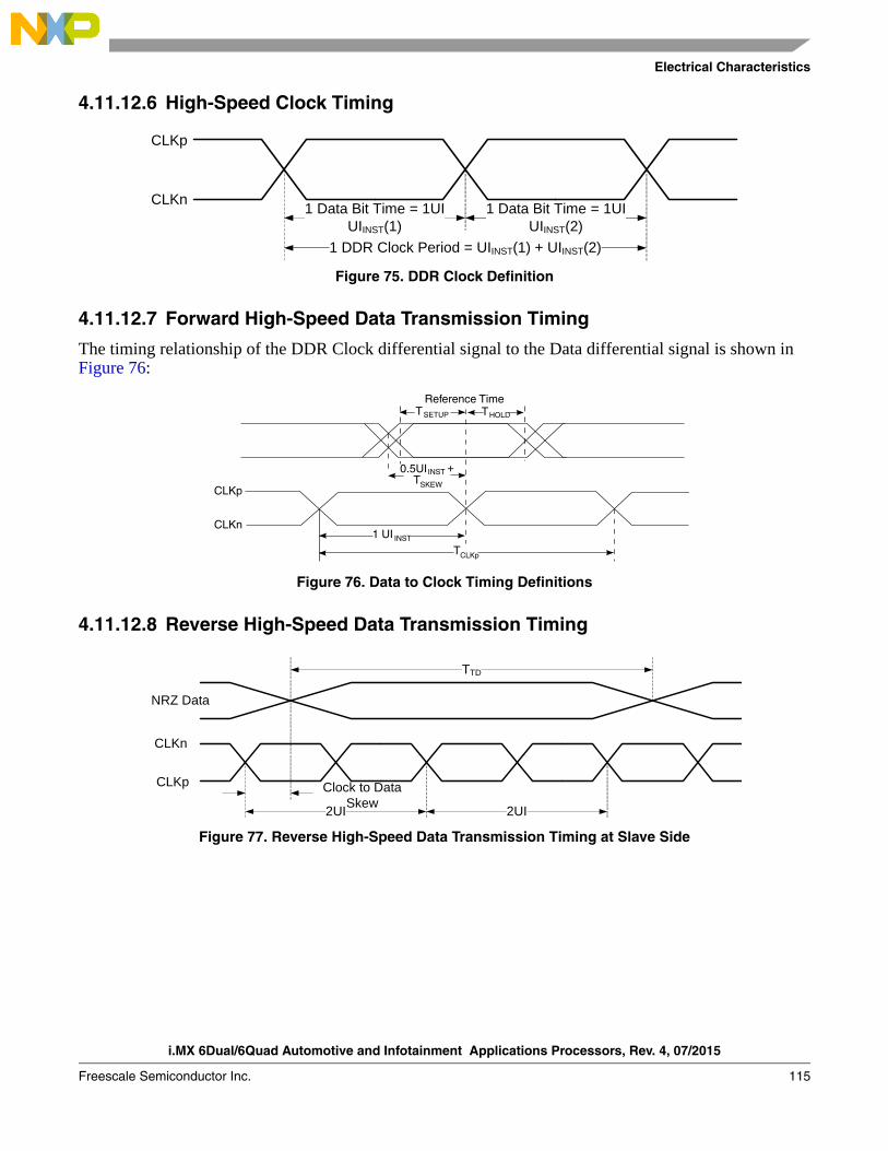
Electrical Characteristics
i.MX 6Dual/6Quad Automotive and Infotainment Applications Processors, Rev. 4, 07/2015
Freescale Semiconductor Inc. 115
4.11.12.6 High-Speed Clock Timing
Figure 75. DDR Clock Definition
4.11.12.7 Forward High-Speed Data Transmission Timing
The timing relationship of the DDR Clock differential signal to the Data differential signal is shown in Figure 76:
Figure 76. Data to Clock Timing Definitions
4.11.12.8 Reverse High-Speed Data Transmission Timing
Figure 77. Reverse High-Speed Data Transmission Timing at Slave Side
1 Data Bit Time = 1UIUIINST(1)
1 Data Bit Time = 1UIUIINST(2)
CLKp
CLKn
1 DDR Clock Period = UIINST(1) + UIINST(2)
TTD
2UI 2UI
CLKp
CLKn
Clock to Data Skew
NRZ Data
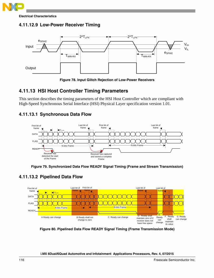
i.MX 6Dual/6Quad Automotive and Infotainment Applications Processors, Rev. 4, 07/2015
116 Freescale Semiconductor Inc.
Electrical Characteristics
4.11.12.9 Low-Power Receiver Timing
Figure 78. Input Glitch Rejection of Low-Power Receivers
4.11.13 HSI Host Controller Timing Parameters
This section describes the timing parameters of the HSI Host Controller which are compliant with High-Speed Synchronous Serial Interface (HSI) Physical Layer specification version 1.01.
4.11.13.1 Synchronous Data Flow
Figure 79. Synchronized Data Flow READY Signal Timing (Frame and Stream Transmission)
4.11.13.2 Pipelined Data Flow
Figure 80. Pipelined Data Flow READY Signal Timing (Frame Transmission Mode)
2*TLPX 2*TLPX
TMIN-RX TMIN-RX
eSPIKE
eSPIKE
Input
Output
VIH
VIL
N-bits Frame N-bits Frame
First bit of frame
tNomBit
Last bit of frame
First bit of frame
Last bit of frame
DATA
FLAG
READY
Receiver has detected the start
of the Frame
Receiver has captured and stored a complete
Frame
N-bits Frame
Last bit of frame
DATA
FLAG
N-bits Frame
First bit of frame
tNomBit
Last bit of frame
First bit of frame
READY
A Ready can change B Ready shall not change to zero
Last bit of frame
C. Ready can changeD. Ready shall
maintain zero of if receiver does not have free space
E. Ready
can change
F. Ready shall
maintain its value
G. Ready can change
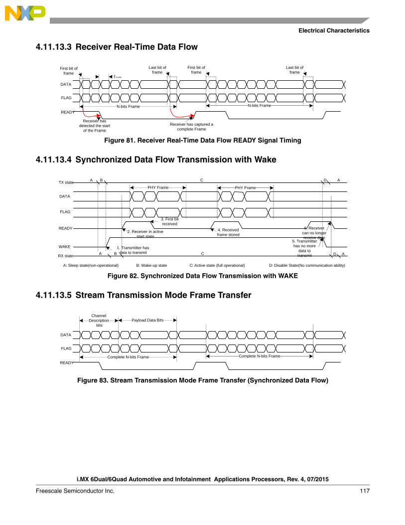
Electrical Characteristics
i.MX 6Dual/6Quad Automotive and Infotainment Applications Processors, Rev. 4, 07/2015
Freescale Semiconductor Inc. 117
4.11.13.3 Receiver Real-Time Data Flow
Figure 81. Receiver Real-Time Data Flow READY Signal Timing
4.11.13.4 Synchronized Data Flow Transmission with Wake
Figure 82. Synchronized Data Flow Transmission with WAKE
4.11.13.5 Stream Transmission Mode Frame Transfer
Figure 83. Stream Transmission Mode Frame Transfer (Synchronized Data Flow)
N-bits Frame N-bits Frame
First bit of frame
tNomBit
Last bit of frame
First bit of frame
Last bit of frame
DATA
FLAG
READY
Receiver has detected the start
of the Frame
Receiver has captured a complete Frame
DATA
FLAG
READY
1. Transmitter has data to transmit
3. First bit received
PHY Frame PHY FrameTX state
RX state
WAKE
A
A
B
B
C
C
D
D
A
A
2. Receiver in active start state
4. Received frame stored
5. Transmitter has no more
data to transmit
6. Receiver can no longer receive date
A: Sleep state(non-operational) B: Wake-up state C: Active state (full operational) D: Disable State(No communication ability)
Complete N-bits Frame Complete N-bits Frame
DATA
FLAG
READY
Channel Description
bitsPayload Data Bits
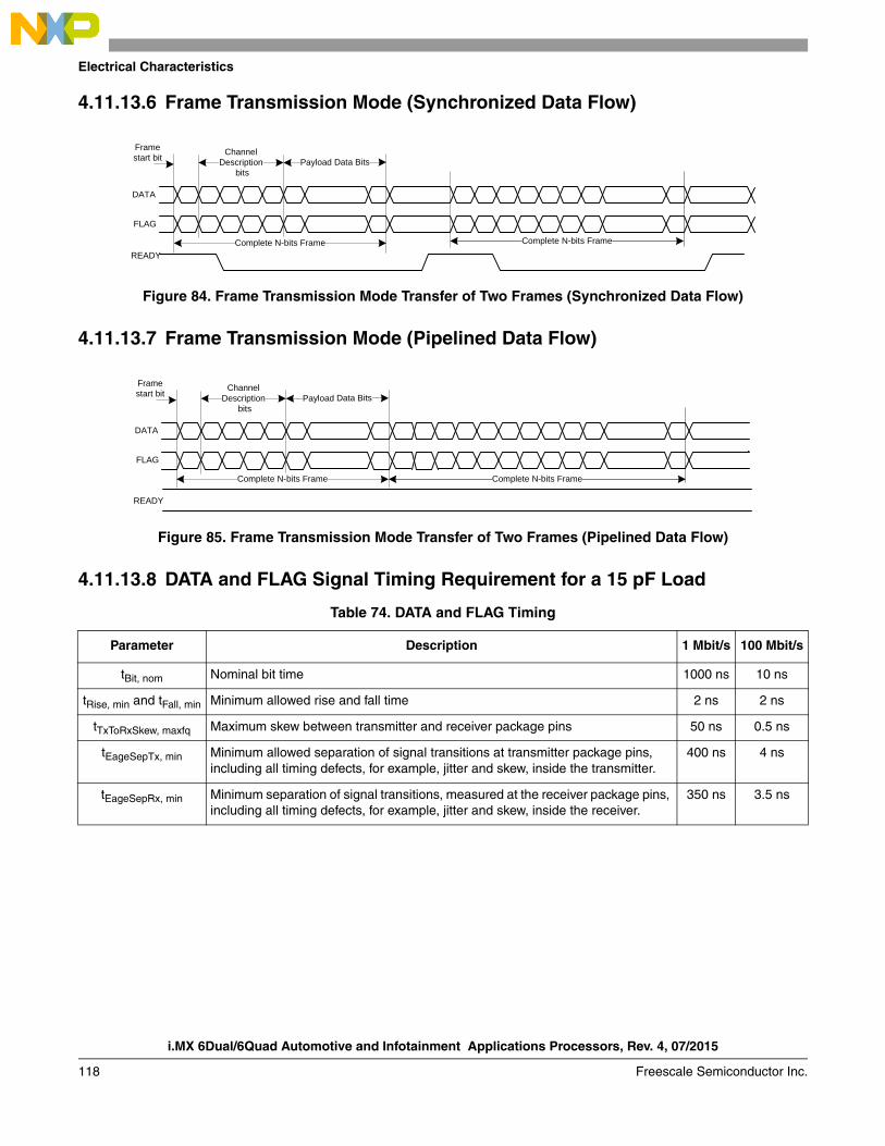
i.MX 6Dual/6Quad Automotive and Infotainment Applications Processors, Rev. 4, 07/2015
118 Freescale Semiconductor Inc.
Electrical Characteristics
4.11.13.6 Frame Transmission Mode (Synchronized Data Flow)
Figure 84. Frame Transmission Mode Transfer of Two Frames (Synchronized Data Flow)
4.11.13.7 Frame Transmission Mode (Pipelined Data Flow)
Figure 85. Frame Transmission Mode Transfer of Two Frames (Pipelined Data Flow)
4.11.13.8 DATA and FLAG Signal Timing Requirement for a 15 pF Load
Table 74. DATA and FLAG Timing
Parameter Description 1 Mbit/s 100 Mbit/s
tBit, nom Nominal bit time 1000 ns 10 ns
tRise, min and tFall, min Minimum allowed rise and fall time 2 ns 2 ns
tTxToRxSkew, maxfq Maximum skew between transmitter and receiver package pins 50 ns 0.5 ns
tEageSepTx, min Minimum allowed separation of signal transitions at transmitter package pins, including all timing defects, for example, jitter and skew, inside the transmitter.
400 ns 4 ns
tEageSepRx, min Minimum separation of signal transitions, measured at the receiver package pins, including all timing defects, for example, jitter and skew, inside the receiver.
350 ns 3.5 ns
Complete N-bits Frame Complete N-bits Frame
DATA
FLAG
READY
Channel Description
bitsPayload Data Bits
Frame start bit
Complete N-bits Frame Complete N-bits Frame
DATA
FLAG
READY
Channel Description
bitsPayload Data Bits
Frame start bit
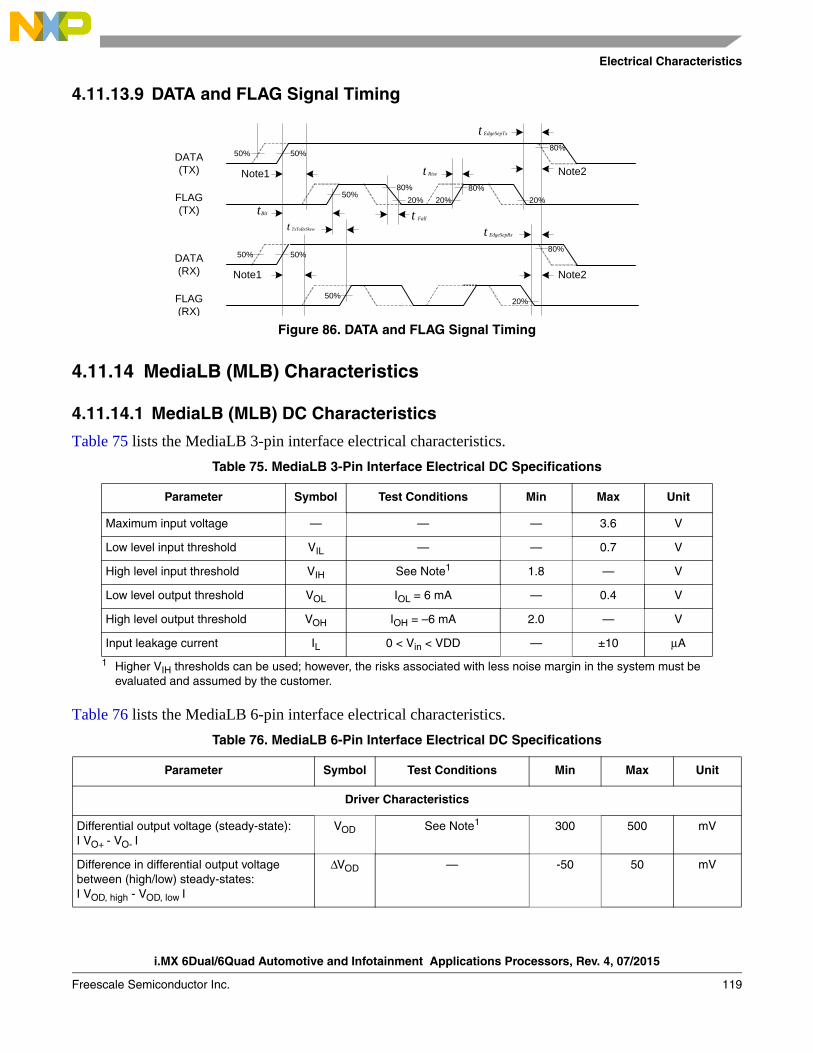
Electrical Characteristics
i.MX 6Dual/6Quad Automotive and Infotainment Applications Processors, Rev. 4, 07/2015
Freescale Semiconductor Inc. 119
4.11.13.9 DATA and FLAG Signal Timing
Figure 86. DATA and FLAG Signal Timing
4.11.14 MediaLB (MLB) Characteristics
4.11.14.1 MediaLB (MLB) DC Characteristics
Table 75 lists the MediaLB 3-pin interface electrical characteristics.
Table 76 lists the MediaLB 6-pin interface electrical characteristics.
Table 75. MediaLB 3-Pin Interface Electrical DC Specifications
Parameter Symbol Test Conditions Min Max Unit
Maximum input voltage — — — 3.6 V
Low level input threshold VIL — — 0.7 V
High level input threshold VIH See Note1
1 Higher VIH thresholds can be used; however, the risks associated with less noise margin in the system must be evaluated and assumed by the customer.
1.8 — V
Low level output threshold VOL IOL = 6 mA — 0.4 V
High level output threshold VOH IOH = –6 mA 2.0 — V
Input leakage current IL 0 < Vin < VDD — ±10 μA
Table 76. MediaLB 6-Pin Interface Electrical DC Specifications
Parameter Symbol Test Conditions Min Max Unit
Driver Characteristics
Differential output voltage (steady-state):I VO+ - VO- I
VOD See Note1 300 500 mV
Difference in differential output voltage between (high/low) steady-states:I VOD, high - VOD, low I
ΔVOD — -50 50 mV
DATA(TX)
FLAG(TX)
DATA(RX)
FLAG(RX)
50%
50%50%
50%
50%
50%
80%80%
20%
20%20%20%
80%
80%
t EdgeSepTx
t TxToRxSkew t EdgeSepRx
tBit
t Rise
t Fall
Note1
Note1 Note2
Note2
i.MX 6Dual/6Quad Automotive and Infotainment Applications Processors, Rev. 4, 07/2015
120 Freescale Semiconductor Inc.
Electrical Characteristics
Common-mode output voltage:(VO+ - VO-) / 2
VOCM — 1.0 1.5 V
Difference in common-mode output between (high/low) steady-states:I VOCM, high - VOCM, low I
ΔVOCM — -50 50 mV
Variations on common-mode output during a logic state transitions
VCMV See Note2 — 150 mVpp
Short circuit current |IOS| See Note3 — 43 mA
Differential output impedance ZO — 1.6 — kΩ
Receiver Characteristics
Differential clock input: • logic low steady-state • logic high steady-state • hysteresis
VILCVIHCVHSC
See Note4
50-25
-50
25
mVmVmV
Differential signal/data input: • logic low steady-state • logic high steady-state
VILSVIHS
——50
-50—
mVmV
Signal-ended input voltage (steady-state): • MLB_SIG_P, MLB_DATA_P • MLB_SIG_N, MLB_DATA_N VIN+
VIN-
—
0.50.5
2.02.0
VV
1 The signal-ended output voltage of a driver is defined as VO+ on MLB_CLK_P, MLB_SIG_P, and MLB_DATA_P. The signal-ended output voltage of a driver is defined as VO- on MLB_CLK_N, MLB_SIG_N, and MLB_DATA_N.
2 Variations in the common-mode voltage can occur between logic states (for example, during state transitions) as a result of differences in the transition rate of VO+ and VO-.
3 Short circuit current is applicable when VO+ and VO- are shorted together and/or shorted to ground.4 The logic state of the receiver is undefined when -50 mV < VID < 50 mV.
Table 76. MediaLB 6-Pin Interface Electrical DC Specifications (continued)
Parameter Symbol Test Conditions Min Max Unit
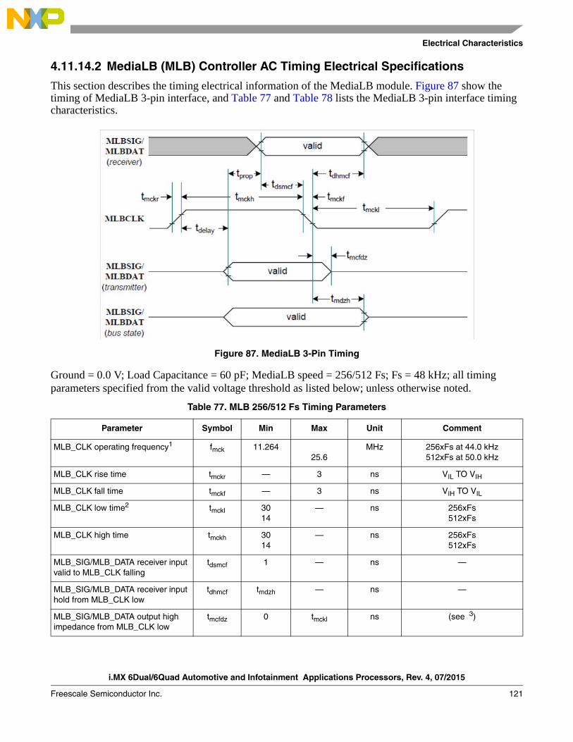
Electrical Characteristics
i.MX 6Dual/6Quad Automotive and Infotainment Applications Processors, Rev. 4, 07/2015
Freescale Semiconductor Inc. 121
4.11.14.2 MediaLB (MLB) Controller AC Timing Electrical Specifications
This section describes the timing electrical information of the MediaLB module. Figure 87 show the timing of MediaLB 3-pin interface, and Table 77 and Table 78 lists the MediaLB 3-pin interface timing characteristics.
Figure 87. MediaLB 3-Pin Timing
Ground = 0.0 V; Load Capacitance = 60 pF; MediaLB speed = 256/512 Fs; Fs = 48 kHz; all timing parameters specified from the valid voltage threshold as listed below; unless otherwise noted.
Table 77. MLB 256/512 Fs Timing Parameters
Parameter Symbol Min Max Unit Comment
MLB_CLK operating frequency1 fmck 11.26425.6
MHz 256xFs at 44.0 kHz512xFs at 50.0 kHz
MLB_CLK rise time tmckr — 3 ns VIL TO VIH
MLB_CLK fall time tmckf — 3 ns VIH TO VIL
MLB_CLK low time2 tmckl 3014
— ns 256xFs512xFs
MLB_CLK high time tmckh 3014
— ns 256xFs512xFs
MLB_SIG/MLB_DATA receiver input valid to MLB_CLK falling
tdsmcf 1 — ns —
MLB_SIG/MLB_DATA receiver input hold from MLB_CLK low
tdhmcf tmdzh — ns —
MLB_SIG/MLB_DATA output high impedance from MLB_CLK low
tmcfdz 0 tmckl ns (see 3)
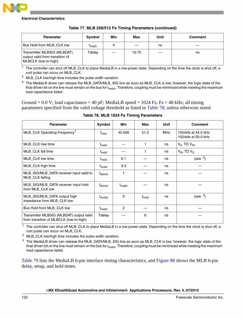
i.MX 6Dual/6Quad Automotive and Infotainment Applications Processors, Rev. 4, 07/2015
122 Freescale Semiconductor Inc.
Electrical Characteristics
Ground = 0.0 V; load capacitance = 40 pF; MediaLB speed = 1024 Fs; Fs = 48 kHz; all timing parameters specified from the valid voltage threshold as listed in Table 78; unless otherwise noted.
Table 79 lists the MediaLB 6-pin interface timing characteristics, and Figure 88 shows the MLB 6-pin delay, setup, and hold times.
Bus Hold from MLB_CLK low tmdzh 4 — ns —
Transmitter MLBSIG (MLBDAT) output valid from transition of MLBCLK (low-to-high)
Tdelay — 10.75 — ns
1 The controller can shut off MLB_CLK to place MediaLB in a low-power state. Depending on the time the clock is shut off, a runt pulse can occur on MLB_CLK.
2 MLB_CLK low/high time includes the pulse width variation.3 The MediaLB driver can release the MLB_DATA/MLB_SIG line as soon as MLB_CLK is low; however, the logic state of the
final driven bit on the line must remain on the bus for tmdzh. Therefore, coupling must be minimized while meeting the maximum load capacitance listed.
Table 78. MLB 1024 Fs Timing Parameters
Parameter Symbol Min Max Unit Comment
MLB_CLK Operating Frequency1
1 The controller can shut off MLB_CLK to place MediaLB in a low-power state. Depending on the time the clock is shut off, a runt pulse can occur on MLB_CLK.
fmck 45.056 51.2 MHz 1024xfs at 44.0 kHz1024xfs at 50.0 kHz
MLB_CLK rise time tmckr — 1 ns VIL TO VIH
MLB_CLK fall time tmckf — 1 ns VIH TO VIL
MLB_CLK low time tmckl 6.1 — ns (see 2)
2 MLB_CLK low/high time includes the pulse width variation.
MLB_CLK high time tmckh 9.3 — ns —
MLB_SIG/MLB_DATA receiver input valid to MLB_CLK falling
tdsmcf 1 — ns —
MLB_SIG/MLB_DATA receiver input hold from MLB_CLK low
tdhmcf tmdzh — ns —
MLB_SIG/MLB_DATA output high impedance from MLB_CLK low
tmcfdz 0 tmckl ns (see 3)
3 The MediaLB driver can release the MLB_DATA/MLB_SIG line as soon as MLB_CLK is low; however, the logic state of the final driven bit on the line must remain on the bus for tmdzh. Therefore, coupling must be minimized while meeting the maximum load capacitance listed.
Bus Hold from MLB_CLK low tmdzh 2 — ns —
Transmitter MLBSIG (MLBDAT) output valid from transition of MLBCLK (low-to-high)
Tdelay — 6 ns —
Table 77. MLB 256/512 Fs Timing Parameters (continued)
Parameter Symbol Min Max Unit Comment
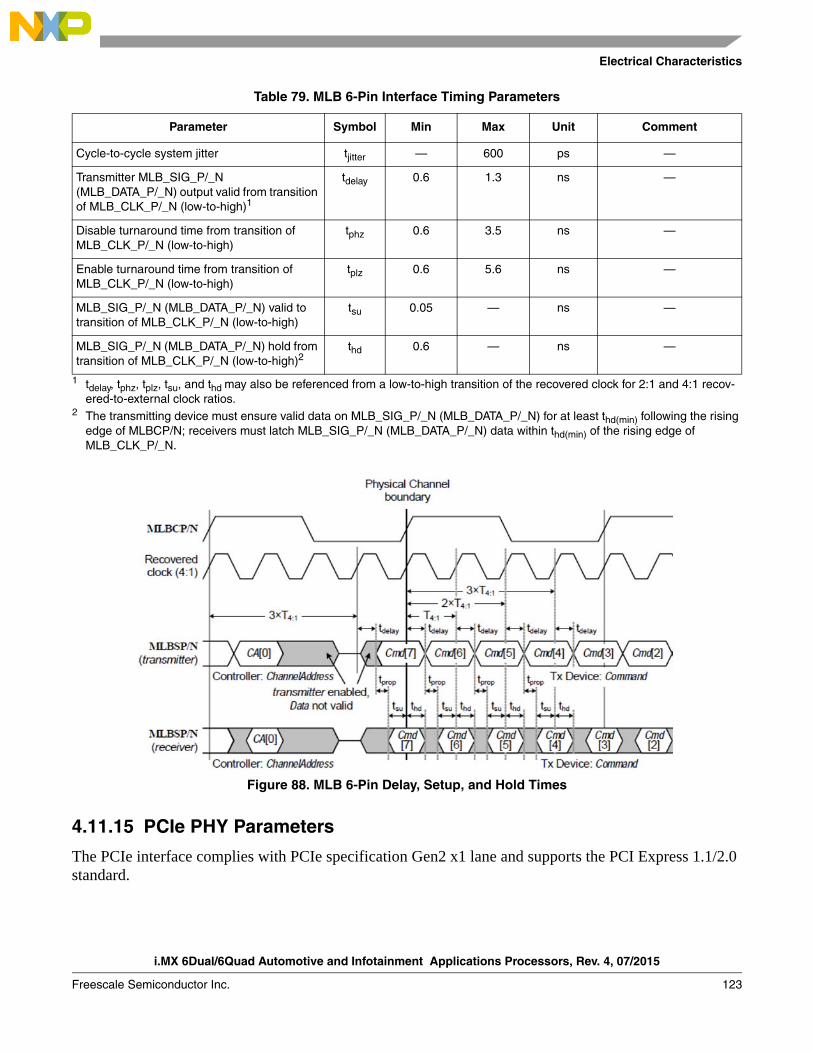
Electrical Characteristics
i.MX 6Dual/6Quad Automotive and Infotainment Applications Processors, Rev. 4, 07/2015
Freescale Semiconductor Inc. 123
Figure 88. MLB 6-Pin Delay, Setup, and Hold Times
4.11.15 PCIe PHY Parameters
The PCIe interface complies with PCIe specification Gen2 x1 lane and supports the PCI Express 1.1/2.0 standard.
Table 79. MLB 6-Pin Interface Timing Parameters
Parameter Symbol Min Max Unit Comment
Cycle-to-cycle system jitter tjitter — 600 ps —
Transmitter MLB_SIG_P/_N (MLB_DATA_P/_N) output valid from transition of MLB_CLK_P/_N (low-to-high)1
1 tdelay, tphz, tplz, tsu, and thd may also be referenced from a low-to-high transition of the recovered clock for 2:1 and 4:1 recov-ered-to-external clock ratios.
tdelay 0.6 1.3 ns —
Disable turnaround time from transition of MLB_CLK_P/_N (low-to-high)
tphz 0.6 3.5 ns —
Enable turnaround time from transition of MLB_CLK_P/_N (low-to-high)
tplz 0.6 5.6 ns —
MLB_SIG_P/_N (MLB_DATA_P/_N) valid to transition of MLB_CLK_P/_N (low-to-high)
tsu 0.05 — ns —
MLB_SIG_P/_N (MLB_DATA_P/_N) hold from transition of MLB_CLK_P/_N (low-to-high)2
2 The transmitting device must ensure valid data on MLB_SIG_P/_N (MLB_DATA_P/_N) for at least thd(min) following the rising edge of MLBCP/N; receivers must latch MLB_SIG_P/_N (MLB_DATA_P/_N) data within thd(min) of the rising edge of MLB_CLK_P/_N.
thd 0.6 — ns —
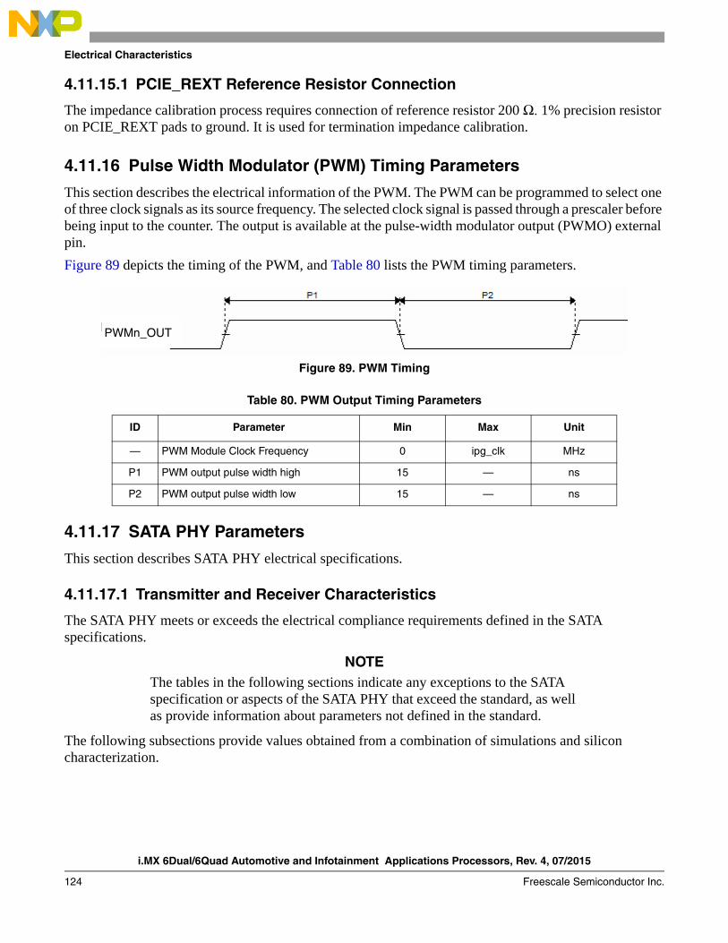
i.MX 6Dual/6Quad Automotive and Infotainment Applications Processors, Rev. 4, 07/2015
124 Freescale Semiconductor Inc.
Electrical Characteristics
4.11.15.1 PCIE_REXT Reference Resistor Connection
The impedance calibration process requires connection of reference resistor 200 Ω. 1% precision resistor on PCIE_REXT pads to ground. It is used for termination impedance calibration.
4.11.16 Pulse Width Modulator (PWM) Timing Parameters
This section describes the electrical information of the PWM. The PWM can be programmed to select one of three clock signals as its source frequency. The selected clock signal is passed through a prescaler before being input to the counter. The output is available at the pulse-width modulator output (PWMO) external pin.
Figure 89 depicts the timing of the PWM, and Table 80 lists the PWM timing parameters.
Figure 89. PWM Timing
4.11.17 SATA PHY Parameters
This section describes SATA PHY electrical specifications.
4.11.17.1 Transmitter and Receiver Characteristics
The SATA PHY meets or exceeds the electrical compliance requirements defined in the SATA specifications.
NOTEThe tables in the following sections indicate any exceptions to the SATA specification or aspects of the SATA PHY that exceed the standard, as well as provide information about parameters not defined in the standard.
The following subsections provide values obtained from a combination of simulations and silicon characterization.
Table 80. PWM Output Timing Parameters
ID Parameter Min Max Unit
— PWM Module Clock Frequency 0 ipg_clk MHz
P1 PWM output pulse width high 15 — ns
P2 PWM output pulse width low 15 — ns
PWMn_OUT
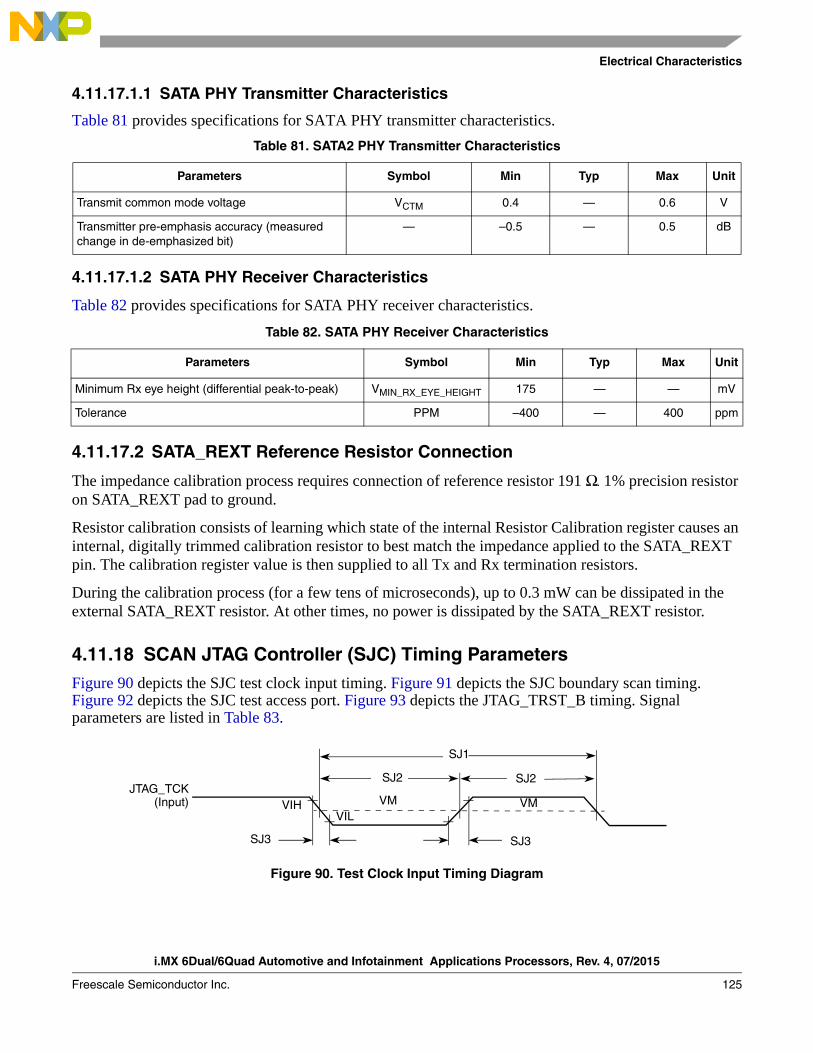
Electrical Characteristics
i.MX 6Dual/6Quad Automotive and Infotainment Applications Processors, Rev. 4, 07/2015
Freescale Semiconductor Inc. 125
4.11.17.1.1 SATA PHY Transmitter Characteristics
Table 81 provides specifications for SATA PHY transmitter characteristics.
4.11.17.1.2 SATA PHY Receiver Characteristics
Table 82 provides specifications for SATA PHY receiver characteristics.
4.11.17.2 SATA_REXT Reference Resistor Connection
The impedance calibration process requires connection of reference resistor 191 Ω. 1% precision resistor on SATA_REXT pad to ground.
Resistor calibration consists of learning which state of the internal Resistor Calibration register causes an internal, digitally trimmed calibration resistor to best match the impedance applied to the SATA_REXT pin. The calibration register value is then supplied to all Tx and Rx termination resistors.
During the calibration process (for a few tens of microseconds), up to 0.3 mW can be dissipated in the external SATA_REXT resistor. At other times, no power is dissipated by the SATA_REXT resistor.
4.11.18 SCAN JTAG Controller (SJC) Timing ParametersFigure 90 depicts the SJC test clock input timing. Figure 91 depicts the SJC boundary scan timing. Figure 92 depicts the SJC test access port. Figure 93 depicts the JTAG_TRST_B timing. Signal parameters are listed in Table 83.
Figure 90. Test Clock Input Timing Diagram
Table 81. SATA2 PHY Transmitter Characteristics
Parameters Symbol Min Typ Max Unit
Transmit common mode voltage VCTM 0.4 — 0.6 V
Transmitter pre-emphasis accuracy (measured change in de-emphasized bit)
— –0.5 — 0.5 dB
Table 82. SATA PHY Receiver Characteristics
Parameters Symbol Min Typ Max Unit
Minimum Rx eye height (differential peak-to-peak) VMIN_RX_EYE_HEIGHT 175 — — mV
Tolerance PPM –400 — 400 ppm
JTAG_TCK(Input) VM VMVIH
VIL
SJ1
SJ2 SJ2
SJ3SJ3
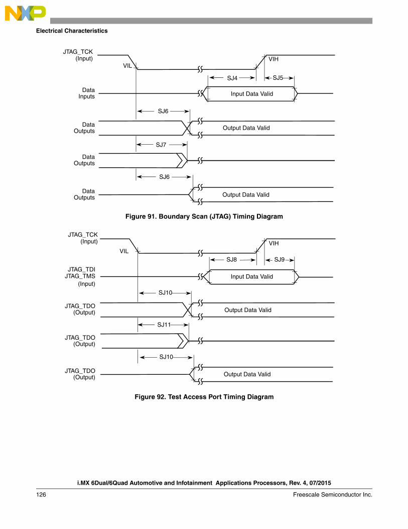
i.MX 6Dual/6Quad Automotive and Infotainment Applications Processors, Rev. 4, 07/2015
126 Freescale Semiconductor Inc.
Electrical Characteristics
Figure 91. Boundary Scan (JTAG) Timing Diagram
Figure 92. Test Access Port Timing Diagram
JTAG_TCK(Input)
DataInputs
DataOutputs
DataOutputs
DataOutputs
VIHVIL
Input Data Valid
Output Data Valid
Output Data Valid
SJ4 SJ5
SJ6
SJ7
SJ6
JTAG_TCK(Input)
JTAG_TDI
(Input)
JTAG_TDO(Output)
JTAG_TDO(Output)
JTAG_TDO(Output)
VIHVIL
Input Data Valid
Output Data Valid
Output Data Valid
JTAG_TMS
SJ8 SJ9
SJ10
SJ11
SJ10
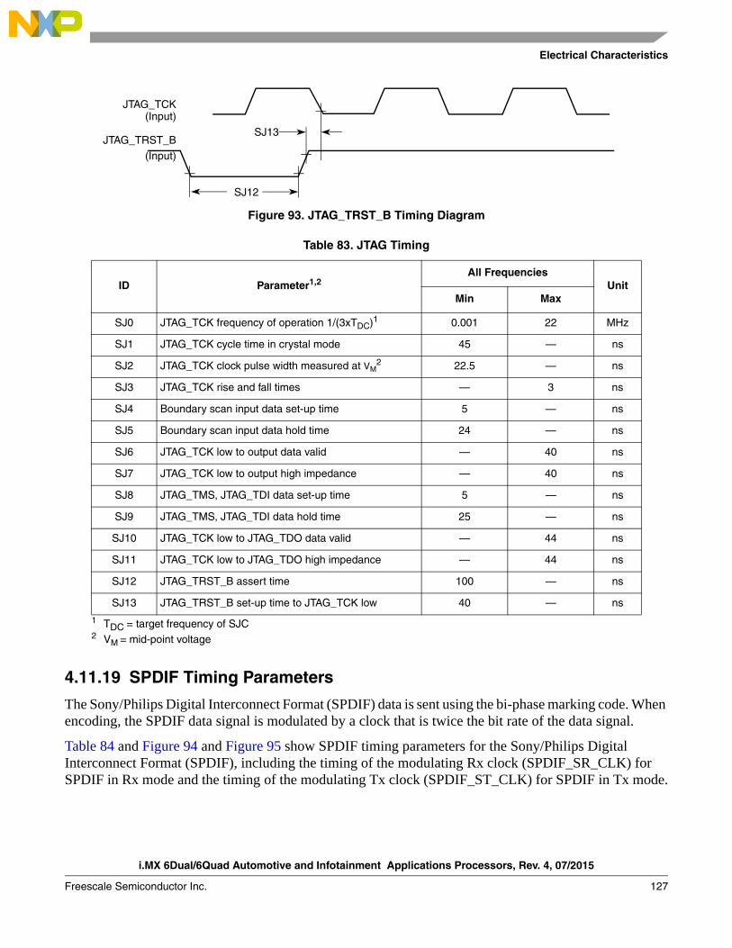
Electrical Characteristics
i.MX 6Dual/6Quad Automotive and Infotainment Applications Processors, Rev. 4, 07/2015
Freescale Semiconductor Inc. 127
Figure 93. JTAG_TRST_B Timing Diagram
4.11.19 SPDIF Timing Parameters
The Sony/Philips Digital Interconnect Format (SPDIF) data is sent using the bi-phase marking code. When encoding, the SPDIF data signal is modulated by a clock that is twice the bit rate of the data signal.
Table 84 and Figure 94 and Figure 95 show SPDIF timing parameters for the Sony/Philips Digital Interconnect Format (SPDIF), including the timing of the modulating Rx clock (SPDIF_SR_CLK) for SPDIF in Rx mode and the timing of the modulating Tx clock (SPDIF_ST_CLK) for SPDIF in Tx mode.
Table 83. JTAG Timing
ID Parameter1,2All Frequencies
Unit Min Max
SJ0 JTAG_TCK frequency of operation 1/(3xTDC)1
1 TDC = target frequency of SJC
0.001 22 MHz
SJ1 JTAG_TCK cycle time in crystal mode 45 — ns
SJ2 JTAG_TCK clock pulse width measured at VM2
2 VM = mid-point voltage
22.5 — ns
SJ3 JTAG_TCK rise and fall times — 3 ns
SJ4 Boundary scan input data set-up time 5 — ns
SJ5 Boundary scan input data hold time 24 — ns
SJ6 JTAG_TCK low to output data valid — 40 ns
SJ7 JTAG_TCK low to output high impedance — 40 ns
SJ8 JTAG_TMS, JTAG_TDI data set-up time 5 — ns
SJ9 JTAG_TMS, JTAG_TDI data hold time 25 — ns
SJ10 JTAG_TCK low to JTAG_TDO data valid — 44 ns
SJ11 JTAG_TCK low to JTAG_TDO high impedance — 44 ns
SJ12 JTAG_TRST_B assert time 100 — ns
SJ13 JTAG_TRST_B set-up time to JTAG_TCK low 40 — ns
JTAG_TCK(Input)
(Input)
SJ13
SJ12
JTAG_TRST_B
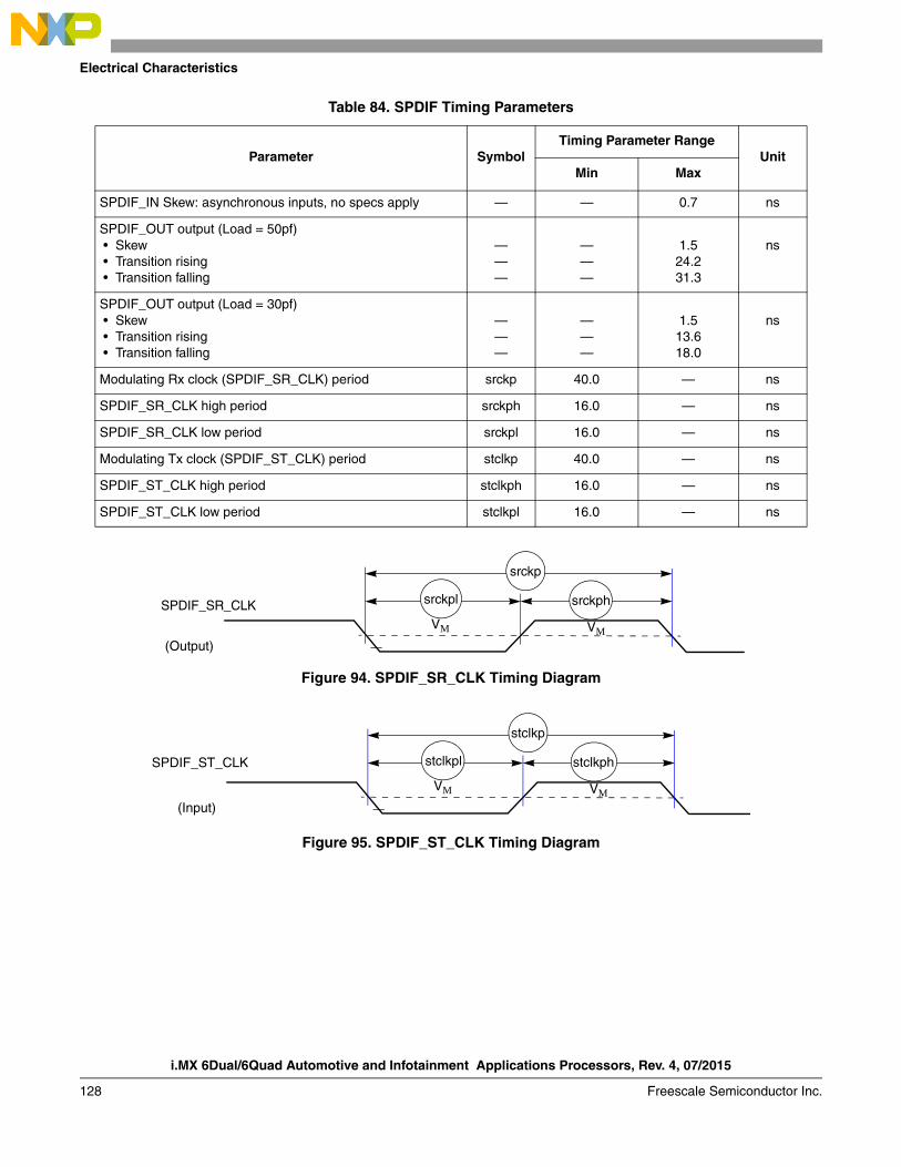
i.MX 6Dual/6Quad Automotive and Infotainment Applications Processors, Rev. 4, 07/2015
128 Freescale Semiconductor Inc.
Electrical Characteristics
Figure 94. SPDIF_SR_CLK Timing Diagram
Figure 95. SPDIF_ST_CLK Timing Diagram
Table 84. SPDIF Timing Parameters
Parameter SymbolTiming Parameter Range
Unit Min Max
SPDIF_IN Skew: asynchronous inputs, no specs apply — — 0.7 ns
SPDIF_OUT output (Load = 50pf) • Skew • Transition rising • Transition falling
———
———
1.524.231.3
ns
SPDIF_OUT output (Load = 30pf) • Skew • Transition rising • Transition falling
———
———
1.513.618.0
ns
Modulating Rx clock (SPDIF_SR_CLK) period srckp 40.0 — ns
SPDIF_SR_CLK high period srckph 16.0 — ns
SPDIF_SR_CLK low period srckpl 16.0 — ns
Modulating Tx clock (SPDIF_ST_CLK) period stclkp 40.0 — ns
SPDIF_ST_CLK high period stclkph 16.0 — ns
SPDIF_ST_CLK low period stclkpl 16.0 — ns
SPDIF_SR_CLK
(Output)
VM VM
srckp
srckphsrckpl
SPDIF_ST_CLK
(Input)
VM VM
stclkp
stclkphstclkpl
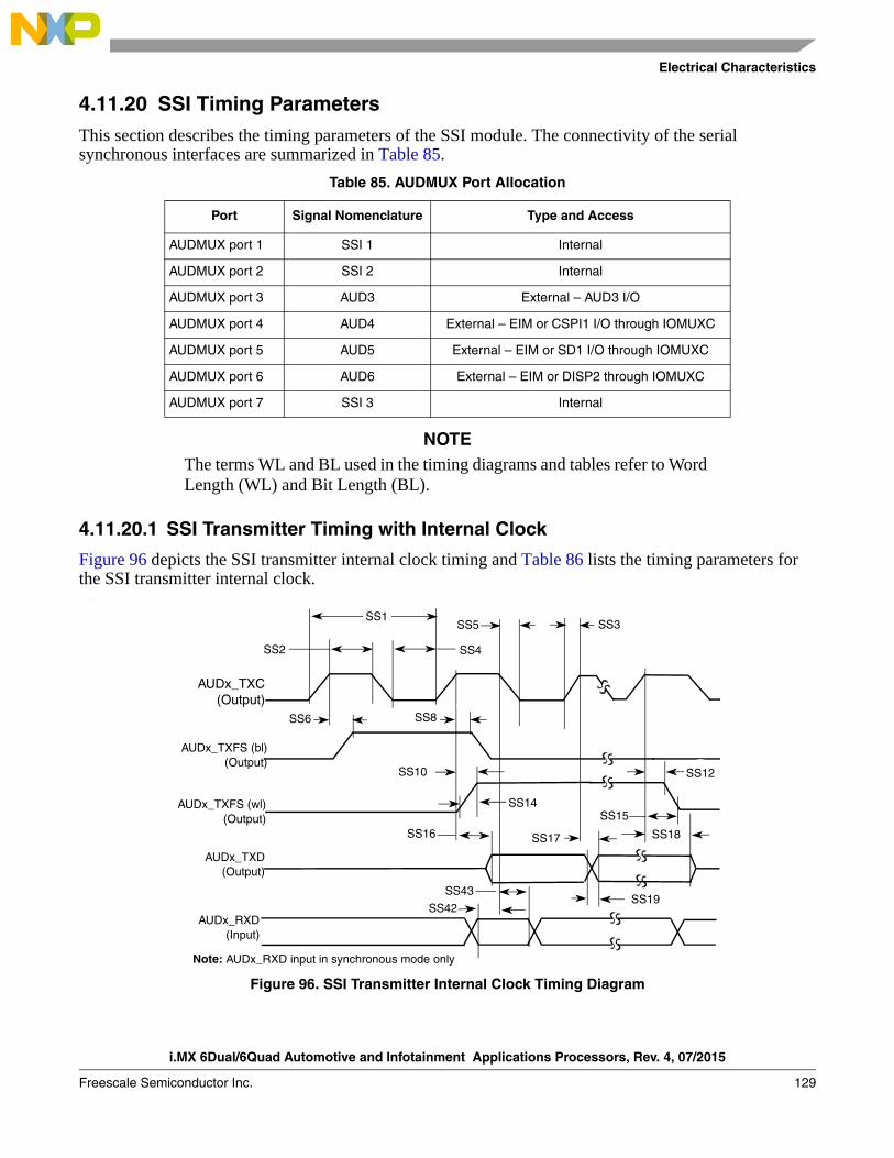
Electrical Characteristics
i.MX 6Dual/6Quad Automotive and Infotainment Applications Processors, Rev. 4, 07/2015
Freescale Semiconductor Inc. 129
4.11.20 SSI Timing ParametersThis section describes the timing parameters of the SSI module. The connectivity of the serial synchronous interfaces are summarized in Table 85.
NOTEThe terms WL and BL used in the timing diagrams and tables refer to Word Length (WL) and Bit Length (BL).
4.11.20.1 SSI Transmitter Timing with Internal Clock
Figure 96 depicts the SSI transmitter internal clock timing and Table 86 lists the timing parameters for the SSI transmitter internal clock.
.
Figure 96. SSI Transmitter Internal Clock Timing Diagram
Table 85. AUDMUX Port Allocation
Port Signal Nomenclature Type and Access
AUDMUX port 1 SSI 1 Internal
AUDMUX port 2 SSI 2 Internal
AUDMUX port 3 AUD3 External – AUD3 I/O
AUDMUX port 4 AUD4 External – EIM or CSPI1 I/O through IOMUXC
AUDMUX port 5 AUD5 External – EIM or SD1 I/O through IOMUXC
AUDMUX port 6 AUD6 External – EIM or DISP2 through IOMUXC
AUDMUX port 7 SSI 3 Internal
SS19
SS1
SS2 SS4
SS3SS5
SS6 SS8
SS10 SS12
SS14
SS18
SS15
SS17SS16
SS43
SS42
Note: AUDx_RXD input in synchronous mode only
AUDx_TXC(Output)
AUDx_TXFS (wl)(Output)
AUDx_TXFS (bl)(Output)
AUDx_RXD(Input)
AUDx_TXD(Output)
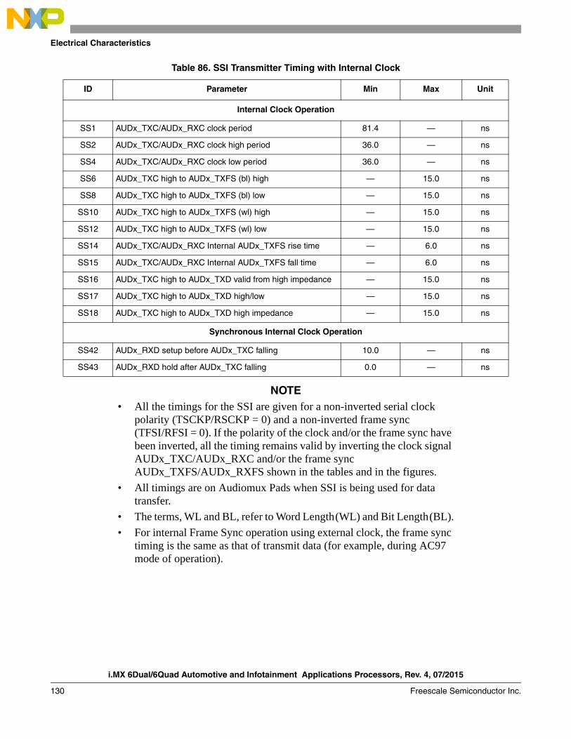
i.MX 6Dual/6Quad Automotive and Infotainment Applications Processors, Rev. 4, 07/2015
130 Freescale Semiconductor Inc.
Electrical Characteristics
NOTE• All the timings for the SSI are given for a non-inverted serial clock
polarity (TSCKP/RSCKP = 0) and a non-inverted frame sync (TFSI/RFSI = 0). If the polarity of the clock and/or the frame sync have been inverted, all the timing remains valid by inverting the clock signal AUDx_TXC/AUDx_RXC and/or the frame sync AUDx_TXFS/AUDx_RXFS shown in the tables and in the figures.
• All timings are on Audiomux Pads when SSI is being used for data transfer.
• The terms, WL and BL, refer to Word Length(WL) and Bit Length(BL).
• For internal Frame Sync operation using external clock, the frame sync timing is the same as that of transmit data (for example, during AC97 mode of operation).
Table 86. SSI Transmitter Timing with Internal Clock
ID Parameter Min Max Unit
Internal Clock Operation
SS1 AUDx_TXC/AUDx_RXC clock period 81.4 — ns
SS2 AUDx_TXC/AUDx_RXC clock high period 36.0 — ns
SS4 AUDx_TXC/AUDx_RXC clock low period 36.0 — ns
SS6 AUDx_TXC high to AUDx_TXFS (bl) high — 15.0 ns
SS8 AUDx_TXC high to AUDx_TXFS (bl) low — 15.0 ns
SS10 AUDx_TXC high to AUDx_TXFS (wl) high — 15.0 ns
SS12 AUDx_TXC high to AUDx_TXFS (wl) low — 15.0 ns
SS14 AUDx_TXC/AUDx_RXC Internal AUDx_TXFS rise time — 6.0 ns
SS15 AUDx_TXC/AUDx_RXC Internal AUDx_TXFS fall time — 6.0 ns
SS16 AUDx_TXC high to AUDx_TXD valid from high impedance — 15.0 ns
SS17 AUDx_TXC high to AUDx_TXD high/low — 15.0 ns
SS18 AUDx_TXC high to AUDx_TXD high impedance — 15.0 ns
Synchronous Internal Clock Operation
SS42 AUDx_RXD setup before AUDx_TXC falling 10.0 — ns
SS43 AUDx_RXD hold after AUDx_TXC falling 0.0 — ns
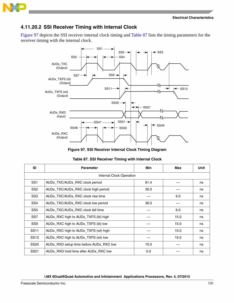
Electrical Characteristics
i.MX 6Dual/6Quad Automotive and Infotainment Applications Processors, Rev. 4, 07/2015
Freescale Semiconductor Inc. 131
4.11.20.2 SSI Receiver Timing with Internal Clock
Figure 97 depicts the SSI receiver internal clock timing and Table 87 lists the timing parameters for the receiver timing with the internal clock.
Figure 97. SSI Receiver Internal Clock Timing Diagram
Table 87. SSI Receiver Timing with Internal Clock
ID Parameter Min Max Unit
Internal Clock Operation
SS1 AUDx_TXC/AUDx_RXC clock period 81.4 — ns
SS2 AUDx_TXC/AUDx_RXC clock high period 36.0 — ns
SS3 AUDx_TXC/AUDx_RXC clock rise time — 6.0 ns
SS4 AUDx_TXC/AUDx_RXC clock low period 36.0 — ns
SS5 AUDx_TXC/AUDx_RXC clock fall time — 6.0 ns
SS7 AUDx_RXC high to AUDx_TXFS (bl) high — 15.0 ns
SS9 AUDx_RXC high to AUDx_TXFS (bl) low — 15.0 ns
SS11 AUDx_RXC high to AUDx_TXFS (wl) high — 15.0 ns
SS13 AUDx_RXC high to AUDx_TXFS (wl) low — 15.0 ns
SS20 AUDx_RXD setup time before AUDx_RXC low 10.0 — ns
SS21 AUDx_RXD hold time after AUDx_RXC low 0.0 — ns
SS50SS48
SS1
SS4SS2
SS51
SS20
SS21
SS49
SS7 SS9
SS11 SS13
SS47
SS3SS5
AUDx_TXC(Output)
AUDx_TXFS (bl)(Output)
AUDx_TXFS (wl)(Output)
AUDx_RXD(Input)
AUDx_RXC(Output)
i.MX 6Dual/6Quad Automotive and Infotainment Applications Processors, Rev. 4, 07/2015
132 Freescale Semiconductor Inc.
Electrical Characteristics
NOTE• All the timings for the SSI are given for a non-inverted serial clock
polarity (TSCKP/RSCKP = 0) and a non-inverted frame sync (TFSI/RFSI = 0). If the polarity of the clock and/or the frame sync have been inverted, all the timing remains valid by inverting the clock signal AUDx_TXC/AUDx_RXC and/or the frame sync AUDx_TXFS/AUDx_RXFS shown in the tables and in the figures.
• All timings are on Audiomux Pads when SSI is being used for data transfer.
• AUDx_TXC and AUDx_RXC refer to the Transmit and Receive sections of the SSI.
• The terms, WL and BL, refer to Word Length (WL) and Bit Length(BL).
• For internal Frame Sync operation using external clock, the frame sync timing is same as that of transmit data (for example, during AC97 mode of operation).
Oversampling Clock Operation
SS47 Oversampling clock period 15.04 — ns
SS48 Oversampling clock high period 6.0 — ns
SS49 Oversampling clock rise time — 3.0 ns
SS50 Oversampling clock low period 6.0 — ns
SS51 Oversampling clock fall time — 3.0 ns
Table 87. SSI Receiver Timing with Internal Clock (continued)
ID Parameter Min Max Unit
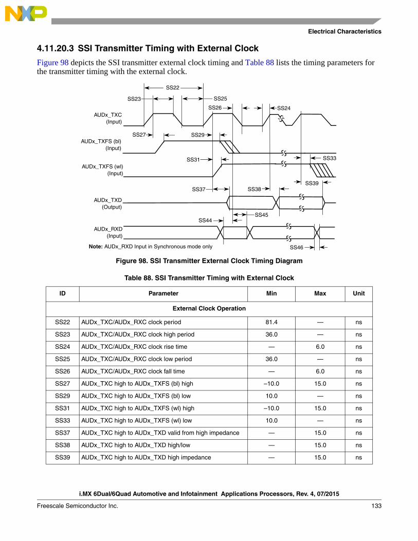
Electrical Characteristics
i.MX 6Dual/6Quad Automotive and Infotainment Applications Processors, Rev. 4, 07/2015
Freescale Semiconductor Inc. 133
4.11.20.3 SSI Transmitter Timing with External Clock
Figure 98 depicts the SSI transmitter external clock timing and Table 88 lists the timing parameters for the transmitter timing with the external clock.
Figure 98. SSI Transmitter External Clock Timing Diagram
Table 88. SSI Transmitter Timing with External Clock
ID Parameter Min Max Unit
External Clock Operation
SS22 AUDx_TXC/AUDx_RXC clock period 81.4 — ns
SS23 AUDx_TXC/AUDx_RXC clock high period 36.0 — ns
SS24 AUDx_TXC/AUDx_RXC clock rise time — 6.0 ns
SS25 AUDx_TXC/AUDx_RXC clock low period 36.0 — ns
SS26 AUDx_TXC/AUDx_RXC clock fall time — 6.0 ns
SS27 AUDx_TXC high to AUDx_TXFS (bl) high –10.0 15.0 ns
SS29 AUDx_TXC high to AUDx_TXFS (bl) low 10.0 — ns
SS31 AUDx_TXC high to AUDx_TXFS (wl) high –10.0 15.0 ns
SS33 AUDx_TXC high to AUDx_TXFS (wl) low 10.0 — ns
SS37 AUDx_TXC high to AUDx_TXD valid from high impedance — 15.0 ns
SS38 AUDx_TXC high to AUDx_TXD high/low — 15.0 ns
SS39 AUDx_TXC high to AUDx_TXD high impedance — 15.0 ns
SS45
SS33
SS24SS26
SS25SS23
Note: AUDx_RXD Input in Synchronous mode only
SS31
SS29SS27
SS22
SS44
SS39SS38SS37
SS46
AUDx_TXC(Input)
AUDx_TXFS (bl)(Input)
AUDx_TXFS (wl)(Input)
AUDx_TXD(Output)
AUDx_RXD(Input)
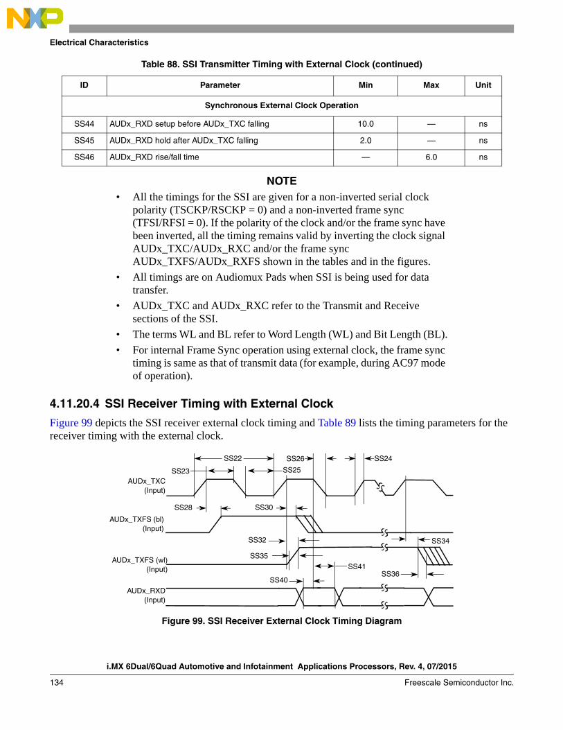
i.MX 6Dual/6Quad Automotive and Infotainment Applications Processors, Rev. 4, 07/2015
134 Freescale Semiconductor Inc.
Electrical Characteristics
NOTE• All the timings for the SSI are given for a non-inverted serial clock
polarity (TSCKP/RSCKP = 0) and a non-inverted frame sync (TFSI/RFSI = 0). If the polarity of the clock and/or the frame sync have been inverted, all the timing remains valid by inverting the clock signal AUDx_TXC/AUDx_RXC and/or the frame sync AUDx_TXFS/AUDx_RXFS shown in the tables and in the figures.
• All timings are on Audiomux Pads when SSI is being used for data transfer.
• AUDx_TXC and AUDx_RXC refer to the Transmit and Receive sections of the SSI.
• The terms WL and BL refer to Word Length (WL) and Bit Length (BL).
• For internal Frame Sync operation using external clock, the frame sync timing is same as that of transmit data (for example, during AC97 mode of operation).
4.11.20.4 SSI Receiver Timing with External Clock
Figure 99 depicts the SSI receiver external clock timing and Table 89 lists the timing parameters for the receiver timing with the external clock.
Figure 99. SSI Receiver External Clock Timing Diagram
Synchronous External Clock Operation
SS44 AUDx_RXD setup before AUDx_TXC falling 10.0 — ns
SS45 AUDx_RXD hold after AUDx_TXC falling 2.0 — ns
SS46 AUDx_RXD rise/fall time — 6.0 ns
Table 88. SSI Transmitter Timing with External Clock (continued)
ID Parameter Min Max Unit
SS24
SS34
SS35
SS30SS28
SS26
SS25SS23
SS40
SS22
SS32
SS36SS41
AUDx_TXC(Input)
AUDx_TXFS (bl)(Input)
AUDx_TXFS (wl)(Input)
AUDx_RXD(Input)
Electrical Characteristics
i.MX 6Dual/6Quad Automotive and Infotainment Applications Processors, Rev. 4, 07/2015
Freescale Semiconductor Inc. 135
NOTE• All the timings for the SSI are given for a non-inverted serial clock
polarity (TSCKP/RSCKP = 0) and a non-inverted frame sync (TFSI/RFSI = 0). If the polarity of the clock and/or the frame sync have been inverted, all the timing remains valid by inverting the clock signal AUDx_TXC/AUDx_RXC and/or the frame sync AUDx_TXFS/AUDx_RXFS shown in the tables and in the figures.
• All timings are on Audiomux Pads when SSI is being used for data transfer.
• AUDx_TXC and AUDx_RXC refer to the Transmit and Receive sections of the SSI.
• The terms, WL and BL, refer to Word Length (WL) and Bit Length(BL).
• For internal Frame Sync operation using external clock, the frame sync timing is same as that of transmit data (for example, during AC97 mode of operation).
Table 89. SSI Receiver Timing with External Clock
ID Parameter Min Max Unit
External Clock Operation
SS22 AUDx_TXC/AUDx_RXC clock period 81.4 — ns
SS23 AUDx_TXC/AUDx_RXC clock high period 36 — ns
SS24 AUDx_TXC/AUDx_RXC clock rise time — 6.0 ns
SS25 AUDx_TXC/AUDx_RXC clock low period 36 — ns
SS26 AUDx_TXC/AUDx_RXC clock fall time — 6.0 ns
SS28 AUDx_RXC high to AUDx_TXFS (bl) high –10 15.0 ns
SS30 AUDx_RXC high to AUDx_TXFS (bl) low 10 — ns
SS32 AUDx_RXC high to AUDx_TXFS (wl) high –10 15.0 ns
SS34 AUDx_RXC high to AUDx_TXFS (wl) low 10 — ns
SS35 AUDx_TXC/AUDx_RXC External AUDx_TXFS rise time — 6.0 ns
SS36 AUDx_TXC/AUDx_RXC External AUDx_TXFS fall time — 6.0 ns
SS40 AUDx_RXD setup time before AUDx_RXC low 10 — ns
SS41 AUDx_RXD hold time after AUDx_RXC low 2 — ns
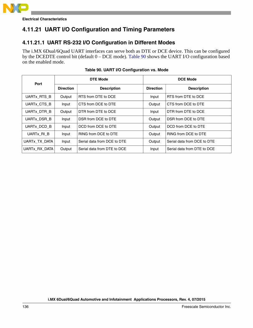
i.MX 6Dual/6Quad Automotive and Infotainment Applications Processors, Rev. 4, 07/2015
136 Freescale Semiconductor Inc.
Electrical Characteristics
4.11.21 UART I/O Configuration and Timing Parameters
4.11.21.1 UART RS-232 I/O Configuration in Different Modes
The i.MX 6Dual/6Quad UART interfaces can serve both as DTE or DCE device. This can be configured by the DCEDTE control bit (default 0 – DCE mode). Table 90 shows the UART I/O configuration based on the enabled mode.
Table 90. UART I/O Configuration vs. Mode
PortDTE Mode DCE Mode
Direction Description Direction Description
UARTx_RTS_B Output RTS from DTE to DCE Input RTS from DTE to DCE
UARTx_CTS_B Input CTS from DCE to DTE Output CTS from DCE to DTE
UARTx_DTR_B Output DTR from DTE to DCE Input DTR from DTE to DCE
UARTx_DSR_B Input DSR from DCE to DTE Output DSR from DCE to DTE
UARTx_DCD_B Input DCD from DCE to DTE Output DCD from DCE to DTE
UARTx_RI_B Input RING from DCE to DTE Output RING from DCE to DTE
UARTx_TX_DATA Input Serial data from DCE to DTE Output Serial data from DCE to DTE
UARTx_RX_DATA Output Serial data from DTE to DCE Input Serial data from DTE to DCE
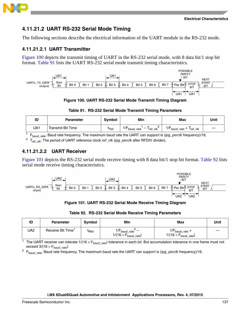
Electrical Characteristics
i.MX 6Dual/6Quad Automotive and Infotainment Applications Processors, Rev. 4, 07/2015
Freescale Semiconductor Inc. 137
4.11.21.2 UART RS-232 Serial Mode Timing
The following sections describe the electrical information of the UART module in the RS-232 mode.
4.11.21.2.1 UART Transmitter
Figure 100 depicts the transmit timing of UART in the RS-232 serial mode, with 8 data bit/1 stop bit format. Table 91 lists the UART RS-232 serial mode transmit timing characteristics.
Figure 100. UART RS-232 Serial Mode Transmit Timing Diagram
4.11.21.2.2 UART Receiver
Figure 101 depicts the RS-232 serial mode receive timing with 8 data bit/1 stop bit format. Table 92 lists serial mode receive timing characteristics.
Figure 101. UART RS-232 Serial Mode Receive Timing Diagram
Table 91. RS-232 Serial Mode Transmit Timing Parameters
ID Parameter Symbol Min Max Unit
UA1 Transmit Bit Time tTbit 1/Fbaud_rate1 – Tref_clk
2
1 Fbaud_rate: Baud rate frequency. The maximum baud rate the UART can support is (ipg_perclk frequency)/16.2 Tref_clk: The period of UART reference clock ref_clk (ipg_perclk after RFDIV divider).
1/Fbaud_rate + Tref_clk —
Table 92. RS-232 Serial Mode Receive Timing Parameters
ID Parameter Symbol Min Max Unit
UA2 Receive Bit Time1
1 The UART receiver can tolerate 1/(16 × Fbaud_rate) tolerance in each bit. But accumulation tolerance in one frame must not exceed 3/(16 × Fbaud_rate).
tRbit 1/Fbaud_rate2 –
1/(16 × Fbaud_rate)
2 Fbaud_rate: Baud rate frequency. The maximum baud rate the UART can support is (ipg_perclk frequency)/16.
1/Fbaud_rate + 1/(16 × Fbaud_rate)
—
Bit 1 Bit 2Bit 0 Bit 4 Bit 5 Bit 6 Bit 7UARTx_TX_DATA
(output) Bit 3StartBit
STOPBIT
NEXTSTART
BIT
POSSIBLEPARITY
BIT
Par Bit
UA1
UA1 UA1
UA1
Bit 1 Bit 2Bit 0 Bit 4 Bit 5 Bit 6 Bit 7UARTx_RX_DATA(input)
Bit 3StartBit STOP
BIT
NEXTSTART
BIT
POSSIBLEPARITY
BIT
Par Bit
UA2 UA2
UA2 UA2
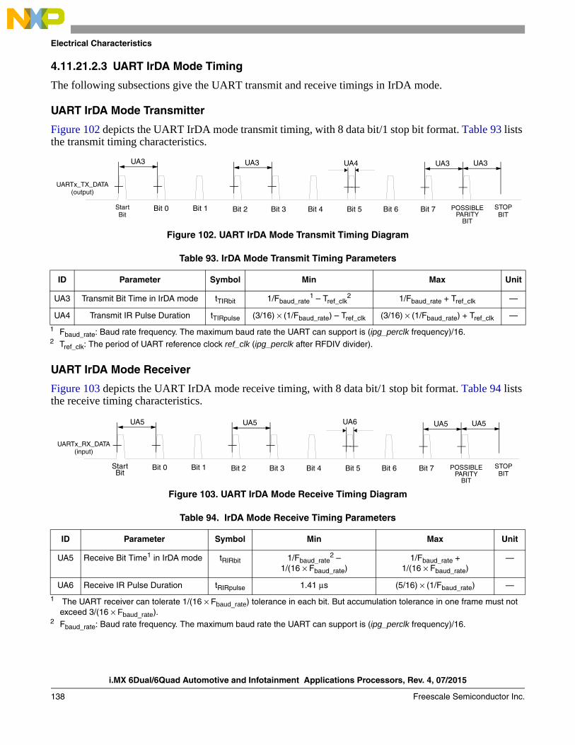
i.MX 6Dual/6Quad Automotive and Infotainment Applications Processors, Rev. 4, 07/2015
138 Freescale Semiconductor Inc.
Electrical Characteristics
4.11.21.2.3 UART IrDA Mode Timing
The following subsections give the UART transmit and receive timings in IrDA mode.
UART IrDA Mode Transmitter
Figure 102 depicts the UART IrDA mode transmit timing, with 8 data bit/1 stop bit format. Table 93 lists the transmit timing characteristics.
Figure 102. UART IrDA Mode Transmit Timing Diagram
UART IrDA Mode Receiver
Figure 103 depicts the UART IrDA mode receive timing, with 8 data bit/1 stop bit format. Table 94 lists the receive timing characteristics.
Figure 103. UART IrDA Mode Receive Timing Diagram
Table 93. IrDA Mode Transmit Timing Parameters
ID Parameter Symbol Min Max Unit
UA3 Transmit Bit Time in IrDA mode tTIRbit 1/Fbaud_rate1 – Tref_clk
2
1 Fbaud_rate: Baud rate frequency. The maximum baud rate the UART can support is (ipg_perclk frequency)/16.2 Tref_clk: The period of UART reference clock ref_clk (ipg_perclk after RFDIV divider).
1/Fbaud_rate + Tref_clk —
UA4 Transmit IR Pulse Duration tTIRpulse (3/16) × (1/Fbaud_rate) – Tref_clk (3/16) × (1/Fbaud_rate) + Tref_clk —
Table 94. IrDA Mode Receive Timing Parameters
ID Parameter Symbol Min Max Unit
UA5 Receive Bit Time1 in IrDA mode
1 The UART receiver can tolerate 1/(16 × Fbaud_rate) tolerance in each bit. But accumulation tolerance in one frame must not exceed 3/(16 × Fbaud_rate).
tRIRbit 1/Fbaud_rate2 –
1/(16 × Fbaud_rate)
2 Fbaud_rate: Baud rate frequency. The maximum baud rate the UART can support is (ipg_perclk frequency)/16.
1/Fbaud_rate + 1/(16 × Fbaud_rate)
—
UA6 Receive IR Pulse Duration tRIRpulse 1.41 μs (5/16) × (1/Fbaud_rate) —
Bit 1 Bit 2Bit 0 Bit 4 Bit 5 Bit 6 Bit 7
UARTx_TX_DATA(output)
Bit 3StartBit
STOPBIT
POSSIBLEPARITY
BIT
UA3 UA3 UA3 UA3UA4
Bit 1 Bit 2Bit 0 Bit 4 Bit 5 Bit 6 Bit 7Bit 3 STOPBIT
POSSIBLEPARITY
BIT
UA5 UA5 UA5 UA5UA6
StartBit
UARTx_RX_DATA(input)
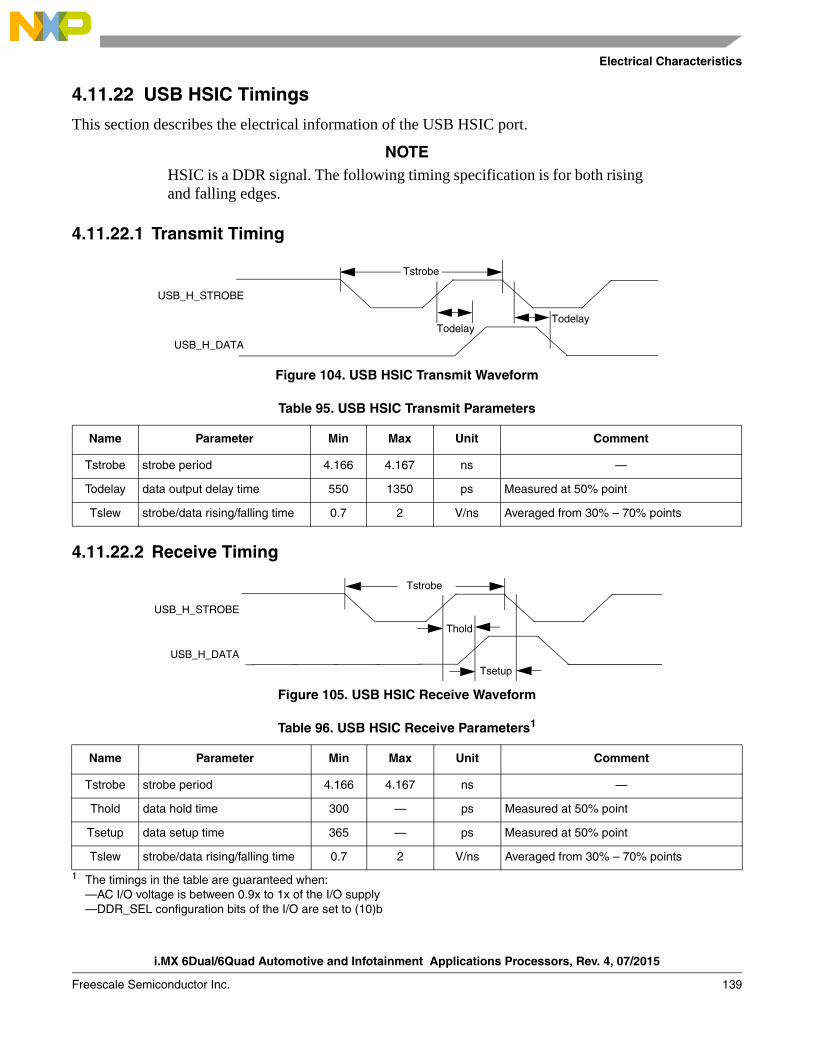
Electrical Characteristics
i.MX 6Dual/6Quad Automotive and Infotainment Applications Processors, Rev. 4, 07/2015
Freescale Semiconductor Inc. 139
4.11.22 USB HSIC Timings
This section describes the electrical information of the USB HSIC port.
NOTEHSIC is a DDR signal. The following timing specification is for both rising and falling edges.
4.11.22.1 Transmit Timing
Figure 104. USB HSIC Transmit Waveform
4.11.22.2 Receive Timing
Figure 105. USB HSIC Receive Waveform
Table 95. USB HSIC Transmit Parameters
Name Parameter Min Max Unit Comment
Tstrobe strobe period 4.166 4.167 ns —
Todelay data output delay time 550 1350 ps Measured at 50% point
Tslew strobe/data rising/falling time 0.7 2 V/ns Averaged from 30% – 70% points
Table 96. USB HSIC Receive Parameters1
1 The timings in the table are guaranteed when:—AC I/O voltage is between 0.9x to 1x of the I/O supply—DDR_SEL configuration bits of the I/O are set to (10)b
Name Parameter Min Max Unit Comment
Tstrobe strobe period 4.166 4.167 ns —
Thold data hold time 300 — ps Measured at 50% point
Tsetup data setup time 365 — ps Measured at 50% point
Tslew strobe/data rising/falling time 0.7 2 V/ns Averaged from 30% – 70% points
USB_H_STROBE
USB_H_DATA
Todelay
Tstrobe
Todelay
USB_H_STROBE
USB_H_DATA
Thold
Tstrobe
Tsetup
i.MX 6Dual/6Quad Automotive and Infotainment Applications Processors, Rev. 4, 07/2015
140 Freescale Semiconductor Inc.
Electrical Characteristics
4.11.23 USB PHY Parameters
This section describes the USB-OTG PHY and the USB Host port PHY parameters.
The USB PHY meets the electrical compliance requirements defined in the Universal Serial Bus Revision 2.0 OTG, USB Host with the amendments below (On-The-Go and Embedded Host Supplement to the USB Revision 2.0 Specification is not applicable to Host port).
• USB ENGINEERING CHANGE NOTICE
— Title: 5V Short Circuit Withstand Requirement Change
— Applies to: Universal Serial Bus Specification, Revision 2.0
• Errata for USB Revision 2.0 April 27, 2000 as of 12/7/2000
• USB ENGINEERING CHANGE NOTICE
— Title: Pull-up/Pull-down resistors
— Applies to: Universal Serial Bus Specification, Revision 2.0
• USB ENGINEERING CHANGE NOTICE
— Title: Suspend Current Limit Changes
— Applies to: Universal Serial Bus Specification, Revision 2.0
• USB ENGINEERING CHANGE NOTICE
— Title: USB 2.0 Phase Locked SOFs
— Applies to: Universal Serial Bus Specification, Revision 2.0
• On-The-Go and Embedded Host Supplement to the USB Revision 2.0 Specification
— Revision 2.0 plus errata and ecn June 4, 2010
• Battery Charging Specification (available from USB-IF)
— Revision 1.2, December 7, 2010
— Portable device only
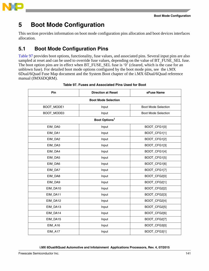
Boot Mode Configuration
i.MX 6Dual/6Quad Automotive and Infotainment Applications Processors, Rev. 4, 07/2015
Freescale Semiconductor Inc. 141
5 Boot Mode ConfigurationThis section provides information on boot mode configuration pins allocation and boot devices interfaces allocation.
5.1 Boot Mode Configuration PinsTable 97 provides boot options, functionality, fuse values, and associated pins. Several input pins are also sampled at reset and can be used to override fuse values, depending on the value of BT_FUSE_SEL fuse. The boot option pins are in effect when BT_FUSE_SEL fuse is ‘0’ (cleared, which is the case for an unblown fuse). For detailed boot mode options configured by the boot mode pins, see the i.MX 6Dual/6Quad Fuse Map document and the System Boot chapter of the i.MX 6Dual/6Quad reference manual (IMX6DQRM).
Table 97. Fuses and Associated Pins Used for Boot
Pin Direction at Reset eFuse Name
Boot Mode Selection
BOOT_MODE1 Input Boot Mode Selection
BOOT_MODE0 Input Boot Mode Selection
Boot Options1
EIM_DA0 Input BOOT_CFG1[0]
EIM_DA1 Input BOOT_CFG1[1]
EIM_DA2 Input BOOT_CFG1[2]
EIM_DA3 Input BOOT_CFG1[3]
EIM_DA4 Input BOOT_CFG1[4]
EIM_DA5 Input BOOT_CFG1[5]
EIM_DA6 Input BOOT_CFG1[6]
EIM_DA7 Input BOOT_CFG1[7]
EIM_DA8 Input BOOT_CFG2[0]
EIM_DA9 Input BOOT_CFG2[1]
EIM_DA10 Input BOOT_CFG2[2]
EIM_DA11 Input BOOT_CFG2[3]
EIM_DA12 Input BOOT_CFG2[4]
EIM_DA13 Input BOOT_CFG2[5]
EIM_DA14 Input BOOT_CFG2[6]
EIM_DA15 Input BOOT_CFG2[7]
EIM_A16 Input BOOT_CFG3[0]
EIM_A17 Input BOOT_CFG3[1]
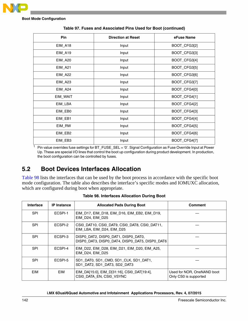
i.MX 6Dual/6Quad Automotive and Infotainment Applications Processors, Rev. 4, 07/2015
142 Freescale Semiconductor Inc.
Boot Mode Configuration
5.2 Boot Devices Interfaces AllocationTable 98 lists the interfaces that can be used by the boot process in accordance with the specific boot mode configuration. The table also describes the interface’s specific modes and IOMUXC allocation, which are configured during boot when appropriate.
EIM_A18 Input BOOT_CFG3[2]
EIM_A19 Input BOOT_CFG3[3]
EIM_A20 Input BOOT_CFG3[4]
EIM_A21 Input BOOT_CFG3[5]
EIM_A22 Input BOOT_CFG3[6]
EIM_A23 Input BOOT_CFG3[7]
EIM_A24 Input BOOT_CFG4[0]
EIM_WAIT Input BOOT_CFG4[1]
EIM_LBA Input BOOT_CFG4[2]
EIM_EB0 Input BOOT_CFG4[3]
EIM_EB1 Input BOOT_CFG4[4]
EIM_RW Input BOOT_CFG4[5]
EIM_EB2 Input BOOT_CFG4[6]
EIM_EB3 Input BOOT_CFG4[7]
1 Pin value overrides fuse settings for BT_FUSE_SEL = ‘0’. Signal Configuration as Fuse Override Input at Power Up. These are special I/O lines that control the boot up configuration during product development. In production, the boot configuration can be controlled by fuses.
Table 98. Interfaces Allocation During Boot
Interface IP Instance Allocated Pads During Boot Comment
SPI ECSPI-1 EIM_D17, EIM_D18, EIM_D16, EIM_EB2, EIM_D19, EIM_D24, EIM_D25
—
SPI ECSPI-2 CSI0_DAT10, CSI0_DAT9, CSI0_DAT8, CSI0_DAT11, EIM_LBA, EIM_D24, EIM_D25
—
SPI ECSPI-3 DISP0_DAT2, DISP0_DAT1, DISP0_DAT0, DISP0_DAT3, DISP0_DAT4, DISP0_DAT5, DISP0_DAT6
—
SPI ECSPI-4 EIM_D22, EIM_D28, EIM_D21, EIM_D20, EIM_A25, EIM_D24, EIM_D25
—
SPI ECSPI-5 SD1_DAT0, SD1_CMD, SD1_CLK, SD1_DAT1, SD1_DAT2, SD1_DAT3, SD2_DAT3
—
EIM EIM EIM_DA[15:0], EIM_D[31:16], CSI0_DAT[19:4], CSI0_DATA_EN, CSI0_VSYNC
Used for NOR, OneNAND bootOnly CS0 is supported
Table 97. Fuses and Associated Pins Used for Boot (continued)
Pin Direction at Reset eFuse Name
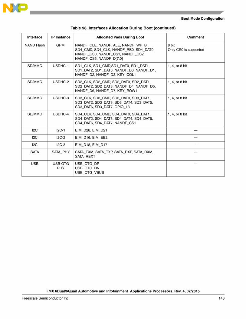
Boot Mode Configuration
i.MX 6Dual/6Quad Automotive and Infotainment Applications Processors, Rev. 4, 07/2015
Freescale Semiconductor Inc. 143
NAND Flash GPMI NANDF_CLE, NANDF_ALE, NANDF_WP_B, SD4_CMD, SD4_CLK, NANDF_RB0, SD4_DAT0, NANDF_CS0, NANDF_CS1, NANDF_CS2, NANDF_CS3, NANDF_D[7:0]
8 bitOnly CS0 is supported
SD/MMC USDHC-1 SD1_CLK, SD1_CMD,SD1_DAT0, SD1_DAT1, SD1_DAT2, SD1_DAT3, NANDF_D0, NANDF_D1, NANDF_D2, NANDF_D3, KEY_COL1
1, 4, or 8 bit
SD/MMC USDHC-2 SD2_CLK, SD2_CMD, SD2_DAT0, SD2_DAT1, SD2_DAT2, SD2_DAT3, NANDF_D4, NANDF_D5, NANDF_D6, NANDF_D7, KEY_ROW1
1, 4, or 8 bit
SD/MMC USDHC-3 SD3_CLK, SD3_CMD, SD3_DAT0, SD3_DAT1, SD3_DAT2, SD3_DAT3, SD3_DAT4, SD3_DAT5, SD3_DAT6, SD3_DAT7, GPIO_18
1, 4, or 8 bit
SD/MMC USDHC-4 SD4_CLK, SD4_CMD, SD4_DAT0, SD4_DAT1, SD4_DAT2, SD4_DAT3, SD4_DAT4, SD4_DAT5, SD4_DAT6, SD4_DAT7, NANDF_CS1
1, 4, or 8 bit
I2C I2C-1 EIM_D28, EIM_D21 —
I2C I2C-2 EIM_D16, EIM_EB2 —
I2C I2C-3 EIM_D18, EIM_D17 —
SATA SATA_PHY SATA_TXM, SATA_TXP, SATA_RXP, SATA_RXM, SATA_REXT
—
USB USB-OTG PHY
USB_OTG_DPUSB_OTG_DNUSB_OTG_VBUS
—
Table 98. Interfaces Allocation During Boot (continued)
Interface IP Instance Allocated Pads During Boot Comment
i.MX 6Dual/6Quad Automotive and Infotainment Applications Processors, Rev. 4, 07/2015
144 Freescale Semiconductor Inc.
Package Information and Contact Assignments
6 Package Information and Contact AssignmentsThis section includes the contact assignment information and mechanical package drawing.
6.1 Updated Signal Naming ConventionThe signal names of the i.MX6 series of products have been standardized to better align the signal names within the family and across the documentation. Some of the benefits of these changes are as follows:
• The names are unique within the scope of an SoC and within the series of products
• Searches will return all occurrences of the named signal
• The names are consistent between i.MX 6 series products implementing the same modules
• The module instance is incorporated into the signal name
This change applies only to signal names. The original ball names have been preserved to prevent the need to change schematics, BSDL models, IBIS models, etc.
Throughout this document, the updated signal names are used except where referenced as a ball name (such as the Functional Contact Assignments table, Ball Map table, and so on). A master list of the signal name changes is in the document, IMX 6 Series Signal Name Mapping (EB792). This list can be used to map the signal names used in older documentation to the new standardized naming conventions.
6.2 21 x 21 mm Package Information
6.2.1 Case FCPBGA, 21 x 21 mm, 0.8 mm Pitch, 25 x 25 Ball Matrix
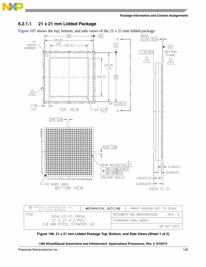
Package Information and Contact Assignments
i.MX 6Dual/6Quad Automotive and Infotainment Applications Processors, Rev. 4, 07/2015
Freescale Semiconductor Inc. 145
6.2.1.1 21 x 21 mm Lidded Package
Figure 107 shows the top, bottom, and side views of the 21 × 21 mm lidded package.
Figure 106. 21 x 21 mm Lidded Package Top, Bottom, and Side Views (Sheet 1 of 2)
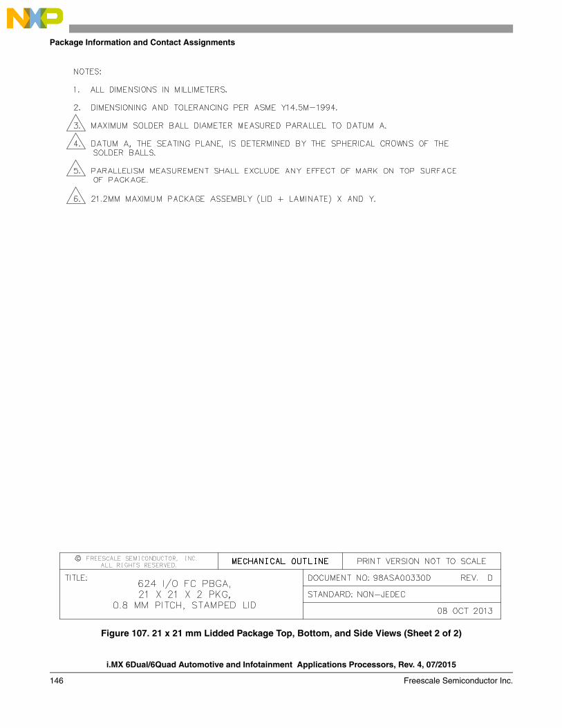
i.MX 6Dual/6Quad Automotive and Infotainment Applications Processors, Rev. 4, 07/2015
146 Freescale Semiconductor Inc.
Package Information and Contact Assignments
Figure 107. 21 x 21 mm Lidded Package Top, Bottom, and Side Views (Sheet 2 of 2)
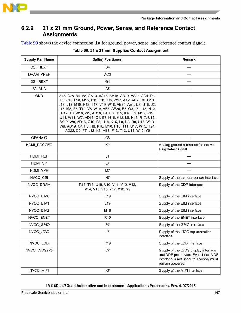
Package Information and Contact Assignments
i.MX 6Dual/6Quad Automotive and Infotainment Applications Processors, Rev. 4, 07/2015
Freescale Semiconductor Inc. 147
6.2.2 21 x 21 mm Ground, Power, Sense, and Reference Contact Assignments
Table 99 shows the device connection list for ground, power, sense, and reference contact signals.
Table 99. 21 x 21 mm Supplies Contact Assignment
Supply Rail Name Ball(s) Position(s) Remark
CSI_REXT D4 —
DRAM_VREF AC2 —
DSI_REXT G4 —
FA_ANA A5 —
GND A13, A25, A4, A8, AA10, AA13, AA16, AA19, AA22, AD4, D3, F8, J15, L10, M15, P15, T15, U8, W17, AA7, AD7, D6, G10,
J18, L12, M18, P18, T17, V19, W18, AB24, AE1, D8, G19, J2, L15, M8, P8, T19, V8, W19, AB3, AE25, E5, G3, J8, L18, N10,
R12, T8, W10, W3, AD10, B4, E6, H12, K10, L2, N15, R15, U11, W11, W7, AD13, C1, E7, H15, K12, L5, N18, R17, U12, W12, W8, AD16, C10, F5, H18, K15, L8, N8, R8, U15, W13, W9, AD19, C4, F6, H8, K18, M10, P10, T11, U17, W15, Y24,
AD22, C6, F7, J12, K8, M12, P12, T12, U19, W16, Y5
—
GPANAIO C8 —
HDMI_DDCCEC K2 Analog ground reference for the Hot Plug detect signal
HDMI_REF J1 —
HDMI_VP L7 —
HDMI_VPH M7 —
NVCC_CSI N7 Supply of the camera sensor interface
NVCC_DRAM R18, T18, U18, V10, V11, V12, V13,V14, V15, V16, V17, V18, V9
Supply of the DDR interface
NVCC_EIM0 K19 Supply of the EIM interface
NVCC_EIM1 L19 Supply of the EIM interface
NVCC_EIM2 M19 Supply of the EIM interface
NVCC_ENET R19 Supply of the ENET interface
NVCC_GPIO P7 Supply of the GPIO interface
NVCC_JTAG J7 Supply of the JTAG tap controller interface
NVCC_LCD P19 Supply of the LCD interface
NVCC_LVDS2P5 V7 Supply of the LVDS display interface and DDR pre-drivers. Even if the LVDS interface is not used, this supply must remain powered.
NVCC_MIPI K7 Supply of the MIPI interface
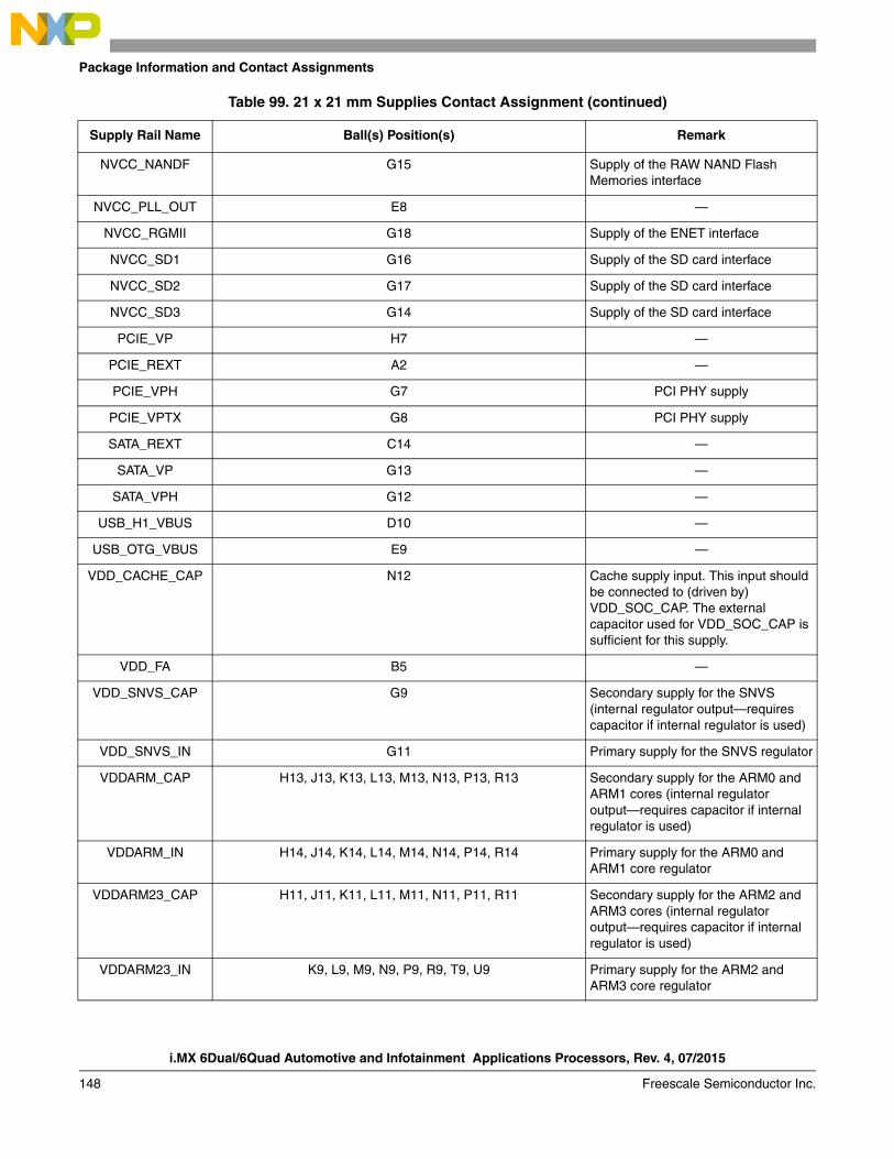
i.MX 6Dual/6Quad Automotive and Infotainment Applications Processors, Rev. 4, 07/2015
148 Freescale Semiconductor Inc.
Package Information and Contact Assignments
NVCC_NANDF G15 Supply of the RAW NAND Flash Memories interface
NVCC_PLL_OUT E8 —
NVCC_RGMII G18 Supply of the ENET interface
NVCC_SD1 G16 Supply of the SD card interface
NVCC_SD2 G17 Supply of the SD card interface
NVCC_SD3 G14 Supply of the SD card interface
PCIE_VP H7 —
PCIE_REXT A2 —
PCIE_VPH G7 PCI PHY supply
PCIE_VPTX G8 PCI PHY supply
SATA_REXT C14 —
SATA_VP G13 —
SATA_VPH G12 —
USB_H1_VBUS D10 —
USB_OTG_VBUS E9 —
VDD_CACHE_CAP N12 Cache supply input. This input should be connected to (driven by) VDD_SOC_CAP. The external capacitor used for VDD_SOC_CAP is sufficient for this supply.
VDD_FA B5 —
VDD_SNVS_CAP G9 Secondary supply for the SNVS (internal regulator output—requires capacitor if internal regulator is used)
VDD_SNVS_IN G11 Primary supply for the SNVS regulator
VDDARM_CAP H13, J13, K13, L13, M13, N13, P13, R13 Secondary supply for the ARM0 and ARM1 cores (internal regulator output—requires capacitor if internal regulator is used)
VDDARM_IN H14, J14, K14, L14, M14, N14, P14, R14 Primary supply for the ARM0 and ARM1 core regulator
VDDARM23_CAP H11, J11, K11, L11, M11, N11, P11, R11 Secondary supply for the ARM2 and ARM3 cores (internal regulator output—requires capacitor if internal regulator is used)
VDDARM23_IN K9, L9, M9, N9, P9, R9, T9, U9 Primary supply for the ARM2 and ARM3 core regulator
Table 99. 21 x 21 mm Supplies Contact Assignment (continued)
Supply Rail Name Ball(s) Position(s) Remark
Package Information and Contact Assignments
i.MX 6Dual/6Quad Automotive and Infotainment Applications Processors, Rev. 4, 07/2015
Freescale Semiconductor Inc. 149
Table 100 displays an alpha-sorted list of the signal assignments including power rails. The table also includes out of reset pad state.
VDDHIGH_CAP H10, J10 Secondary supply for the 2.5 V domain (internal regulator output—requires capacitor if internal regulator is used)
VDDHIGH_IN H9, J9 Primary supply for the 2.5 V regulator
VDDPU_CAP H17, J17, K17, L17, M17, N17, P17 Secondary supply for the VPU and GPU (internal regulator output—requires capacitor if internal regulator is used)
VDDSOC_CAP R10, T10, T13, T14, U10, U13, U14 Secondary supply for the SoC and PU (internal regulator output—requires capacitor if internal regulator is used)
VDDSOC_IN H16, J16, K16, L16, M16, N16, P16, R16, T16, U16 Primary supply for the SoC and PU regulators
VDDUSB_CAP F9 Secondary supply for the 3 V domain (internal regulator output—requires capacitor if internal regulator is used)
ZQPAD AE17 —
Table 100. 21 x 21 mm Functional Contact Assignments
Ball Name Ball Power Group Ball Type
Out of Reset Condition1
Default Mode (Reset Mode)
Default Function(Signal Name)
Input/Output Value2
BOOT_MODE0 C12 VDD_SNVS_IN GPIO ALT0 SRC_BOOT_MODE0 Input PD (100K)
BOOT_MODE1 F12 VDD_SNVS_IN GPIO ALT0 SRC_BOOT_MODE1 Input PD (100K)
CLK1_N C7 VDD_HIGH_CAP — — CLK1_N — —
CLK1_P D7 VDD_HIGH_CAP — — CLK1_P — —
CLK2_N C5 VDD_HIGH_CAP — — CLK2_N — —
CLK2_P D5 VDD_HIGH_CAP — — CLK2_P — —
CSI_CLK0M F4 NVCC_MIPI — — CSI_CLK_N — —
CSI_CLK0P F3 NVCC_MIPI — — CSI_CLK_P — —
CSI_D0M E4 NVCC_MIPI — — CSI_DATA0_N — —
CSI_D0P E3 NVCC_MIPI — — CSI_DATA0_P — —
CSI_D1M D1 NVCC_MIPI — — CSI_DATA1_N — —
CSI_D1P D2 NVCC_MIPI — — CSI_DATA1_P — —
CSI_D2M E1 NVCC_MIPI — — CSI_DATA2_N — —
CSI_D2P E2 NVCC_MIPI — — CSI_DATA2_P — —
CSI_D3M F2 NVCC_MIPI — — CSI_DATA3_N — —
Table 99. 21 x 21 mm Supplies Contact Assignment (continued)
Supply Rail Name Ball(s) Position(s) Remark
i.MX 6Dual/6Quad Automotive and Infotainment Applications Processors, Rev. 4, 07/2015
150 Freescale Semiconductor Inc.
Package Information and Contact Assignments
CSI_D3P F1 NVCC_MIPI — — CSI_DATA3_P — —
CSI0_DAT10 M1 NVCC_CSI GPIO ALT5 GPIO5_IO28 Input PU (100K)
CSI0_DAT11 M3 NVCC_CSI GPIO ALT5 GPIO5_IO29 Input PU (100K)
CSI0_DAT12 M2 NVCC_CSI GPIO ALT5 GPIO5_IO30 Input PU (100K)
CSI0_DAT13 L1 NVCC_CSI GPIO ALT5 GPIO5_IO31 Input PU (100K)
CSI0_DAT14 M4 NVCC_CSI GPIO ALT5 GPIO6_IO00 Input PU (100K)
CSI0_DAT15 M5 NVCC_CSI GPIO ALT5 GPIO6_IO01 Input PU (100K)
CSI0_DAT16 L4 NVCC_CSI GPIO ALT5 GPIO6_IO02 Input PU (100K)
CSI0_DAT17 L3 NVCC_CSI GPIO ALT5 GPIO6_IO03 Input PU (100K)
CSI0_DAT18 M6 NVCC_CSI GPIO ALT5 GPIO6_IO04 Input PU (100K)
CSI0_DAT19 L6 NVCC_CSI GPIO ALT5 GPIO6_IO05 Input PU (100K)
CSI0_DAT4 N1 NVCC_CSI GPIO ALT5 GPIO5_IO22 Input PU (100K)
CSI0_DAT5 P2 NVCC_CSI GPIO ALT5 GPIO5_IO23 Input PU (100K)
CSI0_DAT6 N4 NVCC_CSI GPIO ALT5 GPIO5_IO24 Input PU (100K)
CSI0_DAT7 N3 NVCC_CSI GPIO ALT5 GPIO5_IO25 Input PU (100K)
CSI0_DAT8 N6 NVCC_CSI GPIO ALT5 GPIO5_IO26 Input PU (100K)
CSI0_DAT9 N5 NVCC_CSI GPIO ALT5 GPIO5_IO27 Input PU (100K)
CSI0_DATA_EN P3 NVCC_CSI GPIO ALT5 GPIO5_IO20 Input PU (100K)
CSI0_MCLK P4 NVCC_CSI GPIO ALT5 GPIO5_IO19 Input PU (100K)
CSI0_PIXCLK P1 NVCC_CSI GPIO ALT5 GPIO5_IO18 Input PU (100K)
CSI0_VSYNC N2 NVCC_CSI GPIO ALT5 GPIO5_IO21 Input PU (100K)
DI0_DISP_CLK N19 NVCC_LCD GPIO ALT5 GPIO4_IO16 Input PU (100K)
DI0_PIN15 N21 NVCC_LCD GPIO ALT5 GPIO4_IO17 Input PU (100K)
DI0_PIN2 N25 NVCC_LCD GPIO ALT5 GPIO4_IO18 Input PU (100K)
DI0_PIN3 N20 NVCC_LCD GPIO ALT5 GPIO4_IO19 Input PU (100K)
DI0_PIN4 P25 NVCC_LCD GPIO ALT5 GPIO4_IO20 Input PU (100K)
DISP0_DAT0 P24 NVCC_LCD GPIO ALT5 GPIO4_IO21 Input PU (100K)
DISP0_DAT1 P22 NVCC_LCD GPIO ALT5 GPIO4_IO22 Input PU (100K)
DISP0_DAT10 R21 NVCC_LCD GPIO ALT5 GPIO4_IO31 Input PU (100K)
DISP0_DAT11 T23 NVCC_LCD GPIO ALT5 GPIO5_IO05 Input PU (100K)
DISP0_DAT12 T24 NVCC_LCD GPIO ALT5 GPIO5_IO06 Input PU (100K)
DISP0_DAT13 R20 NVCC_LCD GPIO ALT5 GPIO5_IO07 Input PU (100K)
DISP0_DAT14 U25 NVCC_LCD GPIO ALT5 GPIO5_IO08 Input PU (100K)
DISP0_DAT15 T22 NVCC_LCD GPIO ALT5 GPIO5_IO09 Input PU (100K)
DISP0_DAT16 T21 NVCC_LCD GPIO ALT5 GPIO5_IO10 Input PU (100K)
DISP0_DAT17 U24 NVCC_LCD GPIO ALT5 GPIO5_IO11 Input PU (100K)
Table 100. 21 x 21 mm Functional Contact Assignments (continued)
Ball Name Ball Power Group Ball Type
Out of Reset Condition1
Default Mode (Reset Mode)
Default Function(Signal Name)
Input/Output Value2
Package Information and Contact Assignments
i.MX 6Dual/6Quad Automotive and Infotainment Applications Processors, Rev. 4, 07/2015
Freescale Semiconductor Inc. 151
DISP0_DAT18 V25 NVCC_LCD GPIO ALT5 GPIO5_IO12 Input PU (100K)
DISP0_DAT19 U23 NVCC_LCD GPIO ALT5 GPIO5_IO13 Input PU (100K)
DISP0_DAT2 P23 NVCC_LCD GPIO ALT5 GPIO4_IO23 Input PU (100K)
DISP0_DAT20 U22 NVCC_LCD GPIO ALT5 GPIO5_IO14 Input PU (100K)
DISP0_DAT21 T20 NVCC_LCD GPIO ALT5 GPIO5_IO15 Input PU (100K)
DISP0_DAT22 V24 NVCC_LCD GPIO ALT5 GPIO5_IO16 Input PU (100K)
DISP0_DAT23 W24 NVCC_LCD GPIO ALT5 GPIO5_IO17 Input PU (100K)
DISP0_DAT3 P21 NVCC_LCD GPIO ALT5 GPIO4_IO24 Input PU (100K)
DISP0_DAT4 P20 NVCC_LCD GPIO ALT5 GPIO4_IO25 Input PU (100K)
DISP0_DAT5 R25 NVCC_LCD GPIO ALT5 GPIO4_IO26 Input PU (100K)
DISP0_DAT6 R23 NVCC_LCD GPIO ALT5 GPIO4_IO27 Input PU (100K)
DISP0_DAT7 R24 NVCC_LCD GPIO ALT5 GPIO4_IO28 Input PU (100K)
DISP0_DAT8 R22 NVCC_LCD GPIO ALT5 GPIO4_IO29 Input PU (100K)
DISP0_DAT9 T25 NVCC_LCD GPIO ALT5 GPIO4_IO30 Input PU (100K)
DRAM_A0 AC14 NVCC_DRAM DDR ALT0 DRAM_ADDR00 Output 0
DRAM_A1 AB14 NVCC_DRAM DDR ALT0 DRAM_ADDR01 Output 0
DRAM_A10 AA15 NVCC_DRAM DDR ALT0 DRAM_ADDR10 Output 0
DRAM_A11 AC12 NVCC_DRAM DDR ALT0 DRAM_ADDR11 Output 0
DRAM_A12 AD12 NVCC_DRAM DDR ALT0 DRAM_ADDR12 Output 0
DRAM_A13 AC17 NVCC_DRAM DDR ALT0 DRAM_ADDR13 Output 0
DRAM_A14 AA12 NVCC_DRAM DDR ALT0 DRAM_ADDR14 Output 0
DRAM_A15 Y12 NVCC_DRAM DDR ALT0 DRAM_ADDR15 Output 0
DRAM_A2 AA14 NVCC_DRAM DDR ALT0 DRAM_ADDR02 Output 0
DRAM_A3 Y14 NVCC_DRAM DDR ALT0 DRAM_ADDR03 Output 0
DRAM_A4 W14 NVCC_DRAM DDR ALT0 DRAM_ADDR04 Output 0
DRAM_A5 AE13 NVCC_DRAM DDR ALT0 DRAM_ADDR05 Output 0
DRAM_A6 AC13 NVCC_DRAM DDR ALT0 DRAM_ADDR06 Output 0
DRAM_A7 Y13 NVCC_DRAM DDR ALT0 DRAM_ADDR07 Output 0
DRAM_A8 AB13 NVCC_DRAM DDR ALT0 DRAM_ADDR08 Output 0
DRAM_A9 AE12 NVCC_DRAM DDR ALT0 DRAM_ADDR09 Output 0
DRAM_CAS AE16 NVCC_DRAM DDR ALT0 DRAM_CAS_B Output 0
DRAM_CS0 Y16 NVCC_DRAM DDR ALT0 DRAM_CS0_B Output 0
DRAM_CS1 AD17 NVCC_DRAM DDR ALT0 DRAM_CS1_B Output 0
DRAM_D0 AD2 NVCC_DRAM DDR ALT0 DRAM_DATA00 Input PU (100K)
DRAM_D1 AE2 NVCC_DRAM DDR ALT0 DRAM_DATA01 Input PU (100K)
DRAM_D10 AA6 NVCC_DRAM DDR ALT0 DRAM_DATA10 Input PU (100K)
Table 100. 21 x 21 mm Functional Contact Assignments (continued)
Ball Name Ball Power Group Ball Type
Out of Reset Condition1
Default Mode (Reset Mode)
Default Function(Signal Name)
Input/Output Value2
i.MX 6Dual/6Quad Automotive and Infotainment Applications Processors, Rev. 4, 07/2015
152 Freescale Semiconductor Inc.
Package Information and Contact Assignments
DRAM_D11 AE7 NVCC_DRAM DDR ALT0 DRAM_DATA11 Input PU (100K)
DRAM_D12 AB5 NVCC_DRAM DDR ALT0 DRAM_DATA12 Input PU (100K)
DRAM_D13 AC5 NVCC_DRAM DDR ALT0 DRAM_DATA13 Input PU (100K)
DRAM_D14 AB6 NVCC_DRAM DDR ALT0 DRAM_DATA14 Input PU (100K)
DRAM_D15 AC7 NVCC_DRAM DDR ALT0 DRAM_DATA15 Input PU (100K)
DRAM_D16 AB7 NVCC_DRAM DDR ALT0 DRAM_DATA16 Input PU (100K)
DRAM_D17 AA8 NVCC_DRAM DDR ALT0 DRAM_DATA17 Input PU (100K)
DRAM_D18 AB9 NVCC_DRAM DDR ALT0 DRAM_DATA18 Input PU (100K)
DRAM_D19 Y9 NVCC_DRAM DDR ALT0 DRAM_DATA19 Input PU (100K)
DRAM_D2 AC4 NVCC_DRAM DDR ALT0 DRAM_DATA02 Input PU (100K)
DRAM_D20 Y7 NVCC_DRAM DDR ALT0 DRAM_DATA20 Input PU (100K)
DRAM_D21 Y8 NVCC_DRAM DDR ALT0 DRAM_DATA21 Input PU (100K)
DRAM_D22 AC8 NVCC_DRAM DDR ALT0 DRAM_DATA22 Input PU (100K)
DRAM_D23 AA9 NVCC_DRAM DDR ALT0 DRAM_DATA23 Input PU (100K)
DRAM_D24 AE9 NVCC_DRAM DDR ALT0 DRAM_DATA24 Input PU (100K)
DRAM_D25 Y10 NVCC_DRAM DDR ALT0 DRAM_DATA25 Input PU (100K)
DRAM_D26 AE11 NVCC_DRAM DDR ALT0 DRAM_DATA26 Input PU (100K)
DRAM_D27 AB11 NVCC_DRAM DDR ALT0 DRAM_DATA27 Input PU (100K)
DRAM_D28 AC9 NVCC_DRAM DDR ALT0 DRAM_DATA28 Input PU (100K)
DRAM_D29 AD9 NVCC_DRAM DDR ALT0 DRAM_DATA29 Input PU (100K)
DRAM_D3 AA5 NVCC_DRAM DDR ALT0 DRAM_DATA03 Input PU (100K)
DRAM_D30 AD11 NVCC_DRAM DDR ALT0 DRAM_DATA30 Input PU (100K)
DRAM_D31 AC11 NVCC_DRAM DDR ALT0 DRAM_DATA31 Input PU (100K)
DRAM_D32 AA17 NVCC_DRAM DDR ALT0 DRAM_DATA32 Input PU (100K)
DRAM_D33 AA18 NVCC_DRAM DDR ALT0 DRAM_DATA33 Input PU (100K)
DRAM_D34 AC18 NVCC_DRAM DDR ALT0 DRAM_DATA34 Input PU (100K)
DRAM_D35 AE19 NVCC_DRAM DDR ALT0 DRAM_DATA35 Input PU (100K)
DRAM_D36 Y17 NVCC_DRAM DDR ALT0 DRAM_DATA36 Input PU (100K)
DRAM_D37 Y18 NVCC_DRAM DDR ALT0 DRAM_DATA37 Input PU (100K)
DRAM_D38 AB19 NVCC_DRAM DDR ALT0 DRAM_DATA38 Input PU (100K)
DRAM_D39 AC19 NVCC_DRAM DDR ALT0 DRAM_DATA39 Input PU (100K)
DRAM_D4 AC1 NVCC_DRAM DDR ALT0 DRAM_DATA04 Input PU (100K)
DRAM_D40 Y19 NVCC_DRAM DDR ALT0 DRAM_DATA40 Input PU (100K)
DRAM_D41 AB20 NVCC_DRAM DDR ALT0 DRAM_DATA41 Input PU (100K)
DRAM_D42 AB21 NVCC_DRAM DDR ALT0 DRAM_DATA42 Input PU (100K)
DRAM_D43 AD21 NVCC_DRAM DDR ALT0 DRAM_DATA43 Input PU (100K)
Table 100. 21 x 21 mm Functional Contact Assignments (continued)
Ball Name Ball Power Group Ball Type
Out of Reset Condition1
Default Mode (Reset Mode)
Default Function(Signal Name)
Input/Output Value2
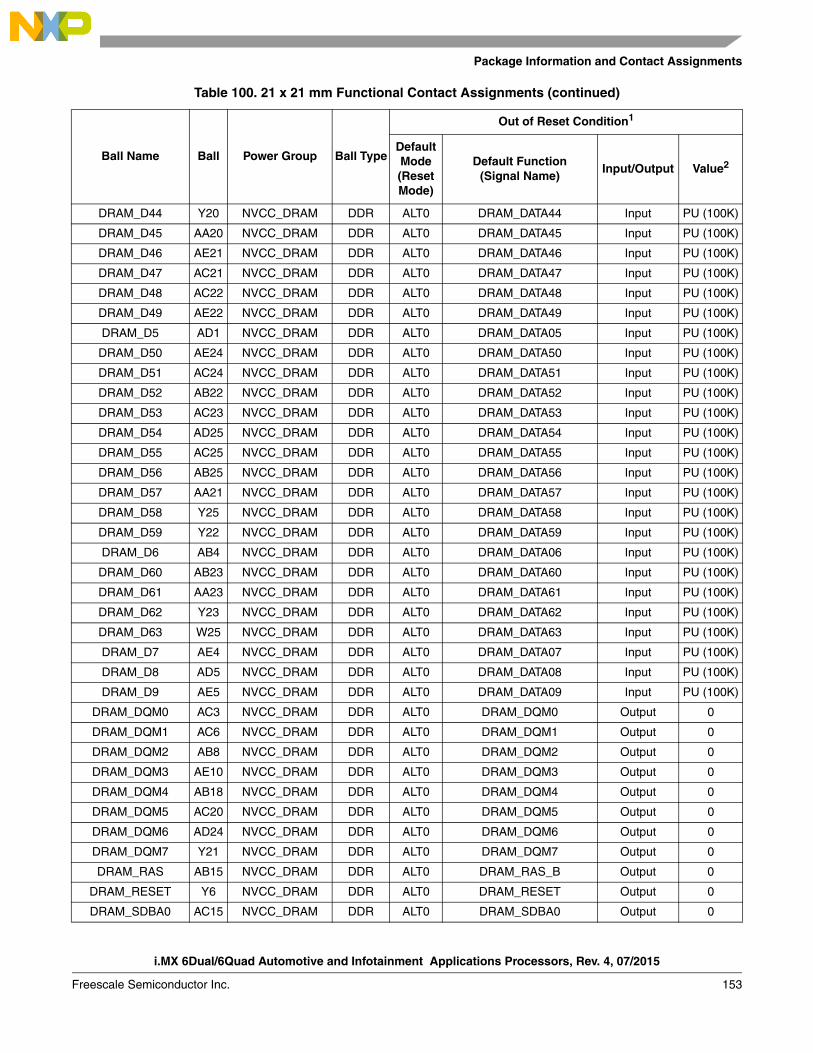
Package Information and Contact Assignments
i.MX 6Dual/6Quad Automotive and Infotainment Applications Processors, Rev. 4, 07/2015
Freescale Semiconductor Inc. 153
DRAM_D44 Y20 NVCC_DRAM DDR ALT0 DRAM_DATA44 Input PU (100K)
DRAM_D45 AA20 NVCC_DRAM DDR ALT0 DRAM_DATA45 Input PU (100K)
DRAM_D46 AE21 NVCC_DRAM DDR ALT0 DRAM_DATA46 Input PU (100K)
DRAM_D47 AC21 NVCC_DRAM DDR ALT0 DRAM_DATA47 Input PU (100K)
DRAM_D48 AC22 NVCC_DRAM DDR ALT0 DRAM_DATA48 Input PU (100K)
DRAM_D49 AE22 NVCC_DRAM DDR ALT0 DRAM_DATA49 Input PU (100K)
DRAM_D5 AD1 NVCC_DRAM DDR ALT0 DRAM_DATA05 Input PU (100K)
DRAM_D50 AE24 NVCC_DRAM DDR ALT0 DRAM_DATA50 Input PU (100K)
DRAM_D51 AC24 NVCC_DRAM DDR ALT0 DRAM_DATA51 Input PU (100K)
DRAM_D52 AB22 NVCC_DRAM DDR ALT0 DRAM_DATA52 Input PU (100K)
DRAM_D53 AC23 NVCC_DRAM DDR ALT0 DRAM_DATA53 Input PU (100K)
DRAM_D54 AD25 NVCC_DRAM DDR ALT0 DRAM_DATA54 Input PU (100K)
DRAM_D55 AC25 NVCC_DRAM DDR ALT0 DRAM_DATA55 Input PU (100K)
DRAM_D56 AB25 NVCC_DRAM DDR ALT0 DRAM_DATA56 Input PU (100K)
DRAM_D57 AA21 NVCC_DRAM DDR ALT0 DRAM_DATA57 Input PU (100K)
DRAM_D58 Y25 NVCC_DRAM DDR ALT0 DRAM_DATA58 Input PU (100K)
DRAM_D59 Y22 NVCC_DRAM DDR ALT0 DRAM_DATA59 Input PU (100K)
DRAM_D6 AB4 NVCC_DRAM DDR ALT0 DRAM_DATA06 Input PU (100K)
DRAM_D60 AB23 NVCC_DRAM DDR ALT0 DRAM_DATA60 Input PU (100K)
DRAM_D61 AA23 NVCC_DRAM DDR ALT0 DRAM_DATA61 Input PU (100K)
DRAM_D62 Y23 NVCC_DRAM DDR ALT0 DRAM_DATA62 Input PU (100K)
DRAM_D63 W25 NVCC_DRAM DDR ALT0 DRAM_DATA63 Input PU (100K)
DRAM_D7 AE4 NVCC_DRAM DDR ALT0 DRAM_DATA07 Input PU (100K)
DRAM_D8 AD5 NVCC_DRAM DDR ALT0 DRAM_DATA08 Input PU (100K)
DRAM_D9 AE5 NVCC_DRAM DDR ALT0 DRAM_DATA09 Input PU (100K)
DRAM_DQM0 AC3 NVCC_DRAM DDR ALT0 DRAM_DQM0 Output 0
DRAM_DQM1 AC6 NVCC_DRAM DDR ALT0 DRAM_DQM1 Output 0
DRAM_DQM2 AB8 NVCC_DRAM DDR ALT0 DRAM_DQM2 Output 0
DRAM_DQM3 AE10 NVCC_DRAM DDR ALT0 DRAM_DQM3 Output 0
DRAM_DQM4 AB18 NVCC_DRAM DDR ALT0 DRAM_DQM4 Output 0
DRAM_DQM5 AC20 NVCC_DRAM DDR ALT0 DRAM_DQM5 Output 0
DRAM_DQM6 AD24 NVCC_DRAM DDR ALT0 DRAM_DQM6 Output 0
DRAM_DQM7 Y21 NVCC_DRAM DDR ALT0 DRAM_DQM7 Output 0
DRAM_RAS AB15 NVCC_DRAM DDR ALT0 DRAM_RAS_B Output 0
DRAM_RESET Y6 NVCC_DRAM DDR ALT0 DRAM_RESET Output 0
DRAM_SDBA0 AC15 NVCC_DRAM DDR ALT0 DRAM_SDBA0 Output 0
Table 100. 21 x 21 mm Functional Contact Assignments (continued)
Ball Name Ball Power Group Ball Type
Out of Reset Condition1
Default Mode (Reset Mode)
Default Function(Signal Name)
Input/Output Value2
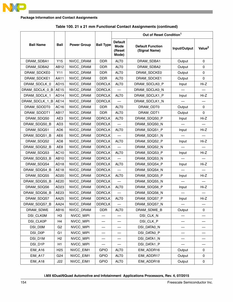
i.MX 6Dual/6Quad Automotive and Infotainment Applications Processors, Rev. 4, 07/2015
154 Freescale Semiconductor Inc.
Package Information and Contact Assignments
DRAM_SDBA1 Y15 NVCC_DRAM DDR ALT0 DRAM_SDBA1 Output 0
DRAM_SDBA2 AB12 NVCC_DRAM DDR ALT0 DRAM_SDBA2 Output 0
DRAM_SDCKE0 Y11 NVCC_DRAM DDR ALT0 DRAM_SDCKE0 Output 0
DRAM_SDCKE1 AA11 NVCC_DRAM DDR ALT0 DRAM_SDCKE1 Output 0
DRAM_SDCLK_0 AD15 NVCC_DRAM DDRCLK ALT0 DRAM_SDCLK0_P Input Hi-Z
DRAM_SDCLK_0_B AE15 NVCC_DRAM DDRCLK — DRAM_SDCLK0_N — —
DRAM_SDCLK_1 AD14 NVCC_DRAM DDRCLK ALT0 DRAM_SDCLK1_P Input Hi-Z
DRAM_SDCLK_1_B AE14 NVCC_DRAM DDRCLK — DRAM_SDCLK1_N — —
DRAM_SDODT0 AC16 NVCC_DRAM DDR ALT0 DRAM_ODT0 Output 0
DRAM_SDODT1 AB17 NVCC_DRAM DDR ALT0 DRAM_ODT1 Output 0
DRAM_SDQS0 AE3 NVCC_DRAM DDRCLK ALT0 DRAM_SDQS0_P Input Hi-Z
DRAM_SDQS0_B AD3 NVCC_DRAM DDRCLK — DRAM_SDQS0_N — —
DRAM_SDQS1 AD6 NVCC_DRAM DDRCLK ALT0 DRAM_SDQS1_P Input Hi-Z
DRAM_SDQS1_B AE6 NVCC_DRAM DDRCLK — DRAM_SDQS1_N — —
DRAM_SDQS2 AD8 NVCC_DRAM DDRCLK ALT0 DRAM_SDQS2_P Input Hi-Z
DRAM_SDQS2_B AE8 NVCC_DRAM DDRCLK — DRAM_SDQS2_N — —
DRAM_SDQS3 AC10 NVCC_DRAM DDRCLK ALT0 DRAM_SDQS3_P Input Hi-Z
DRAM_SDQS3_B AB10 NVCC_DRAM DDRCLK — DRAM_SDQS3_N — —
DRAM_SDQS4 AD18 NVCC_DRAM DDRCLK ALT0 DRAM_SDQS4_P Input Hi-Z
DRAM_SDQS4_B AE18 NVCC_DRAM DDRCLK — DRAM_SDQS4_N — —
DRAM_SDQS5 AD20 NVCC_DRAM DDRCLK ALT0 DRAM_SDQS5_P Input Hi-Z
DRAM_SDQS5_B AE20 NVCC_DRAM DDRCLK — DRAM_SDQS5_N — —
DRAM_SDQS6 AD23 NVCC_DRAM DDRCLK ALT0 DRAM_SDQS6_P Input Hi-Z
DRAM_SDQS6_B AE23 NVCC_DRAM DDRCLK — DRAM_SDQS6_N — —
DRAM_SDQS7 AA25 NVCC_DRAM DDRCLK ALT0 DRAM_SDQS7_P Input Hi-Z
DRAM_SDQS7_B AA24 NVCC_DRAM DDRCLK — DRAM_SDQS7_N — —
DRAM_SDWE AB16 NVCC_DRAM DDR ALT0 DRAM_SDWE_B Output 0
DSI_CLK0M H3 NVCC_MIPI — — DSI_CLK_N — —
DSI_CLK0P H4 NVCC_MIPI — — DSI_CLK_P — —
DSI_D0M G2 NVCC_MIPI — — DSI_DATA0_N — —
DSI_D0P G1 NVCC_MIPI — — DSI_DATA0_P — —
DSI_D1M H2 NVCC_MIPI — — DSI_DATA1_N — —
DSI_D1P H1 NVCC_MIPI — — DSI_DATA1_P — —
EIM_A16 H25 NVCC_EIM1 GPIO ALT0 EIM_ADDR16 Output 0
EIM_A17 G24 NVCC_EIM1 GPIO ALT0 EIM_ADDR17 Output 0
EIM_A18 J22 NVCC_EIM1 GPIO ALT0 EIM_ADDR18 Output 0
Table 100. 21 x 21 mm Functional Contact Assignments (continued)
Ball Name Ball Power Group Ball Type
Out of Reset Condition1
Default Mode (Reset Mode)
Default Function(Signal Name)
Input/Output Value2
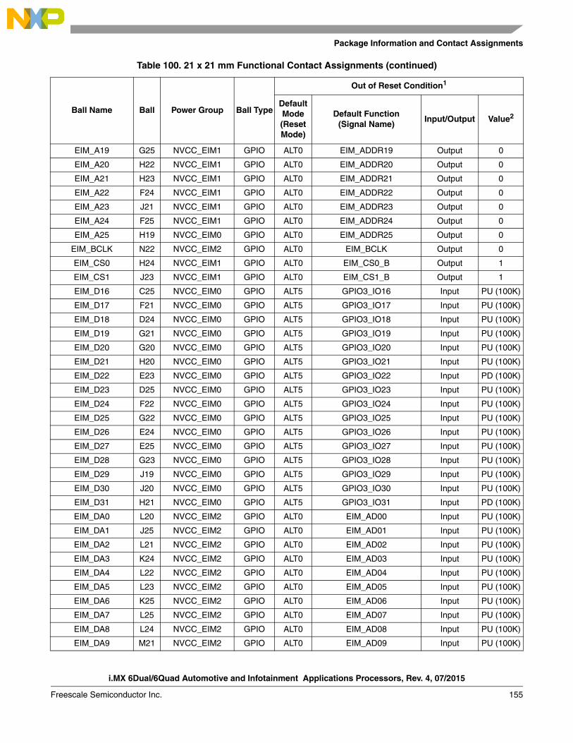
Package Information and Contact Assignments
i.MX 6Dual/6Quad Automotive and Infotainment Applications Processors, Rev. 4, 07/2015
Freescale Semiconductor Inc. 155
EIM_A19 G25 NVCC_EIM1 GPIO ALT0 EIM_ADDR19 Output 0
EIM_A20 H22 NVCC_EIM1 GPIO ALT0 EIM_ADDR20 Output 0
EIM_A21 H23 NVCC_EIM1 GPIO ALT0 EIM_ADDR21 Output 0
EIM_A22 F24 NVCC_EIM1 GPIO ALT0 EIM_ADDR22 Output 0
EIM_A23 J21 NVCC_EIM1 GPIO ALT0 EIM_ADDR23 Output 0
EIM_A24 F25 NVCC_EIM1 GPIO ALT0 EIM_ADDR24 Output 0
EIM_A25 H19 NVCC_EIM0 GPIO ALT0 EIM_ADDR25 Output 0
EIM_BCLK N22 NVCC_EIM2 GPIO ALT0 EIM_BCLK Output 0
EIM_CS0 H24 NVCC_EIM1 GPIO ALT0 EIM_CS0_B Output 1
EIM_CS1 J23 NVCC_EIM1 GPIO ALT0 EIM_CS1_B Output 1
EIM_D16 C25 NVCC_EIM0 GPIO ALT5 GPIO3_IO16 Input PU (100K)
EIM_D17 F21 NVCC_EIM0 GPIO ALT5 GPIO3_IO17 Input PU (100K)
EIM_D18 D24 NVCC_EIM0 GPIO ALT5 GPIO3_IO18 Input PU (100K)
EIM_D19 G21 NVCC_EIM0 GPIO ALT5 GPIO3_IO19 Input PU (100K)
EIM_D20 G20 NVCC_EIM0 GPIO ALT5 GPIO3_IO20 Input PU (100K)
EIM_D21 H20 NVCC_EIM0 GPIO ALT5 GPIO3_IO21 Input PU (100K)
EIM_D22 E23 NVCC_EIM0 GPIO ALT5 GPIO3_IO22 Input PD (100K)
EIM_D23 D25 NVCC_EIM0 GPIO ALT5 GPIO3_IO23 Input PU (100K)
EIM_D24 F22 NVCC_EIM0 GPIO ALT5 GPIO3_IO24 Input PU (100K)
EIM_D25 G22 NVCC_EIM0 GPIO ALT5 GPIO3_IO25 Input PU (100K)
EIM_D26 E24 NVCC_EIM0 GPIO ALT5 GPIO3_IO26 Input PU (100K)
EIM_D27 E25 NVCC_EIM0 GPIO ALT5 GPIO3_IO27 Input PU (100K)
EIM_D28 G23 NVCC_EIM0 GPIO ALT5 GPIO3_IO28 Input PU (100K)
EIM_D29 J19 NVCC_EIM0 GPIO ALT5 GPIO3_IO29 Input PU (100K)
EIM_D30 J20 NVCC_EIM0 GPIO ALT5 GPIO3_IO30 Input PU (100K)
EIM_D31 H21 NVCC_EIM0 GPIO ALT5 GPIO3_IO31 Input PD (100K)
EIM_DA0 L20 NVCC_EIM2 GPIO ALT0 EIM_AD00 Input PU (100K)
EIM_DA1 J25 NVCC_EIM2 GPIO ALT0 EIM_AD01 Input PU (100K)
EIM_DA2 L21 NVCC_EIM2 GPIO ALT0 EIM_AD02 Input PU (100K)
EIM_DA3 K24 NVCC_EIM2 GPIO ALT0 EIM_AD03 Input PU (100K)
EIM_DA4 L22 NVCC_EIM2 GPIO ALT0 EIM_AD04 Input PU (100K)
EIM_DA5 L23 NVCC_EIM2 GPIO ALT0 EIM_AD05 Input PU (100K)
EIM_DA6 K25 NVCC_EIM2 GPIO ALT0 EIM_AD06 Input PU (100K)
EIM_DA7 L25 NVCC_EIM2 GPIO ALT0 EIM_AD07 Input PU (100K)
EIM_DA8 L24 NVCC_EIM2 GPIO ALT0 EIM_AD08 Input PU (100K)
EIM_DA9 M21 NVCC_EIM2 GPIO ALT0 EIM_AD09 Input PU (100K)
Table 100. 21 x 21 mm Functional Contact Assignments (continued)
Ball Name Ball Power Group Ball Type
Out of Reset Condition1
Default Mode (Reset Mode)
Default Function(Signal Name)
Input/Output Value2
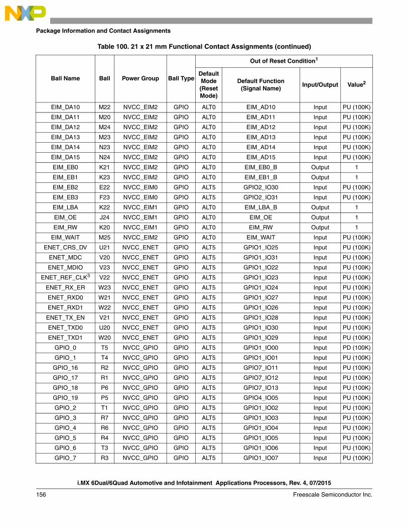
i.MX 6Dual/6Quad Automotive and Infotainment Applications Processors, Rev. 4, 07/2015
156 Freescale Semiconductor Inc.
Package Information and Contact Assignments
EIM_DA10 M22 NVCC_EIM2 GPIO ALT0 EIM_AD10 Input PU (100K)
EIM_DA11 M20 NVCC_EIM2 GPIO ALT0 EIM_AD11 Input PU (100K)
EIM_DA12 M24 NVCC_EIM2 GPIO ALT0 EIM_AD12 Input PU (100K)
EIM_DA13 M23 NVCC_EIM2 GPIO ALT0 EIM_AD13 Input PU (100K)
EIM_DA14 N23 NVCC_EIM2 GPIO ALT0 EIM_AD14 Input PU (100K)
EIM_DA15 N24 NVCC_EIM2 GPIO ALT0 EIM_AD15 Input PU (100K)
EIM_EB0 K21 NVCC_EIM2 GPIO ALT0 EIM_EB0_B Output 1
EIM_EB1 K23 NVCC_EIM2 GPIO ALT0 EIM_EB1_B Output 1
EIM_EB2 E22 NVCC_EIM0 GPIO ALT5 GPIO2_IO30 Input PU (100K)
EIM_EB3 F23 NVCC_EIM0 GPIO ALT5 GPIO2_IO31 Input PU (100K)
EIM_LBA K22 NVCC_EIM1 GPIO ALT0 EIM_LBA_B Output 1
EIM_OE J24 NVCC_EIM1 GPIO ALT0 EIM_OE Output 1
EIM_RW K20 NVCC_EIM1 GPIO ALT0 EIM_RW Output 1
EIM_WAIT M25 NVCC_EIM2 GPIO ALT0 EIM_WAIT Input PU (100K)
ENET_CRS_DV U21 NVCC_ENET GPIO ALT5 GPIO1_IO25 Input PU (100K)
ENET_MDC V20 NVCC_ENET GPIO ALT5 GPIO1_IO31 Input PU (100K)
ENET_MDIO V23 NVCC_ENET GPIO ALT5 GPIO1_IO22 Input PU (100K)
ENET_REF_CLK3 V22 NVCC_ENET GPIO ALT5 GPIO1_IO23 Input PU (100K)
ENET_RX_ER W23 NVCC_ENET GPIO ALT5 GPIO1_IO24 Input PU (100K)
ENET_RXD0 W21 NVCC_ENET GPIO ALT5 GPIO1_IO27 Input PU (100K)
ENET_RXD1 W22 NVCC_ENET GPIO ALT5 GPIO1_IO26 Input PU (100K)
ENET_TX_EN V21 NVCC_ENET GPIO ALT5 GPIO1_IO28 Input PU (100K)
ENET_TXD0 U20 NVCC_ENET GPIO ALT5 GPIO1_IO30 Input PU (100K)
ENET_TXD1 W20 NVCC_ENET GPIO ALT5 GPIO1_IO29 Input PU (100K)
GPIO_0 T5 NVCC_GPIO GPIO ALT5 GPIO1_IO00 Input PD (100K)
GPIO_1 T4 NVCC_GPIO GPIO ALT5 GPIO1_IO01 Input PU (100K)
GPIO_16 R2 NVCC_GPIO GPIO ALT5 GPIO7_IO11 Input PU (100K)
GPIO_17 R1 NVCC_GPIO GPIO ALT5 GPIO7_IO12 Input PU (100K)
GPIO_18 P6 NVCC_GPIO GPIO ALT5 GPIO7_IO13 Input PU (100K)
GPIO_19 P5 NVCC_GPIO GPIO ALT5 GPIO4_IO05 Input PU (100K)
GPIO_2 T1 NVCC_GPIO GPIO ALT5 GPIO1_IO02 Input PU (100K)
GPIO_3 R7 NVCC_GPIO GPIO ALT5 GPIO1_IO03 Input PU (100K)
GPIO_4 R6 NVCC_GPIO GPIO ALT5 GPIO1_IO04 Input PU (100K)
GPIO_5 R4 NVCC_GPIO GPIO ALT5 GPIO1_IO05 Input PU (100K)
GPIO_6 T3 NVCC_GPIO GPIO ALT5 GPIO1_IO06 Input PU (100K)
GPIO_7 R3 NVCC_GPIO GPIO ALT5 GPIO1_IO07 Input PU (100K)
Table 100. 21 x 21 mm Functional Contact Assignments (continued)
Ball Name Ball Power Group Ball Type
Out of Reset Condition1
Default Mode (Reset Mode)
Default Function(Signal Name)
Input/Output Value2
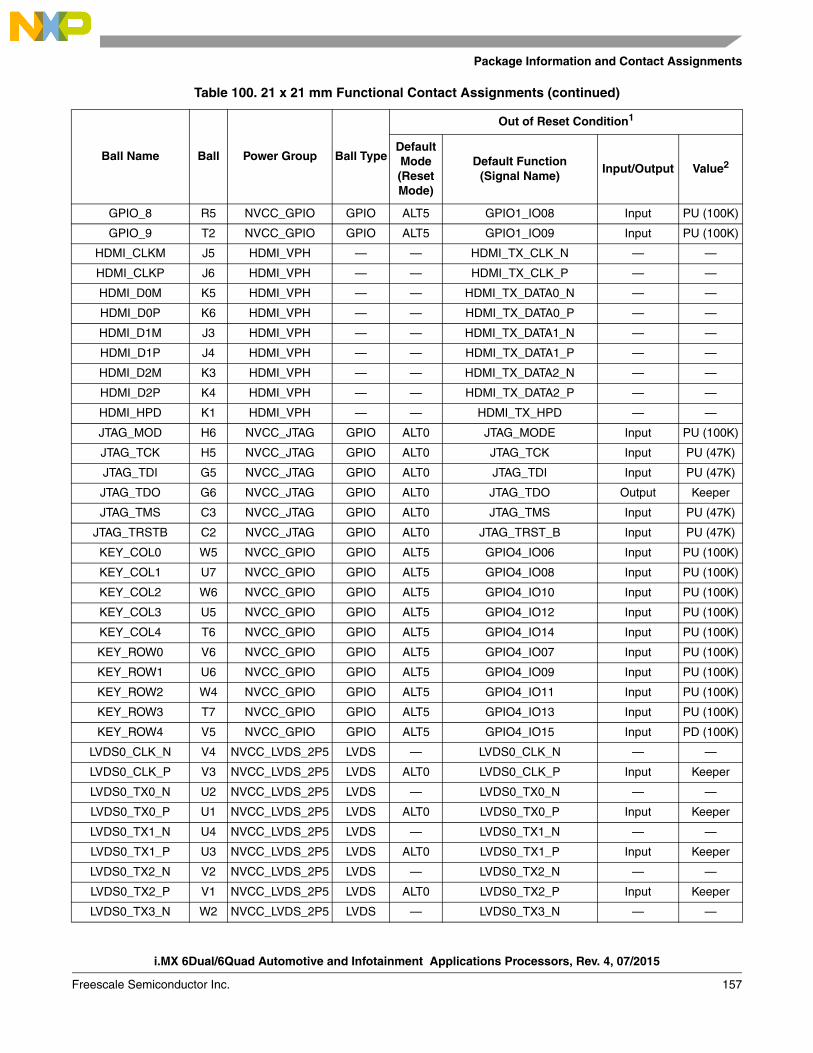
Package Information and Contact Assignments
i.MX 6Dual/6Quad Automotive and Infotainment Applications Processors, Rev. 4, 07/2015
Freescale Semiconductor Inc. 157
GPIO_8 R5 NVCC_GPIO GPIO ALT5 GPIO1_IO08 Input PU (100K)
GPIO_9 T2 NVCC_GPIO GPIO ALT5 GPIO1_IO09 Input PU (100K)
HDMI_CLKM J5 HDMI_VPH — — HDMI_TX_CLK_N — —
HDMI_CLKP J6 HDMI_VPH — — HDMI_TX_CLK_P — —
HDMI_D0M K5 HDMI_VPH — — HDMI_TX_DATA0_N — —
HDMI_D0P K6 HDMI_VPH — — HDMI_TX_DATA0_P — —
HDMI_D1M J3 HDMI_VPH — — HDMI_TX_DATA1_N — —
HDMI_D1P J4 HDMI_VPH — — HDMI_TX_DATA1_P — —
HDMI_D2M K3 HDMI_VPH — — HDMI_TX_DATA2_N — —
HDMI_D2P K4 HDMI_VPH — — HDMI_TX_DATA2_P — —
HDMI_HPD K1 HDMI_VPH — — HDMI_TX_HPD — —
JTAG_MOD H6 NVCC_JTAG GPIO ALT0 JTAG_MODE Input PU (100K)
JTAG_TCK H5 NVCC_JTAG GPIO ALT0 JTAG_TCK Input PU (47K)
JTAG_TDI G5 NVCC_JTAG GPIO ALT0 JTAG_TDI Input PU (47K)
JTAG_TDO G6 NVCC_JTAG GPIO ALT0 JTAG_TDO Output Keeper
JTAG_TMS C3 NVCC_JTAG GPIO ALT0 JTAG_TMS Input PU (47K)
JTAG_TRSTB C2 NVCC_JTAG GPIO ALT0 JTAG_TRST_B Input PU (47K)
KEY_COL0 W5 NVCC_GPIO GPIO ALT5 GPIO4_IO06 Input PU (100K)
KEY_COL1 U7 NVCC_GPIO GPIO ALT5 GPIO4_IO08 Input PU (100K)
KEY_COL2 W6 NVCC_GPIO GPIO ALT5 GPIO4_IO10 Input PU (100K)
KEY_COL3 U5 NVCC_GPIO GPIO ALT5 GPIO4_IO12 Input PU (100K)
KEY_COL4 T6 NVCC_GPIO GPIO ALT5 GPIO4_IO14 Input PU (100K)
KEY_ROW0 V6 NVCC_GPIO GPIO ALT5 GPIO4_IO07 Input PU (100K)
KEY_ROW1 U6 NVCC_GPIO GPIO ALT5 GPIO4_IO09 Input PU (100K)
KEY_ROW2 W4 NVCC_GPIO GPIO ALT5 GPIO4_IO11 Input PU (100K)
KEY_ROW3 T7 NVCC_GPIO GPIO ALT5 GPIO4_IO13 Input PU (100K)
KEY_ROW4 V5 NVCC_GPIO GPIO ALT5 GPIO4_IO15 Input PD (100K)
LVDS0_CLK_N V4 NVCC_LVDS_2P5 LVDS — LVDS0_CLK_N — —
LVDS0_CLK_P V3 NVCC_LVDS_2P5 LVDS ALT0 LVDS0_CLK_P Input Keeper
LVDS0_TX0_N U2 NVCC_LVDS_2P5 LVDS — LVDS0_TX0_N — —
LVDS0_TX0_P U1 NVCC_LVDS_2P5 LVDS ALT0 LVDS0_TX0_P Input Keeper
LVDS0_TX1_N U4 NVCC_LVDS_2P5 LVDS — LVDS0_TX1_N — —
LVDS0_TX1_P U3 NVCC_LVDS_2P5 LVDS ALT0 LVDS0_TX1_P Input Keeper
LVDS0_TX2_N V2 NVCC_LVDS_2P5 LVDS — LVDS0_TX2_N — —
LVDS0_TX2_P V1 NVCC_LVDS_2P5 LVDS ALT0 LVDS0_TX2_P Input Keeper
LVDS0_TX3_N W2 NVCC_LVDS_2P5 LVDS — LVDS0_TX3_N — —
Table 100. 21 x 21 mm Functional Contact Assignments (continued)
Ball Name Ball Power Group Ball Type
Out of Reset Condition1
Default Mode (Reset Mode)
Default Function(Signal Name)
Input/Output Value2
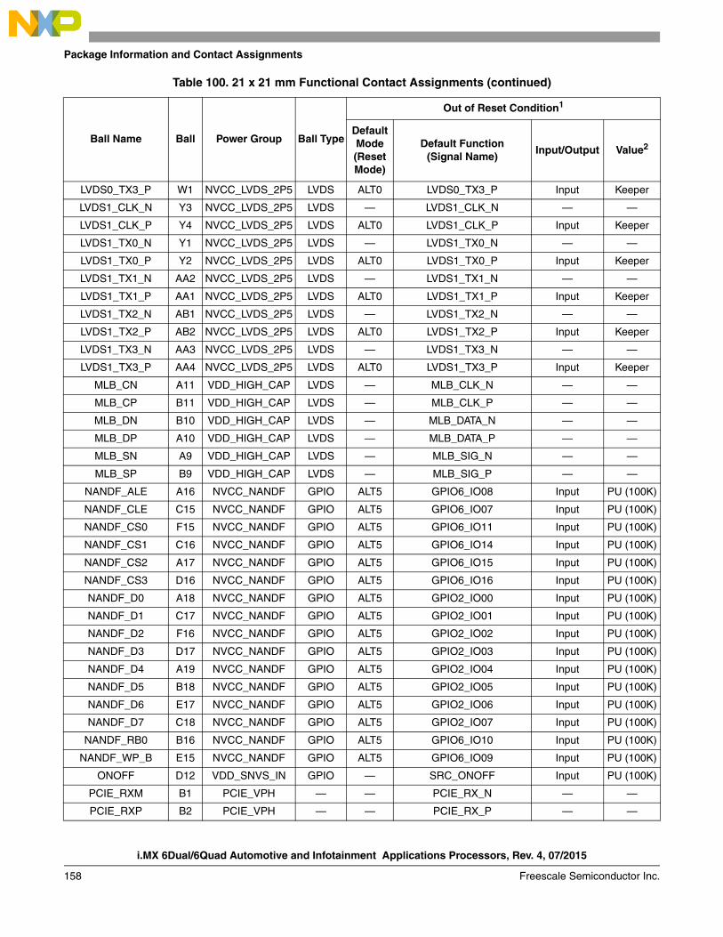
i.MX 6Dual/6Quad Automotive and Infotainment Applications Processors, Rev. 4, 07/2015
158 Freescale Semiconductor Inc.
Package Information and Contact Assignments
LVDS0_TX3_P W1 NVCC_LVDS_2P5 LVDS ALT0 LVDS0_TX3_P Input Keeper
LVDS1_CLK_N Y3 NVCC_LVDS_2P5 LVDS — LVDS1_CLK_N — —
LVDS1_CLK_P Y4 NVCC_LVDS_2P5 LVDS ALT0 LVDS1_CLK_P Input Keeper
LVDS1_TX0_N Y1 NVCC_LVDS_2P5 LVDS — LVDS1_TX0_N — —
LVDS1_TX0_P Y2 NVCC_LVDS_2P5 LVDS ALT0 LVDS1_TX0_P Input Keeper
LVDS1_TX1_N AA2 NVCC_LVDS_2P5 LVDS — LVDS1_TX1_N — —
LVDS1_TX1_P AA1 NVCC_LVDS_2P5 LVDS ALT0 LVDS1_TX1_P Input Keeper
LVDS1_TX2_N AB1 NVCC_LVDS_2P5 LVDS — LVDS1_TX2_N — —
LVDS1_TX2_P AB2 NVCC_LVDS_2P5 LVDS ALT0 LVDS1_TX2_P Input Keeper
LVDS1_TX3_N AA3 NVCC_LVDS_2P5 LVDS — LVDS1_TX3_N — —
LVDS1_TX3_P AA4 NVCC_LVDS_2P5 LVDS ALT0 LVDS1_TX3_P Input Keeper
MLB_CN A11 VDD_HIGH_CAP LVDS — MLB_CLK_N — —
MLB_CP B11 VDD_HIGH_CAP LVDS — MLB_CLK_P — —
MLB_DN B10 VDD_HIGH_CAP LVDS — MLB_DATA_N — —
MLB_DP A10 VDD_HIGH_CAP LVDS — MLB_DATA_P — —
MLB_SN A9 VDD_HIGH_CAP LVDS — MLB_SIG_N — —
MLB_SP B9 VDD_HIGH_CAP LVDS — MLB_SIG_P — —
NANDF_ALE A16 NVCC_NANDF GPIO ALT5 GPIO6_IO08 Input PU (100K)
NANDF_CLE C15 NVCC_NANDF GPIO ALT5 GPIO6_IO07 Input PU (100K)
NANDF_CS0 F15 NVCC_NANDF GPIO ALT5 GPIO6_IO11 Input PU (100K)
NANDF_CS1 C16 NVCC_NANDF GPIO ALT5 GPIO6_IO14 Input PU (100K)
NANDF_CS2 A17 NVCC_NANDF GPIO ALT5 GPIO6_IO15 Input PU (100K)
NANDF_CS3 D16 NVCC_NANDF GPIO ALT5 GPIO6_IO16 Input PU (100K)
NANDF_D0 A18 NVCC_NANDF GPIO ALT5 GPIO2_IO00 Input PU (100K)
NANDF_D1 C17 NVCC_NANDF GPIO ALT5 GPIO2_IO01 Input PU (100K)
NANDF_D2 F16 NVCC_NANDF GPIO ALT5 GPIO2_IO02 Input PU (100K)
NANDF_D3 D17 NVCC_NANDF GPIO ALT5 GPIO2_IO03 Input PU (100K)
NANDF_D4 A19 NVCC_NANDF GPIO ALT5 GPIO2_IO04 Input PU (100K)
NANDF_D5 B18 NVCC_NANDF GPIO ALT5 GPIO2_IO05 Input PU (100K)
NANDF_D6 E17 NVCC_NANDF GPIO ALT5 GPIO2_IO06 Input PU (100K)
NANDF_D7 C18 NVCC_NANDF GPIO ALT5 GPIO2_IO07 Input PU (100K)
NANDF_RB0 B16 NVCC_NANDF GPIO ALT5 GPIO6_IO10 Input PU (100K)
NANDF_WP_B E15 NVCC_NANDF GPIO ALT5 GPIO6_IO09 Input PU (100K)
ONOFF D12 VDD_SNVS_IN GPIO — SRC_ONOFF Input PU (100K)
PCIE_RXM B1 PCIE_VPH — — PCIE_RX_N — —
PCIE_RXP B2 PCIE_VPH — — PCIE_RX_P — —
Table 100. 21 x 21 mm Functional Contact Assignments (continued)
Ball Name Ball Power Group Ball Type
Out of Reset Condition1
Default Mode (Reset Mode)
Default Function(Signal Name)
Input/Output Value2
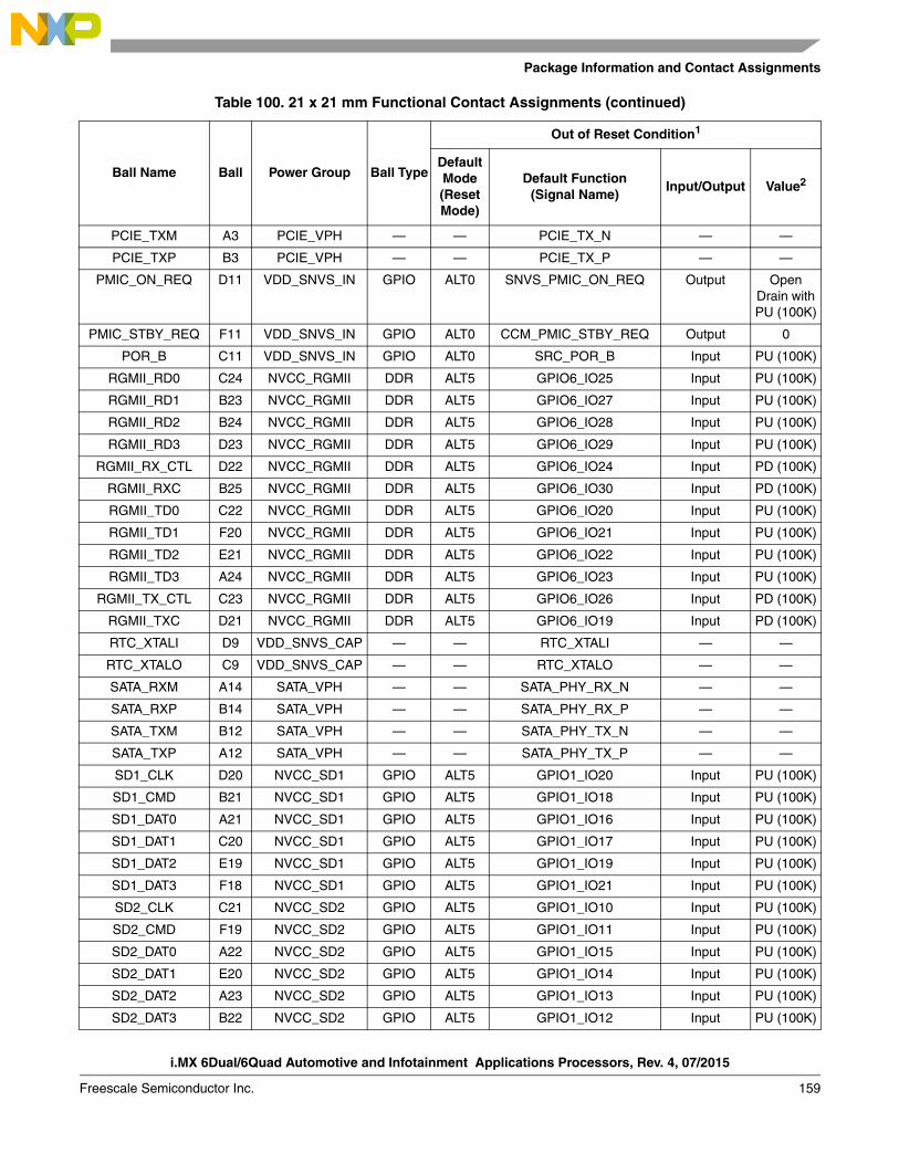
Package Information and Contact Assignments
i.MX 6Dual/6Quad Automotive and Infotainment Applications Processors, Rev. 4, 07/2015
Freescale Semiconductor Inc. 159
PCIE_TXM A3 PCIE_VPH — — PCIE_TX_N — —
PCIE_TXP B3 PCIE_VPH — — PCIE_TX_P — —
PMIC_ON_REQ D11 VDD_SNVS_IN GPIO ALT0 SNVS_PMIC_ON_REQ Output Open Drain with PU (100K)
PMIC_STBY_REQ F11 VDD_SNVS_IN GPIO ALT0 CCM_PMIC_STBY_REQ Output 0
POR_B C11 VDD_SNVS_IN GPIO ALT0 SRC_POR_B Input PU (100K)
RGMII_RD0 C24 NVCC_RGMII DDR ALT5 GPIO6_IO25 Input PU (100K)
RGMII_RD1 B23 NVCC_RGMII DDR ALT5 GPIO6_IO27 Input PU (100K)
RGMII_RD2 B24 NVCC_RGMII DDR ALT5 GPIO6_IO28 Input PU (100K)
RGMII_RD3 D23 NVCC_RGMII DDR ALT5 GPIO6_IO29 Input PU (100K)
RGMII_RX_CTL D22 NVCC_RGMII DDR ALT5 GPIO6_IO24 Input PD (100K)
RGMII_RXC B25 NVCC_RGMII DDR ALT5 GPIO6_IO30 Input PD (100K)
RGMII_TD0 C22 NVCC_RGMII DDR ALT5 GPIO6_IO20 Input PU (100K)
RGMII_TD1 F20 NVCC_RGMII DDR ALT5 GPIO6_IO21 Input PU (100K)
RGMII_TD2 E21 NVCC_RGMII DDR ALT5 GPIO6_IO22 Input PU (100K)
RGMII_TD3 A24 NVCC_RGMII DDR ALT5 GPIO6_IO23 Input PU (100K)
RGMII_TX_CTL C23 NVCC_RGMII DDR ALT5 GPIO6_IO26 Input PD (100K)
RGMII_TXC D21 NVCC_RGMII DDR ALT5 GPIO6_IO19 Input PD (100K)
RTC_XTALI D9 VDD_SNVS_CAP — — RTC_XTALI — —
RTC_XTALO C9 VDD_SNVS_CAP — — RTC_XTALO — —
SATA_RXM A14 SATA_VPH — — SATA_PHY_RX_N — —
SATA_RXP B14 SATA_VPH — — SATA_PHY_RX_P — —
SATA_TXM B12 SATA_VPH — — SATA_PHY_TX_N — —
SATA_TXP A12 SATA_VPH — — SATA_PHY_TX_P — —
SD1_CLK D20 NVCC_SD1 GPIO ALT5 GPIO1_IO20 Input PU (100K)
SD1_CMD B21 NVCC_SD1 GPIO ALT5 GPIO1_IO18 Input PU (100K)
SD1_DAT0 A21 NVCC_SD1 GPIO ALT5 GPIO1_IO16 Input PU (100K)
SD1_DAT1 C20 NVCC_SD1 GPIO ALT5 GPIO1_IO17 Input PU (100K)
SD1_DAT2 E19 NVCC_SD1 GPIO ALT5 GPIO1_IO19 Input PU (100K)
SD1_DAT3 F18 NVCC_SD1 GPIO ALT5 GPIO1_IO21 Input PU (100K)
SD2_CLK C21 NVCC_SD2 GPIO ALT5 GPIO1_IO10 Input PU (100K)
SD2_CMD F19 NVCC_SD2 GPIO ALT5 GPIO1_IO11 Input PU (100K)
SD2_DAT0 A22 NVCC_SD2 GPIO ALT5 GPIO1_IO15 Input PU (100K)
SD2_DAT1 E20 NVCC_SD2 GPIO ALT5 GPIO1_IO14 Input PU (100K)
SD2_DAT2 A23 NVCC_SD2 GPIO ALT5 GPIO1_IO13 Input PU (100K)
SD2_DAT3 B22 NVCC_SD2 GPIO ALT5 GPIO1_IO12 Input PU (100K)
Table 100. 21 x 21 mm Functional Contact Assignments (continued)
Ball Name Ball Power Group Ball Type
Out of Reset Condition1
Default Mode (Reset Mode)
Default Function(Signal Name)
Input/Output Value2
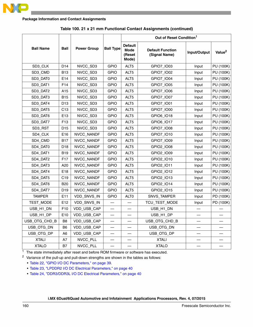
i.MX 6Dual/6Quad Automotive and Infotainment Applications Processors, Rev. 4, 07/2015
160 Freescale Semiconductor Inc.
Package Information and Contact Assignments
SD3_CLK D14 NVCC_SD3 GPIO ALT5 GPIO7_IO03 Input PU (100K)
SD3_CMD B13 NVCC_SD3 GPIO ALT5 GPIO7_IO02 Input PU (100K)
SD3_DAT0 E14 NVCC_SD3 GPIO ALT5 GPIO7_IO04 Input PU (100K)
SD3_DAT1 F14 NVCC_SD3 GPIO ALT5 GPIO7_IO05 Input PU (100K)
SD3_DAT2 A15 NVCC_SD3 GPIO ALT5 GPIO7_IO06 Input PU (100K)
SD3_DAT3 B15 NVCC_SD3 GPIO ALT5 GPIO7_IO07 Input PU (100K)
SD3_DAT4 D13 NVCC_SD3 GPIO ALT5 GPIO7_IO01 Input PU (100K)
SD3_DAT5 C13 NVCC_SD3 GPIO ALT5 GPIO7_IO00 Input PU (100K)
SD3_DAT6 E13 NVCC_SD3 GPIO ALT5 GPIO6_IO18 Input PU (100K)
SD3_DAT7 F13 NVCC_SD3 GPIO ALT5 GPIO6_IO17 Input PU (100K)
SD3_RST D15 NVCC_SD3 GPIO ALT5 GPIO7_IO08 Input PU (100K)
SD4_CLK E16 NVCC_NANDF GPIO ALT5 GPIO7_IO10 Input PU (100K)
SD4_CMD B17 NVCC_NANDF GPIO ALT5 GPIO7_IO09 Input PU (100K)
SD4_DAT0 D18 NVCC_NANDF GPIO ALT5 GPIO2_IO08 Input PU (100K)
SD4_DAT1 B19 NVCC_NANDF GPIO ALT5 GPIO2_IO09 Input PU (100K)
SD4_DAT2 F17 NVCC_NANDF GPIO ALT5 GPIO2_IO10 Input PU (100K)
SD4_DAT3 A20 NVCC_NANDF GPIO ALT5 GPIO2_IO11 Input PU (100K)
SD4_DAT4 E18 NVCC_NANDF GPIO ALT5 GPIO2_IO12 Input PU (100K)
SD4_DAT5 C19 NVCC_NANDF GPIO ALT5 GPIO2_IO13 Input PU (100K)
SD4_DAT6 B20 NVCC_NANDF GPIO ALT5 GPIO2_IO14 Input PU (100K)
SD4_DAT7 D19 NVCC_NANDF GPIO ALT5 GPIO2_IO15 Input PU (100K)
TAMPER E11 VDD_SNVS_IN GPIO ALT0 SNVS_TAMPER Input PD (100K)
TEST_MODE E12 VDD_SNVS_IN — — TCU_TEST_MODE Input PD (100K)
USB_H1_DN F10 VDD_USB_CAP — — USB_H1_DN — —
USB_H1_DP E10 VDD_USB_CAP — — USB_H1_DP — —
USB_OTG_CHD_B B8 VDD_USB_CAP — — USB_OTG_CHD_B — —
USB_OTG_DN B6 VDD_USB_CAP — — USB_OTG_DN — —
USB_OTG_DP A6 VDD_USB_CAP — — USB_OTG_DP — —
XTALI A7 NVCC_PLL — — XTALI — —
XTALO B7 NVCC_PLL — — XTALO — —1 The state immediately after reset and before ROM firmware or software has executed.2 Variance of the pull-up and pull-down strengths are shown in the tables as follows:
• Table 22, "GPIO I/O DC Parameters," on page 39.
• Table 23, "LPDDR2 I/O DC Electrical Parameters," on page 40
• Table 24, "DDR3/DDR3L I/O DC Electrical Parameters," on page 40
Table 100. 21 x 21 mm Functional Contact Assignments (continued)
Ball Name Ball Power Group Ball Type
Out of Reset Condition1
Default Mode (Reset Mode)
Default Function(Signal Name)
Input/Output Value2
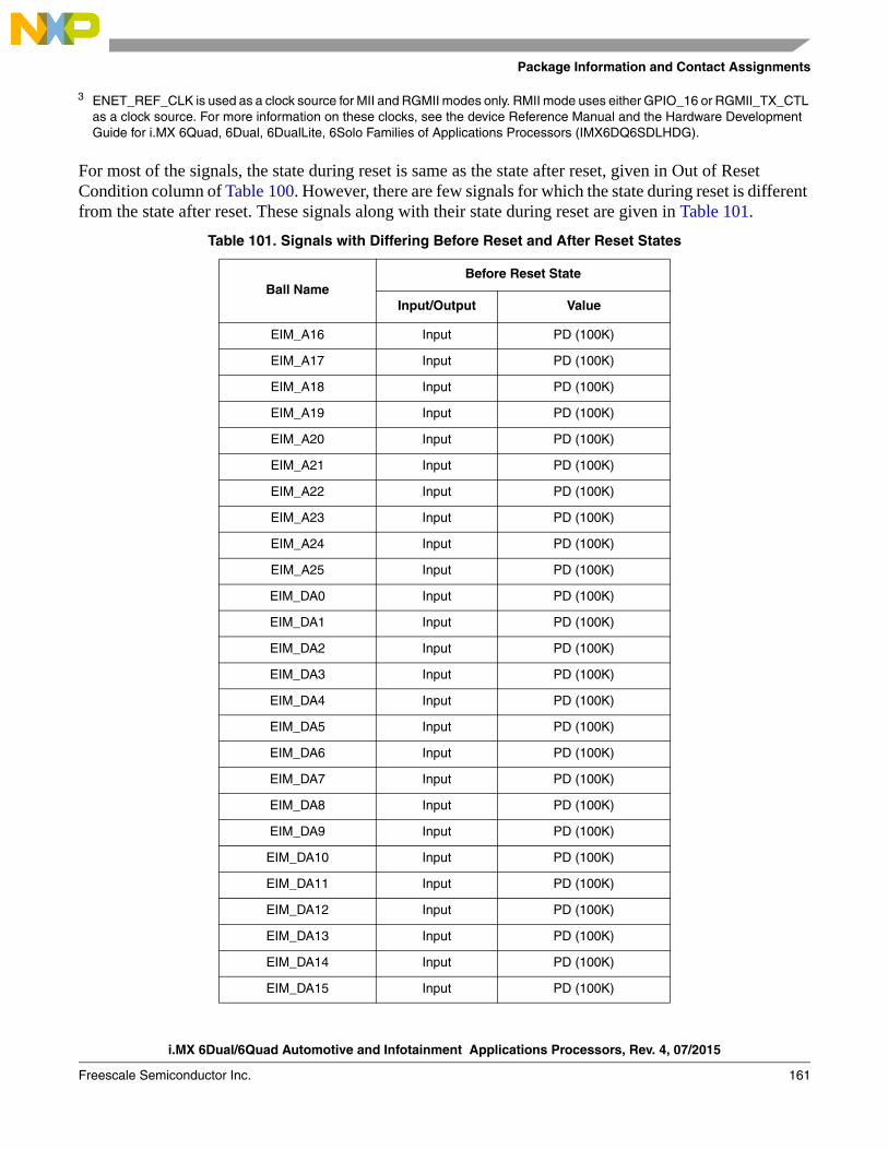
Package Information and Contact Assignments
i.MX 6Dual/6Quad Automotive and Infotainment Applications Processors, Rev. 4, 07/2015
Freescale Semiconductor Inc. 161
For most of the signals, the state during reset is same as the state after reset, given in Out of Reset Condition column of Table 100. However, there are few signals for which the state during reset is different from the state after reset. These signals along with their state during reset are given in Table 101.
3 ENET_REF_CLK is used as a clock source for MII and RGMII modes only. RMII mode uses either GPIO_16 or RGMII_TX_CTL as a clock source. For more information on these clocks, see the device Reference Manual and the Hardware Development Guide for i.MX 6Quad, 6Dual, 6DualLite, 6Solo Families of Applications Processors (IMX6DQ6SDLHDG).
Table 101. Signals with Differing Before Reset and After Reset States
Ball NameBefore Reset State
Input/Output Value
EIM_A16 Input PD (100K)
EIM_A17 Input PD (100K)
EIM_A18 Input PD (100K)
EIM_A19 Input PD (100K)
EIM_A20 Input PD (100K)
EIM_A21 Input PD (100K)
EIM_A22 Input PD (100K)
EIM_A23 Input PD (100K)
EIM_A24 Input PD (100K)
EIM_A25 Input PD (100K)
EIM_DA0 Input PD (100K)
EIM_DA1 Input PD (100K)
EIM_DA2 Input PD (100K)
EIM_DA3 Input PD (100K)
EIM_DA4 Input PD (100K)
EIM_DA5 Input PD (100K)
EIM_DA6 Input PD (100K)
EIM_DA7 Input PD (100K)
EIM_DA8 Input PD (100K)
EIM_DA9 Input PD (100K)
EIM_DA10 Input PD (100K)
EIM_DA11 Input PD (100K)
EIM_DA12 Input PD (100K)
EIM_DA13 Input PD (100K)
EIM_DA14 Input PD (100K)
EIM_DA15 Input PD (100K)
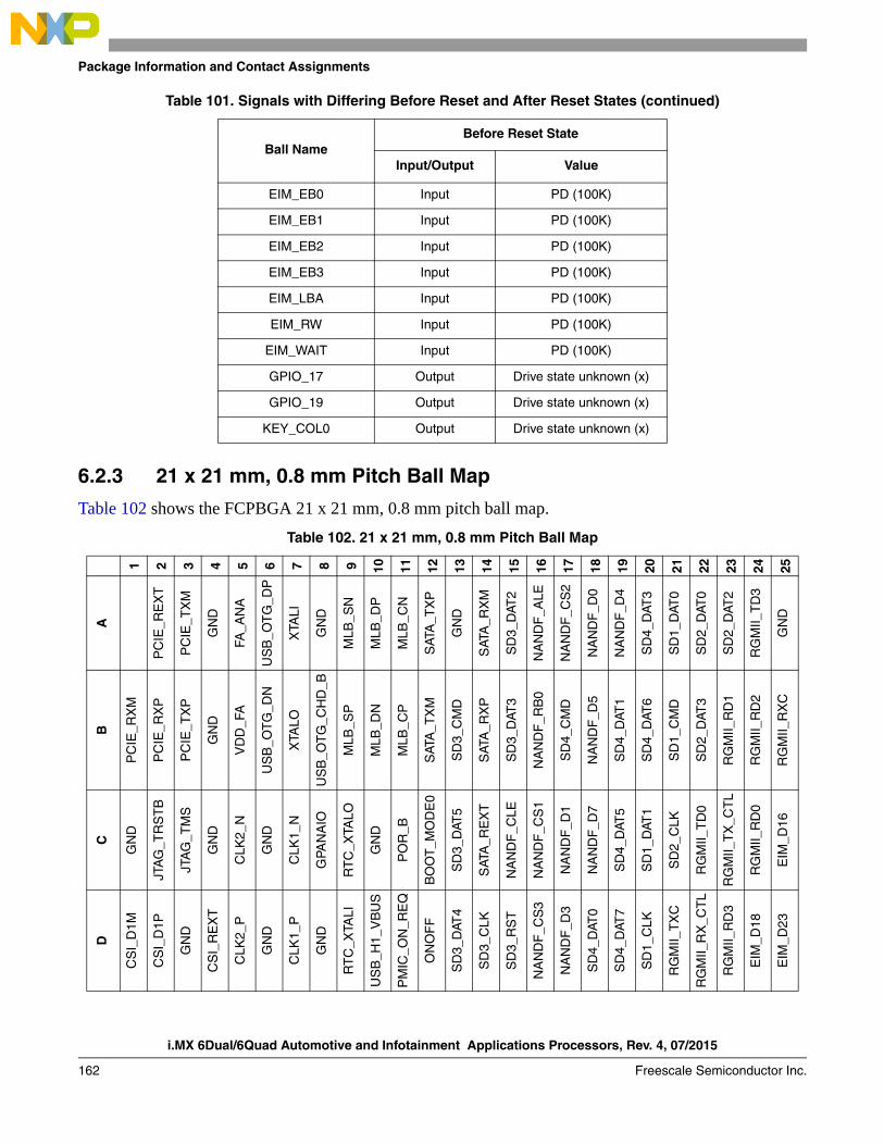
i.MX 6Dual/6Quad Automotive and Infotainment Applications Processors, Rev. 4, 07/2015
162 Freescale Semiconductor Inc.
Package Information and Contact Assignments
6.2.3 21 x 21 mm, 0.8 mm Pitch Ball Map
Table 102 shows the FCPBGA 21 x 21 mm, 0.8 mm pitch ball map.
EIM_EB0 Input PD (100K)
EIM_EB1 Input PD (100K)
EIM_EB2 Input PD (100K)
EIM_EB3 Input PD (100K)
EIM_LBA Input PD (100K)
EIM_RW Input PD (100K)
EIM_WAIT Input PD (100K)
GPIO_17 Output Drive state unknown (x)
GPIO_19 Output Drive state unknown (x)
KEY_COL0 Output Drive state unknown (x)
Table 102. 21 x 21 mm, 0.8 mm Pitch Ball Map
1 2 3 4 5 6 7 8 9 10 11 12 13 14 15 16 17 18 19 20 21 22 23 24 25
A
PC
IE_R
EX
T
PC
IE_T
XM
GN
D
FA_A
NA
US
B_O
TG
_DP
XTA
LI
GN
D
MLB
_SN
MLB
_DP
MLB
_CN
SAT
A_T
XP
GN
D
SAT
A_R
XM
SD
3_D
AT2
NA
ND
F_A
LE
NA
ND
F_C
S2
NA
ND
F_D
0
NA
ND
F_D
4
SD
4_D
AT3
SD
1_D
AT0
SD
2_D
AT0
SD
2_D
AT2
RG
MII_
TD
3
GN
D
B
PC
IE_R
XM
PC
IE_R
XP
PC
IE_T
XP
GN
D
VD
D_F
A
US
B_O
TG
_DN
XTA
LO
US
B_O
TG
_CH
D_B
MLB
_SP
MLB
_DN
MLB
_CP
SAT
A_T
XM
SD
3_C
MD
SAT
A_R
XP
SD
3_D
AT3
NA
ND
F_R
B0
SD
4_C
MD
NA
ND
F_D
5
SD
4_D
AT1
SD
4_D
AT6
SD
1_C
MD
SD
2_D
AT3
RG
MII_
RD
1
RG
MII_
RD
2
RG
MII_
RX
C
C
GN
D
JTA
G_T
RS
TB
JTA
G_T
MS
GN
D
CLK
2_N
GN
D
CLK
1_N
GPA
NA
IO
RT
C_X
TALO
GN
D
PO
R_B
BO
OT
_MO
DE
0
SD
3_D
AT5
SAT
A_R
EX
T
NA
ND
F_C
LE
NA
ND
F_C
S1
NA
ND
F_D
1
NA
ND
F_D
7
SD
4_D
AT5
SD
1_D
AT1
SD
2_C
LK
RG
MII_
TD
0
RG
MII_
TX
_CT
L
RG
MII_
RD
0
EIM
_D16
D
CS
I_D
1M
CS
I_D
1P
GN
D
CS
I_R
EX
T
CLK
2_P
GN
D
CLK
1_P
GN
D
RT
C_X
TALI
US
B_H
1_V
BU
S
PM
IC_O
N_R
EQ
ON
OF
F
SD
3_D
AT4
SD
3_C
LK
SD
3_R
ST
NA
ND
F_C
S3
NA
ND
F_D
3
SD
4_D
AT0
SD
4_D
AT7
SD
1_C
LK
RG
MII_
TX
C
RG
MII_
RX
_CT
L
RG
MII_
RD
3
EIM
_D18
EIM
_D23
Table 101. Signals with Differing Before Reset and After Reset States (continued)
Ball NameBefore Reset State
Input/Output Value
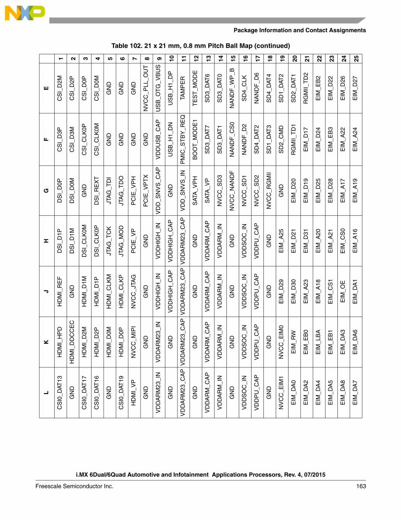
Package Information and Contact Assignments
i.MX 6Dual/6Quad Automotive and Infotainment Applications Processors, Rev. 4, 07/2015
Freescale Semiconductor Inc. 163
E
CS
I_D
2M
CS
I_D
2P
CS
I_D
0P
CS
I_D
0M
GN
D
GN
D
GN
D
NV
CC
_PLL
_OU
T
US
B_O
TG
_VB
US
US
B_H
1_D
P
TAM
PE
R
TE
ST
_MO
DE
SD
3_D
AT6
SD
3_D
AT0
NA
ND
F_W
P_B
SD
4_C
LK
NA
ND
F_D
6
SD
4_D
AT4
SD
1_D
AT2
SD
2_D
AT1
RG
MII_
TD
2
EIM
_EB
2
EIM
_D22
EIM
_D26
EIM
_D27
F
CS
I_D
3P
CS
I_D
3M
CS
I_C
LK0P
CS
I_C
LK0M
GN
D
GN
D
GN
D
GN
D
VD
DU
SB
_CA
P
US
B_H
1_D
N
PM
IC_S
TB
Y_R
EQ
BO
OT
_MO
DE
1
SD
3_D
AT7
SD
3_D
AT1
NA
ND
F_C
S0
NA
ND
F_D
2
SD
4_D
AT2
SD
1_D
AT3
SD
2_C
MD
RG
MII_
TD
1
EIM
_D17
EIM
_D24
EIM
_EB
3
EIM
_A22
EIM
_A24
G
DS
I_D
0P
DS
I_D
0M
GN
D
DS
I_R
EX
T
JTA
G_T
DI
JTA
G_T
DO
PC
IE_V
PH
PC
IE_V
PT
X
VD
D_S
NV
S_C
AP
GN
D
VD
D_S
NV
S_I
N
SAT
A_V
PH
SAT
A_V
P
NV
CC
_SD
3
NV
CC
_NA
ND
F
NV
CC
_SD
1
NV
CC
_SD
2
NV
CC
_RG
MII
GN
D
EIM
_D20
EIM
_D19
EIM
_D25
EIM
_D28
EIM
_A17
EIM
_A19
H
DS
I_D
1P
DS
I_D
1M
DS
I_C
LK0M
DS
I_C
LK0P
JTA
G_T
CK
JTA
G_M
OD
PC
IE_V
P
GN
D
VD
DH
IGH
_IN
VD
DH
IGH
_CA
P
VD
DA
RM
23_C
AP
GN
D
VD
DA
RM
_CA
P
VD
DA
RM
_IN
GN
D
VD
DS
OC
_IN
VD
DP
U_C
AP
GN
D
EIM
_A25
EIM
_D21
EIM
_D31
EIM
_A20
EIM
_A21
EIM
_CS
0
EIM
_A16
J
HD
MI_
RE
F
GN
D
HD
MI_
D1M
HD
MI_
D1P
HD
MI_
CLK
M
HD
MI_
CLK
P
NV
CC
_JTA
G
GN
D
VD
DH
IGH
_IN
VD
DH
IGH
_CA
P
VD
DA
RM
23_C
AP
GN
D
VD
DA
RM
_CA
P
VD
DA
RM
_IN
GN
D
VD
DS
OC
_IN
VD
DP
U_C
AP
GN
D
EIM
_D29
EIM
_D30
EIM
_A23
EIM
_A18
EIM
_CS
1
EIM
_OE
EIM
_DA
1
K
HD
MI_
HP
D
HD
MI_
DD
CC
EC
HD
MI_
D2M
HD
MI_
D2P
HD
MI_
D0M
HD
MI_
D0P
NV
CC
_MIP
I
GN
D
VD
DA
RM
23_I
N
GN
D
VD
DA
RM
23_C
AP
GN
D
VD
DA
RM
_CA
P
VD
DA
RM
_IN
GN
D
VD
DS
OC
_IN
VD
DP
U_C
AP
GN
D
NV
CC
_EIM
0
EIM
_RW
EIM
_EB
0
EIM
_LB
A
EIM
_EB
1
EIM
_DA
3
EIM
_DA
6
L
CS
I0_D
AT13
GN
D
CS
I0_D
AT17
CS
I0_D
AT16
GN
D
CS
I0_D
AT19
HD
MI_
VP
GN
D
VD
DA
RM
23_I
N
GN
D
VD
DA
RM
23_C
AP
GN
D
VD
DA
RM
_CA
P
VD
DA
RM
_IN
GN
D
VD
DS
OC
_IN
VD
DP
U_C
AP
GN
D
NV
CC
_EIM
1
EIM
_DA
0
EIM
_DA
2
EIM
_DA
4
EIM
_DA
5
EIM
_DA
8
EIM
_DA
7
Table 102. 21 x 21 mm, 0.8 mm Pitch Ball Map (continued)
1 2 3 4 5 6 7 8 9 10 11 12 13 14 15 16 17 18 19 20 21 22 23 24 25
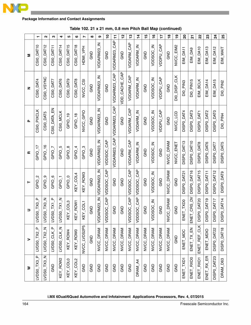
i.MX 6Dual/6Quad Automotive and Infotainment Applications Processors, Rev. 4, 07/2015
164 Freescale Semiconductor Inc.
Package Information and Contact Assignments
M
CS
I0_D
AT10
CS
I0_D
AT12
CS
I0_D
AT11
CS
I0_D
AT14
CS
I0_D
AT15
CS
I0_D
AT18
HD
MI_
VP
H
GN
D
VD
DA
RM
23_I
N
GN
D
VD
DA
RM
23_C
AP
GN
D
VD
DA
RM
_CA
P
VD
DA
RM
_IN
GN
D
VD
DS
OC
_IN
VD
DP
U_C
AP
GN
D
NV
CC
_EIM
2
EIM
_DA
11
EIM
_DA
9
EIM
_DA
10
EIM
_DA
13
EIM
_DA
12
EIM
_WA
IT
N
CS
I0_D
AT4
CS
I0_V
SY
NC
CS
I0_D
AT7
CS
I0_D
AT6
CS
I0_D
AT9
CS
I0_D
AT8
NV
CC
_CS
I
GN
D
VD
DA
RM
23_I
N
GN
D
VD
DA
RM
23_C
AP
VD
D_C
AC
HE
_CA
P
VD
DA
RM
_CA
P
VD
DA
RM
_IN
GN
D
VD
DS
OC
_IN
VD
DP
U_C
AP
GN
D
DI0
_DIS
P_C
LK
DI0
_PIN
3
DI0
_PIN
15
EIM
_BC
LK
EIM
_DA
14
EIM
_DA
15
DI0
_PIN
2
P
CS
I0_P
IXC
LK
CS
I0_D
AT5
CS
I0_D
ATA
_EN
CS
I0_M
CLK
GP
IO_1
9
GP
IO_1
8
NV
CC
_GP
IO
GN
D
VD
DA
RM
23_I
N
GN
D
VD
DA
RM
23_C
AP
GN
D
VD
DA
RM
_CA
P
VD
DA
RM
_IN
GN
D
VD
DS
OC
_IN
VD
DP
U_C
AP
GN
D
NV
CC
_LC
D
DIS
P0_
DAT
4
DIS
P0_
DAT
3
DIS
P0_
DAT
1
DIS
P0_
DAT
2
DIS
P0_
DAT
0
DI0
_PIN
4
R
GP
IO_1
7
GP
IO_1
6
GP
IO_7
GP
IO_5
GP
IO_8
GP
IO_4
GP
IO_3
GN
D
VD
DA
RM
23_I
N
VD
DS
OC
_CA
P
VD
DA
RM
23_C
AP
GN
D
VD
DA
RM
_CA
P
VD
DA
RM
_IN
GN
D
VD
DS
OC
_IN
GN
D
NV
CC
_DR
AM
NV
CC
_EN
ET
DIS
P0_
DAT
13
DIS
P0_
DAT
10
DIS
P0_
DAT
8
DIS
P0_
DAT
6
DIS
P0_
DAT
7
DIS
P0_
DAT
5
T
GP
IO_2
GP
IO_9
GP
IO_6
GP
IO_1
GP
IO_0
KE
Y_C
OL4
KE
Y_R
OW
3
GN
D
VD
DA
RM
23_I
N
VD
DS
OC
_CA
P
GN
D
GN
D
VD
DS
OC
_CA
P
VD
DS
OC
_CA
P
GN
D
VD
DS
OC
_IN
GN
D
NV
CC
_DR
AM
GN
D
DIS
P0_
DAT
21
DIS
P0_
DAT
16
DIS
P0_
DAT
15
DIS
P0_
DAT
11
DIS
P0_
DAT
12
DIS
P0_
DAT
9
U
LVD
S0_
TX
0_P
LVD
S0_
TX
0_N
LVD
S0_
TX
1_P
LVD
S0_
TX
1_N
KE
Y_C
OL3
KE
Y_R
OW
1
KE
Y_C
OL1
GN
D
VD
DA
RM
23_I
N
VD
DS
OC
_CA
P
GN
D
GN
D
VD
DS
OC
_CA
P
VD
DS
OC
_CA
P
GN
D
VD
DS
OC
_IN
GN
D
NV
CC
_DR
AM
GN
D
EN
ET
_TX
D0
EN
ET
_CR
S_D
V
DIS
P0_
DAT
20
DIS
P0_
DAT
19
DIS
P0_
DAT
17
DIS
P0_
DAT
14
V
LVD
S0_
TX
2_P
LVD
S0_
TX
2_N
LVD
S0_
CLK
_P
LVD
S0_
CLK
_N
KE
Y_R
OW
4
KE
Y_R
OW
0
NV
CC
_LV
DS
2P5
GN
D
NV
CC
_DR
AM
NV
CC
_DR
AM
NV
CC
_DR
AM
NV
CC
_DR
AM
NV
CC
_DR
AM
NV
CC
_DR
AM
NV
CC
_DR
AM
NV
CC
_DR
AM
NV
CC
_DR
AM
NV
CC
_DR
AM
GN
D
EN
ET
_MD
C
EN
ET
_TX
_EN
EN
ET
_RE
F_C
LK
EN
ET
_MD
IO
DIS
P0_
DAT
22
DIS
P0_
DAT
18
W
LVD
S0_
TX
3_P
LVD
S0_
TX
3_N
GN
D
KE
Y_R
OW
2
KE
Y_C
OL0
KE
Y_C
OL2
GN
D
GN
D
GN
D
GN
D
GN
D
GN
D
GN
D
DR
AM
_A4
GN
D
GN
D
GN
D
GN
D
GN
D
EN
ET
_TX
D1
EN
ET
_RX
D0
EN
ET
_RX
D1
EN
ET
_RX
_ER
DIS
P0_
DAT
23
DR
AM
_D63
Table 102. 21 x 21 mm, 0.8 mm Pitch Ball Map (continued)
1 2 3 4 5 6 7 8 9 10 11 12 13 14 15 16 17 18 19 20 21 22 23 24 25
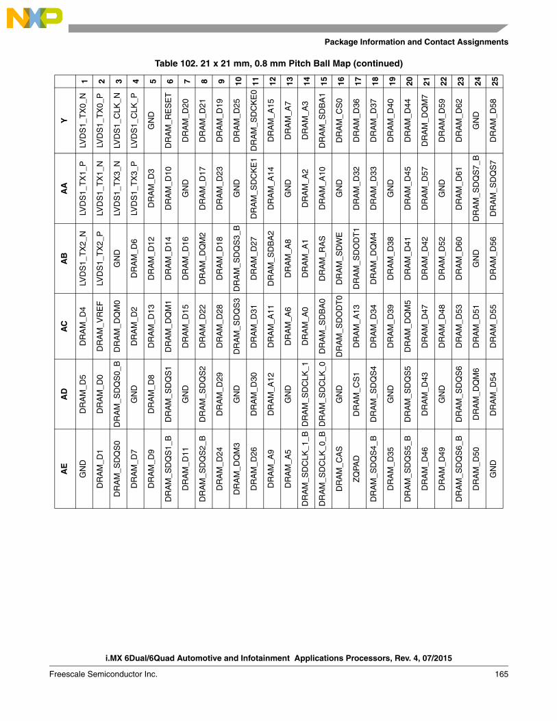
Package Information and Contact Assignments
i.MX 6Dual/6Quad Automotive and Infotainment Applications Processors, Rev. 4, 07/2015
Freescale Semiconductor Inc. 165
Y
LVD
S1_
TX
0_N
LVD
S1_
TX
0_P
LVD
S1_
CLK
_N
LVD
S1_
CLK
_P
GN
D
DR
AM
_RE
SE
T
DR
AM
_D20
DR
AM
_D21
DR
AM
_D19
DR
AM
_D25
DR
AM
_SD
CK
E0
DR
AM
_A15
DR
AM
_A7
DR
AM
_A3
DR
AM
_SD
BA
1
DR
AM
_CS
0
DR
AM
_D36
DR
AM
_D37
DR
AM
_D40
DR
AM
_D44
DR
AM
_DQ
M7
DR
AM
_D59
DR
AM
_D62
GN
D
DR
AM
_D58
AA
LVD
S1_
TX
1_P
LVD
S1_
TX
1_N
LVD
S1_
TX
3_N
LVD
S1_
TX
3_P
DR
AM
_D3
DR
AM
_D10
GN
D
DR
AM
_D17
DR
AM
_D23
GN
D
DR
AM
_SD
CK
E1
DR
AM
_A14
GN
D
DR
AM
_A2
DR
AM
_A10
GN
D
DR
AM
_D32
DR
AM
_D33
GN
D
DR
AM
_D45
DR
AM
_D57
GN
D
DR
AM
_D61
DR
AM
_SD
QS
7_B
DR
AM
_SD
QS
7
AB
LVD
S1_
TX
2_N
LVD
S1_
TX
2_P
GN
D
DR
AM
_D6
DR
AM
_D12
DR
AM
_D14
DR
AM
_D16
DR
AM
_DQ
M2
DR
AM
_D18
DR
AM
_SD
QS
3_B
DR
AM
_D27
DR
AM
_SD
BA
2
DR
AM
_A8
DR
AM
_A1
DR
AM
_RA
S
DR
AM
_SD
WE
DR
AM
_SD
OD
T1
DR
AM
_DQ
M4
DR
AM
_D38
DR
AM
_D41
DR
AM
_D42
DR
AM
_D52
DR
AM
_D60
GN
D
DR
AM
_D56
AC
DR
AM
_D4
DR
AM
_VR
EF
DR
AM
_DQ
M0
DR
AM
_D2
DR
AM
_D13
DR
AM
_DQ
M1
DR
AM
_D15
DR
AM
_D22
DR
AM
_D28
DR
AM
_SD
QS
3
DR
AM
_D31
DR
AM
_A11
DR
AM
_A6
DR
AM
_A0
DR
AM
_SD
BA
0
DR
AM
_SD
OD
T0
DR
AM
_A13
DR
AM
_D34
DR
AM
_D39
DR
AM
_DQ
M5
DR
AM
_D47
DR
AM
_D48
DR
AM
_D53
DR
AM
_D51
DR
AM
_D55
AD
DR
AM
_D5
DR
AM
_D0
DR
AM
_SD
QS
0_B
GN
D
DR
AM
_D8
DR
AM
_SD
QS
1
GN
D
DR
AM
_SD
QS
2
DR
AM
_D29
GN
D
DR
AM
_D30
DR
AM
_A12
GN
D
DR
AM
_SD
CLK
_1
DR
AM
_SD
CLK
_0
GN
D
DR
AM
_CS
1
DR
AM
_SD
QS
4
GN
D
DR
AM
_SD
QS
5
DR
AM
_D43
GN
D
DR
AM
_SD
QS
6
DR
AM
_DQ
M6
DR
AM
_D54
AE
GN
D
DR
AM
_D1
DR
AM
_SD
QS
0
DR
AM
_D7
DR
AM
_D9
DR
AM
_SD
QS
1_B
DR
AM
_D11
DR
AM
_SD
QS
2_B
DR
AM
_D24
DR
AM
_DQ
M3
DR
AM
_D26
DR
AM
_A9
DR
AM
_A5
DR
AM
_SD
CLK
_1_B
DR
AM
_SD
CLK
_0_B
DR
AM
_CA
S
ZQ
PAD
DR
AM
_SD
QS
4_B
DR
AM
_D35
DR
AM
_SD
QS
5_B
DR
AM
_D46
DR
AM
_D49
DR
AM
_SD
QS
6_B
DR
AM
_D50
GN
D
Table 102. 21 x 21 mm, 0.8 mm Pitch Ball Map (continued)
1 2 3 4 5 6 7 8 9 10 11 12 13 14 15 16 17 18 19 20 21 22 23 24 25
i.MX 6Dual/6Quad Automotive and Infotainment Applications Processors, Rev. 4, 07/2015
166 Freescale Semiconductor Inc.
Revision History
7 Revision HistoryTable 103 provides a revision history for this data sheet.
Table 103. i.MX 6Dual/6Quad Data Sheet Document Revision History
Rev. Number
Date Substantive Change(s)
4 07/2015 • Added footnote to Table 1, "Example Orderable Part Numbers," on page 3: If a 24 MHz input clock is used (required for USB), the maximum SoC speed is limited to 996 MHz.
• Section 1.2, “Features” changed Five UARTs, from up to 4.0 Mbps, to up to 5.0 Mbps. • Table 6, "Operating Ranges," on page 21: Row: VDD_HIGH internal regulator, changed minimum
parameter value from 2.8 to 2.7V. • Table 6, "Operating Ranges," on page 21: Removed footnote: VDDSOC and VDDPU output voltages
must be set according to this rule: VDDARM-VDDSOC/PU<50mV. This was a duplicate footnote, renumbered footnotes accordingly.
• Table 6, "Operating Ranges," on page 21: Changed value: Standby/DSM Mode, VDD_SOC_IN, minimum voltage, from 0.9V to 1.05V.
• Table 8, "Maximum Supply Currents," on page 25, Differentiated VDD_ARM_IN, VDD_ARM23_IN, and VDD_SOC_IN by frequency and by Power Virus/CoreMark maximum current.
• Table 21, "XTALI and RTC_XTALI DC Parameters," on page 38, Added rows: Input capacitance; Startup current; and DC input current and their values.
• Table 40, "EIM Bus Timing Parameters," on page 53, Changed WE4–WE17 minimum and maximum parameter values from, 0.5 t (k+1)/2-1.25, to 0.5 x t x (k+1)-1.25.
• Table 41, "EIM Asynchronous Timing Parameters Relative to Chip Select,," on page 60 Added to end of formulas in the minimum, typical, and maximum parameter values for WE31–WE42 and WE45–WE46, × t. For example from 3-CSN, to 3-CSN× t. Also added maximum value to MAXDTI of 10.
• Table 43, "DDR3/DDR3L Write Cycle," on page 63, Changed minimum parameter value of DDR17 from 240 to 125; and of DDR18 from 240 to 150.
• Figure 27, "LPDDR2 Command and Address Timing Diagram," on page 64, LP2 signal cycle reduced. • Table 46, "LPDDR2 Write Cycle," on page 65, Changed LP21 minimum and maximum parameter value
from -0.25/+0.25 to 0.8/1.2. • Figure 41, "ECSPI Master Mode Timing Diagram," on page 76, Added footnote: Note: ECSPIx_MOSI is
always driven (not tri-stated) between actual data transmissions. This limits the ECSPI to be connected between a single master and a single slave.
• Figure 42, "ECSPI Slave Mode Timing Diagram," on page 77, Added footnote: Note: ECSPIx_MISO is always driven (not tri-stated) between actual data transmissions. This limits the ECSPI to be connected between a single master and a single slave.
• Figure 65, "Gated Clock Mode Timing Diagram," on page 98, Corrected IPU2_CSIx_HSYNC trace drawing.
• Section 4.11.23, “USB PHY Parameters” Specified Battery Charging Specification applies to portable devices only.
Revision History
i.MX 6Dual/6Quad Automotive and Infotainment Applications Processors, Rev. 4, 07/2015
Freescale Semiconductor Inc. 167
Rev. 3 02/2014 • Updates throughout for Silicon revision D, include:- Figure 1 Part number nomenclature diagram.- Example Orderable Part Number tables, Table 1
• Feature description for Miscellaneous IPs and interfaces; SSI and ESAI. • Table 2, UART 1–5 description change: programmable baud rate up to 5 MHz. • Table 2, uSDHC 1–4 description change: including SDXC cards up to 2 TB. • Table 6, operating range for Run mode: LDO bypassed, minimum value corrected to 1.150 V. • Table 6, table footnotes, added LDO enabled mode footnote for internal LDO output set points. • Table 61, added table footnote to the Comment heading in the Comment column. • Removed table “On-Chip LDOs and their On-Chip Loads.” • Section 4.1.4, External Clock Sources; added Note, “The internal RTC oscillator does not …”. • Section 4.1.5, reworded second paragraph about the power management IC to explain that a robust
thermal design is required for the increased system power dissipation. • Table 8, Maximum Supply Currents: NVCC_RGMII Condition value changed to N=6. • Table 8, Maximum Supply currents: Added row; NVCC_LVDS2P5 • Section 4.2.1 Power-Up Sequence: reworded third bulleted item regarding POR control. • Section 4.2.1 Power-Up Sequence: removed Note. • Section 4.5.2 OSC32K, second paragraph reworded to describe OSC32K automatic switching. • Section 4.5.2 OSC32K, added Note following second paragraph to caution use of internal oscillator use. • Table 21 XTALI and RTC_XTALI DC parameters; changed RTC_XTALI Vih minimum value to 0.8. • Table 21 XTALI and RTC_XTALI DC parameters; changed RTC_XTALI Vih maximum value to 1.1. • Table 37 Reset Timing Parameters; removed footnote. • Section 4.9.3 External Interface Module; enhanced wording to first paragraph to describe operating
frequency for data transfers, and to explain register settings are valid for entire range of frequencies. • Table 40. EIM Bus Timing Parameters; reworded footnotes for clarity. • Table 41. EIM Asynchronous Timing Parameters; removed comment from the Max heading cell. • Table 41. EIM Asynchronous Timing Parameters; reworded footnote 2 for clarity. • Table 61. RMII Signal Timing; parameter M19 Max value relaxed to 13.5 ns. • Table 77. MLB 256/512 Fs Timing Parameters; added last row for MLBSIG (MLBDAT). • Table 78. MLB 1024 Fs Timing Parameters; added last row for MLBSIG (MLBDAT). • Table 100. Corrected the ALT5 Default Function names. • Figure 106 and Figure 107 21 x 21 mm Lidded Package; updated drawing (Rev D).
Rev. 2.3 07/26/2013
• Table 100, 21 x 21Functional Contact Assignments:Restored NANDF_WP_B row and description.
• System Timing Parameters Table 37, Reset timing parameter, CC1 description clarified, change from:"Duration of SRC_POR_B to be qualified as valid (input slope <= 5 ns)" to: "Duration of SRC_POR_B to be qualified as valid" and added a footnote to the parameter with the following text: "SRC_POR_B rise and fall times must be 5 ns or less."This change was made for clarity and does not represent a specification change.
Rev. 2.2 07/2013 • Editor corrections to revision history links. No technical content changes.
Rev. 2.1 07/2013 • Figure 1, Changed temperature references from Consumer to Commercial. • Table 100, 21 x 21Functional Contact Assignments:
—Removed rows: DRAM_VREF, HDMI_DDCCEC, and HDMI_REF. —Due to a typographical error in revision 2.0, the ball names for rows EIM_DA2 through EIM_DA15 were ordered incorrectly. This has been corrected in revision 2.1. The ball map is correct in both revision 2.0 and 2.1.
Table 103. i.MX 6Dual/6Quad Data Sheet Document Revision History (continued)
Rev. Number
Date Substantive Change(s)
i.MX 6Dual/6Quad Automotive and Infotainment Applications Processors, Rev. 4, 07/2015
168 Freescale Semiconductor Inc.
Revision History
Rev. 2 04/2013 Substantive changes throughout this document are as follows: • Incorporated standardized signal names. This change is extensive throughout.
Added reference to EB792, i.MX Signal Name Mapping. • Figures updated to align to standardized signal names. • Aligned references to FCBGA to read FCPBGA throughout document. • Updated references to eMMC standard to include 4.41. • Table 2, "i.MX 6Dual/6Quad Modules List,” Changed reference to Global Power Controller to read
General Power Controller. • Table 4, "Absolute Maximum Ratings,” Added VDD_ARM23_IN to Core supply voltages. • Table 6 “Operating Ranges ": Run Mode - LDO Enabled, VDD_ARM_IN/VDD_ARM23_IN, 792 MHz,
input voltage minimum changed to 1.275V and VDD_ARM CAP minimum changed to 1.150V. NVCC_NAND, changed to NVCC_NANDF.
• Table 6 “Operating Ranges ": Added reference for information on product lifetime : i.MX 6Dual/6Quad Product Usage Lifetime Estimates Application Note, AN4724.
• Table 9. “Maximum Supply Currents”: Added current for i.MX6Dual • Table 10 “Stop Mode Current and Power Consumption”: Added SNVS Only mode. • Table 22 “GPIO I/O DC Parameters”: Removed parameters Iskod and Isspp. • Table 48, "ECSPI Master Mode Timing Parameters," Updated parameter CS6 ECSPIx_SSx Lag Time
(CS hold time) Min from Half SCLK period to Half SCLK period-2. • Table 77 "SD/eMMC4.3 Interface Timing Specification," eMMC parameter SD8 value Min updated from
5.6 ns to 1.5 ns. • Table 89 RGMII Signal Switching Specifications RGMII parameter TskewR units corrected. • Table 134 "21 x 21 mm Functional Contact Assignments," Updated GPIO_1 Ball Name value to PU
(100K). • Table 134 "21 x 21 mm Functional Contact Assignments," Clarification of ENET_REF_CLK naming. • Removed section, EIM Signal Cross Reference. Signal names are now aligned with reference manual. • Section 1.2, “Features added bulleted item regarding the SOC-level memory system. • Section 4.2.1, “Power-Up Sequence” updated wording. • Section 4.3.2, “Regulators for Analog Modules” section updates. • Added Section 4.6.1, “XTALI and RTC_XTALI (Clock Inputs) DC Parameters”. • Section 4.10, “General-Purpose Media Interface (GPMI) Timing” figures replaced, tables revised.
Table 103. i.MX 6Dual/6Quad Data Sheet Document Revision History (continued)
Rev. Number
Date Substantive Change(s)
How to Reach Us:
Home Page: freescale.com
Web Support: freescale.com/support
Information in this document is provided solely to enable system and software
implementers to use Freescale products. There are no express or implied copyright
licenses granted hereunder to design or fabricate any integrated circuits based on the
information in this document.
Freescale reserves the right to make changes without further notice to any products
herein. Freescale makes no warranty, representation, or guarantee regarding the
suitability of its products for any particular purpose, nor does Freescale assume any
liability arising out of the application or use of any product or circuit, and specifically
disclaims any and all liability, including without limitation consequential or incidental
damages. “Typical” parameters that may be provided in Freescale data sheets and/or
specifications can and do vary in different applications, and actual performance may
vary over time. All operating parameters, including “typicals,” must be validated for each
customer application by customer’s technical experts. Freescale does not convey any
license under its patent rights nor the rights of others. Freescale sells products pursuant
to standard terms and conditions of sale, which can be found at the following address:
freescale.com/SalesTermsandConditions.
Freescale and the Freescale logo are trademarks of Freescale Semiconductor, Inc. Reg.
U.S. Pat. & Tm. Off. All other product or service names are the property of their
respective owners. ARM, Cortex, TrustZone, and NEON are registered trademarksof
ARM Limited (or its subsidiaries) in the EU and/or elsewhere.
© 2012-2015 Freescale Semiconductor, Inc. All rights reserved.
Document Number: IMX6DQAECRev. 4
07/2015