Hamamu: Specializing FPGAs for ML Applications by Adding ...
FPGAs in Industrial Control Applications
Eric Monmasson, Senior Member, IEEE, Lahoucine Idkhajine, Member, IEEE,
Marcian N. Cirstea, Senior Member, IEEE, Imene Bahri, Student Member, IEEE, Alin Tisan, Member, IEEE, and
Mohamed Wissem Naouar, Member, IEEE
Abstract - The aim of this paper is to review the state of the art
of Field Programmable Gate Array (FPGA) technologies and
their contribution in industrial control applications. Authors
start by addressing various research fields where FPGAs are
useful. The features of these devices are then presented
followed by their corresponding design tools. To illustrate the
benefit of using FPGAs in the case of complex control
applications, a sensorless motor controller has been treated.
This controller is based on the Extended Kalman Filter. Its
development has been made according to a dedicated design
methodology which is also discussed. Another example of
illustration is the Neural Network Systems. To show the
interest of FPGAs in this field, some case studies have been
presented.
Index terms – Field Programmable Gate Array, Industrial
Control Applications, System on Chip, Design Tools, Design
methodology, Sensorless Motor Controller, Extended Kalman
Filter, Neural Network Systems
I- INTRODUCTION
Nowadays, to make the difference on the market, new
industrial control systems have to be highly performing,
very flexible and reliable.
At the same time, the cost is a key issue. In order to
reduce it, time-to-market has to be shortened, the price of
controller device has to be cheap and its energy
consumption as well as the one the controlled system
reduced.
This cost reduction is all the more challenging that these
new industrial control systems must be based on ever
increasing sophisticated control algorithms which need a lot
of computing resources and need reduced execution time.
To cope with all these challenges, designers can rely on
more and more mature digital electronics technologies that
come along now with friendly software development tools.
To implement efficient real-time industrial control
systems, designers have the choice between two main
families of digital device technologies.
The first family is based on a pure software platform.
The associated devices are microcontrollers and Digital
Signal Processor controllers (DSP controllers). These
components integrate a performing microprocessor core
along with several peripherals which are necessary to
control the targeted system in real-time and to communicate
with the industrial environment.
The difference between microcontrollers [1] and DSP
controllers [2] is, for a given surface of silicon, the ratio
between the processing unit and the communication and
control peripherals. The microcontrollers include a general
purpose 16-bit or 32-bit Reduced Instruction Set Computer
(RISC) and a wide variety of peripherals, while DSP
controllers integrate a high performing processor core based
on an hardware accelerator computing block (Multiply and
Accumulate Arithmetic Logic Unit MAC ALU) and few
peripherals. However, the limits between these two concepts
are vanishing since the RISC unit of microcontrollers is
more and more powerful and the number and the types of
peripherals in DSPs are increasing.
The main advantages of this approach are the maturity of
these technologies, the quality of the associated
development tools as well as their low price. The main
limitations are the difficulty to take advantage of the
potential parallelism offered by the control algorithm to be
implemented and as a consequence, the limitation of the
performances in terms of throughputs and achievable
bandwidth.
The alternative family of available digital devices for
implementing industrial control systems is the Field
Programmable Gate Arrays technology (FPGAs) [3]. These
devices consist of pre-designed elementary cells and
interconnections that are fully programmable by the end
user to build specific hardware architectures that match the
requirements of the final targeted application.
The variety of the designed FPGA-based controllers is
large. As shown in section II, current FPGAs allow the
implementation of efficient 32-bit RISC processors. As a
consequence, FPGAs can be first viewed as programmable
microcontrollers where designers can combine one or
several RISC processors with dedicated peripherals and
computing hardware accelerators. From this perspective and
due to their ever increasing density, modern FPGAs can be
seen as true System-on-Chip (SoC) digital platforms.
To the other side of the range, designers can also design
pure specific hardware architectures for stringent
applications in terms of performances. Thus, the design and
the real-time implementation of control loop with sampling
frequency above one MHz are now possible thanks to this
approach as well as the implementation of massive parallel
treatments.
Like microcontrollers and DSPs, FPGAs were born in
the eighties and are now a mature technology. FPGA design
tools are also very friendly. As mentioned before, FPGAs
are suited for high speed demanding applications. Indeed,
designers can develop a fully hardware architecture which is
dedicated to the control algorithm to implement. Hence, by
preserving the potential parallelism of the algorithm, the
resulting hardware architecture allows matching the
expected processing speed specifications.
The main limitation of this technology is the cost.
FPGAs are still more expensive compared to their DSP and
microcontroller competitors although this claim has to be
revised. Indeed, FPGA may be more expensive than a
microcontroller but not the cost per implemented function.
Another drawback concerns the difficulty to integrate
within current FPGAS mixed Analog/Digital peripherals
like A/D and D/A converters. Once again, this limitation is
vanishing with the recent introduction on the market of
FPGAs that integrate A/D converters [4].
The success of a recent Special Section devoted to the
use of FPGAs to control Industrial Control Systems [5]-[6]
has demonstrated the great interest of this technology among
the research community.
Indeed, the ceaseless increasing density of FPGAs along
with their high degree of flexibility pushed designers to use
them for controlling a large range of industrial applications.
The most significant are now reminded.
A. FPGA-based controllers for embedded industrial and
robotic applications
Automotive and aircraft embedded systems are very
challenging applications for digital electronics [7]. For these
systems, safety is of prime importance. Thus, in [8] and [9]
authors have proposed several techniques to tackle this issue
and enhance reliability of the FPGA-based controllers.
Another aspect of safety is the possibility for vehicle
manufacturers and their suppliers to cope with the
obsolescence of critical embedded systems. Electronic
devices have now a very limited life time and it is
mandatory to still find in the market fully secure FPGA-
based Intellectual Property (IP) module to replace them
when they are now longer available [10]. The current trend
for modular architecture within the FPGA-based embedded
controller has also pushed designer to reinforce Intellectual
Property by the use of sophisticated encryption techniques
[11].
Another concern for automotive and aircraft embedded
systems is the design and real-time implementation of high
data rate and reliable protocols for in-vehicle networks such
as FlexRay or SpW [12]-[13].
Regarding handheld embedded systems, the key issue is
the reduction of power consumption [14]-[15]. The notion of
power budget is now considered during the design process.
In this field, several studies have evolved. In [16], a deep
understanding of the source of power consumption and
guidelines for its minimization are presented.
FPGA devices are also welcome for managing the
communication distributed applications via the efficient
real-time Ethernet protocol [17]-[18].
Finally, mention that FPGAs are highly appreciated in
the field of robotics. Sensor-based construction of efficient
geometric structures via the generalized Voronoi diagram
(GVD) have been implemented with success in FPGAs for
mobile robots [19-20]. In [21], a coarse-grain parallel
deoxyribonucleic acid (PDNA) algorithm for optimal
configurations of an omnidirectional mobile robot with a
five-link robotic arm is presented.
In [22] and [23] examples are presented of FPGA-based
controllers for haptique and tele-operation robotics.
B. FPGA-based controllers for power electronics and drive
applications
A detailed analysis of the benefits of using FPGA-based
controllers in power electronics and drive applications can
be found in [24]. Just the salient features of this analysis are
reminded here. Nowadays, the more limiting factor of
current or voltage control loop of a power converter is the
limitation of the switching frequency due to switching
losses. Thus, the choice of the sampling frequency is most
of the time conditioned by the maximum available switching
frequency. Based on this analysis, two different groups can
be identified:
- High demanding applications
- Constrained switching frequency applications.
This first group concerns applications where the use of
FPGA-based controllers is mandatory due to stringent
constraints in terms of time or parallelism.
The parallelism constraint case concerns the control of
static converters where power is distributed in order to
reduce the stress of the power switches. In these cases,
concurrency is high since several power channels have to be
driven in parallel. A good example of highly parallel
operations can be found in [25] where a combined
multiphase multilevel (5 phases, 5 levels) Space Vector
Pulse Width Modulation (SVPWM) strategy was
implemented with success in a low cost FPGA.
The time constraint case concerns applications where the
sampling frequency is very high (at least equal or above 100
kHz) like for low voltage switch mode power supplies
(SMPS). For such applications, the used switching
frequency is equal or above 1MHz FPGA-based controllers
are in this case mandatory [26]-[28].
Another high demanding application concerns hardware
and power Hardware-In-the-Loop applications (HIL). In
[29], authors present a FPGA-based real-time digital
simulator of a 3-level 12-pulse Voltage Source Inverter
(VSI) fed induction machine drive. It is worth to be
mentioned that the VSI model is computed at a fixed time-
step of only 12.5ns, allowing a realistic representation of the
IGBT nonlinear switching characteristics and power losses.
The second group consists in applications where
sampling is not critical due to switching frequency
limitation. For this kind of applications, the use of a
software-based controller is possible. However, even in this
case, using FPGA can be of great interest since this way,
control processing time can be drastically reduced, up to a
fraction of the sampling period. This rapidity has an
immediate influence on the quality of the control
performances, especially when direct control is chosen [30].
Thus, the behavior of the proposed digital controller is very
closed to its analog counterpart. Besides, due to the ever
increasing density of the FPGA components, one can now
implement complex algorithms within a few microseconds.
A sensorless controller based on the Extended Kalman Filter
(EKF) will be discussed later on (section III) to illustrate
this trend. Other improvements due to rapidity of the
controller are,
- The reduction of complexity: In [31] a simple fault tolerant
controller for wind energy conversion systems is presented.
It is based on the combination of time and magnitude
thresholds which allows reducing significantly the time for
default detection (less than 10µs) where standard solutions
need at least one quarter of the fundamental period.
- Synchronization between the current sampler and the
PWM carrier. In [32], an FPGA-based implementation of a
Switched Reluctance Motor (SRM) current control without
anti-aliasing filters is presented. Indeed, by choosing to
sample current in the center of a symmetrical modulation, an
exact measure of the average current is obtained without any
additional filter.
- Shared control resources: It consists in controlling several
similar plants with a unique controller. Thus, in [33],
authors have proposed an FPGA-based controller that is able
to control up to 4 AC-drives with a sampling period of only
50µs. Other interesting multi-axis controllers are given in
[34].

- Oversampling strategies which are mainly used for
improving the quality of the measurement of quantities. For
instance, in [35], authors present a quasi-ideal direct
measuring of the mean value of the current feedback.
- Adding of new control functionalities: From this
perspective, a real-time processing extension that naturally
comes to mind is the implementation of a predictive control
strategy like the one presented in [34] for synchronous
motor drives. Another exciting challenge is the addition of
health-monitoring processing. Very promising works have
already been proposed for SMPS applications, like in [36]
where an on-line identification strategy through cross-
correlation was successfully implemented. In the same vein,
diagnosis algorithms can also be implemented. To this
purpose, [37] and [38] have proposed wavelet-based
diagnosis algorithms for respectively induction motor
broken-rotor-bar detection and fault detection and
classification in transmission lines.
This paper is aimed to explain the importance of FPGA-
based solutions in the design of industrial control systems.
The second section recalls the main features of the available
FPGA technologies. Then, in the third section, an in-depth
of a complex FPGA-based controller example is treated. It
consists in a FPGA-based sensorless controller for
synchronous motor using an Extended Kalman Filter (EKF).
All the steps of the design are described and comparisons
are given in terms on software and hardware
implementations. Section IV is devoted to Artificial Neural
Network (ANN) based FPGA-Systems. There is a growing
interest for implementing ANN within FPGA mostly
because their inherent parallelism. Two case studies are
presented: a highly compact PWM generator and an
electronic nose. Finally, conclusions are given and future
trends given.
II- PRESENTATION OF FPGAS
Since their first introduction to the market in 1985 by the
Xilinx Company, FPGA hardware technologies have
attracted an always increasing interest and have significantly
disrupted the early digital development process trends.
Indeed, these devices belong to the so called semi-custom
ASICs (Application Specific Integer Circuits). The latter
low cost devices consist of pre-designed (by the
manufacturer) elementary cells and interconnections that
can be programmed and interconnected by the user. This has
the credit to allow rapid-prototyping solutions and make the
design process more flexible and cheaper. This is not the
case of full-custom ASICs that are manufactured for a
specific application and cannot be re-programmed by the
user.
A. Generic structure of an FPGA.
As presented in Fig. 1, the basic structure of an FPGA
consists of a sea of Logic Blocks (LBs), of an
interconnection network and configurable I/O blocks.
Because of their very high level of integration, in the recent
FPGA devices are also included memory blocks, hardwired
DSP blocks, clock manager blocks and communication
blocks [41].
Fig. 1. Generic structure of an FPGA
Depending on the expected function to implement, each
LB is configured to perform combinatorial and/or sequential
operations. For the combinatorial operations, a set of Look-
Up-Tables (LUTs) are included. This is the same for the
sequential operations with a set of D-Flip-Flops. An LB is
also able to perform a local storage function (distributed
RAM memory), shift register (SR), multiplexer, and
adder/subtractor operations. The interconnection network is
also programmable by the user so as to interconnect as many
LBs as necessary.
0
100000
200000
300000
400000
500000
600000
700000
800000
900000
Logic cells 100 484 1024 1296 12160 27648 51840 99216 200448 337500531200 758784 813050
1985 1987 1990 1992 1995 1998 1999 2002 2004 2006 2008 2009 2010
Fig. 2. Evolution of the FPGA density
On the other hand, the internal structure of LBs differs
from an FPGA family to another. For this reason, a
normalized FPGA density metric has been accepted. Indeed,
a common Logic Cell (LC) has been defined. It consists of a
4-bit LUT, a D-Flip-Flop, a carry chain (for arithmetic
operations) and a multiplexer, [39]-[42]. Fig. 2 presents the
evolution of FPGAs in terms of density (i.e. number of the
available LCs) since 1985. The waveform has been obtained
after a comparison of the commercialized FPGA devices
within each year.
The configurable I/O blocks allow the interfacing
between the internal architecture and the external
environment.
In order to optimize FPGA resources, hardwired DSP
blocks (arithmetic blocks) including multipliers, adders and
accumulators are included. For the same purpose, memory
blocks (RAM, ROM, Flash RAM) are also integrated.
The integrated clock manager blocks allow the
management of the clocking resources. They are commonly
based on Phase-Locked-Lools (PLLs). The latter support
several features such as frequency multiplication and
division, propagation delay compensation and phase shift
correction.
The current FPGA devices include also communication
blocks that consist generally of transmission and reception
buffers. Various communication protocols are supported,
including among others USB, Ethernet, CAN, PCI, SPI and
I2C protocols.
I/O blocks
Interconnection network
Logic blocks
Clock management blocks
Memory blocks Arithmetic (DSP)
blocks
Communication
blocks
Embedded
processor core
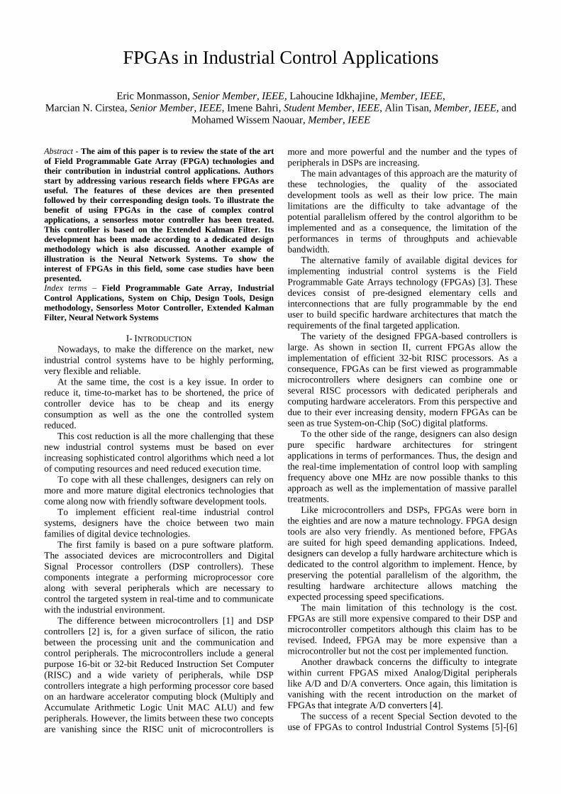
To provide high integration density, high speed and low
power consumption, FPGAs have been the subject of a
considerable progress in terms of copper process
technology. Recent devices are now reaching down to 40
nm copper process (28nm has been recently announced by
Xilinx and Altera vendors) [39], [40]. Fig. 3 shows the
evolution of the process technology since 1985.
0
200
400
600
800
1000
1200
1400
1600
1800
2000
Process technology (nm)
Techno (nm) 2000 1200 800 420 334 220 130 90 65 40 40 40
1985 1987 1990 1992 1995 1998 2002 2004 2006 2008 2009 2010
Fig. 3. Evolution of the FPGA process copper technology
The internal structure, the operating mode and the
configuration of these FPGA elements differ depending on
the device family and technology. There are various
configuration technologies including, SRAM, EPROM,
EEPROM, Fuse, Antifuse and Flash technologies. Because
of their popularity, only the SRAM and the Flash
technologies will be discussed.
Besides the evolution of these FPGA technologies and in
order to meet flexibility and high integration capability, the
novel FPGA devices give the possibility to implement an
increasing diversity of cores. Indeed, in addition to the
previously presented FPGA cores and as it will be discussed
afterwards, FPGA can integrate one or several processors
and even analog peripherals [45]-[53]. They are then
considered as System-On-Chips (SoCs) or System-on-
Programmable-Chips (SoPCs) solutions.
B. FPGA internal technologies and architectures
1- SRAM based FPGAs
The configuration of an SRAM-based FPGA is entirely
made using a set of dedicated SRAM blocks. These blocks
are organized as a specific configuration layer. This
programming strategy is volatile and a reconfiguration of
the devices is required after the device is switched off. The
most popular SRAM-based FPGA families are Xilinx and
Altera families, [39], [40]. Among the commercialized
FPGA devices, one can stress the high performance
VIRTEX (Xilinx) and STRATIX (Altera) FPGAs and the
low cost SPARTAN (Xilinx) and CYCLONE (Altera)
FPGAs. In the field of industrial control applications, cost is
a key-issue. As a consequence, the low cost families are
preferred. Thus, only the latest Xilinx SPARTAN-6 and
Altera Cyclone-4 FPGA families will be presented.
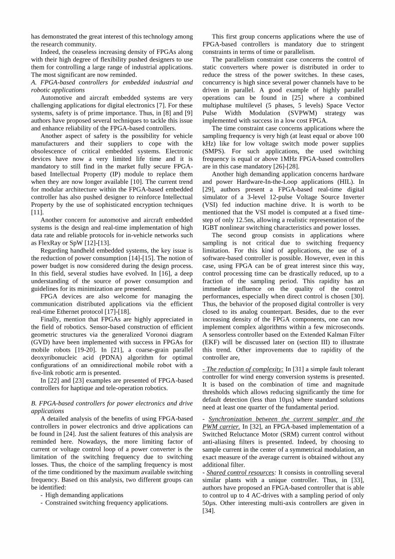
Xilinx SPARTAN-6 FPGA: As shown in Fig. 4, this
SRAM-based FPGA incorporates a sea of CLBs
(Configurable Logic Blocks) and an interconnection
network [39]. Roughly speaking each CLB is equivalent to
12.8 LCs.
A CLB contains a pair of slices, the SLICEX and
SLICEL/SLICEM. Each slice can be configured to perform
combinatorial functions using four 6-bit LUTs and
sequential functions using eight D Flip-Flops. The SLICEM
can also be configured to perform a distributed RAM block
for data storage [39]. Consequently, there are 50% of
SLICEX, 25% of SLICEM and 25% of SLICEL inside the
SPARTAN-6 device (see Fig. 4).
Fig. 4. SRAM-based SPARTAN-6 FPGA
Altera CYCLONE-4 FPGA: The structure of the
Cyclone-4 FPGA is presented in Fig. 5. In this case, the
logic cells are named Logic Elements (LE). Roughly
speaking each LE of an Altera FPGA is equivalent to one
LC.
Fig. 5. SRAM-based CYCLONE-4 FPGA
The LEs are gathered in 16-group blocks called Logic
Array Blocks (LAB). A LE consists of a 4-bit LUT that can
perform either combinatorial or arithmetic operations and a
D-Flip-Flop for sequential operations. The interconnection
blocks are organized in 2 levels; local interconnection
network and global network, [40]. Table I: SRAM-based FPGA - some specifications
SPARTAN 6 CYCLONE 4
Number of LCs 147443 (11519 CLBs) 150000
I/Os 576 532
DSP blocks 180 DSP blocks 360 Multipliers
Clocking performances:
PLL output frequency range 400-1080 MHz 600-1300 MHz
Memory size (RAM, ROM) 6179 Kb (RAM blocks
and distributed RAM) 6480 Kb (RAM
blocks)
Process technology 45 nm 60 nm
Table I presents some important specifications regarding
the SRAM-based FPGAs (SPARTAN-6 and CYCLONE-4).
It indicates the maximum available characteristics
depending on the FPGA series.
2- Flash based FPGA
In the case of Flash technology, the configuration is
based on flash connections that keep the configuration state
when the power is off. Each connection contains two
transistors that share a floating gate and stores the
programming information, [4]. This technology is the most
useful technology in aircraft and space systems since it
guaranties the configuration against the SEU (Single Event
Upset) radiations. In the proposed survey, the Actel Fusion
Flash-based FPGA is presented. Its internal logic cells
consist of VersaTiles (VTs). The latter can implement either
a combinatorial (3-bit LUT) or a sequential (D Flip Flop)
functions. Fig. 6 gives an overview of the Fusion FPGA
structure.
LAB
LE1
LE2
LE16 Local
network
LA
B
LA
B
LA
B
Global
network
CLB
SLICEM or
SLICEL SLICEX
Switch
matrix Interconnection node
6-transistor based
connection point
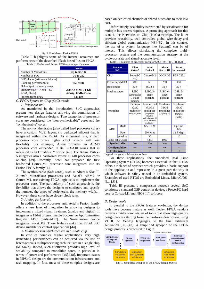
Fig. 6. Flash-based Fusion FPGA
Table II highlights some of the internal resources and
performances of the described Flash-based Fusion FPGA. Table II: Flash-based Fusion FPGA- some specifications
Fusion
Number of VersaTiles Up to 38.5 K
Number of I/Os Up to 252
DSP blocks (arithmetic blocks) 0
Clocking performances:
PLL output frequency range 350 MHz
Memory size (RAM/FIFO,
ROM, Flash)
270 Kb (RAM); 1 Kb
(ROM); 8 Mb (Flash)
Process technology 130 nm
C. FPGA System on Chip (SoC) trends
1- Processor unit
As mentioned in the introduction, SoC approaches
present new design features allowing the combination of
software and hardware designs. Two categories of processor
cores are considered, the “non-synthesizable” cores and the
“synthesizable” cores.
The non-synthesizable (also called hard processor cores)
have a custom VLSI layout (in dedicated silicon) that is
integrated within the FPGA. As a general rule, a hard
processor core offers higher clock speeds with less
flexibility. For example, Altera provides an ARM9
processor core embedded in its EPXA10 series that is
marketed as an Excalibur™ device [40]. The Xilinx Virtex-
5 integrates also a hardwired PowerPC 440 processor cores
on-chip [39]. Recently, Actel has proposed the first
hardwired Cortex-M3 processor core integrated into its
Fusion FPGA family [4].
The synthesizable (Soft cores), such as Altera’s Nios II,
Xilinx’s MicroBlaze processors and Actel’s ARM7 or
Cortex-M1, use existing FPGA logic cells to implement the
processor core. The particularity of such approach is the
flexibility that allows the designer to configure and specify
the number, the types of peripherals, the memory width…
However, these cores have slower clock rates.
2- Analog peripherals
In addition to the processor unit, Actel’s Fusion family
offers a new level of integration by allowing designer to
implement a mixed signal treatment (analog and digital). It
integrates a 12-bit programmable Successive Approximation
Register ADC (SAR-ADC). The SmartFusion device
integrates two ADCs. These features make this FPGA SoC
device suitable for control applications [44].
3- Multiprocessing architectures in a single chip
In case of complex digital applications, very high
demanding performances can be achieved via the use of
heterogeneous multiprocessing architectures in a single chip
(MPSoCs). Indeed, such alternative provides high level of
scalability compared to monolithic cores, in particular in
terms of power and performance [45]-[48]. Important issues
in MPSoC design are the communication infrastructure and
task mapping. In fact, most of these complex designs are
based on dedicated channels or shared buses due to their low
cost.
Unfortunately, scalability is restricted by serialization for
multiple bus access requests. A promising approach for this
issue is the Networks on Chip (NoCs) concept. The latter
provides reusability, well-controlled global wire delay and
efficient global communication [48]-[52]. In this context,
the use of a system language like SystemC can be of
interest. This allows simulating the complete multi-
processor system and the communication strategy at the
cycle-accurate and signal-accurate level. Table III: Features of processor cores for SoCs [39], [40], [4], [63]
Features
SoC Xilinx
Virtex-5
Actel
Fusion 1
Altera
Startix III
Texas
Intruments1
CPU PowerPC
440
Cortex-M1 NIOS II/f DSP C28x
Frequency (MHz) 400 60 290 150
Bit Number 32 b 16/32 b 32 b 32 b
Pipeline stages RISC
superscalar7-stage
pipeline
RISC, 3-
stage pipeline
RISC, 6-
stage pipeline
DSP, 8-
stage pipeline
Multiplier
Hardware
32x32 multiplier (single cycle)
Synthesizabl
e32x32 multiplier (3 cycle for
standard
multiplier and 33
cycle for small
multiplier)
Hardware
32x32 multiplier (single cycle)
Hardware
32x32 multiplier
(single
cycle)
ADC
Mode SAR -12b Pipeline-12b
Rate 600 Ksps 12.5 Msps
pipeline 30 16
Logic cells Usage 4353 1020
Synthesizable No Yes Yes No
Configurability ++ ++ ++ --
Performance ++ + + ++
Legend: ++ good; + Moderate; -- Poor
For these applications, the embedded Real Time
Operating System (RTOS) becomes essential. In fact, RTOS
offers a rich set of services which provides a basic support
to the application and represents in a great part the way in
which software is safely reused in an embedded system.
Examples of used RTOS are Embedded Linux, MicroC/OS-
II… [53].
Table III presents a comparison between several SoC
solutions: a standard DSP controller device, a PowerPC hard
core, a Cortex-M1 and NIOS II/f soft core.
D. Design tools
In parallel to the FPGA features evolution, the design
tools have become mature as well. Today, FPGA vendors
provide a fairly complete set of tools that allow high quality
design process starting from the hardware description, using
VHDL or Verilog languages, to the final bitstream
generation [39]-[42]. A simplified synoptic of the FPGA
design process is presented in Fig. 7.
Fig. 7. Simplified synoptic of the FPGA design process
Design
synthesis
VHDL/Verilog
coding + IP
blocks
FPGA I/O
assignment
Map, Place
and Route
Bitstream
generation and
device
configuration
Simulation
Functional
validation
Simulation
Post-synthesis
validation
Simulation
Post-Route
validation
Physical implementation
Versa
Tile
Flash switch
VersaTile- flash switches based configuration

Generally, design tools include hardware design and
verification tools (VHDL/Verilog editor, synthesizer,
place/route and physical implementation tools), vendor
libraries in addition to simulation and debugging tools.
Some examples are the Integrated Software Environment
(ISE) tools from Xilinx, Quartus tools from Altera and
Libero Integrated Design Environment (LiberoIDE) tools
from Actel. All of them provide flexible and complete
design features with additional associated tools for
simulations (e.g. ModelSim tools) and for debugging (e.g.
ChipScope tools from Xilinx).
Fig. 8. Typical FPGA SoC design flow
Furthermore, to suit SoC trends, FPGA vendors provide
software development tools (editor, compiler, assembler,
linker and debugger), software vendor IPs and processor
customization tools. For example, Xilinx provides
Embedded Development Kit (EDK) platform, Altera
provides Embedded Design Suite (EDS) platform and Actel
provides SoftConsole platform. Fig. 8 presents a standard
design flow for developing SoC applications.
This design flow consists of two main procedures: the
software design Flow and the hardware design Flow. It
offers a user-friendly interface that allows the designer to
customize the processor for a specific project. After its
configuration, the processor core is generated in the form of
an HDL file (in the case of Altera and Actel tools) or a
netlist file (in the case of Xilinx tools). Then, this file can be
associated to custom user logic and integrated within the
hardware design flow to be synthesized, placed and routed.
The FPGA can be configured with the resulting bistream
file. Then, the program which will be integrated on the soft
processor cores can be compiled with the associated library
files and C header files. A C/C++ compiler targeted for this
processor is also provided for the development system.
III- FPGA-BASED DESIGN OF AN INDUSTRIAL CONTROLLER
CASE STUDY: SENSORLESS MOTOR CONTROLLER BASED ON
AN EXTENDED KALMAN FILTER
FPGA technology allows the development of hardware
architectures within a flexible programmable environment.
This feature gives designer an additional degree of freedom
compared to software implementations based on
microcontrollers and DSPs [42], [43]. This is because
FPGAs are outperforming these software solutions by
exploiting the inherent parallelism of the algorithm.
Consequently, designer can develop a hardware architecture
that is fully dedicated to the algorithm to implement. Thus,
the execution time is drastically reduced. Regarding an
industrial control application, the reduction of the execution
time makes the control quasi-instantaneous. The control
bandwidth is then enhanced.
On the other hand, the development of a dedicated
hardware architecture can be seen as intuitive and not
adapted to the implementation of more and more complex
controllers. This is the reason why the use of a well-
structured design methodology is quite important. Such a
methodology should consist of a set of steps and rules to be
followed in order to make the design process more
manageable and less intuitive.
In this section, the FPGA-based design of an industrial
controller is discussed. In order to show the benefit of using
FPGA for complex controllers, a sensorless motor controller
is presented. This controller uses an Extended Kalman Filter
(EKF) to estimate the rotor speed and position of the used
synchronous motor. This development is made according to
the design methodology, [42]-[44], overviewed in Fig. 9.
Fig. 9. FPGA-based controller design methodology
The particularity of this methodology consists in
providing a top-down design process that starts from the
preliminary system specification to the final experimental
validation. In addition, a notable distinction between the
development of the algorithm and its digital implementation
is made. This distinction has the credit of making the
algorithm totally independent of the used digital device. For
instance, once the developed algorithm is achieved, either a
hardware solution (FPGA) or a software solution (DSP) can
be chosen. Furthermore, this distinction can lead to a
separation between the needed designer qualifications. For
example, the algorithm development may be realized by
control engineers and the FPGA development by a micro-
electronics expert.
From a more technical point of view, the proposed
design methodology includes optimization assumptions that
ought to be achieved so as to adapt the algorithm complexity
to the available FPGA resources. As it will be discussed
later, this optimization is done during the algorithm
development process and during the FPGA architecture
development one. For the first case, this consists in reducing
the computational cost of the algorithm (reduction of the
number of processed operations). As for the second case,
this consists in studying the data dependency of the
algorithm and finding out the potential factorizations that
lead to the use of a minimum of operators that process a
maximum of operations. This optimization can be achieved
by applying for example the so-called Algorithm
Architecture Adequation (A3) methodology [30].
A. Preliminary system specification
In this first step, the preliminary specification of the
whole sensorless control application is made. To this aim, a
Configure
Processor
ppppProcesso
rProcessProcessor
FPGA Synthesis
Tool
C/C++ Compiler
for Processor
FPGA
Place and Route
Configure
Peripherals IP
ppppProcessorP
rocessProcessor
HDL
Netlist
User
Hardware IPs
Application
Program
Hardware Design
Flow
Software Design
Flow
Processor core
Configuration Flow
µP RAM
ROM
User Logic
Peripheral
drivers
RTOS
HDL Preliminary system specification
Algorithm development
Experimentation
Modular partitioning
Continuous-time functional validation
Digital realization
Algorithm optimization
Discrete-time, fixed-point validation
Hardware In the Loop validation
Experimental validation
FPGA architecture design Architecture optimization
Architecture design
Architecture VHDL/Verilog coding
Architecture functional simulation
Design synthesis and time/area performances analysis
FPGA physical implementation process

hardware specification and an algorithm benchmarking are
achieved.
Fig. 10. Sensorless control system
The hardware specification consists in choosing,
depending on the load conditions, the AC motor to be
controlled and the appropriate power supply system. In
addition, the sensors, the digital control unit and the ADC
interfaces are defined. The algorithm benchmarking consists
in choosing the control strategy and in specifying the
sensorless method.
In the proposed application, the controlled AC drive
consists of a salient Synchronous Motor (SM) fed by a
Voltage Source Inverter (VSI). The sensorless controller is
based on an Extended Kalman Filter (EKF) which estimates
the rotor position and speed [54]-[62]. An overview of the
implemented control system is presented in Fig. 10.
The EKF estimation is based on the normalized d-q
stochastic system model (relations 1-3). This model is
derived under the “infinite inertia” hypothesis [54]-[62].
vxHy
wuxfx
nn
nnn
),(
T
B
sq
B
sdn
T
B
sq
B
sdn
T
B
e
B
e
B
sq
B
sdn
I
i
I
iy
V
v
V
vu
I
i
I
ix
;;
T
n
sqB
B
sdB
B
en
B
B
enB
sq
rndsr
snd
sq
sd
snq
sq
s
snqenB
sd
sq
snd
sd
s
nn HuLI
V
LI
V
L
IMi
L
Li
L
R
iL
Li
L
R
uxf
00
00
10
01
;
00
00
0
0
0
)(),(
Where f and H are the state space and the output
matrices. xn is the normalized state space vector. un and yn
are respectively the normalized system input and output
vectors. (isd ,isq) and (vsd ,vsq) are respectively the d-q stator
currents and stator voltages. (Lsd ,Lsq) are the stator
inductances and Rs is the stator resistance. θe and ωe are
respectively the rotor position and speed. VB, IB, ωB, θB are
the base values for normalisation. n is the normalization
index. The model and measurement disturbances are
statistically described by the zero-mean Gaussian noises w
and v respectively characterized by covariance matrices Q
and R.
In the following, we are going to present the EKF basics.
To start with, relation (4) presents the discrete-time
stochastic state space model of the observed system. fd is the
discrete time state space matrix and k is the sampling index.
Table IV summarizes the EKF equations.
knknk
knknkdnk
vxHy
wuxfx
),( 11
Table IV: EKF Algorithm
Prediction Step
),ˆ(ˆ11/11/ nkknkdknk uXfX
EKF Compensator
Jacobian matrix :
1/1ˆ
knkxx
d
dnkx
fF
Covariance matrix prediction :
QFdPFdP t
nkknknkknk .. 1/11/
Initial condition P0
Kalman gain calculation :
1
1/1/ ..
RHPHHPK t
knk
t
knknk
Updating covariance matrix :
1/1// knknkknkknk PHKPP
Innovation step
1/1//ˆˆˆ
knknknkknkknk XHyKXX
The implemented stator current controller is based on
Anti-windup PI regulators [30], [53]. This PI controller
calculates the d-q voltage references according to the
measured and reference currents. After a coordinate
transformation, the 3-phase voltage references are
processed. Then the used Carrier-Based Pulse Width
Modulation (CB-PWM) generates the PWM signals for the
VSI. The speed controller is made up using a Proportional-
Proportional Integral (P-PI) regulator that is deeply studied
in [53].
As far as rotor current is concerned, a hysteresis
controller and a buck converter have been implemented in
order to maintain the rotor current equal to a constant value
[30]. The voltage interface aims to generate the 3-phase
stator voltages after a multiplication of the per-unit voltages
(from the controller) by the measured DC link voltage.
B. Algorithm development
The algorithm development process consists of a set of
steps during which the designer makes the functional
validation and prepares the algorithm for digital
implementation.
1- Modular partitioning
The modular partitioning consists in dividing the whole
sensorless algorithm into independent and reusable modules
with different levels of granularity. For the chosen example,
the extracted modules are those presented in Fig. 10.
2- Continuous-time functional validation
Once the control system is designed and the algorithm
partitioning is made, a continuous-time (s-domain)
functional simulation is achieved using Matlab/Simulink
tools. This step is aimed to simulate and verify the
functionality of the complete control system.
3- Digital realization
During this step, the first task consists in making a
digital synthesis of the aimed control closed loop. Two
approaches are considered, the direct synthesis approach and
the digital re-design approach. The first one consists in
configuring the controller and synthesizing the used
regulators in a fully discrete-time z-domain. The re-design
approach consists in synthesizing regulators in the
Voltage Source
Inverter
Digital Sensorless Control Unit
PI-based Current Controller
SM LOAD
EKF Module
e
Isd* = 0A Isq*
S
a
S
b
S
c
isa, isb VDC
Voltage interface
isa, isb
Vsa
*
Vsb
*
Vsc
*
CB-PWM
Buck converte
r
Hysteresis Controller
Ird*
Ird
ADC
e sdi
sqi
P-PI based Speed Controller
ωe*
Vsa Vsb Vsc
Vsa*,Vsb*, Vsc*
(1)
(2)
(3)
(4)
(6)
(5)
(7)
(8)
(9)
(10)
continuous s-domain and then making the convenient
transformation to the discrete-time domain (ZOH, Tustin,
Euler).
The speed and current regulators have been synthesized
using the re-design approach using the Tustin
transformation. The EKF has been synthesized using the
direct synthesis approach but its prediction module is based
on the re-designed system model. For the latter, the Euler
transformation method is used. The chosen sampling
frequency is set to 10 KHz.
The obtained digital controller and observer can be
considered as digital filters that are now to be realized. Their
structures are then specified (direct form, cascade form,
transpose form …).
The following task is the choice of the fixed point data
format. This choice can be made in two stages [64]. The first
one is the choice of the fixed-point format of the coefficients
by studying the stability of the closed-loop. The second
stage concerns the choice of the fixed-point format for the
variables. To this purpose, the limit-cycle at steady state and
the signal-to-noise ratio are both considered.
A simpler but more intuitive method for choosing the
fixed-point format is by trial-and-error fixed-point
simulations. Indeed, designer can develop the fixed-point
model and then make a comparison with the floating point
initial model. The format that leads to a minimum
quantification error is then maintained. Another and still
more intuitive way to choose the format is the use of
Matlab/Simulink fixed-point tool. At the end of each
simulation, this tool collects information about the
processed data and displays their maximum, minimum
values. It also indicates when overflows occur. Then, these
data ranges help designer to choose the appropriate fixed
point format.
In the proposed application, the s[22Q20] fixed-point
format is used for the EKF estimation, the s[17Q16] format
for the speed controller and the s[13Q12] format for the
current controller. This representation is labeled as
s[(i+f)/Qf] for signed data. (i+f) is the total data size, i is the
number of bits of the integer part and f is the number of bits
of the fractional part.
4- Algorithm optimization
As mentioned before, an optimization is to be performed
in order to reduce the number of operations. This
optimization is quite mandatory in the case of the FPGA
solution since the size of the developed architecture is
conditioned with the complexity of the algorithm. For
instance, a complex control algorithm, where many greedy
operations like multiplications have to be processed, needs a
rigorous and smart simplification without losing the required
performances.
In order to illustrate the importance of optimizing the
complexity of the developed algorithm, the matrix-based
Kalman compensator is focused on (Table IV). Assuming
that Pk/k-1 and Pk/k are symmetrical and Q and R are diagonal,
such matrix treatment can be replaced advantageously by
scalar treatment with a significant reduction of the number
of operations and processed variables [62]. This is clearly
demonstrated by the table V, where the complexity in terms
of arithmetic operations is evaluated. Table V: complexity of the Kalman compensator
Initial Kalman
compensator
Optimized Kalman
compensator
Multiplications 318 149 Additions 244 107
Subtractions 16 11 Inversions 1 1
However, depending on the available hardware
resources, the obtained complexity could remain inadequate
to the FPGA implementation. As a result, an optimization of
the FPGA-based architecture is also required. This point will
be discussed during the FPGA-based architecture design.
5- Discrete-time and fixed-point simulation
After having developed the aimed digital control
algorithm and having specified the suitable sampling
frequency and the FWL, designer has to make a final
functional verification by simulating the developed
algorithm in the discrete-time and fixed-point domain with
the help of Matlab/Simulink tools. In the case of the chosen
example, the obtained simulation results are shown in Fig.
11 where the waveforms of the measured and estimated
rotor speed and position are given.
Fig. 11. Validation of the EKF
Estimation of the speed (a) and position (b)
C. FPGA-based architecture design
In the case of having chosen the FPGA target to
implement the developed algorithm, designer initiates the
development of the corresponding FPGA-based architecture.
To make the design process less constraining, an interesting
solution consists in generating automatically the FPGA-
based architecture from Matlab/Simulink, using dedicated
toolboxes proposed by FPGA manufacturers [65]. However,
in case of complex algorithms, this solution can lead to un-
optimized architecture that may be inadequate to the
available FPGA resources. This is the reason why, in the
proposed design methodology, designer has to develop and
code himself the FPGA-based architecture with the help of
the following steps (Fig. 9).
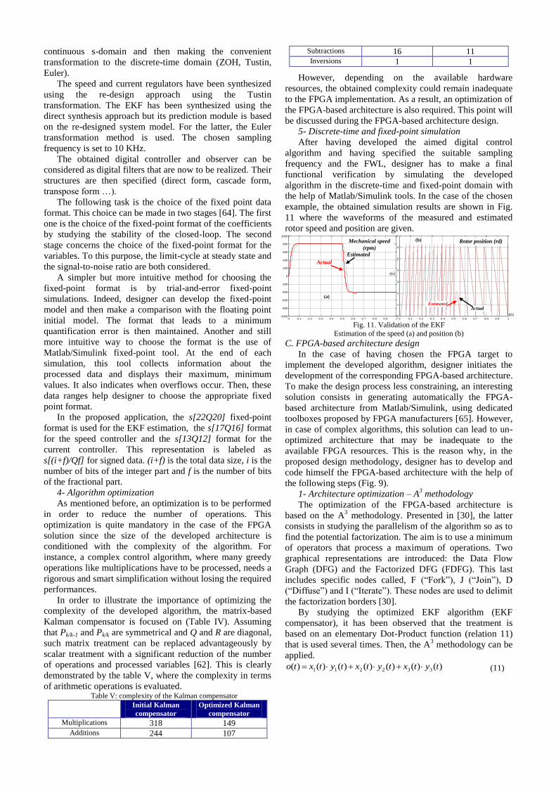
1- Architecture optimization – A3 methodology
The optimization of the FPGA-based architecture is
based on the A3 methodology. Presented in [30], the latter
consists in studying the parallelism of the algorithm so as to
find the potential factorization. The aim is to use a minimum
of operators that process a maximum of operations. Two
graphical representations are introduced: the Data Flow
Graph (DFG) and the Factorized DFG (FDFG). This last
includes specific nodes called, F (“Fork”), J (“Join”), D
(“Diffuse”) and I (“Iterate”). These nodes are used to delimit
the factorization borders [30].
By studying the optimized EKF algorithm (EKF
compensator), it has been observed that the treatment is
based on an elementary Dot-Product function (relation 11)
that is used several times. Then, the A3 methodology can be
applied.
)()()()()()()( 332211 tytxtytxtytxto
0 0.1 0.2 0.3 0.4 0.5 0.6 0.7 0.8 0.9 1-1000
-800
-600
-400
-200
0
200
400
600
800
1000
0 0.1 0.2 0.3 0.4 0.5 0.6 0.7 0.8 0.9 10
1
2
3
4
5
6
7
Mechanical speed
(rpm)
Rotor position (rd)
Estimated
Actual
t(s)
Actual Estimated
t(s)
(a)
(b)
(11)
Fig. 12. Developed DFG and FDFG
Fig. 12(a) shows the DFG of the developed Dot-Product.
The multiplications can be performed in parallel mode
which is not the case of additions. Thus, the factorization
process can be applied to the multiplier operator and the
obtained FDFG is presented in Fig. 12(b). Since this
function is used several times, the EKF compensator can
also be factorized. The obtained FDFG is then presented in
Fig. 13.
Fig. 13. Developed FDFG – Factorization of a thicker grain operator 2- Architecture design
According to the obtained FDFG, the FPGA-based
architecture is designed by replacing the FDFG nodes (F, J
and I) by their corresponding operators. Thus, the node F is
replaced by a multiplexer, J and I replaced by registers. The
hardware architecture of each of the developed modules
(according to the adopted partitioning) is then composed of
a data path and a control unit that are both synchronized
with the global clock signal.
The data path contains the used operators and data buses
between them. The treatment scheduling is ensured by the
control unit which is a simple Finite State Machine (FSM).
The latter is activated via a Start pulse signal. When the
computation time process is over, an End pulse signal
indicates the end of the treatment. As an example, Fig. 14
presents the FPGA architecture corresponding to the FDFG
of Fig. 12(b).
Fig. 14. Example of a designed FPGA architecture
3- Functional simulation
After having developed the VHDL design, the
simulation is started. In our case, ModelSim tools have been
used. The obtained simulation results can also be compared
to those obtained during the Matlab/Simulink environment.
Fig. 15 shows the obtained results for the presented
application.
Fig. 15. Functional validation of the FPGA-based sensorless controller
4- Design synthesis and time/area performances analysis
Once the global FPGA architecture is functionally
validated, the next step is the analysis of the time/area
performances. This is obtained after having synthesized the
developed design (using the dedicated synthesis tools). This
synthesis indicates the consumed FPGA resources and the
maximum frequency of the operating clock. This maximum
frequency allows the calculation of the global execution
time.
Table VI summarizes the obtained synthesis results of
the whole sensorless controller (including the EKF, speed
and currents regulators). From these results, the time/area
performances are extracted. The minimum execution time is
given. All these data are listed for different FPGA device
solutions including low cost and high performance Xilinx
FPGAs. Table VI: Synthesis results for the full FPGA-based sensorless controller
Spartan 3E
xc3s1600E Spartan 6
xc6slx150
Virtex 2P
xc2vp30 Virtex 6
Xc6vsx475
Max. clk
Frequency 54 MHz 97 MHz 167 MHz 253 MHz
Global
resources use
-45% (3688
CLB)
-100% hw 18-bit
multipliers
-5.8% (11519
CLB)
-26 % hw 18-bit DSP
blocks
-39% (3424 CLB)
-38% hw 18-
bit multipliers
-2.5%
(37200 CLB)
-2.5% hw
18-bit DSP blocks
Matlab/Simulink
Speed
Position
ModelSim Matlab/Simulink
ModelSim
ModelSim results
x
+
Sel Sel en0
en0
en0
en0
en2 en1
en3
en0
en1
en2
en3
Clk Reset
Start End
Wait
en0=1 Sel=0
Sel=1
en2=1 Sel=2 Sel=1
en3=1
End=1
Reset
Start
en0
en3
+
en0
en4
Sel=0 en1=1
Sel=2
en4=1
x1 x2 x3
y1 y2 y3
x1
x2
x3 y3
y2
y1
Sel
en4
o
Data-Path
Control unit
Module
architecture
Clk Reset
I
I
I
I
J
J
Dot Product
F
F
F
F
F
F
Fdnk
Pnk-1/k-1
Knk
Pnk/k-1
Pnk/k
x1(t)
y1(t)
x2(t)
y2(t)
x3(t)
y3(t)
x1(t)
y1(t)
x2(t)
y2(t)
x3(t)
y3(t)
o(t)
Matr
ices
ele
men
ts
Matr
ices
ele
men
ts
+
+ Matrix
inversion
11
1/ knkP
12
1/ knkP
21
1/ knkP
22
1/ knkP 11R
22R
o = x1y1+ x2y2+ x3y3 Q
x x
x1
+
b - FDFG
x F F
J
+ F : Fork
J : Join
x
+
y1 x2 y2 x3 y3
o
x1
x2
x3
y1
y2
y3
+ o
a - DFG

tex_min 5,130 µs 3,214 µs 2,873 µs 2,712 µs
D. Experimentation
1- Hardware In the Loop (HIL) validation
In order to verify a first operating attempt, it is highly
recommended to start the experimentation by the HIL
validation. The latter can be considered as an intermediate
between a fully computer-based development validation
(simulation tools and FPGA design tools) and a fully
experimental validation (actual system platform). The HIL
procedure is carried out through a physical implementation
of the developed FPGA-based architecture to be validated.
The latter has to be associated with a real-time emulation of
the plant. In addition, a communication controller has to be
implemented in order to transfer the stimuli and the probed
data. This communication is made with a Host-PC in which
a comparison between the obtained HIL results and the
simulation results is made.
The developed EKF-based sensorless controller has been
implemented and associated with an emulated plant model
(synchronous motor model, VSI model and the mechanical
load model). Fig. 16 highlights the synopsis of the achieved
HIL test.
Fig. 16. HIL procedure
Fig. 17. HIL validation of the EKF estimation
When using a Xilinx FPGA target, the HIL procedure is
made using the ChipScope analyzer [39]. The latter is used
to probe the internal signals in one hand and to configure the
design in the other hand. The data transfer is made using the
JTAG interface. The obtained results are depicted in Fig. 17.
The validation is then made by comparing them to the
simulation results (Fig. 11 and Fig. 15).
2- Experimental validation
The experimental validation has been achieved with the
platform presented in Fig. 18. For experimental constraints,
the used digital control unit is based on a Xilinx XUP
Virtex_2P board. The treatment is synchronized with a 50
MHz clock signal. The total execution time is then equal to
6µs. Fig. 19 presents the waveforms of the speed and
position estimation. These experiments are carried out with
a 800W four poles synchronous machine.
Fig. 18. Prototyping platform
E. System on Chip FPGA design
For benchmarking reasons, we have also implemented
the sensorless controller in software based on the
synthesizable MicroBlaze [39] processor core. The
Peripheral Local Bus (PLB) is used to connect this processor
with the used peripherals (GPIO, timers, PWM, Interrupt
controllers, user-defined data acquisition module…).
This software design is fully carried out using assembly
macros and C-coded functions. To augment the ALU
performances of these functions, the optional “hardware
multiply” and “hardware divide” are included. The EDK
tool automatically generates the memory map of the
hardware platform and assigns default drivers to the
processor and each of its peripherals. The execution routine
of the proposed algorithm is depicted in Fig. 20.
The MicroBlaze is synchronized with a 100 MHz clock
and the sampling period (interruption cycle) is set to 100 µs.
The execution time of the whole sensorless controller has
been evaluated to 85µs. The surface occupation of the
design is 11 % of the used Virtex 5 XC5VLX50T FPGA.
Note that external 12-bit ADCs are used for data acquisition.
In order to make a comparison to a standard software
solution, the same sensorless controller has been
implemented in a TI TMSF2808 DSP device (100MHz,
32Bit, 12-bit ADC, 2x16-bit multiplier, 16Ko RAM
memory, [63]). The same execution routine is preserved and
the total execution time has been evaluated to 66 µs [61].
The functions are fully C-coded. One can stress from the
obtained timing results that standard software devices
remain more adapted for a full software implementation.
This is mainly due to the design tools that are more mature.
Ts= TPWM= 100µs
Pro
gra
m
Inte
rru
pti
on
PWM signals generation
(1) (2) (3) (4) (5)
t
t
Tex (2) EKF state space estimation process
(3) P-PI speed controller
(4) PI current controller
(5) PWM process
PWM carrier
k.Ts (k+1).Ts
Fig. 20. Timing diagram - case of a full
software sensorless controller
(1) (2) (3) (4) (5)
Data acquisition (ADC)
500 rpm
0 rpm
Actual
Estimated
Estimated
Actual
(a)
(b)
Fig. 19. Experimental results – waveforms of the estimated
speed (a) and rotor position (b)
Actual
Estimated
Emulated physical
plant
FPGA- based sensorless
controller
Com. Controller Stimuli Signal Probe
Com. Interface
Host-PC
Comparison
Simulation
results
HIL
results
FP
GA
target
Current & voltage Sensors
Synchronous
machine
Load
FPGA board 3φ rectifier
+ VSI Module ADC board
The way of coding and the quality of the compilation tools
are also determinant points.
For these reasons and in order to benefit from the
flexibility of SoC approaches and the high control
performances achievable with hardware designs, it is
interesting to combine both software and hardware
treatments. For this aim, it is highly recommended to adopt
co-design methodologies so as to make an intelligent
partitioning between the software treatment and the
hardware treatment.
IV- FPGA CONTROLLERS BASED ON ARTIFICIAL
INTELLIGENCE
Traditionally, mathematical models were developed to
evaluate the functionality of global engineering systems.
However, the practical development of each part of the
system needs then to be separately addressed. This often
involves the use of different software platforms, the design
itself being developed in a different environment. Recent
advances in CAD tools have brought the functional
description of design and practical hardware implementation
closer.
The use of modern Electronic Design Automation
packages for electronic systems design facilitates easy
implementation of complex control algorithms and Artificial
Intelligence (AI) into hardware. Hence, a wide range of
complex and intelligent controller designs have been
recently developed, with applications in industry [66-70]. A
significant number of them target FPGAs, due to the rapid
prototyping features and the flexibility offered by FPGAs,
especially through the recent availability of microprocessor
or DSP cores, allowing hardware software co-design and
implementation [71].
A relevant paper in this context deals with custom
architectures for Fuzzy and Neural Networks controllers
[72]. It presents efficient architecture approaches to develop
controllers using specific circuits, using HDLs and
synthesizing them to get the FPGA configuration bit-stream.
Some more specific areas using FPGAs for the
implementation of complex controllers based on Artificial
Intelligence are highlighted below.
A. Neural Networks implemented in FPGA
According to an European Network of Excellence (ENE)
report [73], the future implementation of hardware neural
networks is shaped in 3 ways: i) by developing advanced
techniques for mapping neural networks onto FPGA, ii) by
developing innovative learning algorithms which are
hardware-realizable, iii) by defining high-level descriptions
of the neural algorithms in an industry standard to allow full
simulations and fabrication and to produce demonstrators of
the technology for industry. Such new designs will be of use
to industry if the cost of adopting them is sufficiently low.
Hardware-based neural networks are important to industry
as they offer low power consumption and small size
compared to PC software and they can be embedded in a
wide range of systems. Software libraries exist for
traditional Artificial Neural Network (ANN) models
(Matlab). The industry-standard form is however
VHDL/Verilog or C++ parameterized modular code,
allowing customization.
A wide range of research papers on Neural Networks
based Controllers were published in prestigious journals.
Some were collated in special issues on Transactions of
Industrial Electronics [74, 75].
An interesting trend, which confirms the ENE report [73], is
given by the recent development and implementation results
of a parameterized FPGA-based architecture for feed-
forward multi layer perceptrons with backpropagation
learning algorithm (FF-MLPs) presented in [76]. The
proposed architecture makes possible native prototyping and
design space exploration in hardware.
Others papers [77,78] exploit the learn ability of ANNs.
Paper [76] presents an adaptive low-speed-damping
controller for a stepper motor which removes nonlinear
disturbance at low speeds and paper [78] shows a self-tuning
PID FPGA-based motion controller using RBF NN for a X-
Y table.
B. Fuzzy Logic Based Control Systems
Today, fuzzy logic based control systems, or simply,
Fuzzy Logic Controllers (FLCs) can be found in a growing
number of products, from washing machines to speedboats,
from air condition units to hand-held autofocus cameras.
The success of fuzzy logic controllers is mainly due to their
ability to cope with knowledge represented in a linguistic
form instead of representation in the conventional
mathematical framework. Control engineers have
traditionally relied on mathematical models for their
designs. However, the more complex a system, the less
effective the mathematical model.
FPGAs constitute an appropriate target for the
implementation of fuzzy-logic controllers, facilitated by the
flexibility of the design environment, enabling direct
implementation of the circuit’s abstract model. A high
number of works have been published on fuzzy logic-based
control systems. One paper presents a method employing
hardware/software co-design techniques according to an ‘a
priori’ partition of the tasks assigned to the selected
components. This feature makes it possible to tackle the
control system prototyping as one of the design stages. In
this case, the platform considered for prototyping has been a
development board containing a standard microcontroller
and an FPGA. Experimental results from an actual control
application validate the efficiency of this methodology [79].
A paper, advocates a novel approach to implement the
fuzzy logic controller for speed control of electric vehicle by
using FPGA [80]. Another paper [81] presents an
implementation of a FLC on a reconfigurable FPGA system,
while a different paper explores the use of FPGA
technologies to implement FLCs. Two different approaches
are described. The first option is based on the logic synthesis
of the boolean equations describing the controller input-
output relations. The second approach uses dedicated
hardware to implement the fuzzy algorithm according to a
specific architecture based on a VHDL cell library [82]. A
FPGA based fuzzy sliding-mode controller, which combines
both the merits of fuzzy control and sliding-mode control, is
proposed in [83], to control the mover position of a linear
induction motor (LIM) drive to compensate the uncertainties
including the frictional force.
Paper [84] presents an H-bridge multilevel converter
governed by an integrated fuzzy logic controller/modulator
designed with VHDL and implemented in FPGA.
A design environment for the synthesis of embedded FLC
on FPGAs, which provides a novel implementation
technique has been developed in [85]. It allows accelerating
the exploration of the design space of fuzzy control
modules, as well as a codesign flow that eases their
integration into complex control systems. Even an FLC
based ant colony optimization (ACO) application has been
proposed in [86] for improving designs efficiency and
control performance, as well as ACO hardware
implementation.
C. Intelligent Data Acquisition Devices (DAQ)
Intelligent DAQ devices use National Instruments (NI)
LabVIEW reconfigurable FPGAs to implement custom
high-performance data acquisition on commercial off-the-
shelf (COTS) hardware. Instead of a predefined subset of
DAQ functionality, the intelligent DAQ uses an FPGA-
based system timing controller to make all analog and
digital I/Os configurable for application-specific operation.
By programming the FPGA, the custom high-performance
DAQ tasks can easily be implemented. Additionally,
because of the parallel architectures of FPGAs, the high-
performance task implementation is achieved without
performance degradation [87]. DMA provides a direct link
for data on the FPGA to RAM on the host machine,
improving data-logging efficiency and making data
immediately available for analysis and visualization. This
high-speed data transfer provides real-time visibility into
parameters and variables within the FPGA.
Furthermore, adding an FPGA circuit to a DAQ platform
interfaced by the NI Labview graphical system design tool
gives the ability to perform early signal pre-processing and
offers new valuable abilities like reconfigurability – first
step towards a self reconfigurable device ready to respond in
real time to any external or intrinsic changes [88]. On the
other hand, Labview may be used as a graphical
programming environment for FPGA targeted designs. The
new LabVIEW FPGA environment enables application
domain experts without prior knowledge of hardware
description languages (HDLs) to program reconfigurable
hardware devices. Such method is used in paper [89],
illustrating how LabVIEW FPGA supports a flexible,
reliable and cost-effective hardware design considering an
ultra-high speed control application with complex timing
synchronization. Other applications may be found in paper
[90], in which an isolated wind energy conversion system
based on the cascaded H-bridge multilevel inverter topology
is considered or paper [91] which presents a high frequency
radars controller designed in NI LabVIEW FPGA or even
space applications as in paper [92]. A powerful combination
of the parallel signal processing using neural networks
implemented in FPGA with Labview as interface for an
intelligent DAQ can be found in paper [93]. The output is an
implementation of a neural network based estimator of the
load machine speed for two-mass drive system on FPGA.
D. Evolvable hardware
Evolvable hardware offers much for the future of
complex system design. Evolutionary techniques not only
give the potential to explore larger solution spaces, but when
implemented on hardware allow system designs to adapt to
changes in the environment, including failures in system
components. Evolutionary algorithms have been developed
and applied to intrinsic hardware evolution, aiming to
produce an evolutionary system that can be readily
implemented on COTS hardware. An FPGA-based
controller for a mobile robot has been developed by Prof.
Andy Tyrrell and his team at University of York, UK. The
controller consists of look-up tables, which perform the
mapping from sensor data to actuator, evolved using an
effective evolutionary algorithm [94]. Paper [95] presents
how a self-generated architecture may be used to build-up a
secret physical cipher unit with dynamic security properties.
Another application can be found in [96], where a run-time
adaptable evolvable hardware classifier system is proposed
or in [97], in which a FPGA based customizable general-
purpose GA engine has been reported. A novel bio-inspired
self-test technique for the implementation of evolvable fault
tolerant systems, which mimics a Unitronic (unicellular
electronic) artificial system, is presented in [98]. The system
is implemented in FPGA like a bio-inspired cellular array
and made up of structurally identical cells with self-
diagnostic and self-healing capability.
V- NEURAL NETWORK BASED FPGA SYSTEMS –
CASE STUDIES
Artificial Neural Networks (ANNs) are also an
interesting research field where FPGAs have been
successfully used. Many recent publications ([9], [99],
[100], [101]) consider the FPGA as an effective
implementation solution of control algorithms for industrial
applications. Hardware implemented ANNs have an
important advantage over computer simulated ones by fully
exploiting the parallel operation of the neurones, thereby
achieving high speed of information processing.
A. Case study 1: FPGA NN Hardware Implementation
Algorithm
Some VLSI algorithms achieve efficient NN
implementation. An algorithm for compact neural network
hardware implementation, by using a combination of AND
gates, OR gates and Threshold Gates (TG), leads to compact
hardware structures. However, it cannot be used for direct
FPGA implementation because TGs are not available in
FPGA logic cells [102]. In order to minimize both ASIC and
FPGA hardware implementation of ANNs composed of
neurones with step activation functions, the solution is to
treat each neurone as a Boolean function and to implement it
separately. This leads to minimize the implementation
complexity. The most useful property of such a Boolean
function is that if its truth table is constructed as a matrix
with as many dimensions as neurone inputs, then the truth
table has only one large group of ‘1’ and one large group of
‘0’. The solid group of ‘1’ is not visible when the Gray
codification is used and thus classical Quine-McClusky
algorithms or Karnaugh maps cannot efficiently be used.
The proposed algorithm [103] uses a different approach and
generates a multilayer pyramidal hardware structure, where
layers of AND gates alternate with layers of OR gates. The
bottom layer consists of incomplete NOT gates, a structure
to be optimised later by eliminating redundant logic gates
groups. However, the method is effective only when the numbers
of inputs and bits on each input are low, otherwise a
classical circuit may be more efficient. The algorithm itself
contains three steps: ANN mathematical model digitisation,
conversion of the digitised model into a logic gate structure,
and hardware optimisation by elimination of redundant logic
gates. A set of C++ programs automates algorithm
implementation, generating optimised VHDL code. This
strategy bridges the gap between ANN design software and
hardware design packages (Xilinx). Although the method is
directly applicable only to neurones with step activation
functions, it can be extended to sigmoidal functions.
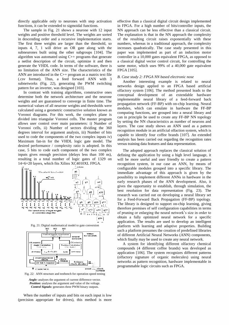
The sample in Fig. 21 shows a neurone with 12 input
weights and positive threshold level. The weights are sorted
in descending order and a recursive implementation starts.
The first three weights are larger than the threshold, so
inputs 4, 7, 1 will drive an OR gate along with the
subneurones built using the other subgroups [104]. The
algorithm was automated using C++ programs that generate
a netlist description of the circuit, optimize it and then
generate the VHDL code. In terms of the software, there is
no limitation of the ANN size. The characteristics of the
ANN are introduced in the C++ program as a matrix text file
(.csv format). Thus, a feed forward ANN with 3
subnetworks (Fig. 22), generating the PWM switching
pattern for an inverter, was designed [103].
In contrast with training algorithms, constructive ones
determine both the network architecture and the neurone
weights and are guaranteed to converge in finite time. The
numerical values of all neurone weights and thresholds were
calculated using a geometric constructive solution known as
Voronoi diagrams. For this work, the complex plane is
divided into triangular Voronoi cells. The master program
allows user control over main parameters: i) Number of
Voronoi cells, ii) Number of sectors dividing the 360
degrees interval for argument analysis, iii) Number of bits
used to code the components of the two complex inputs iv)
Maximum fan-in for the VHDL logic gate model. The
desired performance / complexity ratio is adopted. In this
case, 5 bits to code each component of the two complex
inputs gives enough precision (delays less than 100 ns),
resulting in a total number of logic gates of 1329 on
14+6=20 layers, which fits Xilinx XC4010XL FPGA.
Fig. 21: Digital mathematical model to gate conversion
Fig. 22: ANN structure and testbench for operation speed testing
Angle: analyses the argument of current difference vector.
Position: analyses the argument and value of the voltage. Control Signals: generates three PWM binary outputs.
When the number of inputs and bits on each input is low
(precision appropriate for drives), this method is more
effective than a classical digital circuit design implemented
in FPGA. For a high number of bits/controller inputs, the
NN approach can be less effective than a classical circuit.
The explanation is that in the NN approach the complexity
of the resulting circuit raises exponentially with these
numbers, whereas in a traditional approach, the complexity
increases quadratically. The case study presented in this
paper was implemented as part of an induction motor
controller in a 10,000 gates equivalent FPGA, as opposed to
a classical digital vector control circuit, for controlling the
same motor, which uses 99% of a 40,000 gate equivalent
FPGA [105].
B. Case study 2: FPGA NN based electronic nose
Another interesting example is related to neural
networks design applied to an FPGA based artificial
olfactory system [106]. The method presented leads to the
conceptual development of an extendable hardware
implementable neural library of a feed-forward back
propagation network (FF-BP) with on-chip learning. Neural
modules, which can emulate in hardware the FF-BP
computing functions, are grouped into a neural library and
can in principle be used to create any FF-BP NN topology
by setting the NN characteristics as number of neurons and
layers. The case study shows an ANN used as a pattern
recognition module in an artificial olfaction system, which is
capable to identify four coffee brands [107]. An extended
analysis has been carried out regarding the recognition rates
versus training data features and data representation.
The adopted approach replaces the classical solution of
defining the application by using a high level language, it
will be more useful and user friendly to create a pattern
recognition system, in our case an ANN, by means of
configurable modules grouped into a specific library. The
immediate advantage of this approach is given by the
possibility to implement different ANNs in hardware in the
early research phases of the ANN development. Also, it
gives the opportunity to establish, through simulation, the
best resolution for data representation (Fig. 23). The
research was carried out on developing a neural library set
for a Feed-Forward Back Propagation (FF-BP) topology.
The library is designed to support on-chip learning, giving
therefore premises of self configuration capabilities in terms
of pruning or enlarging the neural network’s size in order to
obtain a fully optimized neural network for a specific
application. The results are used to develop an intelligent
platform with learning and adaptive properties. Building
such a platform presumes the creation of predefined libraries
of different Artificial Neural Networks (ANN) components,
which finally may be used to create any neural network.
A system for identifying different olfactory chemical
compounds (4 different coffee brands) was developed as
application [106]. The system recognizes different patterns
(olfactory signature of organic molecules) using neural
networks as pattern recognition, hardware implementable in
programmable logic circuits such as FPGA.

Fig. 23. Proposed method for hardware implemented ANN design
Discovering the optimal topology of an ANN for a
particular application remains an important issue, especially
for highly competent classifiers such as FF-BP neural
networks. It most cases, so far, the appropriate choice of the
network features, the training methodology to be used, and
the best network topology have been identified by repetitive
simulations and modifications of the project code.
Therefore, a library with ANN components, ready to be
hardware implemented, represents a step forward towards a
more user friendly design environment. An extendable
hardware implementable neural library has been developed,
considering a FF-BP network topology with on-chip
learning. The implementation goal is achieved using the
Mathworks’ Simulink environment for functional
specification and System Generation, to generate the VHDL
code according to the chosen FPGA device features.
In order to discuss the functions that have to be
implemented, it is important to specify the architecture of
the MLP networks: the neurons are organized in at least 3
layers: one input layer, one output layer and one or more
intermediate, hidden layers. The network is fully connected,
i.e. all the outputs of a layer are connected by synapses to all
inputs of the following layer. Only the hidden and the output
layers include processing units, whereas the input layer is
used just for data feeding. The parallelism adopted is a node
one and requires managing all the neurons from the same
layer at the same time. Therefore, the control blocks that
command the behaviour of the neuron elements are common
for all neurons of a layer.
Another main component of the artificial neuron, and
usually a bottleneck for its speed performance, is the
sigmoid activation function. Its hardware implementation
implies important hardware resource utilization [108]. In
order to reduce such consumption is useful to adopt different
approximations (depending of the available hardware
resources) with minimum errors. The principal classical
methods to digitally implement an activation function are
Look-up tables and truncation of the Taylor series
expansion. Also, there are approximations with smaller
errors, but they use floating-point multiplications, thus a
practical VLSI implementation becomes far too complicated
[109, 110].
In order to create the library modules of the sigmoid
firing function, using System Generator/Simulink blocks,
hardware implementations for the following approximation
functions have been produced. The implementation reports
conclude that that the best approximation method is the
PLAN function, when the number of the neurons that use
sigmoid function as fire function is larger than the number
of the BRAM blocks available in the FPGA circuit. When
the number of neurons is lower than the total BRAM blocks
available in the FPGA circuit, the best way to approximate
the sigmoid function is the Lookup Tables method.
The process parallelism adopted implies that all the
neurons within the same layer are controlled at the same
time. The blocks are described using VHDL language and
implemented using a block that converts a VHDL design
into a System Generator/Simulink block. The computation
results show that the largest NN which can be implemented
into the 4VSX35 circuit is a FF-BP neural network with
maximum of 120 neurons distributed as: 80 in the hidden
layer and 40 in the output layer.
The FF-BP neural network design environment
developed was used to create a pattern recognition module
for an artificial olfactory system capable to recognize
different types of coffee. The olfactory system consists of
(Fig. 24):
- seven gas sensors chosen to react to a wide spectrum of
odours (TGS842, TGS826_1, TGS826_2, TGS2600,
TGS2601, TGS2602, TGS2620),
- temperature sensor (LM35),
- humidity sensor (SY-HS-230) - (all sensors are mounted
into a gas test chamber),
- test chamber,
- three pumps for gas carrying,
- circuits for sensors conditioning and pumps command,
- data acquisition board (PCI-MIO-16E-1),
- pattern recognizing module hardware implemented in
FPGA (Virtex-4 SX MB - 4VSX35),
- user interface developed in Labview 8.2.
The data acquisition module was created in Labview
environment using a virtual instrument (VI) customized to
execute the following tasks: to acquire data generated by all
9 sensors, to pre-process the acquisitioned signals (filtering,
drift cancellation) and to save data as text file format (.lvm
file). Therefore, the modules that compound the VI consist
of: pumps control module, data acquisition control module,
sub-VIs control time module, pre-processing signal module,
C grade conversion module of the signal generated by the
temperature sensor and %RH conversion module of the
signal generated by the humidity sensor.
Fig. 24. The architecture of the adopted artificial olfaction system

The data has been extracted using the scenario presented
in Fig. 25. It roughly comprises three processes. The first is
the baseline calculation (the average voltage drop on sensors
resistance when the reference gas, air, is applied). The
second and third stages presume measurement with a fixed
sampled frequency over a defined time, absorption and
respectively desorption time, of the voltage drop on sensors
resistance when the enriched odour is applied. A regular
absorption / desorption operation, which presents the results
of time settings vs. voltage drop on sensor resistor is shown
in Fig. 25.
To conclude the second case study presented, it can be
stated that a novel neural design strategy has been
developed, which benefits of reduced design time over
classical field orientation approaches, leading to a low
complexity and easy to implement pattern recognition
module. A particular application of the pattern recognition
system for an olfactory system was investigated and results
presented show efficient hardware implementation in FPGA
circuit. The neural network used as pattern recognition
system was designed using a hardware-software co-design
environment, in a manner that facilitates control over the
hardware implementation complexity, and was downloaded
into a Xilinx FPGA circuit.
The achievement presented in this case study refers to a
holistic modelling/design method, using modules created
into hardware-software co-design environment (Matlab-
System Generator–ISE) and grouped in a specific NN
library. These modules emulate in hardware any FF-BP
network topology behaviour, giving the opportunity to design
hardware implementable FF-BP neural networks, at a higher
level. As a specific application, a FF-BP network has been
used as pattern recognition module for an artificial olfactory
system, capable to recognize 4 coffee types. Also, the
influence over the recognition rates of data representation
resolution and data training dimensionality has been
analysed. The observations have been used to determine the
neural network which has the best recognition rates with
minimum hardware resource utilization.
V- CONCLUSIONS AND FUTURE TRENDS
The aim of this paper was to present the FPGA
technologies and highlight their use in industrial control
applications. It has been underlined that these hardware
solutions can perfectly address the nowadays challenges in
this field such as high control performances, low cost,
reliability, power consumption and immunity to radiations.
The contribution of these hardware devices was then
discussed. The case of embedded systems, and industrial
control systems were focused on. For the embedded
systems, it has been stated that FPGAs are becoming an
interesting option in many applications like robotics,
networking, automotive and aircraft. Indeed, FPGAs are
bringing many benefits in terms of safety, rapidity and
power consumption.
In the case of control applications, It has been shown
that FPGA-based controller can be an efficient option for
both the high demanding applications and the constrained
switching frequency applications. The first group
corresponds to high switching frequency applications, high
level of parallelism applications and HIL applications.
Regarding the second group for which the switching
frequency is limited, it has been shown that we can take
advantage of the rapidity of FPGAs to boost the
performances of the controller.
Authors have firstly made a generic presentation of the
FPGAs. Their internal structure and their configuration
technologies were described. A discussion about the design
tools was also made.
In the industrial control domain, the control algorithms
become more and more complex. To illustrate the interest of
FPGAs in such complex controller, authors have presented
an example of application which consists of a sensorless
motor controller. To estimate the rotor position and the
speed of the used synchronous machine, an Extended
Kalman Filter was used. The development of the FPGA-
based sensorless controller was then made according to a
design methodology which is required especially for such
complex algorithms.
Another relevant field which was discussed is the Neural
Network (NN) systems. The use of FPGAs in such
applications is highly interesting since the parallelism of the
NN algorithms is preserved. For an illustration purpose,
authors have resented case studies.
In the near future, the complexity of the digital control
systems will continue to grow and the tasks devoted to the
control algorithm will no longer be limited to regulation but
have to manage EMI, communications, health monitoring,
diagnosis and fault-adaptive on line control. As a
consequence and from an algorithm point of view, signal
processing functions for power applications will be the
center of intensive researches. From this perspective, FPGA-
based controller represents a very attractive solution too.
Finally, we shall end by shortly introducing the main
challenges in terms of architecture, this aspect being closely
related to the algorithm and at the same time offers in itself
a degree of creativity. Among the most exciting trends we
can quote the introduction of the floating point computing
evaluation for FPGA-based solutions. What is its cost in
terms of hardware resources? Is it necessary for industrial
control applications where the dynamic range of variables
and the complexity of the control algorithm are still limited?
Another interesting field of research is the co-design
approach, with questions like how to make an optimized
partitioning between the software part of the controller
architecture and its hardware part?, [111]. Another issue
concerns mixed integration. Indeed, as seen before and due
to their rapidity FPGA-based controllers are now
introducing only a small delay in the loop and because of
their high density rate can easily work with a high accuracy
(high number of bits). This makes the controller quasi-
transparent moving the limitations of time and accuracy
towards the interfaces like ADCs and the drivers.
Another challenging point is the system integration.
Indeed, in embedded systems (e.g. aircraft, space,
automotive) the surface occupation of the systems is a key
issue. To this purpose, it is advantageous to used digital
Fig. 25. Voltage variation with baseline time, baseline calculation time,
absorption time and desorption time
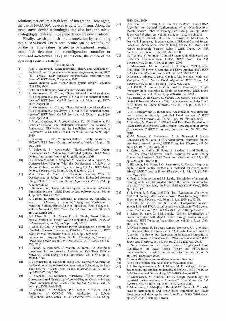
solutions that ensure a high level of integration. Here again,
the use of FPGA SoC devices is quite promising. Along the
trend, novel device technologies that also integrate mixed
analog/digital features in the same device are now available.
Finally, we shall finish this enumeration by reminding
that SRAM-based FPGA architecture can be reconfigured
on the fly. This feature has also to be explored having in
mind fault detection and reconfiguration controller or
optimized architecture [112]. In this case, the choice of the
operating system is crucial.
REFERENCES [1] Ajay V Deshmukh, “Microcontrollers, Theory and Applications”,
the MacGraw-Hill companies, Computer Engineering series, 2007
[2] Phil Lapsley, “DSP processor fundamentals: architecture and features”, IEEE Press, Computers, 1997
[3] Wayne Hendrix Wolf, “FPGA-based system design”, Prentice
Hall PTR, 2004 [4] Actel on-line literature. Available in www.actel.com
[5] E. Monmasson, M. Cirstea, “Guest Editorial special section on
field programmable gate arrays (FPGAs) used in industrial control systems”, IEEE Trans. On Ind. Electron., vol. 54, no. 4, pp. 1807–
1809, August 2007
[6] E. Monmasson, M. Cirstea, “Guest Editorial special section on field programmable gate arrays (FPGAs) used in industrial control
systems”, IEEE Trans. On Ind. Electron., vol. 55, no. 4, pp. 1499–
1500, April 2008 [7] J. Munoz-Castaner, R. Asorey-Cacheda, F.J. Gil-Castineira, F.J.
Gonzalez-Castano, P.S. Rodriguez-Hernandez, “A Review of
Aeronautical Electronics and its Parallelism with Automotive Electronics”, IEEE Trans. On Ind. Electron., vol. 54, no. 99, April
2010
[8] P. Conmy, I. Bate, “Component-Based Safety Analysis of FPGAs”, IEEE Trans. On Ind. Informatics, Vol.6, n° 2, pp. 195,
May 2010
[9] F. Salewski, S. Kowalewski, “Hardware/Software Design Considerations for Automotive Embedded Systems”, IEEE Trans.
On Ind. Informatics, Vol. 4, n° 3, pp. 56, August 2008
[10] H. Guzman-Miranda, L. Sterpone, M. Violante, M.A. Aguirre, M. Gutierrez-Rizo, “Coping With the Obsolescence of Safety- or
Mission-Critical Embedded Systems Using FPGAs”, IEEE Trans.
On Ind. Electron., vol. 58, no. 3, pp. 814, Marsh 2011 [11] M.A. Gora, A. Maiti, P. Schaumont, “Coping With the
Obsolescence of Safety- or Mission-Critical Embedded Systems
Using FPGAs”, IEEE Trans. On Ind. Informatics, Vol. 6, n° 4, pp. 719, Nov. 2010
[12] F. Simonot-Lion, "Guest Editorial Special Section on In-Vehicle
Embedded Systems", IEEE Trans. on Ind. Informatics, vol. 56, no. 4, pp. 372 - 374, Oct 2009.
[13] F. Baronti, E. Petri, S. Saponara, L. Fanucci, R. Roncella, R.
Saletti, P. D'Abramo, R. Serventi, “Design and Verification of Hardware Building Blocks for High-Speed and Fault-Tolerant In-
Vehicle Networks”, IEEE Trans. On Ind. Electron., vol. 58, no. 3,
pp. 792, Marsh 2011 [14] J.-J. Chen, X. S. Hu, Mossé, D. , L. Thiele, "Guest Editorial
Special Section on Power-Aware Computing ," IEEE Trans. on
Ind. Informatics, vol. 57, no. 3, pp. , July 2010. [15] J. Choi, H. Cha, "A Processor Power Management Scheme for
Handheld Systems Considering Off-Chip Contributions ," IEEE
Trans. on Ind. Informatics, vol. 57, no. 3, pp. , Jyly 2010. [16] Fuming Sun, Haiyang Wang, Fei Fu, Xiaoying Li, “Survey of
FPGA low power design”, In Proc. ICICIP’2010 Conf., pp. 547-
550, 2010 [17] P. Ferrari, A. Flammini, D. Marioli, A. Taroni, “A Distributed
Instrument for Performance Analysis of Real-Time Ethernet Networks”, IEEE Trans. On Ind. Informatics, Vol. 4, N° 1, pp. 16-
25, Feb. 2008
[18] S. Fischmeister, R. Trausmuth, Insup Lee, "Hardware Acceleration for Conditional State-Based Communication Scheduling on Real-
Time Ethernet ," IEEE Trans. on Ind. Informatics, vol. 56, no. 3,
pp. 325 - 337, July 2009. [19] L. Vachhani, K. Sridharan, “Hardware-Efficient Prediction-
Correction-Based Generalized-Voronoi-Diagram Construction and
FPGA Implementation”, IEEE Trans. On Ind. Electron., vol. 55, no. 4, pp. 1558, April 2008
[20] L. Vachhani, K. Sridharan, P.K. Meher, “Efficient FPGA
Realization of CORDIC With Application to Robotic Exploration”, IEEE Trans. On Ind. Electron., vol. 56, no. 12, pp.
4915, Dec. 2009
[21] C.-C. Tsai, H.-C. Huang, S.-C. Lin, “FPGA-Based Parallel DNA
Algorithm for Optimal Configurations of an Omnidirectional Mobile Service Robot Performing Fire Extinguishment”, IEEE
Trans. On Ind. Electron., vol. 58, no. 3, pp. 1016, March 2011
[22] H. Tanaka, K. Ohnishi, H. Nishi, T. Kawai, Y. Morikawa, S. Ozawa, T. Furukawa, “Implementation of Bilateral Control System
Based on Acceleration Control Using FPGA for Multi-DOF
Haptic Endoscopic Surgery Robot”, IEEE Trans. On Ind. Electron., vol. 56, no. 3, pp. 618, March 2009
[23] Li. Tianjian, Y. Fujimoto, “Control System With High-Speed and
Real-Time Communication Links”, IEEE Trans. On Ind. Electron., vol. 55, no. 4, pp. 1548, April 2008
[24] E. Monmasson, M. W. Naouar, L. Idkhajine, “FPGA-based
Controllers for Power Electronics and Drive Applications”, IEEE Ind. Electron. Magazine, vol. 5, n°1, pp. 1-13, March 2011
[25] O. Lopez,, J. Alvarez, J. Doval-Gandoy, F.D. Freijedo, “Multilevel
Multiphase Space Vector PWM Algorithm” IEEE Trans. Ind. Electron., vol. 55, no 5, pp 1933 – 1942, May 2008.
[26] B. J. Patella, A. Prodic, A. Zirger, and D. Maksimovic, “High-
frequency digital controller IC for dc–dc converters,” IEEE Trans. Power Electron., vol. 18, no. 1, pp. 438–446, Jan. 2003.
[27] S.C. Huerta, A. de Castro, O. Garcia, J.A. Cobos, “FPGA-Based
Digital Pulsewidth Modulator With Time Resolution Under 2 ns”, IEEE Trans. on Power Electron., vol. 23, n°6, pp. 3135-3141,
Nov. 2008.
[28] A. V. Peterchev and S. R. Sanders, “Quantization resolution and limit cycling in digitally controlled PWM converters,” IEEE
Trans. Power Electron., vol. 18, no. 1, pp. 301–308, Jan. 2003.
[29] A. Myaing, V. Dinavahi, “FPGA-Based Real-Time Emulation of Power Electronic Systems With Detailed Representation of Device
Characteristics,” IEEE Trans. Ind. Electron., vol. 58, N°1, Dec.
2010. [30] M.-W. Naouar, E. Monmasson, A. A. Naassani, I. Slama-
Belkhodja and N. Patin, “FPGA-based current controllers for AC
machine drives—A review,” IEEE Trans. Ind. Electron., vol. 54, no. 4, pp. 1907–1925, Aug. 2007
[31] S. Karimi, A. Gaillard,P. Poure, S. Saadate, S. “FPGA-Based
Real-Time Power Converter Failure Diagnosis for Wind Energy Conversion Systems,” IEEE Trans. Ind. Electron., vol. 55, n°12,
pp. 4299-4308, Dec. 2008 [32] F. Blaabjerg, P.C. Kjaer, P.O. Rasmussen, C. Cossar, “Improved
digital current control methods in switched reluctance motor
drives,” IEEE Trans. on Power Electron., vol. 14, n°3, pp. 563-572, May 1999.
[33] K. Tazi, E. Monmasson and J.P. Louis, “Description of an entirely
reconfigurable architecture dedicated to the current vector control of a set of AC machines,” In Proc. IEEE-IECON’99 Conf., 1999,
pp. 1415-1420.
[34] Y.-S. Kung, R.-F. Fung, and T.-Y. Tai, “Realization of a motion control IC for x-y table based on novel FPGA technology,” IEEE
Trans. on Ind. Electron., vol. 56, no. 1, Jan. 2009, pp. 43–53.
[35] A. Fratta, G. Griffero, and S. Nieddu, “Comparative analysis among DSP and FPGA-based control capabilities in PWM power
converters,” in Proc. IEEE IECON’04 Conf., 2004, pp.257-262.
[36] B. Miao, R. Zane, D. Maksimovic, “System identification of power converters with digital control through cross-correlation
methods,” IEEE Trans. on Power Electron., vol. 20, n°5, pp. 1093-
109, Sept. 2005. [37] A. Ordaz-Moreno, R. De Jesus Romero-Troncoso, J.A. Vite-Frias,
J.R. Rivera-Gillen, A. Garcia-Perez, “Automatic Online Diagnosis
Algorithm for Broken-Bar Detection on Induction Motors Based on Discret Wavelet Transform for FPGA Implementation,” IEEE
Trans. Ind. Electron., vol. 55, n°5, pp. 2193-2202, May 2008.
[38] P. Simi Valsan and K. Shanti Swarup, “High-Speed Fault Classification in Power Lines: Theory and FPGA-Based
Implementation, ” IEEE Trans. on Ind. Electron., vol. 56, no. 5,
pp. 1793–1800, May 2009. [39] Xilinx on-line literature. Available in www.xilinx.com
[40] Altera on-line literature. Available in www.altera.com
[41] J. J. Rodriguez-Andina, M. J. Moure, M. D. Valdes, “Features, design tools, and application domains of FPGAs”, IEEE Trans. On
Ind. Electron., vol. 54, no. 4, pp. 1810–1823, August 2007.
[42] E. Monmasson, M. Cirstea, “FPGA design methodology for industrial control systems – A review,” IEEE Trans. On Ind.
Electron., vol. 54, no. 4, pp. 1824–1842, August 2007.
[43] E. Monmasson, L. Idkhajine, I. Bahri, M.W. Naouar, L. Charaabi, “Design methodology and FPGA-based controllers for Power
Electronics and drive applications”, In Proc. ICIEA’2010 Conf.,
pp. 2328-2338, Taichung, Taiwan.
[44] L.Idkhajine, E. Monmasson, M-W. Naouar, A.Prata and
K.Bouallaga, “Fully integrated FPGA-based controller for
synchronous motor drives," IEEE Trans. Ind. Electron., vol. 56, n°. 10, pp. 4006-4017, Oct. 2009.
[45] K. Eshraghian, “SoC Emerging Technologies”, IEEE Proceedings,
vol. 94, no. 6, Jun. 2006, pp. 1197 – 1213. [46] G. Martin, “Overview of the MPSoC Design Challenge". in Proc.
DAC’06 Conf., 2006, CD-ROM.
[47] R. Obermaisser, P. Gutwenger,“Model-Based Development of MPSoCs with Support for Early Validation”, in Proc. IEEE
IECON’09 Conf., 2009, CD-ROM.
[48] R. Kumar, D.Tullsen, and N.Jouppi. «Core Architecture Optimization for Heterogeneous Chip Multiprocessors". In Proc.
PACT’2006 Conf., Seattle, April 2006
[49] M. Youssef, S. Yoo, A. Sasongko, Y. Paviot, A. A. Jerraya, “Debugging HW/SW Interface for MPSoC: Video Encoder
System Design Case Study”, In Proc. DAC’04 Conf., 2004, CD-
ROM. [50] C. A. Zeferino, M. E. Kreutz, L. Carro, and A. A. Susin. “A study
on communication issues for systems-on-chip,” In Proc. SBCCI
Conf., 2002, pp. 121–126. [51] A. Brinkmann, J. Niemann, I. Hehemann, D. Langen, M.
Porrmann, and U. Ruckert. “On-chip interconnects for next
generation systems-on-chips,” in Proc. IEEE ASIC SOC Conf., 2002, pp. 212–215.
[52] P.P Pande, C. Grecu, M. Jones, A. Ivanov. “Performance
Evaluation and Design Trade-Offs for Network-on-Chip Interconnect Architectures”, IEEE Trans. On computers, vol. 54, n
8, pp. 1025-1040, Aug. 2005.
[53] J. J. Labrosse, MicroC/OS-II: The Real-Time Kernel. CMP Books, 2002.
[53] M. W. Naouar, A. A. Naassani, E. Monmasson, and I. Slama-
Belkhodja. “FPGA-based predictive current for synchronous machine speed drive,” IEEE Trans. Power Electron., vol. 23, no.
4, pp.2115–2126. July 2008.
[54] S. Bolognani, L. Tubiana, M. Zigliotto, “Extended Kalman Filter Tuning in Sensorless PMSM Drives”, IEEE Trans. on Ind.
Electron., vol. 39, no. 6, pp. 276 – 281, November 2003.
[55] A. Akrad, M. Hilairet, D. Diallo, “A Sensorless PMSM drive using a two stage Extended Kalman Estimator”, In Proc. IECON’2008
Conf., pp. 2776-2781, Orlando, Florida, USA. [56] B. Nahid-Mobarakeh, F. Meibody-Tabar, and F. Sargos :
“Mechanical Sensorless Control of PMSM With Online Estimation
of Stator Resistance” IEEE Trans. On Ind. Applications, vol. 40, no. 2, pp. 457 – 471, March/April 2004
[57] Bendjedia, M.; Ait-Amirat, Y.; Walther, B.; Berthon, A :
“Sensorless control of hybrid stepper motor”, in Proc. EPE Conf., 2007, pp. 1–10, CD-ROM.
[58] P. Brandstetter, M. Kuchar, D. Vinklarek: “Estimation Techniques
for Sensorless Speed Control of Induction Motor Drive”, in Proc. IEEE ISIE Conf., 2006, CD-ROM.
[59] A. Maalouf, L. Idkhajine, S. Le Ballois, E. Monmasson, “FPGA-
based Sensorless Control of Brushless Synchronous Starter Generator for Aircraft Application”, IET Electric Power
Applications Journal, Accepted for publication in 2011.
[60] L. Idkhajine, E. Monmasson, A. Maalouf: “Fully FPGA-based Sensorless Control for AC Drive using an Extended Kalman
Filter”, In Proc. IECON’2009 Conf., pp. 2925-2930, Porto,
Portugal. [61] L. Idkhajine, E. Monmasson, A. Maalouf: “Extended Kalman
Filter for AC Drive Sensorless Speed Controller - FPGA-Based
solution or DSP-Based solution”, In Proc. ISIE’2010 Conf., Bari Italy.
[62] L. Idkhajine, E. Monmasson: “Optimized FPGA-based Extended
Kalman Filter Application to an AC Drive Sensorless Speed Controller”, In Proc. SPEEDAM’2010 Conf., pp. 1012-1017 Pisa
Italy.
[63] Texas Instrument technical documents. Available in www.ti.com [64] F. Zhengwei, J. E. Carletta, and R. J. Veillette, “A methodology
for FPGA-based control implementation,” IEEE Trans. Control
Syst. Technol., vol. 13, no. 6, pp. 977–987, Nov. 2005. [65] S. N. Murthy, W. Alvis, R. Shirodkar, K. Valavanis, W. Moreno,
“Methodology for implementation of unmanned vehicle control on
FPGA using system generator”, In Proceedings ICCDCS’2004 Conference, CD-ROM.
[66] Oscar López, Jacobo Alvarez, Jesús Doval-Gandoy, et al.,
“Comparison of the FPGA implementation of two multilevel space vector PWM algorithms” IEEE Transactions on Industrial
Electronics, vol.55, no. 4, pp. 1537-1547, April 2008.
[67] Da Zhang, Hui Li, "A Stochastic-Based FPGA Controller for an
Induction Motor Drive With Integrated Neural Network
Algorithms," IEEE Trans. on Ind. Electronics, vol. 55, no. 2, pp.
551-561, Feb. 2008. [68] B. K. Bose, “Neural Network Applications in Power Electronics
and Motor Drives - An Introduction and Perspective”, IEEE
Transactions on Ind. Electronics, vol. 54, no. 1, pp. 14-33, Feb. 2007.
[69] X. Shao, D. Sun, “Development of a New Robot Controller
Architecture with FPGA Based IC Design for Improved High-Speed Performance”, IEEE Trans. Ind. Informatics, vol. 3, no. 4,
pp 312-321, 2007.
[70] Pedro Martín, Emilio Bueno et al., “A Methodology for Optimizing the FPGA Implementation of Industrial Control
Systems”, IECON '09. pp. 2831-2836, 2009.
[71] E. J. Bueno, Á. Hernández, et al., “A DSP and FPGA-based industrial control with high speed communication interfaces for
grid converters applied to distributed power generation systems”,
IEEE Trans. on Industrial Electronics, vol. 56, no. 3, pp. 654-669l. March 2009.
[72] A. Nelson, T. Marcelo, “Custom Architectures for Fuzzy and
Neural Networks Controllers,” JCS&T, vol. 2, no. 7, pp. 9-15, Oct. 2002.
[73] NEuroNet Roadmap. Future Prospects for Neural Networks, 2001.
http://www.eunite.org/eunite/roadmap/02Roadmap1.pdf [74] Special Section: “Neural Networks for Robotics”, IEEE Trans. on
Ind. Electronics, vol. 44, no. 6, Dec. 1997.
[75] Special Section: “Fusion of Neural Nets, Fuzzy Systems and Genetic Algorithms in Industrial Applications”, IEEE Trans. on
Ind. Electronics, vol.46, no.6, 1999.
[76] A. Gomperts, A. Ukil, F. Zurfluh, “Development and Implementation of Parameterized FPGA-Based General Purpose
Neural Networks for Online Applications”, IEEE Transactions on
Industrial Informatics, Vol. 7, Issue 1, pp. 78-89, Feb. 2011. [77] Q. N. Le, J.W. Jeon, “Neural-Network-Based Low-Speed-
Damping Controller for Stepper Motor with an FPGA”, IEEE
Transactions on Industrial Electronics, Vol. 57, Issue 9, pp. 3167–3180, September 2010.
[78] Ying-Shieh Kung, Ming-Shyan Wang, Tzu-Yao Chuang, “FPGA-
based self-tuning PID controller using RBF neural network and its application in X-Y table”, IEEE International Symposium on
Industrial Electronics, 2009. ISIE 2009, pp. 694 – 699, July 2009. [79] S. Sanchez-Solano, R. Senhadji, A. Cabrera, I. Baturone, C. J.
Jimenez, A. Barriga, "Prototyping of Fuzzy Logic-Based
Controllers Using Standard FPGA Development Boards," In Proc. 13th IEEE International Workshop on Rapid System Prototyping
(RSP'02), 2002, CD-ROM.
[80] S.Poorani, T.V.S. Urmila Priya, K. Udaya Kumar, S. Renganarayanan: “FPGA Based Fuzzy Logic Controller For
Electric Vehicle”, Journal of the Institution of Electrical
Engineers, Singapore, vol. 45, no. 5, 2005. [81] D. Kim: “An implementation of fuzzy logic controller on the
reconfigurable FPGA system,” IEEE Trans. on Industrial
Electronics, Vol. 47, no. 3, pp.703-715, Jun 2000. [82] E. Lago, M. A. Hinojosa, C. J. Jiménez, A. Barriga, S. Sánchez-
Solano, “Implementation of Fuzzy Controllers”, 1997,
http://citeseer.ist.psu.edu/46515.html [83] F.J. Lin, D.H. Wang, P.K. Huang, “FPGA-based fuzzy sliding-
mode control for a linear induction motor drive,” IEE Proceedings,
Electric Power Applications, Vol. 152, no. 5, pp. 1137-1148, Sept 2005.
[84] C. Cecati, F. Ciancetta, P. Siano, “A FPGA/fuzzy logic - Based
multilevel inverter”, IEEE International Symposium on Industrial Electronics, ISIE 2009, pp. 706-711. July 2009.
[85] Juang Chia-Feng, Lu Chun-Ming, Lo Chiang, and Wang Chi-Yen,
“Ant Colony Optimization Algorithm for Fuzzy Controller Design and Its FPGA Implementation”, IEEE Transactions on Industrial
Electronics, vol. 55, no. 3, pp. 1453-1462, March 2008.
[86] S. Sanchez-Solano, E. del Toro, M. Brox, I. Baturone, A. Barriga, “A design environment for synthesis of embedded fuzzy
controllers on FPGAs”, IEEE International Conference on Fuzzy
Systems (FUZZ), pp. 1-8, July 2010 [87] M. Trimborne, “Optimizing Intelligent DAQ Devices with NI
LabVIEW 8”, National Instruments News, 21 Feb. 2006.
[88] J. Truchard, “Bringing FPGA design to application domain experts”, 2010 International Conference on Field-Programmable
Technology (FPT), pp iii, August 2010.
[89] T.N. Guoqiang Wang Tran, H.A. Andrade, “A graphical programming and design environment for FPGA-based hardware”,
2010 International Conference on Field-Programmable
Technology (FPT), pp. 337 – 340, August 2010.
[90] P. Chandrashekhar Samuel, R.N. Gupta, “Wind energy conversion
based on seven-level cascaded H-bridge inverter using LabVIEW
FPGA”, 2010 International Conference on Power, Control and Embedded Systems (ICPCES), pp. 1-6, December 2010.
[91] S.R. Verma Gadgil, M.S. D. Panse, K. Tuckley, “Sea State
Monitoring HF Radar Controller Using Reconfigurable LabView FPGA”, International Conference on Advances in Computing,
Control & Telecommunication Technologies, 2009. ACT '09. pp.
395 – 397, December 2009. [92] B. McMickell, P.J. Tanzillo, T. Kreider, K. Ilic, “Rapid
development of space applications with responsive digital
electronics board and LabVIEW FPGA”, 2010 NASA/ESA Conference on Adaptive Hardware and Systems (AHS), pp. 78-81,
June 2010.
[93] M. Kaminski, T. Orlowska-Kowalska, “FPGA realization of the neural speed estimator for the drive system with elastic coupling”,
35th Annual Conference of IEEE Industrial Electronics, 2009.
IECON '09, pp. 2831-2836. November 2009. [94] C. Ortega, A.M. Tyrell: “A Hardware Implementation of an
Embryonic Architecture Using Virtex FPGAs”, Proceedings of the
Third International Conference on Evolvable Systems: From Biology to Hardware, pp. 155 – 164, 2000, ISBN: 3-540-67338-5.
[95] W. Adi, K. Benkrid, “Adaptive and evolvable hardware security
architectures”, 2010 NASA/ESA Conference on Adaptive Hardware and Systems (AHS), pp. 194-198, June 2010.
[96] K. Glette, J. Torresen, M. Hovin, “Intermediate Level FPGA
Reconfiguration for an Online EHW Pattern Recognition System”, 2009 NASA/ESA Conference on Adaptive Hardware and Systems,
AHS 2009, pp. 19-26, July 2009.
[97] P. Fernando, S. Katkoori, D. Keymeulen, R. Zebulum, A. Stoica, “Customizable FPGA IP Core Implementation of a General-
Purpose Genetic Algorithm Engine”, IEEE Trans. on Evolutionary
Computation, vol. 14 , Issue 1, pp. 133-149, Feb. 2010. [98] M. Samie, G. Dragffy, T. Pipe, “Bio-inspired self-test for
evolvable fault tolerant hardware systems”, NASA/ESA Conference
on Adaptive Hardware and Systems (AHS), pp. 325-332, June 2010.
[99] P. Conmy, I. Bate, “Component-Based Safety Analysis of FPGAs”,
IEEE Trans. Ind. Informatics, vol. 6, no. 2, pp 195-205, 2010. [100] B. M. Wilamowski, H. Yu, “Improved computation for
Levenberg-Marquardt training”, IEEE Trans Neural Netw., 21(6), pp 930-937, 2010.
[101] B. M. Wilamowski, N. J. Cotton, O. Kaynak, G. Dundar,
"Computing Gradient Vector and Jacobian Matrix in Arbitrarily Connected Neural Networks," IEEE Trans. on Ind. Electron., vol.
55, no. 10, pp. 3784-3790, Oct. 2008.
[102] A. Dinu, M. N. Cirstea: “A Digital Neural Network FPGA Direct Hardware Implementation Algorithm”, Proc. of ISIE 2007, Vigo,
Spain, pp.2307-2312.
[103] A. Dinu, M.N. Cirstea, S.E. Cirstea: “Direct Neural Networks Hardware Implementation Algorithm”, IEEE Trans. on Ind.
Electronics, vol. 57, no. 5, pp.1845-1848, May 2010.
[104] A. Dinu, "FPGA Neural Controller for Three Phase Sensorless Induction Motor Drive Systems", PhD Thesis, De Montfort
University, 2000.
[105] A. Aounis, M. McCormick, M.N. Cirstea: "A Novel Approach to Induction Motor Controller Design and Implementation", Proc. of
IEEE Power Conversion Conference (PCC), Osaka, pp.993-998,
April 2002. [106] A. Tisan, et al, “Architecture and Algorithms for Synthesizable
Neural Networks with On-Chip Learning”, 8-th International
Symposium on Signals, Circuits and Systems. ISSCS 2007, (1), pp. 265 – 268, 2007.
[107] A. Tisan, M.N. Cirstea, S. Oniga, A. Buchman, “Artificial
Olfaction System with Hardware On-chip Learning Neural Networks”, Proc. of IEEE Int. Conference on Optimisation of
Electrical and Electronic Equipment (OPTIM 2010), Brasov,
Romania, 20-22 May 2010, vol., pp. 884-889. [108] D. Zhang, H. Li, S.Y. Foo: “A Simplified FPGA Implementation
of Neural Network Algorithms Integrated with Stochastic Theory
for Power Electronics Applications”, Industrial Electronics Conference, IECON'05, Raleigh, USA, pp.1018-1024, 2005.
[109] H. Amin, et all: “Piecewise linear approximation applied to
nonlinear function of a neural network”, IEE Proc. Circuits, Devices Sys., 1997, 144, (6), pp. 313–317.
[110] M.T. Tommiska: “Efficient digital implementation of the sigmoid
function for reprogrammable logic”, IEE Proceedings – Computers and Digital Techniques, number 6, pp. 403-411, 2003.
[111] O. Cheng, W. Abdulla, Z. Salcic, “Hardware–
Software Codesign of Automatic Speech Recognition System for
Embedded Real-Time Applications”, IEEE Trans. on Ind.
Electron., vol. 58, no. 3, pp. 850-859, March 2011.
[112] L. Siew-Kei, T. Srikanthan, C.T. Clarke, “Selecting Profitable Custom Instructions for Area–Time-Efficient Realization on
Reconfigurable Architectures”, IEEE Trans. on Ind. Electron., vol.
58, no. 3, pp. 850-859, Oct. 2009.