FPGA Design Basics - · PDF fileAltium Designer Training Module FPGA Design ii Document...
63
FPGA Design Basics
-
Upload
hoangkhanh -
Category
Documents
-
view
228 -
download
2
Transcript of FPGA Design Basics - · PDF fileAltium Designer Training Module FPGA Design ii Document...

FPGA Design Basics

Altium Designer Training Module FPGA Design
ii
Document Version 1.2, February 2008
Software, documentation and related materials: Copyright © 2008 Altium Limited. All rights reserved. You are permitted to print this document provided that (1) the use of such is for personal use only and will not be copied or posted on any network computer or broadcast in any media, and (2) no modifications of the document is made. Unauthorized duplication, in whole or part, of this document by any means, mechanical or electronic, including translation into another language, except for brief excerpts in published reviews, is prohibited without the express written permission of Altium Limited. Unauthorized duplication of this work may also be prohibited by local statute. Violators may be subject to both criminal and civil penalties, including fines and/or imprisonment. Altium, Altium Designer, Board Insight, CAMtastic, CircuitStudio, Design Explorer, DXP, LiveDesign, NanoBoard, NanoTalk, Nexar, nVisage, PCAD, Protel, SimCode, Situs, TASKING, and Topological Autorouting and their respective logos are trademarks or registered trademarks of Altium Limited or its subsidiaries. Microsoft, Microsoft Windows and Microsoft Access are registered trademarks of Microsoft Corporation. OrCAD, OrCAD Capture, OrCAD Layout and SPECCTRA are registered trademarks of Cadence Design Systems Inc. AutoCAD is a registered trademark of AutoDesk Inc. HPGL is a registered trademark of Hewlett Packard Corporation. PostScript is a registered trademark of Adobe Systems, Inc. All other registered or unregistered trademarks referenced herein are the property of their respective owners and no trademark rights to the same are claimed.
Module 1

Altium Designer Training Module FPGA Design
i
FPGA Design Basics 1 FPGA Design......................................................................................................... 11
1.1 Learning objectives..................................................................................... 11 1.2 Topic outline............................................................................................... 11
2 Introduction to FPGA Design ............................................................................... 12 2.1 FPGA basics .............................................................................................. 12
3 Creating an FPGA project..................................................................................... 13 3.1 Overview.................................................................................................... 13 3.2 A quick word about projects and design workspaces................................... 13 3.3 FPGA project.............................................................................................. 14
4 FPGA schematic connectivity.............................................................................. 15 4.1 Overview.................................................................................................... 15 4.2 Wiring the design........................................................................................ 15 4.3 Including HDL source files in a schematic................................................... 15 4.4 Establishing connectivity between documents............................................. 15 4.5 Using buses and bus joiners....................................................................... 16
5 FPGA ready schematic components ................................................................... 19 5.1 Overview.................................................................................................... 19 5.2 Processor cores ......................................................................................... 19 5.3 Desktop NanoBoard port plugins .............................................................. 110 5.4 Peripheral Components ............................................................................ 110 5.5 Generic components ................................................................................ 110 5.6 Vendor macro and primitive libraries......................................................... 110 5.7 Exercise 1 – Create a PWM...................................................................... 111
6 Targeting the design........................................................................................... 113 6.1 Constraint files ......................................................................................... 113 6.2 Configurations .......................................................................................... 114 6.3 NanoBoard constraint files........................................................................ 114 6.4 Configuration Manager ............................................................................. 114 6.5 Auto Configuring an FPGA project ............................................................ 115 6.6 Defining constraints manually ................................................................... 115 6.7 Editing a constraint file.............................................................................. 116 6.8 Exercise 2 – Configuring MyPWM............................................................. 117
7 Running the design ............................................................................................ 119 7.1 Overview.................................................................................................. 119 7.2 Controlling the build process..................................................................... 119 7.3 Understanding the build process............................................................... 120 7.4 Button regions .......................................................................................... 120 7.5 Accessing stage reports / outputs ............................................................. 121 7.6 Build stages.............................................................................................. 121 7.7 Configuring a build stage .......................................................................... 124 7.8 How Altium Designer interacts with backend vendor tools........................ 125 7.9 Exercise 3 – Run MyPWM on the NanoBoard........................................... 125
8 Embedded instruments ...................................................................................... 126 8.1 Overview.................................................................................................. 126 8.2 OnChip debugging .................................................................................. 126 8.3 CLKGEN .................................................................................................. 127 8.4 CROSSPOINT_SWITCH.......................................................................... 127 8.5 FRQCNT2................................................................................................ 127
Altium Designer Training Module FPGA Design
ii
8.6 IOB_x....................................................................................................... 128 8.7 DIGITAL_IO ............................................................................................. 128 8.8 LAX_x ...................................................................................................... 129 8.9 Terminal Console ..................................................................................... 131 8.10 Exercise 4A – Using embedded instruments............................................. 131 8.11 Where are the Instruments? ..................................................................... 135 8.12 Enabling embedded instruments............................................................... 135
9 Interacting with the NanoBoard ......................................................................... 137 9.1 Overview.................................................................................................. 137 9.2 NanoBoard communications..................................................................... 137 9.3 Technical background .............................................................................. 138 9.4 The NanoBoard controller......................................................................... 140 9.5 FPGA I/O view.......................................................................................... 141 9.6 Live cross probing .................................................................................... 142 9.7 Exercise 4B – View MyPWM on the NanoBoard ....................................... 142
10 Creating a core component................................................................................ 143 10.1 Core project.............................................................................................. 143 10.2 Creating a core component from an FPGA project .................................... 143 10.3 A word about EDIF ................................................................................... 144 10.4 Setting up the core project ........................................................................ 144 10.5 Constrain / configure ................................................................................ 145 10.6 Creating a new constraint file.................................................................... 146 10.7 Creating a configuration............................................................................ 147 10.8 Synthesize ............................................................................................... 148 10.9 Publish ..................................................................................................... 149 10.10 Creating a core schematic symbol ............................................................ 149 10.11 Using a core component........................................................................... 151 10.12 Exercise 5 – Create a core component from MyPWM ............................... 152
11 FPGA design simulation..................................................................................... 153 11.1 Creating a testbench ................................................................................ 153 11.2 Assigning the Testbench Document.......................................................... 153 11.3 Initiating a simulation session ................................................................... 154 11.4 Project compile order................................................................................ 154 11.5 Setting up the simulation display............................................................... 155 11.6 Running and debugging a simulation ........................................................ 156 11.7 Exercise 6 – Create a testbench and simulate MyPWM ............................ 158
12 Review................................................................................................................. 159

Altium Designer Training Module FPGA Design
1 1
1 FPGA Design The primary objective of this day of training is to make participants proficient in the process of developing, downloading and running an FPGA design on the Desktop NanoBoard. We will go through the FPGA design framework and demonstrate just how simple FPGA design is with Altium Designer.
1.1 Learning objectives • To be competent in developing FPGA designs using standard FPGAbased libraries and the
schematic capture environment • To understand and be able to make use of the FPGA build process • To be familiar with the peripheral capabilities of the Desktop NanoBoard and know how to
incorporate their use in custom FPGA designs. • To appreciate the different communication mechanisms used by the software to control and probe
a running FPGA design. • To be competent with the use of virtual instruments in an FPGA design.
1.2 Topic outline
.
Figure 1. Topic Outline for Part I – FPGA Design Basics.
FPGA Core Components
Digital Simulation
Advanced Topics (Time Permitting)
FPGA design built and
loaded onto NanoBoard
FPGA Project Creation
FPGA Instruments
NanoBoard Concepts
FPGA Build Process
FPGA Schematic Extensions
Core Topics

Altium Designer Training Module FPGA Design
1 2
2 Introduction to FPGA Design 2.1 FPGA basics FPGA: Field Programmable Gate Array. Conceptually it can be considered as an array of Configurable Logic Blocks (CLBs) that can be connected together through a vast interconnection matrix to form complex digital circuits.
Figure 2. Exploded view of a typical FPGA
FPGAs have traditionally found use in highspeed custom digital applications where designs tend to be more constrained by performance rather than cost. The explosion of integration and reduction in price has led to the more recent widespread use of FPGAs in common embedded applications. FPGAs, along with their nonvolatile cousins CPLDs (Complex Programmable Logic Devices), are emerging as the next digital revolution that will bring about change in much the same way that microprocessors did. With current highend devices exceeding 2000 pins and topping billions of transistors, the complexity of these devices is such that it would be impossible to program them without the assistance of high level design tools. Xilinx, Altera, Actel, and Lattice all offer highend EDA tool suites designed specifically to support their own devices however they also offer free versions aimed at supporting the bulk of FPGA development. These vendors understand the importance of tool availability to increased silicon sales and they all seem committed to supporting a free version of their tools for the foreseeable future. Through the use of EDA tools, developers can design their custom digital circuits using either schematic based techniques, VHDL, Verilog or any combination of these methods. Prior to the Altium Designer system, vendor independent FPGA development tools were extremely expensive. Furthermore they were only useful for circuits that resided within the FPGA device. Once the design was extended to include a PCB and ancillary circuits, a separate EDA tool was needed. Altium Designer has changed all of this by being the first EDA tool capable of offering complete schematic to PCB tool integration along with multivendor FPGA support. Altium made the logical extrapolation of trends in the FPGA world and recognized that FPGAs are quickly becoming a staple in modern designs. By making available a range of processor cores that can be downloaded onto an FPGA device and bundling them with a complete suite of embedded software development tools, Altium Designer represents a unified PCB and embedded systems development tool.

Altium Designer Training Module FPGA Design
1 3
3 Creating an FPGA project 3.1 Overview All components that will be combined together into a single FPGA design must be encapsulated within an FPGA Project. The term “Project” refers to a group of documents that combine together to form a single target. Care must be exercised when creating a project to ensure that the correct project type is selected for the desired target.
3.2 A quick word about projects and design workspaces To the uninitiated, Altium Designer projects may appear a little confusing; especially when projects contain other projects. The important thing to remember is that each project can only have one output. If you have a design that requires several PCBs then you will need a separate PCB project for each PCB. If you have a design that uses several FPGAs then you will also need a separate FPGA project for each FPGA used on the final design. Projects that are related together in some way can be grouped together using a type of ‘super project’ called a Design Workspace. Design Workspaces are simply a convenient way of packaging one or more projects together so that all projects from a single design can be opened together. Altium Designer supports a fully hierarchical design approach. As such it is possible for some projects to contain other projects within them. Figure 3 shows a structural view of the Spirit Level design that is distributed as an example in the Altium Designer installation. From this view we can observe the hierarchy of the different projects involved. The toplevel project is a PCB project called SL1 Xilinx SpartanIIE PQ208 Rev1.01 and has the filename extension PRJFPG. Within this PCB project is an instance of an FPGA Project FPGA_51_Spirit_Level.PrjFpg. Running on the FPGA is a softcore processor 8051. The program or software that this embedded softcore executes is contained within another project called SpiritLevel.PrjEmb.
The hierarchy of projects is given below.
Figure 4. Possible Project Hierarchy for a design containing multiple projects
A PCB Project may contain one or more FPGA projects but never the other way around. If you think about it you will recognize that it is quite intuitive; a PCB contains FPGAs whereas an FPGA can’t contain a PCB. Similarly, an FPGA could contain one or more custom FPGA cores or microprocessor softcores. A linked Embedded Project will define the software that executes on each of the softcores.
PRJPCB
PRJFPG
PRJEMB
PCB Project
FPGA Project
Embedded Project
Output is a single PCB
Output is a single FPGA
Source code for a program that will execute on a single softcore
Figure 3. An example of project hierarchy.

Altium Designer Training Module FPGA Design
1 4
3.3 FPGA project An FPGA project should be used when the target is a single FPGA. The output of an FPGA project will be a configuration bit file that can be used to program an FPGA.
The simplest way to create a project is from the File menu (File » New » Project).
Figure 5. Creating a new FPGA project

Altium Designer Training Module FPGA Design
1 5
4 FPGA schematic connectivity 4.1 Overview Schematic documents used in FPGA designs are converted to either VHDL or Verilog in the process of being compiled into the design. This process is totally transparent to the user and does not require the user to know anything specific about either of these two Hardware Description Languages (HDLs). This conversion to HDLs does place some requirements onto the schematic document however that must be considered to ensure that the conversion process goes smoothly and that the resultant HDL source file is valid. In this section we will discuss some of the extensions that have been added to the schematic environment for the purposes of servicing FPGA designs.
4.2 Wiring the design Connectivity between the component pins is created by physical connectivity, or logical connectivity. Placing wires that connect component pins to each other creates physical connectivity. Matching net identifiers such as net labels, power ports, ports and sheet entries creates logical connectivity. When the design is compiled the connectivity is established, according to the net identifier scope defined for the project.
Note that while the environment supports compiling projects using either a flat or hierarchical connective structure, FPGA projects must be hierarchical.
4.3 Including HDL source files in a schematic
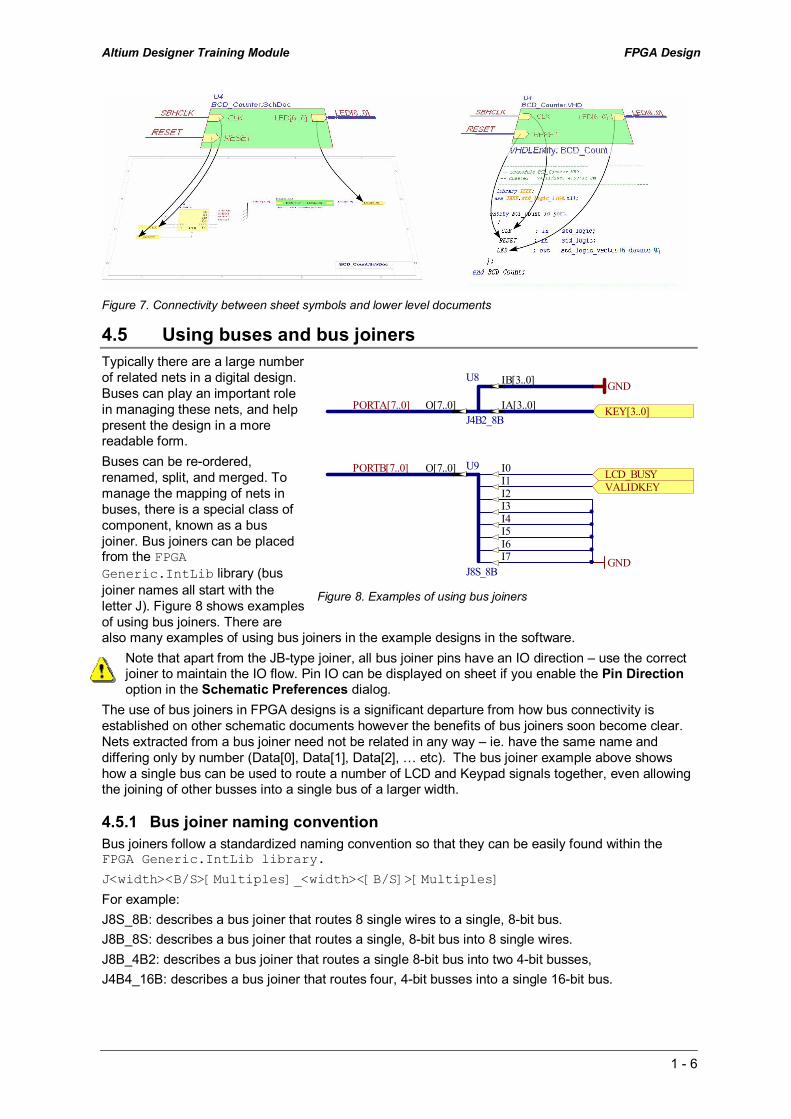
Figure 6. Linking schematic sheet symbols to lower level documents
VHDL or Verilog subdocuments are referenced in the same way as schematic subsheets, by specifying the subdocument filename in the sheet symbol that represents it. The connectivity is from the sheet symbol to an entity declaration in the VHDL file or the Verilog module. To reference an entity with a name that is different from the source HDL filename, include the VHDLEntity or VerilogModule parameter in the sheet symbol whose value is the name of the Entity / Module declared in the source file (as shown above).
4.4 Establishing connectivity between documents Hierarchical net and bus connectivity between documents obeys the standard hierarchical project connection behavior, where ports on the subdocument connect to sheet entries of the same name in the sheet symbol that represents that document, as shown below.
Altium Designer Training Module FPGA Design
1 6
Figure 7. Connectivity between sheet symbols and lower level documents
4.5 Using buses and bus joiners Typically there are a large number of related nets in a digital design. Buses can play an important role in managing these nets, and help present the design in a more readable form. Buses can be reordered, renamed, split, and merged. To manage the mapping of nets in buses, there is a special class of component, known as a bus joiner. Bus joiners can be placed from the FPGA Generic.IntLib library (bus joiner names all start with the letter J). Figure 8 shows examples of using bus joiners. There are also many examples of using bus joiners in the example designs in the software.
Note that apart from the JBtype joiner, all bus joiner pins have an IO direction – use the correct joiner to maintain the IO flow. Pin IO can be displayed on sheet if you enable the Pin Direction option in the Schematic Preferences dialog.
The use of bus joiners in FPGA designs is a significant departure from how bus connectivity is established on other schematic documents however the benefits of bus joiners soon become clear. Nets extracted from a bus joiner need not be related in any way – ie. have the same name and differing only by number (Data[0], Data[1], Data[2], … etc). The bus joiner example above shows how a single bus can be used to route a number of LCD and Keypad signals together, even allowing the joining of other busses into a single bus of a larger width.
4.5.1 Bus joiner naming convention Bus joiners follow a standardized naming convention so that they can be easily found within the FPGA Generic.IntLib library. J<width><B/S>[Multiples]_<width><[B/S]>[Multiples] For example: J8S_8B: describes a bus joiner that routes 8 single wires to a single, 8bit bus. J8B_8S: describes a bus joiner that routes a single, 8bit bus into 8 single wires. J8B_4B2: describes a bus joiner that routes a single 8bit bus into two 4bit busses, J4B4_16B: describes a bus joiner that routes four, 4bit busses into a single 16bit bus.
KEY[3..0]
VALIDKEY LCD_BUSY
GND
O[7..0] IA[3..0]
IB[3..0] U8
J4B2_8B
GND
I1 I0
I2 I3 I4 I5 I6 I7
O[7..0] U9
J8S_8B
PORTB[7..0]
PORTA[7..0]
Figure 8. Examples of using bus joiners

Altium Designer Training Module FPGA Design
1 7
4.5.2 Bus joiner splitting / merging behaviour The basic rule is that bus joiners separate/merge the bits (or bus slice) from least significant bit (or slice) down to most significant bit (or slice). For example, in Figure 9, U17 splits the incoming 8bit bus on pin I[7..0] into two 4bit bus slices, OA[3..0] and OB[3..0]. Obeying the least to most mapping at the slice level, the lower four bits of the input bus map to OA[3..0], and the upper four bits map to OB[3..0]. Following this through to the bit level, I0 will connect to OA0, and I7 will connect to OB3. The joiner U27 merges the four incoming 4bit slices into a 16bit bus. With this joiner IA0 connects to O0, and ID3 connects to O15.
4.5.3 Matching buses of different widths using the JBtype bus joiner
The JBtype bus joiner allows you to match nets in buses of different widths. It does this via 2 component parameters, IndexA and IndexB that map from one bus through to the other bus. These indices must be defined when you use a JB joiner.
Figure 10. Join buses of different widths, and control the nettonet mapping
Read the flow of nets through a JBtype bus joiner by matching from the nets in the attached bus, to the first index on the bus joiner, to the second index in the bus joiner, to the nets defined in the second bus net label. Left Bus ↔ IndexA ↔ IndexB ↔ Right Bus The rules for matching nets at each of the ↔ points are as follows:
Figure 11. An example of using the JB bus joiner to achieve subset mapping
• If both bus ranges are descending, match by same bus index (one range must lie within the other for valid connections). In Figure 11 the matching is:
ADDR9 ↔ IndexA9 ↔ IndexB9 ↔ ROMADDR9, thru to ADDR0 ↔ IndexA0 ↔ IndexB0 ↔ ROMADDR0
(In this example ROMADDR10 thru ROMADDR13 will be unconnected)
Figure 12. Using of a bus joiner for offset mapping
• In Figure 12 the matching is:
INPUTS15 ↔ IndexA15 ↔ IndexB31 ↔ PORTB31, thru to INPUTS0 ↔ IndexA0 ↔ IndexB0 ↔ PORTB16
Figure 9. Bus joiners merge and split buses

Altium Designer Training Module FPGA Design
1 8
Figure 13. Using a bus joiner for range inversion
• If one bus range is descending and another is ascending, the indices are matched from left to right. In Figure 13 the matching is:
INPUTS0 ↔ IndexA15 ↔ IndexB31 ↔ PORTB31, thru to INPUTS15 ↔ IndexA0 ↔ IndexB16 ↔ PORTB16
Figure 14. Another example of using a bus joiner for range inversion
• In Figure 14 the matching is:
INPUTS15 ↔ IndexA15 ↔ IndexB31 ↔ PORTB0, thru to INPUTS0 ↔ IndexA0 ↔ IndexB16 ↔ PORTB15
Altium Designer Training Module FPGA Design
1 9
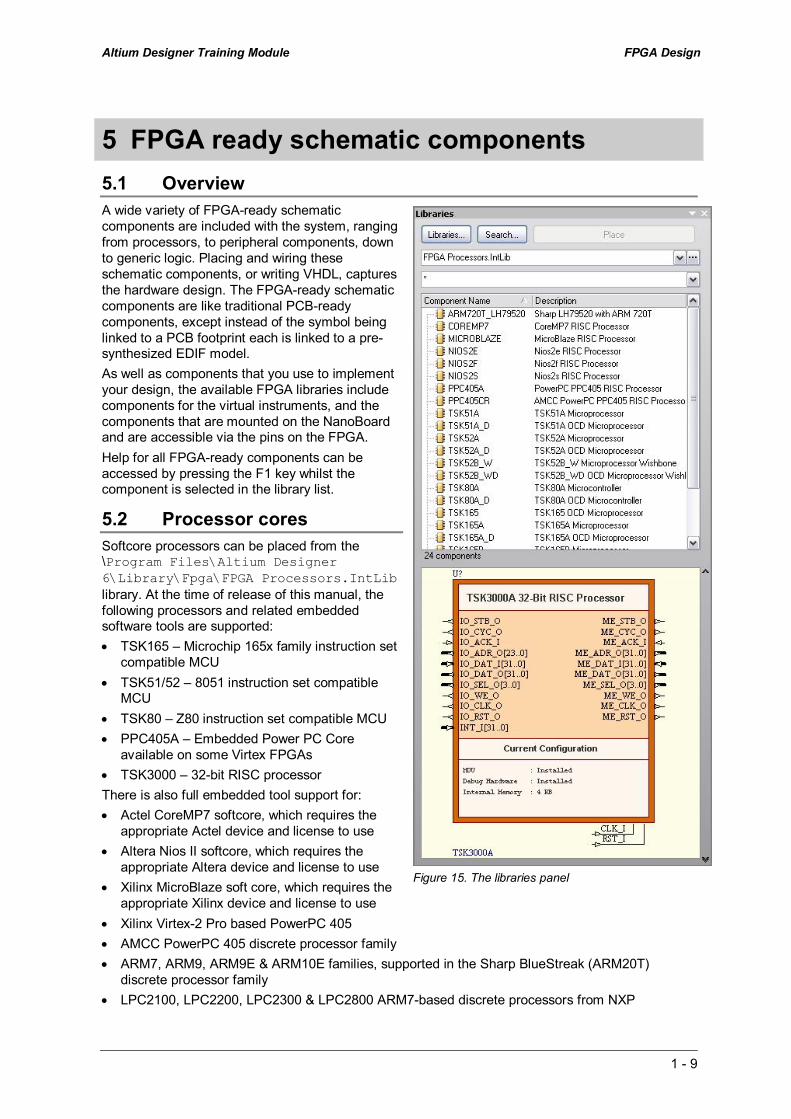
5 FPGA ready schematic components 5.1 Overview A wide variety of FPGAready schematic components are included with the system, ranging from processors, to peripheral components, down to generic logic. Placing and wiring these schematic components, or writing VHDL, captures the hardware design. The FPGAready schematic components are like traditional PCBready components, except instead of the symbol being linked to a PCB footprint each is linked to a pre synthesized EDIF model. As well as components that you use to implement your design, the available FPGA libraries include components for the virtual instruments, and the components that are mounted on the NanoBoard and are accessible via the pins on the FPGA. Help for all FPGAready components can be accessed by pressing the F1 key whilst the component is selected in the library list.
5.2 Processor cores Softcore processors can be placed from the \Program Files\Altium Designer 6\Library\Fpga\FPGA Processors.IntLib library. At the time of release of this manual, the following processors and related embedded software tools are supported: • TSK165 – Microchip 165x family instruction set
compatible MCU • TSK51/52 – 8051 instruction set compatible
MCU • TSK80 – Z80 instruction set compatible MCU • PPC405A – Embedded Power PC Core
available on some Virtex FPGAs • TSK3000 – 32bit RISC processor There is also full embedded tool support for: • Actel CoreMP7 softcore, which requires the
appropriate Actel device and license to use • Altera Nios II softcore, which requires the
appropriate Altera device and license to use • Xilinx MicroBlaze soft core, which requires the
appropriate Xilinx device and license to use • Xilinx Virtex2 Pro based PowerPC 405 • AMCC PowerPC 405 discrete processor family • ARM7, ARM9, ARM9E & ARM10E families, supported in the Sharp BlueStreak (ARM20T)
discrete processor family • LPC2100, LPC2200, LPC2300 & LPC2800 ARM7based discrete processors from NXP
Figure 15. The libraries panel

Altium Designer Training Module FPGA Design
1 10
5.3 Desktop NanoBoard port plugins Hardware resources on the Desktop NanoBoard can be accessed via the use of components from the \Program Files\Altium Designer 6\Library\Fpga\FPGA NB2DSK01 Port Plugin.IntLib library.
5.4 Peripheral Components Many of the hardware resources present on the NanoBoard come with peripheral modules that can be included in the FPGA design to ease interfacing to the external port. Peripherals can be placed from the \Program Files\Altium Designer 6\Library\Fpga\FPGA Peripherals.IntLib library.
5.5 Generic components Generic components can be placed from the library \Program Files\Altium Designer 6\Library\Fpga\FPGA Generic.IntLib. This library is included to implement the interface logic in your design. It includes pinwide and buswide versions for many components, simplifying the wiring complexity when working with buses. As well as a broad range of logic functions, the generic library also includes pullup and pulldown components as well as a range of bus joiners, used to manage the merging, splitting and renaming of buses. For a definition of the naming convention used in the generic library and a complete listing of available devices, refer to the document: CR0118 FPGA Generic Library Guide.pdf. Wild card characters can be used to filter when searching the component library.
5.6 Vendor macro and primitive libraries
If vendor independence is not required, there are also complete primitive and macro libraries for the currently supported vendors/device families. These libraries can be found in the respective Actel, Altera, Lattice and Xilinx subfolders in \Program Files\Altium Designer 6\Library\. The macro and primitive library names end with the string *FPGA.IntLib. Note that some vendors require you to use primitive and macro libraries that match the target device. Designs that include vendor components cannot be retargeted to another vendor’s device.
Figure 16. Using wildcards to quickly find a specific component in the Generic Library

Altium Designer Training Module FPGA Design
1 11
5.7 Exercise 1 – Create a PWM In this exercise we will create our first FPGA design. In order to complete this task you will need to use the following components from their respective libraries:
1. Open a new FPGA Project. Save it as MyPWM.PrjFpg 2. Add a new schematic to your project and save it as MyPWM.SchDoc 3. Place and wire the components to create the Pulse Width Modulator 4. Using components from the two libraries FPGA Generic.IntLib and FPGA NanoBoard
Port Plugin.IntLib, place and wire the schematic shown in Figure 17.
Component Library Name in Library
CLK_BRD FPGA NB2DSK01 PortPlugin.IntLib CLOCK_BOARD
TEST_BUTTON FPGA NB2DSK01 PortPlugin.IntLib TEST_BUTTON
SW[7..0] 1 2 3 4 5 6 7 8
ON FPGA NB2DSK01 PortPlugin.IntLib DIPSWITCH
LEDS[7..0] FPGA NB2DSK01 PortPlugin.IntLib LED
CLR
CEO TC
CEC
Q[7..0]
U1 CB8CEB FPGA Generic.IntLib CB8CEB
U2
INV
FPGA Generic.IntLib INV
A[7..0] B[7..0]
GT LT
U3
COMPM8B
FPGA Generic.IntLib COMPM8B
I1 I0
I2 I3 I4 I5 I6 I7
O[7..0] U4
J8S_8B
FPGA Generic.IntLib J8S_8B

Altium Designer Training Module FPGA Design
1 12
Figure 17. Save your work – we will continue with this schematic soon
CLK_BRD
TEST_BUTTON
SW[7..0] 1 2 3 4 5 6 7 8
ON
LEDS[7..0]
CLR
CEO TC
CEC
Q[7..0]
U1 CB8CEB
U2
INV
A[7..0] B[7..0]
GT LT
U3
COMPM8B
I1 I0
I2 I3 I4 I5 I6 I7
O[7..0] U4
J8S_8B
VCC
GND

Altium Designer Training Module FPGA Design
1 13
6 Targeting the design The schematic that we have just created contains all of the connectivity that must occur internally on our FPGA device but we still need some further information to map the ports on the FPGA schematic to physical pins on an actual FPGA device. This process is called targeting our design.
6.1 Constraint files Rather than storing device and implementation specific data such as pin allocations and electrical properties in the source HDL or schematic documents, this information is stored in separate files – called Constraint files. This decoupling of the logical definition of an FPGA design from its physical implementation allows for quick and easy retargeting of a single design to multiple devices and PCB layouts. Below we see a conceptual representation of an FPGA design sitting inside an FPGA device. The red lines indicate the porttopin mappings that would be handled by the constraint file.
Figure 18. Conceptual view showing the linkage of ports on an FPGA schematic routed to physical device pins.

Altium Designer Training Module FPGA Design
1 14
6.2 Configurations A Configuration is a set of one or more constraint files that must be used to target a design for a specific output. The migration of a design from prototype to production will often involve several PCB iterations and possibly even different FPGA devices. In this case, a separate configuration would be used to bring together constraint file information from each design iteration. Each new configuration (and its associated constraint file(s) is stored with the project and can be recalled at any time. Because configurations can contain multiple constraint files, it can sometimes be helpful to split constraint information across multiple constraint files. Usually one would separate the constraint files according to the class of information they contain:
6.2.1 Device and board constraint information: The specific FPGA device must be identified and ports defined in the top level FPGA design must be mapped to specific pin numbers.
6.2.2 Device resource constraint information: In some designs it may be advantageous to make use of vendor specific resources that are unique to a given FPGA device. Some examples are hardware multiplication units, clock multipliers and memory resources.
6.2.3 Project or design constraint information: This would include requirements which are associated with the logic of the design, as well as constrains on its timing. For example, specifying that a particular logical port must be allocated to global clock net, and must be able to run at a certain speed.
6.3 NanoBoard constraint files Constraint files for use with the NanoBoard daughter / peripheral board modules can be found in the \Program Files\Altium Designer 6\Library\Fpga directory. To protect these system files from inadvertent modification, it is advisable to make this directory ‘read only’.
6.4 Configuration Manager The grouping of multiple constraints into a single configuration is managed via the Configuration Manager; accessible by rightclicking the FPGA project in the Projects panel and selecting Configuration Manager from the menu.
Figure 19. Configuration Manager showing multiple configurations and constraint files.
Figure 19 shows the Configuration Manager dialog for a project that contains multiple configurations and constraint files. The Constraint files are listed in the left column and can be included in a Configuration (listed as the headings in the four right columns) by placing a tick at the row/column intersection point. Although this example only shows one constraint file being used in each of the configurations, there is no reason why a constraint file can’t be used by more than one configuration nor is there any reason why a configuration can’t make use of multiple constraint files.

Altium Designer Training Module FPGA Design
1 15
6.5 Auto Configuring an FPGA project Configuring a design for use with the Desktop NanoBoard has been almost completely automated with the introduction of the Auto Configuration option in Altium Designer. From the Devices View located under View»Devices View or alternatively accessed from the
icon in the toolbar, simply rightclick the image of the Desktop NanoBoard and select the option Configure FPGA Project»<Project Name>.
Figure 20. Auto configuring an FPGA
This will automatically configure the FPGA Project to include the constraint files required to target the hardware on the Desktop Nanoboard and will launch the Configuration Manager dialog for the current FPGA project.
Figure 21. Auto configuration displayed in the configuration manager
6.6 Defining constraints manually Often it is necessary to manually create design constraints. These include constraints for such physical attributes as the frequency of a system clock, or the association of signals to specific device pins (such as one might expect to find when targeting a design for a user board). To create a user constraint file, right click the FPGA project and select Add New to Project»Constraint File. This will create a new blank constraint file and add it to the project.
Figure 22. New blank constraint file
Altium Designer Training Module FPGA Design
1 16
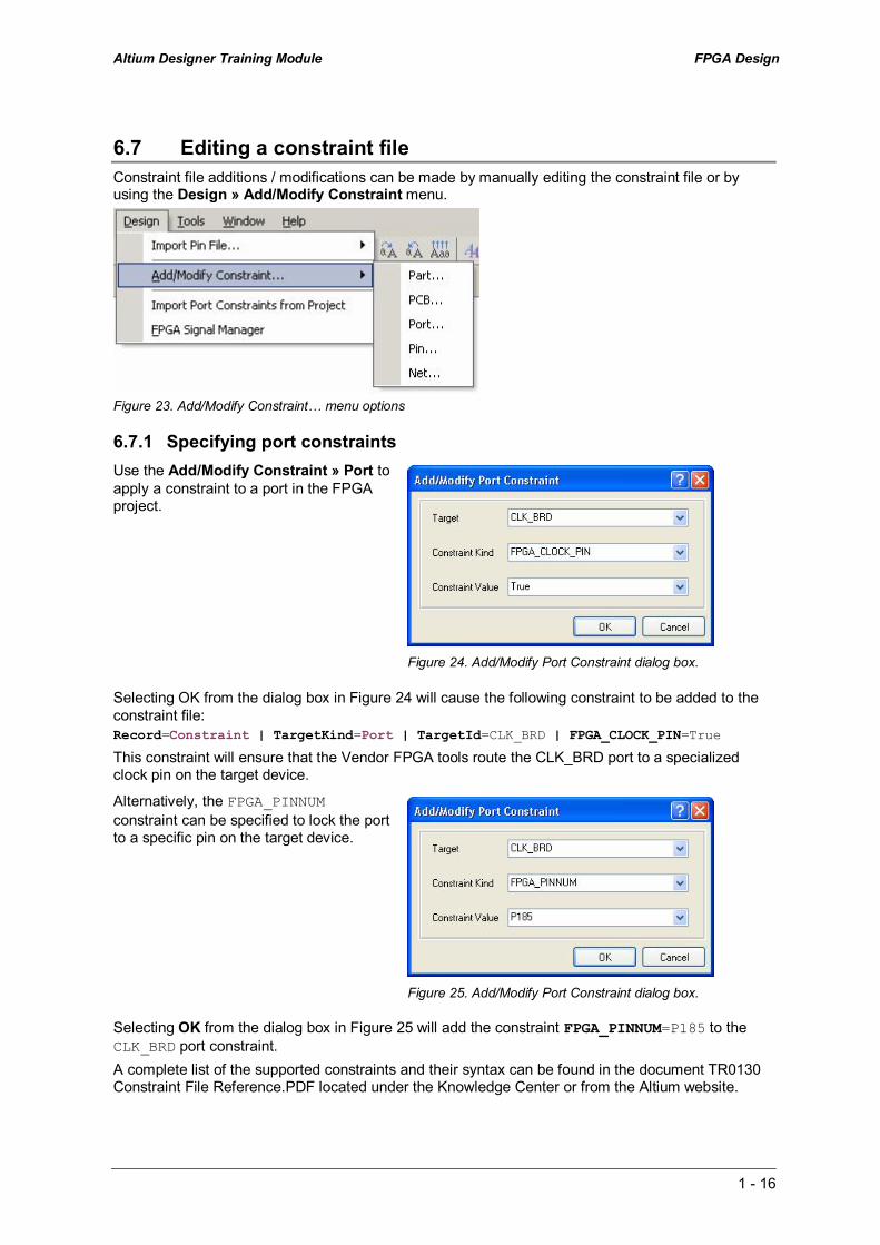
6.7 Editing a constraint file Constraint file additions / modifications can be made by manually editing the constraint file or by using the Design » Add/Modify Constraintmenu.
Figure 23. Add/Modify Constraint… menu options
6.7.1 Specifying port constraints Use the Add/Modify Constraint » Port to apply a constraint to a port in the FPGA project.
Figure 24. Add/Modify Port Constraint dialog box.
Selecting OK from the dialog box in Figure 24 will cause the following constraint to be added to the constraint file: Record=Constraint | TargetKind=Port | TargetId=CLK_BRD | FPGA_CLOCK_PIN=True
This constraint will ensure that the Vendor FPGA tools route the CLK_BRD port to a specialized clock pin on the target device.
Alternatively, the FPGA_PINNUM constraint can be specified to lock the port to a specific pin on the target device.
Figure 25. Add/Modify Port Constraint dialog box.
Selecting OK from the dialog box in Figure 25 will add the constraint FPGA_PINNUM=P185 to the CLK_BRD port constraint. A complete list of the supported constraints and their syntax can be found in the document TR0130 Constraint File Reference.PDF located under the Knowledge Center or from the Altium website.
Altium Designer Training Module FPGA Design
1 17
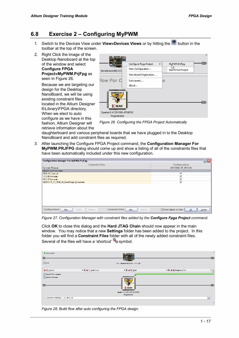
6.8 Exercise 2 – Configuring MyPWM 1. Switch to the Devices View under View»Devices Views or by hitting the button in the
toolbar at the top of the screen. 2. Right Click the image of the
Desktop Nanoboard at the top of the window and select Configure FPGA Project»MyPWM.PrjFpg as seen in Figure 26. Because we are targeting our design for the Desktop NanoBoard, we will be using existing constraint files located in the Altium Designer 6\Library\FPGA directory. When we elect to auto configure as we have in this fashion, Altium Designer will retrieve information about the daughterboard and various peripheral boards that we have plugged in to the Desktop NanoBoard and add constraint files as required.
3. After launching the Configure FPGA Project command, the Configuration Manager For MyPWM.PRJFPG dialog should come up and show a listing of all of the constraints files that have been automatically included under this new configuration.
Figure 27. Configuration Manager with constraint files added by the Configure Fpga Project command.
Click OK to close this dialog and the Hard JTAG Chain should now appear in the main window. You may notice that a new Settings folder has been added to the project. In this folder you will find a Constraint Files folder with all of the newly added constraint files. Several of the files will have a ‘shortcut’ symbol.
Figure 28. Build flow after auto configuring the FPGA design.
Figure 26. Configuring the FPGA Project Automatically

Altium Designer Training Module FPGA Design
1 18
4. The autoconfiguration process deals with the mapping of ports defined on the toplevel FPGA schematic document and their target FPGA pins. There are, however, additional constraints (such as the clock frequency) that are important for the design but which can not be handled automatically. In order to capture this information, it is best to create another constraint file that is reserved for this information and add it to the configuration. Right click the FPGA project and select Add New to Project»Constraint File to add a new, blank constraint file.
5. Save the new constraint file with the name MyConstraint.constraint 6. Select Design>>Add/Modify Constraint… >> Port … . 7. In the Add/Modify Port Constraint dialog set the Target to CLK_BRD 8. Set the Constraint Kind to FPGA_CLOCK_FREQUENCY 9. Set the Constraint Value to 50MHz. 10. Click OK to close the Add/Modify Port Constraint dialog. 11. Observe that a new constraint record has been added to MyConstraints.Constraint.
12. Save your work. 13. Return to the Configuration Manager and add MyConstraint.Constraint to the existing
configuration. 14. Save your project.

Altium Designer Training Module FPGA Design
1 19
7 Running the design Having just configured our design for the NanoBoard the next step is to build and run the design on the NanoBoard.
7.1 Overview Before an FPGA design can be downloaded onto its target hardware, it must first undergo a multi stage build process. This process is akin to the compilation process that software undergoes in order to create a selfcontained program. In this section we will discuss the various steps necessary to build an FPGA design to the point where it is ready to be downloaded onto the target device.
7.2 Controlling the build process The process of converting a schematic or VHDL description of a digital circuit into a bit file that can be downloaded onto an FPGA is quite complex. Fortunately, Altium Designer goes to great lengths to ensure that navigation through this process is as easy as possible. As a vendor independent FPGA development tool, Altium Designer provides a transparent interface to the vendor specific back end tools. Currently Altium Designer supports interaction with Actel Designer (Actel), Quartus II (Altera), ispLEVER (Lattice), and ISE (Xilinx) to perform FPGA processing. This is all handled seamlessly through the Devices View (View » Devices). The Devices View provides the central location to control the process of taking the design from the capture state through to implementing it in an FPGA.
Figure 29. Devices view of an FPGA design that is yet to be processed.
When run in the Live mode, Altium Designer is intelligent enough to detect which daughter board device is present on the Desktop NanoBoard. In the above instance, it has detected that the Spartan3 daughter board is installed. With this information, it then searches the current project’s configuration list to see if any configurations match this device. If more than one configuration is found, the drop down list below the device icon will be populated with a list of valid configurations. If no configuration can be found, the list will display the following:
Figure 30. This message indicates that the project is not configured to target the available FPGA.
Assuming a valid configuration can be found, the simplest way to build and download a design onto the NanoBoard is to leftclick on the Program FPGA button. This will invoke the appropriate build processes that need to be run. In the above example where no previous builds have taken place, all processes will need to be run. In other situations where a project has just been modified, it may be necessary for only a subset of the build processes to run.

Altium Designer Training Module FPGA Design
1 20
7.3 Understanding the build process
Figure 31. Navigating through the Build Process flow.
Building an FPGA project requires processing through a number of stages. Navigation through the build process is accomplished via the four steps circled in Figure 31. The function of each stage will be explained shortly.
7.4 Button regions Each of the main buttons displayed in the build flow have several regions that provide information or control over the individual build stage.
7.4.1 Status LED
The colored indicator tells you the status of that particular step in the overall build flow.
Grey Not Available The step or stage cannot be run.
Red Missing The step or stage has not been previously run.
Yellow Out of Date A source file has changed and the step or stage must be run again in order to obtain up to date file(s).
Blue Running The step or stage is currently being executed.
Orange Cancelled – The step or stage has been halted by user intervention.
Magenta Failed An error has occurred while running the current step of the stage.
Green Up to Date – The step or stage has been run and the generated file(s) are up to date.
7.4.2 Run all
Clicking on the ‘arrow’ icon will force the current stage and all prior stages to run regardless of whether they have run to completion previously. Selecting this icon will force a totally clean build even if the design has been partially built.
7.4.3 Run
Selecting the ‘label’ region will run the current stage and any previous dependant stages that are not up to date. This is the quickest way to build a design as it only builds those portions of the design that actually require it.

Altium Designer Training Module FPGA Design
1 21
7.4.4 Show substages
Selecting the ‘down arrow’ will expose a drop down list of the various substages for the current build stage. The status of the various substages is indicated by the color of the status ‘LED’. Where a substage has failed, the associated report file can be examined to help determine the cause of the failure.
Figure 32. Substages available under the main build stage.
7.5 Accessing stage reports / outputs All generated output files are stored in a folder with the same name as the configuration used for the associated project. This folder is located at the output path defined in the Options tab of the Options for Project dialog (Project » Project Options). In general only files that are created as part of the build process should be located here. This ensures that projects can be compacted by deleting this directory without fear of loss of important information.
Where a report is available upon running a stage step, clicking on the associated icon can access it. Use this feature to access detailed information relating to why a specific stage may have failed to build.
7.6 Build stages We will now explain the different stages in the build process.
7.6.1 Compile
Figure 33. Compile stage of the process flow.
This stage of the process flow is used to perform a compile of the source documents in the associated FPGA project. If the design includes any microprocessor cores, the associated embedded projects are also compiled – producing a Hex file in each case. This stage can be run with the Devices view configured in either Live or Not Live mode. The compile process is identical to that performed from the associated Project menu. Running this stage can verify that the captured source is free of electrical, drafting and coding errors. Note: The source FPGA (and embedded) project(s) must be compiled – either from the Projects panel or by running the Compile stage in the Devices view – in order to see Nexusenabled device entries in the Soft Devices region of the Devices view.

Altium Designer Training Module FPGA Design
1 22
7.6.2 Synthesize
Figure 34. Synthesize stage of the process flow.
This stage of the process flow is used to synthesize the compiled FPGA project, as well as any other components that need to be generated and synthesized to specific device architectures. The vendor place and route tools subsequently use the synthesis files generated, during the build stage of the flow. Running this stage will determine whether the design is synthesizable or not. This stage can be run with the Devices view configured in either Live or Not Live mode. The actual steps involved in providing a toplevel EDIF netlist and satellite synthesis model files for use by the next stage in the process flow can be summarized as follows: • The cores for any design/device specific blocks used in the FPGA design will be autogenerated
and synthesized (e.g. a block of RAM wired to an OCDversion micro controller for use as external Program memory space). These synthesized models will contain compiled information from the embedded project (Hex file).
• The main FPGA design is then synthesized. An intermediate VHDL or Verilog file will be generated for each schematic sheet in the design and a toplevel EDIF netlist will be created using these and any additional HDL source files.
• For the particular physical device chosen, synthesized model files associated with components in the design will be searched for and copied to the relevant output folder. Both System and User presynthesized models are supported.
• The toplevel folder for System presynthesized models is the \Program Files\Altium Designer 6\Library\Edif folder, which is subdivided by Vendor and then further by device family.
• The toplevel folder for user presynthesized models is defined in the Synthesis page of the FPGA Preferences dialog, accessed under the Toolsmenu.
• The following list summarizes the order (top to bottom = first to last) in which folders are searched when looking for a synthesized model associated with a component in the design: FPGA project folder User models top folder\Vendor folder\Family folder User models top folder\Vendor folder User models top folder System models top folder (Edif)\Vendor Folder\Family folder System models top folder (Edif)\Vendor folder System models top folder (Edif).
7.6.3 Build
Figure 35. Build stage of the process flow for Xilinx devices.
This stage of the process flow is used to run the vendor place and route tools. This stage can be run with the Devices view configured in either live or not live mode.

Altium Designer Training Module FPGA Design
1 23
Running the tools at this stage can verify if a design will indeed fit inside the chosen physical device. You may also wish to run the Vendor tools if you want to obtain pin assignments for importing back into the relevant constraint file. The end result of running this stage is the generation of an FPGA programming file that will ultimately be used to program the physical device with the design. There are essentially five main stages to the build process: • Translate Design – uses the toplevel EDIF netlist and synthesized model files, obtained from
the synthesis stage of the process flow, to create a file in Native Generic Database (NGD) format – i.e. vendor tool project file
• Map Design to FPGA – maps the design to FPGA primitives • Place and Route takes the lowlevel description of the design (from the mapping stage) and
works out how to place the required logic inside the FPGA. Once arranged, the required interconnections are routed
• Timing Analysis – performs a timing analysis of the design, in accordance with any timing constraints that have been defined. If there are no specified constraints, default enumeration will be used
• Make Bit File – generates the programming file that is required for downloading the design to the physical device.
When targeting a Xilinx device, an additional stage is available – Make PROM File. This stage is used when you want to generate a configuration file for subsequent download to a Xilinx configuration device on a Production board. After the Build stage has completed, the Results Summary dialog will appear (Figure 36). This dialog provides summary information with respect to resource usage within the target device. Information can be copied and printed from the dialog. The dialog can be disabled from opening, should you wish, as the information is readily available in the Output panel or from the report files produced during the build.
Figure 36. Summarizing resource usage for the chosen device.

Altium Designer Training Module FPGA Design
1 24
7.6.4 Program
Figure 37. Program FPGA stage of the process flow.
This stage of the process flow is used to download the design into the physical FPGA device on a NanoBoard or production board. This stage is only available when the Devices view is configured in Live mode. This stage of the flow can only be used once the previous three stages have been run successfully and a programming file has been generated. A green arrow will point to the device to be programmed in the Hard Devices Chain.
Figure 38. Successful programming of the physical FPGA device.
As the programming file is downloaded to the device via the JTAG link, the progress will be shown in the Status bar. Once successfully downloaded, the text underneath the device will change from ‘Reset’ to ‘Programmed’ (Figure 38) and any Nexusenabled devices on the soft chain will be displayed as ‘Running’ (Figure 39).
Figure 39. Soft devices running after successful program download.
7.7 Configuring a build stage Should you wish to configure any of the specific options associated with each of the different substages in the FPGA build flow, you can do so by clicking on the appropriate configuration icon. Consider the case where you want to generate a PROM file for subsequent download to a Xilinx configuration device on a production board. In the process flow associated to the targeted FPGA device, expand the build section. The last entry in the build menu is Make PROM File
Clicking on the icon, to the far right of this menu entry, will open the Options for PROM File Generation dialog (Figure 41). From here you can choose the nonvolatile configuration device that will be used by the production board to store the FPGA configuration.
Figure 41. Accessing the options dialog for PROM file generation.

Altium Designer Training Module FPGA Design
1 25
7.8 How Altium Designer interacts with backend vendor tools If you are already familiar with the build flows offered by Altera and Xilinx, you will be familiar with one or both of the following panels:
Figure 42. Xilinx (left) and Altera (right) vendor tool interfaces.
Although Altium Designer has its own HDL synthesizer, it is reliant on backend vendor tools to implement the design on a specific device. This makes sense, as it is the device vendors who have the most intimate knowledge of their specific devices and who have already developed wellproven targeting technologies. Most vendor specific tools have been developed in a modular fashion and contain a number of separate executable programs for each phase of the implementation process. The vendor GUIs that are presented to the user are cocoordinating programs that simply pass the appropriate parameters to backend, commandline programs. When it comes to FPGA targeting, Altium Designer operates in a similar fashion in that it acts as a coordinator of backend, vendorspecific programs. Parameters that need to be passed from the Altium Designer frontend to the vendorspecific backend programs are handled by a series of text based script files. Users who are already familiar with the backend processing tools may find some use in accessing these script files should they wish to modify or ‘tweak’ interaction with backend processing tools. This however is considered a highly advanced topic and one that should be handled cautiously. Ensure backups are taken prior to modification. The files controlling interaction with vendorspecific backend tools can be found in the System directory under the Altium Designer 6 install directory. The naming convention used for these files is: Device[Options | Script]_<vendor>[_<tool> | <family>].txt …so for example DeviceOptions_Xilinx_PAR.txt controls the default options for Xilinx’s Place and Route tool.
7.9 Exercise 3 – Run MyPWM on the NanoBoard In this exercise we shall take our previously developed PWM design and run it on the NanoBoard. 1. Ensure that the NanoBoard is correctly connected to the PC, the XC3S15004FG676C daughter
board is loaded, and the NanoBoard is switched on. 2. Open the Devices View and ensure the Live checkbox is ticked. 3. Click on the ‘label’ region of the Program FPGA button in the FPGA Build flow. The design will
begin building and may take a moment or two to complete. 4. If any build errors occur, diagnose and rectify the error and attempt the build process again. 5. Once downloaded, verify the operation of the design by switching different DIP switches off and
on. You should notice a change in the LED illumination.
Altium Designer Training Module FPGA Design
1 26
8 Embedded instruments 8.1 Overview So far we have built our PWM FPGA design and run it on the NanoBoard. Fortunately this design provided an output on the LEDs that enabled us to immediately verify that the circuit was performing as we expected. But how do we verify other designs? In this section we will introduce the range of embedded instruments that can be integrated into FPGA designs to facilitate onchip testing and debugging.
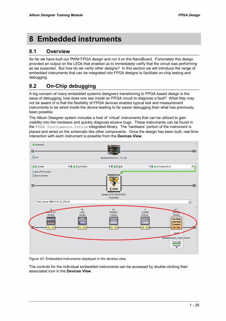
8.2 OnChip debugging A big concern of many embedded systems designers transitioning to FPGA based design is the issue of debugging; how does one see inside an FPGA circuit to diagnose a fault? What they may not be aware of is that the flexibility of FPGA devices enables typical test and measurement instruments to be wired inside the device leading to far easier debugging than what has previously been possible. The Altium Designer system includes a host of ‘virtual’ instruments that can be utilized to gain visibility into the hardware and quickly diagnose elusive bugs. These instruments can be found in the FPGA Instruments.IntLib integrated library. The ‘hardware’ portion of the instrument is placed and wired on the schematic like other components. Once the design has been built, real time interaction with each instrument is possible from the Devices View.
Figure 43. Embedded instruments displayed in the devices view.
The controls for the individual embedded instruments can be accessed by doubleclicking their associated icon in the Devices View.

Altium Designer Training Module FPGA Design
1 27
8.3 CLKGEN
Figure 44. Frequency generator, used to generate the specified frequency
The frequency generator outputs a 50% duty cycle square wave, of the specified frequency. Clicking the appropriate button can choose a number of predefined frequencies, or a custom frequency can be selected using the Other Frequency button. If the specified frequency cannot be generated the closest possible is generated and the error shown on the display. Note that when the frequency generator is instantiated in the FPGA it will not be running, you must click the Run button to generate an output.
8.4 CROSSPOINT_SWITCH
Figure 45.Cross point switch, used to control the connection between input and output signals
The CROSSPOINT_SWITCH device is a configurable signal switching instrument which provides an efficient means by which to switch signals in a design. The interconnection between input and output blocks is completely configurable. Initial connections can be defined as part of designtime configuration, but can be changed onthe fly at runtime, from the device's associated instrument panel. The latter enables you to switch signals without having to re synthesize and download the entire design to the FPGA.
8.5 FRQCNT2
Figure 46. Frequency counter, used to measure frequency in the design
The frequency counter is a dual input counter that can display the measured signal in 3 different modes; as a frequency, period, or number of pulses.
Frequency Generator
TIMEBASE FREQ
U7
CLKGEN
Frequency Counter
FREQA FREQB
TIMEBASE
U6
FRQCNT2
Crosspoint Switch AIN_A[7..0] AIN_B[7..0]
BIN_A[7..0] BIN_B[7..0]
AOUT_A[7..0] AOUT_B[7..0]
BOUT_A[7..0] BOUT_B[7..0]
U18
CROSSPOINT_SWITCH

Altium Designer Training Module FPGA Design
1 28
8.6 IOB_x
Figure 47. Digital IO module, used to monitor and control nodes in the design
The digital I/O is a generalpurpose tool that can be used for both monitoring and activating nodes in the circuit. It is available in either 8bit wide or 16bit wide variants, with 1 to 4 channels. Each input bit presents as a LED, and the set of 8 or 16 bits also presents as a HEX value. Outputs can be set or cleared individually by clicking the appropriate bit in the Outputs display. Alternatively typing in a new HEX value in the HEX field can alter the entire byte or word. If a HEX value is entered you must click the
button to output it. The Synchronize button can be used to transfer the current input value to the outputs.
8.7 DIGITAL_IO
Figure 48. Configurable Digital IO module, used to monitor and control nodes in the design
The configurable digital I/O is a generalpurpose tool that can be used for both monitoring and activating nodes in the circuit. Unlike its legacy counterparts (IOB_x family of devices), with the DIGITAL_IO device you are not constrained to limited signals of 8 or 16bits. Instead, any number of signals may be added, and any number of bits can be assigned to a single signal. You may also have different numbers of input and output signals.
Each input bit can be presented in a range of different styles including LEDs, numeric, LED digits, or as a bar, and the set of bits also presents as a HEX value. Output styles can also vary and include LEDs, numeric, LED digits, and a slider. Each output can have a predefined Initial Value and will also include a HEX display. Outputs can be set or cleared individually and the method will vary with the style selected. Alternatively typing in a new HEX value in the HEX field can alter the value of the output. If a HEX value is entered you must click the button to output it. The Synchronize button can be used to transfer the current input value to the outputs.
Configurable Digital IO InLEDs[7..0] SpareOutB[7..0] SpareOutC[7..0] SpareOutD[7..0]
Rot[7..0] Zoom[7..0] Flags[7..0]

Altium Designer Training Module FPGA Design
1 29
8.8 LAX_x
Figure 49. The logic analyzer instrument at the top, with two variations of the configurable LAX shown below it. The LAX component on the left has been configured to accept 3 different sets of 64 signals (signal sets), the one on the right has one signal set of 16 bits. The Configure dialog is used to set the capture width, memory size and the signal sets.
The logic analyzer allows you to capture multiple snapshots of multiple nodes in your design. Use the LAX to monitor multiple nets in the design and display the results as a digital or an analog waveform. The LAX is a configurable component. Configure it to simultaneously capture 8, 16, 31 or 64 bits. The number of capture snapshots is defined by the amount of capture memory; this ranges from 1K to 4K of internal storage memory (using internal FPGA memory resources). It can also be configured to use external memory. This requires you to wire it to FPGA memory resources or to offchip memory (e.g. Desktop NanoBoard Memory). After placing the configurable LAX from the library, rightclick on the symbol and select Configure from the floating menu to open the Configure (logic analyzer) dialog, where you can define the Capture width, memory size and the signal sets. The Configurable LAX includes an internal multiplexer, this allows you to switch from one signal set to another at run time, displaying the capture data of interest. You can also trigger off one signal set while observing the results of another set.
Note that the FPGA Instruments library includes a number of LAX components. The LAX component is the configurable version, all others are legacy versions.

Altium Designer Training Module FPGA Design
1 30
8.8.1 Waveform display features
Figure 50. Digital waveform capture results from the logic analyzer
Figure 51. Analog waveform capture results from the logic analyzer
The capture results are displayed in the instrument panel. There are also two waveform display modes. The first is a digital mode, where each capture bit is displayed as a separate waveform and the capture events define the timeline. Note that the capture clock must be set in the logic analyzer options for the timeline to be calculated correctly. Click the Show Digital Waves button to display the digital waveform. The second waveform mode is an analog mode, where the value on all the logic analyzer inputs is displayed as a voltage, for each capture event. The voltage range is from zero to the maximum possible count value, scaled to a default of 3.3V. Click the Show Analog Waves button to display the analog waveform.
8.8.2 Zooming in and out In both the analog and digital waveform viewers it is possible to zoom in and out by hitting the Page Up or Page Down keys respectively
8.8.3 Continuous display mode Waveforms captured by the logic analyzer can be displayed as a single pass or as a continuously updated display. Continuous updates can be enabled / disabled from the logic analyzer toolbar.
Figure 52. Enabling the continuous capture mode.

Altium Designer Training Module FPGA Design
1 31
8.9 Terminal Console
Figure 53. Terminal console instrument rack functions as a debug console for embedded applications.
The TERMINAL device is a debug console which allows you to type text directly in its associated instrument panel and send it directly to the processor in your design, to be handled by the embedded software code running therein. Conversely, it allows the display of text sent from that processor. Although classed as one of Altium Designer's virtual instruments, the TERMINAL device is really a hybrid – part instrument and part Wishbonecompliant slave peripheral. Whereas other instruments are configured and operated directly from a GUI, the TERMINAL device requires interaction at the code level, to initialize internal registers and to write to/read from its internal storage buffers.
8.10 Exercise 4A – Using embedded instruments A working design of a PWM circuit complete with embedded instruments has been prepared to illustrate the features of FPGA instruments. Your instructor will tell you where to find it on your local hard drive.
TEST_BUTTON
LEDS[7..0]
CLR
CEO TC
CEC
Q[7..0]
U1 CB8CEB
U2
INV
A[7..0] B[7..0]
GT LT
U3
COMPM8B
I1 I0
I2 I3 I4 I5 I6 I7
O[7..0] U4
J8S_8B
VCC
GND
CLK_BRD CLK_BRD
CLK_BRD
Frequency Generator
TIMEBASE FREQ
U7
CLKGEN CLK_TICK
Logic Analyser
CLK CLK_CAP CHANNELS[15..0]
TRIGGER
STATUS
U5
LAX_1K16
CLK_BRD CLK_TICK
O[15..0] IA[7..0]
IB[7..0] U6
J8B2_16B
Frequency Counter
FREQA FREQB
TIMEBASE
U9
FRQCNT2
CLK_BRD
CLK_TICK
TCK TMS
TDI TDO
TRST
JTAG
.
JTAG
JTAG
JTAG
JTAG
JTAG
. . VCC
JTAG_NEXUS_TMS JTAG_NEXUS_TCK JTAG_NEXUS_TDO JTAG_NEXUS_TDI
1 Ch x 8 Bit Digital IO
AIN[7..0] AOUT[7..0]
U8
IOB_1X8
Figure 54. PWM circuit with several embedded instruments connected.
1. Open the provided project and download it to your NanoBoard. 2. Follow on your own circuit as the instructor discusses the various embedded instruments.
CLK_I RST_I
DAT_I[7..0] DAT_O[7..0] ADR_I[3..0]
CYC_I STB_I
WE_I
ACK_O
INT_O[1..0]
Terminal Console U1
TERMINAL

Altium Designer Training Module FPGA Design
1 32
3. Doubleclick the NanoBoard icon in the Devices View to open the instrument rack for the NanoBoard and set its clock frequency to 50MHz.
Figure 55. NanoBoard controller.
4. Open the frequency generator’s instrument panel. If the time base indicated in the window next to the Set Time Base button is not 50 MHz then press the Set Time Base button to open a dialog box that will enable you to set it correctly. The Require 50/50 Duty checkbox should be checked. The frequency generator should be set to 1MHz as indicated in Figure .
Figure 56. Counter options dialog
Figure 57. Frequency generator Panel
5. Open the frequency counter’s instrument panel. Select the Counter Options button on the frequency counter module and make sure the Counter Time Base is also set to 50MHz (the same as the NanoBoard clock frequency), as shown in Figure 57. Press OK. Use the Mode button as necessary on each channel of the frequency counter module to toggle the display mode between frequency, period or count. You should get a similar display to what is depicted in Figure 59.
Figure 58. Counter options dialog

Altium Designer Training Module FPGA Design
1 33
Figure 59. Frequency counter control panel
6. Open the Digital IOB’s instrument panel.
Figure 60. Digital IOB instrument control panel
7. Modify the Outputs of the IOB module and observe changes in the LEDs. 8. Adjust the output frequency of the frequency generator module to a lower frequency; try 1KHz.
Observe the impact this has on the LEDs. Modify the Outputs of the IOB and observe further changes in the LEDs.
9. Adjust the output frequency of the frequency generator module back to 1MHz. 10. Open the logic analyser’s instrument control panel.
Figure 61. Logic analyser instrument control panel
11. Select Show Panel on the logic analyzer. Set the panel up as depicted in Figure 62.
Figure 62. Logic analyser triggering options.

Altium Designer Training Module FPGA Design
1 34
12. Select Options on the logic analyser. Set the clock capture frequency to 1MHz – the same as the frequency generator module. Adjust the other controls to be the same as shown in Figure 63.
13. Select Arm and observe the waveform displayed in the waveform viewer. Select Continuous Capture from the Logic Analyzer menu and adjust the IOB output. Observe the change in the PWM marktospace ratio.
Figure 63. Logic analyser setup options.
Figure 64. Logic analyzer waveform with bit7 of the IOB set.
Figure 65. Logic analyzer waveform with bits 6 & 7 of the IOB set.

Altium Designer Training Module FPGA Design
1 35
8.11 Where are the Instruments? The important differentiator between Altium Designer’s embedded instruments and other simulation based virtual instruments is that Altium Designer’s embedded instruments are true physical devices that are downloaded into the FPGA device as part of the design. The information provided to the designer by the embedded instruments can be relied upon as it is taken from real physical measurements taken on chip. Figure illustrates this point as it shows the FPGA real estate used by the embedded instruments.
Figure 66. Floorplan of MyPWM.SchDoc after it has been placed onto an FPGA.
8.12 Enabling embedded instruments The NanoBoard hardware incorporates the entire infrastructure necessary to support Embedded Instruments and allow them to communicate with the host PC. All virtual instruments communicate with the host PC via a ‘soft’ JTAG chain that conforms to the Nexus standard. To enable Nexus on the NanoBoard, the NEXUS_JTAG_PORT and NEXUS_JTAG_CONNECTOR must be placed onto the top level schematic. These respective components can be found in the FPGA Generic.IntLib and FPGA NB2DSK01 PortPlugin.IntLib Integrated Libraries.

Altium Designer Training Module FPGA Design
1 36
TCK TMS
TDI TDO
TRST
JTAG
.
JTAG
JTAG
JTAG
JTAG
JTAG . .
NEXUS_JTAG_PORT
VCC
JTAG_NEXUS_TMS JTAG_NEXUS_TCK JTAG_NEXUS_TDO JTAG_NEXUS_TDI
NEXUS_JTAG_CONNECTOR
Figure 67. NEXUS JTAG Port and NEXUS JTAG Connector.
To be able to use embedded instruments in custom designs, it is necessary to reserve 4 device pins for the NEXUS_JTAG_CONNECTOR and ensure that sufficient device resources are present to accommodate the virtual instruments in the device. The JTAG soft chain and other communications chains present on the NanoBoard will be discussed further in the next section.

Altium Designer Training Module FPGA Design
1 37
9 Interacting with the NanoBoard 9.1 Overview The NanoBoard is pivotal to rapid embedded systems development with Altium Designer. It contains a range of peripherals and expansion capabilities to allow it to adapt to a broad cross section of embedded projects. In this section we will discuss the concepts necessary for a designer to make effective use the NanoBoard’s potential.
9.2 NanoBoard communications The NanoBoard contains 3 primary communication channels. A complete understanding of these channels is not necessary to begin using the tool suite however it may be of interest to developers keen to make use of Altium Designer’s debugging capabilities on their own custom designs. The primary point of user control of the NanoBoard is via the Devices View. This view provides an easytouse visualization of the various communications chains active on the NanoBoard.
Figure 68. Devices view with its various communications channels highlighted.
NanoTalk Chain
JTAG Hard Chain
JTAG Soft Chain

Altium Designer Training Module FPGA Design
1 38
9.2.1 NanoTalk chain NanoTalk is the proprietary communications protocol developed by Altium to enable multiple NanoBoards to communicate with one another. The 10 pin NanoTalk headers can be found on both the left and right edges at the upper end of the Desktop NanoBoard. Communications via this channel is totally transparent to the user. There should be no need to interact with this standard.
9.2.2 JTAG Hard Chain The JTAG Hard Chain is a serial communications channel that connects physical devices together. JTAG devices can be connected end on end by connecting the TDO pin of an upstream device to the TDI pin of a downstream device. The hard JTAG chain is visible in the middle portion of the Devices View. Usually this is where an FPGA will be located however if you also have other devices that are connected to the JTAG chain such as a configuration device then these will be visible also. The hard JTAG chain can be extended beyond the NanoBoard through the User Board A and User Board B connectors. When using either of these connectors, it is imperative that the JTAG chain is not broken – i.e. the TDI/TDO chain must be looped back to the NanoBoard.
9.2.3 JTAG Soft Chain The JTAG Soft Chain is a separate JTAG channel that provides communication with the Embedded Instruments that can be incorporated into an FPGA design. This chain is labeled as a soft chain since it does not connect tangible physical devices together but rather connects soft or downloadable instruments that reside inside a hard or physical FPGA device.
9.3 Technical background
Figure 69. Conceptual View of JTAG data flows.
9.3.1 JTAG in depth The acronym JTAG stands for Joint Test Application Group and is synonymous with IEEE 1149.1. The standard defines a Test Access Port (TAP), boundary scan architecture and communications protocol that allows automated test equipment to interact with hardware devices. Essentially it enables you to place a device into a test mode and then control the state of each of the device’s pins or run a builtin selftest on that device. The flexibility of the JTAG standard has also lead to its usage in programming (configuring) devices such as FPGAs and microprocessors. At minimum, JTAG requires that the following pins are defined on a JTAG device: TCK: Test Clock Input TMS: Test Mode Select
J JT TA AG G C Ce el ll l P Pa ar ra al ll le el l
D Da at ta a F Fl lo ow w
T TD DI I
T TD DO O

Altium Designer Training Module FPGA Design
1 39
• TDI: Test Data Input • TDO: Test Data Output
TCK controls the data rate of data being clocked into and out of the device. A rising TCK edge is used by the device to sample incoming data on its TDI pin and by the host to sample outgoing data on the devices TDO pin.
Figure 70. Using JTAG Chain to connect multiple JTAG devices together in a digital design.
Figure 70. JTAG Test Access Port (TAP) State Machine.
The Test Access Port (TAP) Controller is a state machine that controls access to two internal registers – the Instruction Register (IR) and the Data Register (DR). Data fed into the device via TDI or out of the device via TDO can only ever access one of these two registers at any given time. The register being accessed is determined by which state the TAP controller is in. Traversal through the TAP controller state machine is governed by TMS.

Altium Designer Training Module FPGA Design
1 40
9.3.2 Nexus 5001 The flexibility of JTAG for hardware debugging purposes has flowed over into the software domain. In the same way that test engineers have sought a standardized method for testing silicon, software engineers have also sought a standardized means for debugging their programs. In 1998, the Global Embedded Debug Interface Standard (GEDIS) Consortium was formed. In late 1999 the group moved operations into the IEEEISTO and changed their name to the Nexus 5001 Forum and released V1.0 of IEEEISTO – 1999. In December 2003, V2.0 was released. The Nexus 5001 standard provides a standardized mechanism for debug tools to interact with target systems and perform typical debugging operations such as setting breakpoints and analyzing variables, etc. There are 4 classes of Nexus compliance – each with differing levels of supported functionality. The lowest level uses JTAG as the lowlevel communications conduit. The implementation of Nexus 5001 on the Desktop NanoBoard has been labeled as the JTAG Soft Chain. It is a serial chain just like the hard chain however rather than connecting physical devices together, it connects virtual devices together. These devices include the set of virtual instruments that are supplied with Altium Designer and described in the following chapter. Control of devices on the Soft Chain can be performed from the Devices View – Soft Chain Devices are located towards the bottom of the Devices View under the Hard Chain. As with the JTAG Hard Chain, the Soft Chain can be taken off the NanoBoard via the User Board A and User Board B connectors. This provides the means for target systems to also include virtual instruments and to benefit from the Altium Designer development environment. Similarly to the Hard Chain, it is imperative that a complete loop be maintained between the Soft Chain TDI and TDO connections.
9.4 The NanoBoard controller The NanoBoard Controller can be accessed by doubleclicking on the NanoBoard icon in the Devices View.
Figure 71. The NanoBoard Controller Instrument Rack.
The Clock Frequency indicated in the window will be supplied to the CLK_BRD port on the NanoBoard. Accessing this clock on custom designs is
as simple as placing the CLOCK_BOARD component from the FPGA NB2DSK01 Port Plugin.IntLib Library. Selecting a nonstandard frequency is possible by clicking the Other Frequency button. The NanoBoard clock system employs a serially programmable clock source (part number ICS30702) that is capable of synthesizing any clock frequency between 6 and 200MHz. Advanced access to the Clock Control IC registers is available through the Clock Control Options button. A datasheet for this device is available from the ICS website http://www.icst.com/products/pdf/ics3070102.pdf. An online form useful for calculating settings for the clock control IC is also available at http://www.icst.com/products/ics307inputForm.html.
To the right of the NanoBoard Controller is a section with the heading Flash RAM. The FPGA Boot button affords the facility to store a daughter board configuration file that will get automatically loaded into the daughter board on power up. The Embedded button exposes memory that can be used by the user application to store nonvolatle user data. The Embedded Memory device is accessible via the SERIALFMEMORY component in the FPGA NB2DSK01 PortPlugin.IntLib Library.
CLK_BRD P182 P182

Altium Designer Training Module FPGA Design
1 41
9.5 FPGA I/O view To display the Instrument rack for a device, doubleclick on the device in the JTAG Hard chain. Clicking on the JTAG Viewer Panel button then brings up the JTAG Viewer Panel.
Figure 72. The Hard Devices instrument rack.
Figure 73. The FPGA I/O Instrument Rack and JTAG Viewer Panel.
This interface enables the developer to see in real time the flow of signals across the device’s pins. This can be particularly useful when ensuring that signals are being correctly propagated to and from the device.
Placing a tick in the Live Update checkbox will cause the display to update in real time. Alternatively, leaving the Live Update checkbox clear and selecting the update icon will cause
signal information to be latched to the display and held. Check Hide Unassigned I/O Pins to remove clutter from the display. The BSDL Information drop down list should only need to be accessed for devices which are unknown to Altium Designer. In this case, you will need to provide the location of the vendor supplied BSDL file for the device you are viewing. The FPGA IO instrument rack is available for all devices on the JTAG Hard Chain – including devices on a user board that is connected to the JTAG Hard Chain.

Altium Designer Training Module FPGA Design
1 42
9.6 Live cross probing Probe directives can be placed on the FPGA schematic on any I/O net and will update in real time as long as the Hard Devices Instrument Panel is displayed. Use the Place » Directives » Probe to place a cross probe on one of the I/O nets.
Figure 74. Using Live Cross Probing.
9.7 Exercise 4B – View MyPWM on the NanoBoard 1. Reload your circuit from Exercise 3 again and run it on the NanoBoard. 2. Open the JTAG Viewer Panel. 3. Check the Hide Unassigned I/O Pins checkbox and the Live Update checkboxes. 4. Observe the change in switch states and LEDs as you toggle the NanoBoard DIP switches. 5. Use the Place » Directives » Probe option to place a probe point on the bus connected to the
DIP Switches. Observe the probe value as the DIP Switches are changed on the NanoBoard.

Altium Designer Training Module FPGA Design
1 43
10 Creating a core component 10.1 Core project Altium Designer provides the ability to encapsulate an entire FPGA circuit into a single component that can be used as a building block in other projects. These selfcontained blocks are called core components and offer the advantage of design reuse and design security. Core components can be synthesized for a target FPGA and made available to others without exposing the underlying IP. A core project is used to create an FPGA component that may be used multiple times within one or across many FPGA projects. The output of a core project behaves in a similar fashion to a library component in that it becomes an elemental unit that is used as a component in larger designs. A core project is useful when you wish to make some functionality available to a broad user base but you do not want to expose the IP used to implement the functionality.
Figure 75. Using a core component in an FPGA Project.
10.2 Creating a core component from an FPGA project It is possible to create a core component from scratch however often we wish to create a core component from an existing FPGA design or project. In either case a blank core project must first be created. If the core component is to be based on an existing design then use Project » Add Existing to Project to add the relevant VHDL, Verilog and / or schematic documents to the project. If the core component is being created from scratch then its source documents will need to be created in the same way that an FPGA project is built.
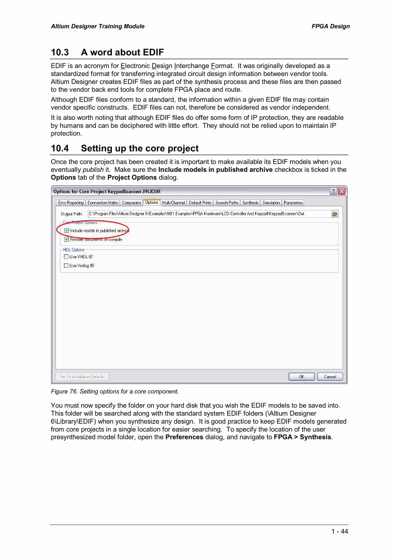
Altium Designer Training Module FPGA Design
1 44
10.3 A word about EDIF EDIF is an acronym for Electronic Design Interchange Format. It was originally developed as a standardized format for transferring integrated circuit design information between vendor tools. Altium Designer creates EDIF files as part of the synthesis process and these files are then passed to the vendor back end tools for complete FPGA place and route. Although EDIF files conform to a standard, the information within a given EDIF file may contain vendor specific constructs. EDIF files can not, therefore be considered as vendor independent. It is also worth noting that although EDIF files do offer some form of IP protection, they are readable by humans and can be deciphered with little effort. They should not be relied upon to maintain IP protection.
10.4 Setting up the core project Once the core project has been created it is important to make available its EDIF models when you eventually publish it. Make sure the Include models in published archive checkbox is ticked in the Options tab of the Project Options dialog.
Figure 76. Setting options for a core component.
You must now specify the folder on your hard disk that you wish the EDIF models to be saved into. This folder will be searched along with the standard system EDIF folders (\Altium Designer 6\Library\EDIF) when you synthesize any design. It is good practice to keep EDIF models generated from core projects in a single location for easier searching. To specify the location of the user presynthesized model folder, open the Preferences dialog, and navigate to FPGA > Synthesis.

Altium Designer Training Module FPGA Design
1 45
Figure 77. Specifying the location of core component models.
10.5 Constrain / configure The concept of constraint files and configurations is central to the flexibility of Altium Designer. They provide a mechanism to allow FPGA circuits to be developed independent of the final physical implementation. Rather than storing device and implementation specific data such as pin allocations and electrical properties in the source VHDL or schematic documents, this information is stored in separate files – called Constraint files. This decoupling of the logical definition of an FPGA design from its physical implementation allows for quick and easy retargeting of a single design to multiple devices and PCB layouts. There are a number of classes of configuration information pertinent to different aspects of an FPGA project:
10.5.1 Device and board considerations: The specific FPGA device must be identified and ports defined in the top level FPGA design must be mapped to specific pin numbers.
10.5.2 Device resource considerations: In some designs it may be advantageous to make use of vendor specific resources that are unique to a given FPGA device. Some examples are hardware multiplication units, clock multipliers and memory resources.

Altium Designer Training Module FPGA Design
1 46
10.5.3 Project or design considerations: This would include requirements which are associated with the logic of the design, as well as constraints on its timing. For example, specifying that a particular logical port must be allocated to global clock net, and must be able to run at a certain speed. A configuration is a set of one or more constraint files that must be used to target a design for a specific output. The migration of a design from prototype, refinement and production will often involve several PCB iterations and possibly even different devices. In this case, a separate configuration would be used to bring together constraint file information for each design iteration. Each new configuration (and its associated constraint file(s) is stored with the project and can be recalled at any time. To summarize: • Constraint files store implementation specific information such as device pin allocations and
electrical properties. • A Configuration is a grouping of one or more constraint files and describes how the FPGA
project should be built.
10.6 Creating a new constraint file When targeting a design for a user board, it is often necessary to manually create at least one constraint file. This constraint file would include at a minimum the device that is being targeted and may include any number of additional constraints appropriate for the target PCB. As cores may often be synthesized for a number of possible targets, it is useful to discuss the process of manually constraining and configuring a design in the context of creating core projects. Before a configuration can be built, a constraint file must exist. Constraint files have the extension .Constraint. Constraint files for use with the Desktop NanoBoard can be found in the \Program Files\Altium Designer 6\Library\Fpga\ directory. In general it is advisable to take a copy of these files and store it in your project directory before adding it to the project. This way the project is kept selfcontained and any edits you may inadvertently make will not affect the supplied constraint file. • To add your own, new constraint file, right click on the project name in the Projects panel and
select Add New To Project » Constraint File. • A new blank constraint file will appear. To specify the target device select Design » Add/Modify
Constraint » Part and the Browse Physical Devices dialog will open.
Figure 78. The Browse Physical Devices dialog, where you select the target FPGA.

Altium Designer Training Module FPGA Design
1 47
Figure 79. Basic constraint file.
• Select the vendor, family, device and temperature/speed grades as desired and click OK. A line similar to the one above will be automatically inserted into the constraint file:
• Save the constraint file. Typically it would be named to reflect its role – for example if the target device was a Xilinx Spartan3 FPGA mounted on your project PCB you might call it MyProject_Spartan3_1500.Constraint. You will notice the constraint file has been added to the project under the settings tab.
Figure 80. Project with constraint File.
10.7 Creating a configuration As previously mentioned, configurations group a number of constraint files together to create a set of instructions for the FPGA build process. To define a configuration: • Rightclick on the project name in the Projects panel and select Configuration Manager
Figure 81. Specifying a configuration using the configuration manager.
• If you have just recently created a new constraints file, you will see it listed under the Constraint Filename. Existing constraint files that currently aren’t in the project can be added by selecting the Add button next to the Constraint Files text.
• To define a new configuration, select the Add button next to the Configurations text. A dialog will appear requesting you to provide a name for the new configuration. The name can be arbitrary but it is helpful if it provides some indication as to what the configuration is for.

Altium Designer Training Module FPGA Design
1 48
• Having defined the new configuration, you may now assign constraint files to it by ticking their associated checkbox. Here we have assigned the constraint file MyConstraint_Spartan3_1500 to the Target_XC3S1500 configuration.
• Click OK to save the configuration.
Figure 82. Specifying a configuration using the configuration manager.
Although the above simplistic example only had one constraint file and one configuration, the power of configurations really becomes apparent as the design matures. Below we see how a design has been targeted to multiple platforms:
Figure 83. Example of a project with multiple configurations defined.
Configurations can be updated or modified as desired at any time throughout the project’s development by returning to the Configuration Manager dialog.
10.8 Synthesize Now that we have defined a configuration we are ready to synthesize the core for the target. • With the top level FPGA document open
select Design » Synthesize. If we had defined more than one configuration and wished to synthesize all configurations at once we could select Design » Synthesize All Configurations.
• If you have not already nominated the top level entity/configuration in the Synthesis tab of the Options for Core Project, the Choose Toplevel dialog will appear. Enter the core project name or select from the dropdown list and click OK to continue.
• The project will be synthesized resulting in the generation of VHDL files for the schematic, EDIF files for the schematic wiring and parts, and a synthesis log file. These will all be located under the Generated folder in the project panel.
• You will observe the configuration name in brackets beside the Generated Folder. Had we synthesized more than one configuration then a separate Generated folder would have appeared for each of the defined configurations.
Figure 84. Specifying an FPGA project’s top level document.
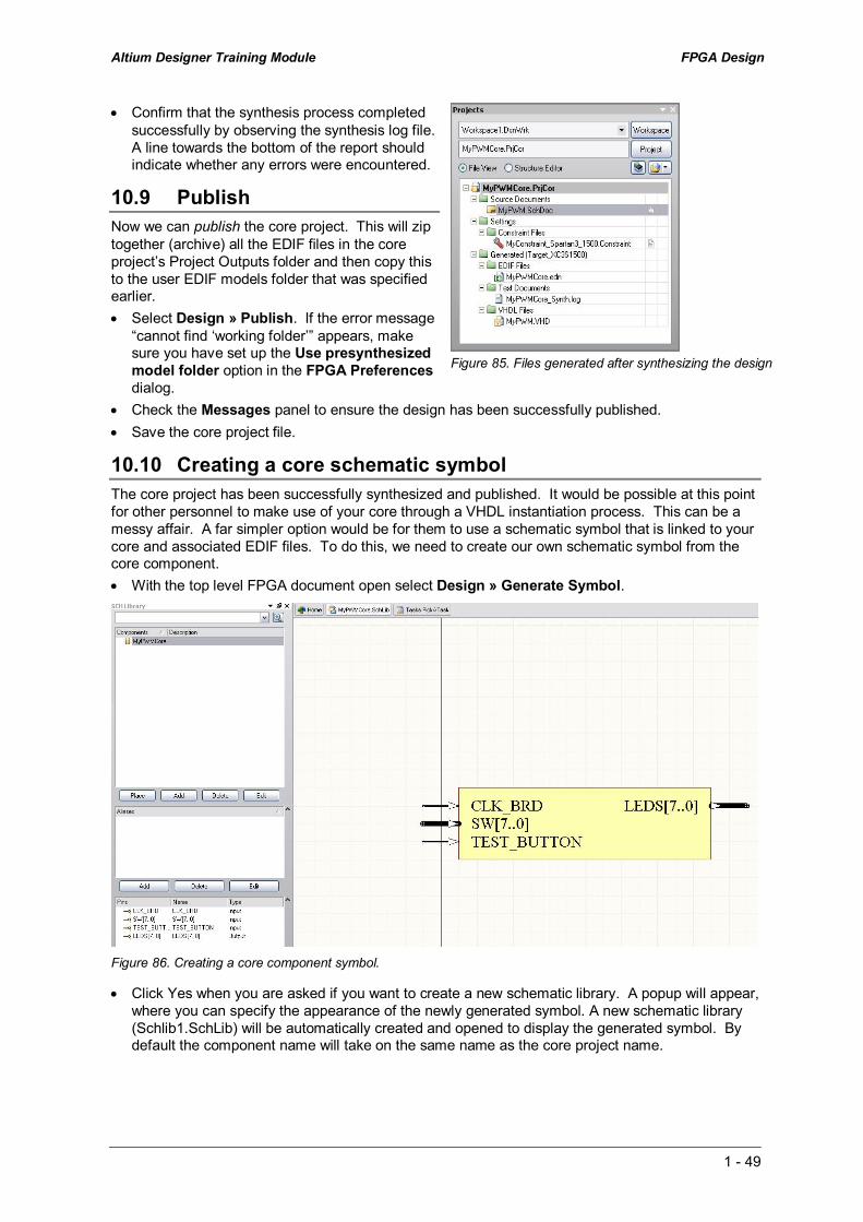
Altium Designer Training Module FPGA Design
1 49
Figure 85. Files generated after synthesizing the design
• Confirm that the synthesis process completed successfully by observing the synthesis log file. A line towards the bottom of the report should indicate whether any errors were encountered.
10.9 Publish Now we can publish the core project. This will zip together (archive) all the EDIF files in the core project’s Project Outputs folder and then copy this to the user EDIF models folder that was specified earlier. • Select Design » Publish. If the error message
“cannot find ‘working folder’” appears, make sure you have set up the Use presynthesized model folder option in the FPGA Preferences dialog.
• Check the Messages panel to ensure the design has been successfully published. • Save the core project file.
10.10 Creating a core schematic symbol The core project has been successfully synthesized and published. It would be possible at this point for other personnel to make use of your core through a VHDL instantiation process. This can be a messy affair. A far simpler option would be for them to use a schematic symbol that is linked to your core and associated EDIF files. To do this, we need to create our own schematic symbol from the core component. • With the top level FPGA document open select Design » Generate Symbol.
Figure 86. Creating a core component symbol.
• Click Yes when you are asked if you want to create a new schematic library. A popup will appear, where you can specify the appearance of the newly generated symbol. A new schematic library (Schlib1.SchLib) will be automatically created and opened to display the generated symbol. By default the component name will take on the same name as the core project name.

Altium Designer Training Module FPGA Design
1 50
Figure 87. Specifying core component options.
• From within the library editor, select the component in the Library panel and select the Edit button. The Library Component Properties dialog will be displayed. Note that several parameters have been added to indicate which child models are required to be retrieved from the published EDIF zip files.
Figure 88. Specifying the properties of the newly created core component symbol.
• Clicking on the Edit Pins button will enable further modification of the properties and appearance of the schematic symbol.
• From the schematic library editor, adjust the symbol properties as appropriate and save the component. Save the library before exiting.
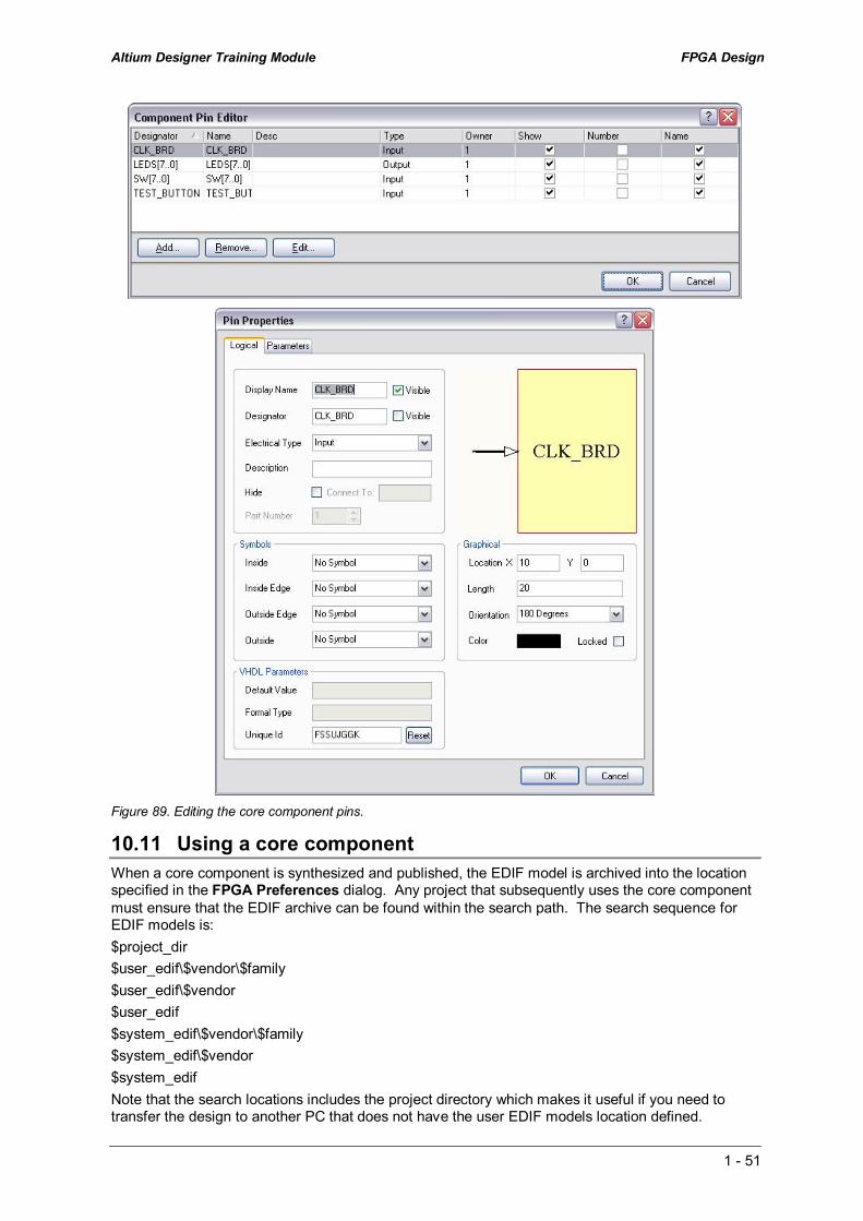
Altium Designer Training Module FPGA Design
1 51
Figure 89. Editing the core component pins.
10.11 Using a core component When a core component is synthesized and published, the EDIF model is archived into the location specified in the FPGA Preferences dialog. Any project that subsequently uses the core component must ensure that the EDIF archive can be found within the search path. The search sequence for EDIF models is: $project_dir $user_edif\$vendor\$family $user_edif\$vendor $user_edif $system_edif\$vendor\$family $system_edif\$vendor $system_edif Note that the search locations includes the project directory which makes it useful if you need to transfer the design to another PC that does not have the user EDIF models location defined.

Altium Designer Training Module FPGA Design
1 52
10.12 Exercise 5 – Create a core component from MyPWM 1. Create a new core project and call it MyPWMCore.PrjCor. Note that the filename must not have
spaces in it. 2. Set the “Include models in published archive” checkbox in the Project Options dialog. 3. In the Preferences dialog, go to FPGA – Synthesis, and select an output path for EDIF files.
This path should not include any spaces. 4. Attach the existing MyPWM.SchDoc that you created as part of exercise 3. 5. Create a project level constraint file and call it MyPWMPrj.Constraint. Add the following to this
constraint file: Record=Constraint | TargetKind=Port | TargetId=CLK_BRD | FPGA_CLOCK_PIN=True Record=Constraint | TargetKind=Port | TargetId=CLK_BRD | FPGA_CLOCK=True Record=Constraint | TargetKind=Port | TargetId=CLK_BRD | FPGA_CLOCK_FREQUENCY=50Mhz Figure 90. Updates to be made to MyPWMPrj.Constraint file.
6. Create a constraint file each for an Altera Cyclone II device as well as a Xilinx Spartan 3 device. 7. Create a configuration that links each of the individual device constraint files with the project
constraint file. 8. Synthesize all configurations and publish the design. Check the User Presynthesized model
Folder (as set in Step 3) using windows explorer and view the directories that are created and their contents.
9. Create a core schematic symbol and save it to the library MyCoreLib.SchLib 10. Create a new FPGA project and schematic that makes use of your PWM core and test it on the
NanoBoard.
CLK_BRD
SW[7..0]
TEST_BUTTON
LEDS[7..0]
U1
MyPWMCore
CLK_BRD
TEST_BUTTON
SW[7..0] 1 2 3 4 5 6 7 8
ON
LEDS[7..0]
Figure 90. Test project used to test the function of MyPWMCore.

Altium Designer Training Module FPGA Design
1 53
11 FPGA design simulation Altium Designer supports behavioral simulation of VHDL designs. This is particularly useful when verifying the functional operation of digital circuits prior to implementing them inside an FPGA.
11.1 Creating a testbench Before simulation can begin, a VHDL Testbench file must be created to drive the simulation session. Conceptually, the Testbench straddles the Design Under Test (DUT) and drives the DUT’s inputs whilst observing its outputs.
Figure 91. Conceptual view of how a VHDL testbench interacts with the Design Under Test (DUT).
Altium Designer provides a convenient method for building a VHDL Testbench based on the inputs and outputs of the nominated DUT. A shell testbench file can be automatically created by the system.
• Open a schematic document and select Tools » Convert » Create VHDL Testbench from the menu.
• Open a VHDL document and select Design » Create VHDL Testbench. A new VHDL document will be created with the extension .VHDTST and will be added to the project. Within the Testbench file will be a comment “—insert stimulus here”. By placing VHDL code at this point you can control the operation of the simulation session. At a minimum, the Testbench must set all of the DUT’s inputs to a known state. If the DUT requires a clock then that too must be provided by the Testbench. Most simulation errors occur as a result of the Testbench failing to properly initialize the inputs of the DUT.
11.2 Assigning the Testbench Document Once you have created the Testbench file but before a simulation can begin, Altium Designer needs to be formally told which VHDL document in the project will be used to drive the simulation. Select Project Options by right clicking on the FPGA project in the Projects panel or use the menu to select Project » Project Options Select the Simulation tab from within the Project Options dialog and select the appropriate Testbench Document from the dropdown list.
Figure 9218. Specifying the testbench document
VHDL Testbench
Design Under Test (DUT) DUT Inputs
DUT Outputs

Altium Designer Training Module FPGA Design
1 54
11.3 Initiating a simulation session A simulation session can be initiated by selecting Simulator » Simulate from the menu or by clicking the simulation button in the VHDL Tools toolbar whilst a VHDL document is active in the main window.
11.4 Project compile order When you first run a simulation from a testbench, Altium Designer may need to establish the compilation order of the VHDL documents. Whilst performing this process, you may see an error appear in the Messages panel with the message: “Unbound instance DUT of component …” Do not be concerned as this is normal when you first run a simulation.
Figure 93. Messages panel.
After a brief moment, a dialog may appear prompting you to specify the top level document for simulation (Figure 94). The compilation order of the project can be changed at a later time if necessary by selecting Project » Project Order or by right clicking on the FPGA project in the Projects panel and selecting Project Order.
Figure 94. Choosing the top level document.

Altium Designer Training Module FPGA Design
1 55
Figure 9519. Specifying signals to display in the simulation.
11.5 Setting up the simulation display
The Simulation Signals dialog (Figure 95) is automatically presented at the beginning of a simulation or it can be accessed via Simulator » Signals.
The Watch Name is the name of the signal declared inside the block of VHDL code. Signals must be Enabled in order to be a part of the simulation. Furthermore, if they need to be displayed as part of the simulation output then Show Wave must also be selected. The Waveform viewer (Figure 95) provides a visualization of the status of each of the displayed signals. • The icon next to the bus name indicates a bus
signal. Clicking on this icon will expand the bus into its individual signals for closer inspection.
• The time cursor (indicated by the purple vertical bar) can be dragged along the time axis via the mouse. The current position of the cursor is provided in the time bar across the top of the display.
• Zooming in or out is achieved by pressing the Page Up or Page Down keys respectively.
• The display format of the individual signals can be altered via the menu item Tools » Format and Radix.
.
Figure 96. The waveform viewer
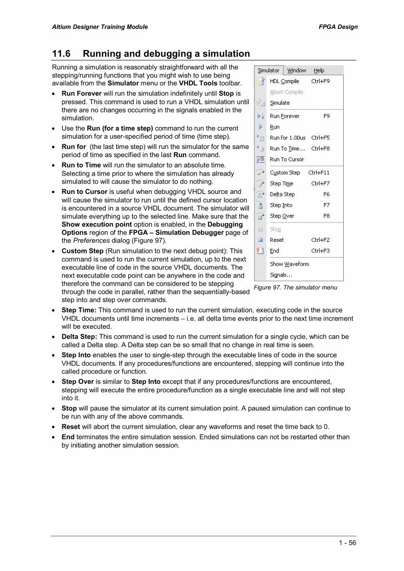
Altium Designer Training Module FPGA Design
1 56
11.6 Running and debugging a simulation Running a simulation is reasonably straightforward with all the stepping/running functions that you might wish to use being available from the Simulator menu or the VHDL Tools toolbar. • Run Forever will run the simulation indefinitely until Stop is
pressed. This command is used to run a VHDL simulation until there are no changes occurring in the signals enabled in the simulation.
• Use the Run (for a time step) command to run the current simulation for a userspecified period of time (time step).
• Run for (the last time step) will run the simulator for the same period of time as specified in the last Run command.
• Run to Time will run the simulator to an absolute time. Selecting a time prior to where the simulation has already simulated to will cause the simulator to do nothing.
• Run to Cursor is useful when debugging VHDL source and will cause the simulator to run until the defined cursor location is encountered in a source VHDL document. The simulator will simulate everything up to the selected line. Make sure that the Show execution point option is enabled, in the Debugging Options region of the FPGA – Simulation Debugger page of the Preferences dialog (Figure 97).
• Custom Step (Run simulation to the next debug point): This command is used to run the current simulation, up to the next executable line of code in the source VHDL documents. The next executable code point can be anywhere in the code and therefore the command can be considered to be stepping through the code in parallel, rather than the sequentiallybased step into and step over commands.
• Step Time: This command is used to run the current simulation, executing code in the source VHDL documents until time increments – i.e. all delta time events prior to the next time increment will be executed.
• Delta Step: This command is used to run the current simulation for a single cycle, which can be called a Delta step. A Delta step can be so small that no change in real time is seen.
• Step Into enables the user to singlestep through the executable lines of code in the source VHDL documents. If any procedures/functions are encountered, stepping will continue into the called procedure or function.
• Step Over is similar to Step Into except that if any procedures/functions are encountered, stepping will execute the entire procedure/function as a single executable line and will not step into it.
• Stop will pause the simulator at its current simulation point. A paused simulation can continue to be run with any of the above commands.
• Reset will abort the current simulation, clear any waveforms and reset the time back to 0. • End terminates the entire simulation session. Ended simulations can not be restarted other than
by initiating another simulation session.
Figure 97. The simulator menu

Altium Designer Training Module FPGA Design
1 57
Figure 98. The simulation debugger options in the preferences dialog.

Altium Designer Training Module FPGA Design
1 58
11.7 Exercise 6 – Create a testbench and simulate MyPWM 1. Open the project you created in Exercise 2 and make MyPWM.VHD the active document. 2. Select Design » Create VHDL Testbench from the menu. Update the testbench to be the
same as the code listed in Figure 99.
Figure 99. Testbench code for testing MyPWM
3. Update the testbench document, toplevel entity/configuration and toplevel architecture fields in the simulation tab of the Project » Project Options dialog.
4. Compile the testbench document and rectify any errors. 5. Run the simulation by selecting Simulator » Simulate. 6. Run the simulator for 2us. 7. Observe the waveforms for LEDS[0] and LEDS[1]. Is it what you expect? Try changing the
PWM period by changing the value of SW in the testbench.

Altium Designer Training Module FPGA Design
1 59
12 Review