FPCCD option of ILD vertex detector Yasuhiro Sugimoto KEK for FPCCD VTX group @LCWS2012.
13
FPCCD option of ILD vertex detector Yasuhiro Sugimoto KEK for FPCCD VTX group @LCWS2012
-
Upload
shannon-obrien -
Category
Documents
-
view
224 -
download
1
Transcript of FPCCD option of ILD vertex detector Yasuhiro Sugimoto KEK for FPCCD VTX group @LCWS2012.
FPCCD option of ILD vertex detector
Yasuhiro Sugimoto
KEK
for FPCCD VTX group
@LCWS2012

Outline
• FPCCD VTX design parameter• FPCCD sensors• Support structure

FPCCD VTX design parameter
• Pixel size of outer layers– It was 5mm, but changed to 10mm
Reduction of number of readout channels and power consumption
Layer R (mm) |Z| (mm) |cosq| Pixel size (mm)
1 16 62.5 0.97 5
2 18 62.5 0.96 5
3 37 125 0.96 10
4 39 125 0.95 10
5 58 125 0.91 10
6 60 125 0.9 10

Power consumption• Assumptions
• Results
Readout frequency 10 Mpix/s
Readout time 200 ms
Clock timing Same for inner and outer layers
Vertical shift time 40 us/line
Power consumption 15 mW/ch
Chip size (in/out) 11x62.5mm2 / 22x125mm2
Number of chips (in/out) 40 (=10x2x2) / 112 (=(11+17)x2x2)
Pixel size (in)
Pixel size (out)
# of ch/chip (in)
# of ch/chip (out)
# of ch (total)
Power consumption
5 um 5 um 28 56 7392 111 W
5 um 10 um 15 15 2280 34 W

Expected IP resolution
• Increase of pixel size of outer layers does not affect the IP resolution
Momentum(GeV/c)1 10 210
(mm
)d0s
-310
-210
stdreco 20 all5um
stdreco 30 all5umstdreco 85 all5um
stdreco 20 5um10umstdreco 30 5um10um
stdreco 85 5um10um

Pixel occupancy
• Simulation results for pixel occupancy at 1TeV (statictics:10BX)
• Increase of occupancy due to decrease of # of pixels (1/4) is less than x4
Layer Occupancy for 5um (%) Occupancy for 10um (%)
Direct B.S. Total Direct B.S. Total
1 5.1 14.5 19.6
2 3.1 7.3 10.4
3 0.18 0.06 0.24 0.41 0.14 0.55
4 0.15 0.06 0.20 0.33 0.13 0.46
5 0.033 0.014 0.047 0.075 0.032 0.107
6 0.029 0.017 0.046 0.064 0.039 0.104

FPCCD sensors
• Small prototype in FY2012– 6mm square image area– 6um pixel size– 4ch/chip with different horizontal shift
register size: 6x6, 6x12, 6x18, 6x24 um2
– It works except for the channel with 6x6um2 horizontal shift register

FPCCD sensors• Large prototype
– 62.4x12.3mm2 image area ~ Real size prototype for inner layers
– 8ch/chip with several pixel sizes: 4chx6um, 2chx8um, 2chx12um
– Si wafer has been made, but waiting for packaging

• Ladder design– Ladder has a tricky shape to
allow overlapping of sensors with adjacent ladder
– Material budget ~0.3%X0/ladder = 0.15%X0/sensor layer
Support structuret (mm)
Total t (mm)
X0 (%)
Si 50 50 0.0534
Epoxi 10 2000 0.0028
FPC Cu 9 0.0125
Kapton 51 0.0179
Epoxi 10 0.0028
CFRP 100 0.0383
Epoxi 20 0.0056
RVC 1600 0.0300
Epoxi 20 0.0056
CFRP 100 0.0383
Epoxi 10 0.0028
FPC Cu 9 0.0125
Kapton 51 0.0179
Epoxi 10 0.0028
Si 50 50 0.0534
Total 2100 0.2966
9

Support structure
• Ladder deformation by self weight– Simplified geometry of 50um Si sensors (200um gap
between two sensors) + CFRP sheets and RVC core
Two edges support:Maximum deformation ~ 8.66 um
One edge fix, one edge support:Maximum deformation ~ 4.76 um

Support structure
• Design in ILD simulation model– Similar to SLD vertex detector– 2 mm thick Be end plate, 0.5 mm thick Be support shell– Kapton+Cu flexible cables– Ladders– 1 cm thick foam of the cryostat
Ti cooling tubeod:2mm, id:1.5mm
FPC; 9mm width x 10/side +17mm width x 28/side
=> 3 layers of 50um Kapton + 9um Cu1573
8
143
62
82
Beryllium shell
Cryostat; 0.2mm CFRP+1cm styrofoam+0.2mm CFRP
Layer 1: 10 ladders
Layer 2: 11 ladders
Layer 3: 17 ladders
FTD-1
Annulus block; 1mm CFRPLadder block; 1.5mm CFRP Beam pipe
164.6175
82
146
0.5 t
0.5t
145

Beryllium support shell
• FEA calculation of deformation– 1kgf (9.8N) is applied in
z-direction– Maximum deformation
is less than 2mm– Total weight is less than
500g max force caused by the friction at the kinematic mount would be less than 500gf (mm)
12
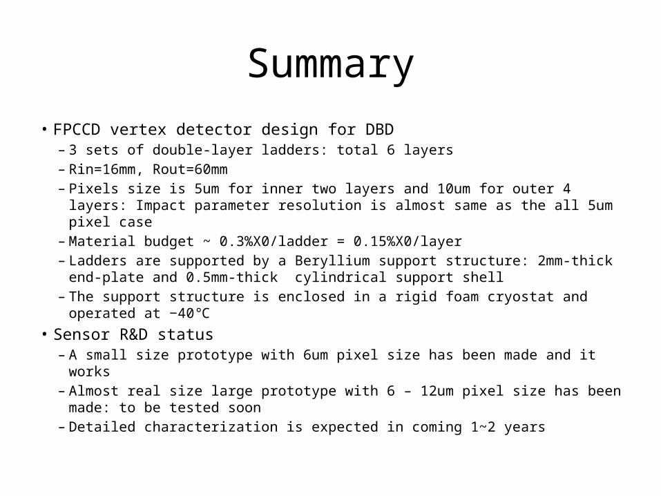
Summary
• FPCCD vertex detector design for DBD– 3 sets of double-layer ladders: total 6 layers– Rin=16mm, Rout=60mm– Pixels size is 5um for inner two layers and 10um for outer 4 layers: Impact
parameter resolution is almost same as the all 5um pixel case– Material budget ~ 0.3%X0/ladder = 0.15%X0/layer– Ladders are supported by a Beryllium support structure: 2mm-thick end-
plate and 0.5mm-thick cylindrical support shell– The support structure is enclosed in a rigid foam cryostat and operated at
−40℃
• Sensor R&D status– A small size prototype with 6um pixel size has been made and it works– Almost real size large prototype with 6 – 12um pixel size has been made:
to be tested soon– Detailed characterization is expected in coming 1~2 years