Force sensors based on piezoresistive and MOSFET ......cortado on the stairs of CNM, conferences,...
203
Force sensors based on piezoresistive and MOSFET cantilevers for biomolecular sensing Thesis presented to apply for the degree of Doctor in Electronic Engineering at the Department of Electronic Engineering of Universitat Autonòma de Barcelona by, Giordano Tosolini Instituto de Microelectrónica de Barcelona Centro Nacional de Microelectrónica IMB-CNM (CSIC) Joan Bausells Roigé (Advisor and University Tutor) Research Professor Instituto de Microelectrónica de Barcelona Centro Nacional de Microelectrónica IMB-CNM (CSIC) and Associate Professor Universitat Autònoma de Barcelona UAB September 2013
Transcript of Force sensors based on piezoresistive and MOSFET ......cortado on the stairs of CNM, conferences,...
Force sensors based on piezoresistive
and MOSFET cantilevers for
biomolecular sensing
Thesis presented to apply for the degree of Doctor in Electronic Engineering at the
Department of Electronic Engineering of Universitat Autonòma de Barcelona
by,
Giordano Tosolini
Instituto de Microelectrónica de Barcelona
Centro Nacional de Microelectrónica
IMB-CNM (CSIC)
Joan Bausells Roigé
(Advisor and University Tutor)
Research Professor
Instituto de Microelectrónica de Barcelona
Centro Nacional de Microelectrónica
IMB-CNM (CSIC)
and
Associate Professor
Universitat Autònoma de Barcelona
UAB
September 2013
©Copyright by Giordano Tosolini
Force sensors based on piezoresistive and MOSFET cantilevers for
biomolecular sensing / by Giordano Tosolini – Consejo Superior de
Investigaciones Científicas (CSIC) and Universitat Autònoma de
Barcelona (UAB), 2010. Thesis
The use of this document is only authorized for private uses, placed
in investigation and teaching activities. Reproduction with lucrative
aims is not authorized. These rights affect all the content of the
thesis. In the using or citation of parts of the thesis, it is obliged to
indicate the name of the author.

I
Joan Bausells, Research Professor at the Instituto de Microelectrónica de Barcelona –
Centro Nacional de Microelectrónica (IMB-CNM, CSIC) and Associate Professor at the
Universitàt Autonoma de Barcelona (UAB)
CERTIFIES:
That the thesis entitled “Force sensors based on piezoresistive and MOSFET cantilevers
for biomolecular sensing” was carried out by Giordano Tosolini under his supervision within
IMB-CNM.
Cerdanyola del Vallès, September 2013.
Prof. Joan Bausells

II

III
Abstract
Biorecognition processes between receptors and their conjugate ligands are very
important in biology. These biomolecules can build up very specific complexes displaying a
variety of functions such as genome replication and transcription, enzymatic activity,
immune response, cellular signaling, etc. The unambiguous one-to-one complementarity
exhibited by these biological partners is widely exploited also in biotechnology to develop
biosensors for early-stage diagnostic applications in the environmental and biomedical
fields. Depending on the nature of the transduction signals, biosensors can be classified in
optical, electrical and mechanical.
Among mechanical biosensors, the microcantilevers play a prominent role. They have
been used as stress or mass transducers in biomolecules detection for already more than a
decade. The binding of molecules to their functionalized surface is detected by measuring
either the deflection in static mode or the resonant frequency shift in dynamic mode. The
deflection of the cantilever is converted optically by a laser and a photodetector in order to
have the highest possible resolution. This limits the measurements in transparent liquids,
the portability of the instrument and increases the complexity for multiplexing. The
development of self-sensing cantilevers by integrating piezoresistors or metal-oxide-
semiconductor field effect transistors (MOSFET) into the cantilever solves this issue.
However, at the same time, this decreases the bending and frequency shift resolution due to
the higher transducer noise.
On the other hand, the detection of a single molecule can be attained measuring the
unbinding force between two molecules of a complex pulling them apart, using the atomic
force spectroscopy (AFS) measuring approach. This technique is based on the atomic force
microscope (AFM) and it has been used for more than 15 years. Despite the high force
resolution, AFM has still not become an analytical instrument and it is mainly due to the
complexity of the instrument and of its use. A biosensor based on AFS and on self-sensing
cantilever would allow single molecule resolution, working in opaque fluids, easy
multiplexing capability, and relatively easy integration in microfluidics cells.
In this perspective, and in view of the earlier work done in IMB-CNM on cantilever with
piezoresistive deflection transduction, we worked to obtain self sensing-probes endowed
with pN resolution and compatible with liquid media. Cantilevers based on single crystalline
silicon have been modeled and the fabrication process has been optimized to improve the
force sensitivity and to obtain high fabrication yield. At the same time we worked also on the
modeling, development and fabrication of cantilevers with embedded MOSFET
piezoresistive transducers. It turned out that the probes with integrated piezoresistor offer a
more straightforward solution, but also the MOSFET cantilever can offer a good alternative.
Alongside the force sensors fabrication, new high-throughput set-ups and techniques
have been developed and optimized to measure the electrical and electromechanical
characteristics of micro-electro-mechanical systems (MEMS) in a precise and reliable way.

IV
This was of key importance to correctly validate the new technological processes involved in
production as well as characterize the final devices.
After achieving very good sensor performances (resolution < 10 pN in liquid
environment) with high production yield, we used the force probes to investigate the
biorecognition processes in the avidin-biotin complex. For this purpose we integrated the
sensor into a commercial AFM to take advantage of the high mechanical stability of this
equipment and the highly reliable displacement of the piezo actuator. We detected the
forces related to the avidin-biotin complex formation, highlighting the possibility of
biomolecule label-free recognition in nearly physiological conditions and at single molecule
resolution. Beside the very high sensitivity attained, the sensor can be used with no
restrictions in opaque media; it can be easily integrated in microfluidic cells and it displays a
high multiplexing potentiality. This result opens new perspectives in highly sensitive label
free biomarkers detectors in nearly physiological conditions.

V
Acknowledgments
Many people contributed to this thesis with their help, work, advices and support and I
would like to acknowledge them all.
First of all, I would like to express my gratitude to my thesis director Prof. Joan Bausells,
for giving me the opportunity to join the nanofabrication group and CNM, and to introduce
me in the MEMS world. I appreciate, above all, the confidence he had in me and the
freedom he gave me during these years.
I would like to thank Prof. Francesc Perez to introduce me to AFM, for helping me in the
AFM characterization, in the development of new characterizations set ups and for all the
useful discussions.
I would like to acknowledge the Prof. Salvatore Cannistraro for giving me the opportunity
to work in his lab where we set up the biomolecular experiments, especially because of his
enthusiasm and many ideas he had, since the first time he read my e-mail. Thanks also for
teaching me to speak Italian again!
Even though I met Guillermo just 3 times, he helped me much at the beginning of the
thesis explaining me all the practical things to start and telling me where he had hidden the
“treasure box”. His help didn’t stop then, but continued also during these years with many
advices. Thank you.
I would like to give a special thank to Prof. Jaume Esteve, Prof. Gabriel Gomila, Prof.
Salvatore Cannistraro, Prof. Ramon Alcubilla and Prof. Nuria Barniol for accepting the
invitation to be my thesis committee.
The device fabrication, modification and characterization wouldn’t have been possible
without the knowledge, suggestions and work of all the member of the ICTS crew! Carles,
Roser, Mari and Carmen worked hard on dry etching and Marcos, Elena and Antonio on wet
etchings; Erica, Josep Maria, Isabel and Julia, worked much on photolithography;
Marta&Marta togheter with Nuria helped me with all non-standard etchings and other non
standard fabrication experiments. Emilio, Miguel and Oihane took care of the wafers in the
furnaces and in CVD and Josep, José and Sergio deposited all the metals on top of them.
Jordi, Liber and Xevi showed me and thought me how to use the nano-equipments and to
“cut and watch” the samples. Nieves organized all the RUNs and Javi did a bit of everything.
Special thanks to the cleanroon bosses Ana and Miguel to give me priority to finish the RUN
on-time for bio-experiments and to Javi and Josep to correct the errors in the RUNs. Finally
to the encapsulation participated: Joan Puertas, Alberto and Maria. But the ICTS is also the
SIAM: thanks to Sergi that explained me how to perform the electrical measurements.
Many thanks also to the “taller mecanico-mantenimiento” group to fabricate all the
pieces I needed in the set ups and to take care of the cleanroom equipments.
VI
I would like to acknowledge also all the administrative staff of CNM to take care of all the
“compras”, trips and all the other problems I have ever had. Thanks also to Eli from the
library.
Thanks also to Eva and Jordi that helped me learning how to do or not to do noise and
biomolecular measurements.
The project and life in CNM would have been much more difficult without the help,
suggestions and support of my colleagues from office E1-12 and from other offices: Irene,
Sergio, Jorge, Albert, Iñigo M., Iñigo G., JPE, JPB, Jesus, Gemma, Marc S., Marc S., Marc S.,
Marta, Nerea, Lorea, Dani, Carlos, Miki, Diana, Consuelo, Humberto, Paolo … Thank you for
teaching everything what you tough me: from “keep calm when baco crash” to “cut the
wafer in impossible planes”, “sewing with Al thread”, etc. I enjoyed a lot the time with you
inside and outside CNM during lunch breaks, relaxing cups of cortado on the stairs of CNM,
conferences, parties, beers, mountain and ski trips.
Many thanks also to: Filippo, Emilia, Chiara, Simona, Samuele, for helping me in setting
up the bio-experiments in Viterbo and for believing in the project.
Ponto: anche se sei a 15 000 km posso contare sempre sul tuo aiuto e sul tuo fantastico
“buongiorno”!
During these years I was very lucky also to meet good chicis-friends “outside CNM” and
now I have unforgettable and funny memories: Milica, Maria Luisa, Fabio, Stephane, Johann,
Jagos, Stefano and Ciccio Cristiano, thank you!
Not with me, but always ready to prepare dinner, parties or trips whenever I am home in
Italy: Basa, Dea, Ome, Paola, Ago, Ele, Pulotto, Bordon, and all the Italian crew, I missed you!
I am very grateful to my parents and all my brothers because they believed in me and
supported me during all these years! Mi raccomando …
Duso, you are the “guilty” one if now I am in this situation! Thank you to ask me in
October 2007 if I wanted to go to live in Barcelona, I didn’t plan to leave Italy again, but
looking backwards at everything we did and at what we are now I am very happy I didn’t
doubt that it would have been a wonderful opportunity! And now …?

VII
Contents
Abstract .......................................................................................................................... III
Acknowledgments ............................................................................................................ V
1 – Introduction ............................................................................................................... 1
1.1 – Aims and motivations of the thesis ...................................................................... 3
1.2 – Functions of biomolecules ................................................................................... 4
1.3 – Cantilever based biosensors ................................................................................. 5
1.4 – Atomic force spectroscopy in biomolecule recognition ........................................ 7
1.5 – Sensor requirements.......................................................................................... 10
1.6 – Piezoresistive cantilevers ................................................................................... 11
1.7 – Thesis outline ..................................................................................................... 13
References ................................................................................................................. 15
2 – Theoretical background ............................................................................................ 21
2.1 – Cantilever mechanics ......................................................................................... 23
2.1.1 – Mechanics of materials ............................................................................... 23
2.1.2 – Loading, support and bending moment ....................................................... 27
2.1.3 – Curvature and beam equations ................................................................... 29
2.1.4 – Cantilever with constant cross section and homogeneous material ............ 32
2.1.5 – Cantilever with a multilayer structure and variable cross section ................ 34
2.2 – Piezoresistive effect ........................................................................................... 36
2.2.1 – Silicon piezoresistor .................................................................................... 36
2.2.2 – Silicon MOSFET ........................................................................................... 40
2.3 – Noise ................................................................................................................. 49
2.3.1 – Silicon resistor. ............................................................................................ 49
2.3.2 – MOSFET ...................................................................................................... 51
References ................................................................................................................. 55
3 – Piezoresistive cantilever ........................................................................................... 57
3.1 – Probe modeling ................................................................................................. 59
3.1.1 – Mechanical model ....................................................................................... 61
3.1.2 – Sensitivity.................................................................................................... 61

VIII
3.1.3 – Noise and bandwidth .................................................................................. 63
3.1.4 – Resolution ................................................................................................... 64
3.1.5 – Optimization ............................................................................................... 64
3.2 – Microfabrication ................................................................................................ 72
3.2.1 – Piezoresistive cantilever design ................................................................... 72
3.2.2 – Piezoresistive cantilever process flow ......................................................... 77
3.2.3 – Different process solutions and fabrication issues ....................................... 81
3.3 – Characterization ................................................................................................. 98
3.3.1 – Mechanical .................................................................................................. 98
3.3.2 – Electrical ................................................................................................... 100
3.3.3 – Noise ......................................................................................................... 102
3.3.4 – Sensitivity and resolution .......................................................................... 106
Summary and future research directions .................................................................. 115
References ............................................................................................................... 117
4 – MOSFET cantilever .................................................................................................. 121
4.1 – Probe modeling................................................................................................ 123
4.1.1 – Mechanical model ..................................................................................... 124
4.1.2 – Sensitivity model ....................................................................................... 124
4.1.3 – Noise and resolution ................................................................................. 125
4.1.4 – Optimization ............................................................................................. 126
4.2 – Microfabrication .............................................................................................. 128
4.2.1 – MOSFET cantilever design ......................................................................... 128
4.2.2 – MOSFET cantilever process flow ................................................................ 131
4.2.3 –Fabrication issues ....................................................................................... 135
4.3 – Characterization ............................................................................................... 137
4.3.1 – Mechanical characterization ..................................................................... 137
4.3.2 – Electrical characterization ......................................................................... 138
4.3.3 – Noise ......................................................................................................... 140
4.3.4 – Sensitivity and resolution .......................................................................... 142
Summary and future research directions .................................................................. 147
References ............................................................................................................... 149
5 – Biomolecule recognition ......................................................................................... 151

IX
5.1 – Set up .............................................................................................................. 153
5.1.1 – PicoLe 5100 AFM ....................................................................................... 153
5.1.2 – Substrate chip ........................................................................................... 158
5.2 – Sensitivity and noise in air and liquid ............................................................... 162
5.3 – Cantilever and substrate functionalization ....................................................... 165
5.4 – Single biomolecule recognition ........................................................................ 168
Summary and future research directions .................................................................. 173
References ............................................................................................................... 175
6 – Conclusions ............................................................................................................ 177
Perspectives ............................................................................................................. 180
Appendices .................................................................................................................. 183
Appendix A – Piezoresistive coefficients of MOSFETs ............................................... 185
References............................................................................................................ 188
Appendix B – List of publications and participation in conferences ........................... 189

X
Chapter I. Introduction
1
Chapter I
1 – Introduction
Chapter 1 - Introduction 1
1.1 – Aims and motivations of the thesis 3
1.2 – Functions of biomolecules 4
1.3 – Cantilever based biosensors 5
1.4 – Atomic force spectroscopy in biomolecule recognition 7
1.5 – Sensor requirements 10
1.6 – Piezoresistive cantilevers 11
1.7 – Thesis outline 13
References 15

Force sensors based on piezoresistive and MOSFET cantilevers for biomolecular sensing
2

Chapter I. Introduction
3
Introduction
This thesis will present the development, characterization and application of a force
sensor based on silicon cantilever with an embedded piezoresistive transducer, for liquid
environment, with sub-10 pN resolution, to be used as biomolecule detector.
In this chapter we will highlight the general objectives and motivations of the thesis and
afterwards we will introduce the general concepts that have guided the development of the
probe. We will point out the functions and the mechanical properties of the biomolecules,
we will give some examples of cantilever-based biosensors and specifically we will present
the atomic force spectroscopy technique applied in biomolecule recognition. Once we have
pointed out the sensor requirements, we will review prior piezoresistive cantilever-based
sensors and we will outline the reminder of the thesis.
1.1 – Aims and motivations of the thesis
The main objective of this thesis was to develop a highly sensitive force sensor (or
biosensor) for liquid environment and to apply it as label-free detector of biomolecules.
Why develop a new sensor if there are many different techniques already commercially
available and with very high sensitivity? Recently, the advances in micro and nanofabrication
technologies have enabled the development of new highly sensitive platforms that can meet
the new needs of the modern medical diagnosis. The diagnostic laboratories tend to be
more specialized and centralized. They can process millions of samples in one year and they
resemble more a factory assembly line. They have very expensive equipments (e.g. mass-
spectroscopy, HPLC, SPR) for high throughput analysis with cost effective automation,
quality assurance processes and very skilled personnel. At the same time, the
decentralization of the laboratory test has gained much importance [1]. This test can be
performed in small labs, at the clinic bedside, or even by the patients themselves at their
home. This process is called “near patient testing” (NPT) or “point of care testing” (POC). A
fundamental advantage of the NPT is the relative immediacy of the results. In NPT, the “total
testing cycle” time is strongly reduced. The testing cycle is a loop starting with a request of a
clinical test, which leads to the collecting of the sample and its arrival to the centralized
diagnostic lab. After the analysis is performed, the results have to be sent back to the doctor
and the patient. NPT allows shortening a lot the turnaround time mainly by shortening the
pre- and post-analytical steps, which are the most time consuming. This leads to a faster
diagnosis and therapeutic decision by the doctors, and reduces the waiting period of the
patient, with clear advantages for his health. Moreover, the reduced testing time is of
fundamental importance in some critical cases like emergencies or accidents.
Another very important need of the modern medicine is to move from a “general
medicine” to a “personal medicine” [2]. This concept involves the prescription of a specific

Force sensors based on piezoresistive and MOSFET cantilevers for biomolecular sensing
4
treatment and medicine best suited for an individual, considering all the factors that
influence the response to the therapy. In this perspective, the micro- and nano-fabrication
offer big potential advantages to a personalized molecular diagnostics, which deals with the
diagnosis and the monitoring of human diseases and is a part of the personal medicine [3-5].
It can offer new, very small and cheap diagnostics platforms for high-throughput,
multiplexed detection of pM-level concentration of biomolecules. They can have thousand
parallel sensors, each one properly functionalized to detect selectively a different molecule,
at much higher density than it is achievable with current sensor array platforms, and can be
massively produced. Their sensitivities are very high and they can approach single molecule
resolution. Moreover this technology is also compatible with microfluidic systems, which
allow a scale down of the whole analytical process resulting in faster and cheaper analysis
[6]. Considering these aspects, they are very good candidates for early-stage diagnosis of
diseases, which would allow more effective treatments. Among all the new microfabricated
platforms, the cantilevers play an important role, as we will point out later on (paragraph
1.3).
1.2 – Functions of biomolecules
Biomolecule is any molecule that is produced by a living organism, including
macromolecules like proteins, DNA, RNA as well as small molecules such as metabolites. Life
relies on myriads of interactions between molecular components. Proteins in specific are a
remarkable example. They are in charge of virtually every biological process in cells. Through
specific recognition mechanisms, biomolecules can build reversible, or irreversible,
complexes able to perform a variety of functions. These molecular interactions, or
recognitions, are at the basis of the cell architecture, of genome replication and
transcription, of signaling, of immune responses and can change the cell properties [7]. The
ability of biomolecules to undergo these highly controlled processes is governed by
molecular scale forces at pN levels (i.e ionic, hydrophobic, Van der Waals and hydrogen
bonds).
A remarkable feature of living cells is their capacity to acquire different structural and
functional capacity, whereas they share a common set of genes. Even though this
differentiation mechanism is not fully understood, an extensive network of DNA and protein
interactions clearly plays an important role [8]. Another fundamental property of cells is
their adhesion, which influences almost all the steps of cell function. The survival and
proliferation of a cell is very dependent on its ability to be strongly attached, or not, to a
surface [9]. The aptitude of a cell to cope with various forms of aggression is also due to
biorecognition processes. The key step for this, it is the adhesion of flowing leukocytes at the
blood vessels walls and their transmigration into the infected tissues [10]. All these functions

Chapter I. Introduction
5
are made possible by the presence of binding sites on their surface, called receptors, which
interact only with specific molecules, the ligands.
The immune system of a living organism is also governed by the biological recognition of
a wide variety of pathogenic agents. The task of immune cells consists of detecting a foreign
and potentially harmful particle or molecule and to destroy it. The antibodies are molecules
that are used by the immune system to identify and neutralize these foreign objects.
Antibodies may be generated by the so-called antigens, which are the unique part of the
foreign particle recognized by the antibodies. Disorders of the immune system can result in
autoimmune diseases, inflammatory diseases and cancer [11, 12]. More in general, if a living
organism has a certain disease, it produces the so-called biomarkers. They can be specific
cells, molecules or genes, genes products, enzymes or hormones that can be used to
measure the progress of the disease or the effect of a treatment.
As we saw with these examples, the biorecognition process between conjugate
molecules, ligands and receptor, is very important for life. Because of this unambiguous one-
to-one complementarity exhibited by these biological partners, the biorecognition is widely
exploited also in biotechnology to develop biosensors for early-stage diagnostic applications
in the environmental and biomedical field [13].
1.3 – Cantilever based biosensors
A biosensor is a device that combines a transducer with a biological sensitive layer [13].
The biological sensitive element (i.e. antibody, enzyme, protein or nucleic acid) interacts with
the analyte under study while the transducer transforms the biological signal to a physical
signal (i.e electrical) that can be more easily measured. As we saw in the previous paragraph
1.1, biosensors are gaining more and more importance in health science, clinical diagnostics
and drug discovery but also in fundamental biological studies. Depending on the nature of
the transduction, the biosensors can be classified in optical, electrical and mechanical
sensors. Optical and electrical sensors are much more used in biological research than
mechanical ones. This is mainly due to the fact that underlying technologies are mature and
well established. On the other hand, the continuous improvements made in micro- and
nanofabrication enables the development of more sensitive tools to sense and actuate on
biological systems. The scale down of the tools dimensions led to outstanding mass
resolution approaching single atom detection [14, 15]. Another consequence, of the scale
down, is the reduction of the mechanical compliance of the devices, which is the ability of a
structure to deflect under an applied load, and the enhancement of the force responsivity.
We are now able to measure sub-10 pN forces, which are at the same order of magnitude of
the rupturing of individual hydrogen bonds. This opens new opportunities in the study of
inter- and intra-molecular forces that govern the life as pointed out in the previous
paragraph 1.2.
Force sensors based on piezoresistive and MOSFET cantilevers for biomolecular sensing
6
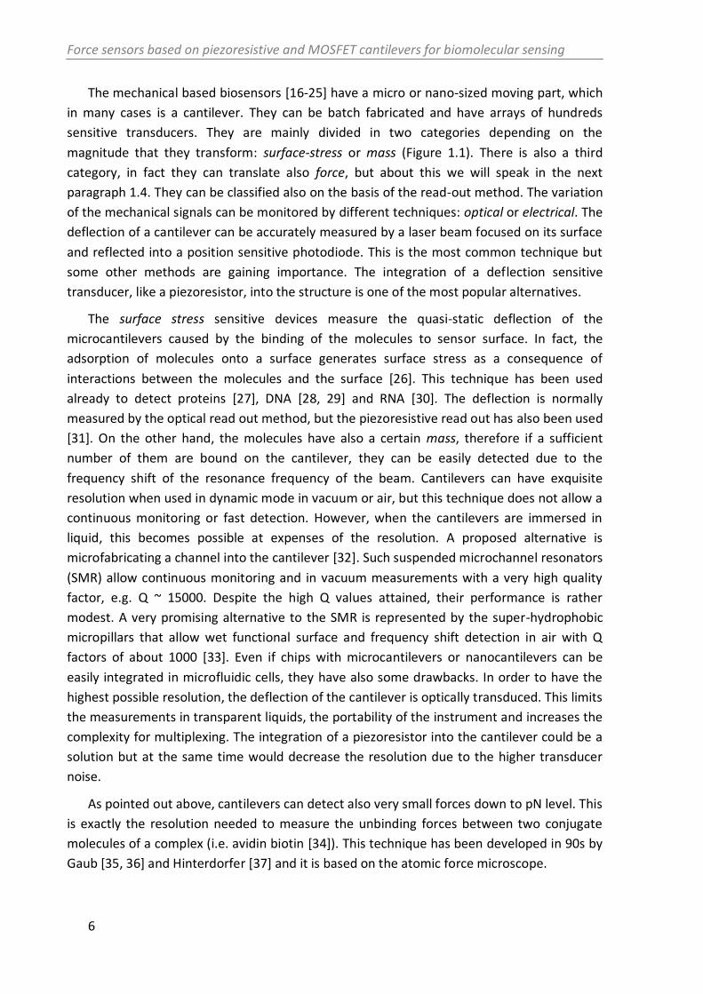
The mechanical based biosensors [16-25] have a micro or nano-sized moving part, which
in many cases is a cantilever. They can be batch fabricated and have arrays of hundreds
sensitive transducers. They are mainly divided in two categories depending on the
magnitude that they transform: surface-stress or mass (Figure 1.1). There is also a third
category, in fact they can translate also force, but about this we will speak in the next
paragraph 1.4. They can be classified also on the basis of the read-out method. The variation
of the mechanical signals can be monitored by different techniques: optical or electrical. The
deflection of a cantilever can be accurately measured by a laser beam focused on its surface
and reflected into a position sensitive photodiode. This is the most common technique but
some other methods are gaining importance. The integration of a deflection sensitive
transducer, like a piezoresistor, into the structure is one of the most popular alternatives.
The surface stress sensitive devices measure the quasi-static deflection of the
microcantilevers caused by the binding of the molecules to sensor surface. In fact, the
adsorption of molecules onto a surface generates surface stress as a consequence of
interactions between the molecules and the surface [26]. This technique has been used
already to detect proteins [27], DNA [28, 29] and RNA [30]. The deflection is normally
measured by the optical read out method, but the piezoresistive read out has also been used
[31]. On the other hand, the molecules have also a certain mass, therefore if a sufficient
number of them are bound on the cantilever, they can be easily detected due to the
frequency shift of the resonance frequency of the beam. Cantilevers can have exquisite
resolution when used in dynamic mode in vacuum or air, but this technique does not allow a
continuous monitoring or fast detection. However, when the cantilevers are immersed in
liquid, this becomes possible at expenses of the resolution. A proposed alternative is
microfabricating a channel into the cantilever [32]. Such suspended microchannel resonators
(SMR) allow continuous monitoring and in vacuum measurements with a very high quality
factor, e.g. Q ~ 15000. Despite the high Q values attained, their performance is rather
modest. A very promising alternative to the SMR is represented by the super-hydrophobic
micropillars that allow wet functional surface and frequency shift detection in air with Q
factors of about 1000 [33]. Even if chips with microcantilevers or nanocantilevers can be
easily integrated in microfluidic cells, they have also some drawbacks. In order to have the
highest possible resolution, the deflection of the cantilever is optically transduced. This limits
the measurements in transparent liquids, the portability of the instrument and increases the
complexity for multiplexing. The integration of a piezoresistor into the cantilever could be a
solution but at the same time would decrease the resolution due to the higher transducer
noise.
As pointed out above, cantilevers can detect also very small forces down to pN level. This
is exactly the resolution needed to measure the unbinding forces between two conjugate
molecules of a complex (i.e. avidin biotin [34]). This technique has been developed in 90s by
Gaub [35, 36] and Hinterdorfer [37] and it is based on the atomic force microscope.

Chapter I. Introduction
7
Figure 1.1. A) Cantilever as surface stress transducer: the ligands (red) attach to the receptors (green)
provoke a bending in the cantilever (z) and a surface stress. B) Cantilever as mass transducer: after
the binding of the ligands, the resonance frequency changes from f0 to f0-f.
1.4 – Atomic force spectroscopy in biomolecule recognition
The atomic force microscope (AFM) uses a microcantilever to measure the surface of a
sample with nanometer precision. The cantilever, usually made of silicon or silicon nitride,
has a sharp tip in its end with a radius of curvature of some nanometers. The cantilever or
the sample is mounted on a piezoelectric actuator that allows positioning in the 3
dimensions with sub-nanometric resolution. When the tip is brought in close proximity to
the sample surface, the interaction forces between the tip and the sample deflect the
cantilever. The probe scans the sample to create an image of its surface. To measure the
deflection of the cantilever, a laser is focused and reflected by the cantilever to a position
sensitive photodiode [38]. Knowing the cantilever spring constant, kC, the deflection, can
be converted into force by the Hooke’s law:
(1.1)
AFM has two main operating modes to create images: contact mode and dynamic mode.
In the contact mode, or static mode, the tip is brought in contact to the samples with a
certain force that is maintained during the raster scan. On the other hand, during the
scanning in dynamic mode, the cantilever is oscillating near its resonant frequency with
constant amplitude.
The AFM can be used also as a tool for measuring forces down to some pN [39], in the
modality usually called atomic force spectroscopy, AFS [34, 40, 41]. In this mode, the tip is
moved in the z vertical direction downwards and upwards with a constant speed and at a
fixed location on the x-y plane (Figure 1.2). At the same time, the deflection of the cantilever
B) A)
Force sensors based on piezoresistive and MOSFET cantilevers for biomolecular sensing
8
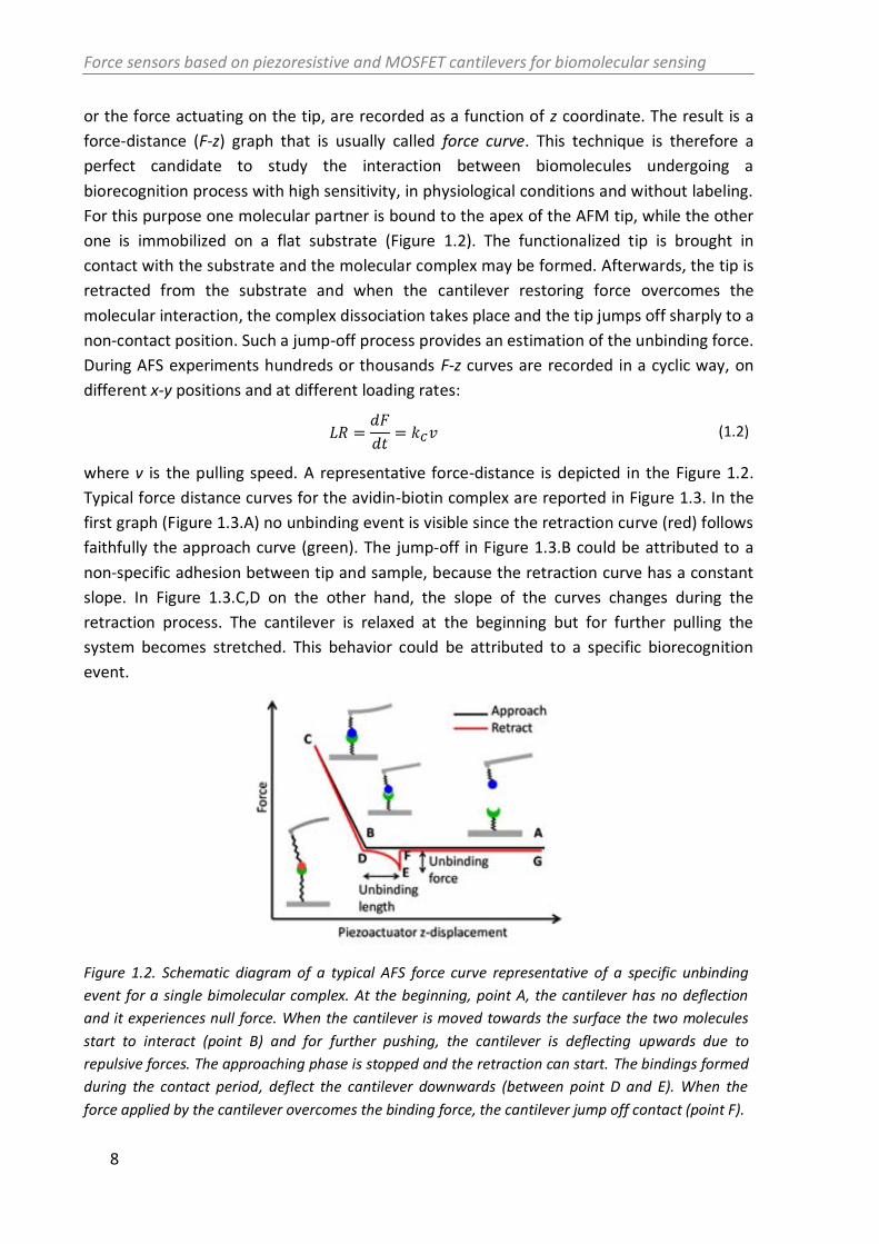
or the force actuating on the tip, are recorded as a function of z coordinate. The result is a
force-distance (F-z) graph that is usually called force curve. This technique is therefore a
perfect candidate to study the interaction between biomolecules undergoing a
biorecognition process with high sensitivity, in physiological conditions and without labeling.
For this purpose one molecular partner is bound to the apex of the AFM tip, while the other
one is immobilized on a flat substrate (Figure 1.2). The functionalized tip is brought in
contact with the substrate and the molecular complex may be formed. Afterwards, the tip is
retracted from the substrate and when the cantilever restoring force overcomes the
molecular interaction, the complex dissociation takes place and the tip jumps off sharply to a
non-contact position. Such a jump-off process provides an estimation of the unbinding force.
During AFS experiments hundreds or thousands F-z curves are recorded in a cyclic way, on
different x-y positions and at different loading rates:
(1.2)
where v is the pulling speed. A representative force-distance is depicted in the Figure 1.2.
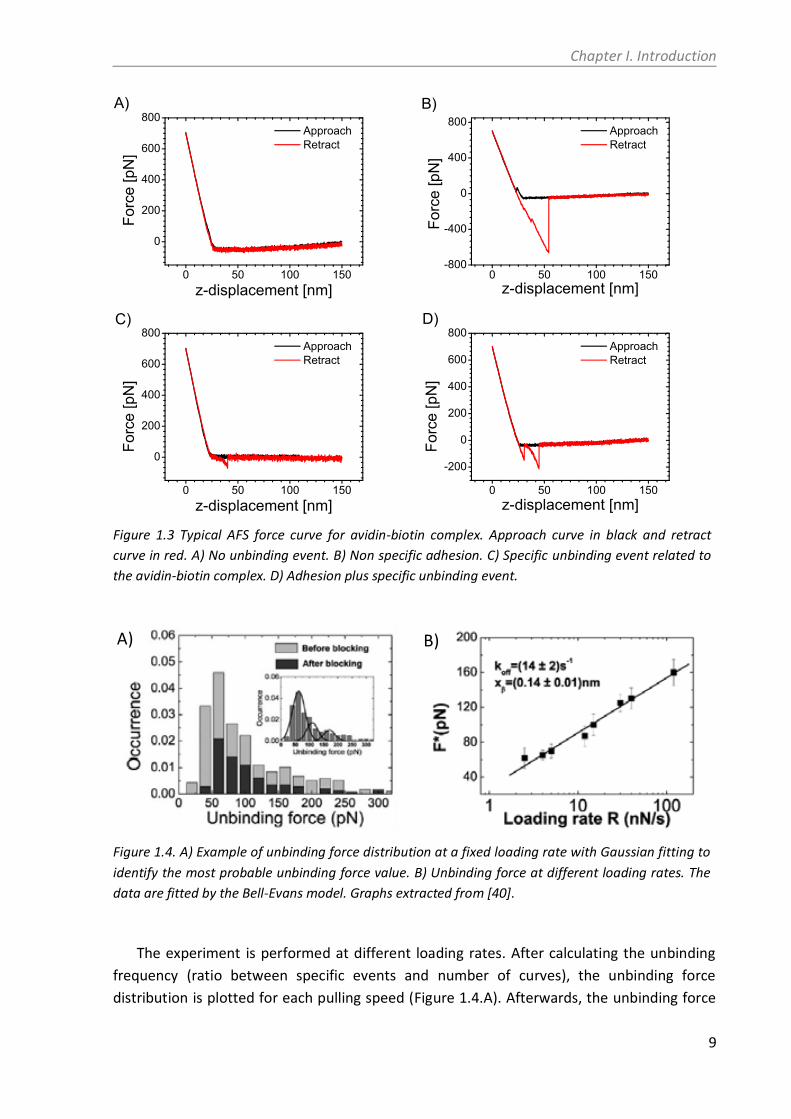
Typical force distance curves for the avidin-biotin complex are reported in Figure 1.3. In the
first graph (Figure 1.3.A) no unbinding event is visible since the retraction curve (red) follows
faithfully the approach curve (green). The jump-off in Figure 1.3.B could be attributed to a
non-specific adhesion between tip and sample, because the retraction curve has a constant
slope. In Figure 1.3.C,D on the other hand, the slope of the curves changes during the
retraction process. The cantilever is relaxed at the beginning but for further pulling the
system becomes stretched. This behavior could be attributed to a specific biorecognition
event.
Figure 1.2. Schematic diagram of a typical AFS force curve representative of a specific unbinding
event for a single bimolecular complex. At the beginning, point A, the cantilever has no deflection
and it experiences null force. When the cantilever is moved towards the surface the two molecules
start to interact (point B) and for further pushing, the cantilever is deflecting upwards due to
repulsive forces. The approaching phase is stopped and the retraction can start. The bindings formed
during the contact period, deflect the cantilever downwards (between point D and E). When the
force applied by the cantilever overcomes the binding force, the cantilever jump off contact (point F).
Chapter I. Introduction
9
0 50 100 150
0
200
400
600
800 Approach Retract
Forc
e [p
N]
z-displacement [nm]
A)
0 50 100 150-800
-400
0
400
800B)
Forc
e [p
N]
z-displacement [nm]
Approach Retract
0 50 100 150
0
200
400
600
800C)
Forc
e [p
N]
z-displacement [nm]
Approach Retract
0 50 100 150
-200
0
200
400
600
800D)
Forc
e [p
N]
z-displacement [nm]
Approach Retract
Figure 1.3 Typical AFS force curve for avidin-biotin complex. Approach curve in black and retract
curve in red. A) No unbinding event. B) Non specific adhesion. C) Specific unbinding event related to
the avidin-biotin complex. D) Adhesion plus specific unbinding event.
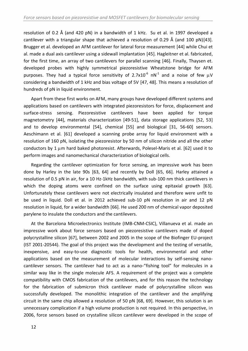
Figure 1.4. A) Example of unbinding force distribution at a fixed loading rate with Gaussian fitting to
identify the most probable unbinding force value. B) Unbinding force at different loading rates. The
data are fitted by the Bell-Evans model. Graphs extracted from [40].
The experiment is performed at different loading rates. After calculating the unbinding
frequency (ratio between specific events and number of curves), the unbinding force
distribution is plotted for each pulling speed (Figure 1.4.A). Afterwards, the unbinding force
B) A)

Force sensors based on piezoresistive and MOSFET cantilevers for biomolecular sensing
10
is extracted from the distribution and plotted against the loading rate (Figure 1.4.B). Using
the Bell-Evans model [40]:
(1.3)
to fit the graph in Figure 1.4.B it is possible to extract information on the equilibrium
properties of the molecular complex like its dissociation rate, koff, at zero pulling force and
the reaction coordinate corresponding to the separation between the bound and transition
state , xFigure 1.5.
Despite its very high force sensitivity, the AFM has still not become an analytical
instrument for detecting single molecules in different specimens such as blood, tissues or
cells. This is mainly due to the complexity of the instrument and of its use. Although the
transduction optical system has very high resolution, down to Å level and few pN, it makes
the AFM unfit to be used in the opaque fluids and introduces many laborious actions, which
slow down considerably the detection process. Moreover the AFM can hardly be integrated
into microfluidic cells and lacks in multiplexing and automation potentiality.
Figure 1.5. Energy diagram of a biomolecular complex. Upon an application of a force the energy
state shift towards lower values (dashed line). Graphs extracted from [40].
1.5 – Sensor requirements
In this section we will discuss about the requirements of the new diagnostic tool and
about the performance and design of the force probes, which is the principal part. The new
diagnostic device should:
Be for near patient testing or point of care testing. It should not require special
sample preparation and offer fast response time.
Be small in size
Have high sensitivity and selectivity

Chapter I. Introduction
11
Have high reliability
Multi-diagnosis (multiplexing) capability
Be for liquid and opaque sample analysis
Have no labeling need
As we saw in the previous sections, a very powerful method to detect a biomolecule is to
detect the intermolecular force between the molecule under investigation and its conjugate
molecule. This can offer much higher resolution than “traditional” methods like the
detection of the surface stress or the detection of the molecules mass. As we pointed out
before a candidate could be the AFM but has many intrinsic problems: it is unfit to be used
with opaque fluids, necessitate of many laborious actions and it doesn’t have multiplexing
potentiality. A self-sensing cantilever, a cantilever with an integrated deflection transducer
(i.e. a piezoresistor), could solve many problems that the AFM has. It wouldn’t necessitate a
laser and a photodetector and therefore it could work in opaque media. It would reduce
laborious processes like the alignment of the laser and of the photodetector that slow down
the analysis process. The chip could be integrated into a microfluidic system and therefore
the functionalization of the surfaces would be faster and easier. It would have multiplexing
potentiality because the chips could have arrays of hundreds of cantilevers.
On the other hand passing from an optical to and electrical read-out method can lead to
a decrease in resolution and have problems in liquid environment. In this perspective, the
probes have to be scaled down, especially in the thickness, to have a resolution similar to
the one of the AFM (few pN) and all the conductive parts of the chip have to be electrically
insulated. Moreover the probes should allow sensing frequencies up to 0.5-10 kHz. This
means that their resonance frequency should be equal or higher than these values. In fact,
typical AFS experiments are done at 0.1-1 seconds time scale, but the sampling frequency of
the force acting on the cantilever tip is between 0.5 and 10 kHz. This frequency is needed to
avoid the time average during the jump-off-contact.
1.6 – Piezoresistive cantilevers
In this chapter we aim to summarize the most relevant literature information about
silicon cantilever with piezoresistive transduction (piezoresistor or MOSFET) that have been
developed in the last two decades and have been used for different applications.
One of the first and perhaps the best know application, of a piezoresistive cantilever, has
been the atomic force microscopy. Tortonese et al. in 1993 developed a p-doped
piezoresistive silicon cantilever, integrated in a ¼ active Wheatstone bridge, obtaining
atomic resolution images [42]. His best cantilever had a resolution of 0.1 Å (and 1 nN) in the
bandwidth from 10 Hz to 1 kHz. In 1995 Linnemann et al. developed a cantilever with a
complete Wheatstone bridge integrated into the cantilever. This solution allowed a
Force sensors based on piezoresistive and MOSFET cantilevers for biomolecular sensing
12
resolution of 0.2 Å (and 420 pN) in a bandwidth of 1 kHz. Su et al. in 1997 developed a
cantilever with a triangular shape that achieved a resolution of 0.29 Å (and 100 pN)[43].
Brugger et al. developed an AFM cantilever for lateral force measurement [44] while Chui et
al. made a dual axis cantilever using a sidewall implantation [45]. Hagleitner et al. fabricated,
for the first time, an array of two cantilevers for parallel scanning [46]. Finally, Thaysen et.
developed probes with highly symmetrical piezoresistive Wheatstone bridge for AFM
purposes. They had a typical force sensitivity of 2.7x10⁻⁶ nN-1 and a noise of few V
considering a bandwidth of 1 kHz and bias voltage of 5V [47, 48]. This means a resolution of
hundreds of pN in liquid environment.
Apart from these first works on AFM, many groups have developed different systems and
applications based on cantilevers with integrated piezoresistors for force, displacement and
surface-stress sensing. Piezoresistive cantilevers have been applied for torque
magnetometry [44], materials characterization [49-51], data storage applications [52, 53]
and to develop environmental [54], chemical [55] and biological [31, 56-60] sensors.
Aeschimann et al. [61] developed a scanning probe array for liquid environment with a
resolution of 160 pN, isolating the piezoresistor by 50 nm of silicon nitride and all the other
conductors by 1 m hard baked photoresist. Afterwards, Polesel-Maris et al. [62] used it to
perform images and nanomechanical characterization of biological cells.
Regarding the cantilever optimization for force sensing, an impressive work has been
done by Harley in the late 90s [63, 64] and recently by Doll [65, 66]. Harley attained a
resolution of 0.5 pN in air, for a 10 Hz-1kHz bandwidth, with sub-100 nm thick cantilevers in
which the doping atoms were confined on the surface using epitaxial growth [63].
Unfortunately these cantilevers were not electrically insulated and therefore were unfit to
be used in liquid. Doll et al. in 2012 achieved sub-10 pN resolution in air and 12 pN
resolution in liquid, for a wider bandwidth [66]. He used 200 nm of chemical vapor deposited
parylene to insulate the conductors and the cantilevers.
At the Barcelona Microelectronics Institute (IMB-CNM-CSIC), Villanueva et al. made an
impressive work about force sensors based on piezoresistive cantilevers made of doped
polycrystalline silicon [67], between 2002 and 2005 in the scope of the Biofinger EU-project
(IST 2001-20544). The goal of this project was the development and the testing of versatile,
inexpensive, and easy-to-use diagnostic tools for health, environmental and other
applications based on the measurement of molecular interactions by self-sensing nano-
cantilever sensors. The cantilever had to act as a nano-“fishing tool” for molecules in a
similar way like in the single molecule AFS. A requirement of the project was a complete
compatibility with CMOS fabrication of the cantilevers, and for this reason the technology
for the fabrication of submicron thick cantilever made of polycrystalline silicon was
successfully developed. The monolithic integration of the cantilever and the amplifying
circuit in the same chip allowed a resolution of 50 pN [68, 69]. However, this solution is an
unnecessary complication if a high volume production is not required. In this perspective, in
2006, force sensors based on crystalline silicon cantilever were developed in the scope of
Chapter I. Introduction
13
Spanish national projects. Due to the higher piezoresistive coefficient of the crystalline
silicon, the sensor achieved a resolution of 65 pN with no amplification [70]. It has to be
pointed out that these resolutions were measured in air.
The integration of a transistor into a cantilever is relatively a newer idea and it has been
less exploited. Also in this case, one of the first applications has been the AFM. Akiyama et
al. in 1998 developed a cantilever with an embedded p-MOSFET transistor for scanning force
microscopy application [71]. Two years later, he integrated in the same chip an array of two
self-sensing and thermally actuated cantilevers and the amplifying circuit [72]. In 2006
Shekhawat et al. developed a biomolecular sensor based on n-MOSFET-embedded
microcantilevers [73]. He successfully detected low concentrations of avidin and goat
antibody molecules and the results indicated that the sensitivity was comparable to the
traditional optical transduction. Tark in 2009 [74] and Singh in 2011 [75], explored different
p- and n-MOSFET cantilever designs. In the same years, Wang developed a sensor for
observing the kinetics of chemical molecule interaction based on n-MOSFET cantilever [76,
77].
1.7 – Thesis outline
The following chapters are organized as follows:
Chapter 2 – Theoretical background. In this chapter, the fundamentals of the
linear elasticity theory, of the piezoresistive effect and of the noise in the
electronic devices are discussed. These theories are at the basis of the analytical
model of the piezoresistive cantilever.
Chapter 3 – Piezoresistive cantilever. The electromechanical model that we used
to optimize the resolution of the force sensor is presented. The mask design, the
process fabrication and the fabrication issues of the piezoresistive force probes
are also discussed. Afterwards, the development of new on-wafer
characterization set-ups and techniques, fundamental for reliable and fast
measurements, will be described. Finally, the mechanical, electrical and
electromechanical performance of the different force probes will be reported.
Chapter 4 – MOSFET cantilever. We will present the model, the mask design, the
fabrication process and the characterization of the second option of force sensor:
a cantilever with integrated a piezosensitive MOSFET.
Chapter 5 – Biomolecule recognition. In order to perform biomolecule
recognition experiments, we integrated the piezoresistive sensor into a
commercial AFM to take advantage of the high stability of this equipment and
highly reliable displacement of the piezo-actuator. In this chapter we will discuss
the mechanical and electrical integration of the sensor into the AFM. The system
Force sensors based on piezoresistive and MOSFET cantilevers for biomolecular sensing
14
achieved a 10-pN resolution, which allowed us to detect biorecognition specific
events underlying the biotin-avidin complex formation.
Chapter 6 – Summary. We will highlight the most important results of the work
and give suggestions for future research directions
All the research work presented in this thesis has been developed in the scope of three
Spanish projects supported by the Spanish Ministry of Science and Innovation: TEC2007-
65692, TEC2011-23600, NANOSELECT-CSD2007- 38400041 (Consolider-Ingenio 2010
Programme).
The scientific short stay at the Biophysics and Nanoscience center of the University of
Viterbo has been supported by the EU commission through the COST ACTION TD-1002
(AFM4NANOMED&BIO) (chapter 5). The work made during this collaboration has been partly
supported by the PRIN-MIUR project n°2009 WPZM4S and by AIRC (Grant IG10412).

Chapter I. Introduction
15
References
1. Crook, M.A., Near patient testing and pathology in the new millennium. Journal of clinical pathology, 2000. 53(1): p. 27-30.
2. Jain, K.K., Nanobiotechnology and personalized medicine, in The Handbook of Nanomedicine2012, Springer. p. 451-454.
3. Cheng, M.M.C., et al., Nanotechnologies for biomolecular detection and medical diagnostics. Current Opinion in Chemical Biology, 2006. 10(1): p. 11-19.
4. Ferrari, M., Cancer nanotechnology: Opportunities and challenges. Nature Reviews Cancer, 2005. 5(3): p. 161-171.
5. Ferrari, M. and A.P. Lee, BioMEMS and biomedical nanotechnology. Vol. 21. 2006: Springer.
6. Craighead, H., Future lab-on-a-chip technologies for interrogating individual molecules. Nature, 2006. 442(7101): p. 387-393.
7. Wilchek, M., E.A. Bayer, and O. Livnah, Essentials of biorecognition: the (strept) avidin-biotin system as a model for protein-protein and protein-ligand interaction. Immunology letters, 2006. 103(1): p. 27-32.
8. Badis, G., et al., Diversity and complexity in DNA recognition by transcription factors. Science, 2009. 324(5935): p. 1720-1723.
9. Baszkin, A. and W. Norde, Physical chemistry of biological interfaces1999: CRC Press. 10. Lawrence, M.B. and T.A. Springer, Leukocytes roll on a selectin at physiologic flow rates:
distinction from and prerequisite for adhesion through integrins. Cell, 1991. 65(5): p. 859-873.
11. Coussens, L.M. and Z. Werb, Inflammatory Cells and Cancer Think Different! The Journal of experimental medicine, 2001. 193(6): p. F23-F26.
12. O'Byrne, K.J. and A.G. Dalgleish, Chronic immune activation and inflammation as the cause of malignancy. British Journal of Cancer, 2001. 85(4): p. 473.
13. Turner, A.P.F., Biosensors: sense and sensibility. Chemical Society Reviews, 2013. 42(8): p. 3184-3196.
14. Yang, Y.T., et al., Zeptogram-scale nanomechanical mass sensing. Nano Letters, 2006. 6(4): p. 583-586.
15. Lassagne, B., et al., Ultrasensitive mass sensing with a nanotube electromechanical resonator. Nano Letters, 2008. 8(11): p. 3735-3738.
16. Arlett, J.L., E.B. Myers, and M.L. Roukes, Comparative advantages of mechanical biosensors. Nature Nanotechnology, 2011. 6(4): p. 203-215.
17. Boisen, A. and T. Thundat, Design & fabrication of cantilever array biosensors. Materials Today, 2009. 12(9): p. 32-38.
18. Boisen, A., et al., Cantilever-like micromechanical sensors. Reports on Progress in Physics, 2011. 74(3): p. 036101.
19. Datar, R., et al., Cantilever sensors: nanomechanical tools for diagnostics. Mrs Bulletin, 2009. 34(06): p. 449-454.
20. Fritz, J.r., Cantilever biosensors. Analyst, 2008. 133(7): p. 855-863. 21. Raiteri, R., et al., Micromechanical cantilever-based biosensors. Sensors and Actuators,
B: Chemical, 2001. 79(2-3): p. 115-126.

Force sensors based on piezoresistive and MOSFET cantilevers for biomolecular sensing
16
22. Waggoner, P.S. and H.G. Craighead, Micro- and nanomechanical sensors for environmental, chemical, and biological detection. Lab on a Chip, 2007. 7(10): p. 1238-1255.
23. Hansen, K.M. and T. Thundat, Microcantilever biosensors. Methods, 2005. 37(1): p. 57-64.
24. Goeders, K.M., J.S. Colton, and L.A. Bottomley, Microcantilevers: sensing chemical interactions via mechanical motion. Chemical reviews, 2008. 108(2): p. 522.
25. Tamayo, J., et al., Biosensors based on nanomechanical systems. Chemical Society Reviews, 2013. 42(3): p. 1287-1311.
26. Godin, M., et al., Cantilever-based sensing: the origin of surface stress and optimization strategies. Nanotechnology, 2010. 21(7): p. 075501.
27. Backmann, N., et al., A label-free immunosensor array using single-chain antibody fragments. Proceedings of the National Academy of Sciences of the United States of America, 2005. 102(41): p. 14587-14592.
28. Wu, G., et al., Bioassay of prostate-specific antigen (PSA) using microcantilevers. Nature biotechnology, 2001. 19(9): p. 856-860.
29. Mertens, J., et al., Label-free detection of DNA hybridization based on hydration-induced tension in nucleic acid films. Nature Nanotechnology, 2008. 3(5): p. 301-307.
30. Zhang, J., et al., Rapid and label-free nanomechanical detection of biomarker transcripts in human RNA. Nature Nanotechnology, 2006. 1(3): p. 214-220.
31. Rasmussen, P.A., et al., Optimised cantilever biosensor with piezoresistive read-out. Ultramicroscopy, 2003. 97(1-4): p. 371-376.
32. Burg, T.P., et al., Weighing of biomolecules, single cells and single nanoparticles in fluid. Nature, 2007. 446(7139): p. 1066-1069.
33. Melli, M., G. Scoles, and M. Lazzarino, Fast Detection of Biomolecules in Diffusion-Limited Regime Using Micromechanical Pillars. ACS nano, 2011. 5(10): p. 7928-7935.
34. Bizzarri, A.R., Cannistraro, S., Dynamic Force Spectroscopy and Biomolecular Recognition2012: CRC Press, Boca Raton.
35. Florin, E.L., V.T. Moy, and H.E. Gaub, Adhesion forces between individual ligand-receptor pairs. Science, 1994. 264(5157): p. 415-417.
36. Moy, V.T., E.-L. Florin, and H.E. Gaub, Intermolecular forces and energies between ligands and receptors. Science, 1994: p. 257-257.
37. Hinterdorfer, P., et al., Detection and localization of individual antibody-antigen recognition events by atomic force microscopy. Proceedings of the National Academy of Sciences of the United States of America, 1996. 93(8): p. 3477-3481.
38. Meyer, G. and N.M. Amer, Novel optical approach to atomic force microscopy. Applied Physics Letters, 1988. 53(12): p. 1045-1047.
39. Junker, J.P., F. Ziegler, and M. Rief, Ligand-Dependent Equilibrium Fluctuations of Single Calmodulin Molecules. Science, 2009. 323(5914): p. 633-637.
40. Bizzarri, A.R. and S. Cannistraro, The application of atomic force spectroscopy to the study of biological complexes undergoing a biorecognition process. Chemical Society Reviews, 2010. 39(2): p. 734-749.
41. Hinterdorfer, P. and Y.F. Dufrene, Detection and localization of single molecular recognition events using atomic force microscopy. Nature Methods, 2006. 3(5): p. 347-355.

Chapter I. Introduction
17
42. Tortonese, M., R.C. Barrett, and C.F. Quate, Atomic resolution with an atomic force microscope using piezoresistive detection. Applied Physics Letters, 1993. 62(8): p. 834-836.
43. Su, Y., et al., Fabrication of improved piezoresistive silicon cantilever probes for the atomic force microscope. Sensors and Actuators A: Physical, 1997. 60(1-3): p. 163-167.
44. Brugger, J., et al., Microfabricated ultrasensitive piezoresistive cantilevers for torque magnetometry. Sensors and Actuators A: Physical, 1999. 73(3): p. 235-242.
45. Chui, B.W., et al., Independent detection of vertical and lateral forces with a sidewall-implanted dual-axis piezoresistive cantilever. Applied Physics Letters, 1998. 72(11): p. 1388-1390.
46. Hagleitner, C., et al. On-chip circuitry for a CMOS parallel scanning AFM. in 1999 Symposium on Smart Structures and Materials. 1999. International Society for Optics and Photonics.
47. Jacob, T., Cantilever for bio-chemical sensing integrated in a microliquid handling system, 2001, Technical University of Denmark.
48. Thaysen, J., et al., Atomic force microscopy probe with piezoresistive read-out and a highly symmetrical Wheatstone bridge arrangement. Sensors and Actuators A: Physical, 2000. 83(1-3): p. 47-53.
49. Pruitt, B.L. and T.W. Kenny, Piezoresistive cantilevers and measurement system for characterizing low force electrical contacts. Sensors and Actuators A: Physical, 2003. 104(1): p. 68-77.
50. Seel, S.C. and C.V. Thompson, Piezoresistive microcantilevers for in situ stress measurements during thin film deposition. Review of scientific instruments, 2005. 76(7): p. 075103-075103-8.
51. Peiner, E., M. Balke, and L. Doering, Form measurement inside fuel injector nozzle spray holes. Microelectronic Engineering, 2009. 86(4-6): p. 984-986.
52. Chui, B.W., et al., Low-stiffness silicon cantilevers with integrated heaters and piezoresistive sensors for high-density AFM thermomechanical data storage. Microelectromechanical Systems, Journal of, 1998. 7(1): p. 69-78.
53. Ried, R.P., et al., 6-mhz 2-N/m piezoresistive atomic-force microscope cantilevers with incisive tips. Microelectromechanical Systems, Journal of, 1997. 6(4): p. 294-302.
54. Boisen, A., et al., Environmental sensors based on micromachined cantilevers with integrated read-out. Ultramicroscopy, 2000. 82(1-4): p. 11-16.
55. Jensenius, H., et al., A microcantilever-based alcohol vapor sensor-application and response model. Applied Physics Letters, 2000. 76(18): p. 2615-2617.
56. Baselt, D.R., et al., A high-sensitivity micromachined biosensor. Proceedings of the IEEE, 1997. 85(4): p. 672-679.
57. Marie, R., et al., Adsorption kinetics and mechanical properties of thiol-modified DNA-oligos on gold investigated by microcantilever sensors. Ultramicroscopy, 2002. 91(1-4): p. 29-36.
58. Yang, M., et al., High sensitivity piezoresistive cantilever design and optimization for analyte-receptor binding. Journal of Micromechanics and Microengineering, 2003. 13(6): p. 864.
59. Wee, K.W., et al., Novel electrical detection of label-free disease marker proteins using piezoresistive self-sensing micro-cantilevers. Biosensors and Bioelectronics, 2005. 20(10): p. 1932-1938.

Force sensors based on piezoresistive and MOSFET cantilevers for biomolecular sensing
18
60. Na, K.-H., Y.-S. Kim, and C.J. Kang, Fabrication of piezoresistive microcantilever using surface micromachining technique for biosensors. Ultramicroscopy, 2005. 105(1): p. 223-227.
61. Aeschimann, L., et al., Scanning probe arrays for life sciences and nanobiology applications. Microelectronic Engineering, 2006. 83(4-9): p. 1698-1701.
62. Polesel-Maris, J., et al., Piezoresistive cantilever array for life sciences applications, in Proceedings of the International Conference on Nanoscience and Technology2007. p. 955-959.
63. Harley, J.A. and T.W. Kenny, High-sensitivity piezoresistive cantilevers under 1000 Å thick. Applied Physics Letters, 1999. 75(2): p. 289-291.
64. Harley, J.A., Advances in Piezoresistive Probes for Atomic Force Microscope, 2000, Stanford University.
65. Doll, J.C., Advances in high bandwidth nanomechanical force sensors with integrated actuation, 2012, Stanford University.
66. Doll, J.C. and B.L. Pruitt, High-bandwidth piezoresistive force probes with integrated thermal actuation. Journal of Micromechanics and Microengineering, 2012. 22(9): p. 095012.
67. Villanueva, L.G., Development of Cantilevers for Biomolecular Measurements, 2006, Universitat Autonoma de Barcelona.
68. Villanueva, G., et al., Piezoresistive cantilevers in a commercial CMOS technology for intermolecular force detection. Microelectronic Engineering, 2006. 83(4-9): p. 1302-1305.
69. Villanueva, G., et al., Submicron piezoresistive cantilevers in a CMOS-compatible technology for intermolecular force detection. Microelectronic Engineering, 2004. 73-4: p. 480-486.
70. Villanueva, G., et al., Crystalline silicon cantilevers for piezoresistive detection of biomolecular forces. Microelectronic Engineering, 2008. 85(5-6): p. 1120-1123.
71. Akiyama, T., et al., Characterization of an integrated force sensor based on a MOS transistor for applications in scanning force microscopy. Sensors and Actuators A: Physical, 1998. 64(1): p. 1-6.
72. Akiyama, T., et al., Integrated atomic force microscopy array probe with metal-oxide-semiconductor field effect transistor stress sensor, thermal bimorph actuator, and on-chip complementary metal-oxide-semiconductor electronics. Journal of Vacuum Science & Technology B, 2000. 18(6): p. 2669-2675.
73. Shekhawat, G., S.H. Tark, and V.P. Dravid, MOSFET-embedded microcantilevers for measuring deflection in biomolecular sensors. Science, 2006. 311(5767): p. 1592-1595.
74. Tark, S.-H., et al., Nanomechanoelectronic signal transduction scheme with metal-oxide-semiconductor field-effect transistor-embedded microcantilevers. Applied Physics Letters, 2009. 94(10): p. 104101-104101-3.
75. Singh, P., et al., Microcantilever sensors with embedded piezoresistive transistor read-out: Design and characterization. Sensors and Actuators A: Physical, 2011. 171(2): p. 178-185.
76. Wang, J., et al., 100 n-type metal-oxide-semiconductor field-effect transistor-embedded microcantilever sensor for observing the kinetics of chemical molecules interaction. Applied Physics Letters, 2009. 95: p. 124101.

Chapter I. Introduction
19
77. Wang, J., et al., Chemisorption sensing and analysis using silicon cantilever sensor based on n-type metal–oxide–semiconductor transistor. Microelectronic Engineering, 2011. 88(6): p. 1019-1023.
Force sensors based on piezoresistive and MOSFET cantilevers for biomolecular sensing
20

Chapter II. Theoretical background
21
Chapter II
2 – Theoretical background
Chapter 2 - Theoretical background 21
2.1 – Cantilever mechanics 23
2.1.1 – Mechanics of materials 23
2.1.2 – Loading, support and bending moment 27
2.1.3 – Curvature and beam equations 29
2.1.4 – Cantilever with constant cross section and homogeneous material 32
2.1.4.1 – Static deflection 32
2.1.4.2 – Resonance frequency 33
2.1.5 – Cantilever with a multilayer structure and variable cross section 34
2.1.5.1 – Static deflection 34
2.1.5.2 – Resonance frequency 36
2.2 – Piezoresistive effect 36
2.2.1 – Silicon piezoresistor 36
2.2.1.1 – Orientation, doping and temperature dependence 38
2.2.2 – Silicon MOSFET 40
2.2.2.1 – MOSFET model 41
2.2.2.2 – Piezoresistivity and carrier mobility enhancement in MOSFET transistors
43
2.2.2.3 – Orientation, doping, gate voltage, drain voltage, gate length and
temperature dependence 44
2.3 – Noise 49
2.3.1 – Silicon resistor. 49
2.3.1.1 – Thermal noise 50
2.3.1.2 – 1/f noise 50
2.3.2 – MOSFET 51
2.3.2.1 – Thermal noise 51
Force sensors based on piezoresistive and MOSFET cantilevers for biomolecular sensing
22
2.3.2.2 – 1/f noise 52
2.3.3 –Thermomechanical noise 53
References 55

Chapter II. Theoretical background
23
Theoretical background
In this chapter we will discuss the fundamentals of the linear elasticity theory especially
in the case of the cantilever beam (section 2.1). We will report also about the piezoresistive
effect in silicon for piezoresistors and MOSFET cases (section 2.2). In the third section
(section 2.3) the noise in the electronic devices will be introduced. These theories are at the
basis of the analytical model of the piezoresistive cantilever (chapter 3).
2.1 – Cantilever mechanics
2.1.1 – Mechanics of materials
Some basic concepts and definition about theory of the linear elasticity of the materials
will be here briefly reminded. More detailed treatises can be found in [1-3].
Let’s remind as first the concepts of stress, σ, and strain, ε, using a very simple example.
If a cylindrical bar is subjected to a direct pull or push along its axis as shown Figure 2.1 then
it is said to be subjected to tension (σ>0) or compression (σ<0) and it suffers elongation (ε>0)
or shortening (ε<0), respectively.
The stress is defined as the total force, F, actuating on the bar divided by the cross
sectional area, A, while the strain is defined as the change in length, δL, divided by the
original length, L. A material is said to be elastic if it returns to its original, unloaded
dimensions, when the load is removed. A particular form of elasticity which applies to a large
range of materials, at least over part of their load range, produces deformations, and strains,
which are proportional to the loads, and stresses. This proportionality is described by the
Hooke’s law and the coefficient of proportionality is the Young’s modulus, E (or modulus of
elasticity):
(2.1)
We can speak therefore about linear elasticity and this is true for small displacements.
Moreover a material which has a uniform structure throughout without any flaws or
discontinuities is termed a homogenous material. Inhomogeneous materials have
mechanical characteristics that vary from point to point. If a material exhibits uniform
properties throughout in all directions it is said to be isotropic, conversely one which does
not exhibit this uniform behavior is said to be anisotropic. Just to fix the ideas the crystalline
silicon is homogeneous and anisotropic.
Let’s now consider a general three dimensional case: an infinitesimal cube of material
subjected to a general load condition (Figure 2.2).

Force sensors based on piezoresistive and MOSFET cantilevers for biomolecular sensing
24
Figure 2.1. On the left: bar, with a cross-section A, subjected to tension and compression by a force F.
On the right: bar subjected to tension showing the deformation, L, and unloaded bar with original
length, L.
Figure 2.2. Infinitesimal cube of material under stress and fully described by normal () and shear ()
stresses.
In this case the stressed material is fully described by the stress matrix:
(2.2)
The first position of the sub index refers to the surface normal upon which the stress acts
and the second one refers to the direction of the stress component. Therefore σxx (written
also σx) is the normal stress on the surface with the normal x acting in x direction while τxy
(or σxy) is the shear stress acting on the surface with the normal x in the y direction and, by
the way, it is possible to demonstrate that τxy= τyx, having a symmetric matrix. These stresses
provoke related displacements and therefore strain is fully described by the strain matrix:
(2.3)
If we consider for one moment just the x direction, all the points in the x direction are
deformed and described by a displacement u (Figure 2.3).

Chapter II. Theoretical background
25
Figure 2.3. The displacement vector u(x,y,z) causes a deformation in x direction. The other two
vectors v(x,y,z) and w(x,y,z) cause deformation in y and z directions respectively.
Therefore we can define the normal displacement εxx (written also εx) as:
(2.4)
In general the displacement of one point P to P’ in the body is described by one vector r
with the 3 components u, v and w in the directions x, y and z respectively. The components
u, v and w depend on the three coordinates:
u=u(x,y,z) ; v=v(x,y,z) ; w=w(x,y,z) (2.5)
Now we can define the shear strain, εxy for example, as:
(2.6)
And the engineering shear strain:
(2.7)
Also in this case it is possible to demonstrate that xy=yx (symmetric matrix). Now, when
the infinitesimal cube of material is stressed, let’s say just in x direction, it presents a shrink
in the other two direction y and z that are proportional to x, if we are considering isotropic
material:
(2.8)
is called Poisson’s coefficient. Concluding, one infinitesimal cube of isotropic material
under general load condition determines the following strain values:
(2.9a)
(2.9b)
(2.9c)

Force sensors based on piezoresistive and MOSFET cantilevers for biomolecular sensing
26
Where G is the shear modulus:
(2.10)
In the case of an anisotropic material the things are more complicated and for a general
load case we must write:
(2.11)
Or:
(2.12)
And
(2.13)
The stiffness matrix is traditionally represented by the symbol C, while S is reserved for the
compliance matrix. This convention may seem backwards, but perception is not always
reality. For cubic materials, like the silicon is, there are just three independent elastic
constants:
(2.14a)
(2.14b)
(2.14c)
And all the other constants are zero. Therefore the stiffness matrix becomes:
(2.15)
In the case of the silicon on the plane (100) the three constants are C11=166 GPa, C12=64 Gpa
and C44=80 Gpa [4]. From these values it is possible to calculate the Young’s modulus,
Poisson’s ratio and shear modulus for different crystalline directions (Table 2.1, Figure 2.4):

Chapter II. Theoretical background
27
Direction Expression Value [Gpa]
[100]
130
[110]
170
[111]
189
Table 2.1. Young’s moduli expressions for the most common silicon crystallographic directions.
Figure 2.4. Young’s modulus (x1011 Pa) (left), Poisson’s ratio (center) and shear modulus (x1011 Pa)
(right) calculated values for silicon in the (100) plane. [4]
2.1.2 – Loading, support and bending moment
In order to introduce the basic concepts as loads, supports and bending moments let’s
consider the simplest mechanical element: the beam. The beam can be subjected (Figure
2.5) to point forces, F (ideally are forces that are applied on one infinitesimal point of the
surface), distributed load, Q (pressure, weight) and concentrated moments, M.
The boundary conditions, which avoid the beam to translate or rotate, are called
supports and there are basically three types (Figure 2.5): fixed or clamped (the beam can’t
translate or rotate), pinned (the beam can just rotate) and pinned on rollers (the beam can
translate and rotate but it is fixed on the surface).
In equilibrium the beam do not translate neither rotate, therefore the sums of the forces
and of the moments applied on the beam must be zero. Let’s consider as example one beam
with a fixed end: a cantilever beam (or simply cantilever). If it is at equilibrium, because of
the point force, F, at the fixed end there must be a force reaction, FR, and a moment
reaction, MR (Figure 2.6). In other words if the support doesn’t allow the translation, there
can be a force reaction and if doesn’t allowed rotation there can be a moment reaction.

Force sensors based on piezoresistive and MOSFET cantilevers for biomolecular sensing
28
Because of the equilibrium the total force, FT, and the total moment, MT, actuating on
the cantilever must be zero, therefore:
(total moment about support) (2.16)
(2.17)
Now, each segment of the beam must be also in equilibrium, therefore if we section the
beam at a certain length x, we have to suppose internal shear force (V) and internal bending
moment (M) (Figure 2.6). For the case of the cantilever we have
(2.18)
Let’s now consider just a differential beam element. It is convention to consider
moments and force positive (or negative) like it is depicted in the figure below (Figure 2.7).
Figure 2.5. On the left: representation of a point force (F), distributed load (Q) and concentrated
torque (M). On the right: representation of the boundary condition for a beam.
Figure 2.6. On the left: reactions of the clamped edge due to a force F actuating on one cantilever
beam. On the right: representation of internal reaction in a beam.

Chapter II. Theoretical background
29
Figure 2.7. Conventions used for moments and shears.
This differential beam subjected to all the loads (point loads, distributed loads and
moments), in equilibrium must obey governing differential equation for shear forces and
moments:
(2.19)
(2.20)
The change in the internal shear force is related to a distributed load and a change in
internal moment is related to the internal shear force.
2.1.3 – Curvature and beam equations
In the previous paragraph we saw how the internal forces varies along the beam while in
this one we will take into consideration stress, strain and deformation of the beam and we
will see how they varies in its cross section.
Figure 2.8. A beam initially unstressed (left), the same beam subjected to a bending moment (centre)
and its cross sectional area.

Force sensors based on piezoresistive and MOSFET cantilevers for biomolecular sensing
30
If we now consider a beam initially unstressed and then subjected to a constant bending
moment along its length, i.e. pure bending, as would be obtained by applying equal moment
at each end, it will bend to a radius R as shown in (Figure 2.8). As a result of this bending the
top fibres of the beam will be subjected to tension (the fibres are elongated) and the bottom
to compression (the fibres are shortened). It is reasonable to suppose, therefore, that
somewhere between the two there are points at which the stress is zero (and the fibres have
the same length than before applying the moment). The locus of all such points is termed
neutral axis and it located where the centroid is located. The radius of curvature R is then
measured to this axis. For symmetrical sections the neutral axis is also the axis of symmetry
while if the beam has not a symmetrical cross section the centroid is calculated by:
(2.21)
The fibre AB, distant z from the neutral axis, is stretched to A’B’ if the bending moment is
applied. The strain of fibre AB, along the x direction, is defined as the elongation divided by
the original length:
(2.22)
Since AB=CD, and the neutral axis is not strained CD=C’D’
(2.23)
Therefore the stress in x direction increases linearly with the z direction being zero on the
neutral axis:
(2.24)
where E is the Young’s modulus.
On the strip of area, dA, of the cross section (Figure 2.8) is acting the force
(2.25)
and the moment about the neutral axis is:
(2.26)
Considering the whole cross section:
(2.27)
E and R are considered constant (independent of dA). The integral in the expression is called
second moment of area, it is calculated taking as origin of z coordinate the neutral axis, and
given the symbol I, therefore we can write:

Chapter II. Theoretical background
31
(2.28)
If the beam is of uniform section, from the previous equation we have that the radius of
curvature is constant if the material is homogeneous and we apply a constant bending
moment. The radius of curvature of the beam is:
(2.29)
and is related directly with the term EI bending stiffness (or flexural rigidity) which depends
on the Young’s modulus of the material and on the area and shape of the cross section. Here
we assumed the case of pure bending without any shear stress being present. In the most
practical beam loading cases shear and bending occurs together at most points, however it
would be possible to show that where the bending moment is maximum, in fact, the shear
stress is zero and that the bending moment produces by far the greatest magnitude of
stress.
Let’s find now the relationship between the curvature and the applied load. Consider a
beam AB (Figure 2.9) which is initially horizontal when unloaded. If this deflects to a new
position A’B’ under load, the slope at any point C is:
(2.30)
This is usually very small in practice, and for small curvatures is:
(2.31)
(2.32)
Figure 2.9. Representation of a beam initially unloaded (A-B) and after loading (A’-B’)

Force sensors based on piezoresistive and MOSFET cantilevers for biomolecular sensing
32
Therefore considering (2.30)
(2.33)
And considering the equation (2.29)
(2.34)
Remembering also the previous equation we can summarize:
Displacement (2.35)
Slope (2.36)
Bending moment (2.37)
Shear force (2.38)
Loading (2.39)
2.1.4 – Cantilever with constant cross section and homogeneous material
2.1.4.1 – Static deflection
Let’s now analyze the cantilever case (simple beam long L clamped at one end) with the transverse load, F, at its end (Figure 2.10). Considering the equations (2.18) and (2.37) we can write:
(2.40a)
(2.40b)
(2.40c)
Considering the boundary conditions at x=0 (in the origin the deflection is zero and the beam is parallel to the x direction) we can calculate the coefficients A and B:
(2.41a)
(2.41b)
Therefore the equation of the elastic curve (deflection of the neutral axis) is:

Chapter II. Theoretical background
33
(2.42)
where the bending stiffness is
(2.43)
Normally the end deflection of the cantilever is modelled as the deformation of a spring
with elastic constant k (Figure 2.10):
(2.44a)
(2.44b)
Finally considering the equations (2.23) and (2.33) we can write the strain and stress
formulas for this case:
(2.45a)
(2.45b)
Figure 2.10. Cantilever model: the cantilever subjected to a point force can be modelled by a spring
with constant k and mass m (left). On the right, the stress dependence on x and z axes is reported.
2.1.4.2 – Resonance frequency
Under the same conditions of linear elasticity and small deflection, the resonance
frequency of the firs mode of the cantilever beam, in vacuum, can be calculated by the
following formula [5]:
(2.46)
where m is the mass density of the material of the beam.

Force sensors based on piezoresistive and MOSFET cantilevers for biomolecular sensing
34
2.1.5 – Cantilever with a multilayer structure and variable cross section
2.1.5.1 – Static deflection
Not to be confounded with beam made up of composite material, this composite
(laminated) beam in this context refers to a beam with layering material having different
Young's moduli and each material homogeneous. The difference in moduli will result in a
beam having a shift in neutral axis under bending load. One way to work a composite beam
problem is by using an equivalent beam. The basic idea is to make a beam out of just one
material but expand or contract the substituted part laterally so that it has the same
functionality as the original beam (Figure 2.11).
From these considerations the position of neutral axis is:
(2.47)
where i refers to the layer, zt and zd refer to the top and to the bottom of the layer
respectively and E is the Young’s modulus. Now that the position of the neutral axis is
calculated it is possible to calculate the bending stiffness of the composite cantilever:
(2.48)
Concluding, the stress (discontinuous) and strain (continuous) (Figure 2.11) are given by:
(2.49a)
(2.49b)
Let’s now consider instead that the beam is single layered and has not a constant cross
section along the x direction like in the picture (Figure 2.12).
From the point of view of the displacement these two situations, U-cantilever or T
cantilever, have the same solution (if the cross-sectional area is the same). For the two parts,
1 and 2, of the cantilever we can write:
(2.50a)
(2.50b)

Chapter II. Theoretical background
35
Figure 2.11. Two-layers-beam made of two materials with Young’s moduli E1 and E2 and equivalent
beam made of a single material with Young’s modulus E. (left). On the right, representation of the x-
component of strain and stress dependence on z-direction.
Figure 2.12. Cantilever with non constant cross sectional area: U or T shaped cantilevers. The
cantilever can be modelled as two cantilevers in series. The first part [0,L1] has smaller cross sectional
area and lower bending stiffness. The second part [L1,L2] has bigger cross sectional area and higher
bending stiffness.
EI1 and EI2 are the bending stiffness (or flexural rigidity) of the beam in the two different
parts of the cantilever. These can be calculated from the previous equation (2.47-(2.48).
Now in L1 has to be 1=2 (the displacement has to be the same) and ’1=’2 (the tangent of
the displacement is the same too). From these two boundary conditions we obtain A and B:
(2.51a)

Force sensors based on piezoresistive and MOSFET cantilevers for biomolecular sensing
36
(2.51b)
Finally the spring constant of the cantilever is:
(2.52)
And stress and strain can be calculated as in the equation (2.49).
2.1.5.2 – Resonance frequency
Under the same assumptions, the resonance frequencies of a cantilever with non
constant cross section can be numerically calculated using the following formulas [5]:
(2.53)
(2.54)
Where =w1/w2 and =L1/L2.
2.2 – Piezoresistive effect
The piezoresistive effect describes the change in the electrical resistivity of a
semiconductor when a mechanical load is applied. Lord Kelvin reported for the first time on
the change in resistance with elongation of metals (i.e. iron and copper) in 1856 [6]. After
almost a century, and after Bardeen and Shockley predicted large conductivity change with
elongation of single crystal semiconductors [7], Smith measured the exceptional large
piezoresistive effect in silicon and germanium in 1953 [8]. Hereafter we will review the most
important characteristics of the piezoresistive effect in doped crystalline silicon and in metal
oxide semiconductor field effect transistors (MOSFET).
2.2.1 – Silicon piezoresistor
The electrical resistance, R, of a homogeneous conductor is a function of its length, lR, of
its cross section area, AR=wRtR, and of the resistivity of the material, R:

Chapter II. Theoretical background
37
(2.55)
When the resistor is under mechanical tension, the length increases while the thickness and
width decrease, as explained in the previous section. Moreover, also the resistivity can vary.
Therefore, the total relative change of the resistance is:
(2.56)
where the sub-index 0 is referred to the initial unstrained conditions. Dividing the two
expressions by the strain , we can define the gauge factor as:
(2.57)
The first two terms represent the resistance change due to the geometrical variation of the
resistor, while the third term refers to the variation of the resistivity. Geometric effects
alone provide a GF of approximately 2 and the contribution of the resistivity change add
around 0.3 more in case of metals. However, for silicon, germanium and others
semiconductors, the relative change in resistivity can be 50-100 times larger than the
geometric term alone [9]. In silicon nanowires, it can become even 1000 times larger [10].
Considering a simple case of uniaxial applied stress, , along the current flow, we can write
with good approximation that:
(2.58)
where l is the longitudinal piezoresistive coefficient. In the opposite case, when the stress
and current flow are perpendicular, we have to speak about transversal piezoresistive
coefficient, t. There is also a third piezoresistive coefficient that is called shear piezoresistive
coefficient s, which relates the resistivity variation to the shear stress. In a more general
case, we can have normal and shear stress in different direction and therefore we need a
6x6 matrix to relate the relative variation of the resistivity to the stress components [11]:
(2.59)
Considering the symmetry of the cubic crystal structure of the silicon, if the crystallographic
axes [100], [010] and [001] are chosen as reference axes the piezoresistive matrix reduces
to:
(2.60)

Force sensors based on piezoresistive and MOSFET cantilevers for biomolecular sensing
38
The values of the three coefficients 11,12, 44, were measured, for the first time, by
Smith, for relatively lightly doped silicon samples and are reported in Table 2.2 [8].
2.2.1.1 – Orientation, doping and temperature dependence
The relationships between longitudinal and transversal piezoresistive coefficients and
the fundamental piezoresistive coefficients depend on the crystallographic orientation of the
resistor (Table 2.2). Longitudinal and transverse piezoresistive coefficients can be calculated
also for an arbitrary direction [12].
(2.61a)
(2.61b)
where l, m and n are the direction cosines respect to the crystallographic axes [13]. After
Kanda [13, 14], l, t are normally reported in a graphical way. He represented the
coefficients for lightly n- and p-doped silicon for an arbitrary direction on the (100), (110)
and (211) wafer orientations (Figure 2.13).
Direction coefficient
stress current n-type p-type
cm 11.7 7.8
[10-11 Pa-1] -102.2 6.6
[10-11 Pa-1] 53.4 -1.1
[10-11 Pa-1] -13.6 +138.1
Table 2.2. First order piezoresistive coefficient in some typical configurations [9].
The piezoresistive factors don’t change just on the crystallographic direction, but also on
the doping concentration and temperature. In 1962 and 1963 Tufte and Stelzer measured
the dependence of 11, 44, for n-doped silicon and p-doped silicon respectively, on the
doping concentration ranging between 1015 and 1021 cm-3 and temperatures between 70 K
and 370 K (Figure 2.14)[15, 16]. They found that the coefficients are decreasing when
increasing the concentration and temperature. Considering the experimental results Kanda
presented a theoretical model to calculate these variations, which were represented by the
piezoresistance factor P (Figure 2.15). This fits pretty well for low doped silicon but it
introduces an error between -24% and +14% for highly p doped silicon [13]. This error was
attributed to the dopant scattering at high concentrations, whereas the calculations took
into consideration just lattice scattering.

Chapter II. Theoretical background
39
After Harley proposed an empirical fit for highly doped silicon [17], in 2008 this
discrepancy was solved by Richter, who included all the relevant scattering mechanisms,
acoustic phonon, non-polar optical phonon, and ionized impurity scattering [11]. This model
predicts very well the piezoresistive factor at different temperatures and at concentrations
between 1014 and 1020 cm-3. After Richter, the piezoresistive factor P=ll,0, can be
calculated by:
(2.62)
Figure 2.13. Longitudinal L (red) and transverse T (green) piezoresistive coefficients in n-doped
silicon (left) and p-doped silicon (rigth). [13]
Figure 2.14. Experimental values of 44 in p-doped silicon (left) and 11 for n-doped silicon (right) for
different doping concentrations and at different temperatures. [15, 16]

Force sensors based on piezoresistive and MOSFET cantilevers for biomolecular sensing
40
where n is the concentration, is the normalized temperature T/300 and the fitting
coefficients NB,NC, are 6x1019 cm-3, 7x1020 cm-3,0.9, 0.43, 0.1, 1.6, 3 respectively
(Figure 2.16).
Figure 2.15.Theoretical values of piezoresistive factor calculated by Kanda for p-doped (left) and n-
doped silicon (right) for different doping concentrations and at different temperatures. [13]
Figure 2.16. Theoretical values of piezoresistive factor calculated by Richter for p-doped silicon for
different doping concentrations and at different temperatures [11].
2.2.2 – Silicon MOSFET
The metal-oxide-semiconductor field effect transistor (MOSFET) was made for the first
time in 1959 at Bell Labs by D. Kahng and M. M. Atalla [18], after J. E. Lilienfeld patented the
idea of this kind of transistor in 1925 [19]. Few years later, in 1967, 14 years after the

Chapter II. Theoretical background
41
discovery of the piezoresistive effect in bulk silicon, Colman [20] from Texas Instruments,
reported for the first time about piezoresistance in p-type MOSFET. In 1968, Dorey, from Bell
Labs, confirmed the measurements of Colman [21] and just in 1970 and 1972, Dorda
reported a much more detailed and complete work on the piezoresistive effect in p-type and
n-type silicon inversion layer in MOSFETS [22, 23]. Even though, during the first years, this
effect has been pointed out for mechanical transducers applications, in the last 15 years it
has been of fundamental importance for improving the performance of the transistors in the
logic technologies.
Hereafter, we will point out the working principles of the MOSFET transistors and
afterwards we aim to summarize the literature information about their stress dependent
characteristics.
2.2.2.1 – MOSFET model
The MOSFET transistor (Figure 2.17) is made by a capacitor, the metal-oxide-
semiconductor (MOS) structure, which has two terminals: gate and body. Until the mid-
1970s the gate was made of aluminum, but nowadays highly doped polycrystalline silicon is
used for this purpose. The body is a lightly doped semiconductor, which is normally silicon. A
thin oxide, normally silicon oxide, separates the two terminals. Source and drain complete
the MOSFET structure. These two terminals are also made of silicon, but are doped in the
opposite way than the body. The region between the source and drain, just under the gate
oxide, is called channel.
The distribution of charges in the semiconductor can be modified by applying a voltage
across the MOS structure. For sake of simplicity we consider just the n-MOSFET case. In this
case, source and drain are n-doped and the body is p-doped. A positive voltage from gate to
body, VGB, force the positive conductive charges, the holes, to migrate far away from the
silicon-silicon oxide interface. This creates a depletion layer, leaving exposed a carrier-free
region of immobile, negatively charged acceptor ions. If the VGB is high enough, higher than a
threshold voltage (VTH), then a high concentration of negative charge carriers, the electrons,
forms a very thin layer (inversion layer) located just under the gate oxide. If a positive
voltage is applied from drain to source, VDS, then the electrons can flow and there is a
current from source to drain, ID.
The operation of a MOSFET can be separated into three different modes, depending on
the voltages at the terminals (Figure 2.18):
If the voltage between gate and source, VGS, is lower than VTH then there is no
conduction between source and drain and therefore the transistor is turned off.
This is called sub-threshold mode.

Force sensors based on piezoresistive and MOSFET cantilevers for biomolecular sensing
42
If VGS>VTH and VDS<VGS - VTH the transistor is turned on. Since VGS is higher than VTH
the MOS is in inversion and there are electrons in the channel. Because of VDS,
there is current flow between source and drain. This state is called linear region,
because the transistor operates like a resistor controlled by the gate, the source
and drain voltages. The drain current is higher for higher VGS and for higher VDS
and is modeled by:
(2.63)
where n is the charge-carrier effective mobility, WCH is the channel width, LCH is
the channel length and Cox is the gate oxide capacitance per unit area.
If VGS>VTH and VDS>VGS - VTH the transistor is turned on, the current flows between
source and drain and it depends mainly on VGS. The drain voltage has just a weak
influence. This behavior is explained by the fact that the voltage between the
gate and the drain is lower than VTH and therefore the channel is pinched-off near
the drain. This state is called saturation region and is modeled by:
(2.64)
where is the channel length modulation parameter and sometimes is
considered to be 0, especially for long channel MOSFET.
Figure 2.17. Representation of a n-type MOSFET transistor.

Chapter II. Theoretical background
43
-1 0 1 2 3 4 5 6 7 8
0
20
40
60
80
100
VGS= 0 V
VGS= 1 V
VGS= 2 V
VGS= 3 V
VGS= 4 V
I D [A
]
VDS
[V]
-0.5 0.0 0.5 1.0 1.5 2.0 2.5 3.0
0
1
2
3
4
5
6
VDS =0.2 V
I D [A
]
VGS [V]
Figure 2.18. Electric characteristics of an enhancement mode n-MOSFET transistor. IDS vs VDS graph
for different gate voltages (left) and IDS vs. VGS at low VDS voltage.
2.2.2.2 – Piezoresistivity and carrier mobility enhancement in MOSFET transistors
The drain current of a MOSFET changes when the transistor is loaded by a compressive
or tensile stress. When the transistor is in saturation, the mechanical stress can affect the
carrier mobility, the threshold voltage and the channel dimensions. Like in the piezoresistor
case, the changes in the WCH and LCH are not sufficient to explain the high current variation,
and in fact they become negligible. Thus the relative change in the drain current is [24]:
(2.65)
In literature, there has been some disagreement about the dependence of the threshold
voltage variation with the stress, due mainly to a wrong way to measure it [24]. Bradley, in
2001, experimentally extracted the threshold voltage from MOSFET linear region
measurements for different channel length and for three different technologies [24]. His
results demonstrated that the threshold voltage is essentially independent of stress which is
agrees with the theory of Mikoshiba [25]. Based upon this conclusion, the second term of
the previous equation can be neglected. The mechanical stress, therefore, influence just the
charge carrier mobility:
(2.66)
If we consider that the transistor is subjected to uniaxial stress and that the drain current
flows in the same direction, we can write:
(2.67)
where L is the longitudinal piezoresistive coefficient. It should be noted that, in this case,
the piezoresistive coefficient is defined using the current variation instead than resistance
variation (eq. (2.58)), and therefore a “-” is introduced in the formula. If the drain current

Force sensors based on piezoresistive and MOSFET cantilevers for biomolecular sensing
44
flows perpendicular respect to the stress, we have to introduce the transversal piezoresistive
coefficient, T. In the same way like for the piezoresistors, the piezoresistive effect in silicon
MOSFET is fully described by the piezoresistive matrix and by the three independent
piezoresistive coefficients 11, 12,44 (Table 2.2).
2.2.2.3 – Orientation, doping, gate voltage, drain voltage, gate length and
temperature dependence
Many works have been published about the piezoresistivity (or charge carrier
enhancement) in MOSFET transistors. They agree that this effect varies with the
crystallographic orientation of the channel, with the gate voltage, drain voltage and
temperature while it does not depend on the doping level of the channel or on the channel
length. Between 1967 and 90s, the piezoresistive coefficients have been studied
systematically for p-type and n-type inversion layers in the fundamental directions and on
different silicon substrates: (100), (110), (111). In these studies the fundamental
piezoresistive coefficients 11,12, 44, have been measured or calculated. Later on, the
attention has been directed more on the stress dependence of the electrons and holes
mobility enhancement, to improve the transistor performance for logic technologies. In this
perspective, the researchers measured mainly the piezoresistive properties in the common
transistor direction, the <110>, and they didn’t consider anymore fundamental the
measurements of all the three primary piezoresistive coefficients. In Table 2.3 we report the
values from Wang [26] and the maximum and minimum values obtained from other authors
at low gate voltages. In appendix A, we report the most relevant values found by the
researchers from 1967 until these days.
Considering the equations (2.61a) and the values of Wang, we can represent the
piezoresistive coefficients for the different crystallographic directions in a graphical way, like
is normally done for bulk silicon. In Figure 2.19 , we report L andT for n-type and p-type
inversion layers on the (100) substrate.
Doping type 11 x 10−11 [Pa−1] 12 x 10−11 [Pa−1] 44 x 10−11 [Pa−1]
n-MOSFET -90 (-84/-100) 40 (34/50) -10 (-10/-21)
p-MOSFET -15 (-1/-15) 30 (24/35) 115 (104/128)
Table 2.3. Piezoresistive coefficient values for n-and p-type inversion layer [26] . (Maximum and
minimum values in literature).

Chapter II. Theoretical background
45
Figure 2.19. Longitudinal (red) and transverse (green) piezoresistive coefficients representation in n-
doped silicon (left) and p-doped silicon (rigth) considering the values of Wang [26].
Figure 2.20. Variation of the piezoresistive coefficient with the transverse electric field at 300 K for n-
MOSFET (left) and p-MOSFET (right) [26].
In the n-type inversion layer case, all the piezoresistive coefficients have around 10% or
20% lower values than the ones of the n-doped silicon. In the p-type inversion layer case,
also 44 has 10% lower value, but 11 and12 have opposite sign and higher absolute values
with respect to the p-doped silicon case. Moreover these values are not at all constant. As
reported by Dorda [22, 23], Canali [27], Mikoshiba [25] and Wang [26], the piezoresistive
coefficient has a strong dependence on the gate voltage (or vertical electric field, EG). They
agree that in n-MOSFET case at low EG, 11, 12 tend to approach the corresponding values of
the lightly doped silicon. The increase of the field strongly reduces their absolute values
(Figure 2.20). On the other hand, 44 has an opposite behavior passing from around -10x10-11

Force sensors based on piezoresistive and MOSFET cantilevers for biomolecular sensing
46
Pa-1 to -20 x10-11 Pa-1. In the p-MOSFET case, this dependence is less marked and just the
longitudinal piezoresistive coefficient firmly decreases from around -15x1011 Pa-1 to 0 Pa-1.
Wang reported also about the variation of the piezoresistive coefficients with the drain
voltage, for different stress values [26]. The decrease of the coefficients for high drain
voltages is higher at higher stresses and is valid for n- and p-MOSFET, as reported in Figure
2.21. On the other hand, Vatedka measured the drain current for various VGS and VDS for an
n-MOSFET with a gate length of 10 m oriented in the <110> direction (Figure 2.22) [28]. He
reported that the piezoresistive effect is higher for high drain voltages. Especially, the drain
current relative variation just before drain breakdown can be 30% higher compared to the
variation at lower drain voltages. At high drain voltages there is impact ionization which
increases the number of electrons flowing to the terminal. The stress influences also the
ionization with a final result of higher stress dependence of the drain current at high drain
voltages.
Figure 2.21. Relative drain current change (I/I0) depent on the drain voltage n-MOSFET (left) and p-
MOSFET (right). Full lines are the simulation results and points are experimental values [26].
Figure 2.22. Drain voltage and gate voltage dependence of the relative drain current change (I/I0)
[28].
Chapter II. Theoretical background
47
In the last two decades, with the downscaling of the MOSFET transistor, it became
evident that the piezoresistive characteristics were dependent on the transistor dimensions.
The sensitivity of the devices to stress is constant for long gate length but falls off as the
channel length is reduced below approximately 2 m. Bradley and Gallon, in 2001 [24] and
2003 [29] respectively, attributed this phenomenon to the parasitic resistances of source
and drain, that becomes more pronounced as the gate length decreases. The parasitic
resistances, that are equal in source and drain, cause transconductance degradation and at
the same time they are almost insensitive to the stress because are made of heavily doped
silicon. In Figure 2.23 we report the uncorrected values and the relative corrected data of
the longitudinal and transversal piezoresistive coefficients for p-MOSFET versus channel
length.
Mikoshiba, in 1980, studied also the dependence of the piezoresistive coefficient on the
channel doping [25]. In enhancement mode MOSFET transistors the coefficients do not
depend on channel doping level also because the channels anyway are always lightly doped.
It seems therefore that they are function mainly of the surface electric field. In the depletion
mode transistor, we have to make a difference between n- and p-type MOSFETS. In the first
case, the piezoresistive coefficients have similar values to the enhancement type transistor;
however, they depend more weakly on the surface electric field. In fact, in this type of
transistor, the current path exists partly in the surface accumulation layer and partly in the
channel bulk region. In p-type depletion mode MOSFET the piezoresistive coefficients are
almost equal to the corresponding bulk values at low vertical electric fields. Additionally,
they show almost no field dependence. In Figure 2.24 we report the values measured by
Mikoshiba for different type of n- and p-MOSFETs.
It is well known that the piezoresistive coefficients decrease with the temperature
increase for bulk silicon and many authors studied it, as it has been pointed out in the
previous section 2.2.1.1. On the other hand, for the silicon inversion layer there are not
many studies about the carrier enhancement dependence with temperature. Canali [27]
studied the variation of L and T between -20⁰C and 120⁰C for a p-MOSFET along the <110>
and of L for a n-MOSFET along <111> direction. He reports piezoresistive coefficients
variations between 500 ppm C-1 and 5000 ppm C-1 for different crystallographic directions,
which are in the same order of magnitude of the variations reported by Tufte for low doped
silicon (Figure 2.25) [15].

Force sensors based on piezoresistive and MOSFET cantilevers for biomolecular sensing
48
Figure 2.23. Piezoresistive coefficient dependence on the channel length. Uncorrected values and the
relative corrected data of the longitudinal and transversal piezoresistive coefficients for p-MOSFET
versus channel length [24].
Figure 2.24. Piezoresistive coefficient dependence on channel doping and on transversal electric field
for n-NOSFET (left) and p-MOSFET (right) transistors [25].
Figure 2.25. Temperature dependence of some piezoresistive coefficient for n- and p-MOSFET [27].

Chapter II. Theoretical background
49
2.3 – Noise
In electronics, the noise is any unwanted random fluctuation in a measured signal. Let’s
consider for example a doped silicon resistor, R, biased by a noise-free constant current, I,
which can be also 0. The voltage, V, has a constant mean value, but it has also fluctuations,
at any frequency. These fluctuations are called noise (Figure 2.26). This can be intrinsic of the
device under test or extrinsic, due to external sources. In general the extrinsic noise depends
on the environment, it can vary a lot and it can be removed. A typical extrinsic noise is the 50
Hz (or 60 Hz) signal that is present almost everywhere and it is due to the power lines.
Hereafter, therefore, we will focus just on the intrinsic noise of doped silicon resistors and of
MOSFETs.
0.00 0.02 0.04 0.06 0.08 0.10
-6
-4
-2
0
2
4
6
8
no
ise
vo
lta
ge
pk
-pk
[V
]
time [s]
Figure 2.26. Noise in a resistor. Peaks are extrinsic noise at 60 Hz.
2.3.1 – Silicon resistor.
The intrinsic noise of a resistor can have different sources. The dominant one is the
electrical noise although there are also some other important sources. A common way of
representing the noise in frequency domain is to report the power spectral density (PSD) of
the signal with [V2/Hz] units (Figure 2.27). This is done transforming the signal from time
domain to frequency domain, using the Fourier transform. A typical PSD for silicon doped
resistor is the one reported in Figure 2.27. Two zones can be distinguished. At high
frequencies there is no dependence. At lower frequencies there is 1/f dependence. The first
is commonly called thermal noise (or Johnson-Nyquist noise), while the second is named 1/f
noise (or Hooge noise). If we analyze piezoresistive MEMS structures, like the cantilevers,
then we have to consider also the thermomechanical noise.

Force sensors based on piezoresistive and MOSFET cantilevers for biomolecular sensing
50
100
101
102
103
104
10-16
10-15
10-14
10-13
10-12
10-11
thermal noise
PS
D [V
2/H
z]
Frequency [Hz]
1/f noise
Figure 2.27. Power spectral density of a resistor. The data are fitted with thermal noise and 1/f noise
expressions (eq. 2.64, 2.66).
2.3.1.1 – Thermal noise
Thermal noise was observed for the first time by Johnson [30] and explained by Nyquist
[31]. This noise is caused by the thermal agitation of the charge carriers of the conductor.
The PSD of this noise is independent of the frequency and it is proportional to the Bolzmann
constant, kB [J/K] the temperature, T [K], and the resistance, R []:
(2.68)
The root mean square (RMS) noise voltage can be calculated by integrating the PSD in a
certain bandwidth (fmax-fmin):
(2.69)
where fmax and fmin are the maximum and minimum frequency of the bandwidth that we
choose.
2.3.1.2 – 1/f noise
1/f noise is maybe the most studied noise source. Despite this, it is not completely
understood in semiconductors and it is still an active topic. During the years two main
theories and models have acquired importance. In the McWhorter model [32], also called
number fluctuation model, it is believed that the noise is caused by the random trapping and
detrapping of the mobile carriers in the trap located at the Si-SiO2 interface. On the other
hand Hooge [33, 34] affirmed that this noise is due to fluctuation in the mobility of the free
charge carriers when they collide with the crystal lattice. This model is therefore also called

Chapter II. Theoretical background
51
mobility fluctuation model. According to this second empirical model, the PSD can be
described by:
(2.70)
where Vbias [V] is the bias voltage of the resistor, N is the total number of charge carriers, f
[Hz] is the frequency and is the so called Hooge factor. The RMS noise voltage in a certain
bandwidth is:
(2.71)
is dimensionless parameters that can vary in function of the doping technique and
fabrication process details [35-37]. It is therefore ascribed to the lattice quality and the
typical range of variation is 10-3 to 10-7.
2.3.2 – MOSFET
The noise in the MOSFET case is pretty similar. We can identify electrical noise sources
and mechanical noise sources. Hereafter we speak just about the electrical sources since the
electromechanical noise is the same as in a piezoresistive cantilever. The electrical noise
sources in a MOSFET transistor are [38-40]:
Thermal noise in channel
1/f noise
Noise in the resistive gate
Noise due to the distributed substrate resistance
Shoot noise associated with the leakage current of the drain source reverse
diodes.
Also in this case the dominant sources are the thermal noise in the channel and the 1/f
noise.
2.3.2.1 – Thermal noise
The current flowing between the drain and the source terminal in a transistor is based on
the existence of an inverse resistive channel between them, as explained in the previous
section 2.2.2. The inverse resistive channel is formed by the minority carriers in the
substrate under the appropriate control of the gate voltage. In analogy to a resistance, the
random motion of the free carriers within the inverse channel generates thermal noise at
the device terminal. In the extreme case when the drain source voltage VDS=0 the channel

Force sensors based on piezoresistive and MOSFET cantilevers for biomolecular sensing
52
can be treated as a homogeneous resistor. Therefore the thermal noise current spectral
density is similar to the one of a resistor and is given by:
(2.72)
Where g0 [1/] is the channel conductance at VDS=0 V. Normally VDS>0 therefore it is not
possible anymore to consider the channel as homogeneous resistor. It has to be divided in
small parts, in these calculated the noise, and the noise integrated along the whole channel.
Finally, for the saturation region, we can write [38]:
(2.73)
where gm is the transconductance of the MOSFET and is a complex function of the basic
transistor parameters and bias conditions. To give a value to a numeric approach is
required. However typical values are between 2/3 and 1, for a gate oxide thickness of 50 nm
and substrate concentrations around 1016 atoms/cm-3 [38]. If we integrate the spectral
density in a certain bandwidth we obtain:
(2.74)
2.3.2.2 – 1/f noise
Among all the active integrated devices, MOSFET transistors show the highest 1/f noise
of all, due to their surface conduction mechanism [38]. This fact together with the lack of
satisfactory theory resulted in an enormous number of papers in the literature on the
discussion of 1/f noise in MOSFET both theoretically and experimentally. As it is for the
resistors, also in the MOSFET case we find the mobility fluctuation and the number
fluctuation models. Following the Hooge model the noise current spectral density is
expressed by:
(2.75)
where is the Hooge parameter, N is the total number of free carriers in the device, I the
short circuit drain current and f the frequency. Like for the thermal noise, for a MOSFET in
saturation region we have to divide the channel in small parts, in this calculate the noise,
and integrate it along the whole channel. The total 1/f current noise power spectral density
can be calculated by:
(2.76)
where q is the elementary charge, f is the so-called 1/f noise mobility which depends
strongly on the bias conditions, VGS and VT are the gate voltage and the threshold voltage, IDS

Chapter II. Theoretical background
53
is the drain current and LCH is the channel length. The noise current in a certain bandwidth
can be calculated after integrating the previous formula:
(2.77)
2.3.3 –Thermomechanical noise
A third noise source, the thermomechanical noise, is an electromechanical noise and
derives from the fact that the cantilever is a moving beam. It is the mechanical analog of
Johnson noise and consists of physical oscillations of the beam. Its origin is the Brownian
movement of the particles surrounding the structure, which cause the vibrations. If a
piezoresistor or a MOSFET are integrated into a beam then the resistivity or the drain
current fluctuates, creating an additional noise in the signal. This places the lower limit on
the resolution of all mechanical sensors. This noise is a white noise, at frequencies lower
than the resonance frequencies and for beam with low quality factors. The power spectral
density is [V2/Hz] [35]:
(2.78)
Except at resonance, this noise source has always been smaller than 1/f and thermal
noise [35], therefore, it will be neglected in the remainder of the thesis.

Force sensors based on piezoresistive and MOSFET cantilevers for biomolecular sensing
54

Chapter II. Theoretical background
55
References
1. Love, A., A treatise on the mathematical theory of elasticity, 1944: New York: Dover
Publications. 2. Timoshenko, S., Strength of Materials, 1949: D. Van Nostrand Company, Inc. 3. Hearn, E.J., Mechanics of Materials I, 1997: Butterworth Heinemann. 4. Wortman, J.J. and R.A. Evans, Young's Modulus, Shear Modulus, and Poisson's Ratio in
Silicon and Germanium. Journal of Applied Physics, 1965. 36(1): p. 153-156. 5. Villanueva, L.G., Development of Cantilevers for Biomolecular Measurements, 2006,
Universitat Autonoma de Barcelona. 6. Thomson, W., On the electro-dynamic qualities of metals: effects of magnetization on
the electric conductivity of nickel and of iron. Proceedings of the Royal Society of London, 1856. 8: p. 546-550.
7. Bardeen, J. and W. Shockley, Deformation potentials and mobilities in non-polar crystals. Physical Review, 1950. 80(1): p. 72.
8. Smith, C.S., Piezoresistance effect in germanium and silicon. Physical Review, 1954. 94(1): p. 42-49.
9. Kanda, Y., Piezoresistance effect of silicon. Sensors and Actuators A: Physical, 1991. 28(2): p. 83-91.
10. He, R. and P. Yang, Giant piezoresistance effect in silicon nanowires. Nature Nanotechnology, 2006. 1(1): p. 42-46.
11. Richter, J., et al., Piezoresistance in p-type silicon revisited. Journal of Applied Physics, 2008. 104(2): p. 023715-023715-8.
12. Mason, W.P. and R.N. Thurston, Use of piezoresistive materials in the measurement of displacement, force, and torque. The Journal of the Acoustical Society of America, 1957. 29: p. 1096.
13. Kanda, Y., A graphical representation of the piezoresistance coefficients in silicon. IEEE Transactions on Electron Devices, 1982. 29(1): p. 64-70.
14. Kanda, Y., Graphical representation of the piezoresistance coefficients in silicon-shear coefficients in plane. Japanese Journal of Applied Physics Part 1-Regular Papers Short Notes & Review Papers, 1987. 26(7): p. 1031-1033.
15. Tufte, O.N. and E.L. Stelzer, Piezoresistive properties of silicon diffused layers. Journal of Applied Physics, 1963. 34(2): p. 313-318.
16. Tufte, O.N. and E.L. Stelzer, Piezoresistive properties of heavily doped n-type silicon. Physical Review, 1964. 133(6A): p. A1705.
17. Harley, J.A., Advances in Piezoresistive Probes for Atomic Force Microscope, 2000, Stanford University.
18. Kahng, D., Electric field controlled semiconductor device, U.S. Patent, Editor 1960. 19. Lilienfeld, J.S.E., Method and apparatus for controlling electric currents, U.S. Patent,
Editor 1926. 20. Colman, D., R.T. Bate, and J.P. Mize, Mobility anisotropy and piezoresistance in silicon p-
type inversion layers. Journal of Applied Physics, 1968. 39(4): p. 1923-1931. 21. Dorey, A.P. and T.S. Maddern, The effect of strain on MOS transistors. Solid State
Electronics, 1969. 12(3): p. 185-189. 22. Dorda, G., Piezoresistance in quantized conduction bands in silicon inversion layers.
Journal of Applied Physics, 1971. 42(5): p. 2053-&.

Force sensors based on piezoresistive and MOSFET cantilevers for biomolecular sensing
56
23. Dorda, G., H. Friedrich, and E. Preuss, Band Structure Investigation on p-Type Silicon Inversion Layers by Piezoresistance and Mobility Measurements. Journal of Vacuum Science and Technology, 1972. 9(2): p. 759-761.
24. Bradley, A.T., et al., Piezoresistive characteristics of short-channel MOSFETs on (100) silicon. IEEE Transactions on Electron Devices, 2001. 48(9): p. 2009-2015.
25. Mikoshiba, H., Stress-sensitive properties of silicon-gate MOS devices. Solid State Electronics, 1981. 24(3): p. 221-232.
26. Wang, Z.Z., J. Suski, and D. Collard, Piezoresistive simulation in MOSFETs. Sensors and Actuators A: Physical, 1993. 37-38: p. 357-364.
27. Canali, C., et al., Piezoresistivity effects in MOS-FET useful for pressure transducers. Journal of Physics D-Applied Physics, 1979. 12(11): p. 1973-1983.
28. Vatedka, R., et al., Effect of high drain voltage on stress sensitivity in nMOSFETs. Sensors and Actuators a-Physical, 2007. 140(1): p. 89-93.
29. Gallon, C., et al., Electrical analysis of external mechanical stress effects in short channel MOSFETs on (001) silicon. Solid-State Electronics, 2004. 48(4): p. 561-566.
30. Johnson, J.B., Thermal agitation of electricity in conductors. Physical Review, 1928. 32(1): p. 97.
31. Nyquist, H., Thermal agitation of electric charge in conductors. Physical Review, 1928. 32(1): p. 110-113.
32. McWhorter, A.L., 1/f noise and related surface effects in germanium1955, Cambridge: MA: MIT Lincoln Laboratory.
33. Hooge, F.N., 1/f noise is no surface effect. Physics Letters A, 1969. 29(3): p. 139-140. 34. Hooge, F.N., 1/f noise sources. Electron Devices, IEEE Transactions on, 1994. 41(11): p.
1926-1935. 35. Harley, J.A. and T.W. Kenny, 1/f noise considerations for the design and process
optimization of piezoresistive cantilevers. Microelectromechanical Systems, Journal of, 2000. 9(2): p. 226-235.
36. Mallon Jr, J.R., et al., Low 1/f noise, full bridge, microcantilever with longitudinal and transverse piezoresistors. Applied Physics Letters, 2008. 92(3): p. 033508.
37. Yu, X.M., et al., Optimization of sensitivity and noise in piezoresistive cantilevers. Journal of Applied Physics, 2002. 92(10): p. 6296-6301.
38. Zhong Yuan Chang, W.M.C.S., Low-Noise Wide-Band Amplifiers in Bipolar and CMOS Technologies, 1991: The Springer International Series in Engineering and Computer Science.
39. Haartman, M.V. and M. Ostling, Low-frequency noise in advanced MOS devices, 2007: Springer Publishing Company.
40. Van der Ziel, A., Noise in solid state devices and circuits, 1986: Wiley New York.

Chapter III. Piezoresistive cantilever
57
Chapter III
3 – Piezoresistive cantilever
Chapter 3 - Piezoresistive cantilever 57
3.1 – Probe modeling 59
3.1.1 – Mechanical model 61
3.1.2 – Sensitivity 61
3.1.3 – Noise and bandwidth 63
3.1.4 – Resolution 64
3.1.5 – Optimization 64
Cantilever length 65
Cantilever arm width 66
Silicon thickness 67
Piezoresistor length 68
Piezoresistor width 68
Piezoresistor thickness 69
Dopant implantation dose 70
Hooge factor 70
Bias voltage 71
Optimization 71
3.2 – Microfabrication 72
3.2.1 – Piezoresistive cantilever design 72
3.2.2 – Piezoresistive cantilever process flow 77
3.2.3 – Different process solutions and fabrication issues 81
Implantation dose 81
Post implantation annealing 82
Metal interconnections 82
DRIE of bulk silicon 88
Force sensors based on piezoresistive and MOSFET cantilevers for biomolecular sensing
58
BOX etching 90
3.3 – Characterization 98
3.3.1 – Mechanical 98
3.3.2 – Electrical 100
3.3.3 – Noise 102
3.3.4 – Sensitivity and resolution 106
Summary and future research directions 115
References 117

Chapter III. Piezoresistive cantilever
59
Piezoresistive cantilever
In this chapter the electromechanical model used to optimize the resolution of the force
sensor will be introduce (section 3.1). Then the mask design, the fabrication process and the
fabrication issues of the piezoresistive force probes will be pointed out (section 3.2). After
presenting the development of new on-wafer characterization set-ups and techniques, the
mechanical, electrical and electromechanical performance of the different force probes will
be reported.
3.1 – Probe modeling
Here, the electromechanical model used to optimize the performance of the force
probes with embedded piezoresistor is presented. This model can be also used to extract
important materials parameters, like silicon piezoresistive coefficient, materials Young’s
modulus and Hooge factor for 1/f noise. The model is developed considering that the
cantilever is loaded by a vertical (z- direction, Figure 3.1.A) point force in the free end and
behaves according to the linear elastic theory (see previous section 2.1).
The most important parameters determining the performance of a quasi-static force
sensor based on piezoresistive cantilevers are the spring constant kC [N/m], the force
sensitivity SF,V=V/F [V/N] (or deflection sensitivity S=V/ [V/m]), the transducer noise, Vn
[V], and the force resolution RF [N], also called minimum detectable force (MDF). The spring
constant is a parameter that relates the cantilever deflection with the force applied on the
structure. The lower the spring constant, the higher the deflection for the same applied load.
The force (or displacement) sensitivity is the parameter that says how much the transducer
output signal varies upon the application of a load (or a deflection). Finally the resolution is
the minimum force (or displacement) that the sensor can detect. An additional parameter
that has to be taken into consideration is the resonance frequency of the beam. This tell us
how fast a measurement can be performed: from the resonance frequency derives the
frequency range over which the force probes can be used.
The electromechanical model is presented after assuming a suitable cantilever structure.
Using this model we calculated the deflection and force sensitivities and considering the two
main noise sources, we finally calculated the sensor resolution dependence on the various
parameters.
A suitable structure for a piezoresistive force sensor based on a self-sensing cantilever
that has to function properly in liquid environment is composed at least by (Figure 3.1.A):
a mechanical layer (silicon in this case)
a transducer layer (a piezoresistor in this case)
an insulating layer (silicon nitride in this case).

Force sensors based on piezoresistive and MOSFET cantilevers for biomolecular sensing
60
Figure 3.1 . A) Exploded view of the piezoresistive cantilever with typical dimensions. From the top
there are: PECVD silicon nitride (tNit = 100 nm), thermal oxide (tOx = 38 nm), implanted crystalline
silicon, and crystalline silicon (tSi =325 nm). L1 = 125 μm is half of the length of the piezoresistor and
also the length of the multilayer part. L2 = 250 μm is the total length of the cantilever. The implanted
piezoresistor is visible on the silicon. zti and zdi are the top and the bottom z coordinates of the layers,
with i = 1 for silicon nitride, i = 2 for silicon oxide, and i = 3 for silicon. B) Electrical scheme of the
sensor. In each chip there are 4 piezoresistors: two are embedded into the cantilevers and two are
integrated in the chip. They form two voltage dividers which can be externally connected to form a ¼
active Wheatstone bridge. The two cantilevers can be equal and one acts as reference, while the
second one is be used as probe.
The mechanical layer is the one that contributes the most to the mechanical properties
of the sensor: spring constant and resonance frequency. Silicon has been chosen because it
has very good mechanical properties [1, 2], because the microfabrication processes are very
well established and because doped silicon has high piezoresistive coefficients and therefore
the transducer layer can be easily embedded. The transducer layer has to convert the
mechanical bending into an easily measurable physical quantity. Doped silicon translates the
mechanical elongation of the beam bending, into electrical resistance variation. The
insulating layer has to electrically insulate the conductors (i.e. the piezoresistor) when they
are in liquid environment. Silicon nitride has been chosen because it is a good barrier for
water based solutions and it has good insulation and mechanical properties if compared to
others materials like silicon oxide or polymers [3-6]. Finally, a thin layer of silicon oxide
guarantees better electrical properties to the silicon piezoresistor reducing defect densities
at the interface.
The cantilever can have constant or variable cross section along the x-axis. A smart way
of fabricating the cantilever used already by many authors, and probably the most common
one, is to choose the so called U-shaped cantilever [7]. With this structure we obtain the
main advantage of reducing the spring constant and so increasing the force resolution. On
B) A)

Chapter III. Piezoresistive cantilever
61
one hand the spring constant is reduced because part of cantilever is etched away. On the
other hand this design allows higher downscaling of the cantilever width. If this design is not
used, for very narrow piezoresistor legs the two depletion regions can come into contact if
the lateral dopant diffusion is not considered very well. Even if the two legs are far from
each other, in some cases there can be leakage current, reducing the sensitivity and
increasing the noise [8]. If the two legs of the piezoresistor are physically separated we avoid
this problem. This allows reducing more the cantilever width and therefore its spring
constant.
A common way to read out the resistance change of the piezoresistor embedded into a
deflected cantilever is to integrate it into a Wheatstone bridge (Figure 3.1.B). Choosing a
symmetrical bridge (two piezoresistors embedded into two cantilevers and two into the
chip) is beneficial for a linear response on deflection and reduced temperature dependence
of the sensor [9].
3.1.1 – Mechanical model
The spring constant of a cantilever is defined as:
(3.1)
where F is the force actuating at the cantilever end and the deflection. In the case of a
multilayer, U-shaped cantilever (Figure 3.1) kc can be calculated taking into consideration the
equations (2.47(2.52) (section 2.1.5):
(3.2)
where EI1 is the bending stiffness of the multilayer part of the beam, x=[0,L1], and EI2 is the
bending stiffness of the second part, x=[L1,L2].
3.1.2 – Sensitivity
In the previous section 2.2.1, we saw that, when a piezoresistor is mechanically stressed,
the relative change of the resistance value (R/R0) is the result of the change of the resistor
dimensions (length l, width w and thickness t) and of the resistivity (). In the case of low
doped crystalline silicon, the change of the resistivity in certain directions (i.e. <100>) is
larger than the dimensional changes by a factor of 50, thus:
(3.3)
Force sensors based on piezoresistive and MOSFET cantilevers for biomolecular sensing
62
where the l is the longitudinal piezoresistive coefficient for that certain direction. The
cantilever under study is modeled as a linear elastic beam with a point load at the tip, as
explained in the previous section. This leads to a longitudinal stress (x) along the two legs of
the cantilever that varies linearly along x and z and to a negligible transverse stress along y.
Considering that the resistor, thus the current, and the stress are parallel and along the
<100> direction we can write:
(3.4)
where 11 is the longitudinal piezoresistive coefficient for the crystallographic direction
<100> , <R,x> is the longitudinal mean stress in the resistor in the x direction and ER,100 is the
young modulus of the piezoresistor in the 100 crystallographic direction. We have chosen
the <100> direction as example, because it is also the one that optimize the piezoresistive
coefficient for n-doped silicon. We used this direction also for fabricating the cantilevers.
Knowing the deflection of the cantilever between 0 and L1 (2.49), we can calculate the
stress in the piezoresistor:
(3.5)
The average stress in the piezoresistor is obtained integrating the stress in the length and
thickness and dividing the result by the length and thickness:
(3.6)
where tR is the thickness of the resistor (in this case we have approximated the doping
profile with a step profile). Now, considering that for a ¼ active Wheatstone bridge (Figure
3.1.B) biased by a certain voltage, VBIAS, it is:
(3.7)
the force sensitivity is:
(3.8)
or in terms of piezoresistive coefficient:
(3.9)
This model is valid in principle if the piezoresistance is homogeneously doped and has a
sharp p-n junction. This is possible just when epitaxial growth is used. In the case of
implantation followed by annealing, the doping concentration is not constant through the
thickness. It should be, therefore, developed a model that takes into consideration the z

Chapter III. Piezoresistive cantilever
63
dependence of the conductivity and piezoresistive coefficient. Tortonese [7] has been the
first taking into consideration this aspect introducing the efficiency factor, . Park [10, 11]
slightly modified this factor, including the piezoresistance factor, P, just in the numerator:
(3.10)
In any case, the efficiency factor can be calculated by dividing the force sensitivity for an
arbitrary dopant concentration profile, by the theoretical maximum force sensitivity. The
maximum sensitivity is obtained for an infinitesimally thin and low doped piezoresistor
located on the silicon surface. The maximum force sensitivity in our case would be:
(3.11)
At IMB-CNM, we have a large experience in ion implantation. In our case we use As to
obtain a shallow junction, due to its low penetration and small diffusion. Due to the
concentration-dependence of the diffusion coefficient of As in silicon [12], the profiles after
a thermal annealing are fairly abrupt [13-15], which have been previously characterized by
spreading resistance. We have therefore approximated the abrupt dopant profile by a step
function in order to obtain a simpler analytical approximation for the force sensitivity.
3.1.3 – Noise and bandwidth
The performance of the cantilever is limited by the noise. Here we will take into
consideration just the two major noise sources: thermal noise and 1/f noise, called also
Hooge noise. The thermomechanical noise in fact has lower power for similar force probes
and therefore we didn’t take it into consideration [16, 17], as discussed in 2.3.3.
The thermal noise of a balanced Wheatstone bridge is equal to the noise of a single
resistor, so that the overall noise power for the Wheatstone bridge in the frequency
bandwidth from fmin to fmax is [18]:
(3.12)
where RS=/tR, is the sheet resistance, which can be easily measured, L1=1/2 LR is half of the
length of the resistor and wR is the width of the resistor.
A piezoresistive Wheastone bridge can be made by 1, 2 or 4 silicon doped resistors. In
our case we use 4 doped resistors for temperature compensation therefore the Hooge noise
is [19]:
(3.13)

Force sensors based on piezoresistive and MOSFET cantilevers for biomolecular sensing
64
where VBIAS is the bias voltage of the bridge and dose is the implantation dose.
The sheet resistance depends on the concentration and therefore on the doping dose
and it is calculated from the following empirical carrier mobility expression and resistivity
expressions [20]:
(3.14)
(3.15)
In the case of arsenic, the fitting parameters are min=52.2 cm2/Vs, max=1472 cm2/Vs,
Nr=9.68 1016 and =0.68, n is the doping concentration (n=dose/tR) and q=1.6 10-19 C is the
elementary charge.
Typically the atomic force spectroscopy biomolecule recognition experiments are done in
a timescale of 1 second and the data are acquired at frequency between 0.5 kHz and 10 kHz,
depending on pulling speed and on the atomic force microscope. In the calculation and in
the measurements of the noise, we consider therefore always the maximum bandwidth of
1Hz-10 kHz.
3.1.4 – Resolution
The force resolution, which is defined as the minimum force that can be detected (MDF),
is commonly considered as the RMS force noise:
(3.16)
And it has been calculated from the equations (3.11)-(3.13).
3.1.5 – Optimization
In order to improve the force resolution, we have to maximize the force sensitivity and
minimize the total noise or in other words to minimize the MDF. This is not at all a simple
task, in fact many parameters influence both sensitivity and noise. For example, for higher
doping concentration, we decrease the 1/f and the thermal noises. At the same time also the
force sensitivity decreases because the piezoresistive coefficient drops.
In the electromechanical model presented in the previous sections we take into
consideration 9 parameters that can be divided in design, process and operation

Chapter III. Piezoresistive cantilever
65
parameters. The design parameters are the ones that depend completely on our choice and
we fix them during the design of the masks for the photolithography and during the wafer
selection. They are the length (L2 or LC), silicon thickness (tSi) and arm width (w1) of the
cantilever and the relative length (R =LR/L2) and width (R =wR/w1) of the piezoresistor. The
process parameters depend on the fabrication process. They are the dopant implantation
dose (dose), the Hooge factor () of the 1/f noise and the relative piezoresistor thickness (R
=tR/tSi). Finally we consider just one operation parameter: the bias voltage of the
Wheatstone bridge (VBIAS). Also the bending stiffness of the multilayer part, EI1, influences
the sensitivity. However, it depends on the cantilever arm width, on the silicon thickness and
on the thicknesses of the silicon oxide and silicon nitride. The first two parameters have
been taken already into account and the oxide and nitride should be as thin as possible
because thicker they are, lower the sensitivity. At the same time, considering the PECVD
silicon nitride deposited in the IMB-CNM cleanroom, this should have a minimum thickness
of 100 nm in order to insulate well the conductors. Therefore the nitride is always
considered to be 100 nm thick and the silicon oxide 38 nm thick, even though, because of
the fabrication process it is thinned at around 10 nm (see next section 3.2).
Hereafter we will present the SF,V and MDF dependence on these 9 parameters. For this,
we fix suitable starting values (Table 3.1) of all parameters except one, which is varied in a
range constrained by technological and practical issues. Starting lengths and widths are
chosen according to the previously designed masks (section 3.2.1) and the silicon thickness
accordingly to 4’’ SOI wafer available at IMB-CNM. The dose corresponds to a concentration
of 10-20 atoms/cm3 considering the relative resistor thickness, which was chosen according
to the previous studies of Harley [21]. For the Hooge factor we have chosen a typical value
for implanted piezoresistors [19] and for the bias voltage a typical value used in literature.
All the results are reported in normalized graphs.
LC w1 tSi R =LR/ L2 R =wR/ w1 R =tR/ tSi dose Vbias
[m] [m] [m] [cm-2] [V]
250 2 0.325 0.5 1 0.33 1 1015 1x10⁻³ 5
Table 3.1. Starting values for the different parameters: cantilever length LC, cantilever arm width w1,
silicon cantilever thickness tSi, relative piezoresistor length R, relative piezoresistor width R, relative
piezoresistor thickness R, implantation dose, Hooge factor , bias voltage VBIAS.
Cantilever length
The cantilever length has big influence on the force resolution. An increase in the length
from 100 m to 1 mm improves the resolution by more than 20 times. This is due to the
linear increase of the sensitivity and to the decrease of the noise. The noise decreases

Force sensors based on piezoresistive and MOSFET cantilevers for biomolecular sensing
66
because we fixed a ratio R =LR/ Lc and therefore for longer cantilevers, the piezoresistor
becomes longer and it has higher total number of charge carriers. However, we should strike
a balance between the resolution and the mechanical characteristics of the cantilever,
especially considering the resonance frequency. According to eq. (2.53) and to FEM
simulations, the resonance frequency of the described cantilever with a length of 250 m is
around 6.5 kHz, which is enough fast for biomolecule detection purposes. Additionally we
have to consider that longer cantilevers are far more prone to break during the fabrication
and have more sticking problems that leads to much lower fabrication yield.
Figure 3.2. Normalized force resolution (left) and normalized force sensitivity and noise voltage (right)
dependence on the cantilever length
Cantilever arm width
The decreasing of the width of the cantilever arms from 20 m to 1 m leads to a
decrease of the cantilever bending stiffness and therefore an increase of the force
sensitivity. On the other hand, the resistance becomes narrower and this increases both, 1/f
and thermal noises. By decreasing the width from 20m to 1 m, the final result is an
improvement of the resolution of more than 4 times. However, we have chosen the
minimum width to be 2 m because the resolution of the photolithographic process is, in
practice, approximately 2 m, with an overlay tolerance of 1 m.

Chapter III. Piezoresistive cantilever
67
Figure 3.3 Normalized force resolution (left) and normalized force sensitivity and noise voltage (right)
dependence on the cantilever arm width.
Silicon thickness
The reduction of the silicon thickness influences the bending stiffness, the position of the
neutral axis and also the piezoresistive factor because we fixed the dose and the relative
piezoresistor thickness. These variation leads to a sensitivity increase of around 3 times
when the thickness decreases from 1 m to around 300 nm. The 1/f noise, which is the one
that contributes the most to the total noise, does not depend on the relative piezoresistor
thickness and therefore the total noise is almost unaffected. The final result is that also the
force resolution improves by 3 times for the same thickness reduction.
Figure 3.4. Normalized force resolution (left) and normalized force sensitivity and noise voltage (right)
dependence on the cantilever thickness.

Force sensors based on piezoresistive and MOSFET cantilevers for biomolecular sensing
68
Piezoresistor length
If the relative length of the piezoresistor, R, is increased from 0.1 to 0.6 of the total
length of the cantilever, the resolution improves by a factor of 2. However, the resolution
does not change much if R varied between 0.3 and 1 and it has the minimum for R=0.6.
The sensitivity decreases by a factor of 2 and the noise decreases by a factor of 5. In fact for
longer piezoresistor the 1/f noise decreases because the number of charge carriers
increases. Additionally we have to consider that when a piezoresistive cantilever is used in a
biomolecular application, the temperature increase due to Joule heating could be an issue. A
temperature increase of few tens of degrees of the cantilever end could lead to
denaturation of the molecules [22]. For this reason R=0.5 is better than R=0.6.
Figure 3.5. Normalized force resolution (left) and normalized force sensitivity and noise voltage (right)
dependence on the relative length of the piezoresistor.
Piezoresistor width
For a fixed cantilever arm width, the increase of the relative piezoresistor width, R, from
0.1 to 1, improves the resolution of about 4 times, through the reduction of the noise (i.e.
higher number of charge carrier). On the other hand the sensitivity is not affected by the
piezoresistor width. The best option is therefore to make the piezoresistor as wide as the
cantilever arm.

Chapter III. Piezoresistive cantilever
69
Figure 3.6. Normalized force resolution (left) and normalized force sensitivity and noise voltage (right)
dependence on the relative width of the piezoresistor.
Piezoresistor thickness
The reduction of the relative piezoresistor thickness, R, has almost no effect on the
noise, but has a strong effect on the sensitivity. For a fixed doping dose, thinner is the
piezoresistor, higher the doping concentration and therefore smaller the piezoresistive
coefficient. On the other hand, thinner piezoresistors have higher mean mechanical stress.
The result is that the sensitivity is maximized for a certain thickness. In this case we have the
maximum sensitivity and resolution for relative thickness of R=0.2. The piezoresistor
thickness, or better said junction depth, is controlled indirectly by two process parameters:
doping implantation energy and doping diffusion length. In order to obtain thin junctions,
atomic species with low penetration range and low diffusion coefficient (i.e. arsenic), low
implantation energies and low diffusion length thermal treatments should be chosen.
Figure 3.7. Normalized force resolution (left) and normalized force sensitivity and noise voltage (right)
dependence on the relative thickness of the piezoresistor.

Force sensors based on piezoresistive and MOSFET cantilevers for biomolecular sensing
70
Dopant implantation dose
The increase in dopant dose increases the dopant concentration, therefore on one hand
decreases the gauge factor and the sensitivity, but on the other hand the total noise
decreases much faster due to higher number of charge carriers. For doping doses of 1x10¹⁵
and 1x10¹⁶ we can have the best performances. Higher doping has also a second positive
consequence: the piezoresistive coefficient depends less on the piezoresistor temperature.
Figure 3.8. Normalized force resolution (left) and normalized force sensitivity and noise voltage (right)
dependence on the implantation dose.
Hooge factor
The Hooge factor is a process parameter that we cannot control directly; it affects just
the 1/f noise and depends on the crystalline quality of the piezoresistor. For the best silicon
piezoresistor, it can be as low as 10-6 and for low quality and implanted silicon piezoresistor
can be as high as 10-3 [23]. Improvements in the fabrication process and therefore on the
silicon crystalline structure can decrease the noise up to 4 times and improve the resolution
by the same factor. This factor does not influence the sensitivity.
Figure 3.9. Normalized force resolution (left) and normalized force sensitivity and noise voltage (right)
dependence on the Hooge factor.

Chapter III. Piezoresistive cantilever
71
Bias voltage
While using the sensor, we can improve the resolution of around 50% by increasing the
bias voltage. In fact, if on one side we increase the 1/f noise, at the same time we increase
also the sensitivity. On the other hand, we have to consider that the electrical power
dissipated in the piezoresistor scales as and excessive power dissipation can increase
the temperature of the cantilever with potential damage to sensitive samples, like
biomolecules are.
Figure 3.10. Normalized force resolution (left) and normalized force sensitivity and noise voltage
(right) dependence on the bias voltage.
Optimization
In Table 3.2 are reported, as example, some values that optimize the force sensitivity. For
practical reasons (i.e. available photolitographic masks and SOI wafers at IMB-CNM) we have
considered the same widths, lengths and silicon thickness. We have kept constant the
implantation dose in order not to exceed the saturation limit and the piezoresistor thickness
resulted to be to R=0.2 and. Considering these values the model predicts the following
noise, sensitivity and resolution values:
with a gauge factor G52 and a sheet resistance RS117 [/]. Considering the results is
therefore possible a sub-10 pN resolution.

Force sensors based on piezoresistive and MOSFET cantilevers for biomolecular sensing
72
LC w1 tSi R =L1/ Lc R =wR/ w1 R =tR/ tSi dose Vbias
[m] [m] [m] [cm-2] [V]
250 2 0.325 0.5 1 0.2 1 1015 1 10-4 5
Table 3.2. Optimized values of the different parameters: cantilever length LC, cantilever arm width w1,
silicon cantilever thickness tSi, relative piezoresistor length R, relative piezoresistor width R, relative
piezoresistor thickness R, implantation dose, Hooge factor , bias voltage VBIAS.
3.2 – Microfabrication
In this section, the mask layouts and the microfabrication process of the sensors will be
presented. We will point out the several issues encountered during the processing and the
solutions we took in order to obtain high process yields and better sensor performances.
3.2.1 – Piezoresistive cantilever design
A set of 7 masks (CNM 671) were designed for the fabrication of the sensors. The masks
have been inspired from a previous set of masks (CNM 295) designed by Dr. Luis Guillermo
Villanueva. The sensor chips have been designed to have final dimensions of 4.3 mm x 1.5
mm that are approximately the same dimensions of AFM chips. In this way, each chip can be
mounted on a commercial AFM and several measurements can be performed: sensitivity,
resonance frequency, AFS. Moreover, with these small dimensions, around 400 chips can be
microfabricated in a 4’’ wafer, therefore, even for relatively low fabrication yields (20%) and
relatively high performance deviation, we can have a sufficient number of sensors to
perform biological experiments. In every wafer there are also 18 chips for electrical and
mechanical characterization and 2 double side alignments widows.
An overview of the different mask levels for a single chip (design 2x250) is reported in
the Figure 3.11.A while in the Figure 3.11.B-H we report a close-up of the masks of the most
important part of the chip: the cantilevers. On every chip there are alignment marks
(bottom-left), name of the chip design (up-left, i.e. 2x250) and name of every single chip (up-
right, i.e. M9). In order to name all the 400 chips in the wafer, we choose a battleship stile
name (letter-number). In this way every chip can be monitored very easily during
production, on-wafer characterization, encapsulation and application.
Every chip has 4 piezoresistors that form a Wheatstone bridge (Figure 3.1.B-H): two are
embedded into the cantilevers and two integrated into the chip.
1. The first mask (red, Figure 3.11.B) defines the regions for the implantation and the
first alignment marks for the whole process.
Chapter III. Piezoresistive cantilever
73
Figure 3.11. A) Overlapping of the 7 mask levels for a single chip (design 2x250). B-H) Close-up of the
masks of the cantilever area. B) implantation area; C) cantilever and SOI silicon; D) active area of the
cantilever; E) contact windows; F) aluminum interconnections ; G) Silicon nitride passivation area; H)
backside DRIE.
H) G)
F)E)
D) C)
B)

Force sensors based on piezoresistive and MOSFET cantilevers for biomolecular sensing
74
2. The second mask (gray, Figure 3.11.C) defines the silicon cantilevers. The
piezoresistors are formed, therefore, by implanting (Arsenic) in a big region
followed by the etching of the unwanted silicon. All the cantilevers are connected
one to each other, so that the lightly p-doped silicon substrate has the same bias.
3. The third mask (orange, Figure 3.11.D) defines the active region of the cantilever. In
these windows it is etched away the silicon oxide previously deposited, which was
used for the alignment marks and as mask for implantation and etching.
4. The forth mask (black, Figure 3.11.E) defines the windows that allow to contact the
two terminals of every piezoresistor and lightly p-doped silicon.
5. The fifth mask (blue, Figure 3.11.F) defines the interconnection between the
piezoresistors and the pads which are present in the bottom part of the chip.
6. The sixth mask (green, Figure 3.11.G) defines the area where the conductive parts
have to be electrically insulated from the environment: all the piezoresistors and
the interconnections (except the pads).
7. The seventh mask (rose, Figure 3.11.H) is the backside mask and delimits the
dimension of the chip. It defines the region where the bulk silicon and the buried
oxide of the SOI wafer have to be etched. In this step the cantilever will be released
and two anchor beams will be also defined at the center of the chip, one at each
side. These two beams hold the chips in the wafer after the microfabrication
process ends. Upon a soft pulling, a chip can be detached from the wafer with no
risk for the device.
As it is visible in the Figure 3.11.A, there are 6 pads: five in row and one above. The
central pad of the row, is to bias the bridge, the other two, next to it, are the two output
voltages of the Wheatstone bridge and the last two are the two grounds of each side of the
bridge that can be externally connected. The pad above the row can be used to bias the
lightly p-doped silicon substrate.
In total we have 3 designs, 2, 6 and 8, and each of them has three sub-designs (Table 3.3
and Figure 3.12). The first number of the sub-design reflects the width of the cantilever arm
while the second the length of the sensing cantilever. All the sensing cantilevers and all the
piezoresistors are 250 m and 125x2 m long, respectively. The piezoresistor has the same
width of the cantilever arm in 2 and 6 designs (Figure 3.12.A) while in design 8 it is just 2 m
wide (Figure 3.12.B). The cantilever with a width of 6 m has been included because is less
fragile than the one of 2 m, even though has around 3 times less resolution. In the
cantilever 8, the piezoresistor is aligned inside the cantilever. In this way the piezoresistor is
somehow more “protected” from the external environment. The sub-designs 2x250, 6x250
and 8x250 have two cantilevers with the same length. One is used as sensing probe and the
other acts as the reference. The sensing cantilever of the sub-designs 2x250-, 6x250- and
8x250- is 250 m long while the reference one is 140 m long (Figure 3.12.C).

Chapter III. Piezoresistive cantilever
75
Design sub-design w1 [m] wR [m] w2 [m] L1 [m] L2 [m]
2 2x250 2 2 8 125 250
2x250- 2 2 8 125 250 & 140
2x250+ 2 2 8 125 250
6 6x250 6 6 16 125 250
6x250- 6 6 16 125 250 & 140
6x250+ 6 6 16 125 250
8 8x250 8 2 20 125 250
8x250- 8 2 20 125 250 & 140
8x250+ 8 2 20 125 250
Table 3.3. Different designs and sub-designs of the sensor present in the set of masks. w1, wR, w2 are
the cantilever arm width, the piezoresistor width and the cantilever width respectively. L1 and L2 are
the half of the piezoresistor length and the cantilever length.
Figure 3.12. Close-up of the masks of the cantilever area for different designs. A) 6x250; B) 8x250; C) 2x250- ; D) 2x250+.
D) C)
B) A)

Force sensors based on piezoresistive and MOSFET cantilevers for biomolecular sensing
76
In the sub-designs 2x250+, 6x250+ and 8x250+, the 3rd photolithographic mask is
different: the windows-etching is performed on the cantilevers and on the substrate
piezoresistors (Figure 3.12.D). Later on in this chapter, we will point out the effects of these
differences.
In Figure 3.13, finally, we report the test structures included in the test chip. Here several
types of structures are defined and are useful to perform mechanical and electrical
measurements. In the Figure 3.13.A, two voltage dividers with two piezoresistors, one
embedded into the cantilever and one placed on the substrate, are useful for sensitivity
characterization, even though all the sensor chips are characterized. On the top side of the
windows, there are 4 cantilevers with different layers. These are useful to extract interesting
materials parameters like young modulus and residual stress gradient [24, 25]. The rotating
point arms, similar to crosses, in Figure 3.13.B are used to measure the mean residual stress
of the different layers of the cantilever [26]. The squares in Figure 3.13.C are test areas for
the secondary ion mass spectrometry (SIMS) and for the spectroscopic reflectometry to
evaluate the doping profile and the film thicknesses, respectively. In the last Figure 3.13.D
there are Van der Pauw Greek crosses, Kelvin bridges and resistors to evaluate the contact
and the sheet resistances.
Figure 3.13. Test structures in the wafer. A) piezoresistive cantilevers in semi Wheatstone bridge plus
4 cantilevers with different layers for beam bending tests; B) Crosses to measure the mean residual
stress in the different layers; C) 3 squares for TOF-SIMS measurements and rectangle for
spectroscopic reflectometry measurements to evaluate the layers thicknesses; D) Van der Pauw Greek
cross, Kelvin bridges and resistors to evaluate the contact and the sheet resistances.
D) C)
B) A)

Chapter III. Piezoresistive cantilever
77
3.2.2 – Piezoresistive cantilever process flow
In this section, just the optimized microfabrication process that allowed a high
fabrication yield (RUN 6481) will be described. Different technological processes have been
tried before and they will be pointed out in the next section together with the fabrication
issues and other improvements that can be done.
The sensors were fabricated from double side polished (100) silicon-on-insulator (SOI)
wafers, from Soitec, with a 340 nm thick device layer, a 1 m thick buried oxide (BOX) and
total wafer thickens of 450 m (Figure 3.14.A). The device layer was p-type silicon with a
resistivity of 0.1-10 cm. In the RUN 6481, 4 SOI wafers plus one standard p-doped wafer
with a resistivity of 0.1-10 cm, as test wafer, were processed.
At the start of the process the device layer thickness was mapped in 49 points, because,
even though the majority of the wafer didn’t present any unusual standard deviation, we
found that in some wafers the thickness was at least 15% above the nominal thickness.
Afterwards, the wafers were labeled with a laser scriber on the backside; we measured the
silicon oxide thickness on the backside, and, in case of oxide presence, we completely etched
the layer by SiOetch solution. On the front side, a layer of 168 ± 4 nm of oxide was deposited
via tetraethylorthosilicate(TEOS)/O2-plasma enhanced chemical vapor deposition (PECVD) at
400º C in the Applied Materials Precision 5000 CVD equipment.
The first photolithography was performed in order to define the windows for
implantation and the alignment marks for the following photolitographies. During this and
all the following photolithographies, the wafers are rotated by 45 respect to a standard
orientation. In this way the piezoresistors and the cantilevers are defined along the <100>
crystallographic direction to have the highest piezoresistive factor and they form an angle of
45º with respect to the wafer flat. The oxide was etched by SiOetch solution and the
photoresist hard baked at 180: C to remove possible solvent left after the photolithography
before the implantation. Arsenic was implanted at a relatively low energy (50 keV) with a
dose of 1x10¹⁵ ions/cm2. Then, the wafers were cleaned from the resist in an O2 plasma
asher (Figure 3.14.B).
The second photolithography was performed to pattern the cantilevers in the <100>
direction. The TEOS PECVD oxide was etched away in SiOetch solution and the silicon was
etched via SF6/C4F8 deep reactive ion etching (DRIE) in an Alcatel 601 etcher (P601POLI
conditions) (Figure 3.14.C). In the test wafer we measured an etching speed of 540 nm/min,
so we etch the SOI wafer for 45’’ with just 7 second of over-etching, in order to avoid silicon
undercut at the Si-SiO2 interface. The thickness of the silicon and of the buried oxide (BOX)
was measured by Nanospec® to ensure that the silicon was completely etched. The wafers
were cleaned from the resist and in piranha solution. Afterwards a TEOS PECVD silicon oxide
layer of 307 ± 9 nm thick was deposited at 400º C. This oxide insulates the low doped p-type
silicon from the aluminum interconnections.

Force sensors based on piezoresistive and MOSFET cantilevers for biomolecular sensing
78
Figure 3.14. Cantilever area during different fabrication processes. A) SOI wafer before the process.
B) The implanted area is highlighted in red. C) The SOI layer is etched to define the cantilever. D)
PECVD silicon oxide is deposited and etched away from the active area of the cantilever.
The third photolithography was performed to pattern windows on the cantilevers. The
PECVD oxide was etched away by SiOetch solution and the resist removed in the plasma
asher (Figure 3.14.D). After a piranha cleaning, the wafers were annealed at 950 ºC for 75’ in
oxidizing atmosphere in order to activate the doping ions. In this step also a layer of 39 ± 11
nm of thermal oxide was grown (Figure 3.15.A). The thermal oxide protects the
piezoresistors and the crystalline silicon against the following surface micromachining
processes.
The fourth photolithography was performed to pattern the contact-windows: windows in
the oxide that allow to contact the piezoresistors. The 300 nm thick TEOS PECVD silicon
oxide was etched by SiOetch solution (Figure 3.15.B). After the resist was removed, the
wafers were etched without mask in commercial SuperQ etch solution to etch the native
oxide that could have grown on the n-doped silicon contacts. Just afterwards, a 1 m thick
layer of aluminum-copper-silicon alloy (98.75% Al, 0.5% Cu, 0.75% Si) was sputtered in the
Varian 3180 equipment. The Al-alloy with silicon was used in order to avoid spikes of metal
into the silicon. These spikes could short circuit the p-n junction which is very superficial in
our case [27].
The fifth photolithography was performed to pattern the metal interconnections and the
pads of the chip. The metal etching is performed via BCl3/Cl2/N2 RIE in the Drytek Quad
D) C)
B) A)
Chapter III. Piezoresistive cantilever
79
etcher (PQ2ALC25 conditions) with automatic final point detection (Figure 3.15.C). In case of
presence of metal particles or spacers at the end of RIE, commercial Defreckling Aluminum
Etch (DAE, Fujifilm Electronic Materials) solution was used for 45’’ to remove the metal
particles. We preferred to use wet etching instead than a RIE over-etch to avoid as much as
possible damages in the silicon piezoresistor. On the other hand we didn’t want to perform
the etching using just DAE solution because it would damage the interconnections in critical
points like the vertical steps (see later). During this step, between 20 nm and 30 nm of the
thermal protective oxide were etched by RIE and around 6 nm by wet etching. Even though
we etched almost all the silicon oxide, it was very important to remove the metal particles
because they could be responsible of pinholes in the insulation layer. After a cleaning in
water, the wafers were thermally treated at 350º C in N2/H2 atmosphere for 35 minutes to
reduce the contact resistance [28]. To insulate all the conductive parts of the sensor, a layer
of 99 ± 1 nm thick silicon nitride was deposited by SiH4/NH3-PECVD at 375 ºC in the Applied
Materials Precision 5000 CVD equipment in two steps of 50 nm. The silicon nitride layer
provides a good electrical insulation to the sensors, once they are in liquid environment. The
deposition of thin layers of PECVD silicon nitride was performed in two steps because this
reduces the possibility of pinholes in the layer [3].
The sixth photolithography was performed to pattern the silicon nitride. The 100 nm
thick nitride layer was etched via CHF3/CF4 RIE in Alcatel Gir 160 (PGNISEN conditions)
(Figure 3.15.D). In this step also the underneath TEOS PECVD silicon oxide was completely
etched however this was not an issue because the piezoresistors were protected and just
the structural part of the cantilever was exposed to the etching. The wafer was cleaned in O2
plasma asher and in water. With this process, we finished the microfabrication process in the
wafer front part.
A 1 m thick aluminum layer was deposited on the wafer backside. The seventh
photolithography was performed on the backside to define the areas that have to be etched
by deep reactive ion etching (DRIE) until the buried oxide (BOX). The aluminum is etched via
BCl3/Cl2/N2 RIE in the Drytek Quad etcher (PQ2ALC25 conditions) with automatic final point
detection. On the front side a 1.5 m thick resist is deposited and hard backed for 30’ at
200º C to protect the component side from the following processes. The 450 m of bulk
silicon are etched via SF6/C4F8 Bosch deep reactive ion etching process (DRIE) (Figure 3.15.E).
The etching stops at the BOX but additional 30 seconds of SF6 RIE is performed in order to
eliminate all the residues of the passivating polymer. The BOX is etched by 49% HF vapors at
32: C, in a custom made HF vapor etcher (Figure 3.15.F). Finally, the protective resist is
etched by O2 plasma.
In Figure 3.16, we report 3 SEM micrographs of a chip at the end of the fabrication
process

Force sensors based on piezoresistive and MOSFET cantilevers for biomolecular sensing
80
Figure 3.15. Cantilever area during different fabrication processes. A) The wafer is annealed in
oxidizing atmosphere and a 39 nm thick silicon oxide layer is grown. B) Two contact windows are
opened in the PECVD silicon oxide on the n-doped silicon. C) aluminum is sputtered and etched to
define the interconnections. D) A layer of 100 nm thick PECVD silicon nitride is deposited and etched
to passivate all the conductive parts. E) Aluminum is deposited on the backside and patterned. Resist
is deposited on the front side to protect the device in the following processes. DRIE of bulk silicon is
performed and stopped at the buried oxide. F) the buried oxide is etched by vapor HF and the resist is
removed in O2 plasma asher.
F) E)
D) C)
B) A)

Chapter III. Piezoresistive cantilever
81
Figure 3.16. A) SEM micrograph of a chip at the
end of the fabrication process. B) Close-up on the
cantilevers. C) close-up on the piezoresistor.
3.2.3 – Different process solutions and fabrication issues
In this section we will point out the process steps that we used in other RUNs and the
fabrication issues we encounter during the microfabrication, giving advices for future
optimizations.
Implantation dose
Three different doses (0.5 and 1 x 10¹⁵ atoms/cm2 in the RUN 4972 and 5 x 10¹⁵
atoms/cm2 in the RUN 6141) have been implanted in order to check the different sensitivity
and noise performances. Unfortunately due to the big challenges encountered during the
fabrication process, especially in the BOX and interconnections etchings, we have been able
to evaluate just the performances of the cantilevers with an arsenic implantation of 1 x 10¹⁵
atoms/cm2 of the RUN 4972.
My suggestion, for the future research directions on this point, to improve the sensor
performance, is to evaluate the piezoresistive and noise properties of doped silicon, in
C)
B) A)
Force sensors based on piezoresistive and MOSFET cantilevers for biomolecular sensing
82
structures that are much easier to fabricate. An interesting and straightforward alternative is
the one proposed by J. Richter [29]. He proposed a chip with several integrated
piezoresistors in different crystallographic directions [30] that can be fabricated by a
combination of 4 photolitographies, doping, RIE and DRIE processes. The chip is then bent by
a relatively simple and compact 4 point bending setup [31] in which the stress can be also
applied by placing loads on a weight [32].
Post implantation annealing
Four different post implantation annealing have been performed: oxidation (OXPTAA
process) at 950ºC for 75’ (RUN 6481), OXPTAA plus annealing in inert atmosphere at 900ºC
for 60’ (RUN 4972 wafer 4), OXPTAA plus annealing in inert atmosphere at 1050ºC for 30’
(RUN 4972 wafer 4) and rapid thermal annealing (RTA) in oxidizing atmosphere at 1050ºC for
30 seconds (RUN 6141 wafer 6). The post implantation thermal treatment is of fundamental
importance for the final resolution of the sensor. In fact, if on one side we have to decrease
the diffusion length to achieve thinner piezoresistors, on the other side the 1/f noise
decreases for higher diffusion lengths [23]. We wanted therefore to evaluate the best
annealing conditions in the case of arsenic implantation.
Out of these experiments, we could evaluate the doping profiles, electrical,
electromechanical and noise characteristics of the first three options (chapter 3.3). Due to
issues encountered in the aluminum etching of the wafer 6141-6, the device layer of the SOI
wafer was partly etched and therefore we couldn’t evaluate the characteristics for the last
option. Also in this case is valid the previous suggestion about the implantation dose: the
evaluation should be performed on much simpler structures.
Metal interconnections
For the metal interconnections, 0.5 m or 1 m thick layer of aluminum-copper-silicon
alloy (98.75% Al, 0.5% Cu, 0.75% Si) was used. While the presence of copper helps against
electromigration [33], the presence of silicon reduces the probability of aluminum spikes
that can penetrate few microns into the silicon [27]. This aspect is very important for very
thin n-p junctions to avoid short circuit between the resistor and the substrate. While on
first two RUNs 4972 and 6141 we deposited just 0.5 m, we opted to increase the thickness
of the metal layer to 1 m to avoid possible discontinuities and to increase the cross
sectional area of the interconnections in the RUNs 6330 and 6481.
Even though in the first RUN 4972 we didn’t detected any problem during the aluminum
etching via BCl3/Cl2/N2 RIE, we encounter big issues in the following three RUNS 6141, 6330
and 6481. While in Figure 3.17.A-B (run 4972) we didn’t appreciate any particle after the

Chapter III. Piezoresistive cantilever
83
aluminum RIE, in the Figure 3.17.C-D (RUN 6141) we could appreciate bright spots in some
areas of the device, especially on the side of height steps and black points on the cantilever.
These defects are much more visible in the live images respect to the recorder micrographs.
This behavior was emphasized in the next two RUN 6330 where we deposited 1 m thick
aluminum layer. In Figure 3.18.A are visible many dark spots on the cantilever and aside.
These are probably rests of the Al-alloy that it was not possible to etch via RIE with the
automatic end point detection. To etch away these particles, in this occasion, we used the so
called “isotropic solution” (i.e. H2O + HNO3 + HF 49% (1200/3000/60)). This solution is
normally used in IMB-CNM to defreckle Al/Si particles. The result was positive: after 15’’ the
cantilever surface was much cleaner than before (Figure 3.18.B). However, I would
discourage the use of this solution when a very thin layer of silicon oxide is protecting the
crystalline silicon because even though it has high selectivity against the silicon oxide (17:1)
it has no selectivity against silicon (1:1.2). The result is that it is possible to damage the
piezoresistor very easily.
Figure 3.17. Optical microscope images. Details of the wafer after the aluminum RIE. A-B) Wafer
4972-4: no bright or black particle is visible on the cantilever or on the height steps. C-D) Black
particles are visible on the cantilever. Bright particles are visible at the border of the structures. In
the live image these spots are much more visible.
D)C)
B) A)

Force sensors based on piezoresistive and MOSFET cantilevers for biomolecular sensing
84
Figure 3.18. Optical microscope images of wafer 6330-3. A) Cantilever after the aluminum RIE: many
black spots are visible on the cantilever and aside. C) The cantilever appear clean after wet etching
with the “isotropic solution”
Figure 3.19. Optical microscope (A,B) and SEM (C,D) images of wafer 6481-2. A, C are taken at the
center of the wafer. B, D are taken on the external part of the wafer. In the central part, there are
more aluminum rests because the etching is slower.
Also in the RUN 6481 we encountered the same problem. Additionally, we noticed that
while in the center we end up with many particles (Figure 3.19.A,C), in the border of the
wafer, the surfaces were much cleaner (Figure 3.19.B,D). This can be explained considering
that the etching speed in the external wafer area is higher than in the center. In the external
part, therefore, the aluminum is over-etched and just very few particles remain on the
wafer.
D) C)
B) A)
B) A)

Chapter III. Piezoresistive cantilever
85
If the photoresist is not promptly removed, after the aluminum etching, the results can
be very bad. The RIE is performed using Cl2 gas for the etching and the BCl3 gas for the
sidewall passivation. At the end of the etching, therefore, we have chlorine in the
photoresist and in the passivation polymer on the sidewall that can react with the
atmospheric moisture and continue the corrosion of the aluminum [34, 35]. In Figure 3.20
we see the results of leaving the wafer with the photoresist for two days, even if they were
promptly cleaned in DI water after the RIE. It’s very interesting to notice the different
morphology of the residues in contact with the polymer, more rounded, and the particles
away from the polymer that have a long shape and probably didn’t reacted with the Cl2. The
reaction then can go very deep in the metal and break the photoresist (Figure 3.20.D). In
order to remove the metal particles we decided this time to perform a 45’’ wet etching by
using DAE solution, as pointed out in the section 3.2.1. In Figure 3.21 we can appreciate the
difference between before and after the etching. The use of DAE solution should be
preferred respect to the “isotropic” solution because has much higher selectivity against
silicon and silicon oxide and because it is specially developed for Al-alloys that contain Si and
Cu.
Figure 3.20. Optical microscope and SEM images of wafer 6481-2 after 2 days from the aluminum
etching without removing the resist. B) The aluminum particles in contact and the ones that are not
in contact with the passivating polymer have completely different morphology one from each other
probably because they reacted with chlorine present in the polymer. C,D) The Al in contact with the
photoresist is corroded by the chlorine and it form chloride structures that can break the resist (D).
D) C)
B) A)

Force sensors based on piezoresistive and MOSFET cantilevers for biomolecular sensing
86
Figure 3.21. Optical microscope images of wafer 6481-4: A) after the Al RIE and B) after 45” DAE wet
etching. After the wet etching the particles are not visible anymore.
Figure 3.22. SEM microscope images of wafer 6141-3. A) The aluminum interconnection is severely
etched by DAE. B) The photoresist has very good step coverage and it seems that it adheres very well
on the aluminum.
We tried also to perform the etching completely in DAE solution (RUN 6141). Even
though it is a good option to etch well all the aluminum alloy (Figure 3.22), it under-etches
the aluminum interconnections far inside beneath the photoresist in presence of a height
step (Figure 3.22.A). This is hardly explainable considering that the photoresist has very good
step coverage as it is visible in Figure 3.22.B.
Considering all the experiments about the aluminum etching I would exclude that the
residual particles on the wafer surface are made of Al/Si because the BCl3/Cl2 RIE etches
pretty well also the silicon. They are probably, in part, residues of aluminum due to the very
rough morphology of the sputtered layer, and in part copper chloride (CuCl3) which has very
low volatility [34, 35]. This problem can be solved with longer etching times, as it happened
in the external areas of the wafers we have processed. This is not at all an issue in standard
CMOS process but can become an issue in MEMS when very thin layers are used. To this
purpose a relatively thick oxide should protect the silicon underneath. I would suggest at
least a 100 nm thick thermal oxide or relatively thicker LPCVD or PECVD silicon oxides.
B) A)
B) A)

Chapter III. Piezoresistive cantilever
87
However, in our case, this wouldn’t have been possible because we worked with very thin
device layers (340 nm). On the other hand, to deposit a thicker layer of oxide is possible but
the drawback is that its excess should be etched away afterwards, which could lead to other
problems.
In my opinion a very straightforward improvement in the fabrication would be achieved
by using a lift-off process. To this purpose a reversible resist with a thickness between 3 m
and 5 m with a pronounced undercut could work pretty well (i.e. TI 35ES from
MicroChemicals GmbH) [36]. Using the lift-off process we wouldn’t need the protective
oxide and the silicon surface would be more preserved because we wouldn’t perform a RIE
process. This option could lead also to a decrease in Hooge factor and 1/f noise of the
piezoresistor.
In this context we performed just preliminary experiments (RUN 6427). We performed a
photolithography using a 1.7 m thick 5214 reversible photoresist and we sputtered a bi-
layer of Ti/Al (30 nm/400 nm). Ti/Al was used for practical reasons: the sputtering system
that was compatible with resist didn’t have a target of Al-Cu-Si alloy. In this case the
aluminum spikes are avoided by the 30 nm of titanium [27]. In the SEM Figure 3.23.A we see
that in the most part of the chip the metal went off after 2 hours of acetone, flushing the
wa fer with a syringe a nd 30’’ of ultra sounds. However in the regions in between the
interconnections, the lift off was not successful. In the close up Figure 3.23.B we can
appreciate that the metal layer is continuous throughout the height and the walls form 90:
with the horizontal plane. The lift off was not successful because the undercut of the
photoresist was probably not sufficiently pronounced. In this sense the different
photolithographic steps (exposure, backing and development) should be improved to obtain
a more negative angle [36] and evaporator, instead than sputtering equipment, should be
used to deposit the metal layer.
Figure 3.23. SEM microscope images of wafer 6427-1after the lift-off process. A) The Ti-Al bi-layer
lift-off in a big area of the chip but not in between the interconnections. B) A close-up image which
shows that the layer is continuous on the vertical walls.
B) A)

Force sensors based on piezoresistive and MOSFET cantilevers for biomolecular sensing
88
DRIE of bulk silicon
The deep reactive ion etching of the bulk silicon from the backside of the wafer is done
by a standard Bosch process with SF6 and c-C4F8 gases for etching and passivation steps
respectively. At the end of this process, it is very important to perform an additional 30’’ of
SF6 etching in order to eliminate all the residues of the passivating polymer on the buried
oxide. In general we found that the etching has an undercut angle between 1 and 2 so that
the total undercut can be as low as 10 m for a wafer thickness of 450 m. In this sense care
should be taken in designing the backside mask. This value varies a lot across the wafer and
in general is between 10 and 20 m (Figure 3.24). For a longer SF6 over-etching times this
value can be increased of 10 or 20 m, decreasing at the same time the roughness of the
chips borders.
Much care should be taken when the SOI wafer is chosen, because the thickness of the
buried oxide during this step is very important. From the Figure 3.25 we can see how the
DRIE evolves for different etching times. The first area of the bulk silicon that is etched is
approximately in the center of the etching window (Figure 3.25.A). For additional 30’’
etching, a bigger silicon area is etched (Figure 3.25.B) and after additional 30’’ the etched
area increases more (Figure 3.25.C). At the same time, in other parts of the wafer, bulk
silicon is still present and no window is visible (Figure 3.25.D). In order to etch the bulk
silicon in a large area of the wafer an over-etching should be performed but during this time
also the BOX is being etched. Typical over-etching times are between 5’ and 7’ during which
around 200 nm of oxide can be etched away. It is clear that if a wafer with 200 nm thick
silicon BOX is used, we would etch completely the oxide and we would start to etch the
silicon of the SOI (Figure 3.25.E). I would suggest choosing an SOI wafer with at least 500 nm
of oxide. The fact that etching of the bulk silicon is not homogeneous across the wafer, even
in a single window, is a drawback also for the etching of the buried oxide as we will see it
later. A SOI wafer with a starting BOX of 1 m, can have a variable oxide thickness between 1
m and 700 nm, at the end of the DRIE.
Figure 3.24. Optical microscope images of two chips in wafer 6481-4: A in the center of the wafer, B
in the border of the wafer. A) The bulk silicon is in line with the first line of the ruler on the left so that
the total undercut of the bulk silicon is 10 m. In B) the total undercut is 20 m since it is in line with
the second line.
B) A)

Chapter III. Piezoresistive cantilever
89
Figure 3.25. Optical microscope images of the
evolution of the DRIE process (RUN 6243). The
first area where the silicon is completely etched
is in the middle of a window (A). After 30’’ (B)
and 60’’ (C) the etched area is bigger. At the
same time, in some other parts of the wafer the
Silicon is not completely etched (D). If the over-
etching time is too long (i.e. 2’), the oxide is
completely etched and the SOI is etched very
fast. In this wafer the BOX was just 200 nm thick.
E)
D) C)
B) A)

Force sensors based on piezoresistive and MOSFET cantilevers for biomolecular sensing
90
BOX etching
The last step of the process, the etching of the buried oxide, is also the most challenging.
In this step we have to etch away the buried oxide to release the cantilever but at the same
time we have to avoid any damage to the layers in the front side. For this purpose we have
tried different fabrication options: wet etching, dry etching and quasi-dry vapor HF etching.
The device side was protected by standard photoresist that was deposited before the bulk
silicon DRIE and hard backed at 200º C for 30’.
As first option (RUN 4444) we tried wet etching. We performed the etching pouring
SiOetch solution onto the wafer backside while the wafer was hold by a screw-tightened
wafer holder to protect the component side. This solution etches the thermal silicon oxide at
a speed of around 900 nm/min. Unfortunately after 10 minutes there was still oxide. We
over-etched for 10 minutes more and we could appreciate that in some areas the resist
detached from the oxide and the component side was partially etched (Figure 3.26.A-B). This
was probably due to the fact that the buried oxide got broken in some points and the
solution could reach the component side. For an additional over-etch of 5 minutes we just
made the situation worse: the silicon oxide was still present and bigger areas of the device
side were etched (Figure 3.26.C). The very low etching speed may be due to reduced
diffusion of the reagents and of the products into and outside the cavities, considering
especially that that rest of DRIE passivation polymer was not likely to be present on the
oxide because we over-etch the wafer via SF6 RIE for 30’’. If the etching was performed from
the component side, therefore without any protective resist, the etching speed of the silicon
oxide was the usual one but in this case the oxide, the nitride and the metal were also
etched.
Concluding, wet etching from the backside is not a good option because long etching
times are needed and the detaching of the protective resin is likely to happen, causing the
etching of the oxide, nitride and aluminum on the component side of the wafer. As a second
option we used two different oxide RIE conditions in an Alcatel Gir 160 etcher: CHF3/CF4-
PGIOXXX (RUN 5214) and CHF3-PGIOXGUI (RUN 6481). In the Figure 3.27 and Figure 3.28 we
can appreciate that for both conditions, around the chip it remains an oxide shadow even for
long etching times (Figure 3.27.B-C). This is due mainly to the fact that the DRIE etching is
not vertical but it has a negative angle so that the bulk silicon acts as a mask for the BOX
etching and that the oxide RIE is very anisotropic because it is more a physical than a
chemical etching [37, 38]. In RUN 5214, the oxide near the chip outline didn’t go away even
for longer etching times, on the other hand the cantilever changed the color due probably to
the fact that the plasma started to etch the silicon. In fact the selectivity between oxide and
silicon is 5:1. The etching of the SOI should be avoided when working with very thin SOI
wafer with integrated piezoresistors.
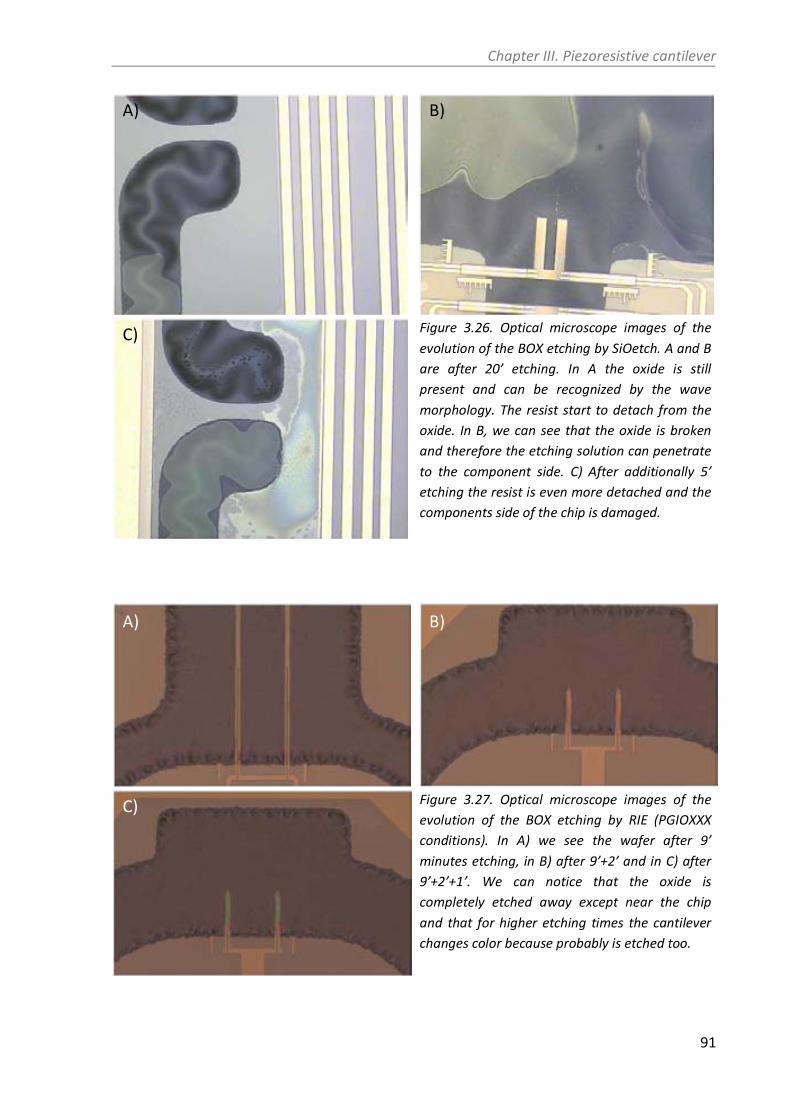
Chapter III. Piezoresistive cantilever
91
Figure 3.26. Optical microscope images of the
evolution of the BOX etching by SiOetch. A and B
are after 20’ etching. In A the oxide is still
present and can be recognized by the wave
morphology. The resist start to detach from the
oxide. In B, we can see that the oxide is broken
and therefore the etching solution can penetrate
to the component side. C) After additionally 5’
etching the resist is even more detached and the
components side of the chip is damaged.
Figure 3.27. Optical microscope images of the
evolution of the BOX etching by RIE (PGIOXXX
conditions). In A) we see the wafer after 9’
minutes etching, in B) after 9’+2’ and in C) after
9’+2’+1’. We can notice that the oxide is
completely etched away except near the chip
and that for higher etching times the cantilever
changes color because probably is etched too.
C)
B)A)
C)
B) A)

Force sensors based on piezoresistive and MOSFET cantilevers for biomolecular sensing
92
We had an improvement switching the conditions to PGIOXGUI, which have a selectivity
of 12:1. Even if we could perform longer etching times with lower risks to etch the silicon,
also in this case, after a total etching time of 14 minutes, we couldn’t etch completely the
oxide near the chip (Figure 3.28). In these pictures we can notice also that if there is still
oxide, the cantilevers are not in focus on the same plane of the chip because they are
deflected (Figure 3.28.A). The cantilevers are in focus on the same plane when the oxide is
etched (Figure 3.28.B). Since the oxide is transparent, it is quite challenging to detect its
presence through the resist by an optical microscope, therefore this fact can be used to
qualitatively evaluate the presence of the oxide underneath the cantilever. In SEM pictures
(Figure 3.28.C) we can see the final results. The oxide is etched away just in the cantilever
windows while around the chip is still present because the opening is two times narrower.
Finally, in Figure 3.28.D, we can notice that even if the oxide seems completely etched, on
the front part of the cantilever there is a kind of network. This is probably very thin silicon
oxide which folded on the cantilever. To eliminate this network longer etching time would
be needed with the risk to etch considerably also the silicon. In chapter 5, we will see that
even though this cantilevers can be used and have good sensitivity and noise performances,
they cannot be used to perform biomolecule force spectroscopy measurements.
As third option, we used HF vapors (RUN 4972). For this purpose we poured 100 ml of
49% HF into a 3.5’’ teflon beaker and we placed the wafer on the top. During these trials we
found three very important aspects. First: the etching speed of the HF vapors is affected a lot
by the atmosphere humidity [39]. In more humid days we saw that the etching was 2 times
faster than during less humid days. Second: recently deposited photoresist provide much
better barrier than “older” photoresist. The process should be performed just after the
silicon DRIE. In case that few weeks or months pass the resist detaches from the oxide much
faster. Third: the wafer should not be placed into water just after the vapor. When the wafer
is cleaned in DI water, we found that the resist and the component side had much worse
aspect than in the case that the wafer was left in air. This can be explained by the fact that
just after the process, absorbed HF is still present on the wafer surfaces and in contact with
water the HF-water solution penetrates faster and easier into the component side. Even if
we obtained very good results with this technique (wafer 4972-9), we didn’t manage to
obtain the same result in other wafers.

Chapter III. Piezoresistive cantilever
93
Figure 3.28. Optical and SEM microscope images
of the evolution of the BOX etching by RIE
(PGIOXGUI conditions). A) Wafer before etching
and B) wafer after 14 min. of etching: the
cantilevers are in focus on the same plane of the
chip. Some oxide is still present near the chip.
C,D) The oxide appears completely removed just
in the central part of the DRIE window. In the
close up we can appreciate that a very thin
silicon oxide network is folded on the cantilever.
E) Detail of a reference cantilever. The PECVD sil-
licon nitride covers pretty well the sidewalls of the cantilevers, providing therefore a good insulation
to the piezoresistor.
In this perspective it was important to have an equipment to have more repeatable HF
vapor etching. For this purpose we used an old custom made HF vapor etcher. After the first
trials we reported a very inhomogeneous etching speed across the wafer, which could vary
up to one order of magnitude. Therefore, as first, we modified the position of the holes of
the HF vapor “shower” to be as equidistant as possible one from each other. Then we used a
dummy silicon wafer to have a more homogenous temperature distribution across the wafer
that has to be etched (Figure 3.29). Additionally we inserted a 3 ways valve to choose a flow
of pure N2 or N2+HF+H2O vapors in order to condition the reaction chamber before and after
E)
D) C)
B) A)

Force sensors based on piezoresistive and MOSFET cantilevers for biomolecular sensing
94
the etching (Figure 3.30). Thanks to these three modifications we achieved relatively low
etching speed variations across the wafer (Figure 3.31). The first two valves that control the
N2 flow were turned for 360, for an approximate value of 2 l/min (the flow meter has a
maximum value of 1 l/min). If lower flow was chosen we found that the etching was less
homogeneous. Unfortunately we have not been able to vary the etching speed tuning the
temperature as reported in literature [40]. We had a kind of on-off etching behavior
dependent on the temperature (Figure 3.31). For values below 30 C we had etching speeds
(vetch) of 300 nm/min or higher. For temperatures higher than 33 C, we found almost no
etching (vetch<10 nm/min). At 32 C we had vetch180 nm/min but with big deviation. In the
literature the etching does not depend so strongly by the temperature. This strong
dependence can be explained by the fact that the thermocouple of the heater is not so
accurate. The temperature could be set with a 1 C of accuracy but during the use, the
temperature read on the display could vary ± 1 C. Considering these aspects I would
suggest to try using commercial HF vapor phase etcher from AMMT or Idonus or the more
complex etcher form Primaxx.
However we found that at 30 C we could have a relatively controlled etching speed of
300±50 nm/min (Figure 3.31). Before the etching we placed the wafer on the heating
substrate, we closed the reaction chamber and we let pass a N2 flow to condition the
chamber for 10 minutes. After the etching we conditioned the chamber for 10 minutes as
well to remove all the HF vapors.
Figure 3.29. Thermoreflectance images of the temperature distribution of the chuck surface of the HF
vapor etcher (A): the temperature can vary up to 5 C in the central area where the wafer is placed
during the etching. B) After placing a wafer, the temperature has better distribution and varies 0.5 C
as maximum. Just the temperature variation should be taken into consideration in these
measurement and not the absolute values.
B) A)

Chapter III. Piezoresistive cantilever
95
Figure 3.30. Schematics of the modified HF vapor etcher. The tubes with N2 flow are highlighted in
green. The tubes with N2+HF+ H20 flow are highlighted in red. Two valves control the N2 flow, while a
3-ways valve controls which gas enters in the reaction chamber. The gas is dispersed into the
chamber flowing through a “shower”. On the heater (orange), we place a dummy wafer to improve
the temperature homogeneity. On this, we place the process wafer. All the parts of the etcher are
made of teflon or HF resistant polymers.
24 26 28 30 32 34 360
100
200
300
400
etc
hin
g s
peed [nm
/min
]
Temperature [C]
Figure 3.31. Silicon oxide etching speed vs. heater temperature.
In Figure 3.32 and Figure 3.33 we report SEM pictures of the device in which the buried
oxide was etched by HF vapor.

Force sensors based on piezoresistive and MOSFET cantilevers for biomolecular sensing
96
Figure 3.32. Cantilevers after the BOX HF etching
(wafer 4972-9). (A) The cantilevers are lightly
bent upward. (B) Detail of the tip: the HF vapor
can leave very clean surfaces. (C) Detail of the
silicon nitride layer.
Figure 3.33. Cantilevers after the BOX HF etching
(wafer 6481-3) using the custom made etcher. A)
The BOX is not completely etched but the cantilevers
are released and bend upwards, probably because
some oxide is still present in the rear side of the
beams. B) Detail of the tip: the final part of the
cantilever is quite clean. C) Detail of the silicon
nitride layer. Even though it is slightly misaligned
due to the photolithography, it insulates well the
piezoresistor. The HF vapor partially etched the
silicon nitride which is not aligned on the cantilever.
C)
B) A)
C)
B) A)

Chapter III. Piezoresistive cantilever
97
Using the custom made etcher we could achieve quite satisfactory results (RUN 6481).
All the tested devices (25% of the total) were working and all the chips had no broken
cantilever, therefore we can consider a fabrication yield of 100%. Although other
researchers faced problems related with the BOX cracking during the release process that
led to the breaking of the cantilevers [41], we did not encounter similar problems. This is
probably due to the protective hard backed photoresist deposited on the component side.
Unfortunately, due to HF vapor release the insulating layer was partially etched from many
cantilevers. Considering the SEM images and the characterization in water (chapter 5) we
consider that at least 25% of the sensors function well in liquid environment. Improvements
in this direction can be achieved by using commercial HF etchers and changing the
component side protective layer. As reported [42], the photoresist has no good barrier
properties against HF vapors, but we used it for practical reasons. On the other hand
aluminum can be an option. From preliminary experiments we saw that a 500 nm thick Al-
layer offers a good barrier for the HF vapors (Figure 3.34) and can be used also to produce
very sharp silicon oxide tips. Of course the release of the cantilever from the aluminum layer
could lead to other problems like nitride etching, sticking, etc.
As we saw in the previous Figure 3.32 and Figure 3.33, the cantilever can be quite
horizontal or have strong bending. This difference can be seen comparing different wafers of
different RUNs but also comparing two chips across a single wafer. Considering this aspect, it
becomes quite challenging to reduce the curvature to desired values: for the same
fabrication process the layers can have different residual stresses in different wafers. The
bending, in part, can be due to residual oxide on the rear part of the beam and in part to the
variation of the layer thickness across the wafer. The layer thickness variation is not an issue
when relative thick cantilevers are fabricated, but can become a problem when we produce
nanomechanical structures. In this perspective, much job should be done in order to tune in
a repeatable way the residual stresses of the layers [6, 43]. For our purposes, the
functionality of the sensor is not compromised and as we will see in chapter 5 the cantilevers
function very well as biomolecule detectors and have very high resolution.
Figure 3.34. Cross section SEM images. The HF vapor etched approximately 850 nm of the exposed
thermal SiO2. The 500 nm thick Al- layer protected the oxide underneath. The etching has a typical
shape of an isotropic etching, as result tips with radius of 25 nm can be produced. The etching was
performed with the custom made etcher at 30 C for 2’30’’.
B) A)
silicon
oxide
aluminum

Force sensors based on piezoresistive and MOSFET cantilevers for biomolecular sensing
98
3.3 – Characterization
In this section we will present the different techniques that we used and developed to
measure the electrical, mechanical, electromechanical and noise characteristics of the
sensors to calculate their resolution. This part was of key importance for the success of the
project because if on one side it was very important a reliable fabrication process, on the
other side the validation of a technological process requires an intensive characterization of
the performances of the devices. Performing fast, accurate and repeatable mechanical,
electrical and electromechanical characterization of the device properties is necessary in
order to prove the reliability of the sensor and to validate the fabrication technology. For
these reasons, we decided to develop set ups that allows on-wafer properties
characterization, which results in a considerable reduction of the testing time respect to
previous set ups [44].
The most important parameters determining the performance of a quasi-static force
sensor based on piezoresistive cantilevers are the spring constant k [N/m], the force
sensitivity (SF,V) [V/N], the transducer noise [VNOISE] and the minimum detectable force (MDF)
[N].
3.3.1 – Mechanical
Due to the fact that that the cantilevers are very soft, it is not possible to measure
directly the spring constant, but it is calculated according to eq. (3.2). The thicknesses are
measured using an optical interferometer (Nanospec AFT 200 from Nanometrics). The
widths and lengths are verified using optical microscope and SEM images. The Young’s
modulus for silicon along <100> direction is taken as ESI= 130 GPa[45] and ESIO2= 75 GPa for
thermal oxide [46]. PECVD silicon nitride has been reported to present a wide range of
values for its Young’s modulus, instead, from 60 to 300 GPa [47-49] depending on the
deposition conditions and the layer thickness. Thus, it is necessary to experimentally
determine such value for our material. We performed micromechanical measurements with
a beam bending based technique [50] on stiffer (specifically designed) test cantilevers (see
section 3.2.1) using a commercial AFM (Bruker Dimension 3100). From these measurements
it is easy to calculate the spring constants of the test cantilevers. Then, it is possible to
extract the Young’s modulus of the silicon nitride layer using eqs. (2.47), (2.48), (2.52).
When the AFM probe is in contact with a cantilever, in the contact point we can write
the following equation to balance the forces (Figure 3.35.A):
(3.17)
where kC and C are the spring constant and deflection of the cantilever while kPeff and P are
the effective spring constant (kPeff=kP/cos2and =12º is the mounting angle of the probe)

Chapter III. Piezoresistive cantilever
99
and the deflection of the AFM probe. We know also that the total probe displacement (zP) is
the sum of the deflection of the probe and the one of the cantilever under test:
(3.18)
therefore we can write:
(3.19)
where tan is the slope of the deflection curve of the AFM probe while deflecting the
cantilever (Figure 3.35.B).
For these measurements we used an AFM probe with a measured spring constant KPeff=
(0.055 ±0.002) N/m (calibrated using Sader’s tune method [51]) in agreement with the
theoretical one (0.05 N/m). We initially performed multiple force curves on a single
cantilever to study the repeatability of the method from which we obtained a relative
standard deviation of 5%. This was then repeated on 9 cantilevers, to study the variation of
the spring constant in different points of the wafer. The mean value of the slope, for the
different cantilevers, is tan=0.306 (with a relative standard deviation of 6%) that indicates a
spring constant kC=(0.0240±0.0014) N/m and therefore an Enit=(70±7) Gpa. This value was
confirmed measuring the Young’s modulus of the 100 nm thick silicon nitride layer on silicon
oxide and aluminum substrate by the nanoindentantion technique performed via a XP MTS
Nano Indenter. With this value of the silicon nitride Young modulus, we calculated the spring
constant for the various cantilever designs (Table 3.4). Note that the rest of piezoresistive
cantilever designs have much lower spring constants and it was therefore not possible to
perform the spring constant calibration directly on them with this method. Finally, the value
of the spring constant of the cantilever design 2x250 has been also simulated in order to
verify the analytical model. The result agrees pretty well being just 1% higher.
0 100 200 300 400 500
0
100
200
300
C
cantilever
P
P [n
m]
zP[nm]
rigid surface
B)
Figure 3.35. A) Beam bending spring constant measurement: the AFM probe is deflecting the test
cantilever). The initial positions are shown in dashed lines. B) AFM probe deflection curves (P) against
the total AFM probe displacement (zP). In black the AFM probe is deflected against a stiff surface. This
curve is used to calibrate the AFM photodetector sensitivity. In red the AFM probe is deflected against
the cantilever under test: the difference between the two curves represent the deflection of the
cantilever under test (C).
A)

Force sensors based on piezoresistive and MOSFET cantilevers for biomolecular sensing
100
Cantilever
design
w1
[m]
w2
[m]
L1
[m]
L2
[m]
kC
[mN/m]
kC*
[mN/m]
(kC* -kC)/ kC
2x250 2 8 125 250 0.62±0.04 (0.617) 0.620 + 0.5%
6x250 6 16 125 250 1.73±0.11 - -
8x250 8 20 125 250 2.02±0.13 - -
Table 3.4. Spring constant for different cantilever designs. The spring constants are calculated from
eq. 3.5-3.7, considering the following Young’s moduli for silicon, silicon oxide and silicon nitride: 130
GPa, 75 GPa and 70 GPa. The standard deviation is calculated considering that the silicon nitride
modulus varies between 63 GPa and 77 GPa. kC* has been simulated by finite element method (using
Ansys), taking into consideration the same dimensions and young moduli.
3.3.2 – Electrical
The electrical characteristics of the piezoresistors are measured using a semiautomatic
probe station (PA200 from Karl Süss) and a semiconductor parameter analyzer (HP4155). I-V
curves are acquired for each piezoresistor by sweeping the bias voltage from -2.5 V to 2.5 V
in steps of 0.1 V while recording the current. We find a good ohmic contact between
aluminum and n-type silicon (Figure 3.36.A), very high fabrication yield (90%-100%) for the
best wafers (4972 wafers 4, 9, 10 and 6481 wafers 2, 3, 4, 5), and low relative standard
deviation of the resistance values for both the resistors implanted in the substrate and
embedded in the cantilevers (Table 3.5). In Figure 3.36.A, we reported the I-V graph for a
substrate resistor and a cantilever resistor from a chip of the wafer 6481-3. It is visible the
linear behavior of both resistors and that the cantilever resistor has higher resistivity. This
difference is in part explained by the different process that the two resistors have, as it will
be pointed out here afterwards (i.e. difference between the 2x250 and 2x250- designs). If
the results are plotted in R-V graph (Figure 3.36.B) we can notice that while the substrate
resistor is constant in this range, the cantilever has a U dependence. This is explained by the
fact that at higher voltages (positive or negative), the piezoresistor dissipate more power by
joule effect and as consequence the temperature of the cantilever increases and therefore
also the resistivity. For an increase of 500 at 2.5 V (with a power 300 W) and
considering a temperature coefficient of resistance between 500 and 1000 ppm/k [23], the
piezoresistor can have a maximum temperature increase of 125 C and 250 C. Even though
this seems a lot, we have to consider that since the cantilever has a very small volume it has
a very small heat capacity. This effect is not visible for substrate resistor since they are on
the chip which can be considered a heat sink.
In Table 3.5 we compare the resistance and the square resistances for three different
wafers (4972-4, 4972-9, 6481) that had different annealing times and temperature after the
OXPTAA annealing (75’ at 950 C in oxidizing atmosphere). The sheet resistances were

Chapter III. Piezoresistive cantilever
101
calculated considering that the total resistor length was 325 m, the width was 2 m and
that the contact resistance was negligible (less than 200 for each contact). As expected
from the model developed in the section 3.1, the sheet resistance decreases by increasing
the diffusion length.
From the wafer 6481-3 we can appreciate two main differences in three different
designs 2x250, 2x250+ and 2x250- (Table 3.6). First, for the design 2x250+ the substrate
resistance has a value 10% higher than the other two designs. In this design the annealing to
activate the doping atoms is done after removing the oxide deposited above the
implantation (i.e. in the same way that is done also for the cantilever piezoresistors). This is
probably due to a loss in arsenic that can derive in part from arsenic pile-up in the Si-SiO2
interface [52-54] and in part from exodiffusion [13]. According to the model and the
measurements, around 20% of the As atoms can be lost in wafers 6481-3 and 4972-4.
-3 -2 -1 0 1 2 3-150
-100
-50
0
50
100
150
I [
A]
VBIAS
[V]
cantilever
substrate
A)
-3 -2 -1 0 1 2 3
19
20
21
22
23
A)
cantilever
substrate
VBIAS
[V]
R [k
]
Figure 3.36. I-V (A) and R-V (B) graphs for a chip in the wafer 6481-3. The red corresponds to the
cantilever resistor and the black to the substrate resistor.
2x250 S
[k]
2x250 C
[k]
2x250 S
[]
2x250 C
[
n R tANN
[min]
TANN
[C]
6481-3 20.3±0.5 22.7±0.7 125±0.3 140±0.4 20 No No
4972-4 19.3±0.4 23.2±0.5 119±0.3 143±0.3 46 60 900
4972-9 16.3±0.3 18.2±0.7 100±0.2 112±0.4 46 30 1050
Table 3.5 Resistance and sheet resistance mean values ± standard deviation in 3 different wafers. The
values are divided between substrate resistor (S) and cantilever resistors (C). n R is the number of
measured resistors, tANN and TANN are the time and temperature of post oxidation annealing.
2x250 S
[k
2x250 C
[k
2x250 S
2x250 C
n R
2x250 20.3±0.5 22.7±0.7 125±0.3 140±0.4 20
2x250+ 22.0±0.4 23.0±0.5 135±0.3 142±0.3 20
2x250- 20.0±0.4 22.3±0.7 123±0.3 137±0.4 20
Table 3.6. Resistance and sheet resistance mean values ± standard deviation for 3 different designs in
wafer 6481-3. The statistic is made measuring 20 resistances for each design.
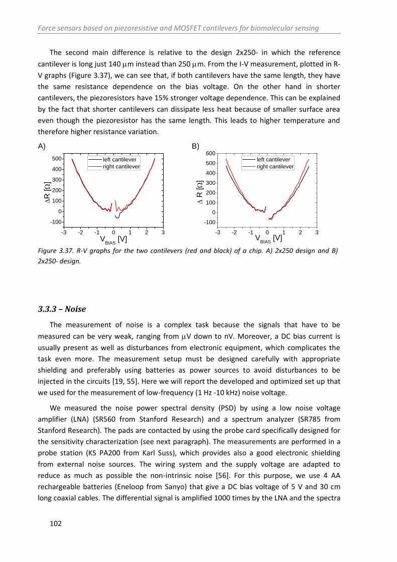
Force sensors based on piezoresistive and MOSFET cantilevers for biomolecular sensing
102
The second main difference is relative to the design 2x250- in which the reference
cantilever is long just 140 m instead than 250 m. From the I-V measurement, plotted in R-
V graphs (Figure 3.37), we can see that, if both cantilevers have the same length, they have
the same resistance dependence on the bias voltage. On the other hand in shorter
cantilevers, the piezoresistors have 15% stronger voltage dependence. This can be explained
by the fact that shorter cantilevers can dissipate less heat because of smaller surface area
even though the piezoresistor has the same length. This leads to higher temperature and
therefore higher resistance variation.
-3 -2 -1 0 1 2 3
-100
0
100
200
300
400
500
A)
R
[
]
VBIAS
[V]
left cantilever
right cantilever
-3 -2 -1 0 1 2 3
-100
0
100
200
300
400
500
600B)
R
[
]
VBIAS
[V]
left cantilever
right cantilever
Figure 3.37. R-V graphs for the two cantilevers (red and black) of a chip. A) 2x250 design and B)
2x250- design.
3.3.3 – Noise
The measurement of noise is a complex task because the signals that have to be
measured can be very weak, ranging from V down to nV. Moreover, a DC bias current is
usually present as well as disturbances from electronic equipment, which complicates the
task even more. The measurement setup must be designed carefully with appropriate
shielding and preferably using batteries as power sources to avoid disturbances to be
injected in the circuits [19, 55]. Here we will report the developed and optimized set up that
we used for the measurement of low-frequency (1 Hz -10 kHz) noise voltage.
We measured the noise power spectral density (PSD) by using a low noise voltage
amplifier (LNA) (SR560 from Stanford Research) and a spectrum analyzer (SR785 from
Stanford Research). The pads are contacted by using the probe card specifically designed for
the sensitivity characterization (see next paragraph). The measurements are performed in a
probe station (KS PA200 from Karl Suss), which provides also a good electronic shielding
from external noise sources. The wiring system and the supply voltage are adapted to
reduce as much as possible the non-intrinsic noise [56]. For this purpose, we use 4 AA
rechargeable batteries (Eneloop from Sanyo) that give a DC bias voltage of 5 V and 30 cm
long coaxial cables. The differential signal is amplified 1000 times by the LNA and the spectra

Chapter III. Piezoresistive cantilever
103
recorded by the spectrum analyzer (Figure 3.38). It is of key importance that the device
under test, the wirings and the LNA are placed inside the probe station to acquire a PSD free
as much as possible from non-intrinsic noise. Moreover, the LNA is operated in “battery”
mode which allows having lower amplifier noise. This set-up allows us also to have a single
ground (i.e. the ground of the signal analyzer) avoiding possible ground loops. In Table 3.7
we report the parameters for the LNA and the signal analyzer we used for all measurements.
The final PSD graph between 1Hz and 10 kHz (Figure 3.39) is the result of 4 different
bandwidth measurements: 0.125-12.5 Hz, 0.5-200 Hz, 2-1600 Hz and 16-12800 Hz. Each
bandwidth had different number of fast Fourier transform (FFT) lines and therefore different
binwidth: 0.125 Hz, 0.5 Hz, 2 Hz and 16 Hz respectively. Each PSD was the average of 50
curves. Finally, we unfortunately noticed that during the weekends the measurements were
more stable, repeatable and there were less external interferences. This is due to the fact
that almost all the equipments in the IMB-CNM are shut down, which provokes to have less
interference. In this perspective, the quasi totality of the noise measurements has been
performed during non-working hours.
SR560 SRS785
Coupling AC Coupling AC
Inputs A-B Input A
filters 0.03-300K Window Hanning
Gain 1000 Span [Hz] 12.5 200 1600 12800
Input 100 M, 25pF FFT lines 100 400 800 800
Output 50 Binwidth
[Hz] 0.125 0.5 2 16
Table 3.7. Parameters of the low noise voltage amplifier (SR560) and the dynamic analyzer
(SRS785) for the noise measurements.
Figure 3.38. Noise and sensitivity measurements electrical scheme. The differential voltage of the
Wheatstone bridge is amplified by the low noise voltage amplifier. The noise spectrum is recorded by
the signal analyzer while the sensitivity signal is recorded by the AFM electronics (see next section).

Force sensors based on piezoresistive and MOSFET cantilevers for biomolecular sensing
104
After the optimization of the set up, we tested the repeatability of the measurement,
recording the noise spectrum 9 times for a single chip taking on and off the set up each time.
We obtained a relative standard deviation of 2% for the integrated noise in the 1 Hz-10 kHz
bandwidth. Then we measured the noise spectra of all the chips across the wafer for one
wafer (4972-9) and of fewer chips for two other wafers (4972-4 and 6481). In Figure 3.39, we
report typical input referred noise power spectral density for the three different wafers. In
Table 3.8, we report the mean voltage noise value referred to input (Vnoise) measured
between 1Hz and 10 kHz and the Hooge factor.
As we can see from the graphs and the average voltages there are substantial differences
between the wafers 4972 and 6481. Although in the literature it is reported that for thermal
treatments with higher diffusion length the 1/f noise and Hooge factor decrease, we found
the opposite behavior. While substantially agree with literature values for wafer 6481 [23],
it is much higher for wafers 4972. This can be explained by the fact that the aluminum RIE
damaged the crystalline structure of the implanted silicon in wafer 4972 because longer
over-etching has been used. On the other hand in wafer 6481, we reduced as much as
possible the etching time and the aluminum residues have been etched by wet etching.
Extreme care should be taken for the back end of line process, after the piezoresistor is
formed. Reactive ion etching should be avoided whenever possible and they should be
replaced by wet etching or better by lift-off processes.
A second important point is that a good nitride passivation, which insulates the
piezoresistor in liquid environment, is of fundamental importance for both air and water
environments. The noise spectral density of a device (wafer 6481-3) immersed in water,
shown in Figure 3.39.E, shows that the silicon nitride layer provides a good insulation for the
conductors immersed in liquid. On the other hand, in Figure 3.40.A, we can see the noise
spectra of a chip (4972-4) measured just after biasing and after few minutes. The low
frequency noise spectra increases of around 1 order of magnitude and loose the typical 1/f
noise shape. This is probably due to the fact that in wafer 4 the nitride passivation layer has
been damaged during the HF vapor release (Figure 3.40.B).
Finally, for the sensors of the wafer 6481-4, the noise spectra have a 1/fn behavior
between 1 Hz and 10 Hz (Figure 3.39.C). This has been reported already by other researchers
[11] and it has been explained by “temperature fluctuations or thermomechanical coupling
due to unstable convection around the cantilever, leading to temperature fluctuations which
are electrically coupled via a change in piezoresistivity with temperature”

Chapter III. Piezoresistive cantilever
105
100
101
102
103
104
10-16
10-15
10-14
10-13
10-12
10-11
A)
Frequency [Hz]
PS
D [V
2 RM
S/H
z]
100
101
102
103
104
10-16
10-15
10-14
10-13
10-12
10-11
B)
PS
D [V
2 RM
S/H
z]
Frequency [Hz]
100
101
102
103
104
10-16
10-15
10-14
10-13
10-12
10-11
C)
PS
D [V
2 RM
S/H
z]
Frequency [Hz] 10
010
110
210
310
410
-16
10-15
10-14
10-13
10-12
10-11
D)
OXPTAA + 1050ºC-30'
OXPTAA + 900ºC-60'
OXPTAA
PS
D [V
2 RM
S/H
z]
Frequency [Hz]
100
101
102
103
104
10-16
10-15
10-14
10-13
10-12
10-11
air
water
PS
D [V
2 RM
S/H
z]
Frequency [Hz]
E)
Figure 3.39. Typical input referred noise power spectral
density for the Wheatstone bridge of three different chips
with design 2x250 in wafer 4972-9 (= 1.3x10⁻³) (A),
4972-4 (= 7.4x10⁻⁴) (B) and 6481-3 (= 3x10⁻⁴) (C). The
linear fittings of the 1/f and thermal noise are reported in
red. The bridges are biased by a constant voltage of 5 V
and the pads are contacted by the probe card. In D) it is
reported the overlapping of the three PSD. E) Overlapping
of the noise for the same chip measured in air and water.
Considering the 1 Hz-10 kHz bandwidth we calculate a
noise of 3.7 V in air (black) and 3.8 uV in water (blue)
WAFER DESIGN
[nm]
Vnoise
[V]
(x10-3)
n sensors
4972-9 2x250 95 6.7±1.0 1.3±0.2 24
4972-9 6x250 95 5.5±0.6 2.8±0.3 24
4972-9 8x250 95 6.9±0.7 1.4±0.1 24
6481-4 2x250 42 3.9±0.8 0.3±0.1 10
Table 3.8. Diffusion length( ), input referred noise integrated in the 1 Hz - 10 kHz bandwidth
(Vnoise), Hooge factor (), for different cantilever designs and in different wafers. The statistics are
made out of 24 or 10 sensors across the wafer.

Force sensors based on piezoresistive and MOSFET cantilevers for biomolecular sensing
106
101 102 103 10410-17
10-16
10-15
10-14
10-13
A)A)
PS
D [V
2 RM
S/H
z]
Frequency [Hz]
Figure 3.40. A) Input referred noise power spectral density for the Wheatstone bridge of the majority of
the chips from the wafer 4972-4. In black the PSD when the chip is just biased; in red the PSD when the
chip is biased for 10 minutes. B) SEM image of the cantilever: it is visible how the silicon nitride
passivating layer is damaged.
3.3.4 – Sensitivity and resolution
The displacement sensitivity, S,V=V/, can be measured by performing an accurate
deflection of the cantilever while recording the resistance variation or, in our case, the
voltage variation of the Wheatstone bridge. In order to deflect the cantilever with high
accuracy, various approaches have been used, such as a needle mounted on a bimorph
piezodisk [57], a calibrated piezotube [58], an AFM in contact mode [59] or in tapping mode
[60], etc. A parallel approach, only valid for very low stiffness devices, measures the
resonant thermomechanically-driven displacement fluctuations [21, 59]. All these methods
allowed a precise estimation of the device deflection sensitivity but were carried out on a
chip level, therefore making technology validation a tedious and long process. An
alternative, which allows for on-wafer testing, is to deflect the cantilever by a needle
mounted on a micromanipulator [61]. However, this method is far less accurate than the
previously mentioned solutions.
Here, we present a novel set-up and technique that allows on-wafer characterization
with high accuracy, good repeatability and unprecedented reduction in testing time. For this
purpose, we designed a special probe-card (Figure 3.41.A), which was fabricated by
HTT.GmbH in Dresden (Figure 3.41.B). It allowed us to contact the pads of a chip and
simultaneously deflect them by other means. In particular, its reduced size permitted the
use of an AFM (Dimension 3100 or Dimension Icon of Bruker) to deflect the cantilevers, thus
benefiting from the high motional precision of such equipment. The probe-card presented
here was specifically designed to be used in the Dimension 3100 AFM, could access all the
devices across the 4’’ wafer, using a micropositioner (500 MIS from Quater). The probes had
to be long and almost horizontal in order to avoid any interaction with the head and probe
B)

Chapter III. Piezoresistive cantilever
107
holder of the AFM (Figure 3.41.C) and were correctly aligned onto the chip pads using the
optical microscope of the AFM. In addition, the PCB had to be small to fit onto the AFM
chuck. The two grooves (visible in the left part of the top view) increased the travel range of
the micropositioner. To bias the chips, we used a voltage source (2636 from Keithley) or 4
AA rechargeable batteries (Eneloop from Sanyo) in series, which provided a constant voltage
of 5 V. A low noise voltage amplifier (SR 560 from Stanford Research) was used to amplify
the differential output signal (Figure 3.38). In Figure 3.42 and Figure 3.43, it is possible to see
the complete set up. The wafer was placed on the chuck of the AFM and the probecard was
moved on a chip to contact the pads. Then, a stiff AFM probe (k≈40 N/m) was used to
deflect the cantilevers at a certain distance from the clamping edge (namely at 140±3 m or
at the free end). The output differential voltage was amplified and recorded continuously
together with the AFM probe displacement (Figure 3.44).
Figure 3.41. A) Lateral view (up) and top view (down) of the probe card design (dimensions in mm).
For the probes we fixed the maximum vertical drop to 0.7 mm and the length to 16 mm to avoid any
interaction with the AFM head. B) Probecard fabricated by HTT.GmbH in Dresden. C) The probes have
to contact the pads of the chips without interacting with the AFM probeholder or with the AFM head
while the AFM probe is in contact (dimensions in mm).
C)
B) A)
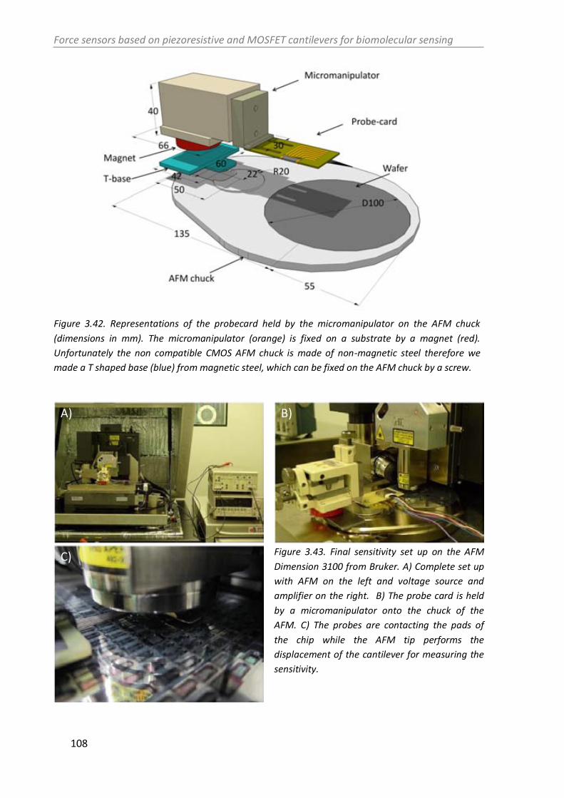
Force sensors based on piezoresistive and MOSFET cantilevers for biomolecular sensing
108
Figure 3.42. Representations of the probecard held by the micromanipulator on the AFM chuck
(dimensions in mm). The micromanipulator (orange) is fixed on a substrate by a magnet (red).
Unfortunately the non compatible CMOS AFM chuck is made of non-magnetic steel therefore we
made a T shaped base (blue) from magnetic steel, which can be fixed on the AFM chuck by a screw.
Figure 3.43. Final sensitivity set up on the AFM
Dimension 3100 from Bruker. A) Complete set up
with AFM on the left and voltage source and
amplifier on the right. B) The probe card is held
by a micromanipulator onto the chuck of the
AFM. C) The probes are contacting the pads of
the chip while the AFM tip performs the
displacement of the cantilever for measuring the
sensitivity.
C)
B) A)

Chapter III. Piezoresistive cantilever
109
In order to precisely position the AFM tip on top of the device and work under low
interaction forces, the AFM was operated in dynamic mode. In this mode, the tip-sample
interaction is controlled by maintaining fixed amplitude of AFM probe oscillating at its
resonance frequency. This gave us another advantage and was the ability to detect when the
AFM probe contacts the piezoresistive cantilever, which was when the oscillation amplitude
dropped to zero. Since the stiffness of the AFM probe was much bigger than the one of the
cantilever under investigation (4 or 5 orders of magnitude), its static deflection was
negligible. After one measurement that typically was performed at 1 Hz, the probe card
could be moved to the next chip by using the micromanipulator. The AFM allowed a precise
positioning of the probe along the cantilever thanks to the optical microscope and to the
motorized positioning stage which has a repeatability of ± 3 m. We had also very good
control of the deflection, due to the piezoactuator of the AFM.
Figure 3.44 shows a typical deflection experiment. From these measurements, we
obtained the displacement sensitivity (S=V/) and we calculated the gauge factor (G) or
piezoresistive coefficient (11) and the force sensitivity (SF,V=V/F) for a force F applied in the
end of the cantilever (3.8).
In Figure 3.45, we report the difference deflection sensitivity for the same cantilever
deflected at 140 m and 250m far from the clamping edge. In the first case, the force
sensitivity at the tip was calculated from the sensitivity model (3.8). If the cantilever was
deflected at the tip, then the force sensitivity was calculated considering the nominal spring
constant. In this example we can appreciate that the two calculated values (180v/nN and
170 v/nN) are in a good agreement.
In order to check the repeatability of the measurement method, we performed multiple
force curves on the same piezoresistive cantilever with the AFM probe being always in
contact and we obtained a relative standard deviation of less than 2% out of 8
measurements (Figure 3.46.A). This variability is mainly due to low frequency noise and to
the linear fitting. In addition, we performed repeatability experiments also taking on and off
the set up each time performing the force distance curve on the same cantilever at the same
point. As expected, we obtained a higher relative standard deviation of around 3% out of 5
measurements (Figure 3.46.B). The higher variability should be addressed to the uncertainty
of the positioning system. The variation agrees with the electromechanical model developed
in section 3.1.
In addition to the repeatability, we studied also the variation of the sensitivity of the
chips across the wafers (Figure 3.47). In Table 3.9 we report the mean value of the
sensitivities, noise and MDF. This shows that our measurement system is particularly suited
to technology characterization where several device types and several device geometries
within a type have to be measured.

Force sensors based on piezoresistive and MOSFET cantilevers for biomolecular sensing
110
0.0 0.5 1.0 1.5
0
10
20
30
40
p
rob
e v
ibra
tio
n a
mp
litu
de
[n
m]
probe z-displacement [m]
diffe
ren
tia
l o
utp
ut vo
lta
ge
[m
V]
-0.15
-0.10
-0.05
0.00
0.05
0.10
0.15
0.20
0.25
approach
retra
ct
Figure 3.44. Electromechanical response of a piezoresistive cantilever (8x250). At a length of 140 m,
a stiff probe (in tapping mode) starts to deflect downwards the cantilever when the vibration
decreases from around 40 nm to almost 0 nm. At the same time the output differential voltage of the
Wheatstone bridge (WB) starts to increase (blue line) from 14.03 mV to 14.24 mV for a deflection of
0.91 m. This means a displacement sensitivity of around 231 µV/um at the deflection point and a
force sensitivity of 46 µV/nN at the tip. In the retract curve (red) is also visible the strong interaction
between the AFM tip and the cantilever under test which is bending upwards for 0.5 m. The force
curve (approach and retract) is performed over 1 second.
0.0 0.5 1.0 1.50
10
20
30
40
p
rob
e v
ibra
tio
n a
mp
litu
de
[n
m]
probe z-displacement [m]
diffe
ren
tia
l o
utp
ut vo
lta
ge
[m
V]
7.6
7.7
7.8
7.9
8.0
8.1
140 m
250 m
5.5
5.6
5.7
5.8
5.9
6.0
Figure 3.45. Sensitivity measurements on a piezoresistive cantilever (2x250). The AFM probe
performs a force curve on the test cantilever at 140 m from the clamping edge or at 250 m (i.e. at
the cantilever end). In the first case, the output voltage goes from 7.65 mV to 8.04 mV. This
correspond to a displacement sensitivity of 261 V/m and to a force sensitivity at the tip of 180
V/nN. In the second case the voltage varies between 5.67 mV and 5.83 mV, which means a
displacement sensitivity of 106 V/m and a force sensitivity at the tip of 170 V/nN in agreement
with the previous measurement. The vibration amplitude of the AFM probe is stable at 0 nm for all
the measurement (i.e. the probe is always in contact).
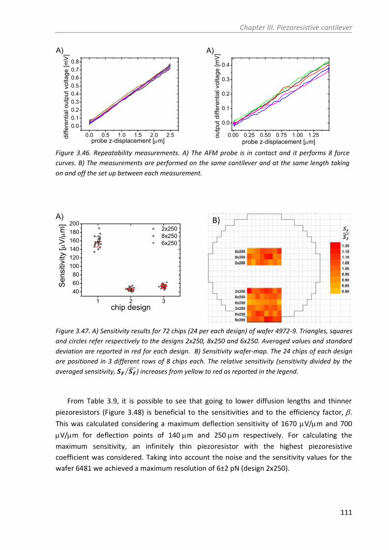
Chapter III. Piezoresistive cantilever
111
0.0 0.5 1.0 1.5 2.0 2.50.00.10.20.30.40.50.60.70.8
probe z-displacement [m]diffe
rent
ial o
utpu
t vol
tage
[mV
] A)
0.00 0.25 0.50 0.75 1.00 1.25
0.0
0.1
0.2
0.3
0.4
A)
outp
ut d
iffer
entia
l vol
tage
[mV
]
probe z-displacement [m] Figure 3.46. Repeatability measurements. A) The AFM probe is in contact and it performs 8 force
curves. B) The measurements are performed on the same cantilever and at the same length taking
on and off the set up between each measurement.
1 2 3406080
100120140160180200
A) 2x250 8x250 6x250
Sens
itivi
ty [
V/m
]
chip design
Figure 3.47. A) Sensitivity results for 72 chips (24 per each design) of wafer 4972-9. Triangles, squares
and circles refer respectively to the designs 2x250, 8x250 and 6x250. Averaged values and standard
deviation are reported in red for each design. B) Sensitivity wafer-map. The 24 chips of each design
are positioned in 3 different rows of 8 chips each. The relative sensitivity (sensitivity divided by the
averaged sensitivity, ) increases from yellow to red as reported in the legend.
From Table 3.9, it is possible to see that going to lower diffusion lengths and thinner
piezoresistors (Figure 3.48) is beneficial to the sensitivities and to the efficiency factor,.
This was calculated considering a maximum deflection sensitivity of 1670 V/m and 700
V/m for deflection points of 140m and 250m respectively. For calculating the
maximum sensitivity, an infinitely thin piezoresistor with the highest piezoresistive
coefficient was considered. Taking into account the noise and the sensitivity values for the
wafer 6481 we achieved a maximum resolution of 6±2 pN (design 2x250).
B)

Force sensors based on piezoresistive and MOSFET cantilevers for biomolecular sensing
112
Wafer Design S
Deflection
Point
tR
SF,V
11
x10-11
n⁰
chips
Noise 1Hz-
10kHz
MDF
[V/m] [m] [nm] [V/nN] [Pa-1] [V] [pN]
4972-
4
2x250 510±28 140 115 0.31 320±18 61±3 23 21
8x250 470±40 140 115 0.28 100±9 56±5 23 69
6x250 510±25 140 115 0.31 120±6 62±3 20 46
4972-
9
2x250 240±19 140 185 0.14 160±13 67±5 24 6.7±1.0 42±9
8x250 230±20 140 185 0.14 40±3 64±6 24 6.9±0.7 170±30
6x250 230±18 140 185 0.14 50±4 64±5 24 5.5±0.6 110±19
6481 2x250 400±50 250 70 0.57 650±75 88±10 10 3.9±0.8 6±2
Table 3.9. Deflection sensitivity (S), deflection point from the clamping edge, piezoresistor thickness
(tR) from TOF-SIMS measurements (Figure 3.48), efficiency factor, force sensitivity (SF,V), piezoresistive
coefficient, number of measured chips, input referred noise in the 1Hz 10 kHz bandwidth, force
resolution (MDF). The force resolution of the three designs of the wafer 4972-4 it has been calculated
considering the noise of the designs of the wafer 4972-9.
0 100 200 300 400 500
0.01
0.1
1 OXPTAA
OXPTAA + 900ºC-60'
OXPTAA + 1050ºC-30'
rela
tive
co
un
ts
depth [nm]
Figure 3.48. TOF-SISM measurements of the implantation for the three different wafers. For higher
diffusion length the junction has also higher depth. The real profiles have been approximated with
step profile functions (continuous line) to calculate the average piezoresistive coefficient in Table 3.9.
The depths of the step profiles are calculated supposing that all the atoms are within this profiles
which have a constant concentration.
In Table 3.10, the sensitivity calculated from the model is compared to the measured
sensitivity, for the three different wafers. The results agree quite well for the first two wafers
while for the wafer 6481 the experimental sensitivity is almost two times higher respect to
the predicted one. This can be due to many factors related to the model and to the

Chapter III. Piezoresistive cantilever
113
measured devices, as for example: sub-estimation of the piezoresistive coefficient in the
model, initial bending of the cantilever, BOX not completely etched. Considering the
deviation, an upgrade of the model that takes into account the real dopant profile, could be
beneficial also for an improvement of the sensor performance. This would require also
process simulations [18] and piezoresistance experiments [30].
Concluding, the use of the probe-card together with a manual micromanipulator allowed
characterizing a considerable number of chips in a relatively short time (20-30 chip/hour for
expert users) across the whole wafer. This constitutes a definite improvement with the way
these measurements were done up to date [60], where the chip had to be pulled apart from
the wafer, attached on a PCB board and wire bonded, which is a time consuming, risky and
not robust process. In addition, with the new method we reduced also the risk to damage
the sensor. An additional way to decrease the measurement time would be to automate in
part the measurement set up using a motorized micromanipulator. However, there is a limit
to the amount of the automation due to the complex nature of the electro-mechanical
measurement. Finally from the sensor point of view, we achieved our target to fabricate, in a
reliable way, sensors endowed with sub-10 pN resolution suitable to be used in biomolecule
detection.
Wafer Design SF,V
[V/nN]
SF,V*
[V/nN]
4972-4 2x250 320 282 +13%
4972-9 2x250 160 128 +25%
6481 2x250 650 342 +91%
Table 3.10. Measured force sensitivity (SF,V), calculated sensitivity (SF,V*), relative difference between
model and experimental values.

Force sensors based on piezoresistive and MOSFET cantilevers for biomolecular sensing
114

Chapter III. Piezoresistive cantilever
115
Summary and future research directions
The main objective of the work presented in this chapter was to obtain a high number of
force sensors based on piezoresistive cantilevers, enabled with a resolution of around 10 pN
in liquid environment, to be used in the detection of intermolecular forces. Such a high force
resolution was needed in view of the very low unbinding forces of single pairs of receptor
and ligand molecules, which are in the order of 10 - 100 pN.
In the first section, the electromechanical model to evaluate the resolution of the sensor
has been presented. This was used to find the right parameter values to improve the
performance of the cantilevers which were previously developed at CNM and had a
resolution of 65 pN, which was not sufficient for our purposes.
Afterwards, it has been presented the microfabrication process that allowed a
fabrication yield between 90% and 100%, in the best wafers. The main fabrication issues
have been also addressed (i.e. metal and buried oxide etchings). Different fabrication
solutions have been taken to improve especially the sensitivity and the noise. Thanks to the
optimization of two key process steps (i.e. relatively low annealing temperature, a
combination of dry and wet metal etching), we obtained sensors with a sensitivity of 650±75
V/nm, a noise of 3.8±0.8 V and a resolution of 6±2 pN. A big improvement in the yield was
then represented by the upgrading of a custom made HF vapor etcher. Thanks to it, we
could etch the buried oxide more homogeneously and in a more reliable way. This translated
to lower risk to damage the silicon nitride insulation layer and to higher number of well
passivated sensors (between 25% and 50% of all the chips in a wafer).
A third, very important, aspect to achieve the objective, was the development of highly
precise and high-throughput electro-mechanical characterization techniques and set-ups to
correctly validate the technological processes involved in production as well to characterize
all the final devices. In particular, the integration of a probe-card into an AFM allowed a fast
and precise on-wafer sensitivity measurement and the use of a preamplifier and a spectrum
analyzer with a probe-station allowed a reliable on-wafer noise characterization. The
complete characterization of an entire wafer became possible in a reasonable time (≈1
week). Mechanical, electrical, noise and electromechanical average properties have been
reported for 3 different wafers.
In different points of the chapter, several advices to improve the performance and the
yield of the sensor have been point out:
Improvement of piezoresistive and noise properties of doped silicon in structures
those are much easier to fabricate than cantilevers.
Fabrication of the chip metal interconnections by lift-off process instead than
sputtering and etching. To this purpose a reversible resist with a thickness between 3
m and 5 m with a pronounced undercut could work pretty well (i.e. TI 35ES from
MicroChemicals GmbH)

Force sensors based on piezoresistive and MOSFET cantilevers for biomolecular sensing
116
Upgrade further the HF vapor etcher or better use a commercial one to etch in a
more uniform way the BOX. Commercially available equipment exists from AMMT
GmbH, Idonus or SPTS Primaxx.

Chapter III. Piezoresistive cantilever
117
References
1. Petersen, K.E., Silicon as a mechanical material. Proceedings of the IEEE, 1982. 70(5): p.
420-457. 2. Hopcroft, M.A., W.D. Nix, and T.W. Kenny, What is the Young's Modulus of Silicon?
Journal of Microelectromechanical Systems. 19(2): p. 229-238. 3. Yota, J., Effects of Deposition Method of PECVD Silicon Nitride as MIM Capacitor
Dielectric for GaAs HBT Technology. ECS Transactions, 2011. 35(4): p. 229-240. 4. Osenbach, J.W., Corrosion-induced degradation of microelectronic devices.
Semiconductor science and technology, 1996. 11(2): p. 155. 5. Lin, H., et al., Moisture-resistant properties of SiNx films prepared by PECVD. Thin Solid
Films, 1998. 333(1-2): p. 71-76. 6. Wei, J., et al., A new fabrication method of low stress PECVD SiNx layers for biomedical
applications. Thin Solid Films, 2008. 516(16): p. 5181-5188. 7. Tortonese, M., R.C. Barrett, and C.F. Quate, Atomic resolution with an atomic force
microscope using piezoresistive detection. Applied Physics Letters, 1993. 62(8): p. 834-836.
8. Harjee, N., Coaxial-tip Piezoresistive Cantilever Probes for High-resolution Scanning Gate Microscopy2011: Stanford University.
9. Thaysen, J., et al., Atomic force microscopy probe with piezoresistive read-out and a highly symmetrical Wheatstone bridge arrangement. Sensors and Actuators A: Physical, 2000. 83(1-3): p. 47-53.
10. Park, S.-J., J.C. Doll, and B.L. Pruitt, Piezoresistive Cantilever Performance-Part I: Analytical Model for Sensitivity. Journal of Microelectromechanical Systems, 2010. 19(1): p. 137-148.
11. Park, S.-J., et al., Piezoresistive Cantilever Performance-Part II: Optimization. Journal of Microelectromechanical Systems, 2010. 19(1): p. 149-161.
12. Jones, S.W., Diffusion in Silicon, 2008: ICKnowledge LLC. 13. Guia, G.B., recuita termica rapida de silici implantat amb arsenic per a la fabricacio
d'unions poc profundes, 1989, Universidad Autonoma de Barcelona. 14. Tsai, M.Y., et al., Shallow junctions by high-dose As implants in Si: experiments and
modeling. Journal of Applied Physics, 1980. 51(6): p. 3230-3235. 15. Liu, T.M. and W.G. Oldham, Sheet resistance-junction depth relationships in implanted
arsenic diffusion. Electron Device Letters, IEEE, 1981. 2(10): p. 275-277. 16. Harley, J.A. and T.W. Kenny, 1/f noise considerations for the design and process
optimization of piezoresistive cantilevers. Microelectromechanical Systems, Journal of, 2000. 9(2): p. 226-235.
17. Doll, J.C., et al. High frequency force sensing with piezoresistive cantilevers. in Solid-State Sensors, Actuators and Microsystems Conference, 2009. Transducers 2009. International. 2009.
18. Doll, J.C., Advances in high bandwidth nanomechanical force sensors with integrated actuation, 2012, Stanford University.
19. Dieme, R., Investigation of process fabrication for low-noise p-type diffused piezoresistors 2009, University of Florida.
20. Zeghbroeck, B.V., Principles of semiconductor devices2011: online book at http://ecee.colorado.edu/~bart/book/.
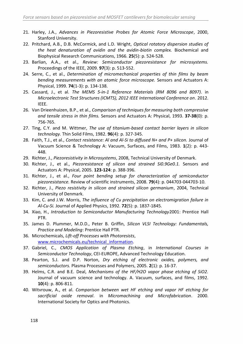
Force sensors based on piezoresistive and MOSFET cantilevers for biomolecular sensing
118
21. Harley, J.A., Advances in Piezoresistive Probes for Atomic Force Microscope, 2000, Stanford University.
22. Pritchard, A.B., D.B. McCormick, and L.D. Wright, Optical rotatory dispersion studies of the heat denaturation of avidin and the avidin-biotin complex. Biochemical and Biophysical Research Communications, 1966. 25(5): p. 524-528.
23. Barlian, A.A., et al., Review: Semiconductor piezoresistance for microsystems. Proceedings of the IEEE, 2009. 97(3): p. 513-552.
24. Serre, C., et al., Determination of micromechanical properties of thin films by beam bending measurements with an atomic force microscope. Sensors and Actuators A: Physical, 1999. 74(1-3): p. 134-138.
25. Cassard, J., et al. The MEMS 5-in-1 Reference Materials (RM 8096 and 8097). in Microelectronic Test Structures (ICMTS), 2012 IEEE International Conference on. 2012. IEEE.
26. Van Drieenhuizen, B.P., et al., Comparison of techniques for measuring both compressive and tensile stress in thin films. Sensors and Actuators A: Physical, 1993. 37-38(0): p. 756-765.
27. Ting, C.Y. and M. Wittmer, The use of titanium-based contact barrier layers in silicon technology. Thin Solid Films, 1982. 96(4): p. 327-345.
28. Faith, T.J., et al., Contact resistance: Al and Al-Si to diffused N+ and P+ silicon. Journal of Vacuum Science & Technology A: Vacuum, Surfaces, and Films, 1983. 1(2): p. 443-448.
29. Richter, J., Piezoresistivity in Microsystems, 2008, Technical University of Denmark. 30. Richter, J., et al., Piezoresistance of silicon and strained Si0.9Ge0.1. Sensors and
Actuators A: Physical, 2005. 123-124: p. 388-396. 31. Richter, J., et al., Four point bending setup for characterization of semiconductor
piezoresistance. Review of scientific instruments, 2008. 79(4): p. 044703-044703-10. 32. Richter, J., Piezo resistivity in silicon and strained silicon germanium, 2004, Technical
University of Denmark. 33. Kim, C. and J.W. Morris, The influence of Cu precipitation on electromigration failure in
Al-Cu-Si. Journal of Applied Physics, 1992. 72(5): p. 1837-1845. 34. Xiao, H., Introduction to Semiconductor Manufacturing Technology2001: Prentice Hall
PTR. 35. James D. Plummer, M.D.D., Peter B. Griffin, Silicon VLSI Technology: Fundamentals,
Practice and Modeling: Prentice Hall PTR. 36. Microchemicals, Lift-off Processes with Photoresists,
www.microchemicals.eu/technical_information. 37. Gabriel, C., CMOS Application of Plasma Etching, in International Courses in
Semiconductor Technology, CEI-EUROPE, Advanced Technology Education. 38. Pearton, S.J. and D.P. Norton, Dry etching of electronic oxides, polymers, and
semiconductors. Plasma Processes and Polymers, 2005. 2(1): p. 16-37. 39. Helms, C.R. and B.E. Deal, Mechanisms of the HF/H2O vapor phase etching of SiO2.
Journal of vacuum science and technology. A. Vacuum, surfaces, and films, 1992. 10(4): p. 806-811.
40. Witvrouw, A., et al. Comparison between wet HF etching and vapor HF etching for sacrificial oxide removal. in Micromachining and Microfabrication. 2000. International Society for Optics and Photonics.

Chapter III. Piezoresistive cantilever
119
41. Hill, G.C., et al., Patterned cracks improve yield in the release of compliant microdevices from silicon-on-insulator wafers. Journal of Micromechanics and Microengineering, 2011. 21(8): p. 087001.
42. Bakke, T., et al. Etch stop materials for release by vapor HF etching. in 16 MicroMechanics Europe Workshop (MME) 2005. Göteborg, Sweden.
43. Fang, W. and J.A. Wickert, Determining mean and gradient residual stresses in thin films using micromachined cantilevers. Journal of Micromechanics and Microengineering, 1996. 6(3): p. 301-309.
44. Villanueva, L.G., Development of Cantilevers for Biomolecular Measurements, 2006, Universitat Autonoma de Barcelona.
45. Wortman, J.J. and R.A. Evans, Young's Modulus, Shear Modulus, and Poisson's Ratio in Silicon and Germanium. Journal of Applied Physics, 1965. 36(1): p. 153-156.
46. Halg, B. On a nonvolatile memory cell based on micro-electro-mechanics. in Micro Electro Mechanical Systems, 1990. Proceedings, An Investigation of Micro Structures, Sensors, Actuators, Machines and Robots. IEEE. 1990.
47. Gavan, K.B., et al., Size-dependent effective Young's modulus of silicon nitride cantilevers. Applied Physics Letters, 2009. 94(23).
48. Huang, H., et al., Effect of deposition conditions on mechanical properties of low-temperature PECVD silicon nitride films. Materials Science and Engineering: A, 2006. 435-436: p. 453-459.
49. McShane, G.J., et al., Young's modulus measurement of thin-film materials using micro-cantilevers. Journal of Micromechanics and Microengineering, 2006. 16(10): p. 1926-1934.
50. Langlois, E.D., et al., Spring constant calibration of atomic force microscopy cantilevers with a piezosensor transfer standard. Review of Scientific Instruments, 2007. 78(9).
51. Sader, J.E., Frequency response of cantilever beams immersed in viscous fluids with applications to the atomic force microscope. Journal of Applied Physics, 1998. 84(1): p. 64-76.
52. Shibahara, K., et al. Dopant loss origins of low energy implanted arsenic and antimony for ultra shallow junction formation. in Material Research Society Symposium Proceedings. 1998. Materials Research Society.
53. Rubio, J.E., et al., Dose loss and segregation of boron and arsenic at the Si/SiO2 interface by atomistic kinetic Monte Carlo simulations. Materials Science and Engineering: B, 2005. 124: p. 392-396.
54. Koh, M., et al., Quantitative Evaluation of Dopant Loss in Low Energy As Implantation for Low-Resistive, Ultra Shallow Source/Drain Formation. Solid State Devices and Materials, 1998: p. 18-19.
55. Von Haartman, M., Low-frequency noise characterization, evaluation and modeling of advanced Si-and SiGe-based CMOS transistors, 2006, KTH.
56. Dieme, R., Characterization of noise in MEMS piezoresistive microphones, 2005, University of Florida: Gainesville.
57. Akiyama, T., et al., Characterization of an integrated force sensor based on a MOS transistor for applications in scanning force microscopy. Sensors and Actuators A: Physical, 1998. 64(1): p. 1-6.
58. Linnemann, R., et al., Characterization of a cantilever with an integrated deflection sensor. Thin Solid Films, 1995. 264(2): p. 159-164.

Force sensors based on piezoresistive and MOSFET cantilevers for biomolecular sensing
120
59. Arlett, J., Properties of piezoresistive silicon nano-scale cantilevers with applications to BioNEMS, 2006, California Institute of Technology: Pasadena.
60. Villanueva, G., et al., Crystalline silicon cantilevers for piezoresistive detection of biomolecular forces. Microelectronic Engineering, 2008. 85(5-6): p. 1120-1123.
61. Thaysen, J., Cantilever for bio-chemical sensing integrated in a microliquid handling system, in Mikroelektronik Centret2001, Technical University of Denemark.

Chapter IV. MOSFET cantilever
121
Chapter IV
4 – MOSFET cantilever
Chapter 4 - MOSFET cantilever 121
4.1 – Probe modeling 123
4.1.1 – Mechanical model 124
4.1.2 – Sensitivity model 124
4.1.3 – Noise and resolution 125
4.1.4 – Optimization 126
4.2 – Microfabrication 128
4.2.1 – MOSFET cantilever design 128
4.2.2 – MOSFET cantilever process flow 131
4.2.3 –Fabrication issues 135
4.3 – Characterization 137
4.3.1 – Mechanical characterization 137
4.3.2 – Electrical characterization 138
4.3.3 – Noise 140
4.3.4 – Sensitivity and resolution 142
Summary and future research directions 147
References 149

Force sensors based on piezoresistive and MOSFET cantilevers for biomolecular sensing
122

Chapter IV. MOSFET cantilever
123
MOSFET cantilever
In this chapter, the electromechanical model, the microfabrication and the
characterization of the force sensor based on crystalline silicon cantilever with an embedded
metal-oxide-semiconductor field-effect transistor piezoresistive deflection transducer
(MOSFET cantilever) will be presented. The aim of this part of the project was:
the development of the technological processes to obtain MOSFET cantilevers.
to measure the sensitivity and noise and extract important materials parameters
like the piezoresistive factor of silicon inversion layer.
to compare the performances of MOSFET and piezoresistive cantilever and to
select the best one for using it in biomolecule recognition.
4.1 – Probe modeling
This section presents the sensitivity and noise models used to develop the cantilever
with and embedded MOSFET deflection transducer. The most important parameters that
have to be taken into account, also in this case, are: the cantilever spring constant, kC [N/m],
the force sensitivity SF,I=I/F [A/N] (or deflection sensitivity S=I/ [V/m]), the transducer
noise, In [A], and the force resolution RF [N], which is also called minimum detectable force
(MDF). The sensitivity can be expressed also by the relative change of the drain current per
unit of force or displacement, (ID/ID,0)/F [N-1] or (ID/ID,0)/[m-1]. Respect to the
piezoresistor case, in this case, the drain current variation is measured and therefore the
sensitivity and the noise are expressed in [A/N] and in [A] respectively. In the past, different
cantilever structures and MOSFETs design have been used [1-5] but none of them was U-
shaped or optimized for force sensing. We proposed, also for the MOSFET cantilevers, a U-
shaped beam, to decrease the spring constant and increase the force sensitivity. In the
exploded view (Figure 4.1), we can see the different parts composing the self-sensing probe
for liquid environment:
the silicon mechanical layer (gray)
the transducer (the MOSFET channel)
the gate silicon oxide (orange)
the field silicon oxide (white)
the aluminum gate (blue)
the silicon nitride insulation layer (green)
In the cantilever, there are two MOSFET in series, one in each arm of the beam. Source
and drain of the series are depicted in red and are placed at the clamping edge of the
cantilever (x=0). The two transistors are connected by a short transversal resistor (red) made
of implanted silicon.

Force sensors based on piezoresistive and MOSFET cantilevers for biomolecular sensing
124
Figure 4.1. A) Exploded view of the MOSFET cantilever. From the top there are: PECVD silicon nitride
(tNit = 100 nm), aluminum (tAl = 500 nm), field oxide (tFOx=300-500 nm), thermal oxide (tGOx = 38 nm),
implanted crystalline silicon, and crystalline silicon (tSi =325 nm). B) In each arm of the cantilever there
is one MOSFET and they are connected in series by an implanted resistor. The second cantilever acts
as current reference.
4.1.1 – Mechanical model
The mechanical behavior of the cantilever with integrated MOSFETs can be described by
the equations (2.47)-((2.52) of the section 2.1.4. Even though the MOSFET structure is much
different from the piezoresistor structure, we can adapt those equations also in this case.
The cantilever can be modeled as a series of two beams with different bending stiffness EI1
and EI2. For the calculation of EI1 (2.48) the contribution of 4 layers have to be considered:
silicon, silicon oxide, aluminum and silicon nitride. While silicon, aluminum and nitride have
a constant thickness in x direction, this is not the case for the oxide, because there are the
field oxide and the gate oxide that have two different thicknesses, tFOx and tGOx respectively.
We introduced, therefore, a simplification, calculating the volume-weighted average
thickness and considering it constant between x = [0, L1]. Then, it is possible to calculate
neutral axis (z0), bending stiffness (EI1) and spring constant (kC). As we will see later on, this
analytical simplification agrees with FEM simulations.
4.1.2 – Sensitivity model
In order to calculate the force sensitivity for the MOSFET cantilever we modeled the
probe in a similar way like the piezoresistive one (section 3.1.2). The cantilever is loaded by a
point force, F, in its end so that in its arms we can consider that the stress is uniaxial along
B) A)

Chapter IV. MOSFET cantilever
125
the cantilever axis. Considering that also the transistor channel is oriented in the same
direction and disregarding the contribution of the resistive source and drain, which have
much lower resistivity than the channel, the relative variation of the current is proportional
to the average stress in the channel, <Ch>:
(4.1)
where L,Ch is the piezoresistive coefficient of the n- or p-channel inversion layer of the
MOSFET, which has constant value across the channel. The stress into the channel is (eq.
(2.49.b):
(4.2)
where zCh and z0,Ch are the z-positions of the channel and neutral axis in the channel region
respectively. EI1 is the bending stiffness of the multilayer part of the cantilever and ECh is the
Young’s modulus of the channel material (i.e silicon). The conduction into the cannel is due
to a very thin layer of electrons on the surface of the silicon near the gate oxide, so that the
average stress in the channel is:
(4.3)
Therefore the force sensitivity is:
(4.4)
Considering the piezoresistive coefficient of the silicon inversion layer (section 2.2.2), the
sensitivity is optimized when the cantilever and the transistor (n-MOSFET case) are oriented
in the <100> crystallographic direction. It should be pointed out that in the previous
equations (4.2)-(4.4), we used z0,Ch which is different from z0, which is an “averaged” neutral
axis used just for a mechanical point of view to calculate the bending stiffness. The neutral
axis in the channel region, z0,Ch, is calculated considering silicon, gate oxide, aluminum and
silicon nitride. In this case the field oxide is not taken into consideration because it is not
present in the channel region. Also in this case, the position of the neutral axis in the channel
area has been simulated by FEM analysis and the results are very similar.
4.1.3 – Noise and resolution
The force resolution of the cantilever is limited by the noise. Also in this case we take
into consideration just the thermal noise (eq. (2.69) and 1/f noise (eq. (2.71). Considering
the expression of the force sensitivity we can calculate the minimum detectable force:

Force sensors based on piezoresistive and MOSFET cantilevers for biomolecular sensing
126
(4.5)
When the MOSFET is in saturation, the ID can be rewritten using eq. (2.63) and the
transconductance, gm, is constant and is expressed by:
(4.6)
Considering that the 1/f is the predominant noise source at low frequencies (i.e. below 10
kHz), we can simplify the equation (4.5):
(4.7)
4.1.4 – Optimization
Like for the piezoresistive case, also for the MOSFET cantilever it is possible to improve
the force resolution increasing the sensitivity and decreasing the noise, varying the different
parameters. The main difference with the piezoresistive cantilever is inherent to the
conduction mechanics. In the MOSFET, the conduction through the channel is due to
electrons underneath the gate oxide that are confined to the semiconductor-oxide interface,
the so called “two dimensional electron gas”. However they are free to move in a direction
parallel to this interface. This specific mechanism can improve the sensitivity because the
conduction is on the surface of the silicon where the stress is the highest.
The force resolution depends on many parameters (4.5), nevertheless for the same
technology we can consider that , COx and VT are constant. Also ECh and L,Ch are constant
once we fixed the MOSFET and cantilever crystallographic direction. Finally the sensitivity
depends on the dimensions of the cantilever, on the dimensions of the MOSFET and on the
gate voltage. Particularly important is the effect of the thickness of the various layers
(silicon, aluminum and nitride) above and underneath the channel. The sensitivity and the
resolution depends on the width and length of the cantilever and of the channel in similar
way like in the piezoresistive cantilever 3.1.5. The resolution increases for longer and
narrower cantilever and longer and wider channel.
In Figure 4.2, we reported the variation of resolution, sensitivity and noise against the
silicon thickness. For very thin cantilevers the channel lays under the neutral axis (in
compression) and therefore the cantilever has negative sensitivity. In this region the
sensitivity and the resolution vary strongly. For thicker cantilever the sensitivity is positive

Chapter IV. MOSFET cantilever
127
and has less dependence, and so the resolution. Resolution and sensitivity vary in a similar
way if the aluminum thickness is changed.
Considering a cantilever thickness of 325 nm, like in the case of the piezoresistive
cantilever, and the values for the other variables reported in Table 4.1, we can expect a
resolution of 277 pN. If we increase the silicon thickness to 1 m and decrease the
thicknesses of the field oxide and the aluminum, to reach a spring constant comparable to
the softer piezoresistive cantilever, we could obtain a resolution of 32 pN. In the
calculations, we have considered the following typical values for the other parameters: =2
10-6, q=1.6 x 10⁻⁹ C, COx= 1.12 mF/m2 (tOx=30 nm) and VT= 0.1 V, ECh= 130 Gpa, L,Ch= -90,
tNit=100 nm. It should be pointed out that the Hooge factor is two orders of magnitude
lower than in the piezoresistor case. We decided to use this value because was fitting the
first noise results on MOSFET devices and it is an average value in the literature [6]. Such a
lower value can be explained by the fact that the MOSFET channels has a very low doping
and this turns into a much better crystal quality, especially when they compared to
piezoresistors made by ion implantation.
Figure 4.2. Normalized force resolution (left) and normalized force sensitivity and noise current (right)
dependence on the silicon thickness.
L2 w1 tSi tAl tFOx kC LCh wCh ID,H SF,I MDF
[m] [m] [m] [m] mN/m [m] [m] [pA] [pA/pN] [pN]
200 6 0.325 0.5 0.23 3.57 20 4 184 -0.67 277
330 6 1 0.1 0.1 0.65 40 4 90 2.32 32
Table 4.1. Values of the different variables used in (4.5) to obtain a MDF of 277 pN and 32 pN. L2=
cantilever length, w1= cantilever arm width, tSi=thickness of the silicon layer, tAl= thickness of the
aluminum gate, tFOx= volume-weighted average thickness of the field oxide, kC= cantilever spring
constant, LCh= channel length, wCh= channel width, ID,H= integrated 1/f noise between 1 Hz and 1 kHz,
SF,I=force sensitivity, MDF= force resolution.

Force sensors based on piezoresistive and MOSFET cantilevers for biomolecular sensing
128
4.2 – Microfabrication
In this section we will present the mask layout and the microfabrication process flow of
the sensors. The fabrication issues will be also pointed out.
4.2.1 – MOSFET cantilever design
A set of 7 masks (CNM 295) had previously been designed by Dr. Guillermo Villanueva to
fabricate the sensors. Also in this case, the chips were designed to have final dimensions of
4.3 mm x 1.5 mm that are approximately the same dimensions of an AFM chips. In the same
mask, also other type of sensor structures had been designed, like the piezoresistive
cantilevers, so that in one 4’’ wafer there are 48 MOSFET cantilever force sensors. Even
though this is a small number compared to 400 sensors based on piezoresistors, the aim of
this new sensor based on MOSFET transduction, was to check the performance (sensitivity,
noise, resolution), materials parameters like the piezoresistive coefficient for inversion layer,
and to develop the fabrication process to obtain such a cantilever.
An overview of the different mask levels for a single chip (design A1) is reported in the
Figure 4.3.A while in the Figure 4.3.B-H the different mask level relative to the cantilever
area are reported. Each chip has alignment marks in the bottom left and the design name in
the up-right part. Every chip has two nominally identical cantilevers (one acts as reference)
and two MOSFETs are embedded in each cantilever.
1. The first mask (red, Figure 4.3.B) it is used to define the implantation areas: drain
and source.
2. The second mask (gray, Figure 4.3.C) is used to define the cantilever. Sources and
drains are formed, therefore, by implantation of arsenic in a bigger area followed by
silicon etching. In this way, in each arm of the cantilever, there is a channel (lightly
p-doped) plus source and drain (heavily n-doped). The two cantilevers are
connected, so that the lightly p-doped silicon substrate has the same bias in all the
MOSFETs.
3. The third mask (orange, Figure 4.3.D) is used to define the channel and to etch away
the silicon oxide previously deposited, which was used for the alignment marks and
as mask for implantation and etching.
4. The fourth mask (black, Figure 4.3.E) defines the windows that allow to contact the
“first” source and the “last” drain of the two MOSFETs in series on each cantilever.
The same windows are defined in the central part to contact the lightly p-doped
silicon substrate.
5. The fifth mask (blue, Figure 4.3.F) defines the metal interconnection and the pads
which are designed in the bottom part of the chip.

Chapter IV. MOSFET cantilever
129
Figure 4.3. A) Overlapping of the 7 mask levels for a single chip (design A1). B-H) Close-up of the
masks of the cantilever area. B) implantation area; C) cantilever and SOI silicon; D) Channel and
active area of the cantilever; E) contact windows; F) aluminum interconnections ; G) Silicon nitride
passivation area; H) backside DRIE.
H) G)
F) E)
D) C)
B) A)

Force sensors based on piezoresistive and MOSFET cantilevers for biomolecular sensing
130
6. The sixth mask (green, Figure 4.3.G) defines all the conductive areas that have to be
electrically insulated from the environment: the MOSFETs and the interconnections
(except the pads).
7. The seventh mask (rose, Figure 4.3.H) is the backside mask and delimits the
dimension of the chip. It defines the region where the bulk silicon and the buried
oxide of the SOI wafer have to be etched. In this step the cantilever will be released
and two anchor beams will be also defined at the center of the chip, one at each
side, holding the chips in the wafer.
In each chip there are seven pads (Figure 4.3.A) which are defined in the bottom part of
the chip. The first and the last three pads are used for the source, gate and drain
respectively, while the central pad is used to bias the substrate.
There are 2 main designs of MOSFET transistors which are embedded in 4 different
cantilevers designs for a total number of 8 different sub-designs (Table 4.2).
design sub-design wCh
[m]
LCh
[m]
w1
[m]
w2
[m]
L1
[m]
L2
[m]
A 1 4 20 6 16 30 200
2 4 20 6 16 30 400
3 4 20 10 24 30 200
4 4 20 10 24 30 400
B 1 4 10 6 16 20 200
2 4 10 6 16 20 400
3 4 10 10 24 20 200
4 4 10 10 24 20 400
Table 4.2. Various MOSFET and cantilever designs. wCh= channel width, LCh= channel length, w1=
cantilever arm width, w2= cantilever width, L1= cantilever length of the multilayer part, L2= total
cantilever length
The channel width is 4 m for all the transistors while the length varies between design A
and B, in which it is 20 m or 10 m, respectively. The length of the transistors is reflected
also in the length of the multilayer part of the cantilever which is 30 m and 20 m,
respectively. The other main difference between sub-designs 1-2 and 3-4 is the width of the
cantilever arms. In 3 and 4 the drain and source implantation are aligned inside the
cantilever so that the arm had to be wider to respect the photolithographic tolerance (Figure
4.4). This leads also to wider cantilever. Finally, the cantilever can have two different lengths
of 200 m and 400 m. Also in the set of mask CNM 295 there were similar test structures
for the electrical characterization, like in the set CNM 671.

Chapter IV. MOSFET cantilever
131
Figure 4.4. Close-up of the masks of the cantilever area for different designs: A1 (left) and A3 (right).
4.2.2 – MOSFET cantilever process flow
In this section, the fabrication process flow used in the RUN 4972 is reported. Since the
MOSFET cantilevers and the piezoresistive cantilever are fabricated on the same wafer, we
used the same process flow described in section 3.2.2. Nevertheless, the results are
completely different because of the differences in the photolithographic masks.
The sensors were fabricated from double side polished (100) silicon-on-insulator (SOI)
wafers, from Soitec, with a 340 nm thick device layer, a 1 m thick buried oxide (BOX) and
total wafer thickness of 450 m (Figure 4.5.A). The device layer was p-type silicon with a
resistivity of 0.1-10 cm. In the RUN 4972, 8 SOI wafers plus two standard p-doped wafers
with a resistivity of 0.1-10 cm, as test wafers, were processed. Unfortunately we had high
yields just in wafers 4972-4 and 4972-9, while in the other wafer we have very poor yield.
At the beginning the wafers were labeled with a laser scriber on the backside; we
measured the silicon oxide thickness on the backside, and, in case of oxide presence, we
completely etched the layer by commercial SiOetch solution. On the front side, a layer of
190 ± 4 nm of oxide was deposited via tetraethylorthosilicate(TEOS)/O2-plasma enhanced
chemical vapor deposition (PECVD) at 400º C in the Applied Materials Precision 5000 CVD
equipment.
The first photolithography was performed in order to define the windows for source and
drain implantation and the alignment marks for the following photolitographies. Also in this
case, the wafers were rotated by 45 respect to a standard orientation in order to align
source, channel and drain in the <100> crystallographic direction to have the highest
piezoresistive coefficient. The oxide was etched by SiOetch solution and the photoresist hard
baked at 180: C. Arsenic was implanted at a relatively low energy (50 keV) with a dose of
1x10¹⁵ ions/cm2 (Figure 4.5.B). Then, the wafers were cleaned from the resist in an O2
plasma asher.
B) A)

Force sensors based on piezoresistive and MOSFET cantilevers for biomolecular sensing
132
Figure 4.5. Cantilever area during different fabrication processes. A) SOI wafer before the process. B)
The implanted area is highlighted in red and PECVD in white. C) The SOI wafer is etched to define the
cantilever. D) PECVD silicon oxide is deposited and etched away from the channel and the active areas
of the cantilever. E) The wafer is annealed in oxidizing atmosphere and a 38 nm thick silicon oxide
layer is grown. F) Two contact windows are opened in the PECVD silicon oxide on the n-doped silicon.
The second photolithography was performed to pattern the cantilevers in the <100>
direction. The TEOS PECVD oxide was etched away in SiOetch solution and the silicon was
etched via SF6/C4F8 deep reactive ion etching (DRIE) in an Alcatel 601 etcher (P601POLI
conditions) (Figure 4.5.C). Afterwards a TEOS PECVD silicon oxide layer of 314 ± 15 nm thick
was deposited at 400º C. This oxide is the field oxide of the MOSFET and insulates the source
drain and substrate.
F) E)
D) C)
B) A)

Chapter IV. MOSFET cantilever
133
The third photolithography was performed to pattern windows on the MOSFET channel
and on the cantilevers. The PECVD oxide was etched away by SiOetch solution and the resist
removed in the plasma asher (Figure 4.5.D). Afterwards, a thermal treatment to grow 38 nm
of the gate oxide was performed (OXPTAAA standard process). Wafer 4972-4 was annealed
further at 900 C for 60 minutes and wafer 4972-9 at 1050 C for 30 minutes in N2
atmosphere (Figure 4.5.E).
The fourth photolithography was performed to pattern the contact-windows: windows in
the oxide that allow contacting the source and drain of the transistor (Figure 4.5.F). Also in
this case, after resist removal, we performed 20’’ etching with SuperQ to etch the native
oxide that could have grown on the contacts. In this step also between 5-8 nm of gate oxide
were etched away. Just afterwards, a 0.5 m thick layer of aluminum-copper-silicon alloy
(98.75% Al, 0.5% Cu, 0.75% Si) was sputtered.
The fifth photolithography was performed to pattern the metal gate, the
interconnections and the pads of the chip. The metal etching was performed via BCl3/Cl2/N2
RIE in the Drytek Quad etcher (PQ2ALC25 conditions) with automatic final point detection
(Figure 4.6.A). During this etching we didn’t have any drawbacks as detected in the following
RUNs (i.e. 6481). After a cleaning in water, the wafers were thermally treated at 350º C in
N2/H2 atmosphere for 35 minutes to reduce the contact resistance. To insulate all the
conductive parts of the sensor, a layer of 99 ± 1 nm thick silicon nitride was deposited by
SiH4/NH3-PECVD at 375 ºC in the Applied Materials Precision 5000 CVD equipment in two
steps of 50 nm.
The sixth photolithography was performed to pattern the silicon nitride. The 100 nm
thick nitride layer was etched via CHF3/CF4 RIE in Alcatel Gir 160 (PGNISEN conditions)
(Figure 4.6.B). The wafers were cleaned in O2 plasma asher and in water. With this process,
we finished the microfabrication process in the wafer frontal part.
A 1 m thick aluminum layer was deposited on the wafer backside. The seventh
photolithography was performed on the backside to define the areas that have to be etched
by deep reactive ion etching (DRIE). Aluminum and silicon were respectively etched via
BCl3/Cl2/N2 RIE in the Drytek Quad etcher (PQ2ALC25 conditions) and via SF6/C4F8 Bosch DRIE
process, until reaching the buried oxide. Standard photoresist was protecting the device side
(Figure 4.6.C). Finally the BOX was etched by 49% HF vapors. The wafers were placed on a
Teflon beaker filled with 100 ml of 49% HF solution. Wafer 4 was etched for 3’+1.5’. Wafer 9
was etched for just 2’ in vapors and wet etched using the SiOetch solution for a total time of
6’. Finally, the protective resist was ashed by O2 plasma (Figure 4.6.D). A SEM micrograph of
a sensor chip (RUN 4972-4), a close-up of the cantilevers and a close-up on the MOSFET
transducers, are reported in Figure 4.7.A-C.
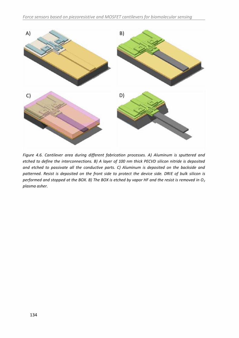
Force sensors based on piezoresistive and MOSFET cantilevers for biomolecular sensing
134
Figure 4.6. Cantilever area during different fabrication processes. A) Aluminum is sputtered and
etched to define the interconnections. B) A layer of 100 nm thick PECVD silicon nitride is deposited
and etched to passivate all the conductive parts. C) Aluminum is deposited on the backside and
patterned. Resist is deposited on the front side to protect the device side. DRIE of bulk silicon is
performed and stopped at the BOX. B) The BOX is etched by vapor HF and the resist is removed in O2
plasma asher.
D) C)
B)A)

Chapter IV. MOSFET cantilever
135
Figure 4.7. A) SEM micrograph of a chip at the
end of the fabrication process. B) Close-up on the
cantilevers. C) close-up on the MOSFET.
4.2.3 –Fabrication issues
Most of the fabrication issues were similar like in the case of piezoresistive cantilevers
(section 3.2.3): bulk silicon DRIE and BOX etching. However, due to the particular structure
of the MOSFET transducer, they influenced much more the final result and the performance
variation. The DRIE of the bulk silicon has not homogeneous speed across the wafer as
mentioned earlier. This fact provokes that the undercut can vary up to 10 m and it
represents a big issue for MOSFET with “short” channel of 10 m or 20m. The result is that
the channel can be in the zone of maximum stress (Figure 4.8.A,C) or in a part of almost zero
stress (Figure 4.8.B,D) because the silicon and BOX underneath are not etched, resulting in a
very big sensitivity variation (section 4.3.4).
In a similar way, the sensitivity can be also affected by problems in BOX etching (section
4.3.4). The relative distance between the neutral axis and the channel can be affected, when
the oxide is not completely etched underneath the transistor, like in the case of wafer 4972-
9 (Figure 4.9.A,B). On the other hand, if the BOX etching is performed for too long time,
there is the risk of damage the aluminum gate, as it happened in the other wafers of the
RUN 4972.
C)
B) A)
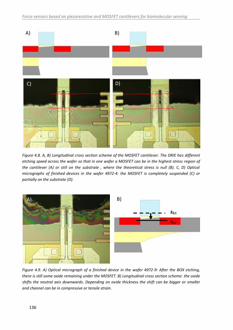
Force sensors based on piezoresistive and MOSFET cantilevers for biomolecular sensing
136
Figure 4.8. A, B) Longitudinal cross section scheme of the MOSFET cantilever. The DRIE has different
etching speed across the wafer so that in one wafer a MOSFET can be in the highest stress region of
the cantilever (A) or still on the substrate , where the theoretical stress is null (B). C, D) Optical
micrographs of finished devices in the wafer 4972-4: the MOSFET is completely suspended (C) or
partially on the substrate (D).
Figure 4.9. A) Optical micrograph of a finished device in the wafer 4972-9: After the BOX etching,
there is still some oxide remaining under the MOSFET. B) Longitudinal cross section scheme: the oxide
shifts the neutral axis downwards. Depending on oxide thickness the shift can be bigger or smaller
and channel can be in compressive or tensile strain.
z0,r
z0,t
B) A)
D) C)
B) A)

Chapter IV. MOSFET cantilever
137
In order to study and improve the piezoresistive and noise properties of MOSFETs in a
more reliable way, my suggestion is to fabricate and perform these studies in structures that
are much easier to fabricate.
4.3 – Characterization
In this section, mechanical, electrical and electromechanical characteristics of the
cantilevers with embedded MOSFET transistors will be presented. The set up for the on-
wafer measurements have been already presented in the previous chapter, therefore here
we will just point out the differences.
4.3.1 – Mechanical characterization
Also in this case, like in the case of the cantilever with embedded piezoresistor, it was
not possible to measure directly the spring constant, due to the fact that the probes were
very soft. They have been calculated, therefore, using the eq. (2.47)-(2.52). Length and width
of the cantilevers were measured by using optical and SEM microscopes and the thicknesses
by the optical interferometer. Young’s moduli of the silicon, silicon oxide, aluminum and
silicon nitride were considered to be ESI= 130 GPa [7], ESIO2= 75 GPa [8-11], EAl=70 Gpa [12,
13] and ENit=70 Gpa. Here below, in Table 4.3, the spring constant are calculated for the
different probe designs. The cantilever A-1 has been simulated by FEM (Ansys, Figure 4.10)
and the spring constant agrees well with the calculated one being around 2.9% lower than
the one estimated by the analytical model. In view of this difference, we don’t make big
error by considering a constant oxide thickness in the multilayer part of the cantilever
(section 4.1.1).
design sub-design kC [mN/m] kC* [mN/m] (kC
* - kC)/ kC
A 1 3.57 3.47 -2.9%
2 0.35 - -
3 5.37 - -
4 0.53 - -
B 1 3.03 - -
2 0.33 - -
3 4.55 - -
4 0.49 - -
Table 4.3. Spring constant of the different cantilever designs by analytical model (kC) and by
simulation (kC*). It has been calculated considering literature values of the Young’s moduli of Si, SiO2
and Al. The Young’s modulus of the silicon nitride has been measured (section 3.3.1).

Force sensors based on piezoresistive and MOSFET cantilevers for biomolecular sensing
138
Figure 4.10.A) Deflection of the cantilever under
a static load of 1 nN. The cantilever bends 288
nm and therefore the kC*=3.47 mN/m. B) Cross
section of the multilayer part of the cantilever
representing the equivalent stress. C) The white
line represents the locus where the stress is
minimum 0 Pa (i.e. neutral axis). It is placed at
z+98 nm respect to the silicon-oxide interface.
4.3.2 – Electrical characterization
The electrical characteristics of the MOSFET transistors were measured using a
semiautomatic probe system Karl Süss PA200 and a semiconductor parameter analyzer
HP4155. The drain current (ID) was recorded as a function of the voltage between source and
drain (VDS) for several gate voltages (VGS) (Figure 4.11.A,B). Additionally, ID was recorded
sweeping VGS between -0.5 and 2 V for a fixed VDS = 0.2 V (Figure 4.11.C,D) in order to
determine the threshold voltage VT. In Table 4.4 we report the average values and standard
deviations for the different MOSFET designs.
ID,sat [A] at VG=4V
wafer 4972-4
SD. [A] ID,sat [A] at VG=4V
wafer 4972-9
SD. [A]] ID,sat of 4972-4/
ID,sat of 4972-9
A1 68 10 (15%) 40 3 (8%) 1.7
A2 62 6 (10%) 39 7 (18%) 1.6
A3 88 9 (10%) 48 8 (17%) 1.8
A4 86 9 (10%) 58 6 (10%) 1.5
B1 140 37 (26%) 61 16 (26%) 2.3
B2 139 27 (19%) 68 17 (25%) 2.0
B3 159 39 (25%) 85 17 (20%) 1.9
B4 141 35 (25%) 100 15 (15%) 1.4
Table 4.4. Averaged saturation drain current for a gate voltage of 4 V in wafer 4672-4 and 4972-9.
Standard variation (SD.) is reported in absolute and (relative) values.
A) B)
C)

Chapter IV. MOSFET cantilever
139
The ID,sat, increases by decreasing the gate length. For example, if we compare the
transistors A1 and B1 of the wafer 4972-4 with a channel length of 20 m and 10 m
respectively, the ID,sat , at VGS=4 V, increases from 68 A to 140 A, which is two times
higher, as expected (2.64). We can notice, also, that the current increases if the source and
drain are formed just by implantation (designs 3 and 4) respect to the design 1 and 2 in
which the source and drain are formed by implantation and dry etching. This fact does not
have a clear origin. Finally the transistors from the wafer 4972-4 have almost two times
higher drain current compared to the transistors of the wafer 4972-9 and it is consequence
of a lower threshold voltage (Figure 4.11.C,D). This difference shouldn’t be related to the
different annealing conditions, which is the only nominal difference between the two
wafers. After the oxide growth, the wafer 4 was annealed further at 900: C for 60’ while the
wafer 9 was annealed at 1050: C for 30’. The difference could be due, more probably, to
different oxide thickness as consequence of the gate oxide etching during the processing, for
example.
0 1 2 3 4 5 6 7
0
20
40
60
80
100
I D [A
]
VDS
[V]
A)
0 1 2 3 4 5 6 7
0
10
20
30
40
50
60
B)
I D [A
]
VDS
[V]
0 1 2 3
0
1
2
3
4
5
6
C)
I D [A
]
VGS
[V]
0 1 2 3
0
1
2
3
4
D)
I D [A
]
VGS
[V]
Figure 4.11. A,B) ID vs. VDS measurements for different VGS (VGS =0, 1, 2, 3, 4 V) for wafers 4972-4 and
4972-9 respectively. C,D) ID vs. VG at constant VDS=0.2 V for wafers 4972-4 and 4972-9, respectively.
Design A4.
Force sensors based on piezoresistive and MOSFET cantilevers for biomolecular sensing
140
The saturation currents present a relatively high relative standard deviation, which is in
between 8% and 26% for the best and the worst case respectively. The variation is between
1.5 and 4 times higher than in the piezoresistive case. This result was expected because the
integration of transistors with a channel width of 4 m and a length of 10m or 20 m is
much more challenging than the integration of a comparable resistor. In fact, we have to
consider that the resolution limit of the photolithography is around 2 m with an overlay
tolerance of 1 m. This fact can explain also that the standard variation (Table 4.4) of the
characteristics is lower for transistors with longer channel (designs A), and higher for
transistors with shorter channel (designs B). Another source of variations can derive from
the fact that the gate oxide is partially etched by wet etching before the metallization. Even
though the wet etching is performed just for 20´´ this can lead to bigger variation of the gate
thickness from chip to chip.
4.3.3 – Noise
The noise power spectral density (PSD) was measured using a low noise current amplifier
(LNA) (SR570 from Stanford Research) and a spectrum analyzer (SR785 from Stanford
Research). The measurements were performed on-wafer, in the KS PA200 probe station,
contacting the source, drain, gate and substrate by the four probes of the probe station. The
use of these probes, allowed the use of triaxial cables, which provide much better shielding
against the external electromagnetic interferences, respect to the coaxial ones. The LNA was
powered by batteries for low noise operations. The LNA input is a source measurements unit
(SMU) so that it can bias the device under test (DUT) and can measure the drain current at
the same time. The drain and gate were connected to the input of the LNA and were biased
at 4 V (VGS=VDS=4V), so that the transistor was in saturation region. The drain current was
“taken up” by the SMU unit and a DC current, with the same intensity, was subtracted not to
drive the amplifier into saturation (Figure 4.12.A). The sensitivity (or amplification) was fixed
at 100 nA/V, which means that a signal of 100 nA is transformed to a signal of 1 V by the
LNA. This sensitivity allowed having a relatively low amplifier noise of (Figure
4.12.B) and a measuring bandwidth of 2 kHz with a low DC input impedance of 10 k which
is much lower compared to the impedance of the DUTs (i.e. 100 k) [14]. The source and
substrate were biased by the ground of the LNA. After the amplification the signal was
processes and recorded by a dynamic signal analyzer (SRS785). In this way, the set up had a
single physical ground (the one of the SR785) avoiding possible ground loops which could
invalidate the measurements.
After the set up development, and before testing the transistors, amplification and noise
measurement had to be performed to assure the correct performance of the amplifier
because the LNA had several years and new batteries had to be installed. In Figure 4.12.C,
we can see the open circuit current noise of the amplifier, which is comparable to the
amplifier specifications (Figure 4.12.B).
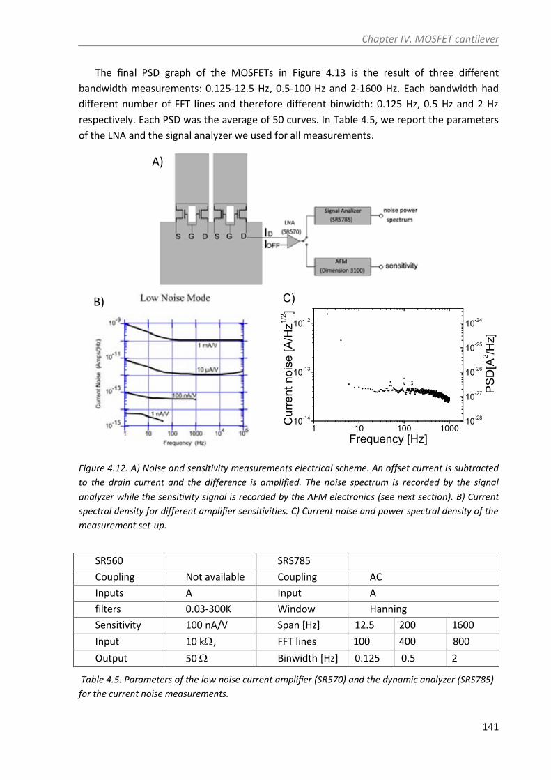
Chapter IV. MOSFET cantilever
141
The final PSD graph of the MOSFETs in Figure 4.13 is the result of three different
bandwidth measurements: 0.125-12.5 Hz, 0.5-100 Hz and 2-1600 Hz. Each bandwidth had
different number of FFT lines and therefore different binwidth: 0.125 Hz, 0.5 Hz and 2 Hz
respectively. Each PSD was the average of 50 curves. In Table 4.5, we report the parameters
of the LNA and the signal analyzer we used for all measurements.
1 10 100 100010-14
10-13
10-12
PS
D[A
2 /Hz]
Cur
rent
noi
se [A
/Hz1/
2 ]
Frequency [Hz]
C)
10-28
10-27
10-26
10-25
10-24
Figure 4.12. A) Noise and sensitivity measurements electrical scheme. An offset current is subtracted
to the drain current and the difference is amplified. The noise spectrum is recorded by the signal
analyzer while the sensitivity signal is recorded by the AFM electronics (see next section). B) Current
spectral density for different amplifier sensitivities. C) Current noise and power spectral density of the
measurement set-up.
SR560 SRS785
Coupling Not available Coupling AC
Inputs A Input A
filters 0.03-300K Window Hanning
Sensitivity 100 nA/V Span [Hz] 12.5 200 1600
Input 10 k, FFT lines 100 400 800
Output 50 Binwidth [Hz] 0.125 0.5 2
Table 4.5. Parameters of the low noise current amplifier (SR570) and the dynamic analyzer (SRS785)
for the current noise measurements.
B)
A)

Force sensors based on piezoresistive and MOSFET cantilevers for biomolecular sensing
142
100
101
102
103
10-24
10-23
10-22
10-21
10-20
P
SD
[A2/H
z]
Frequency [Hz]
Figure 4.13. Power spectral density of the MOSFET from the chip Q11 (design A1) of the wafer 4972-4.
The noise power spectral density in Figure 4.13 was measured on the chip Q11 (design A1) of
the wafer 4972-4. As we can notice, between 1 Hz and 1 kHz, the noise has pure 1/f
behavior, in fact the thermal PSD for this device, and for all the other transistor designs, is on
the order of 10-26 A2/Hz. In Table 4.6, we report the input referred noise values integrated in
the 1 Hz - 1 kHz bandwidth, for 4 different MOSFETS designs in the wafer 4972-4. As
expected, the noise is lower for the transistor with longer channel.
MOSFET design Chip name Channel length
[m]
Integrated noise 1 Hz-10 kHz
[pA]
A1 Q11 20 157 ± 3
A3 I11 20 190 ± 4
B1 L11 10 269 ± 5
B3 H11 10 291 ± 6
Table 4.6. Integrated noise values over the bandwidth 1 Hz-1kHz in 4 different chips.
4.3.4 – Sensitivity and resolution
The displacement and force sensitivities have been evaluated on-wafer, in a similar way
like in the case of the piezoresistive cantilevers by using the AFM and a probe-card. A
different probe-card, compatible with the MOSFET sensor, was design in CNM and
fabricated in HTT.GmbH in Dresden. It was mounted on the micromanipulator on the AFM

Chapter IV. MOSFET cantilever
143
chuck and it could contact all the pads of a single sensor while the AFM was performing a
force curve. A stiff AFM probe (k=40 N/m) was used to deflect the cantilever at a length of
50 m from the clamping edge. The force curve was performed in tapping mode (i.e the
probe was vibrating at the resonance frequency) in order to better evaluate the contact
point between the probe and the cantilever (i.e when the vibration amplitude decays to 0).
Gate and drain were biased at 4 V while source and substrate at 0 V by using the internal
voltage source of the LNA. A LNA internal offset current (IOFF) equal to the drain current, ID,
was selected and the difference ID-IOFF was amplified by a sensitivity of 100 nA/V (Figure
4.12.A).
In Figure 4.14.A,B, we report the displacement sensitivity graphs for the same sensor
Q11 (design A1 with LCH=20 m) from the wafers 4972-4 and 4972-9 and in Figure 4.14.C,D
the deflection of the AFM probe during the sensitivity measurement. As first, we can notice
that the sensitivities have opposite signs. For the chip of the wafer 4972-4, it is negative (i.e.
S= -190±34 nA/m and (ID/ID,0)/ = 0.22±0.04 m-1) while for the chip of the wafer 4972-9
is positive (i.e. S= 165±30 nA/m and (ID/ID,0)/ = 0.38±0.07 m-1). In the first case the
current decreases. This tells us that the channel of the transistor lays below the neutral
plane in a region of compressive stress; in the second case the current increases and
therefore the channel lays above the neutral plane in a region of tensile stress. We can
notice a second difference in the AFM probe deflection: for the cantilever of the wafer 9
(Figure 4.14.D), the AFM probe deflects almost 5 times more than the cantilever of the wafer
4 (Figure 4.14.C). This means that the MOSFET cantilever is much stiffer in the wafer 9. These
two differences cannot be explained by the different thermal treatment performed, which is
the only nominal difference during the wafer processing. On the other hand, they can be
explained easily by watching the Figure 4.8 Figure 4.9. In the wafer 9, at the end of the
process there is still some buried oxide present under the cantilever. This stiffens the
cantilever and modifies the position of the neutral plane (Figure 4.9.B) so that the channel
lays above the neutral plane in a region of tensile stress and therefore ID>0. In wafer 4972-
4 there is no oxide below the cantilever so that the cantilever is softer and the channel lays
below the neutral plane in a region of compressive stress and therefore ID<0. In this case
the position of the neutral plane is at z0,CH=+ 84 nm (eq. (2.47))(the z origin is considered to
be at the silicon surface where the channel is). We simulated the position of the neutral
planes by FEM analysis. The simulated position, i.e. z0,CH*=- 98 nm (Figure 4.10.C), agrees well
with the analytical model as the difference of +14 nm correspond to 1.5% of the total
cantilever thickness. Considering the measured sensitivity of the chip Q11 of the wafer 4, we
can calculate the piezoresistive coefficient of the n-channel (4.4) considering L2=50 m):
and a tip sensitivity (considering L2=200 m):

Force sensors based on piezoresistive and MOSFET cantilevers for biomolecular sensing
144
The piezoresistive coefficient is similar to the literature values at comparable transverse
electric field (section 2.2.2.3). Taking into account a noise of 160 pA (Table 4.6), we can
estimate a force resolution of:
0.0 0.5 1.0 1.5
0
5
10
15
pro
be v
ibra
tion a
mplit
ude [
nm
]
probe z-displacement [m]
diffe
rential outp
ut
curr
ent
[nA
]
A)
-150
-100
-50
0
50
100
0.0 0.5 1.0 1.5
0
5
10
15
pro
be v
ibra
tion a
mplit
ude [
nm
]
probe z-displacement [m]
diffe
rential outp
ut
curr
ent
[nA
]
-100
-50
0
50
B)
0.0 0.5 1.0 1.5
0
5
10
15
C)
pro
be d
eflection [
nm
]
probe z-displacement [m]
0.0 0.5 1.0 1.5
0
20
40
60
80
D)
pro
be d
eflection [
nm
]
probe z-displacement [m]
Figure 4.14. A,B) Sensitivity measurement of chip Q11 in the wafer 4972-4 and 4972-9 respectively.
The sensitivities S= -190±34 nA/m and S= 165±30 nA/m are calculated taking into account the
deflection of the AFM probe. The standard deviation is calculated considering that the measurement
is performed pushing the cantilever at a length of 50±3 m. C,D) Deflection of the AFM probe during
the measurements.
The theoretical sensitivity, noise and resolution according to the model, calculated in Table
4.1, were respectively, SF,I = -0.67, ID,H = 184 pA and MDF = 277 pN. The theoretical sensitivity
is 26% lower than the measured one and this derives from a higher measured drain current
(ID = 88 A vs 52 A).
Several sensors in both wafers were characterized and we noticed that the relative
change of the drain current per displacement unit, (ID/ID,0)/, could vary up to 30 times for
both A and B designs. In Figure 4.15, it is reported the sensitivity of the chip G11 with a
design A4 (i.e. LCH=20 m), which is very similar to design A1, and should have also similar
sensitivity. On the contrary, we can see that it has almost 20 times less sensitivity (S≈ 10
nA/m and (ID/ID,0)/ =0.012 m-1). This can be explained vey easily watching the optical

Chapter IV. MOSFET cantilever
145
micrograph of the cantilever (Figure 4.8.C,D). It is possible to see that the transistor channel
lays in part onto the cantilever (around 13 m) and part on the substrate (around 7 m). On
the other hand, for the chip Q11, the MOSFET lays completely on the cantilever in the
position of maximum stress. This issue is due to the different etching speed of the DRIE used
to etch the bulk silicon. As explain previously in section 3.2.3, it is possible to have undercut
differences of up to 10 m between two points in a wafer. Additionally there could be also
some thin layer of buried oxide underneath the cantilever. In fact, also the HF vapor etching
has not homogenous etching speed across the wafer and therefore can happen that some
particles of BOX remain below the MOSFET, reducing the reciprocal distance between the
neutral axis and the channel and therefore the sensitivity. Considering these two particular
fabrication steps, the integration of a very short deflection transducer (i.e. 10 m or 20 m)
is much more challenging than the integration of a long piezoresistor because the sensors
can have very big performance deviation.
Finally, performing the measurement at different points from the clamping edge and on
different sensors across the wafer we noticed also that the drain current could vary in a
sinusoidal way before and during the contact (Figure 4.16). This issue invalidated many
measurements and especially the ones from the cantilever that had less sensitivity. This
signal can be fitted nicely with a sine of period of 1.4 m which is two time higher than the
AFM laser wavelength (=670 nm). This effect could be related to the interference or to the
diffraction pattern of the laser onto the cantilever, which is also the substrate of the
transistor, or onto the gate or drain of the transistor [15, 16]. Nevertheless, refocusing the
laser onto the AFM probe and performing the force curves at 50 m from the clamping edge
(i.e. near the MOSFET) decreased this effect and increased the electromechanical response
respectively (Figure 4.14.A,B and Figure 4.15).
0.0 0.5 1.0 1.5
0
2
4
6
8
10
12
14
pro
be v
ibra
tion a
mplit
ude [
nm
]
probe z-displacement [m]
diffe
rential outp
ut
curr
ent
[nA
]
-12
-10
-8
-6
-4
-2
0
Figure 4.15. Sensitivity measurement of the chip G11 of the wafer 4972-4. The relative current
variation (ID/ID,0)/ =0.012±0.04 m-1 is ten times lower than for the chip Q11 of the same wafer.

Force sensors based on piezoresistive and MOSFET cantilevers for biomolecular sensing
146
0.0 0.5 1.0 1.5
0
5
10
15
44
48
52
56
60
probe z-displacement [m]
diffe
rential outp
ut
curr
ent
[nA
]
pro
be v
ibra
tion a
mplit
ude [
nm
]
Figure 4.16. Drain current variation due to vertical displacement of the probe. The current varies in a
sinusoidal way also before the deflection of the cantilever.
Concluding, taking into consideration a resolution of 19 pN (wafer 4974-4, design 2x250
for a bandwidth of 1 kHz) and 180 pN for piezoresistive and MOSFET cantilevers,
respectively, the first ones offer much better force resolution (> 9 times). However,
considering that the spring constant is almost 6 times lower (i.e 0.62 mN/m and 3.57 mN/m),
for similar k, the MOSFET cantilever would have just 1.6 times lower sensitivity. Finally, in
view of power consumption (1.3 mW and 0.35 mW), MOSFET cantilever can result
advantageous having approximately three times higher resolution than piezoresistive ones.

Chapter IV. MOSFET cantilever
147
Summary and future research directions
Piezoresistive metal-oxide-semiconductor field effect transistors (MOSFET) represent an
alternative to bulk piezoresistor as deflection transducers. Therefore, cantilever with
embedded a MOSFET have been developed at the same time as the cantilever with
embedded piezoresistors.
The aim of the work presented in this chapter was:
the development of the technological processes to obtain force sensors based on
cantilever with embedded piezoresistive MOSFET deflection transducer.
to measure the sensitivity and noise and extract important materials parameters
like the piezoresistive factor of silicon inversion layer.
to compare the performances of MOSFET and piezoresistive cantilever and to
select the best one to be used in biomolecule recognition.
As first, the electromechanical model has been developed in order to optimize the
different variables (i.e. cantilever and MOSFET dimensions). From it, we saw that it is
possible to obtain comparable force resolution like for the cantilevers with embedded
piezoresistors, but relatively thicker SOI wafer should be used (i.e. 1 m thick device layer).
The mask layout and the fabrication process were presented next. The process flow is
very similar to the one used in the production of cantilever with embedded piezoresistors
and therefore they had similar fabrication issues. However, in this case, the issues have
stronger effect on the performance variations: the sensitivity can vary up to 30 times in a
wafer.
The techniques for the electro-mechanical characterization have been presented
together with the results from two wafers. For the best sensor, we measured a sensitivity of
SF,I= - 0.9±0.16 pA/pN and a noise of ID,noise= 157±3 pA (1 Hz- 1 kHz bandwidth), which lead to
a resolution of MDF= 180±32 pN. From the sensitivity measurements, the longitudinal
piezoresistive coefficient for the n-type silicon inversion layer in the <100> direction was
extracted: 11= 82±15 x 10-11 Pa-1. This is in very good accordance with the literature values.
Even though the resolution is almost two orders of magnitude lower than for the
piezoresistive cantilevers, for similar spring constant and similar power dissipation, the
MOSFET cantilever can represent a good alternative.
Considering the higher standard deviation of the electrical characteristics, the strong
effects of the fabrication issues on the performance and in general the more difficult
integration of the MOSFET into the cantilever, respect to a piezoresistor, we decided to
focus all the efforts just on the piezoresistive cantilevers.
Considering that the MOSFET cantilever can represent a good alternative in cantilever
based force sensors and that a deep recent study about the piezoresistive characteristics of
MOSFET transistors is missing, I would suggest an extensive study of the piezoresistivity of
the MOSFET technology at IMB-CNM on structures much easier to fabricate than cantilevers.

Force sensors based on piezoresistive and MOSFET cantilevers for biomolecular sensing
148

Chapter IV. MOSFET cantilever
149
References
1. Akiyama, T., et al., Integrated atomic force microscopy array probe with metal-oxide-
semiconductor field effect transistor stress sensor, thermal bimorph actuator, and on-chip complementary metal-oxide-semiconductor electronics. Journal of Vacuum Science & Technology B, 2000. 18(6): p. 2669-2675.
2. Tark, S.-H., et al., Nanomechanoelectronic signal transduction scheme with metal-oxide-semiconductor field-effect transistor-embedded microcantilevers. Applied Physics Letters, 2009. 94(10): p. 104101-104101-3.
3. Shekhawat, G., S.H. Tark, and V.P. Dravid, MOSFET-embedded microcantilevers for measuring deflection in biomolecular sensors. Science, 2006. 311(5767): p. 1592-1595.
4. Wang, J., et al., 100 n-type metal-oxide-semiconductor field-effect transistor-embedded microcantilever sensor for observing the kinetics of chemical molecules interaction. Applied Physics Letters, 2009. 95: p. 124101.
5. Singh, P., et al., Microcantilever sensors with embedded piezoresistive transistor read-out: Design and characterization. Sensors and Actuators A: Physical, 2011. 171(2): p. 178-185.
6. Li, X., 1/f Noise in MOSFETs, 1993, Technische Universiteit Eindhoven. 7. Wortman, J.J. and R.A. Evans, Young's Modulus, Shear Modulus, and Poisson's Ratio in
Silicon and Germanium. Journal of Applied Physics, 1965. 36(1): p. 153-156. 8. Halg, B. On a nonvolatile memory cell based on micro-electro-mechanics. in Micro
Electro Mechanical Systems, 1990. Proceedings, An Investigation of Micro Structures, Sensors, Actuators, Machines and Robots. IEEE. 1990.
9. Kapels, H., et al. Full Characterization and Long-Term Stability of Standard CMOS Materials for Integrated Micromechanical Applications. in Solid-State Device Research Conference, 1999. Proceeding of the 29th European. 1999. IEEE.
10. Zhao, J.-H., et al., Measurement of elastic modulus, Poisson ratio, and coefficient of thermal expansion of on-wafer submicron films. Journal of Applied Physics, 1999. 85(9): p. 6421-6424.
11. Guohua, W., et al. A Comprehensive Study on Nanomechanical Properties of Various SiO2-Based Dielectric Films. in Microelectronics and Electron Devices (WMED), 2010 IEEE Workshop on. 2010.
12. Kabe, Y., H. Tanimoto, and H. Mizubayashi, Elasticity study of nanostructured Al and Al-Si (Cu) films. Materials Transactions, 2004. 45(1): p. 119-124.
13. Haque, M.A. and M.T. A Saif, Mechanical behavior of 30-50 nm thick aluminum films under uniaxial tension. Scripta Materialia, 2002. 47(12): p. 863-867.
14. Blaum, A., et al., A new robust on-wafer 1/f noise measurement and characterization system. Proceedings of IEEE 2001 International Conference On Microelectronic Test Structures, 2001. 14: p. 125-130.
15. Werner, R., C. Zimmermann, and A. Kalz, Light dependence of partially depleted SOI-MOSFET's using SIMOX substrates. Electron Devices, IEEE Transactions on, 1995. 42(9): p. 1653-1656.
16. Bosch, M.A., D. Herbst, and S.K. Tewksbury, The influence of light on the properties of NMOS Transistors in laser µ-zoned crystallized silicon layers. Electron Device Letters, IEEE, 1984. 5(6): p. 204-206.

Force sensors based on piezoresistive and MOSFET cantilevers for biomolecular sensing
150

Chapter V. Biomolecule recognition
151
Chapter V
5 – Biomolecule recognition
Chapter 5 - Biomolecule recognition 151
5.1 – Set up 153
5.1.1 – PicoLe 5100 AFM 153
5.1.2 – Substrate chip 158
5.2 – Sensitivity and noise in air and liquid 162
5.3 – Cantilever and substrate functionalization 165
5.4 – Single biomolecule recognition 168
Summary and future research directions 173
References 175

Force sensors based on piezoresistive and MOSFET cantilevers for biomolecular sensing
152

Chapter V. Biomolecule recognition
153
Biomolecule recognition
In order to apply the developed sensor to detect biomolecules at single molecule
resolution, we evaluated that the most straightforward was the detection of the
intermolecular forces between ligands and receptors, using the AFS measuring approach.
Preliminary experiments were carried out in IMB-CNM, but due to the lack of knowledge of
this technique, the experiments were not successful: no unbinding event was detected. In
this perspective, it was of key importance to start an intensive collaboration with a group
that had strong knowledge on this subject, in order to learn the AFS technique, integrate the
piezoresistive sensor in an AFM and to perform AFS experiments with the new set up.
Therefore, after a positive answer from Prof. Salvatore Cannistraro of the Biophysics and
NanoScience center at Tuscia University of Viterbo, Italy, I obtained a COST action
scholarship that financed me a short stay of three months in his lab.
In this section, the set-up (AFM and substrate sample) used in the experiments; the
sensitivity and noise measurements; the functionalization procedures and finally the
successful detection of the unbinding forces related to the biomolecule recognition between
neutravidin and biotin molecules are presented.
5.1 – Set up
In the previous chapter 3, we showed that we achieved force sensors, which are capable
of sub-10 pN resolution in liquid environment (see also section 5.2). These are appropriate
to study the interaction involved in the formation of a molecular complex using the AFS
measuring approach. For this purpose highly controlled displacements during the F-z curves
are needed. In collaboration with the research group headed by Prof. Salvatore Cannistraro,
we decided to integrate the sensor into a PicoLe 5100 AFM, from Agilent Technologies, to
take advantage of the high mechanical stability of this equipment and the highly reliable
displacement of the piezo actuator. Even though we choose this microscope, the sensors can
be easily integrated in other AFMs, as for example we did in the Cervantes fullmode AFM
from Nanotec Electronica S.A. The pre-requisite is that the AFM has a break-out box by
which the deflection signal from the position sensitive photodiode can be substituted by the
differential output voltage of the integrated deflection transducer of the piezoresistive
sensor.
5.1.1 – PicoLe 5100 AFM
In order to use our sensor in the PicoLe 5100 AFM we had to mechanically and
electronically integrate the chip into the microscope.

Force sensors based on piezoresistive and MOSFET cantilevers for biomolecular sensing
154
The commercial probe holder (also called nose cone) of the PicoLe uses a clip to hold
firmly a standard AFM chip. Unfortunately, this was not suitable to hold the chip without
causing any damage to sensitive parts of the encapsulated die (i.e nitride passivation or wire
bonding). In this perspective, a custom AFM nose cone was designed and made by rapid
prototyping at IMB-CNM (Figure 5.1.A,B). The silicon dies were glued and ultrasonically wire
bonded on a custom made 0.4 mm thick printed circuit board (PCB) (Figure 5.1.C). On the
PCB backside, it was glued also a 0.1 mm magnetic thick steel sheet. All the conductors were
passivated by a mono component room temperature curable silicone coating (3140 RTV
from Dow Corning®). The board was held firmly by a neodymium magnet embedded in the
nose cone and inserted into a low profile zero insertion force (ZIF) connector (Figure
5.1.A,B,C). Thanks to this new design, the positioning of the sensor was much easier, with no
danger to damage the chip during the mounting process and at the same time very stable.
The concept of the developed set-up was to simplify and to make as small as possible
the path from the sensor to the electronic equipment. For this purpose, the ZIF connector
with the lowest profile available in the market was selected (54550-0694 from Molex). This
connector is very small (4.7 mm x 3.6 mm x 1mm) and has 6 pins with a pitch of 0.5 mm.
Normally, they are used to create electrical connection with Flat Flexible Cable (FFC), which
have a thickness of 0.3 mm, however we could insert the PCB, which is 0.4 mm thick,
without any problem or drawback. Choosing this connector allowed us to downscale sensibly
also the PCB dimensions: 15 mm x 3.7 mm x 0.4 mm. Due to the reduce weight of the PCB
and of the connector, the magnetic force between the small magnet (N35D34 from
laboutiquedeliman.com with a diameter of 3 mm and a height of 4 mm) and the thin iron foil
(10 mm x 3.5 mm x 0.1 mm) was sufficient to guarantee high stability during the AFS
measurements. The 3140 RTV silicone coating used to passivate all the metallic parts,
inclusive the wire bondings, was chosen because it has high dielectric constant, is mono-
component, does not require heat for curing, and has good thixotropic properties: it
behaves as viscous under static conditions but flow relatively easy under shear stress. These
characteristics are excellent in order to easily make a good quality passivation with a very
low profile with no risk to damage the wirebondings (Figure 5.1.C). In Figure 5.2.A-D, then
we can see the nosecone mounted into the AFM head, the substrate chip (see next section)
placed into the fluid cell on the sample holder and the final assembly.
Regards to the electronic integration, unshielded copper cables with a diameter of 0.25
mm (Kynar) and a length of 15 cm were soldered at the terminals of the ZIF connector and
glued by an epoxy resin (5-minutes Epoxy from Araldite) to improve the strength of the
connection (Figure 5.1.B). The wires were shielded altogether by aluminum foil and at the
other terminal we soldered a standard 6 position header with a pitch of 1.25 mm (Molex). In
this way the cables could be connected easily to a “coaxial box” (Figure 5.2.D). This box was
developed to null the differential output voltage of the sensor, using two wirewound
potentiometers (1 k from Bourns) (Figure 5.2.E) and to pass the signals from unshielded
cables to shielded BNC cables. For future experiments, I would suggest to use an on-board

Chapter V. Biomolecule recognition
155
low noise amplifier that can be integrated into this box, which it has been already designed
and is under production. The coaxial box was then connected to the external low noise
amplifier (SR560 from Stanford Research) with two 50 cm long BNC cables. The sensors were
biased by 4 AA rechargeable batteries (Eneloop - Sony) that provided a low noise constant
voltage of 5 V. The output differential voltage was amplified 2000 times and low pass filtered
at 10 kHz. The resulting signal was used as feedback to approach the cantilever to the
sample substrate. To this purpose we introduced the amplified piezoresistive signal into the
“error signal” of the controller via the break out box, which is a device that allows to monitor
or change the internal signals between the AFM and the controller (Figure 5.2.E). Under
normal working conditions the error signal, is the signal coming from the photodetector
related to the deflection of the cantilever.

Force sensors based on piezoresistive and MOSFET cantilevers for biomolecular sensing
156
Figure 5.1. A) Top, lateral and isometric views of the custom AFM nose cone design. B) Nose cone
made by rapid prototyping with a chip install onto it. C) Front, side and back view of the die wire
bonded on the PCB and passivated by silicone. In the top view the PCB is inserted into the ZIF
connector. The red cables are soldered on the ZIF terminals and epoxy resist is applied to strength the
connections. The cables are shielded altogether by aluminum foil. In the side view we can appreciate
the height of each components: the PCB is 0.4 mm thick and the die is 0.5 mm thick. The passivation
of the wire bonding has to be as thin as possible to avoid any interaction with the substrate when the
chip is mounted on the AFM. On the back view, a steel foil glued on the PCB is visible.
C)B)
A)

Chapter V. Biomolecule recognition
157
Figure 5.2. A) The nose cone is installed in the AFM head. B) The fluid cell and the substrate chip are
placed on the sample holder. C) Design of the assembly with all the components. The PCB, which is
inserted in the ZIF connector, is held by the magnet embedded into the nose cone. The nose cone is
inserted into the AFM head. The fluid cell and the substrate chips are placed beneath the nose cone.
D) Picture of the final set up. Up is visible the optical microscope of the AFM. Below there is the AFM
head and in front there are the coaxial box with the potentiometers and the batteries. E) Electrical
scheme of the set up. The Wheatstone bridge can be balanced by 2 potentiometers. The output
differential voltage is amplified by a low noise voltage amplifier and is introduced into the AFM
controller by the break out box (BOB). This signal substitutes the error signal coming from the
photodiode, related to the deflection of the cantilever and normally used to approach the cantilever
to the substrate.
E)
D) C)
B) A)

Force sensors based on piezoresistive and MOSFET cantilevers for biomolecular sensing
158
5.1.2 – Substrate chip
In this section we will discuss the microfabrication of the substrate chips with sharp tips
for the molecule atomic force spectroscopy measurements. As it is pointed out in the
introduction (chapter 1.4) it is of key importance that just small areas between the
cantilever and the substrate interact during this measurement to allow the interaction of
just few molecules. In standard AFS measurements the typical AFM probes have a tip radius
of 50 nm, while the substrate is a flat glass substrate. In our case the cantilevers don’t have a
real tip because we started from SOI device layer of 340 nm in order to optimize the
resolution. We could have started from a thicker SOI wafer but the microfabrication of a tip
would have made the process far more complex. Additionally thicker SOI wafer have also
higher thickness standard deviation which would have been an issue for nano-thick
cantilevers. However, it is not strictly needed to fabricate a sharp tip perpendicular to the
cantilever but it could be microfabricated also in-plane, as reported by other researchers [1].
I would suggest this option for the future.
A set of two masks was designed.
1. The fist mask (Figure 5.3.A) is used to define a round area for the tip and a bigger
area which has a U shape and can be used as visual reference for optical
alignment during AFS measurements (see next paragraphs). The tip area is a circle
with a diameter of 3 or 5 m.
2. The second mask (Figure 5.3.B) is used to define pillars with a squared cross-
section of 50x50 m or 30x30 m and the same U-shaped reference.
In Figure 5.3.C, we reported the masks overlapping for a single chip, which has the
following dimensions: 10 mm x 5 mm.
The process [2] starts with a 500 m thick p-doped silicon wafer with a resistivity of 1-10
cm (Figure 5.4.A). A layer of approximately 1 m of oxide was deposited via
tetraethylorthosilicate(TEOS)/O2-plasma enhanced chemical vapor deposition (PECVD) at
400º C in the Applied Materials Precision 5000 CVD equipment. The first photolithography, is
performed to define the tip area and the oxide is etched via CHF3/C2F6 reactive ion etching
(RIE) in Drytek QUAD 484 etcher (OXI-QUAD conditions) (Figure 5.4.B). Afterwards, a layer of
6 m of resist is spinned and the second photolithography is performed to define the mask
for the pillars (Figure 5.4.C). Using the resist as etching mask, 100 m of bulk silicon are
etched via SF6/C4F8 Bosch deep reactive ion etching process (DRIE) in an Alcatel 601 etcher
(P601DEEP conditions) (Figure 5.4.D). After the cleaning in an O2 plasma asher, a series of
two DRIE in the Alcatel 601 is performed. The first etching is somehow “isotropic”, it has a
horizontal: vertical etching ratio of 1:2 and is used to etch horizontally the silicon
(NANO2BISMOD conditions) (Figure 5.4.E-F). After measuring the vertical etching speed (2
m/min), we etched the wafer for 2’20”. During this step almost all the silicon under the
oxide disk is etched and a proto-tip is formed. We stopped the process just after the first
oxide protective disks fall down in the external part of the wafer (Figure 5.5.C). This happens

Chapter V. Biomolecule recognition
159
because not all the disks have the same dimensions due to deviations in the
photolithographic process and because the etching speed can vary around 6% across the
wafer. The second etching (NANO1 conditions) is highly anisotropic and is used to vertically
etch the tip for 5 m, using the oxide disk as mask (Figure 5.4.G-H). Then, oxidation of 400
nm at 1100:C (Figure 5.4.I-L) and oxide etching by SiOetch solution (Figure 5.4.M-N, Figure
5.5.D-F) are performed to obtain a sharper apex. A final oxide of 50 nm is grown at 1000:C
to protect the tip. After the end of the microfabrication, the wafers are protected by hard
backed photoresist and saw cut.
Figure 5.3. A) Detail of the mask to define the tip region and U reference area. B) Mask to define the
pillar and the U reference area. C) Overlapping of the 2 mask levels for a single chip: there are four
rows of tips on pillars, two with and two without U reference.
C)
B) A)

Force sensors based on piezoresistive and MOSFET cantilevers for biomolecular sensing
160
N) M)
L) I)
H) G)
F)E)
D) C)
B) A)
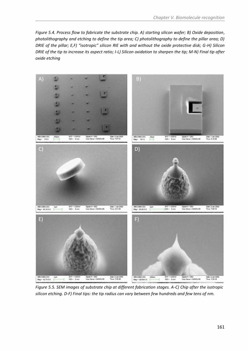
Chapter V. Biomolecule recognition
161
Figure 5.4. Process flow to fabricate the substrate chip. A) starting silicon wafer; B) Oxide deposition,
photolithography and etching to define the tip area; C) photolithography to define the pillar area; D)
DRIE of the pillar; E,F) “isotropic” silicon RIE with and without the oxide protective disk; G-H) Silicon
DRIE of the tip to increase its aspect ratio; I-L) Silicon oxidation to sharpen the tip; M-N) Final tip after
oxide etching
Figure 5.5. SEM images of substrate chip at different fabrication stages. A-C) Chip after the isotropic
silicon etching. D-F) Final tips: the tip radius can vary between few hundreds and few tens of nm.
F) E)
D) C)
B) A)

Force sensors based on piezoresistive and MOSFET cantilevers for biomolecular sensing
162
5.2 – Sensitivity and noise in air and liquid
In this section F-z curves and noise measurements of sensors from wafer 6481-3 and
6481-4 will be presented. While the sensors from the wafer 3 performed very good, there
were some issues related to chips from wafer 4.
The sensors (wafer 6481-3) were tested in air, de-ionized water (milli-Q water) and PBS
(phosphate buffer saline solution) for several hours in order to verify their performance in
liquid medium by using the new set-up. Several F-z curves were recorded in order to
calculate their sensitivity (Figure 5.6.A). In the Picole AFM, the set point to engage the
cantilever to the substrate is fixed and it is 0 V. We found that unbalancing the bridge to
start the engage procedure with -2 V in air and -0.1 V in liquid could lead to reliable
engaging. The motor displaced the substrate until the signal increased to 0 V. This means
that the signal from the chip varies around 1 mV in air and just 50 V in water, considering
that the signal is amplified 2000 times. Somehow the cantilever in air deflects already before
engaging the substrate. This is probably due to potential difference between the cantilever
and the substrate and to the water meniscus formation at the contact point between the
cantilever and the substrate. Figure 5.6.A shows the typical difference between the F-z
curves in air and in liquid environment for the cantilevers of the wafer 6481-3. During the
approach in air, there is a jump-to-contact preceded by a region of attractive forces. During
the retraction, the restoring force of the cantilever does not exceed the adhesion force and
therefore the cantilever remains in contact [3]. In water, instead, there is neither jump-on-
contact nor jump-off-contact. As expected, no significant sensitivity variation in liquid
respect to air was observed, i.e. 354 V/m and 359 V/m, respectively.
Figure 5.6. (A) F-z measurement in air (black and red curves) and water (blue and light blue).
Approaching the sample in air, a jump-on contact event is detected (black line). Retracting the
cantilever for 1 m is not sufficient to overcome the adhesion force, therefore there is no jump-off-
contact (red curve). In water, instead, there are no jump phenomena and the sensitivity has no
significant variation. From the slopes we calculated sensitivities of 354 V/m and 359 V/m for air
and water environments, respectively. (B) The peak to peak noise has a value of 18 V in air (between
0 and 6 s) and in grounded PBS solution (between 12 and 18 s). When the solution is not grounded
(between 6 and 12 s) the noise is more than 2 times higher. There is no significant noise variation
between air and grounded PBS.
B) A)

Chapter V. Biomolecule recognition
163
The peak-to-peak noise (Figure 5.6.B) did not change significantly when the liquid was
grounded (ground represented by the batteries ground). If the water had floating potential,
we noticed instead a relevant increase in the 50 Hz peaks with noise average level rising
from 18 V to 42 V. Such low noise of the set up is due to the good nitride cantilever
passivation on one side, and to the fact that the AFM provide a good shielding against the
electromagnetic external interferences (Figure 5.2). These sensitivity and noise values are in
good agreement with the values extracted from the on-wafer characterization.
In Figure 5.7.A, we report typical F-z curves in air of a sensor from the wafer 6481-4. This
curve shows a very strange behavior of the cantilever in contact with the substrate. In the
approach curve we cannot see a precise contact point; instead the slope varies continuously,
between z=+200 nm and -200 nm, until a constant slope of 550 mV/m is reached between
z=-200 nm and z=-800 nm. At z= -800 nm the signal decay for about 0.4 V and then increases
again with the same slope. In the retract curve, the slope is constant and has the same value
between -900 nm and -600 nm, but then changes continuously. This behavior is probably
due to buried oxide “network” present on the cantilever at the end of the fabrication
process (section 3.2, Figure 3.30). In order to solve this problem we tried to clean the surface
inserting the cantilever tip into a glass microcapillary with a diameter of 90 m (see section
5.3) that was previously filled with 5% HF solution. Even though the HF etches the glass of
the capillary, this could widthstand for several tens of minutes with no damage, due to the
fact that solution was very diluted and had very small volume. After an etching of 2 minutes
we performed again the F-z curve and the graph improved a lot (Figure 5.7.B). Then we
performed an F-z curve in water (Figure 5.7.C) but in the approaching curve were visible two
different slopes. The cantilever tip, probably, was still “dirty” and this was presumably due to
the fact that the HF solution lost the main fluoride content dissolving the glass of the
capillary. However, we used this cantilever for biomolecule recognition experiments (section
5.4), but with no success. We tried to clean several cantilevers in glass capillaries with the
same negative result. We tried also to clean them in plastic micropipettes, but unfortunately
these had bigger diameter (250 m) so that the HF could evaporate on the cantilever and
etch away the silicon nitride; using glass microcapillaries with a diameter <100 m, we didn’t
noticed any evaporation instead.
Out of these experiments, therefore, I would suggest not to use a RIE to release a
cantilever during the fabrication process, because it does not remove completely the oxide
(section 3.2). If cleaning of cantilever should be performed, it should be done in HF resistant
plastic microcapillaries with a diameter of less than 100 m, to reduce HF evaporation.
A second issue encountered in some chip of both wafers was the unreliable passivation
of the aluminum interconnections. In some sensor, the water corroded the aluminum some
minutes after the application of a 5 V bias (Figure 5.8.A). This happened mostly at the height
steps near the contact windows of the chips (Figure 5.8.B). This was probably due to the
aluminum etching issues in the RUN 6481. This is an additional reason to choose lift-off
technique to define the interconnections.

Force sensors based on piezoresistive and MOSFET cantilevers for biomolecular sensing
164
-0.9 -0.6 -0.3 0.0 0.3 0.6 0.90.0
0.1
0.2
0.3
0.4
0.5
approach retract
outp
ut v
olta
ge [m
V]
z [m]
A)
-0.9 -0.6 -0.3 0.0 0.3 0.6 0.90.4
0.5
0.6
0.7
0.8
B)
approach retract
outp
ut v
olta
ge [m
V]
z [m]
-0.9 -0.6 -0.3 0.0 0.3 0.6 0.9-0.05
0.00
0.05
0.10
0.15
0.20C)
approach retract
outp
ut v
olta
ge [m
V]
z [m]
Figure 5.7. Force distance curve of a sensor from wafer
6481-4. A) F-Z curve in air. There is no clear contact
point with the sample, the approach and retract curve
do not have constant sensitivity while the cantilever is
in contact. This behavior is probably due to the buried
oxide left on the cantilever. B) F-z curve in air. After
cleaning the cantilever tip with 5% HF solution, the
cantilever performs better curve. C) F-z curve in water.
The cantilever has still different sensitivity in the
approach curve. Probably the tip is still “dirty”.
Figure 5.8. A) Optical micrograph of a biased sensor immersed in the water. 3 bubbles are visible.
These are due to the aluminum corrosion which release hydrogen. B) It is visible that the aluminum
interconnections are partially corroded.
B) A)
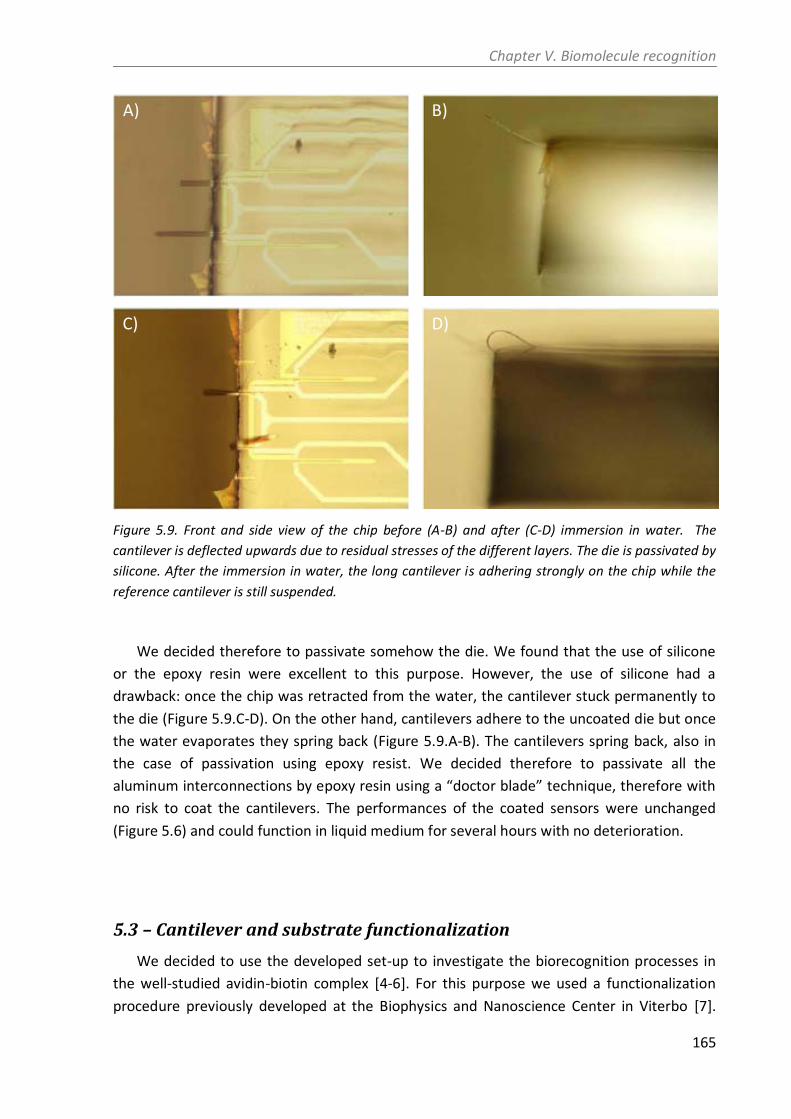
Chapter V. Biomolecule recognition
165
Figure 5.9. Front and side view of the chip before (A-B) and after (C-D) immersion in water. The
cantilever is deflected upwards due to residual stresses of the different layers. The die is passivated by
silicone. After the immersion in water, the long cantilever is adhering strongly on the chip while the
reference cantilever is still suspended.
We decided therefore to passivate somehow the die. We found that the use of silicone
or the epoxy resin were excellent to this purpose. However, the use of silicone had a
drawback: once the chip was retracted from the water, the cantilever stuck permanently to
the die (Figure 5.9.C-D). On the other hand, cantilevers adhere to the uncoated die but once
the water evaporates they spring back (Figure 5.9.A-B). The cantilevers spring back, also in
the case of passivation using epoxy resist. We decided therefore to passivate all the
aluminum interconnections by epoxy resin using a “doctor blade” technique, therefore with
no risk to coat the cantilevers. The performances of the coated sensors were unchanged
(Figure 5.6) and could function in liquid medium for several hours with no deterioration.
5.3 – Cantilever and substrate functionalization
We decided to use the developed set-up to investigate the biorecognition processes in
the well-studied avidin-biotin complex [4-6]. For this purpose we used a functionalization
procedure previously developed at the Biophysics and Nanoscience Center in Viterbo [7].
D) C)
B) A)

Force sensors based on piezoresistive and MOSFET cantilevers for biomolecular sensing
166
Substrates and cantilevers were cleaned by hot acetone, exposed to UV light to expose
hydroxyl groups and then covalently functionalized with biotinylated bovine serum albumin
(b-BSA) and neutravidin, respectively. In both cases the proteins were linked to the
aldehyde groups of the glutaraldehyde that was linked to the amino groups of the (3-
aminopropyl)triethoxysilane (APTES) (Figure 5.10). Non-specific binding sites were blocked
by ethanolamine.
All the starting materials were purchased from Sigma-Aldrich. The PBS used for the
functionalization or washing had a strength of 50 mM with a pH of 7.5. All the cleanings and
functionalizations were performed by immersing the substrate in Petri dishes and the
cantilevers into microcapillaries by using a micromanipulator [8] (Figure 5.11). The
microcapillaries were fabricated starting from standard borosilicate glass capillaries by using
a micropipette puller to achieve a final diameter of 100 m. This diameter is ideal, because
it allows an easy cantilever insertion and the wetting of a small part of the beam. If the
diameter is of 250 m, instead, we found that the cantilever would completely get wet.
At the beginning, substrates and cantilever were washed in acetone for 10 minutes. The
immobilization procedures for both consisted of 5 steps:
hydroxyl group exposure
silanization
linker molecule deposition
receptor, or ligand, coupling
passivation of active linker
CANTILEVER
The hydroxyl groups of the silicon oxide were formed by exposing the cantilevers to UV
light (200W Hg-Xe lamp) for 30 minutes. Subsequently the cantilever were immersed into
freshly prepared 6.3% v/v 99% APTES solution in chloroform for 3 minutes, washed in
chloroform (3 x 5 min) and dried under nitrogen. The linker molecule deposition was carried
out in 1% v/v grade II 25% glutaraldehyde solution in milli-Q water for 3 minutes. Later, the
cantilevers were cleaned in milli-Q water (3 X 5 min) and dried under nitrogen. The
incubation of the receptor was performed overnight via a 10 M neutravidin solution in PBS.
The cantilevers were cleaned in PBS (3 x 5 min) and in milli-Q water (1 x 5 min). The active
sites of the glutaraldehyde that didn’t react with the neutravidin, were blocked by
immersing the cantilevers into 60% wt ethanolamine hydrochloride solution in water for 5
minutes. Finally the cantilevers were washed with PBS and with milli-Q water.
SUBSTRATE
The functionalization of the substrate followed similar steps. The chips were exposed to
UV light for 30 min, immersed in 2% APTES solution in chloroform for 3 hours, washed in
chloroform (3 x 5 min) and dried under nitrogen. Afterwards, they were immersed into 1%
v/v glutaraldehyde solution in milli-Q water for 3 minutes, washed with water (3 x 5 min)

Chapter V. Biomolecule recognition
167
and dried under nitrogen. Finally the samples were immersed into a 10 M biotinylated
bovine serum albumin (b-BSA) solution in PBS, washed with PBS and with water.
Cantilevers and substrate were used for atomic force spectroscopy measurements just
after the functionalization.
Figure 5.10. Immobilization strategies of the substrate (left) and probe (right) functionalization. The
b-BSA and the neutravidin were linked to the aldehyde groups of the glutaraldehyde that was linked
to the amino groups of the (3-aminopropyl)triethoxysilane (APTES).
Figure 5.11. Functionalization of the substrate chips (A) and of the cantilevers (B). The sensor is placed
onto a micropositioner in a optical microscope. On the right is placed a microcapillary with the
functionalization solution. The cantilever is inserted inside the capillary by using the micropositioner.
B) A)

Force sensors based on piezoresistive and MOSFET cantilevers for biomolecular sensing
168
5.4 – Single biomolecule recognition
In this section, the final results of the biomolecule atomic force spectroscopy
measurements and the issues encountered during such experiments are presented.
Just after the functionalization, the sensor and the sample were placed in the nose cone
and in the AFM fluid cell, respectively (Figure 5.1.B, Figure 5.2.A, B). After pouring 500 L of
PBS solution into the cell, the cantilever and the substrate were aligned using the optical
microscope and the micromanipulators of the AFM (Figure 5.12). The cantilever was
subsequently engaged to the sample surface, approached further to the sample for 0.9 m
at a constant speed of 1 m/s for a maximum force of around 500 pN, and after 100 ms,
retracted for 1.8 m at a loading rate of 4.3 nN/s. At the same time the differential output
voltage of the sensor was recorded (Figure 5.13). Hundreds of curves were acquired for each
experiment. In most of them no unbinding event is visible since the retraction curve follows
faithfully the approach curve (Figure 5.13.A). The jump-off event in Figure 5.13.B should be
attributed to a non-specific adhesion between the substrate and the cantilever since the
curve has a constant slope [9]. In Figure 5.13.C, instead, the slope is changing before the
jump-off-contact. In this case, the average unbinding force resulted to be 44 ± 12 pN.
Unbinding forces between 50 pN and 100 pN for biotin-avidin complex and similar loading
conditions have been reported in the literature (Figure 5.14)[4], therefore this value could
arise from specific unbinding events occurring between biotin and neutravidin. Due to the
fact that the probe spring constant is 3 orders of magnitude lower than the one of the
typical probes used in the AFS experiments, the jump-off contact occurs at a length between
200 and 300 nm, which is higher than the literature values [4].
Figure 5.12. The cantilever and the tip of the substrate are aligned using the micromanipulators of
the AFM

Chapter V. Biomolecule recognition
169
Figure 5.13. A-C: AFS curves obtained functionalizing the cantilever by b-BSA and the substrate by
neutravidin. (A) No event is detected. (B) Non-specific event. The slope of the retract curve is
constant before the jump-off. (C) Specific unbinding event between biotin and neutravidin. The slope
of the retract curve varies before the jump off. The unbinding force is around 70 pN. A’-C’: schematic
representation of the three measurements.
C’) C)
B’) B)
A’) A)
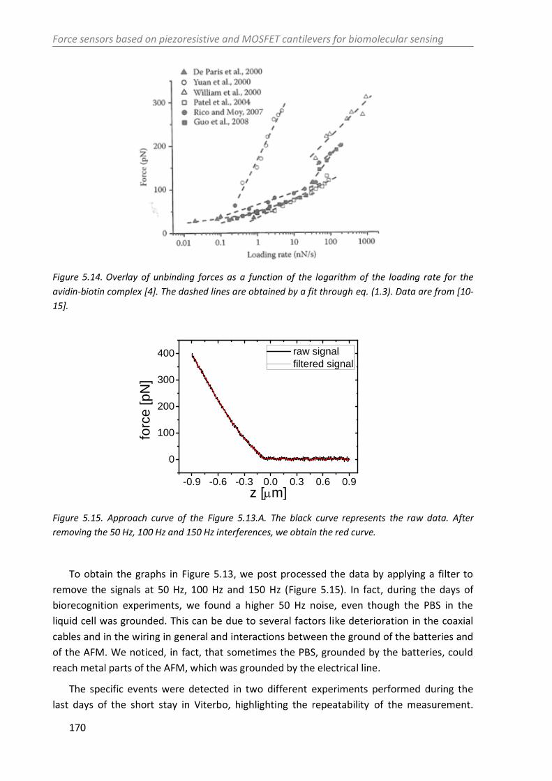
Force sensors based on piezoresistive and MOSFET cantilevers for biomolecular sensing
170
Figure 5.14. Overlay of unbinding forces as a function of the logarithm of the loading rate for the
avidin-biotin complex [4]. The dashed lines are obtained by a fit through eq. (1.3). Data are from [10-
15].
-0.9 -0.6 -0.3 0.0 0.3 0.6 0.9
0
100
200
300
400
raw signal
filtered signal
forc
e [pN
]
z [m]
Figure 5.15. Approach curve of the Figure 5.13.A. The black curve represents the raw data. After
removing the 50 Hz, 100 Hz and 150 Hz interferences, we obtain the red curve.
To obtain the graphs in Figure 5.13, we post processed the data by applying a filter to
remove the signals at 50 Hz, 100 Hz and 150 Hz (Figure 5.15). In fact, during the days of
biorecognition experiments, we found a higher 50 Hz noise, even though the PBS in the
liquid cell was grounded. This can be due to several factors like deterioration in the coaxial
cables and in the wiring in general and interactions between the ground of the batteries and
of the AFM. We noticed, in fact, that sometimes the PBS, grounded by the batteries, could
reach metal parts of the AFM, which was grounded by the electrical line.
The specific events were detected in two different experiments performed during the
last days of the short stay in Viterbo, highlighting the repeatability of the measurement.

Chapter V. Biomolecule recognition
171
Even though we performed several hundreds of force curves, we achieved an overall low
unbinding frequency (n events/total F-Z curves) of ≈3%. This can be due to several facts: not
optimal functionalization procedure for this set up, not perfectly clean cantilever (section
3.2), too low cantilever spring constant, possible denaturation of the molecules due to the
temperature increase and too high electromagnetic interference. In this perspective a study
and simulation about the temperature should be performed; a tip should be integrated into
the cantilever; a dedicated set-up should be developed and the sensor should be integrated
into a microfluid cell; the cantilever should have possibly higher spring constant, in fact the
best AFS results are generally obtained using cantilevers with spring constant around kC=20
mN/m, and this is the first time that AFS experiments are performed with such compliant
cantilever (kC<1 mN/m). About this aspect, further improvements in the microfabrication
process would enable cantilevers with higher spring constant and sub-10 pN resolution.
Finally, it is worth nothing that, in comparison with similar piezoresistive force
cantilevers fabricated by other groups, we offer a probe which is compatible with liquid
media [16], which has higher resolution [17, 18] and it is produced by more straightforward
fabrication process [19, 20].
These results open a new perspective in high sensitive label free biomarkers detection in
nearly physiological conditions. In contraposition with the past, when the mass or the
surface stress caused by the molecule binding to the cantilever was revealed, now we are
able to achieve much higher resolution, down to a single molecule, detecting the
intermolecular force between an analyte molecule and the receptor partner. Even though
this was already possible with the atomic force microscope, the peculiarity of this sensor it is
that the deflection transducer is integrated into the sensors. The sensor, therefore, can be
used with no restrictions in opaque media, it can be easily integrated in microfluidic cells and
displays a high multiplexing potentiality. These characteristics make this force sensor a very
good candidate for a new type of biosensor.

Force sensors based on piezoresistive and MOSFET cantilevers for biomolecular sensing
172

Chapter V. Biomolecule recognition
173
Summary and future research directions
In this chapter the integration of the sensor into a commercial AFM, the substrate chip
fabrication, the functionalization procedure and the biomolecule recognition experiments
have been presented.
In order to perform biomolecule recognition experiments, high mechanical stability and
highly reliable displacements are needed, therefore we integrated the sensor into a PicoLe
5100 AFM, from Agilent Technologies. To this purpose a custom made probe-holder was
designed and made for the correct positioning of the sensor. The piezoresistive deflection
signal was integrated into the AFM electronics by means of a break out box, substituting the
error signal coming from the photodiode.
In the single molecule atomic force spectroscopy experiments, standard AFM cantilevers
with a tip radius of 50 nm are normally used. This is necessary so that just small areas
interact between the cantilever and the substrate. In this way, it is minimized the risk of
multiple bindings of ligand-receptors pairs. Substrate chips with sharp tip have been
therefore fabricated.
Afterwards, we tested the sensors in air and de-ionized water (milli-Q water) for several
hours in order to verify their performance in liquid medium by using the new set-up. The
sensitivity and noise values agree well with the values extracted from the on-wafer
characterization and the sensors were functioning in liquid environment for several hours.
The biomolecular recognition experiments were performed after the functionalization of
cantilevers and substrates with neutravidin and biotin, respectively. We successfully
detected the forces related to the avidin-biotin complex formation, highlighting the
possibility of biomolecule label-free recognition in nearly physiological conditions and at
single molecule resolution. Besides the very high sensitivity attained, the sensor can be used
with no restrictions in opaque media; it can be easily integrated in microfluidic cells and
displays a high multiplexing potentiality. These results, therefore, open a new perspective in
highly sensitive label free biomarkers detection in nearly physiological conditions.
Improvements in the cantilever design as well as in the set up could be made in the
future, as pointed out in the text:
Use of on board amplifier placed near the sensor in order to reduce as much as
possible the external electromagnetic interference.
Fabrication of a tip on the cantilever. This can be out of plane or better in plane
for easier fabrication.
Development of microfluidic systems for better functionalization and easier
detection. This would be the first step towards a real biosensor based on the
detection technique shown in this chapter.
Explore different and maybe easier detection schemes: the pulling of the
molecule may be achieved by means of receptor functionalized magnetic
Force sensors based on piezoresistive and MOSFET cantilevers for biomolecular sensing
174
particles, on which acts a magnetic force [21]. In this case the cantilever doesn’t
need a substrate, so that the system would result simpler.
Chapter V. Biomolecule recognition
175
References
1. Ried, R.P., et al., 6-mhz 2-N/m piezoresistive atomic-force microscope cantilevers with
incisive tips. Microelectromechanical Systems, Journal of, 1997. 6(4): p. 294-302. 2. Villanueva, G., et al., Deep reactive ion etching and focused ion beam combination for
nanotip fabrication. Materials Science and Engineering: C, 2006. 26(2): p. 164-168. 3. Cappella, B. and G. Dietler, Force-distance curves by atomic force microscopy. Surface
Science Reports, 1999. 34(1): p. 1-104. 4. Bizzarri, A.R. and S. Cannistraro, Dynamic Force Spectroscopy and Biomolecular
Recognition2012: CRC Press, Boca Raton. 5. Moy, V.T., E.L. Florin, and H.E. Gaub, Intermolecular forces and energies between ligands
and receptors. Science, 1994. 266(5183): p. 257-259. 6. Izrailev, S., et al., Molecular dynamics study of unbinding of the avidin-biotin complex.
Biophysical Journal, 1997. 72(4): p. 1568-1581. 7. Bizzarri, A.R., et al., Interaction of an anticancer peptide fragment of azurin with p53 and
its isolated domains studied by atomic force spectroscopy. International Journal of Nanomedicine, 2011. 6: p. 3011-3019.
8. Bietsch, A., et al., Rapid functionalization of cantilever array sensors by inkjet printing. Nanotechnology, 2004. 15(8): p. 873-880.
9. Bizzarri, A.R. and S. Cannistraro, The application of atomic force spectroscopy to the study of biological complexes undergoing a biorecognition process. Chemical Society Reviews, 2010. 39(2): p. 734-749.
10. De Paris, R., et al., Force Spectroscopy and Dynamics of the Biotin-Avidin Bond Studied by Scanning Force Microscopy. Single Molecules, 2000. 1(4): p. 285-290.
11. Guo, S., et al., Effects of multiple-bond ruptures on kinetic parameters extracted from force spectroscopy measurements: Revisiting biotin-streptavidin interactions. Biophysical Journal, 2008. 95(8): p. 3964-3976.
12. Patel, A.B., et al., Influence of Architecture on the Kinetic Stability of Molecular Assemblies. Journal of the American Chemical Society, 2004. 126(5): p. 1318-1319.
13. Rico, F. and V.T. Moy, Energy landscape roughness of the streptavidin-biotin interaction. Journal of Molecular Recognition, 2007. 20(6): p. 495-501.
14. Williams, P.M., et al., On the dynamic behaviour of the forced dissociation of ligand-receptor pairs. Journal of the Chemical Society. Perkin Transactions 2, 2000(1): p. 5-8.
15. Yuan, C., et al., Energy landscape of streptavidin-biotin complexes measured by atomic force microscopy. Biochemistry, 2000. 39(33): p. 10219-10223.
16. Harley, J.A. and T.W. Kenny, High-sensitivity piezoresistive cantilevers under 1000 Å thick. Applied Physics Letters, 1999. 75(2): p. 289-291.
17. Aeschimann, L., et al., Scanning probe arrays for life sciences and nanobiology applications. Microelectronic Engineering, 2006. 83(4-9): p. 1698-1701.
18. Polesel-Maris, J., et al., Piezoresistive cantilever array for life sciences applications. Journal of Physics: Conference Series, 2007. 61(1): p. 955-959.
19. Doll, J.C., Advances in high bandwidth nanomechanical force sensors with integrated actuation, 2012, Stanford University.
20. Doll, J.C., et al., Faster than the Speed of Hearing: Nanomechanical Force Probes Enable the Electromechanical Observation of Cochlear Hair Cells. Nano Letters, 2012. 12(12): p. 6107-6111.

Force sensors based on piezoresistive and MOSFET cantilevers for biomolecular sensing
176
21. Baselt, D.R., et al., A high-sensitivity micromachined biosensor. Proceedings of the IEEE, 1997. 85(4): p. 672-679.

Chapter VI. Conclusions
177
Chapter VI
6 – Conclusions
Chapter 6 - Conclusions 177
Perspectives 180
Force sensors based on piezoresistive and MOSFET cantilevers for biomolecular sensing
178

Chapter VI. Conclusions
179
Conclusions
The main objective of this thesis has been the development of a force sensor based on a
self-sensing cantilever compatible with liquid environment endowed with pN force
resolution and its application in biomolecule recognition. In this respect, two different
approaches have been studied: cantilevers with embedded piezoresistors or piezoresistive
MOSFET transistors.
For the cantilevers with embedded piezoresistors, an electromechanical analytical model
has been developed in order to optimize the different parameters to achieve the desired
resolution. According to this model, it is possible to obtain a resolution of less than 10 pN for
a bandwidth of 10 kHz, if the cantilevers have length, arm width and thickness of 250 m,
2m and 325 nm respectively, and a piezoresistor with the following dimensions: 125 m, 2
m and 100 nm. Afterwards, a previously developed fabrication process (developed by Dr.
Luis Guillermo Villanueva) has been improved in order to obtain the desired probes with
high fabrication yield. Different process solutions have been tried and force sensors with
excellent characteristics (resolution of 6 pN and yield of 90%-100%) have been obtained. For
these results, three different key process steps have been optimized. A relatively low
temperature arsenic activation thermal treatment at 950 °C for 75 minutes allowed
obtaining a junction depth of around 100 nm. A combination of dry etching and wet etching
has been used for the back end of line process to avoid any possible damage of the
piezoresistors so to improve the noise characteristics. A custom made HF vapor etcher has
been upgraded to provide fast and homogeneous buried oxide etching across the wafer.
At the same time, the second option of cantilever with an embedded piezoresistive
MOSFET transistor has been explored. The specific two dimensional conduction mechanism
of the transistor can be beneficial to the sensitivity because the conduction is on the surface
of the silicon where the stress is the highest. An electromechanical model has been
developed to evaluate the effect of each variable on the sensitivity and on the noise.
According to this model, good resolution in the order of few tens of pN can be achieved for
cantilever thicknesses of around 1 m. A fabrication process has been developed and
MOSFET with good electrical characteristics have been successfully embedded on
cantilevers. Probes with a resolution of 180 pN for a bandwidth of 1 kHz have been obtained.
Even though, the resolution is worse than piezoresistive cantilevers, it should be pointed out
that the silicon thickness was not the optimal one in this case. According to this result, for
similar spring constant and power consumption, the integration of MOSFET cantilever can
represent a good alternative having 3 times higher resolution with respect to the
piezoresistive cantilever.
Alongside the modeling and fabrication work, much job has been done in the
characterization of the sensors. New set-ups and techniques have been developed in order
to perform highly precise and high-throughput measurements of the noise and sensitivity
characteristics. In view of the success of the project, this has been a very important point. It

Force sensors based on piezoresistive and MOSFET cantilevers for biomolecular sensing
180
has allowed extensive validation of the technological processes involved in production as
well as the characterization of all the devices used in the biomolecular experiments. In
particular, the integration of a probe-card into an AFM has allowed a fast and precise on-
wafer sensitivity measurement and the use of a preamplifier and a spectrum analyzer with a
probe-station have allowed a reliable on-wafer noise characterization. A sensitivity
measurement can be performed in 2 minutes and a noise measurement can last from tenths
of second to several minutes, depending on the requested precision. These new set ups have
allowed the calibration of a considerable number of sensors in a relatively short time and
directly on-wafer. This constitutes a definite improvement with the way these
measurements have been done up to date, where the chip was normally pulled apart from
the wafer, attached on a PCB board and wire bonded, which was a time consuming, risky
and not robust processes. This characterization procedure offers also another advantage
that is the selection of the sensors with better performance before the encapsulation.
During the last months of the experimental work, much effort has been put into the
biorecognition experiments. This part of the thesis has been done in close collaboration with
the research group of the Prof. Salvatore Cannistraro at Tuscia University, in which I have
been hosted for 3 months. The piezoresistive force sensors have been mechanically and
electronically integrated into a commercial PicoLe 5100 AFM to take advantage of the high
mechanical stability of this equipment and the highly reliable displacement of the piezo
actuator. To this purpose a new custom made probe holder has been designed and made for
correct and robust positioning of the PCB, on which the sensor has been encapsulated. A
substrate with very sharp tips has been microfabricated to allow the interaction of very small
areas between the cantilever and the substrate. This fact is essential for single molecule
biorecognition. Finally, we have successfully detected biorecognition specific events
underlying the biotin-avidin complex formation. This result highlights the possibility of
biomolecule label-free recognition in nearly physiological conditions and at single molecule
resolution.
Perspectives
Alongside the text I pointed out some advices about improvement in the sensors and
about future research directions on this topic:
Improvement of the piezoresistive and noise properties of doped bulk silicon (or
of MOSFET) in structures that are much easier to fabricate than cantilevers.
Improvement of the electromechanical model considering the real concentration
profile of the doping atoms. This would require also process simulations and
related experiments.
Fabrication of the chip metal interconnections by lift-off process, avoiding all the
problems associated with the metal etching.

Chapter VI. Conclusions
181
Use a commercial HF vapor etcher to etch in a more uniform way the BOX.
Fabrication of a tip on the cantilever.
Use of low noise specifically designed on board amplifier, to reduce the
electromagnetic external interference during the biomolecular experiments.
Development of microfluidic systems for better functionalization and easier
detection. This would be the first step towards a real biosensor based on the
developed force sensors.
Explore different and maybe easier detection schemes based on the same force
measurement principle.

Force sensors based on piezoresistive and MOSFET cantilevers for biomolecular sensing
182

Appendices
183
Appendices
Appendices 183
Appendix A – Piezoresistive coefficients of MOSFETs 185
References 188
Appendix B – List of publications and participation in conferences 189

Force sensors based on piezoresistive and MOSFET cantilevers for biomolecular sensing
184
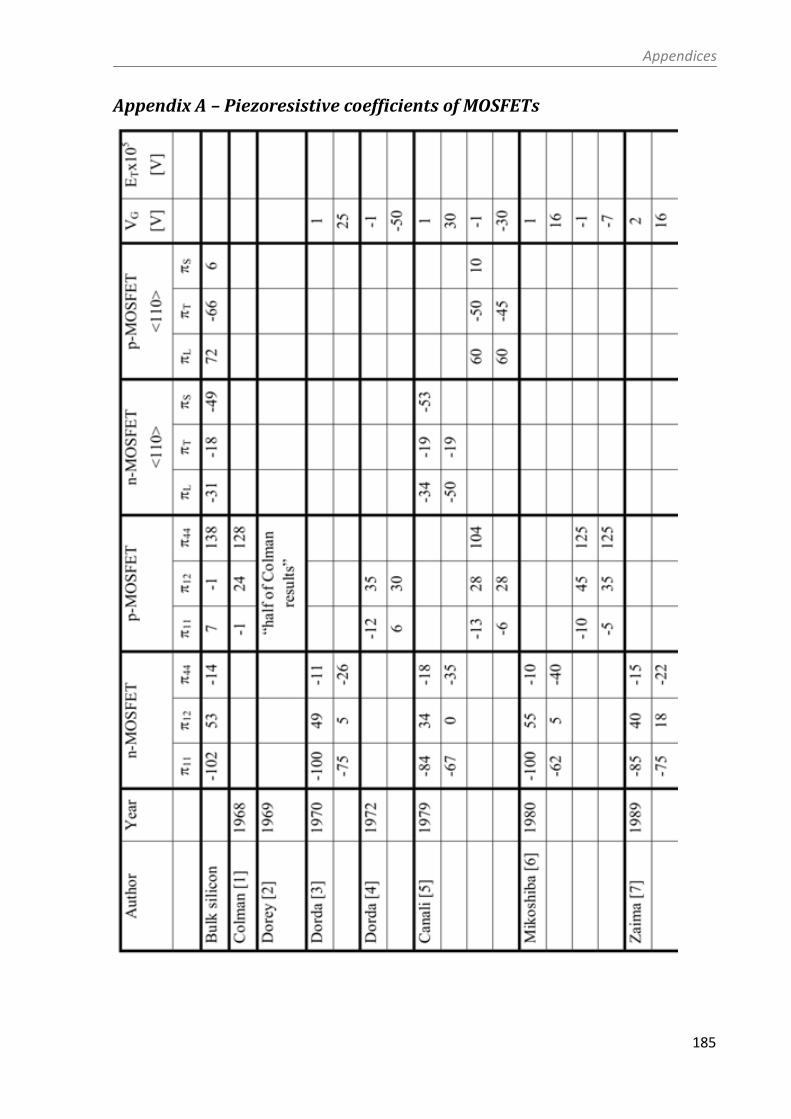
Appendices
185
Appendix A – Piezoresistive coefficients of MOSFETs

Force sensors based on piezoresistive and MOSFET cantilevers for biomolecular sensing
186

Appendices
187

Force sensors based on piezoresistive and MOSFET cantilevers for biomolecular sensing
188
References
1. Colman, D., R.T. Bate, and J.P. Mize, Mobility anisotropy and piezoresistance in silicon p-
type inversion layers. Journal of Applied Physics, 1968. 39(4): p. 1923-1931. 2. Dorey, A.P. and T.S. Maddern, The effect of strain on MOS transistors. Solid State
Electronics, 1969. 12(3): p. 185-189. 3. Dorda, G., Piezoresistance in quantized conduction bands in silicon inversion layers.
Journal of Applied Physics, 1971. 42(5): p. 2053-&. 4. Dorda, G., H. Friedrich, and E. Preuss, Band Structure Investigation on p-Type Silicon
Inversion Layers by Piezoresistance and Mobility Measurements. Journal of Vacuum Science and Technology, 1972. 9(2): p. 759-761.
5. Canali, C., et al., Piezoresistivity effects in MOS-FET useful for pressure transducers. Journal of Physics D-Applied Physics, 1979. 12(11): p. 1973-1983.
6. Mikoshiba, H., Stress-sensitive properties of silicon-gate MOS devices. Solid State Electronics, 1981. 24(3): p. 221-232.
7. Zaima, S., T. Maruyama, and Y. Yasuda, Piezoresistance in n-channel inversion layers of Si MOSFET's. Applied surface science, 1989. 41: p. 433-438.
8. Schorner, R., First and second order longitudinal piezoresistive coefficients of n-type metal-oxide-semiconductor field effect transistors. Journal of Applied Physics, 1990. 67(9): p. 4354-4357.
9. Wang, Z.Z., J. Suski, and D. Collard, Piezoresistive simulation in MOSFETs. Sensors and Actuators A: Physical, 1993. 37-38: p. 357-364.
10. Bradley, A.T., et al., Piezoresistive characteristics of short-channel MOSFETs on (100) silicon. IEEE Transactions on Electron Devices, 2001. 48(9): p. 2009-2015.
11. Gallon, C., et al., Electrical analysis of external mechanical stress effects in short channel MOSFETs on (001) silicon. Solid-State Electronics, 2004. 48(4): p. 561-566.
12. Uchida, K., et al. Experimental study of biaxial and uniaxial strain effects on carrier mobility in bulk and ultrathin-body SOI MOSFETs. in Electron Devices Meeting, 2004. IEDM Technical Digest. IEEE International. 2004.
13. Uchida, K., et al. Physical mechanisms of electron mobility enhancement in uniaxial stressed MOSFETs and impact of uniaxial stress engineering in ballistic regime. in Electron Devices Meeting, 2005. IEDM Technical Digest. IEEE International. 2005.
14. Vatedka, R., et al., Effect of high drain voltage on stress sensitivity in nMOSFETs. Sensors and Actuators a-Physical, 2007. 140(1): p. 89-93.
15. Chang, W.T. and J.A. Lin, Piezoresistive coefficients of <1 1 0> silicon-on-insulator
MOSFETs with 0.135/0.45/10 micrometers channel length with external forces.
Microelectronic Engineering, 2009. 86: p. 1965-1968.

Appendices
189
Appendix B – List of publications and participation in conferences
Peer reviewed articles
1. G. Tosolini, F. Scarponi, S. Cannistraro, and J. Bausells, "Biomolecule recognition using
piezoresistive nanomechanical force probes," Applied Physics Letters, vol. 102, 2013,
pp. 253701-253701-5. DOI: 10.1063/1.4812469.
2. G. Tosolini, L. G. Villanueva, F. Perez-Murano, and J. Bausells, "Fast on-wafer
electrical, mechanical, and electromechanical characterization of piezoresistive
cantilever force sensors," Review of Scientific Instruments, vol. 83, 2012, pp.
015002-015002-7. DOI: 10.1063/1.3673603.
3. G. Tosolini, G. Villanueva, F. Perez-Murano, and J. Bausells, "Silicon microcantilevers
with MOSFET detection," Microelectronic Engineering, vol. 87, 2010, pp. 428-431.
DOI: 10.1016/j.mee.2009.11.125.
Conference proceedings
1. G. Tosolini, L. G. Villanueva, F. Perez-Murano, and J. Bausells, "A novel high-
throughput on-wafer electromechanical sensitivity characterization system for
piezoresistive cantilevers," in IEEE International Conference on Microelectronic Test
Structures, 2012, pp. 55-60. DOI: 10.1109/ICMTS.2012.6190613.
2. G. Tosolini, and L. G. Villanueva, F. Perez-Murano, J. Bausells, "Self sensing cantilevers
for the measurement of (biomolecular) forces," in Electron Devices (CDE), 2011
Spanish Conference on, 2011, pp. 1-4. DOI: 10.1109/SCED.2011.5744171.
3. G. Tosolini, G. Villanueva, and J. Bausells, "Silicon Microcantilevers with Piezoresistive
and MOSFET Detection," Proceedings of the 2009 Spanish Conference on Electron
Devices, pp. 428-431, 2009. DOI: 10.1109/SCED.2009.4800525.
Attendance at conferences
1. G. Tosolini, F. Scarponi, S. Cannistraro, and J. Bausells, "Piezoresistive
nanomechanical force probe in single biomolecule recognition". Poster presentation
at the International Workshop on Nanomechanical Sensing (NMC). 1-3 May 2013,
Stanford, USA.
2. G. Tosolini, J. M. Michalik, R. Cordoba, J. M. de Teresa, F. Perez-Murano, J. Bausells,
"Magnetic properties of cobalt micro-wires measured by piezoresistive cantilever
magnetometry". Poster presentation at the International Conference on Micro and
Nano Engineering (MNE). 16-20 September 2012, Toulouse, France.
3. G. Tosolini, and L. G. Villanueva, F. Perez-Murano, J. Bausells, "A novel high-
throughput on-wafer electromechanical sensitivity characterization system for

Force sensors based on piezoresistive and MOSFET cantilevers for biomolecular sensing
190
piezoresistive cantilevers". Oral presentation at the International Conference on
Microelectronic Test Structures (ICMTS). 19-22 March 2012, San Diego, USA.
4. G. Tosolini, and L. G. Villanueva, F. Perez-Murano, J. Bausells, "Fast and reliable on-
wafer electromechanical characterization technique for piezoresistive cantilevers".
Poster presentation at International Workshop on Nanomechanical Sensing (NMC).
11-13 May 2011, Dublin, Ireland.
5. G. Tosolini, and L. G. Villanueva, F. Perez-Murano, J. Bausells, "Self Sensing
Cantilevers for the Measurement of (biomolecular) Forces". Oral presentation at
Spanish conference on electron devices (CDE). 8-11 February 2011, Palma de
Mallorca, Spain.
6. G. Tosolini, and L. G. Villanueva, F. Perez-Murano, J. Bausells, "Optimization of
piezoresistive and MOSFET cantilever for measuring forces". Oral presentation at
Fuerzas y Tunel Conference. 27-29 September 2010, Tarragona, Spain.
7. G. Tosolini, and L. G. Villanueva, F. Perez-Murano, J. Bausells, "Silicon microcantilever
with MOSFET detection". Poster presentation at International Conference on Micro
and Nano Engineering (MNE). 28 September – 1 October 2009, Ghent, Belgium.
8. G. Tosolini, G. Villanueva, and J. Bausells, "Silicon microcantilevers with piezoresistive
and MOSFET detection". Oral presentation at Spanish Conference on Electron
Devices (CDE). 11-13 February 2009, Santiago de Compostela, Spain.