For Analog Devices ADSP-2191 DSPs (3.3V Supply) Sheets/ST... · 2005-02-04 · For Analog Devices...
61
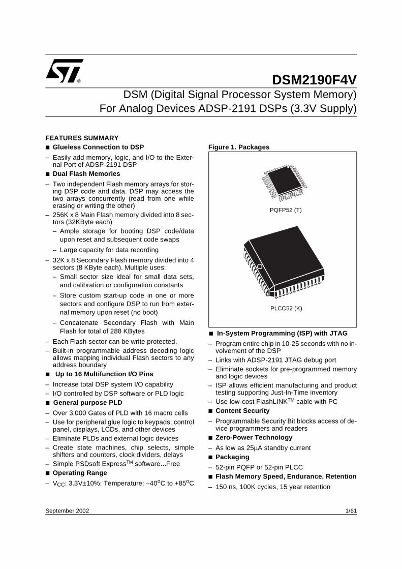
1/61 September 2002 DSM2190F4V DSM (Digital Signal Processor System Memory) For Analog Devices ADSP-2191 DSPs (3.3V Supply) FEATURES SUMMARY ■ Glueless Connection to DSP – Easily add memory, logic, and I/O to the Exter- nal Port of ADSP-2191 DSP ■ Dual Flash Memories – Two independent Flash memory arrays for stor- ing DSP code and data. DSP may access the two arrays concurrently (read from one while erasing or writing the other) – 256K x 8 Main Flash memory divided into 8 sec- tors (32KByte each) – Ample storage for booting DSP code/data upon reset and subsequent code swaps – Large capacity for data recording – 32K x 8 Secondary Flash memory divided into 4 sectors (8 KByte each). Multiple uses: – Small sector size ideal for small data sets, and calibration or configuration constants – Store custom start-up code in one or more sectors and configure DSP to run from exter- nal memory upon reset (no boot) – Concatenate Secondary Flash with Main Flash for total of 288 KBytes – Each Flash sector can be write protected. – Built-in programmable address decoding logic allows mapping individual Flash sectors to any address boundary ■ Up to 16 Multifunction I/O Pins – Increase total DSP system I/O capability – I/O controlled by DSP software or PLD logic ■ General purpose PLD – Over 3,000 Gates of PLD with 16 macro cells – Use for peripheral glue logic to keypads, control panel, displays, LCDs, and other devices – Eliminate PLDs and external logic devices – Create state machines, chip selects, simple shifters and counters, clock dividers, delays – Simple PSDsoft Express TM software...Free ■ Operating Range –V CC : 3.3V±10%; Temperature: –40 o C to +85 o C Figure 1. Packages ■ In-System Programming (ISP) with JTAG – Program entire chip in 10-25 seconds with no in- volvement of the DSP – Links with ADSP-2191 JTAG debug port – Eliminate sockets for pre-programmed memory and logic devices – ISP allows efficient manufacturing and product testing supporting Just-In-Time inventory – Use low-cost FlashLINK TM cable with PC ■ Content Security – Programmable Security Bit blocks access of de- vice programmers and readers ■ Zero-Power Technology – As low as 25μA standby current ■ Packaging – 52-pin PQFP or 52-pin PLCC ■ Flash Memory Speed, Endurance, Retention – 150 ns, 100K cycles, 15 year retention PLCC52 (K) PQFP52 (T)
Transcript of For Analog Devices ADSP-2191 DSPs (3.3V Supply) Sheets/ST... · 2005-02-04 · For Analog Devices...
1/61September 2002
DSM2190F4VDSM (Digital Signal Processor System Memory)
For Analog Devices ADSP-2191 DSPs (3.3V Supply)
FEATURES SUMMARY Glueless Connection to DSP
– Easily add memory, logic, and I/O to the Exter-nal Port of ADSP-2191 DSP
Dual Flash Memories
– Two independent Flash memory arrays for stor-ing DSP code and data. DSP may access thetwo arrays concurrently (read from one whileerasing or writing the other)
– 256K x 8 Main Flash memory divided into 8 sec-tors (32KByte each)– Ample storage for booting DSP code/data
upon reset and subsequent code swaps
– Large capacity for data recording
– 32K x 8 Secondary Flash memory divided into 4sectors (8 KByte each). Multiple uses:– Small sector size ideal for small data sets,
and calibration or configuration constants
– Store custom start-up code in one or moresectors and configure DSP to run from exter-nal memory upon reset (no boot)
– Concatenate Secondary Flash with MainFlash for total of 288 KBytes
– Each Flash sector can be write protected.– Built-in programmable address decoding logic
allows mapping individual Flash sectors to anyaddress boundary
Up to 16 Multifunction I/O Pins
– Increase total DSP system I/O capability– I/O controlled by DSP software or PLD logic General purpose PLD
– Over 3,000 Gates of PLD with 16 macro cells– Use for peripheral glue logic to keypads, control
panel, displays, LCDs, and other devices– Eliminate PLDs and external logic devices– Create state machines, chip selects, simple
shifters and counters, clock dividers, delays– Simple PSDsoft ExpressTM software...Free Operating Range
– VCC: 3.3V±10%; Temperature: –40oC to +85oC
Figure 1. Packages
In-System Programming (ISP) with JTAG
– Program entire chip in 10-25 seconds with no in-volvement of the DSP
– Links with ADSP-2191 JTAG debug port– Eliminate sockets for pre-programmed memory
and logic devices– ISP allows efficient manufacturing and product
testing supporting Just-In-Time inventory– Use low-cost FlashLINKTM cable with PC Content Security
– Programmable Security Bit blocks access of de-vice programmers and readers
Zero-Power Technology
– As low as 25µA standby current Packaging
– 52-pin PQFP or 52-pin PLCC Flash Memory Speed, Endurance, Retention
– 150 ns, 100K cycles, 15 year retention
PLCC52 (K)
PQFP52 (T)
DSM2190F4
2/61
TABLE OF CONTENTS
Summary Description . . . . . . . . . . . . . . . . . . . . . . . . . . . . . . . . . . . . . . . . . . . . . . . . . . . . . . . . . . . . . . 4
Architectural Overview . . . . . . . . . . . . . . . . . . . . . . . . . . . . . . . . . . . . . . . . . . . . . . . . . . . . . . . . . . . . . 6
DSP Address/Data/Control Interface. . . . . . . . . . . . . . . . . . . . . . . . . . . . . . . . . . . . . . . . . . . . . . . . . 6
Main Flash Memory . . . . . . . . . . . . . . . . . . . . . . . . . . . . . . . . . . . . . . . . . . . . . . . . . . . . . . . . . . . . . . 6
Secondary Flash Memory . . . . . . . . . . . . . . . . . . . . . . . . . . . . . . . . . . . . . . . . . . . . . . . . . . . . . . . . . 6
Programmable Logic (PLDs) . . . . . . . . . . . . . . . . . . . . . . . . . . . . . . . . . . . . . . . . . . . . . . . . . . . . . . . 6
Runtime Control Registers . . . . . . . . . . . . . . . . . . . . . . . . . . . . . . . . . . . . . . . . . . . . . . . . . . . . . . . . 7
Memory Page Register . . . . . . . . . . . . . . . . . . . . . . . . . . . . . . . . . . . . . . . . . . . . . . . . . . . . . . . . . . . 7
I/O Ports . . . . . . . . . . . . . . . . . . . . . . . . . . . . . . . . . . . . . . . . . . . . . . . . . . . . . . . . . . . . . . . . . . . . . . 8
JTAG ISP Port . . . . . . . . . . . . . . . . . . . . . . . . . . . . . . . . . . . . . . . . . . . . . . . . . . . . . . . . . . . . . . . . . . 8
Power Management . . . . . . . . . . . . . . . . . . . . . . . . . . . . . . . . . . . . . . . . . . . . . . . . . . . . . . . . . . . . . 8
Security and NVM Sector Protection . . . . . . . . . . . . . . . . . . . . . . . . . . . . . . . . . . . . . . . . . . . . . . . . . 8
Pin Assignments . . . . . . . . . . . . . . . . . . . . . . . . . . . . . . . . . . . . . . . . . . . . . . . . . . . . . . . . . . . . . . . . 8
Typical connections . . . . . . . . . . . . . . . . . . . . . . . . . . . . . . . . . . . . . . . . . . . . . . . . . . . . . . . . . . . . . . 10
Typical Memory Map . . . . . . . . . . . . . . . . . . . . . . . . . . . . . . . . . . . . . . . . . . . . . . . . . . . . . . . . . . . . . . 12
Specifying the Memory Map with PSDsoft ExpressTM . . . . . . . . . . . . . . . . . . . . . . . . . . . . . . . . . . 14
Runtime control register definition . . . . . . . . . . . . . . . . . . . . . . . . . . . . . . . . . . . . . . . . . . . . . . . . . . 15
Detailed Operation . . . . . . . . . . . . . . . . . . . . . . . . . . . . . . . . . . . . . . . . . . . . . . . . . . . . . . . . . . . . . . . . 16
Flash Memories . . . . . . . . . . . . . . . . . . . . . . . . . . . . . . . . . . . . . . . . . . . . . . . . . . . . . . . . . . . . . . . . 16
Instruction Sequences . . . . . . . . . . . . . . . . . . . . . . . . . . . . . . . . . . . . . . . . . . . . . . . . . . . . . . . . . . . 18
Reading Flash Memory . . . . . . . . . . . . . . . . . . . . . . . . . . . . . . . . . . . . . . . . . . . . . . . . . . . . . . . . . . 18
Programming Flash Memory . . . . . . . . . . . . . . . . . . . . . . . . . . . . . . . . . . . . . . . . . . . . . . . . . . . . . . 19
Erasing Flash Memory. . . . . . . . . . . . . . . . . . . . . . . . . . . . . . . . . . . . . . . . . . . . . . . . . . . . . . . . . . . 21
Flash Memory Sector Protect. . . . . . . . . . . . . . . . . . . . . . . . . . . . . . . . . . . . . . . . . . . . . . . . . . . . . . 22
DSM Security Bit . . . . . . . . . . . . . . . . . . . . . . . . . . . . . . . . . . . . . . . . . . . . . . . . . . . . . . . . . . . . . . . 23
Reset Flash . . . . . . . . . . . . . . . . . . . . . . . . . . . . . . . . . . . . . . . . . . . . . . . . . . . . . . . . . . . . . . . . . . . 23
Page Register . . . . . . . . . . . . . . . . . . . . . . . . . . . . . . . . . . . . . . . . . . . . . . . . . . . . . . . . . . . . . . . . . 23
PLDs . . . . . . . . . . . . . . . . . . . . . . . . . . . . . . . . . . . . . . . . . . . . . . . . . . . . . . . . . . . . . . . . . . . . . . . . 23
Decode PLD (DPLD). . . . . . . . . . . . . . . . . . . . . . . . . . . . . . . . . . . . . . . . . . . . . . . . . . . . . . . . . . . . . . . 25
3/61
DSM2190F4
Complex PLD (CPLD) . . . . . . . . . . . . . . . . . . . . . . . . . . . . . . . . . . . . . . . . . . . . . . . . . . . . . . . . . . . . . 26
DSP Bus Interface . . . . . . . . . . . . . . . . . . . . . . . . . . . . . . . . . . . . . . . . . . . . . . . . . . . . . . . . . . . . . . 30
I/O Ports . . . . . . . . . . . . . . . . . . . . . . . . . . . . . . . . . . . . . . . . . . . . . . . . . . . . . . . . . . . . . . . . . . . . . 30
Port Operating Modes . . . . . . . . . . . . . . . . . . . . . . . . . . . . . . . . . . . . . . . . . . . . . . . . . . . . . . . . . . . 31
Port B – Functionality and Structure . . . . . . . . . . . . . . . . . . . . . . . . . . . . . . . . . . . . . . . . . . . . . . . . 33
Port C – Functionality and Structure . . . . . . . . . . . . . . . . . . . . . . . . . . . . . . . . . . . . . . . . . . . . . . . . 34
Port D – Functionality and Structure . . . . . . . . . . . . . . . . . . . . . . . . . . . . . . . . . . . . . . . . . . . . . . . . 35
Power Management . . . . . . . . . . . . . . . . . . . . . . . . . . . . . . . . . . . . . . . . . . . . . . . . . . . . . . . . . . . . . . . 37
PLD Power Management . . . . . . . . . . . . . . . . . . . . . . . . . . . . . . . . . . . . . . . . . . . . . . . . . . . . . . . . 38
PSD Chip Select Input (CSI, PD2) . . . . . . . . . . . . . . . . . . . . . . . . . . . . . . . . . . . . . . . . . . . . . . . . . 38
Power On Reset, Warm Reset, Power-down . . . . . . . . . . . . . . . . . . . . . . . . . . . . . . . . . . . . . . . . . 39
Programming In-Circuit using JTAG ISP . . . . . . . . . . . . . . . . . . . . . . . . . . . . . . . . . . . . . . . . . . . . . . 40
AC/DC Parameters . . . . . . . . . . . . . . . . . . . . . . . . . . . . . . . . . . . . . . . . . . . . . . . . . . . . . . . . . . . . . . . . 42
Table: Absolute Maximum Ratings . . . . . . . . . . . . . . . . . . . . . . . . . . . . . . . . . . . . . . . . . . . . . . . . . 43Table: Operating Conditions . . . . . . . . . . . . . . . . . . . . . . . . . . . . . . . . . . . . . . . . . . . . . . . . . . . . . . 44Table: DC Characteristics . . . . . . . . . . . . . . . . . . . . . . . . . . . . . . . . . . . . . . . . . . . . . . . . . . . . . . . . 46Table: CPLD Combinatorial Timing . . . . . . . . . . . . . . . . . . . . . . . . . . . . . . . . . . . . . . . . . . . . . . . . . 47Table: CPLD Macrocell Synchronous Clock Mode Timing . . . . . . . . . . . . . . . . . . . . . . . . . . . . . . . 48Table: CPLD Macrocell Asynchronous Clock Mode Timing . . . . . . . . . . . . . . . . . . . . . . . . . . . . . . 48Table: Input Macrocell Timing . . . . . . . . . . . . . . . . . . . . . . . . . . . . . . . . . . . . . . . . . . . . . . . . . . . . . 50Table: Read Timing . . . . . . . . . . . . . . . . . . . . . . . . . . . . . . . . . . . . . . . . . . . . . . . . . . . . . . . . . . . . . 51Table: Write Timing . . . . . . . . . . . . . . . . . . . . . . . . . . . . . . . . . . . . . . . . . . . . . . . . . . . . . . . . . . . . . 52Table: Flash Memory Program, Write and Erase Times . . . . . . . . . . . . . . . . . . . . . . . . . . . . . . . . . 53Table: Reset (Reset) Timing . . . . . . . . . . . . . . . . . . . . . . . . . . . . . . . . . . . . . . . . . . . . . . . . . . . . . . 53Table: ISC Timing . . . . . . . . . . . . . . . . . . . . . . . . . . . . . . . . . . . . . . . . . . . . . . . . . . . . . . . . . . . . . . 54
Package Mechanical . . . . . . . . . . . . . . . . . . . . . . . . . . . . . . . . . . . . . . . . . . . . . . . . . . . . . . . . . . . . . . 55
Table: PLCC52 - 52 lead Plastic Leaded Chip Carrier, rectangular . . . . . . . . . . . . . . . . . . . . . . . . 55Table: Assignments – PLCC52 . . . . . . . . . . . . . . . . . . . . . . . . . . . . . . . . . . . . . . . . . . . . . . . . . . . . 56Table: PQFP52 - 52 lead Plastic Quad Flatpack . . . . . . . . . . . . . . . . . . . . . . . . . . . . . . . . . . . . . . . 57Table: Pin Assignments – PQFP52 . . . . . . . . . . . . . . . . . . . . . . . . . . . . . . . . . . . . . . . . . . . . . . . . . 58Table: Ordering Information Scheme . . . . . . . . . . . . . . . . . . . . . . . . . . . . . . . . . . . . . . . . . . . . . . . 59
DSM2190F4
4/61
SUMMARY DESCRIPTIONThe DSM2190F4 is a system memory device foruse with the Analog Devices ADSP-2191 DSP.DSM means Digital signal processor SystemMemory. A DSM device brings In-System Pro-grammable (ISP) Flash memory, parameter stor-age, programmable logic, and additional I/O toDSP systems. The result is a simple and flexibletwo-chip solution for DSP designs. DSM devicesprovide the flexibility of Flash memory and smartJTAG programming techniques for both manufac-turing and the field. On-chip integrated memorydecode logic makes it easy to map dual banks ofFlash memory to the ADSP-2191 in a variety ofways for bootloading, code execution, data re-cording, code swapping, and parameter storage. JTAG ISP reduces development time, simplifiesmanufacturing flow, and lowers the cost of field up-grades. The JTAG ISP interface eliminates theneed for sockets and pre-programmed memoryand logic devices. For manufacturing, end prod-ucts may be assembled with a blank DSM devicesoldered to the circuit board and programmed atthe end of the manufacturing line in 10 to 25 sec-onds with no involvement of the DSP. This allowsefficient means to test product and manage inven-tory by rapidly programming test code, then appli-
cation code as determined by inventoryrequirements (Just-In Time inventory). Additional-ly, JTAG ISP reduces development time by turningfast iterations of DSP code in the lab. Code up-dates in the field require no disassembly of prod-uct. The FlashLINKTM JTAG programming cablecosts $59 USD and plugs into any PC or note-book parallel port.In addition to ISP Flash memory, DSM devicesadd programmable logic (PLD) and up to 16 con-figurable I/O pins to the DSP system. The state ofeach I/O pin can be driven by DSP software orPLD logic. PLD and I/O configuration are program-mable by JTAG ISP, just like the Flash memory.The PLD consists of more than 3000 gates andhas 16 macro cell registers. Common uses for thePLD include chip selects for external devices,state-machines, simple shifters and counters, key-pad and control panel interfaces, clock dividers,handshake delay, multiplexers, etc. This elimi-nates the need for small external PLDs and logicdevices. Configuration of PLD, I/O, and Flashmemory mapping are easily entered in a point-and-click environment using the software develop-ment tool, PSDsoft ExpressTM. This software isavailable at no charge from www.st.com/psm.
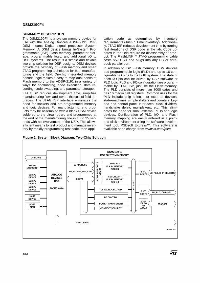
Figure 2. System Block Diagram, Two-Chip Solution
AD
DR
& D
EC
OD
EL
OG
IC
PRIMARYFLASH MEMORY
256K X 8
16 MACROCELL PLD
I/O CONTROL
POWER MANAGEMENT
CONTENT SECURITY
8 I/OPORTS
8 I/OPORTS
JTAGISP TO
ALLAREAS
I/O B
US
22 ADDRESS
8 DATA
WR, RD, BMS, MSx, IOMSI/O, PLD, CHIP SELECTS
I/O, PLD, CHIP SEL
DSM2190F4DSP SYSTEM MEMORY
ANALOGDEVICES
DSP
ADSP-2191
SERIALDEVICE
16 FLAGS
SERIALDEVICE
SERIALDEVICE
UARTDEVICE
JTAG ISP
JTAG DEBUG
HOSTMCU
TIMER/CAPTURE
SECONDARYFLASH MEMORY
32K X 8
AI04959B
5/61
DSM2190F4
The two-chip combination of a DSP and a DSMdevice is ideal for systems which have limitationson size, EMI levels, and power consumption. DSMmemory and logic are “zero-power”, meaning theyautomatically go to standby between memory ac-cesses or logic input changes, producing low ac-tive and standby current consumption, which isideal for battery powered products.
A programmable security bit in the DSM protectsits contents from unauthorized viewing and copy-ing. When set, the security bit will block access ofprogramming devices (JTAG or others) to theDSM Flash memories and PLD configuration. Theonly way to defeat the security bit is to erase theentire DSM device, after which the device is blankand may be used again. The DSP will always haveaccess to Flash memory contents through the 8-bitdata port even while the security bit is set.
Table 1. DSM2190F4V DSP Memory System Devices
Table 2. Compatible Analog Devices DSP
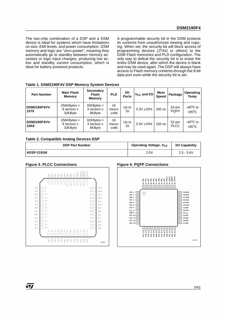
Figure 3. PLCC Connections Figure 4. PQFP Connections
Part Number Main Flash Memory
Secondary Flash
MemoryPLD I/O
PortsVCC and I/O Mem
Speed Package Operating Temp
DSM2190F4VV-15T6
256KBytes =8 sectors x 32KByte
32KBytes =4 sectors x
8KByte
16 macro -cells
Up to 16
3.3V ±10% 150 ns52-pinPQFP
–40oC to
+85oC
DSM2190F4VV-15K6
256KBytes =8 sectors x 32KByte
32KBytes =4 sectors x
8KByte
16 macro -cells
Up to 16
3.3V ±10% 150 ns52-pinPLCC
–40oC to +85oC
DSP Part Number Operating Voltage, VCC I/O Capability
ADSP-2191M 2.5V 2.5 - 3.6V
PB0
PB1
PB2
PB3
PB4
PB5
GND
PB6
PB7
CNTL1
CNTL2
RESET
CNTL0
PA7
PA6
PA5
PA4
PA3
GND
PA2
PA1
PA0
AD0
AD1
AD2
AD3
AD15
AD14
AD13
AD12
AD11
AD10
AD9
AD8
VCC
AD7
AD6
AD5
AD4
PD2
PD1
PD0
PC7
PC6
PC5
PC4
VCC
GND
PC3
PC2
PC1
PC0
8
9
10
11
12
13
14
15
16
17
18
19
20
46
45
44
43
42
41
40
39
38
37
36
35
34
21
22
23
24
25
26
27
28
29
30
31
32
33
47
48
49
50
51
52
1
234567
AI02857
39 AD15
38 AD14
37 AD13
36 AD12
35 AD11
34 AD10
33 AD9
32 AD8
31 VCC
30 AD7
29 AD6
28 AD5
27 AD4
PD2
PD1
PD0
PC7
PC6
PC5
PC4
VCC
GND
PC3
PC2
PC1
PC0
1
2
3
4
5
6
7
8
9
10
11
12
13
52 51 50 49 48 47 46 45 44 43 42 41 40
PB
0
PB
1
PB
2
PB
3
PB
4
PB
5
GN
D
PB
6
PB
7
CN
TL1
CN
TL2
RE
SE
T
CN
TLO
14 15 16 17 18 19 20 21 22 23 24 25 26
PA
7
PA
6
PA
5
PA
4
PA
3
GN
D
PA
2
PA
1
PA
0
AD
0
AD
1
AD
2
AD
3
AI02858
DSM2190F4
6/61
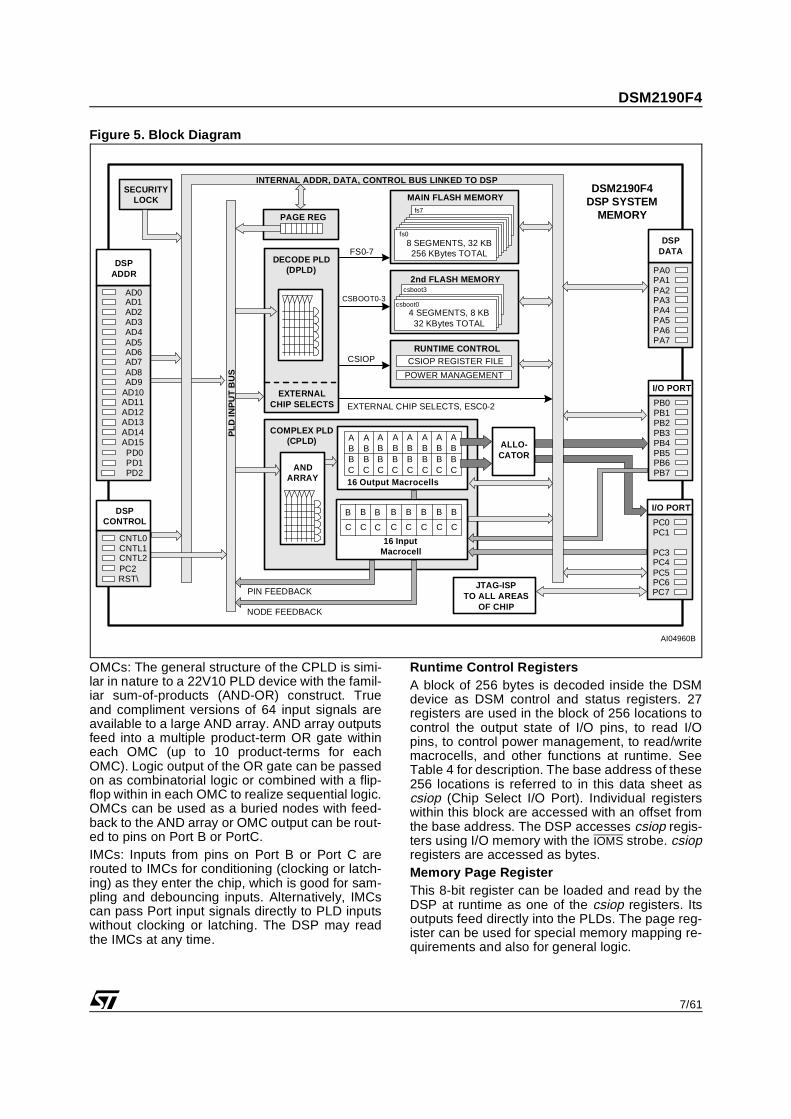
ARCHITECTURAL OVERVIEW Major functional blocks are shown in Figure 5. DSP Address/Data/Control InterfaceThese DSP signals attach directly to the DSM fora glueless connection. An 8-bit data connection isformed and all 22 DSP address lines can be de-coded as well as DSP memory strobes; BMS,IOMS, and MSx. There are many different ways theDSM2190F4 can be configured and used depend-ing on system requirements. One convenient wayis to combine the function of the MSx signals intothe BMS signal. Doing this allows the DSP core toaccess DSM memory at runtime even after theboot process is complete using only the BMS sig-nal. Combining MSx and BMS consumes less I/Opin(s) on the DMS device. See Analog DevicesADSP-2191 DSP Hardware Reference Manual,Chapter 7, Code Example: BMS Runtime Access.Alternatively, any of the MSx signals may also beused to decode any of the sectors of DSM MainFlash or Secondary flash memories.Main Flash MemoryThe 2M bit (256K x 8) Flash memory is divided intoeight equally-sized 32K byte sectors that are indi-vidually selectable through the Decode PLD. EachFlash memory sector can be located at any ad-dress as defined by the user with PSDsoft Ex-press. DSP code and data is easily placed in flashmemory using the PSDsoft Express software de-velopment tool.Secondary Flash MemoryThe 256K bit (32K x 8) Flash memory is dividedinto eight equally-sized 8K byte sectors that are in-dividually selectable through the Decode PLD.Each Flash memory sector can be located at anyaddress as defined by the user with PSDsoft Ex-press. DSP code and data can also be placedSecondary Flash memory using the PSDsoft Ex-press development tool.Secondary flash memory is good for storing databecause of its small sectors. Additionally, softwareEEPROM emulation techniques can be used forsmall data sets that change frequently on a byte-by-byte basis.Secondary flash may also be used to store customstart-up code for applications that do not “boot” us-ing DMA, but instead start executing code from ex-ternal memory upon reset. Storing code here cankeep the entire Main Flash free of initializationcode for clean software partitioning. If only one ormore 8K byte sectors are needed for start-upcode, the remaining sectors of Secondary Flashmay be used for data storage.
Secondary Flash may also be used as an exten-sion to Main Flash memory producing a total of288K bytesMiscellaneous: Main and Secondary Flash memo-ries are totally independent, allowing concurrentoperation if needed. The DSP can read from onememory while erasing or programming the other.The DSP can erase Flash memories by individualsectors or the entire Flash memory array may beerased at one time. Each sector in either Flashmemory may be individually write protected, block-ing any writes from the DSP (good for boot andstart-up code protection). The Flash memories au-tomatically go to standby between DSP read orwrite accesses to conserve power. Maximum ac-cess times include sector decoding time. Maxi-mum erase cycles is 100K and data retention is 15years minimum. Flash memory, as well as the en-tire DSM device may be programmed with theJTAG ISP interface with no DSP involvement.Programmable Logic (PLDs) The DSM family contains two PLDS that may op-tionally run in Turbo or Non-Turbo mode. PLDs op-erate faster (less propagation delay) while inTurbo mode but consume more power than Non-Turbo mode. Non-Turbo mode allows the PLDs toautomatically go to standby when no inputs arechange to conserve power. The Turbo mode set-ting is controlled at runtime by DSP software.Decode PLD (DPLD). This is programmable log-ic used to select one of the eight individual MainFlash memory segments, one of four individualSecondary Flash memory segments, or the groupof control registers within the DSM device. TheDPLD can also optionally drive external chip selectsignals on Port D pins. DPLD input signals include:DSP address and control signals, Page Registeroutputs, DSM Port Pins, CPLD logic feedback. Complex PLD (CPLD). This programmable logicis used to create both combinatorial and sequen-tial general purpose logic. The CPLD contains 16Output Macrocells (OMCs) and 16 Input Macro-cells (IMCs). PSD Macrocell registers are uniquein that that have direct connection to the DSP databus allowing them to be loaded and read directlyby the DSP at runtime. This direct access is goodfor making small peripheral devices (shifters,counters, state machines, etc.) that are accesseddirectly by the DSP with little overhead. DPLD in-puts include DSP address and control signals,Page Register outputs, DSM Port Pins, and CPLDfeedback.
7/61
DSM2190F4
Figure 5. Block Diagram
OMCs: The general structure of the CPLD is simi-lar in nature to a 22V10 PLD device with the famil-iar sum-of-products (AND-OR) construct. Trueand compliment versions of 64 input signals areavailable to a large AND array. AND array outputsfeed into a multiple product-term OR gate withineach OMC (up to 10 product-terms for eachOMC). Logic output of the OR gate can be passedon as combinatorial logic or combined with a flip-flop within in each OMC to realize sequential logic.OMCs can be used as a buried nodes with feed-back to the AND array or OMC output can be rout-ed to pins on Port B or PortC. IMCs: Inputs from pins on Port B or Port C arerouted to IMCs for conditioning (clocking or latch-ing) as they enter the chip, which is good for sam-pling and debouncing inputs. Alternatively, IMCscan pass Port input signals directly to PLD inputswithout clocking or latching. The DSP may readthe IMCs at any time.
Runtime Control RegistersA block of 256 bytes is decoded inside the DSMdevice as DSM control and status registers. 27registers are used in the block of 256 locations tocontrol the output state of I/O pins, to read I/Opins, to control power management, to read/writemacrocells, and other functions at runtime. SeeTable 4 for description. The base address of these256 locations is referred to in this data sheet ascsiop (Chip Select I/O Port). Individual registerswithin this block are accessed with an offset fromthe base address. The DSP accesses csiop regis-ters using I/O memory with the IOMS strobe. csiopregisters are accessed as bytes.Memory Page RegisterThis 8-bit register can be loaded and read by theDSP at runtime as one of the csiop registers. Itsoutputs feed directly into the PLDs. The page reg-ister can be used for special memory mapping re-quirements and also for general logic.
PB0PB1PB2PB3PB4PB5PB6PB7
I/O PORT
PC0PC1
PC3PC4PC5PC6
I/O PORT
COMPLEX PLD(CPLD)
16 InputMacrocell
16 Output Macrocells
AB
AB
AB
AB
AB
AB
AB
AB
BC
BC
BC
BC
BC
BC
BC
BC
PAGE REG
SECURITYLOCK
PLD
INP
UT
BU
S
ALLO-CATOR
PIN FEEDBACK
NODE FEEDBACK
DSM2190F4DSP SYSTEM
MEMORY
INTERNAL ADDR, DATA, CONTROL BUS LINKED TO DSP
DECODE PLD(DPLD)
ANDARRAY
EXTERNALCHIP SELECTS
JTAG-ISPTO ALL AREAS
OF CHIP
B B B B
C C C C
B
C
B
C
B
C
B
C
EXTERNAL CHIP SELECTS, ESC0-2
RUNTIME CONTROLCSIOP REGISTER FILE
POWER MANAGEMENT
CSIOP
MAIN FLASH MEMORY
8 SEGMENTS, 32 KB256 KBytes TOTAL
fs0
fs7
2nd FLASH MEMORY
4 SEGMENTS, 8 KB32 KBytes TOTAL
csboot0
csboot3CSBOOT0-3
FS0-7
AD0
DSPADDR
AD1AD2AD3AD4AD5AD6AD7AD8AD9
AD10AD11AD12AD13AD14AD15PD0PD1PD2
PC7
DSPCONTROL
CNTL0CNTL1CNTL2
RST\
PA0PA1PA2PA3PA4PA5PA6PA7
DSPDATA
PC2
AI04960B
DSM2190F4
8/61
I/O PortsThe DSM has 19 individually configurable I/O pinsdistributed over the three ports (Ports B, C, and D).Each I/O pin can be individually configured for dif-ferent functions such as standard MCU I/O portsor PLD I/O on a pin by pin basis. (MCU I/O meansthat for each pin, its output state can be controlledor its input value can be read by the DSP at runt-ime using the csiop registers like an MCU woulddo.)Port C hosts the JTAG ISP signals. Since JTAG-ISP does not occur frequently during the life of aproduct, those Port C pins are under-utilized. Inapplications that need every I/O pin, JTAG signalscan be multiplexed with general I/O signals to usethem for I/O when not performing ISP. See sectiontitled “Programming In-Circuit using JTAG ISP” onpage 40 for muxing JTAG pins on Port C, and Ap-plication Note AN1153. The static configuration of all Port pins is definedwith the PSDsoft ExpressTM software develop-ment tool. The dynamic action of the Ports pins iscontrolled by DSP runtime software. JTAG ISP PortIn-System Programming (ISP) can be performedthrough the JTAG signals on Port C. This serial in-terface allows programming of the entire DSM de-vice or subsections (that is, only Flash memory butnot the PLDs) without the participation of the DSP.A blank DSM device soldered to a circuit boardcan be completely programmed in 10 to 25 sec-onds. The basic JTAG signals; TMS, TCK, TDI,and TDO form the IEEE-1149.1 interface. TheDSM device does not implement the IEEE-1149.1Boundary Scan functions. The DSM uses theJTAG interface for ISP only. However, the DSMdevice can reside in a standard JTAG chain withother JTAG devices (including the ADSP-2191)and it will remain in BYPASS mode while other de-vices perform Boundary Scan. ISP programming time can be reduced as much as30% by using two more signals on Port C, TSTATand TERR in addition to TMS, TCK, TDI and TDO.
The FlashLINKTM JTAG programming cable isavailable from STMicroelectronics for $59USDand PSDsoft Express software is available at nocharge from www.st.com/psm. That is all that isneeded to program a DSM device using the paral-lel port on any PC or note-book. See section titled“Programming In-Circuit using JTAG ISP” on page40.Power Management The DSM has bits in csiop control registers thatare configured at run-time by the DSP to reducepower consumption of the CPLD. The Turbo bit inthe PMMR0 register can be set to logic 1 and theCPLD will go to Non-Turbo mode, meaning it willlatch its outputs and go to sleep until the next tran-sition on its inputs. There is a slight penalty in PLDperformance (longer propagation delay), but sig-nificant power savings are realized.Additionally, bits in two csiop registers can be setby the DSP to selectively block signals from enter-ing the CPLD which reduces power consumption.See section titled “Power Management” on page37.Security and NVM Sector ProtectionA programmable security bit in the DSM protectsits contents from unauthorized viewing and copy-ing. When set, the security bit will block access ofprogramming devices (JTAG or others) to theDSM Flash memory and PLD configuration. Theonly way to defeat the security bit is to erase theentire DSM device, after which the device is blankand may be used again. Additionally, the contents of each individual Flashmemory sector can be write protected (sector pro-tection) by configuration with PSDsoft ExpressTM.This is typically used to protect DSP boot codefrom being corrupted by inadvertent writes toFlash memory from the DSP. Pin AssignmentsPin assignment are shown for the 52-pin PLCCpackage in Figure 3, and the 52-pin PQFP pack-age in Figure 4.
9/61
DSM2190F4
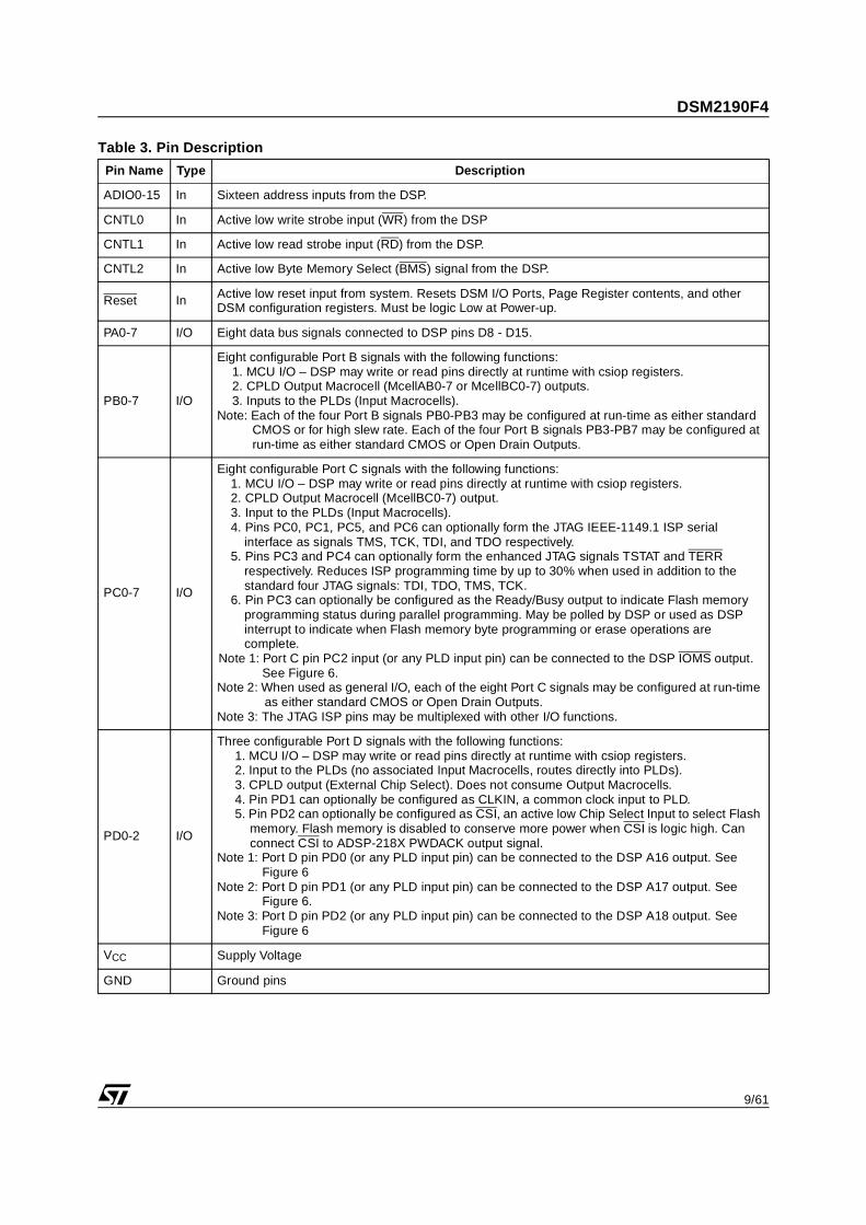
Table 3. Pin Description
Pin Name Type Description
ADIO0-15 In Sixteen address inputs from the DSP.
CNTL0 In Active low write strobe input (WR) from the DSP
CNTL1 In Active low read strobe input (RD) from the DSP.
CNTL2 In Active low Byte Memory Select (BMS) signal from the DSP.
Reset In Active low reset input from system. Resets DSM I/O Ports, Page Register contents, and other DSM configuration registers. Must be logic Low at Power-up.
PA0-7 I/O Eight data bus signals connected to DSP pins D8 - D15.
PB0-7 I/O
Eight configurable Port B signals with the following functions:1. MCU I/O – DSP may write or read pins directly at runtime with csiop registers.2. CPLD Output Macrocell (McellAB0-7 or McellBC0-7) outputs.3. Inputs to the PLDs (Input Macrocells).
Note: Each of the four Port B signals PB0-PB3 may be configured at run-time as either standard CMOS or for high slew rate. Each of the four Port B signals PB3-PB7 may be configured at run-time as either standard CMOS or Open Drain Outputs.
PC0-7 I/O
Eight configurable Port C signals with the following functions:1. MCU I/O – DSP may write or read pins directly at runtime with csiop registers.2. CPLD Output Macrocell (McellBC0-7) output.3. Input to the PLDs (Input Macrocells).4. Pins PC0, PC1, PC5, and PC6 can optionally form the JTAG IEEE-1149.1 ISP serial
interface as signals TMS, TCK, TDI, and TDO respectively.5. Pins PC3 and PC4 can optionally form the enhanced JTAG signals TSTAT and TERR
respectively. Reduces ISP programming time by up to 30% when used in addition to the standard four JTAG signals: TDI, TDO, TMS, TCK.
6. Pin PC3 can optionally be configured as the Ready/Busy output to indicate Flash memory programming status during parallel programming. May be polled by DSP or used as DSP interrupt to indicate when Flash memory byte programming or erase operations are complete.
Note 1: Port C pin PC2 input (or any PLD input pin) can be connected to the DSP IOMS output. See Figure 6.
Note 2: When used as general I/O, each of the eight Port C signals may be configured at run-time as either standard CMOS or Open Drain Outputs.
Note 3: The JTAG ISP pins may be multiplexed with other I/O functions.
PD0-2 I/O
Three configurable Port D signals with the following functions:1. MCU I/O – DSP may write or read pins directly at runtime with csiop registers.2. Input to the PLDs (no associated Input Macrocells, routes directly into PLDs).3. CPLD output (External Chip Select). Does not consume Output Macrocells.4. Pin PD1 can optionally be configured as CLKIN, a common clock input to PLD.5. Pin PD2 can optionally be configured as CSI, an active low Chip Select Input to select Flash
memory. Flash memory is disabled to conserve more power when CSI is logic high. Can connect CSI to ADSP-218X PWDACK output signal.
Note 1: Port D pin PD0 (or any PLD input pin) can be connected to the DSP A16 output. See Figure 6
Note 2: Port D pin PD1 (or any PLD input pin) can be connected to the DSP A17 output. See Figure 6.
Note 3: Port D pin PD2 (or any PLD input pin) can be connected to the DSP A18 output. See Figure 6
VCC Supply Voltage
GND Ground pins
DSM2190F4
10/61
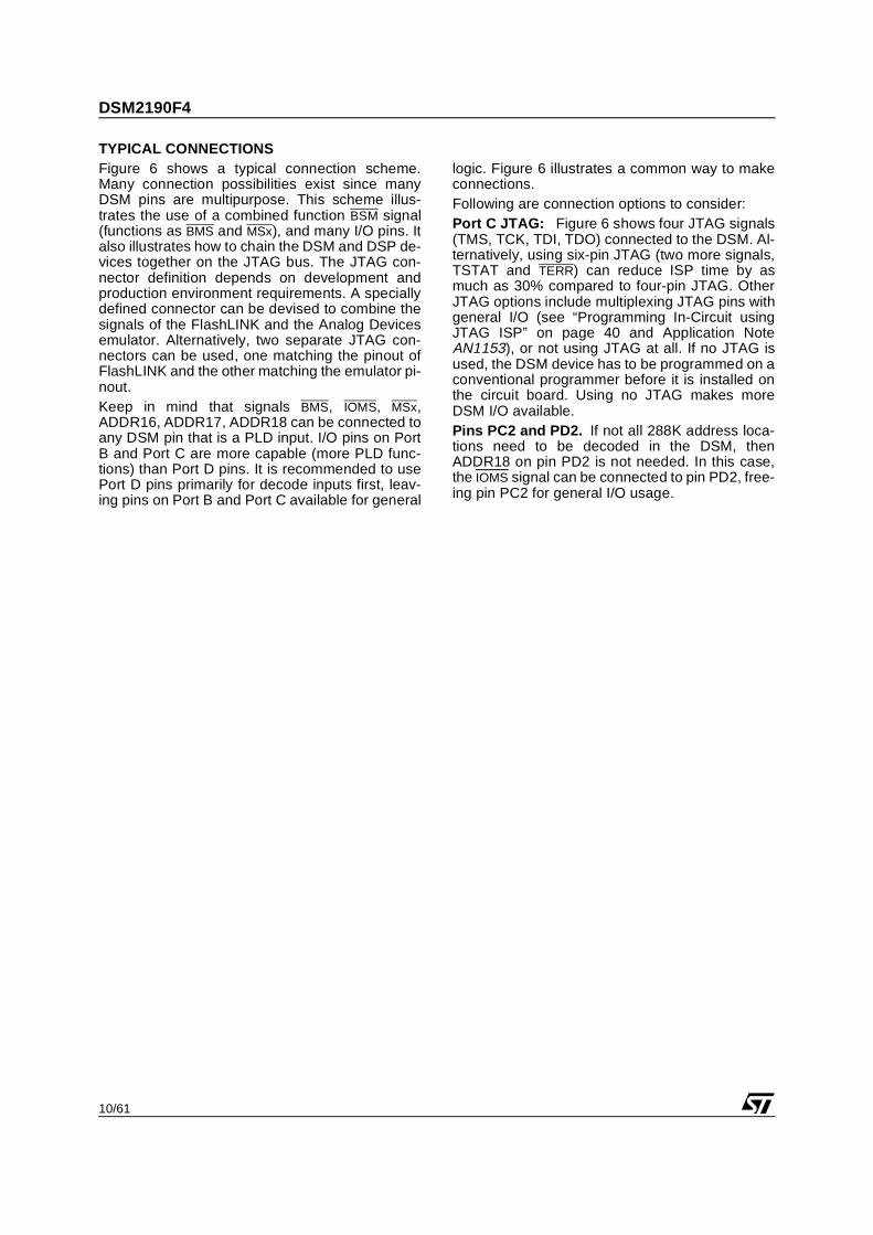
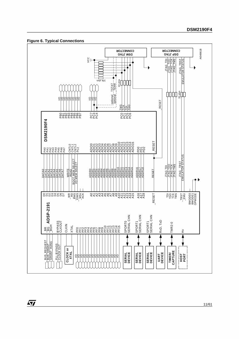
TYPICAL CONNECTIONSFigure 6 shows a typical connection scheme.Many connection possibilities exist since manyDSM pins are multipurpose. This scheme illus-trates the use of a combined function BSM signal(functions as BMS and MSx), and many I/O pins. Italso illustrates how to chain the DSM and DSP de-vices together on the JTAG bus. The JTAG con-nector definition depends on development andproduction environment requirements. A speciallydefined connector can be devised to combine thesignals of the FlashLINK and the Analog Devicesemulator. Alternatively, two separate JTAG con-nectors can be used, one matching the pinout ofFlashLINK and the other matching the emulator pi-nout.Keep in mind that signals BMS, IOMS, MSx,ADDR16, ADDR17, ADDR18 can be connected toany DSM pin that is a PLD input. I/O pins on PortB and Port C are more capable (more PLD func-tions) than Port D pins. It is recommended to usePort D pins primarily for decode inputs first, leav-ing pins on Port B and Port C available for general
logic. Figure 6 illustrates a common way to makeconnections.Following are connection options to consider: Port C JTAG: Figure 6 shows four JTAG signals(TMS, TCK, TDI, TDO) connected to the DSM. Al-ternatively, using six-pin JTAG (two more signals,TSTAT and TERR) can reduce ISP time by asmuch as 30% compared to four-pin JTAG. OtherJTAG options include multiplexing JTAG pins withgeneral I/O (see “Programming In-Circuit usingJTAG ISP” on page 40 and Application NoteAN1153), or not using JTAG at all. If no JTAG isused, the DSM device has to be programmed on aconventional programmer before it is installed onthe circuit board. Using no JTAG makes moreDSM I/O available.Pins PC2 and PD2. If not all 288K address loca-tions need to be decoded in the DSM, thenADDR18 on pin PD2 is not needed. In this case,the IOMS signal can be connected to pin PD2, free-ing pin PC2 for general I/O usage.
11/61
DSM2190F4
Figure 6. Typical Connections
JTA
G_T
RS
TE
MU
LAT
OR
ST
AT
US
AD
SP
-219
1
A0
A1
A2
A3
A4
A5
A6
A7
A8
A9
A10
A11
CLK
IN
XT
AL
AD
DR
0A
DD
R1
AD
DR
2A
DD
R3
AD
DR
4A
DD
R5
AD
DR
6A
DD
R7
AD
DR
8A
DD
R9
AD
DR
10A
DD
R11
A12
A13
A14
A15
AD
DR
12A
DD
R13
AD
DR
14A
DD
R15
A18
AD
DR
16
_RE
SE
T
SP
OR
T0
SE
RIA
L C
HN
SE
RIA
LD
EV
ICE
SP
OR
T1
SE
RIA
L C
HN
SE
RIA
LD
EV
ICE
PF
0P
F1
PF
2
PF
8P
F9
PF
6
PF
10
PF
7
PF
3P
F4
PF
5
I/O
CLO
CK
or
XT
AL
_BR
_BG
_BG
H
BU
S_R
EQ
UE
ST
GR
AN
T_H
UN
GB
US
_GR
AN
T
CLO
CK
OU
TC
LKO
UT
I/OI/OI/OI/OI/O I/O
DA
TA
0D
AT
A1
DA
TA
2D
AT
A3
DA
TA
4D
AT
A5
DA
TA
6D
AT
A7
D0
D1
D2
D3
D4
D5
D6
D7
BO
OT
ME
M S
ELE
CT
_RD
_BM
S_I
OM
S_M
Sx
_WR
WR
ITE
RE
AD
I/O I/OI/OI/OI/OP
F11
PF
12P
F13
PF
14P
F15
I/OI/OI/O I/O
SP
OR
T1
SE
RIA
L C
HN
SE
RIA
LD
EV
ICE
RxD
, TxD
UA
RT
DE
VIC
E
TIM
ER
/C
AP
TU
RE
AD
IO0
AD
IO1
AD
IO2
AD
IO3
AD
IO4
AD
IO5
AD
IO6
AD
IO7
AD
IO8
AD
IO9
AD
IO10
AD
IO11
PC
7
PC
1P
C0
PC
6P
C5
AD
IO12
AD
IO13
AD
IO14
AD
IO15
PD
1P
D2
PD
0
_RE
SE
T
DSM JTAGCONNECTOR
TM
ST
CK
TD
IT
DO
_RE
SE
T
VC
C
DS
M21
90F
4P
A0
PA
1P
A2
PA
3P
A4
PA
5P
A6
PA
7
CN
TL0
CN
TL1
CN
TL2
AD
DR
17A
16A
17A
DD
R18
RE
SE
T
PC
3I/O
PC
4I/O
PC
2
I/O
I/O M
EM
SE
LEC
T
AC
K
HO
ST
PO
RT
Hx
TM
R2-
0
BM
OD
E0
BM
OD
E1
OP
MO
DE
PLL
BY
PA
SS
BY
PA
SS
TD
OT
DI
TC
KT
MS
_TR
ST
_EM
U
optio
nal
TS
TA
Top
tiona
l _
TE
RR
PB
3P
B2
PB
1P
B0
PB
7P
B6
PB
5P
B4
I/OI/OI/OI/OI/OI/OI/OI/O
JTA
G T
MS
JTA
G T
CK
JTA
G T
DI
JTA
G T
DO
JTA
G _
TR
ST
EM
ULA
TO
R S
TA
TU
S
AI0
4961
B
DSP JTAGCONNECTOR
JTA
G_
TC
KJT
AG
_TM
S
JTA
G_T
DI
JTA
G_
TD
O
10k ohm
33 o
hm
33 o
hm

DSM2190F4
12/61
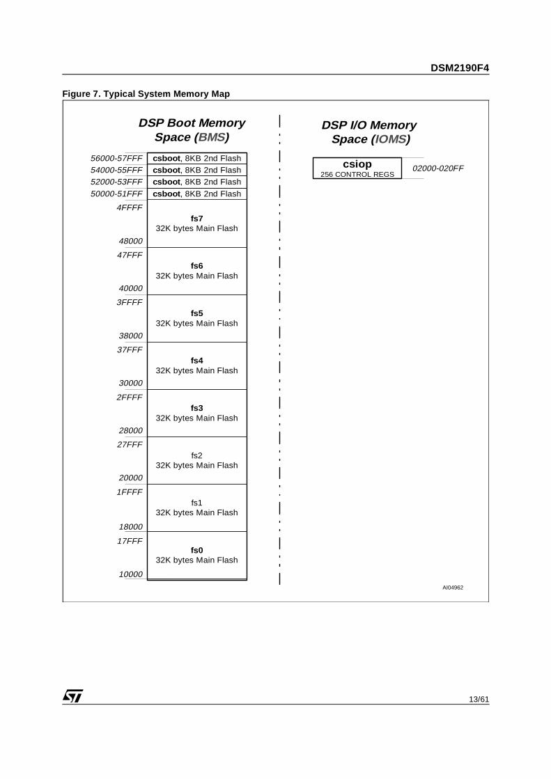
TYPICAL MEMORY MAPThere many different ways to place (or map) theaddresses of DSM memory and I/O depending onsystem requirements. The DPLD allows completemapping flexibility. Figure 7 shows one possiblesystem memory map. In this case, the DSP willbootload (via DMA) the contents of Main Flashmemory upon reset. The Secondary Flash memo-ry can be used for parameter storage or additionalcode storage. BMS and MSx are configured in theDSP to be combined into the BMS signal, allowingthe DSP to access both Flash memories at runt-ime (after DMA boot). The DSP may execute code
directly from the DSM and well as erase and writenew code or data to DSM Flash. The nomenclature fs0..fs7 are designators for theindividual sectors of Main Flash memory, 32Kbytes each. csboot0..csboot3 are designators forthe individual Secondary Flash memory seg-ments, 8K bytes each. csiop designates the DSMcontrol register block. The designer may easily specify memory mappingin a point-and-click software environment usingPSDsoft ExpressTM.
13/61
DSM2190F4
Figure 7. Typical System Memory Map
DSP Boot MemorySpace (BMS)
DSP I/O Memory Space ( IOMS)
csiop256 CONTROL REGS
18000
1FFFF
20000
27FFF
2FFFF
37FFF
3FFFF
47FFF
4FFFF
28000
30000
38000
40000
48000
17FFF
10000
fs032K bytes Main Flash
fs132K bytes Main Flash
fs732K bytes Main Flash
fs632K bytes Main Flash
fs532K bytes Main Flash
fs432K bytes Main Flash
fs332K bytes Main Flash
fs232K bytes Main Flash
csboot , 8KB 2nd Flash
csboot , 8KB 2nd Flashcsboot , 8KB 2nd Flashcsboot , 8KB 2nd Flash
50000-51FFF52000-53FFF54000-55FFF56000-57FFF
02000-020FF
AI04962
DSM2190F4
14/61
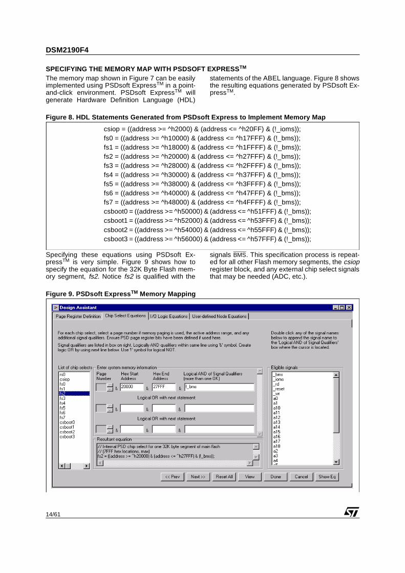
SPECIFYING THE MEMORY MAP WITH PSDSOFT EXPRESSTM
The memory map shown in Figure 7 can be easilyimplemented using PSDsoft ExpressTM in a point-and-click environment. PSDsoft ExpressTM willgenerate Hardware Definition Language (HDL)
statements of the ABEL language. Figure 8 showsthe resulting equations generated by PSDsoft Ex-pressTM.
Figure 8. HDL Statements Generated from PSDsoft Express to Implement Memory Map
Specifying these equations using PSDsoft Ex-pressTM is very simple. Figure 9 shows how tospecify the equation for the 32K Byte Flash mem-ory segment, fs2. Notice fs2 is qualified with the
signals BMS. This specification process is repeat-ed for all other Flash memory segments, the csiopregister block, and any external chip select signalsthat may be needed (ADC, etc.).
Figure 9. PSDsoft ExpressTM Memory Mapping
csiop = ((address >= ^h2000) & (address <= ^h20FF) & (!_ioms));fs0 = ((address >= ^h10000) & (address <= ^h17FFF) & (!_bms));fs1 = ((address >= ^h18000) & (address <= ^h1FFFF) & (!_bms));fs2 = ((address >= ^h20000) & (address <= ^h27FFF) & (!_bms));fs3 = ((address >= ^h28000) & (address <= ^h2FFFF) & (!_bms));fs4 = ((address >= ^h30000) & (address <= ^h37FFF) & (!_bms));fs5 = ((address >= ^h38000) & (address <= ^h3FFFF) & (!_bms));fs6 = ((address >= ^h40000) & (address <= ^h47FFF) & (!_bms));fs7 = ((address >= ^h48000) & (address <= ^h4FFFF) & (!_bms));csboot0 = ((address >= h50000) & (address <= h51FFF) & (!_bms));csboot1 = ((address >= h52000) & (address <= h53FFF) & (!_bms));csboot2 = ((address >= h54000) & (address <= h55FFF) & (!_bms));csboot3 = ((address >= h56000) & (address <= h57FFF) & (!_bms));
15/61
DSM2190F4
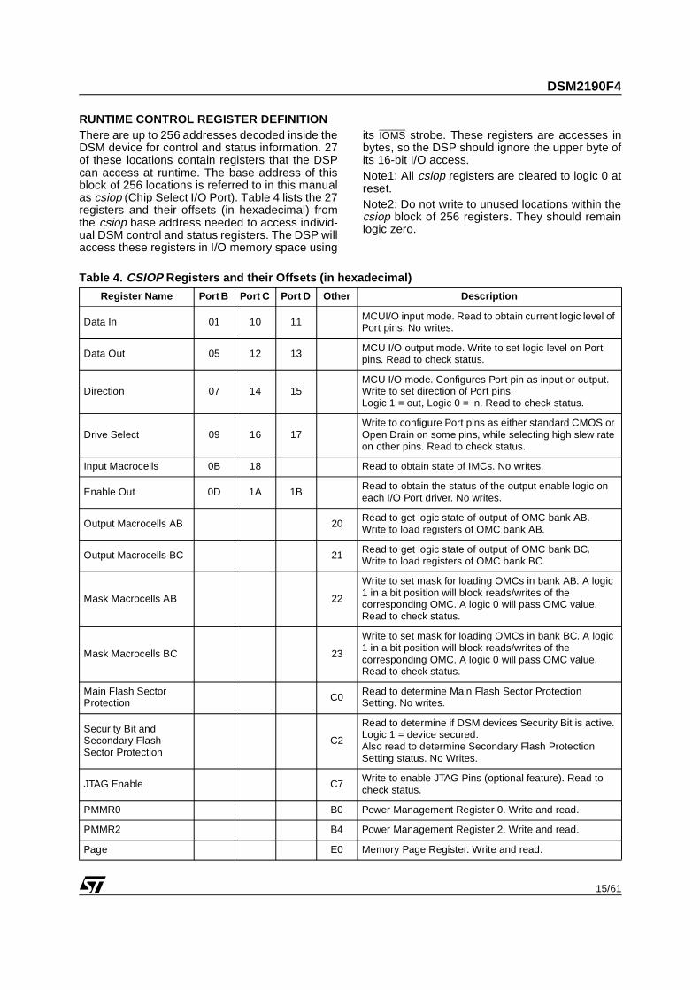
RUNTIME CONTROL REGISTER DEFINITIONThere are up to 256 addresses decoded inside theDSM device for control and status information. 27of these locations contain registers that the DSPcan access at runtime. The base address of thisblock of 256 locations is referred to in this manualas csiop (Chip Select I/O Port). Table 4 lists the 27registers and their offsets (in hexadecimal) fromthe csiop base address needed to access individ-ual DSM control and status registers. The DSP willaccess these registers in I/O memory space using
its IOMS strobe. These registers are accesses inbytes, so the DSP should ignore the upper byte ofits 16-bit I/O access. Note1: All csiop registers are cleared to logic 0 atreset.Note2: Do not write to unused locations within thecsiop block of 256 registers. They should remainlogic zero.
Table 4. CSIOP Registers and their Offsets (in hexadecimal)
Register Name Port B Port C Port D Other Description
Data In 01 10 11 MCUI/O input mode. Read to obtain current logic level of Port pins. No writes.
Data Out 05 12 13 MCU I/O output mode. Write to set logic level on Port pins. Read to check status.
Direction 07 14 15 MCU I/O mode. Configures Port pin as input or output. Write to set direction of Port pins. Logic 1 = out, Logic 0 = in. Read to check status.
Drive Select 09 16 17 Write to configure Port pins as either standard CMOS or Open Drain on some pins, while selecting high slew rate on other pins. Read to check status.
Input Macrocells 0B 18 Read to obtain state of IMCs. No writes.
Enable Out 0D 1A 1B Read to obtain the status of the output enable logic on each I/O Port driver. No writes.
Output Macrocells AB 20Read to get logic state of output of OMC bank AB.Write to load registers of OMC bank AB.
Output Macrocells BC 21Read to get logic state of output of OMC bank BC.Write to load registers of OMC bank BC.
Mask Macrocells AB 22
Write to set mask for loading OMCs in bank AB. A logic 1 in a bit position will block reads/writes of the corresponding OMC. A logic 0 will pass OMC value. Read to check status.
Mask Macrocells BC 23
Write to set mask for loading OMCs in bank BC. A logic 1 in a bit position will block reads/writes of the corresponding OMC. A logic 0 will pass OMC value. Read to check status.
Main Flash Sector Protection C0
Read to determine Main Flash Sector Protection Setting. No writes.
Security Bit and Secondary Flash Sector Protection
C2
Read to determine if DSM devices Security Bit is active. Logic 1 = device secured. Also read to determine Secondary Flash Protection Setting status. No Writes.
JTAG Enable C7 Write to enable JTAG Pins (optional feature). Read to check status.
PMMR0 B0 Power Management Register 0. Write and read.
PMMR2 B4 Power Management Register 2. Write and read.
Page E0 Memory Page Register. Write and read.
DSM2190F4
16/61
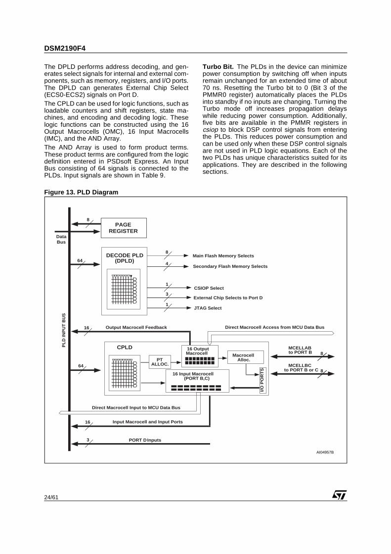
DETAILED OPERATIONFigure 5 shows major functional areas of the de-vice: Flash Memories
PLDs (DPLD, CPLD, Page Register)
DSP Bus Interface (Address, Data, Control)
I/O Ports
Runtime Control Registers
JTAG ISP Interface
The following describes these functions in moredetail. Flash MemoriesThe Main Flash memory array is divided into eightequal 32K byte sectors. The Secondary Flashmemory array is divided into four equal 8K bytesectors. Each sector is selected by the DPLD canbe separately protected from program and erasecycles. This configuration is specified by using PS-Dsoft ExpressTM.Memory Sector Select Signals. The DPLD gen-erates the Select signals for all the internal memo-ry blocks (see Figure 14). Each of the twelvesectors of the Flash memories has a select signal(FS0-FS7, or CSBOOT0-CSBOOT3) which con-tains up to three product terms. Having three prod-uct terms for each select signal allows a givensector to be mapped into multiple areas of systemmemory if needed.Ready/Busy (PC3). This signal can be used tooutput the Ready/Busy status of the device. Theoutput on Ready/Busy is a 0 (Busy) when eitherFlash memory array is being written, or when ei-ther Flash memory array is being erased. The out-put is a 1 (Ready) when no Write or Erase cycle is
in progress. This signal may be polled by the DSPor used as a DSP interrupt to indicate when anerase or program cycle is complete.Memory Operation. The Flash memories are ac-cessed through the DSP Address, Data, and Con-trol Bus Interface. DSPs and MCUs cannot write to Flash memory asit would an SRAM device. Flash memory must firstbe “unlocked” with a special sequence of bytewrite operations to invoke an internal algorithm,then a single data byte is written to the Flash mem-ory array, then programming status is checked bya byte read operation or by checking the Ready/Busy pin (PC3). Table 5 lists all of the special in-struction sequences to program (write) data to theFlash memory arrays, erase the arrays, and checkfor different types of status from the arrays. Theseinstruction sequences are different combinationsof individual byte write and byte read operations.IMPORTANT: The DSP may not read and executecode from the same Flash memory array for whichit is directing an instruction sequence. Or moresimply stated, the DSP may not read code thesame Flash array that is writing or erasing. In-stead, the DSP must execute code from an alter-nate memory (like its own internal SRAM or adifferent Flash array) while sending instructions toa given Flash array. Since the two Flash memoryarrays inside the DSM device are completely inde-pendent, the DSP may read code from one arraywhile sending instructions to the other.After a Flash memory array is programmed (writ-ten) it will go to “Read Array” mode, then the DSPcan read from Flash memory just as if would fromany 8-bit ROM or SRAM device.
17/61
DSM2190F4
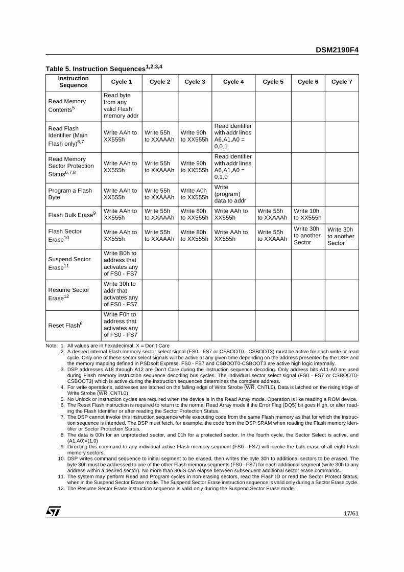
Table 5. Instruction Sequences1,2,3,4
Note: 1. All values are in hexadecimal, X = Don’t Care2. A desired internal Flash memory sector select signal (FS0 - FS7 or CSBOOT0 - CSBOOT3) must be active for each write or read
cycle. Only one of these sector select signals will be active at any given time depending on the address presented by the DSP andthe memory mapping defined in PSDsoft Express. FS0 - FS7 and CSBOOT0-CSBOOT3 are active high logic internally.
3. DSP addresses A18 through A12 are Don’t Care during the instruction sequence decoding. Only address bits A11-A0 are usedduring Flash memory instruction sequence decoding bus cycles. The individual sector select signal (FS0 - FS7 or CSBOOT0-CSBOOT3) which is active during the instruction sequences determines the complete address.
4. For write operations, addresses are latched on the falling edge of Write Strobe (WR, CNTL0), Data is latched on the rising edge ofWrite Strobe (WR, CNTL0)
5. No Unlock or Instruction cycles are required when the device is in the Read Array mode. Operation is like reading a ROM device.6. The Reset Flash instruction is required to return to the normal Read Array mode if the Error Flag (DQ5) bit goes High, or after read-
ing the Flash Identifier or after reading the Sector Protection Status.7. The DSP cannot invoke this instruction sequence while executing code from the same Flash memory as that for which the instruc-
tion sequence is intended. The DSP must fetch, for example, the code from the DSP SRAM when reading the Flash memory Iden-tifier or Sector Protection Status.
8. The data is 00h for an unprotected sector, and 01h for a protected sector. In the fourth cycle, the Sector Select is active, and(A1,A0)=(1,0)
9. Directing this command to any individual active Flash memory segment (FS0 - FS7) will invoke the bulk erase of all eight Flashmemory sectors.
10. DSP writes command sequence to initial segment to be erased, then writes the byte 30h to additional sectors to be erased. Thebyte 30h must be addressed to one of the other Flash memory segments (FS0 - FS7) for each additional segment (write 30h to anyaddress within a desired sector). No more than 80uS can elapse between subsequent additional sector erase commands.
11. The system may perform Read and Program cycles in non-erasing sectors, read the Flash ID or read the Sector Protect Status,when in the Suspend Sector Erase mode. The Suspend Sector Erase instruction sequence is valid only during a Sector Erase cycle.
12. The Resume Sector Erase instruction sequence is valid only during the Suspend Sector Erase mode.
Instruction Sequence Cycle 1 Cycle 2 Cycle 3 Cycle 4 Cycle 5 Cycle 6 Cycle 7
Read Memory
Contents5
Read byte from any valid Flash memory addr
Read Flash Identifier (Main
Flash only)6,7
Write AAh to XX555h
Write 55h to XXAAAh
Write 90h to XX555h
Read identifier with addr lines A6,A1,A0 = 0,0,1
Read Memory Sector Protection Status6,7,8
Write AAh to XX555h
Write 55h to XXAAAh
Write 90h to XX555h
Read identifier with addr lines A6,A1,A0 = 0,1,0
Program a Flash Byte
Write AAh to XX555h
Write 55h to XXAAAh
Write A0h to XX555h
Write (program) data to addr
Flash Bulk Erase9 Write AAh to XX555h
Write 55h to XXAAAh
Write 80h to XX555h
Write AAh to XX555h
Write 55h to XXAAAh
Write 10h to XX555h
Flash Sector Erase10
Write AAh to XX555h
Write 55h to XXAAAh
Write 80h to XX555h
Write AAh to XX555h
Write 55h to XXAAAh
Write 30h to another Sector
Write 30h
to another Sector
Suspend Sector
Erase11
Write B0h to address that activates any of FS0 - FS7
Resume Sector Erase12
Write 30h to addr that activates any of FS0 - FS7
Reset Flash6
Write F0h to address that activates any of FS0 - FS7
DSM2190F4
18/61
Instruction SequencesAn instruction sequence consists of a sequence ofspecific write or read operations. Each byte writtento the device is received and sequentially decodedand not executed as a standard write operation tothe memory array. The instruction sequence is ex-ecuted when the correct number of bytes are prop-erly received and the time between twoconsecutive bytes is shorter than the time-out pe-riod. Some instruction sequences are structured toinclude read operations after the initial write oper-ations.The instruction sequence must be followed exact-ly. Any invalid combination of instruction bytes ortime-out between two consecutive bytes while ad-dressing Flash memory resets the device logic intoRead Array mode (Flash memory is read like aROM device). The device supports the instructionsequences summarized in Table 5:Flash memory: Erase memory by chip or sector
Suspend or resume sector erase
Program a Byte
Reset to Read Array mode
Read primary Flash Identifier value
Read Sector Protection Status
These instruction sequences are detailed in Table5. For efficient decoding of the instruction se-quences, the first two bytes of an instruction se-quence are the coded cycles and are followed byan instruction byte or confirmation byte. The codedcycles consist of writing the data AAh to addressXX555h during the first cycle and data 55h to ad-dress XXAAAh during the second cycle. Addresssignals A18-A12 are Don’t Care during the instruc-tion sequence Write cycles. However, the appro-priate internal Sector Select (FS0-FS7 orCSBOOT0-CSBOOT3) must be selected internal-ly (active, which is logic 1).
Reading Flash MemoryUnder typical conditions, the DSP may read theFlash memory using read operations just as itwould a ROM or RAM device. Alternately, the DSPmay use read operations to obtain status informa-tion about a Program or Erase cycle that is cur-rently in progress. Lastly, the DSP may useinstruction sequences to read special data fromthese memory blocks. The following sections de-scribe these read instruction sequences.Read Memory Contents. Flash memory isplaced in the Read Array mode after Power-up,chip reset, or a Reset Flash memory instructionsequence (see Table 5). The DSP can read thememory contents of the Flash memory by usingread operations any time the read operation is notpart of an instruction sequence.Read Main Flash Identifier. The Main Flashmemory identifier is read with an instruction se-quence composed of 4 operations: 3 specific writeoperations and a read operation (see Table 5).During the read operation, address bits A6, A1,and A0 must be 0,0,1, respectively, and the appro-priate internal Sector Select (FS0-FS7) must beactive. The identifier is 0xE7. Not Applicable toSecondary Flash.Read Memory Sector Protection Status. TheFlash memory Sector Protection Status is readwith an instruction sequence composed of 4 oper-ations: 3 specific write operations and a read oper-ation (see Table 5). During the read operation,address bits A6, A1, and A0 must be 0,1,0, re-spectively, while internal Sector Select (FS0-FS7or CSBOOT0-CSBOOT3) designates the Flashmemory sector whose protection has to be veri-fied. The read operation produces 01h if the Flashmemory sector is protected, or 00h if the sector isnot protected.The sector protection status can also be read bythe DSP accessing the Flash memory Protectionregisters in csiop space. See the section entitled“Flash Memory Sector Protect” for register defini-tions.
Table 6. Status Bit Definition
Note: 1. X = Not guaranteed value, can be read either 1 or 0.2. DQ7-DQ0 represent the Data Bus bits, D7-D0.
Reading the Erase/Program Status Bits. Thedevice provides several status bits to be used bythe DSP to confirm the completion of an Erase or
Program cycle of Flash memory. These status bitsminimize the time that the DSP spends performingthese tasks and are defined in Table 6. The statusbits can be read as many times as needed.
Functional Block FS0-FS7, or CSBOOT0-CSBOOT3 DQ7 DQ6 DQ5 DQ4 DQ3 DQ2 DQ1 DQ0
Flash MemoryActive (the desired
segment is selected)Data
PollingToggle Flag
Error Flag
XErase Time-
outX X X
19/61
DSM2190F4
For Flash memory, the DSP can perform a readoperation to obtain these status bits while anErase or Program instruction sequence is beingexecuted by the embedded algorithm. See thesection entitled “Programming Flash Memory”, onpage 19, for details.Data Polling Flag (DQ7). When erasing or pro-gramming in Flash memory, the Data Polling Flag(DQ7) bit outputs the complement of the bit beingentered for programming/writing on the Data Poll-ing Flag (DQ7) bit. Once the Program instructionsequence or the write operation is completed, thetrue logic value is read on the Data Polling Flag(DQ7) bit (in a read operation). Flash memory instruction features. Data Polling is effective after the fourth Write
pulse (for a Program instruction sequence) or after the sixth Write pulse (for an Erase instruction sequence). It must be performed at the address being programmed or at an address within the Flash memory sector being erased.
During an Erase cycle, the Data Polling Flag (DQ7) bit outputs a 0. After completion of the cycle, the Data Polling Flag (DQ7) bit outputs the last bit programmed (it is a 1 after erasing).
If the byte to be programmed is in a protected Flash memory sector, the instruction sequence is ignored.
If all the Flash memory sectors to be erased are protected, the Data Polling Flag (DQ7) bit is reset to 0 for about 100 µs, and then returns to the previous addressed byte. No erasure is performed.
Toggle Flag (DQ6). The device offers anotherway for determining when the Flash memory Pro-gram cycle is completed. During the internal writeoperation and when the Sector Select FS0-FS7 (orCSBOOT0-CSBOOT3) is true, the Toggle Flag(DQ6) bit toggles from 0 to 1 and 1 to 0 on subse-quent attempts to read any byte of the memory.When the internal cycle is complete, the togglingstops and the data read on the Data Bus D0-7 isthe addressed memory byte. The device is nowaccessible for a new read or write operation. Thecycle is finished when two successive reads yieldthe same output data. Flash memory specific fea-tures: The Toggle Flag (DQ6) bit is effective after the
fourth write operation (for a Program instruction sequence) or after the sixth write operation (for an Erase instruction sequence).
If the byte to be programmed belongs to a protected Flash memory sector, the instruction sequence is ignored.
If all the Flash memory sectors selected for erasure are protected, the Toggle Flag (DQ6) bit toggles to 0 for about 100 µs and then returns to the previous addressed byte.
Error Flag (DQ5). During a normal Program orErase cycle, the Error Flag (DQ5) bit is to 0. Thisbit is set to 1 when there is a failure during Flashmemory Byte Program, Sector Erase, or BulkErase cycle.In the case of Flash memory programming, the Er-ror Flag (DQ5) bit indicates the attempt to programa Flash memory bit from the programmed state, 0,to the erased state, 1, which is not valid. The ErrorFlag (DQ5) bit may also indicate a Time-out condi-tion while attempting to program a byte.In case of an error in a Flash memory Sector Eraseor Byte Program cycle, the Flash memory sector inwhich the error occurred or to which the pro-grammed byte belongs must no longer be used.Other Flash memory sectors may still be used.The Error Flag (DQ5) bit is reset after a ResetFlash instruction sequence.Erase Time-out Flag (DQ3). The Erase Time-out Flag (DQ3) bit reflects the time-out period al-lowed between two consecutive Sector Erase in-struction sequence bytes. The Erase Time-outFlag (DQ3) bit is reset to 0 after a Sector Erase cy-cle for a time period of 100 µs + 20% unless an ad-ditional Sector Erase instruction sequence isdecoded. After this time period, or when the addi-tional Sector Erase instruction sequence is decod-ed, the Erase Time-out Flag (DQ3) bit is set to 1.Programming Flash MemoryWhen a byte of Flash memory is programmed, in-dividual bits are programmed to logic 0. You can-not program a bit in Flash memory to a logic 1once it has been programmed to a logic 0. A bitmust be erased to logic 1, and programmed to log-ic 0. That means Flash memory must be erasedprior to being programmed. A byte of Flash mem-ory is erased to all 1s (FFh). The DSP may erasethe entire Flash memory array all at once or indi-vidual sector-by-sector, but not byte-by-byte.However, the DSP may program Flash memorybyte-by-byte.The Flash memory requires the DSP to send an in-struction sequence to program a byte or to erasesectors (see Table 5). Once the DSP issues a Flash memory Program orErase instruction sequence, it must check for thestatus bits for completion. The embedded algo-rithms that are invoked inside the device provideseveral ways give status to the DSP. Status may

DSM2190F4
20/61
be checked using any of three methods: Data Poll-ing, Data Toggle, or Ready/Busy (pin PC3).Data Polling. Polling on the Data Polling Flag(DQ7) bit is a method of checking whether a Pro-gram or Erase cycle is in progress or has complet-ed. Figure 10 shows the Data Polling algorithm.When the DSP issues a Program instruction se-quence, the embedded algorithm within the devicebegins. The DSP then reads the location of thebyte to be programmed in Flash memory to checkstatus. The Data Polling Flag (DQ7) bit of this lo-cation becomes the compliment of bit 7 of the orig-inal data byte to be programmed. The DSPcontinues to poll this location, comparing the DataPolling Flag (DQ7) bit and monitoring the ErrorFlag (DQ5) bit. When the Data Polling Flag (DQ7)bit matches bit7 of the original data, and the ErrorFlag (DQ5) bit remains 0, then the embedded al-gorithm is complete. If the Error Flag (DQ5) bit is1, the DSP should test the Data Polling Flag (DQ7)bit again since the Data Polling Flag (DQ7) bit mayhave changed simultaneously with the Error Flag(DQ5) bit (see Figure 10).The Error Flag (DQ5) bit is set if either an internaltime-out occurred while the embedded algorithmattempted to program the byte or if the DSP at-tempted to program a 1 to a bit that was not erased(not erased is logic 0).It is suggested (as with all Flash memories) to readthe location again after the embedded program-ming algorithm has completed, to compare thebyte that was written to the Flash memory with thebyte that was intended to be written.When using the Data Polling method during anErase cycle, Figure 10 still applies. However, theData Polling Flag (DQ7) bit is 0 until the Erase cy-cle is complete. A 1 on the Error Flag (DQ5) bit in-dicates a time-out condition on the Erase cycle, a0 indicates no error. The DSP can read any loca-tion within the sector being erased to get the DataPolling Flag (DQ7) bit and the Error Flag (DQ5) bit.PSDsoft Express generates ANSI C code func-tions which implement these Data Polling algo-rithms.
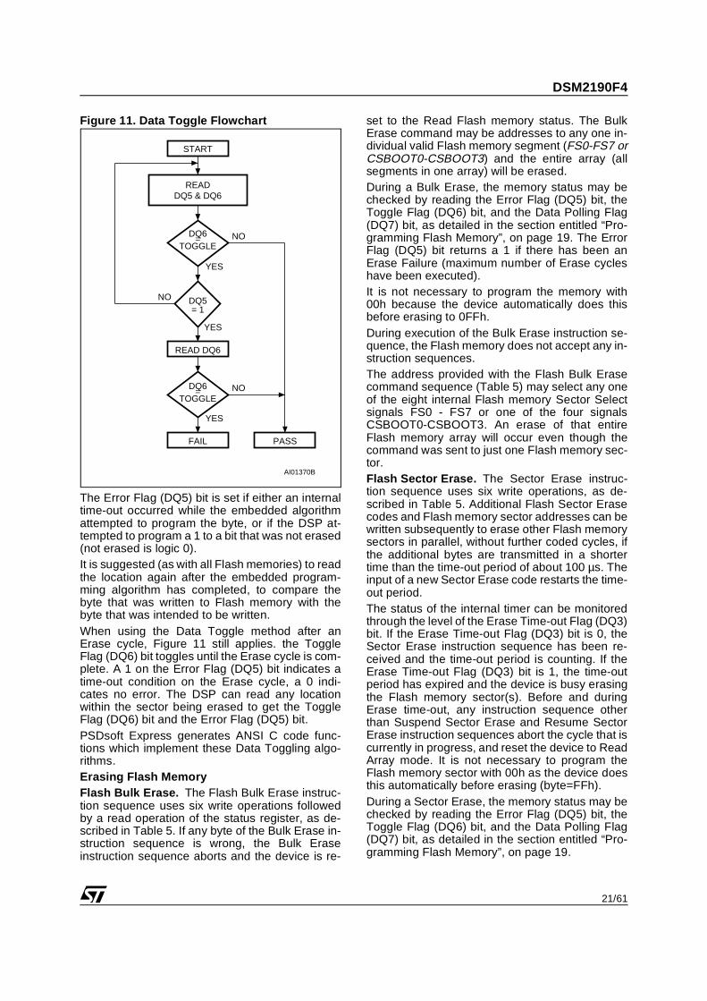
Figure 10. Data Polling Flowchart
Data Toggle. Checking the Toggle Flag (DQ6) bitis a method of determining whether a Program orErase cycle is in progress or has completed. Fig-ure 11 shows the Data Toggle algorithm.When the DSP issues a Program instruction se-quence, the embedded algorithm within the devicebegins. The DSP then reads the location of thebyte to be programmed in Flash memory to checkstatus. The Toggle Flag (DQ6) bit of this locationtoggles each time the DSP reads this location untilthe embedded algorithm is complete. The DSPcontinues to read this location, checking the Tog-gle Flag (DQ6) bit and monitoring the Error Flag(DQ5) bit. When the Toggle Flag (DQ6) bit stopstoggling (two consecutive reads yield the samevalue), and the Error Flag (DQ5) bit remains 0,then the embedded algorithm is complete. If theError Flag (DQ5) bit is 1, the DSP should test theToggle Flag (DQ6) bit again, since the Toggle Flag(DQ6) bit may have changed simultaneously withthe Error Flag (DQ5) bit (see Figure 11).
READ DQ5 & DQ7at VALID ADDRESS
START
READ DQ7
FAIL PASS
AI01369B
DQ7=
DATA
YES
NO
YES
NO
DQ5= 1
DQ7=
DATA
YES
NO
21/61
DSM2190F4
Figure 11. Data Toggle Flowchart
The Error Flag (DQ5) bit is set if either an internaltime-out occurred while the embedded algorithmattempted to program the byte, or if the DSP at-tempted to program a 1 to a bit that was not erased(not erased is logic 0).It is suggested (as with all Flash memories) to readthe location again after the embedded program-ming algorithm has completed, to compare thebyte that was written to Flash memory with thebyte that was intended to be written.When using the Data Toggle method after anErase cycle, Figure 11 still applies. the ToggleFlag (DQ6) bit toggles until the Erase cycle is com-plete. A 1 on the Error Flag (DQ5) bit indicates atime-out condition on the Erase cycle, a 0 indi-cates no error. The DSP can read any locationwithin the sector being erased to get the ToggleFlag (DQ6) bit and the Error Flag (DQ5) bit.PSDsoft Express generates ANSI C code func-tions which implement these Data Toggling algo-rithms.Erasing Flash MemoryFlash Bulk Erase. The Flash Bulk Erase instruc-tion sequence uses six write operations followedby a read operation of the status register, as de-scribed in Table 5. If any byte of the Bulk Erase in-struction sequence is wrong, the Bulk Eraseinstruction sequence aborts and the device is re-
set to the Read Flash memory status. The BulkErase command may be addresses to any one in-dividual valid Flash memory segment (FS0-FS7 orCSBOOT0-CSBOOT3) and the entire array (allsegments in one array) will be erased.During a Bulk Erase, the memory status may bechecked by reading the Error Flag (DQ5) bit, theToggle Flag (DQ6) bit, and the Data Polling Flag(DQ7) bit, as detailed in the section entitled “Pro-gramming Flash Memory”, on page 19. The ErrorFlag (DQ5) bit returns a 1 if there has been anErase Failure (maximum number of Erase cycleshave been executed).It is not necessary to program the memory with00h because the device automatically does thisbefore erasing to 0FFh.During execution of the Bulk Erase instruction se-quence, the Flash memory does not accept any in-struction sequences.The address provided with the Flash Bulk Erasecommand sequence (Table 5) may select any oneof the eight internal Flash memory Sector Selectsignals FS0 - FS7 or one of the four signalsCSBOOT0-CSBOOT3. An erase of that entireFlash memory array will occur even though thecommand was sent to just one Flash memory sec-tor.Flash Sector Erase. The Sector Erase instruc-tion sequence uses six write operations, as de-scribed in Table 5. Additional Flash Sector Erasecodes and Flash memory sector addresses can bewritten subsequently to erase other Flash memorysectors in parallel, without further coded cycles, ifthe additional bytes are transmitted in a shortertime than the time-out period of about 100 µs. Theinput of a new Sector Erase code restarts the time-out period.The status of the internal timer can be monitoredthrough the level of the Erase Time-out Flag (DQ3)bit. If the Erase Time-out Flag (DQ3) bit is 0, theSector Erase instruction sequence has been re-ceived and the time-out period is counting. If theErase Time-out Flag (DQ3) bit is 1, the time-outperiod has expired and the device is busy erasingthe Flash memory sector(s). Before and duringErase time-out, any instruction sequence otherthan Suspend Sector Erase and Resume SectorErase instruction sequences abort the cycle that iscurrently in progress, and reset the device to ReadArray mode. It is not necessary to program theFlash memory sector with 00h as the device doesthis automatically before erasing (byte=FFh).During a Sector Erase, the memory status may bechecked by reading the Error Flag (DQ5) bit, theToggle Flag (DQ6) bit, and the Data Polling Flag(DQ7) bit, as detailed in the section entitled “Pro-gramming Flash Memory”, on page 19.
READDQ5 & DQ6
START
READ DQ6
FAIL PASS
AI01370B
DQ6=
TOGGLENO
NO
YES
YES
DQ5= 1
NO
YES
DQ6=
TOGGLE
DSM2190F4
22/61
During execution of the Erase cycle, the Flashmemory accepts only Reset and Suspend SectorErase instruction sequences. Erasure of oneFlash memory sector may be suspended, in orderto read data from another Flash memory sector,and then resumed.The address provided with the initial Flash SectorErase command sequence (Table 5) must selectthe first desired sector (FS0 - FS7 or CSBOOT0-CSBOOT3) to erase. Subsequent sector erasecommands that are appended on within the time-out period must be addressed to other desiredsegments (FS0 - FS7 or CSBOOT0-CSBOOT3). Suspend Sector Erase. When a Sector Erasecycle is in progress, the Suspend Sector Erase in-struction sequence can be used to suspend thecycle by writing 0B0h to any address when an ap-propriate Sector Select (FS0-FS7 or CSBOOT0-CSBOOT3) is selected (See Table 5). This allowsreading of data from another Flash memory sectorafter the Erase cycle has been suspended. Sus-pend Sector Erase is accepted only during anErase cycle and defaults to Read mode. A Sus-pend Sector Erase instruction sequence executedduring an Erase time-out period, in addition to sus-pending the Erase cycle, terminates the time outperiod.The Toggle Flag (DQ6) bit stops toggling when thedevice internal logic is suspended. The status ofthis bit must be monitored at an address within theFlash memory sector being erased. The ToggleFlag (DQ6) bit stops toggling between 0.1 µs and15 µs after the Suspend Sector Erase instructionsequence has been executed. The device is thenautomatically set to Read mode.If an Suspend Sector Erase instruction sequencewas executed, the following rules apply:– Attempting to read from a Flash memory sector
that was being erased outputs invalid data.– Reading from a Flash memory sector that was
not being erased is valid.
– The Flash memory cannot be programmed, andonly responds to Resume Sector Erase and Re-set Flash instruction sequences (Read is an op-eration and is allowed).
– If a Reset Flash instruction sequence is re-ceived, data in the Flash memory sector thatwas being erased is invalid.
Resume Sector Erase. If a Suspend SectorErase instruction sequence was previously exe-cuted, the erase cycle may be resumed with thisinstruction sequence. The Resume Sector Eraseinstruction sequence consists of writing 030h toany address while an appropriate Sector Select(FS0-FS7 or CSBOOT0-CSBOOT3) is active.(See Table 5.)Flash Memory Sector Protect.Each Flash memory sector can be separately pro-tected against Program and Erase cycles. SectorProtection provides additional data security be-cause it disables all Program or Erase cycles. Thismode can be activated through the JTAG Port or aDevice Programmer. Sector protection can be se-lected for each sector using PSDsoft Express.This automatically protects selected sectors whenthe device is programmed through the JTAG Portor a Device Programmer. Flash memory sectorscan be unprotected to allow updating of their con-tents using the JTAG Port or a Device Program-mer. The DSP can read (but cannot change) thesector protection bits.Any attempt to program or erase a protected Flashmemory sector is ignored by the device. The Verifyoperation results in a read of the protected data.This allows a guarantee of the retention of the Pro-tection status.The sector protection status can be read by theDSP through the Main Flash memory protectionregister (in the csiop block) as defined in Table 7,and Secondary Flash memory protection registerin Table 8.
Table 7. Main Flash Memory Protection Register Definition
Note: Bit Definitions:Sec<i>_Prot 1 = Flash memory sector <i> is write protected.Sec<i>_Prot 0 = Flash memory sector <i> is not write protected.
Table 8. Secondary Flash Memory Protection/Security Bit Register Definition
Note: Security_Bit = 1, device is secured.Note: Sec<i>_Prot 1 = Flash memory sector <i> is write protected.
Sec<i>_Prot 0 = Flash memory sector <i> is not write protected.
Bit 7 Bit 6 Bit 5 Bit 4 Bit 3 Bit 2 Bit 1 Bit 0
Sec7_Prot Sec6_Prot Sec5_Prot Sec4_Prot Sec3_Prot Sec2_Prot Sec1_Prot Sec0_Prot
Bit 7 Bit 6 Bit 5 Bit 4 Bit 3 Bit 2 Bit 1 Bit 0
Security_Bit not used not used not used Sec3_Prot Sec2_Prot Sec1_Prot Sec0_Prot
23/61
DSM2190F4
DSM Security BitA programmable security bit in the DSM protectsits contents from unauthorized viewing and copy-ing. When set, the security bit will block access ofprogramming devices (JTAG or others) to theDSM Flash memory and PLD configuration. Theonly way to defeat the security bit is to erase theentire DSM device, after which the device is blankand may be used again. The DSP will always haveaccess to Flash memory contents through the 8-bitdata port even while the security bit is set. TheDSP can read the status of the security bit (but itcannot change it) by reading the Device Securityregister in the csiop block as defined in Table 8.Reset FlashThe Reset Flash instruction sequence resets theinternal memory logic state machine and putsFlash memory into Read Array mode. It consists ofone write cycle (see Table 5). It must be executedafter:– Reading the Flash Protection Status or Flash ID– An Error condition has occurred (and the device
has set the Error Flag (DQ5) bit to 1) during aFlash memory Program or Erase cycle.
The Reset Flash instruction sequence puts theFlash memory back into normal Read Array mode.It may take the Flash memory up to a few millisec-onds to complete the Reset cycle. The ResetFlash instruction sequence is ignored when it is is-sued during a Program or Bulk Erase cycle of theFlash memory. The Reset Flash instruction se-quence aborts any on-going Sector Erase cycle,and returns the Flash memory to the normal ReadArray mode within a few milliseconds.Page Register The 8-bit Page Register increases the addressingcapability of the DSP by a factor of up to 256. Thecontents of the register can also be read by theDSP. The outputs of the Page Register (PG0-PG7) are inputs to the DPLD decoder and can beincluded in the Sector Select (FS0-FS7 orCSBOOT0-CSBOOT3) equations. See Figure 12.If memory paging is not needed, or if not all 8 pageregister bits are needed for memory paging, thenthese bits may be used in the CPLD for generallogic. The eight flip-flops in the register are con-nected to the internal data bus D0-D7. The DSPcan write to or read from the Page Register. ThePage Register can be accessed at address loca-tion csiop + E0h. Page Register outputs arecleared to logic 0 at reset.
Figure 12. Page Register
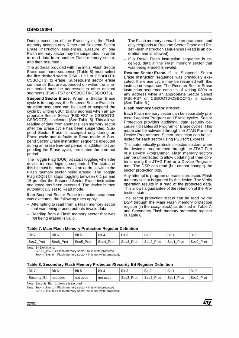
PLDsThe PLDs bring programmable logic to the device.After specifying the logic for the PLDs using PSD-soft Express, the logic is programmed into the de-vice and available upon Power-up.The PLDs have selectable levels of performanceand power consumption. The device contains two PLDs: the Decode PLD(DPLD), and the Complex PLD (CPLD), as shownin Figure 13.
Table 9. DPLD and CPLD Inputs
Note: 1. DSP address lines A16, A17, and others may enter theDSM device on any pin on ports B, C, or D. See Figure 6for recommended connections.
2. Additional DSP control signals may enter the DMS deviceon any pin on Ports B, C, or D. See Figure 6 for recom-mended connections.
Input Source Input Name Number
of Signals
DSP Address Bus1 A15-A0 16
DSP Control Signals2 CNTL2-CNTL0 3
Reset RST 1
PortB Input Macrocells PB7-PB0 8
PortC Input Macrocells PC7-PC0 8
Port D Inputs PD2-PD0 3
Page Register PG7-PG0 8
Macrocell AB Feedback MCELLAB FB7-0 8
Macrocell BC Feedback MCELLBC FB7-0 8
Flash memory Program Status Bit Ready/Busy 1
RESET
D0 - D7
R/W
D0 Q0
Q1
Q2
Q3
Q4
Q5
Q6
Q7
D1
D2
D3
D4
D5
D6
D7
PAGEREGISTER
PGR0
PGR1
PGR2
PGR3 DPLDAND
CPLD
INTERNALSELECTSAND LOGIC
PLD
PGR4
PGR5
PGR6
PGR7
DSM2190F4
24/61
The DPLD performs address decoding, and gen-erates select signals for internal and external com-ponents, such as memory, registers, and I/O ports.The DPLD can generates External Chip Select(ECS0-ECS2) signals on Port D.The CPLD can be used for logic functions, such asloadable counters and shift registers, state ma-chines, and encoding and decoding logic. Theselogic functions can be constructed using the 16Output Macrocells (OMC), 16 Input Macrocells(IMC), and the AND Array. The AND Array is used to form product terms.These product terms are configured from the logicdefinition entered in PSDsoft Express. An InputBus consisting of 64 signals is connected to thePLDs. Input signals are shown in Table 9.
Turbo Bit. The PLDs in the device can minimizepower consumption by switching off when inputsremain unchanged for an extended time of about70 ns. Resetting the Turbo bit to 0 (Bit 3 of thePMMR0 register) automatically places the PLDsinto standby if no inputs are changing. Turning theTurbo mode off increases propagation delayswhile reducing power consumption. Additionally,five bits are available in the PMMR registers incsiop to block DSP control signals from enteringthe PLDs. This reduces power consumption andcan be used only when these DSP control signalsare not used in PLD logic equations. Each of thetwo PLDs has unique characteristics suited for itsapplications. They are described in the followingsections.
Figure 13. PLD Diagram
PLD
INP
UT
BU
S
8
Input Macrocell and Input Ports
Direct Macrocell Input to MCU Data Bus
CSIOP Select
DECODE PLD(DPLD)
PAGEREGISTER
External Chip Selects to Port D
JTAG Select
CPLD
PTALLOC.
MacrocellAlloc.
MCELLAB
MCELLBC
Direct Macrocell Access from MCU Data Bus
16 Input Macrocell(PORT B,C)
16 OutputMacrocell
I/O P
OR
TS
Main Flash Memory Selects
3 PORT D Inputs
to PORT B
to PORT B or C
DataBus
8
8
8
1
3
1
64
16
64
16
Output Macrocell Feedback
4Secondary Flash Memory Selects
AI04957B
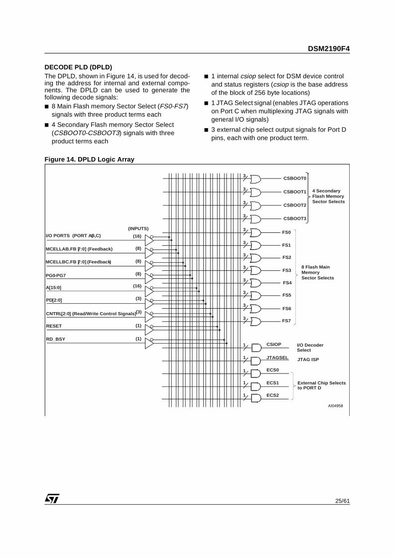
25/61
DSM2190F4
DECODE PLD (DPLD)The DPLD, shown in Figure 14, is used for decod-ing the address for internal and external compo-nents. The DPLD can be used to generate thefollowing decode signals: 8 Main Flash memory Sector Select (FS0-FS7)
signals with three product terms each
4 Secondary Flash memory Sector Select (CSBOOT0-CSBOOT3) signals with three product terms each
1 internal csiop select for DSM device control and status registers (csiop is the base address of the block of 256 byte locations)
1 JTAG Select signal (enables JTAG operations on Port C when multiplexing JTAG signals with general I/O signals)
3 external chip select output signals for Port D pins, each with one product term.
Figure 14. DPLD Logic Array
(INPUTS)
(16)
(8)
(16)
(3)CNTRL[2:0] (Read/Write Control Signals)
I/O PORTS (PORT A,B,C)
(8)PG0-PG7
(8)MCELLAB.FB [7:0] (Feedback)
MCELLBC.FB [7:0] (Feedback)
A[15:0]
(3)
(1)
PD[2:0]
RESET
(1)RD_BSYCSIOP
JTAGSEL
ECS0
ECS1
8 Flash MainMemorySector Selects
I/O DecoderSelect
JTAG ISP
FS0
FS7
3
3
3
3
3
3
3
3
1
ECS2
FS1
FS2
FS3
FS6
FS5
FS4
1
1
1
1
External Chip Selectsto PORT D
CSBOOT0
CSBOOT1
CSBOOT2
CSBOOT3
4 SecondaryFlash MemorySector Selects
3
3
3
3
AI04958

DSM2190F4
26/61
COMPLEX PLD (CPLD)The CPLD can be used to implement system logicfunctions, such as loadable counters and shift reg-isters, system mailboxes, handshaking protocols,state machines, and random logic. See applicationnote AN1171 for details on how to specify logic us-ing PSDsoft Express.As shown in Figure 15, the CPLD has the followingblocks: 16 Input Macrocells (IMC)
16 Output Macrocells (OMC)
Macrocell Allocator
Product Term Allocator
AND Array capable of generating up to 130 product terms
Two I/O Ports.
Each of the blocks are described in the sectionsthat follow.The Input Macrocells (IMC) and Output Macrocells(OMC) are connected to the device internal databus and can be directly accessed by the DSP. Thisenables the DSP software to load data into theOutput Macrocells (OMC) or read data from boththe Input and Output Macrocells (IMC and OMC).This feature allows efficient implementation of sys-tem logic and eliminates the need to connect thedata bus to the AND Array as required in moststandard PLD macro cell architectures.
Figure 15. Macrocell and I/O Port
Output Macrocell (OMC). Eight of the OutputMacrocells (OMC) are connected to Port B pinsand are named as McellAB0-McellAB7. The othereight Macrocells are connected to Ports B or Cpins and are named as McellBC0-McellBC7.OMCs may be used for internal feedback only(buried registers), or their outputs may be routedto external Port pins.
The Output Macrocell (OMC) architecture isshown in Figure 17. As shown in the figure, thereare native product terms available from the ANDArray, and borrowed product terms available (ifunused) from other Output Macrocells (OMC). Thepolarity of the product term is controlled by theXOR gate. The Output Macrocell (OMC) can im-plement either sequential logic, using the flip-flop
I/O PORTSCPLD Macrocells
Input Macrocells
LATCHEDADDRESS OUT
MUX
MU
X
MU
X
MU
X
D
D
Q
Q
Q
G
D
Q D
WR
WR
PDR
DATA
PRODUCT TERMALLOCATOR
DIRREG.
SELECT
INPUT
Product Termsfrom other MacrocellS
POLARITYSELECT
UP TO 10PRODUCT TERMS
CLOCKSELECT
PR DI LD
D/T
CK
CL
Q
D/T/JK FFSELECT
PT CLEAR
PT CLOCK
GLOBAL CLOCK
PT Output Enable (OE)
Macrocell Feedback
I/O Port Input
PT INPUT LATCH GATE/CLOCK
MCU LOAD
PT PRESETMCU DATA IN
COMB./REG
SELECTMacrocell
toI/O PortAlloc.
CPLDOUTPUT
TO OTHER I/O PORTS
PLD
INP
UT
BU
SP
LD IN
PU
T B
US
DSP ADDRESS / DATA BUS
MacrocellOut toMCU
DATALOAD
CONTROL
AN
D A
RR
AY
CPLD OUTPUT
I/O Pin
AI04902B
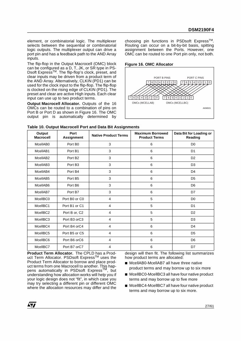
27/61
DSM2190F4
element, or combinatorial logic. The multiplexerselects between the sequential or combinatoriallogic outputs. The multiplexer output can drive aport pin and has a feedback path to the AND Arrayinputs.The flip-flop in the Output Macrocell (OMC) blockcan be configured as a D, T, JK, or SR type in PS-Dsoft ExpressTM. The flip-flop’s clock, preset, andclear inputs may be driven from a product term ofthe AND Array. Alternatively, CLKIN (PD1) can beused for the clock input to the flip-flop. The flip-flopis clocked on the rising edge of CLKIN (PD1). Thepreset and clear are active High inputs. Each clearinput can use up to two product terms.Output Macrocell Allocator. Outputs of the 16OMCs can be routed to a combination of pins onPort B or Port D as shown in Figure 16. The OMCoutput pin is automatically determined by
choosing pin functions in PSDsoft ExpressTM.Routing can occur on a bit-by-bit basis, spittingassignment between the Ports. However, oneOMC can be routed to one Port pin only, not both.
Figure 16. OMC Allocator
Table 10. Output Macrocell Port and Data Bit Assignments
Product Term Allocator. The CPLD has a Prod-uct Term Allocator. PSDsoft ExpressTM uses theProduct Term Allocator to borrow and place prod-uct terms from one Macrocell to another. This hap-pens automatically in PSDsoft ExpressTM, butunderstanding how allocation works will help you ifyour logic design does not “fit”, in which case youmay try selecting a different pin or different OMCwhere the allocation resources may differ and the
design will then fit. The following list summarizeshow product terms are allocated: McellAB0-McellAB7 all have three native
product terms and may borrow up to six more
McellBC0-McellBC3 all have four native product terms and may borrow up to five more
McellBC4-McellBC7 all have four native product terms and may borrow up to six more.
AI04915
PORT C PINSPORT B PINS
OMCs (MCELLBC)OMCs (MCELLAB)
01234567 01234567
4567 3 2 1 04567 3 2 1 0
OutputMacrocell
PortAssignment Native Product Terms Maximum Borrowed
Product TermsData Bit for Loading or
Reading
McellAB0 Port B0 3 6 D0
McellAB1 Port B1 3 6 D1
McellAB2 Port B2 3 6 D2
McellAB3 Port B3 3 6 D3
McellAB4 Port B4 3 6 D4
McellAB5 Port B5 3 6 D5
McellAB6 Port B6 3 6 D6
McellAB7 Port B7 3 6 D7
McellBC0 Port B0 or C0 4 5 D0
McellBC1 Port B1 or C1 4 5 D1
McellBC2 Port B or, C2 4 5 D2
McellBC3 Port B3 orC3 4 5 D3
McellBC4 Port B4 orC4 4 6 D4
McellBC5 Port B5 or C5 4 6 D5
McellBC6 Port B6 orC6 4 6 D6
McellBC7 Port B7 orC7 4 6 D7
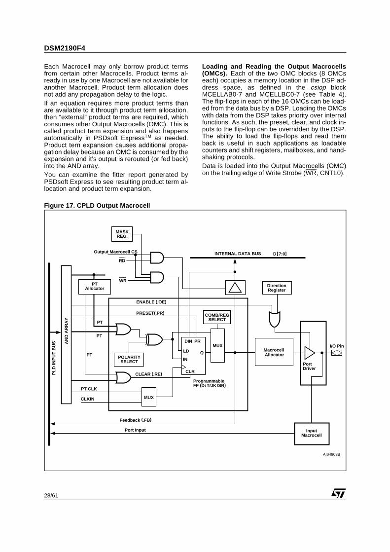
DSM2190F4
28/61
Each Macrocell may only borrow product termsfrom certain other Macrocells. Product terms al-ready in use by one Macrocell are not available foranother Macrocell. Product term allocation doesnot add any propagation delay to the logic.If an equation requires more product terms thanare available to it through product term allocation,then “external” product terms are required, whichconsumes other Output Macrocells (OMC). This iscalled product term expansion and also happensautomatically in PSDsoft ExpressTM as needed.Product tern expansion causes additional propa-gation delay because an OMC is consumed by theexpansion and it’s output is rerouted (or fed back)into the AND array. You can examine the fitter report generated byPSDsoft Express to see resulting product term al-location and product term expansion.
Loading and Reading the Output Macrocells(OMCs). Each of the two OMC blocks (8 OMCseach) occupies a memory location in the DSP ad-dress space, as defined in the csiop blockMCELLAB0-7 and MCELLBC0-7 (see Table 4).The flip-flops in each of the 16 OMCs can be load-ed from the data bus by a DSP. Loading the OMCswith data from the DSP takes priority over internalfunctions. As such, the preset, clear, and clock in-puts to the flip-flop can be overridden by the DSP.The ability to load the flip-flops and read themback is useful in such applications as loadablecounters and shift registers, mailboxes, and hand-shaking protocols.Data is loaded into the Output Macrocells (OMC)on the trailing edge of Write Strobe (WR, CNTL0).
Figure 17. CPLD Output Macrocell
PTAllocator
MASKREG.
PT CLK
PT
PT
PT
CLKIN
Feedback (.FB)
Port Input
AN
D A
RR
AY
PLD
INP
UT
BU
S
MUX
MUX
POLARITYSELECT
LD
IN
CLR
Q
PRDIN
COMB/REGSELECT
PortDriver
InputMacrocell
I/O PinMacrocell Allocator
INTERNAL DATA BUS D[ 7:0]
DirectionRegister
CLEAR (.RE)
ProgrammableFF (D/T/JK /SR)
WR
ENABLE (.OE)
PRESET(.PR)
RD
Output Macrocell CS
AI04903B

29/61
DSM2190F4
The OMC Mask Register. There is one MaskRegister for each of the two groups of eight OutputMacrocells (OMC). The Mask Registers can beused to block the loading of data to individual Out-put Macrocells (OMC). The default value for theMask Registers is 00h, which allows loading of theOutput Macrocells (OMC). When a given bit in aMask Register is set to a 1, the DSP is blockedfrom writing to the associated Output Macrocells(OMC). For example, suppose McellAB0-3 are be-ing used for a state machine. You would not wanta DSP write to McellAB to overwrite the state ma-chine registers. Therefore, you would want to loadthe Mask Register for McellAB (Mask MacrocellAB) with the value 0Fh.
The Output Enable of the OMC. The OutputMacrocells (OMC) block can be connected to an I/O port pin as a PLD output. The output enable ofeach port pin driver is controlled by a single prod-uct term from the AND Array, ORed with the Direc-tion Register output. The pin is enabled uponPower-up if no output enable equation is definedand if the pin is declared as a PLD output in PSD-soft Express.If the Output Macrocell (OMC) output is specifiedas an internal node and not as a port pin output inthe PSDsoft Express, then the port pin can beused for other I/O functions. The internal nodefeedback can be routed as an input to the AND Ar-ray.
Figure 18. Input Macrocell
Input Macrocells (IMC). The CPLD has 16 InputMacrocells (IMC), one for each pin on Ports B andC. The architecture of the IMCs is shown in Figure18. The IMCs are individually configurable, andcan be used as a latch, a register, or to pass in-coming Port signals prior to driving them onto thePLD input bus. This is useful for sampling and de-bouncing inputs to the AND array (keypad inputs,etc.). Additionally, the outputs of the IMCs can beread by the DSP asynchronously at any time
through the internal data bus using the csiop reg-ister block (see Table 4).The enable for the latch and clock for the registerare driven by a product term from the CPLD. Eachproduct term output is used to latch or clock fourIMCs. Port inputs 3-0 can be controlled by oneproduct term and 7-4 by another.Configurations for the IMCs are specified by equa-tions specified in PSDsoft Express. See Applica-tion note AN1171.
OUTPUTMacrocells BC
ANDMacrocells AB
PT
PT
Feedback
AN
D A
RR
AY
PLD
INP
UT
BU
S
PortDriver
I/O Pin
INTERNAL DATA BUS
DIRECTIONREGISTER
MUXPT
Q
Q
D
D
G
LATCH Input Macrocell
ENABLE (.OE)
D FF
INPUT MACROCELL _ RD
AI04904C
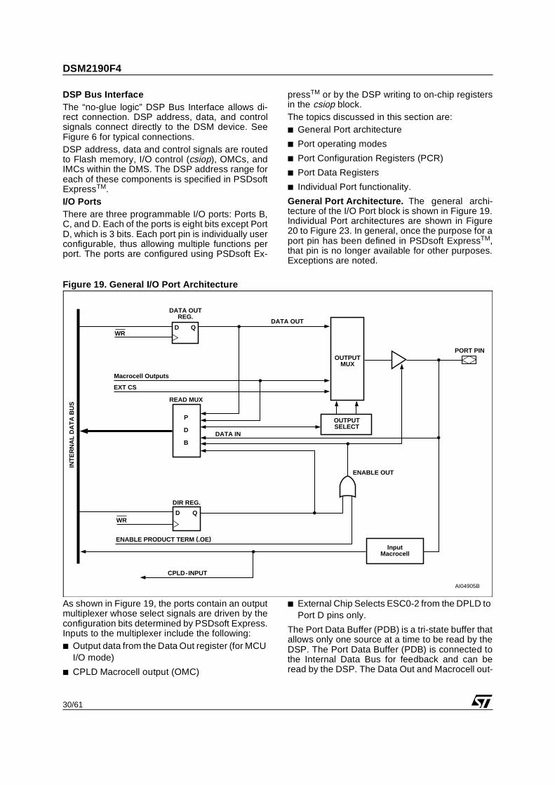
DSM2190F4
30/61
DSP Bus InterfaceThe “no-glue logic” DSP Bus Interface allows di-rect connection. DSP address, data, and controlsignals connect directly to the DSM device. SeeFigure 6 for typical connections.DSP address, data and control signals are routedto Flash memory, I/O control (csiop), OMCs, andIMCs within the DMS. The DSP address range foreach of these components is specified in PSDsoftExpressTM.I/O PortsThere are three programmable I/O ports: Ports B,C, and D. Each of the ports is eight bits except PortD, which is 3 bits. Each port pin is individually userconfigurable, thus allowing multiple functions perport. The ports are configured using PSDsoft Ex-
pressTM or by the DSP writing to on-chip registersin the csiop block.The topics discussed in this section are: General Port architecture
Port operating modes
Port Configuration Registers (PCR)
Port Data Registers
Individual Port functionality.
General Port Architecture. The general archi-tecture of the I/O Port block is shown in Figure 19.Individual Port architectures are shown in Figure20 to Figure 23. In general, once the purpose for aport pin has been defined in PSDsoft ExpressTM,that pin is no longer available for other purposes.Exceptions are noted.
Figure 19. General I/O Port Architecture
As shown in Figure 19, the ports contain an outputmultiplexer whose select signals are driven by theconfiguration bits determined by PSDsoft Express.Inputs to the multiplexer include the following: Output data from the Data Out register (for MCU
I/O mode)
CPLD Macrocell output (OMC)
External Chip Selects ESC0-2 from the DPLD to Port D pins only.
The Port Data Buffer (PDB) is a tri-state buffer thatallows only one source at a time to be read by theDSP. The Port Data Buffer (PDB) is connected tothe Internal Data Bus for feedback and can beread by the DSP. The Data Out and Macrocell out-
INT
ER
NA
L D
AT
A B
US
DATA OUTREG.
D Q
D Q
WR
WR
Macrocell Outputs
ENABLE PRODUCT TERM (.OE)
EXT CS
READ MUX
P
D
B
CPLD-INPUT
DIR REG.
InputMacrocell
ENABLE OUT
DATA IN
OUTPUTSELECT
OUTPUTMUX
PORT PIN
DATA OUT
AI04905B

31/61
DSM2190F4
puts, Direction Registers, and port pin input are allconnected to the Port Data Buffer (PDB).The Port pin’s tri-state output driver enable is con-trolled by a two input OR gate whose inputs comefrom the CPLD AND Array enable product termand the Direction Register. If the enable productterm of any of the Array outputs are not definedand that port pin is not defined as a CPLD outputin PSDsoft ExpressTM, then the Direction Registerhas sole control of the buffer that drives the portpin.The contents of these registers can be altered bythe DSP. The Port Data Buffer (PDB) feedbackpath allows the DSP to check the contents of theregisters.Ports B, and C have embedded IMCs. The IMCscan be configured as registers (for sampling or de-
bouncing), as transparent latches, or direct inputsto the PLDs. The registers and latches are clockedby a product term from the PLD AND Array. Theoutputs from the IMCs drive the PLD input bus andcan be read by the DSP. See the section entitled“Input Macrocell”, on page 29.Port Operating ModesThe I/O Ports have several modes of operation.Modes are defined using PSDsoft ExpressTM, andthen runtime control from the DSP can occur usingthe registers in the csiop block. See ApplicationNote AN1171 for more detail.Table 11 summarizes which modes are availableon each port. Each of the port operating modesare described in the following sections.
Table 11. Port Operating Modes
Note: 1. Can be multiplexed with other I/O functions.
MCU I/O Mode. In the MCU I/O mode, the DSPuses the I/O Ports block to expand its own I/Oports. The DSP can read I/O pins, set the directionof I/O pins, and change the state of I/O pins by ac-cessing the registers in the csiop block. The csiopregister definition and their addresses may befound in Table 4.The MCU I/O direction may be changed by writingto the corresponding bit in the Direction Register,or by the output enable product term. When the pinis configured as an output, the content of the DataOut Register drives the pin. When configured asan input, the DSP can read the port input throughthe Data In buffer. See Figure 19.PLD I/O Mode. Inputs from Ports B and C to ei-ther PLD (DPLD or CPLD) come through IMCs. In-puts from Port D to either PLDs are routed directlyin and do not use IMCs. Outputs from the CPLD toPort B come from the OMC group MCELLAB0-7.Outputs from the CPLD to Port C come from OMCgroup MCELLBC0-7. Outputs from the DPLD toPort D come from the external chip select logicblock ECS0-2. All PLD outputs may be tri-stated at the Port pinswith a control signal. This output enable controlsignal can be defined by a product term from the
PLD, or by resetting the corresponding bit in theDirection Register to 0. The corresponding bit inthe Direction Register must not be set to logic 1 bythe DSP if the pin is defined for a PLD input signalin PSDsoft Express. The PLD I/O mode is definedin PSDsoft Express by specifying PLD equations.JTAG In-System Programming (ISP). Some ofthe pins on Port C are based on the IEEE 1194.1JTAG specification and is used for In-System Pro-gramming (ISP). You can multiplex the function ofthese Port C JTAG pins with other functions. ISPis not performed very frequently in the life of theproduct, so multiplexing these pin’s functions withgeneral purpose I/O functions gives more utilityfrom Port C. See the section entitled “Program-ming In-Circuit Using JTAG ISP”, and ApplicationNote AN1153.Port Configuration Registers (PCR). Each Porthas a set of Port Configuration Registers (PCR)used for configuration of the pins. The contents ofthe registers can be accessed by the DSP throughnormal read/write bus cycles of the csiop registerslisted in Table 4. The pins of a port are individually configurable andeach bit in the register controls its respective pin.For example, Bit 0 in a register refers to Bit 0 of its
Port Mode Port B Port C Port D
MCU I/O Yes Yes Yes
PLD I/OMcellAB Outputs McellBC Outputs Additional External CS Outputs PLD Inputs
Yes Yes No Yes
No Yes No Yes
NoNoYesYes
JTAG ISP No Yes1 No
DSM2190F4
32/61
port. The three Port Configuration Registers(PCR), are shown in Table 12. Default is logic 0.
Table 12. Port Configuration Registers (PCR)
Note: 1. See Table 16 for Drive Register bit definition.
Data In Register. The DSP may read the Data Inregisters in the csiop block at any time to deter-mine the logic state of a Port pin. This will be thestate at the pin regardless of whether it is driven bya source external to the DSM or driven internallyfrom the DSM device. Reading a logic zero for a bitin a Data In register means the corresponding Portpin is also at logic zero. Reading logic one meansthe pin is logic one. Each bit in a Data In registercorresponds to an individual Port pin. For a givenPort, bit 0 in a Data In register corresponds to pin0 of the Port. Example, bit 0 of the Data In registerfor Port B corresponds to Port B pin PB0.Data Out Register. The DSP may write (or read)the Data Out register in the csiop block at anytime. Writing the Data Out register will change thelogic state of a Port pin only if it is not driven orcontrolled by the CPLD. Writing a logic zero to a bitin a Data Out register will force the correspondingPort pin to be logic zero. Writing logic one will drivethe pin to logic one. Each bit in the Data Out reg-isters correspond to Port pins the same way as theData In registers described above. When somepins of a Port are driven by the CPLD, writing tothe corresponding bit in a Data Out register willhave no effect as the CPLD overrides the Data Outregister.Direction Register. The Direction Register, inconjunction with the output enable (except for PortD), controls the direction of data flow in the I/OPorts. Any bit set to 1 in the Direction Registercauses the corresponding pin to be an output, andany bit set to 0 causes it to be an input. The defaultmode for all port pins is input.
Table 13. Port Pin Direction Control, Output Enable P.T. Not Defined
Table 14. Port Pin Direction Control, Output Enable P.T. Defined
Table 15. Port Direction Assignment Example
Figure 20 and Figure 21 show the Port Architec-ture diagrams for Ports B and C, respectively. Thedirection of data flow for Ports B, and C are con-trolled not only by the direction register, but also bythe output enable product term from the PLD ANDArray. If the output enable product term is not ac-tive, the Direction Register has sole control of agiven pin’s direction.An example of a configuration for a Port with thethree least significant bits set to output and the re-mainder set to input is shown in Table 15. SincePort D only contains three pins (shown in Figure23), the Direction Register for Port D has only thethree least significant bits active.Drive Select Register. The Drive Select Registerconfigures the pin driver as Open Drain or CMOS(standard push/pull) for some port pins, and con-trols the slew rate for the other port pins. An exter-nal pull-up resistor should be used for pinsconfigured as Open Drain. Open Drain outputs arediode clamped, thus the maximum voltage on anpin configured as Open Drain is Vcc + 0.7V.A pin can be configured as Open Drain if its corre-sponding bit in the Drive Select Register is set to a1. The default pin drive is CMOS.Note that the slew rate is a measurement of therise and fall times of an output. A higher slew ratemeans a faster output response and may createmore electrical noise. A pin operates in a high slewrate when the corresponding bit in the Drive Reg-ister is set to 1. The default rate is standard slew.Table 16 shows the Drive Register for Ports B, C,and D. It summarizes which pins can be config-ured as Open Drain outputs and which pins theslew rate can be set for.
Register Name Port DSP Access
Data In B,C,D Read
Data Out B,C,D Write/Read
Direction B,C,D Write/Read
Drive Select1 B,C,D Write/Read
Direction Register Bit Port Pin Mode
0 Input
1 Output
Direction Register Bit
Output Enable P.T. Port Pin Mode
0 0 Input
0 1 Output
1 0 Output
1 1 Output
Bit 7 Bit 6 Bit 5 Bit 4 Bit 3 Bit 2 Bit 1 Bit 0
0 0 0 0 0 1 1 1
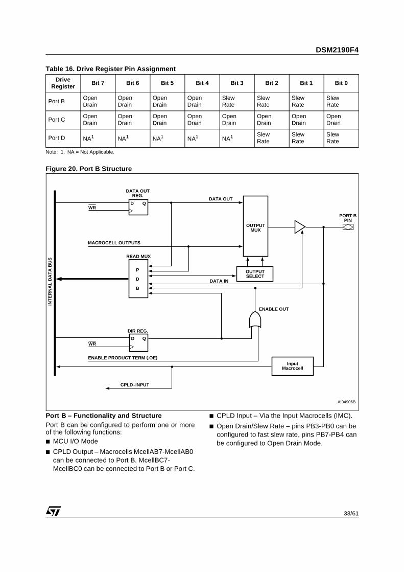
33/61
DSM2190F4
Table 16. Drive Register Pin Assignment
Note: 1. NA = Not Applicable.
Figure 20. Port B Structure
Port B – Functionality and StructurePort B can be configured to perform one or moreof the following functions: MCU I/O Mode
CPLD Output – Macrocells McellAB7-McellAB0 can be connected to Port B. McellBC7-McellBC0 can be connected to Port B or Port C.
CPLD Input – Via the Input Macrocells (IMC).
Open Drain/Slew Rate – pins PB3-PB0 can be configured to fast slew rate, pins PB7-PB4 can be configured to Open Drain Mode.
Drive Register Bit 7 Bit 6 Bit 5 Bit 4 Bit 3 Bit 2 Bit 1 Bit 0
Port BOpenDrain
OpenDrain
OpenDrain
OpenDrain
SlewRate
SlewRate
SlewRate
SlewRate
Port COpenDrain
OpenDrain
OpenDrain
OpenDrain
OpenDrain
OpenDrain
OpenDrain
OpenDrain
Port D NA1 NA1 NA1 NA1 NA1 SlewRate
SlewRate
SlewRate
INT
ER
NA
L D
AT
A B
US
DATA OUTREG.
D Q
D Q
WR
WR
MACROCELL OUTPUTS
ENABLE PRODUCT TERM (.OE)
READ MUX
P
D
B
CPLD-INPUT
DIR REG.
InputMacrocell
ENABLE OUT
DATA IN
OUTPUTSELECT
OUTPUTMUX
PORT BPIN
DATA OUT
AI04906B
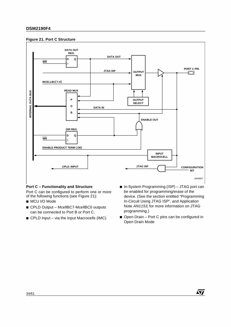
DSM2190F4
34/61
Figure 21. Port C Structure
Port C – Functionality and StructurePort C can be configured to perform one or moreof the following functions (see Figure 21): MCU I/O Mode
CPLD Output – McellBC7-McellBC0 outputs can be connected to Port B or Port C.
CPLD Input – via the Input Macrocells (IMC)
In-System Programming (ISP) – JTAG port can be enabled for programming/erase of the device. (See the section entitled “Programming In-Circuit Using JTAG ISP”, and Application Note AN1153, for more information on JTAG programming.)
Open Drain – Port C pins can be configured in Open Drain Mode
INT
ER
NA
L D
AT
A B
US
DATA OUTREG.
D Q
D Q
WR
WR
MCELLBC [ 7:0]
ENABLE PRODUCT TERM (.OE)
READ MUX
P
D
B
CPLD-INPUT
DIR REG.
INPUTMACROCELL
ENABLE OUT
JTAG ISP
JTAG ISP
CONFIGURATIONBIT
DATA IN
OUTPUTSELECT
OUTPUTMUX
PORT C PIN
DATA OUT
AI04907
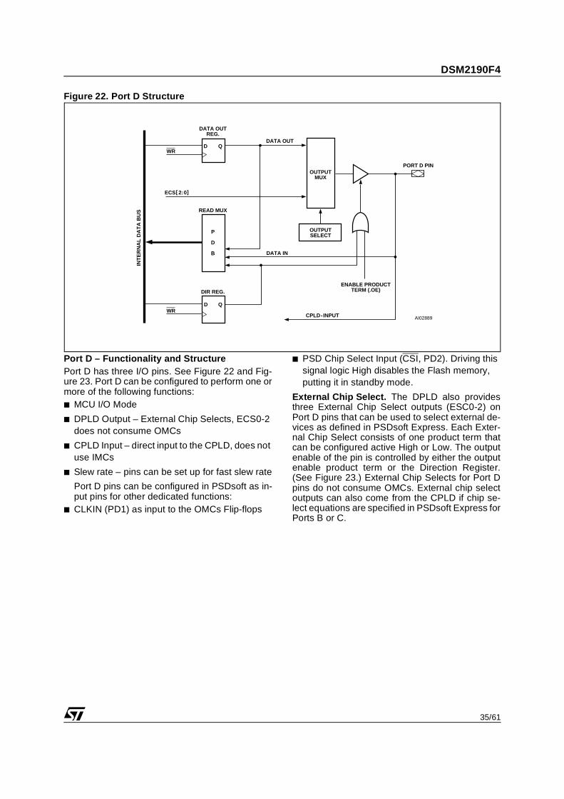
35/61
DSM2190F4
Figure 22. Port D Structure
Port D – Functionality and StructurePort D has three I/O pins. See Figure 22 and Fig-ure 23. Port D can be configured to perform one ormore of the following functions: MCU I/O Mode
DPLD Output – External Chip Selects, ECS0-2 does not consume OMCs
CPLD Input – direct input to the CPLD, does not use IMCs
Slew rate – pins can be set up for fast slew rate
Port D pins can be configured in PSDsoft as in-put pins for other dedicated functions:
CLKIN (PD1) as input to the OMCs Flip-flops
PSD Chip Select Input (CSI, PD2). Driving this signal logic High disables the Flash memory, putting it in standby mode.
External Chip Select. The DPLD also providesthree External Chip Select outputs (ESC0-2) onPort D pins that can be used to select external de-vices as defined in PSDsoft Express. Each Exter-nal Chip Select consists of one product term thatcan be configured active High or Low. The outputenable of the pin is controlled by either the outputenable product term or the Direction Register.(See Figure 23.) External Chip Selects for Port Dpins do not consume OMCs. External chip selectoutputs can also come from the CPLD if chip se-lect equations are specified in PSDsoft Express forPorts B or C.
INT
ER
NA
L D
AT
A B
US
DATA OUTREG.
D Q
D Q
WR
WR
ECS[ 2:0]
READ MUX
P
D
B
CPLD-INPUT
DIR REG.
DATA IN
ENABLE PRODUCTTERM (.OE)
OUTPUTSELECT
OUTPUTMUX
PORT D PIN
DATA OUT
AI02889
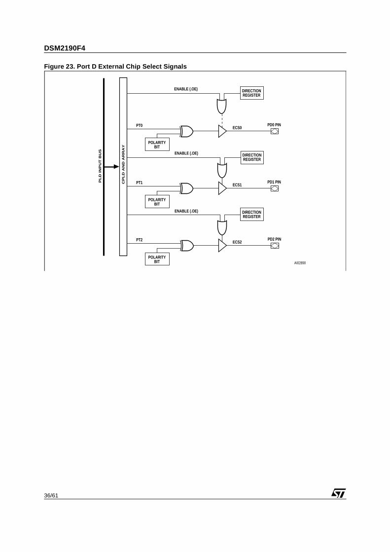
DSM2190F4
36/61
Figure 23. Port D External Chip Select Signals
PL
D I
NP
UT
BU
S
POLARITYBIT
PD2 PINPT2 ECS2
DIRECTIONREGISTER
POLARITYBIT
PD1 PINPT1 ECS1
ENABLE (.OE)
ENABLE (.OE) DIRECTIONREGISTER
POLARITYBIT
PD0 PINPT0 ECS0
ENABLE (.OE) DIRECTIONREGISTER
CP
LD
AN
D A
RR
AY
AI02890
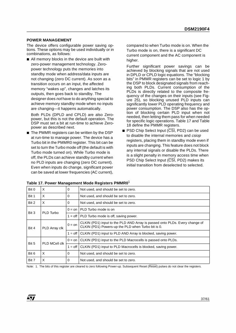
37/61
DSM2190F4
POWER MANAGEMENTThe device offers configurable power saving op-tions. These options may be used individually or incombinations, as follows: All memory blocks in the device are built with
zero-power management technology. Zero-power technology puts the memories into standby mode when address/data inputs are not changing (zero DC current). As soon as a transition occurs on an input, the affected memory “wakes up”, changes and latches its outputs, then goes back to standby. The designer does not have to do anything special to achieve memory standby mode when no inputs are changing—it happens automatically.
Both PLDs (DPLD and CPLD) are also Zero-power, but this is not the default operation. TheDSP must set a bit at run-time to achieve Zero-power as described next.
The PMMR registers can be written by the DSP at run-time to manage power. The device has a Turbo bit in the PMMR0 register. This bit can be set to turn the Turbo mode off (the default is with Turbo mode turned on). While Turbo mode is off, the PLDs can achieve standby current when no PLD inputs are changing (zero DC current). Even when inputs do change, significant power can be saved at lower frequencies (AC current),
compared to when Turbo mode is on. When the Turbo mode is on, there is a significant DC current component and the AC component is higher.
Further significant power savings can beachieved by blocking signals that are not usedin DPLD or CPLD logic equations. The “blockingbits” in PMMR registers can be set to logic 1 bythe DSP to block designated signals from reach-ing both PLDs. Current consumption of thePLDs is directly related to the composite fre-quency of the changes on their inputs (see Fig-ure 25), so blocking unused PLD inputs cansignificantly lower PLD operating frequency andpower consumption. The DSP also has the op-tion of blocking certain PLD input when notneeded, then letting them pass for when neededfor specific logic operations. Table 17 and Table18 define the PMMR registers.
PSD Chip Select Input (CSI, PD2) can be used to disable the internal memories and csiop registers, placing them in standby mode even if inputs are changing. This feature does not block any internal signals or disable the PLDs. There is a slight penalty in memory access time when PSD Chip Select Input (CSI, PD2) makes its initial transition from deselected to selected.
Table 17. Power Management Mode Registers PMMR01
Note: 1. The bits of this register are cleared to zero following Power-up. Subsequent Reset (Reset) pulses do not clear the registers.
Bit 0 X 0 Not used, and should be set to zero.
Bit 1 X 0 Not used, and should be set to zero.
Bit 2 X 0 Not used, and should be set to zero.
Bit 3 PLD Turbo0 = on PLD Turbo mode is on
1 = off PLD Turbo mode is off, saving power.
Bit 4 PLD Array clk0 = on
CLKIN (PD1) input to the PLD AND Array is passed onto PLDs. Every change of CLKIN (PD1) Powers-up the PLD when Turbo bit is 0.
1 = off CLKIN (PD1) input to PLD AND Array is blocked, saving power.
Bit 5 PLD MCell clk0 = on CLKIN (PD1) input to the PLD Macrocells is passed onto PLDs.
1 = off CLKIN (PD1) input to PLD Macrocells is blocked, saving power.
Bit 6 X 0 Not used, and should be set to zero.
Bit 7 X 0 Not used, and should be set to zero.
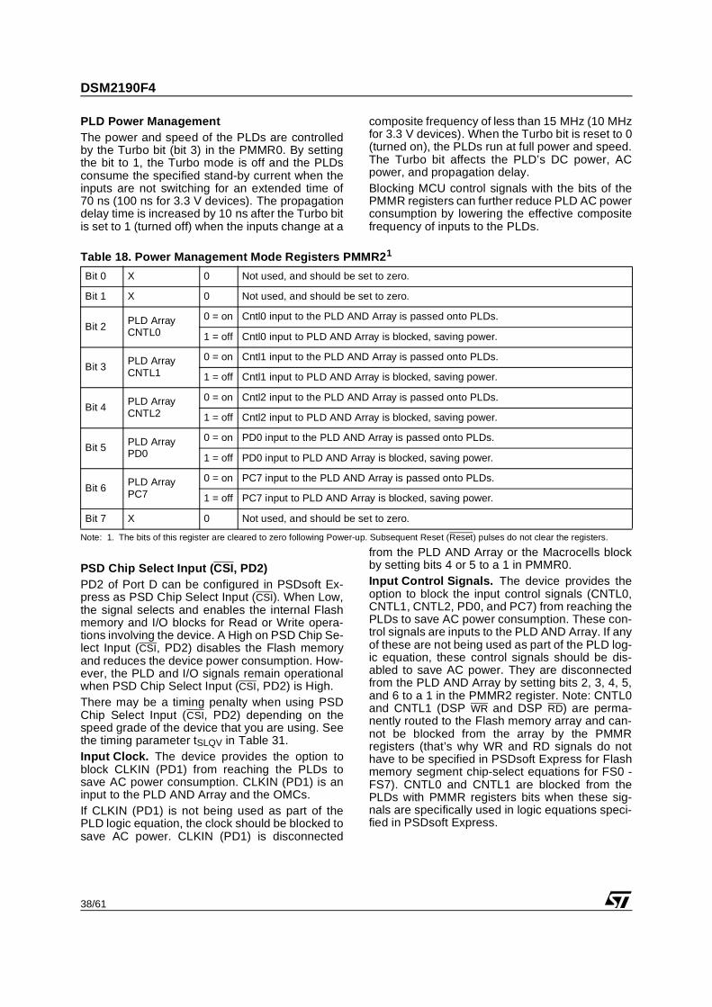
DSM2190F4
38/61
PLD Power ManagementThe power and speed of the PLDs are controlledby the Turbo bit (bit 3) in the PMMR0. By settingthe bit to 1, the Turbo mode is off and the PLDsconsume the specified stand-by current when theinputs are not switching for an extended time of70 ns (100 ns for 3.3 V devices). The propagationdelay time is increased by 10 ns after the Turbo bitis set to 1 (turned off) when the inputs change at a
composite frequency of less than 15 MHz (10 MHzfor 3.3 V devices). When the Turbo bit is reset to 0(turned on), the PLDs run at full power and speed.The Turbo bit affects the PLD’s DC power, ACpower, and propagation delay.Blocking MCU control signals with the bits of thePMMR registers can further reduce PLD AC powerconsumption by lowering the effective compositefrequency of inputs to the PLDs.
Table 18. Power Management Mode Registers PMMR21
Note: 1. The bits of this register are cleared to zero following Power-up. Subsequent Reset (Reset) pulses do not clear the registers.
PSD Chip Select Input (CSI, PD2)PD2 of Port D can be configured in PSDsoft Ex-press as PSD Chip Select Input (CSI). When Low,the signal selects and enables the internal Flashmemory and I/O blocks for Read or Write opera-tions involving the device. A High on PSD Chip Se-lect Input (CSI, PD2) disables the Flash memoryand reduces the device power consumption. How-ever, the PLD and I/O signals remain operationalwhen PSD Chip Select Input (CSI, PD2) is High.There may be a timing penalty when using PSDChip Select Input (CSI, PD2) depending on thespeed grade of the device that you are using. Seethe timing parameter tSLQV in Table 31.Input Clock. The device provides the option toblock CLKIN (PD1) from reaching the PLDs tosave AC power consumption. CLKIN (PD1) is aninput to the PLD AND Array and the OMCs.If CLKIN (PD1) is not being used as part of thePLD logic equation, the clock should be blocked tosave AC power. CLKIN (PD1) is disconnected
from the PLD AND Array or the Macrocells blockby setting bits 4 or 5 to a 1 in PMMR0.Input Control Signals. The device provides theoption to block the input control signals (CNTL0,CNTL1, CNTL2, PD0, and PC7) from reaching thePLDs to save AC power consumption. These con-trol signals are inputs to the PLD AND Array. If anyof these are not being used as part of the PLD log-ic equation, these control signals should be dis-abled to save AC power. They are disconnectedfrom the PLD AND Array by setting bits 2, 3, 4, 5,and 6 to a 1 in the PMMR2 register. Note: CNTL0and CNTL1 (DSP WR and DSP RD) are perma-nently routed to the Flash memory array and can-not be blocked from the array by the PMMRregisters (that’s why WR and RD signals do nothave to be specified in PSDsoft Express for Flashmemory segment chip-select equations for FS0 -FS7). CNTL0 and CNTL1 are blocked from thePLDs with PMMR registers bits when these sig-nals are specifically used in logic equations speci-fied in PSDsoft Express.
Bit 0 X 0 Not used, and should be set to zero.
Bit 1 X 0 Not used, and should be set to zero.
Bit 2PLD Array CNTL0
0 = on Cntl0 input to the PLD AND Array is passed onto PLDs.
1 = off Cntl0 input to PLD AND Array is blocked, saving power.
Bit 3PLD Array CNTL1
0 = on Cntl1 input to the PLD AND Array is passed onto PLDs.
1 = off Cntl1 input to PLD AND Array is blocked, saving power.
Bit 4PLD Array CNTL2
0 = on Cntl2 input to the PLD AND Array is passed onto PLDs.
1 = off Cntl2 input to PLD AND Array is blocked, saving power.
Bit 5 PLD Array PD0
0 = on PD0 input to the PLD AND Array is passed onto PLDs.
1 = off PD0 input to PLD AND Array is blocked, saving power.
Bit 6PLD Array PC7
0 = on PC7 input to the PLD AND Array is passed onto PLDs.
1 = off PC7 input to PLD AND Array is blocked, saving power.
Bit 7 X 0 Not used, and should be set to zero.
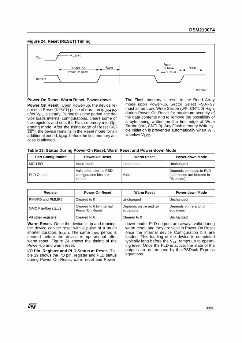
39/61
DSM2190F4
Figure 24. Reset (RESET) Timing
Power On Reset, Warm Reset, Power-downPower On Reset. Upon Power-up, the device re-quires a Reset (RESET) pulse of duration tNLNH-POafter VCC is steady. During this time period, the de-vice loads internal configurations, clears some ofthe registers and sets the Flash memory into Op-erating mode. After the rising edge of Reset (RE-SET), the device remains in the Reset mode for anadditional period, tOPR, before the first memory ac-cess is allowed.
The Flash memory is reset to the Read Arraymode upon Power-up. Sector Select FS0-FS7must all be Low, Write Strobe (WR, CNTL0) High,during Power On Reset for maximum security ofthe data contents and to remove the possibility ofa byte being written on the first edge of WriteStrobe (WR, CNTL0). Any Flash memory Write cy-cle initiation is prevented automatically when VCCis below VLKO.
Table 19. Status During Power-On Reset, Warm Reset and Power-down Mode
Warm Reset. Once the device is up and running,the device can be reset with a pulse of a muchshorter duration, tNLNH. The same tOPR period isneeded before the device is operational afterwarm reset. Figure 24 shows the timing of thePower-up and warm reset.I/O Pin, Register and PLD Status at Reset. Ta-ble 19 shows the I/O pin, register and PLD statusduring Power On Reset, warm reset and Power-
down mode. PLD outputs are always valid duringwarm reset, and they are valid in Power On Resetonce the internal device Configuration bits areloaded. This loading of the device is completedtypically long before the VCC ramps up to operat-ing level. Once the PLD is active, the state of theoutputs are determined by the PSDsoft Expressequations.
tNLNH-PO tOPR
AI02866b
RESET
tNLNHtNLNH-A tOPR
VCCVCC(min)
Power-On Reset Warm Reset
Port Configuration Power-On Reset Warm Reset Power-down Mode
MCU I/O Input mode Input mode Unchanged
PLD Output Valid after internal PSD configuration bits are loaded
Valid Depends on inputs to PLD (addresses are blocked in PD mode)
Register Power-On Reset Warm Reset Power-down Mode
PMMR0 and PMMR2 Cleared to 0 Unchanged Unchanged
OMC Flip-flop statusCleared to 0 by internal Power-On Reset
Depends on .re and .pr equations
Depends on .re and .pr equations
All other registers Cleared to 0 Cleared to 0 Unchanged
DSM2190F4
40/61
PROGRAMMING IN-CIRCUIT USING JTAG ISPIn-System Programming (ISP) can be performedthrough the JTAG signals on Port C. This serial in-terface allows programming of the entire DSM de-vice or subsections (i.e. only Flash memory but notthe PLDs) without and participation of the DSP. Ablank DSM device soldered to a circuit board canbe completely programmed in 10 to 25 seconds.The basic JTAG signals; TMS, TCK, TDI, andTDO form the IEEE-1149.1 interface. The DSMdevice does not implement the IEEE-1149.1Boundary Scan functions. The DSM uses theJTAG interface for ISP only. However, the DSMdevice can reside in a standard JTAG chain withother JTAG devices as it will remain in BYPASSmode while other devices perform BoundaryScan. ISP programming time can be reduced as much as30% by using two more signals on Port C, TSTATand TERR in addition to TMS, TCK, TDI and TDO.See Table 20. The FlashLINKTM JTAG program-ming cable available from STMicroelectronics for$59USD and PSDsoft Express software that isavailable at no charge from www.st.com/psm is allthat is needed to program a DSM device using theparallel port on any PC or laptop.By default, the four pins on Port C are enabled forthe basic JTAG signals TMS, TCK, TDI, and TDOon a blank device (and as shipped from factory)See Application Note AN1153 for more details onJTAG In-System Programming (ISP).Standard JTAG Signals. The standard JTAGsignals (TMS, TCK, TDI, and TDO) can be en-abled by any of three different conditions that arelogically ORed. The following symbolic logic equation specifies theconditions enabling the four basic JTAG signals(TMS, TCK, TDI, and TDO) on their respectivePort C pins. For purposes of discussion, the logiclabel JTAG_ON is used. When JTAG_ON is true,the four pins are enabled for JTAG operation.When JTAG_ON is false, the four pins can beused for general device I/O as specified in PSD-soft Express. JTAG_ON can become true by anyof three different ways as shown:
JTAG_ON = 1. PSDsoft Express Pin Configuration -OR-2. PSDsoft Express PLD equation -OR-3. DSP writes to register in csiop block
Method 1 is most common. This is when the JTAGpins are selected in PSDsoft Express to be “dedi-cated” JTAG pins. They can always transmit andreceive JTAG information because they are “full-time” JTAG pins.
Method 2 is used only when the JTAG pins aremultiplexed with general I/O functions. For de-signs that need every I/O pin, the JTAG pins maybe used for general I/O when they are not used forISP. However, when JTAG pins are multiplexedwith general I/O functions, the designer must in-clude a way to get the pins back into JTAG modewhen it is time for JTAG operations again. In thiscase, a single PLD input from Ports B, C, or Dmust be dedicated to switch the Port C pins from I/O mode back to ISP mode at any time. It is recom-mended to physically connect this dedicated PLDinput pin to the JEN\ output signal from theFlashlink cable when multiplexing JTAG signals.See Application Note AN1153 for details.Method 3 is rarely used to control JTAG pin oper-ation. The DSP can set the port C pins to functionas JTAG ISP by setting the JTAG Enable bit in aregister of the csiop block, but as soon as the DSMchip is reset, the csiop block registers are cleared,which turns off the JTAG-ISP function. ControllingJTAG pins using this method is not recommended.
Table 20. JTAG Port Signals
JTAG Extensions. TSTAT and TERR are twoJTAG extension signals (must be used as a pair)enabled by a command received over the fourstandard JTAG signals (TMS, TCK, TDI, andTDO) by PSDsoft Express. They are used tospeed Program and Erase cycles by indicatingstatus on device pins instead of having to scan thestatus out serially using the standard JTAG chan-nel. See Application Note AN1153.TERR indicates if an error has occurred whenerasing a sector or programming a byte in Flashmemory. This signal goes Low (active) when anError condition occurs.TSTAT behaves the same as Ready/Busy de-scribed previously. TSTAT is inactive logic 1 whenthe device is in Read mode (Flash memory con-tents can be read). TSTAT is logic 0 when Flashmemory Program or Erase cycles are in progress.TSTAT and TERR can be configured as open-drain type signals with PSDsoft Express. This fa-cilitates a wired-OR connection of TSTAT signals
Port C Pin JTAG Signals Description
PC0 TMS Mode Select
PC1 TCK Clock
PC3 TSTAT Status
PC4 TERR Error Flag
PC5 TDI Serial Data In
PC6 TDO Serial Data Out

41/61
DSM2190F4
from multiple DSM2190F4V devices and a wired-OR connection of TERR signals from those samedevices. This is useful when several devices are“chained” together in a JTAG environment. PSD-soft Express puts TSTAT and TERR signals toopen-drain by default. Click on 'Properties' in theJTAG-ISP window of PSDsoft Express to changeto standard CMOS push-pull. It is recommendedto use 10 kΩ pull-up resistors to VCC on all JTAG-ISP signals on your circuit board.
Initial Delivery StateWhen delivered from ST, the device has all bits inthe memory and PLDs erased to logic 1. The DSMConfiguration Register bits are set to 0. The code,configuration, and PLD logic are loaded using theprogramming procedure. The four basic JTAG ISPsignals (TCK, TMS, TDI, TDO) are ready for ISPfunction.

DSM2190F4
42/61
AC/DC PARAMETERSThese tables describe the AC and DC parametersof the device: DC Electrical Specification AC Timing Specification PLD Timing
– Combinatorial Timing
– Synchronous Clock Mode
– Asynchronous Clock Mode
– Input Macrocell Timing
DSP Timing
– Read Timing
– Write Timing
– Reset Timing
The following are issues concerning the parame-ters presented:
In the DC specification the supply current is given for different modes of operation. Before calculating the total power consumption, determine the percentage of time that the device is in each mode. Also, the supply power is considerably different if the Turbo bit is 0.
The AC power component gives the PLD and Flash memory a mA/MHz specification. Figure 25 shows the PLD mA/MHz as a function of the number of Product Terms (PT) used.
The fitter report of PSDsoft Express indicates the number of Product Terms (PTs) used for a given design. This number may be used to estimate PLD power consumption using Figure 25.
In the PLD timing parameters, add the required delay when Turbo bit is 0.
Figure 25. PLD ICC /Frequency Consumption (3.3 V)
0
10
20
30
40
50
60VCC = 3V
0 10 155 20 25
I CC
– (
mA
)
TURBO ON (100%)
TURBO ON (25%)
TURBO O
FF
TURBO OFF
HIGHEST COMPOSITE FREQUENCY AT PLD INPUTS (MHz)
PT 100%PT 25%
AI03100
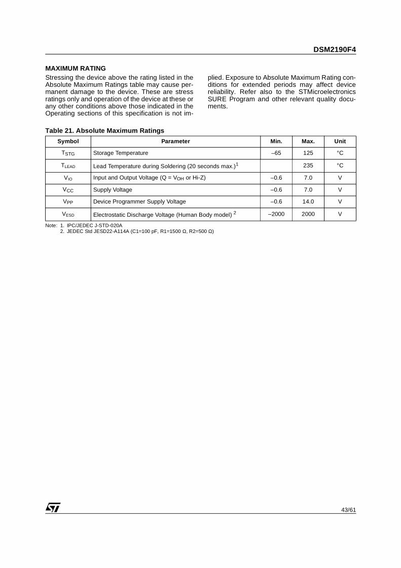
43/61
DSM2190F4
MAXIMUM RATINGStressing the device above the rating listed in theAbsolute Maximum Ratings table may cause per-manent damage to the device. These are stressratings only and operation of the device at these orany other conditions above those indicated in theOperating sections of this specification is not im-
plied. Exposure to Absolute Maximum Rating con-ditions for extended periods may affect devicereliability. Refer also to the STMicroelectronicsSURE Program and other relevant quality docu-ments.
Table 21. Absolute Maximum Ratings
Note: 1. IPC/JEDEC J-STD-020A2. JEDEC Std JESD22-A114A (C1=100 pF, R1=1500 Ω, R2=500 Ω)
Symbol Parameter Min. Max. Unit
TSTG Storage Temperature –65 125 °C
TLEAD Lead Temperature during Soldering (20 seconds max.)1 235 °C
VIO Input and Output Voltage (Q = VOH or Hi-Z) –0.6 7.0 V
VCC Supply Voltage –0.6 7.0 V
VPP Device Programmer Supply Voltage –0.6 14.0 V
VESD Electrostatic Discharge Voltage (Human Body model) 2 –2000 2000 V
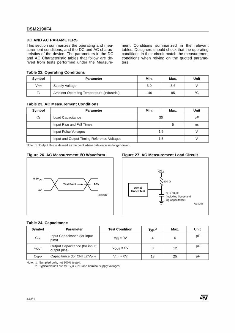
DSM2190F4
44/61
DC AND AC PARAMETERSThis section summarizes the operating and mea-surement conditions, and the DC and AC charac-teristics of the device. The parameters in the DCand AC Characteristic tables that follow are de-rived from tests performed under the Measure-
ment Conditions summarized in the relevanttables. Designers should check that the operatingconditions in their circuit match the measurementconditions when relying on the quoted parame-ters.
Table 22. Operating Conditions
Table 23. AC Measurement Conditions
Note: 1. Output Hi-Z is defined as the point where data out is no longer driven.
Figure 26. AC Measurement I/O Waveform Figure 27. AC Measurement Load Circuit
Table 24. Capacitance
Note: 1. Sampled only, not 100% tested.2. Typical values are for TA = 25°C and nominal supply voltages.
Symbol Parameter Min. Max. Unit
VCC Supply Voltage 3.0 3.6 V
TA Ambient Operating Temperature (industrial) –40 85 °C
Symbol Parameter Min. Max. Unit
CL Load Capacitance 30 pF
Input Rise and Fall Times 5 ns
Input Pulse Voltages 1.5 V
Input and Output Timing Reference Voltages 1.5 V
0.9VCC
0V
Test Point 1.5V
AI04947
DeviceUnder Test
2.0 V
400 Ω
CL = 30 pF(Including Scope andJig Capacitance)
AI04948
Symbol Parameter Test Condition Typ.2 Max. Unit
CINInput Capacitance (for input pins)
VIN = 0V 4 6pF
COUTOutput Capacitance (for input/output pins)
VOUT = 0V 8 12pF
CVPP Capacitance (for CNTL2/VPP) VPP = 0V 18 25 pF

45/61
DSM2190F4
Table 25. AC Symbols for PLD Timing
Example: tAVWL – Time from Address Valid toWrite input Low.
Figure 28. Switching Waveforms – Key
Signal Letters Signal Behavior
A Address Input t Time
C CEout Output L Logic Level Low
D Input Data H Logic Level High
E E Input V Valid
N Reset Input or Output X No Longer a Valid Logic Level
P Port Signal Output Z Float
Q Output Data PW Pulse Width
R RD Input (read)
S Chip Select Input, BMS, DMS, IOMS, or FSx
W WR Input (write)
B VSTBY Output
M Output Macrocell
WAVEFORMS INPUTS OUTPUTS
STEADY INPUT
MAY CHANGE FROMHI TO LO
MAY CHANGE FROMLO TO HI
DON'T CARE
OUTPUTS ONLY
STEADY OUTPUT
WILL BE CHANGINGFROM HI TO LO
WILL BE CHANGINGLO TO HI
CHANGING, STATEUNKNOWN
CENTER LINE ISTRI-STATE
AI03102
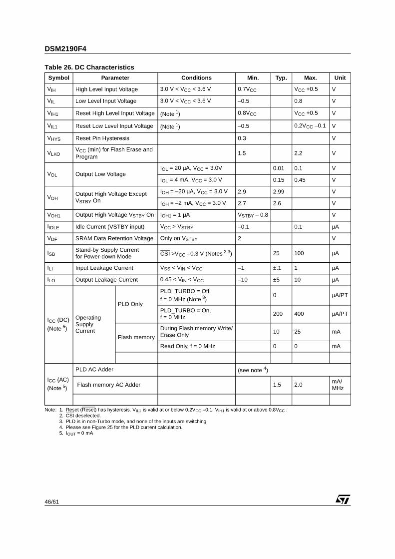
DSM2190F4
46/61
Table 26. DC Characteristics
Note: 1. Reset (Reset) has hysteresis. VIL1 is valid at or below 0.2VCC –0.1. VIH1 is valid at or above 0.8VCC .2. CSI deselected.3. PLD is in non-Turbo mode, and none of the inputs are switching.4. Please see Figure 25 for the PLD current calculation.5. IOUT = 0 mA
Symbol Parameter Conditions Min. Typ. Max. Unit
VIH High Level Input Voltage 3.0 V < VCC < 3.6 V 0.7VCC VCC +0.5 V
VIL Low Level Input Voltage 3.0 V < VCC < 3.6 V –0.5 0.8 V
VIH1 Reset High Level Input Voltage (Note 1) 0.8VCC VCC +0.5 V
VIL1 Reset Low Level Input Voltage (Note 1) –0.5 0.2VCC –0.1 V
VHYS Reset Pin Hysteresis 0.3 V
VLKOVCC (min) for Flash Erase and Program
1.5 2.2 V
VOL Output Low VoltageIOL = 20 µA, VCC = 3.0V 0.01 0.1 V
IOL = 4 mA, VCC = 3.0 V 0.15 0.45 V
VOHOutput High Voltage Except VSTBY On
IOH = –20 µA, VCC = 3.0 V 2.9 2.99 V
IOH = –2 mA, VCC = 3.0 V 2.7 2.6 V
VOH1 Output High Voltage VSTBY On IOH1 = 1 µA VSTBY – 0.8 V
IIDLE Idle Current (VSTBY input) VCC > VSTBY –0.1 0.1 µA
VDF SRAM Data Retention Voltage Only on VSTBY 2 V
ISBStand-by Supply Currentfor Power-down Mode CSI >VCC –0.3 V (Notes 2,3) 25 100 µA
ILI Input Leakage Current VSS < VIN < VCC –1 ±.1 1 µA
ILO Output Leakage Current 0.45 < VIN < VCC –10 ±5 10 µA
ICC (DC)
(Note 5)
OperatingSupply Current
PLD Only
PLD_TURBO = Off,f = 0 MHz (Note 3)
0 µA/PT
PLD_TURBO = On,f = 0 MHz
200 400 µA/PT
Flash memory
During Flash memory Write/Erase Only
10 25 mA
Read Only, f = 0 MHz 0 0 mA
ICC (AC)
(Note 5)
PLD AC Adder (see note 4)
Flash memory AC Adder 1.5 2.0mA/MHz
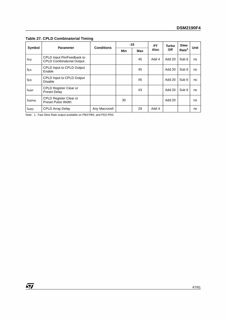
47/61
DSM2190F4
Table 27. CPLD Combinatorial Timing
Note: 1. Fast Slew Rate output available on PB3-PB0, and PD2-PD0.
Symbol Parameter Conditions-15 PT
AlocTurbo
OffSlewRate1 Unit
Min Max
tPDCPLD Input Pin/Feedback to CPLD Combinatorial Output
45 Add 4 Add 20 Sub 6 ns
tEACPLD Input to CPLD Output Enable
45 Add 20 Sub 6 ns
tERCPLD Input to CPLD Output Disable
45 Add 20 Sub 6 ns
tARPCPLD Register Clear or Preset Delay
43 Add 20 Sub 6 ns
tARPWCPLD Register Clear or Preset Pulse Width
30 Add 20 ns
tARD CPLD Array Delay Any Macrocell 29 Add 4 ns
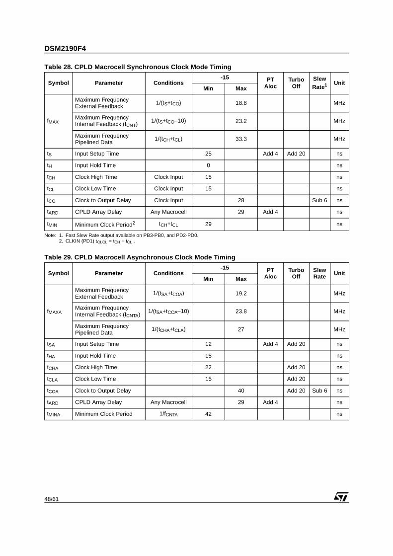
DSM2190F4
48/61
Table 28. CPLD Macrocell Synchronous Clock Mode Timing
Note: 1. Fast Slew Rate output available on PB3-PB0, and PD2-PD0.2. CLKIN (PD1) tCLCL = tCH + tCL .
Table 29. CPLD Macrocell Asynchronous Clock Mode Timing
Symbol Parameter Conditions-15 PT
AlocTurbo
OffSlew Rate1 Unit
Min Max
fMAX
Maximum FrequencyExternal Feedback
1/(tS+tCO) 18.8 MHz
Maximum FrequencyInternal Feedback (fCNT)
1/(tS+tCO–10) 23.2 MHz
Maximum FrequencyPipelined Data
1/(tCH+tCL) 33.3 MHz
tS Input Setup Time 25 Add 4 Add 20 ns
tH Input Hold Time 0 ns
tCH Clock High Time Clock Input 15 ns
tCL Clock Low Time Clock Input 15 ns
tCO Clock to Output Delay Clock Input 28 Sub 6 ns
tARD CPLD Array Delay Any Macrocell 29 Add 4 ns
tMIN Minimum Clock Period2 tCH+tCL 29 ns
Symbol Parameter Conditions-15 PT
AlocTurbo
OffSlewRate Unit
Min Max
fMAXA
Maximum FrequencyExternal Feedback
1/(tSA+tCOA) 19.2 MHz
Maximum FrequencyInternal Feedback (fCNTA)
1/(tSA+tCOA–10) 23.8 MHz
Maximum FrequencyPipelined Data
1/(tCHA+tCLA) 27 MHz
tSA Input Setup Time 12 Add 4 Add 20 ns
tHA Input Hold Time 15 ns
tCHA Clock High Time 22 Add 20 ns
tCLA Clock Low Time 15 Add 20 ns
tCOA Clock to Output Delay 40 Add 20 Sub 6 ns
tARD CPLD Array Delay Any Macrocell 29 Add 4 ns
tMINA Minimum Clock Period 1/fCNTA 42 ns
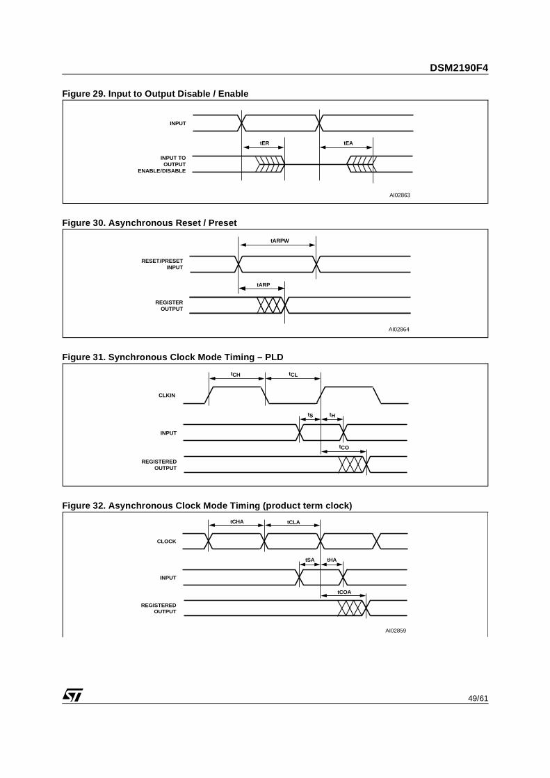
49/61
DSM2190F4
Figure 29. Input to Output Disable / Enable
Figure 30. Asynchronous Reset / Preset
Figure 31. Synchronous Clock Mode Timing – PLD
Figure 32. Asynchronous Clock Mode Timing (product term clock)
tER tEA
INPUT
INPUT TOOUTPUT
ENABLE/DISABLE
AI02863
tARP
REGISTEROUTPUT
tARPW
RESET/PRESETINPUT
AI02864
tCH tCL
tCO
tHtS
CLKIN
INPUT
REGISTEREDOUTPUT
tCHA tCLA
tCOA
tHAtSA
CLOCK
INPUT
REGISTEREDOUTPUT
AI02859
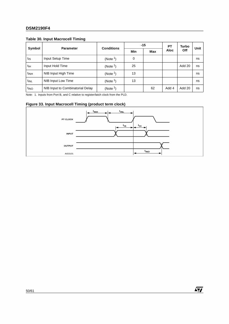
DSM2190F4
50/61
Table 30. Input Macrocell Timing
Note: 1. Inputs from Port B, and C relative to register/latch clock from the PLD.
Figure 33. Input Macrocell Timing (product term clock)
Symbol Parameter Conditions-15 PT
AlocTurbo
Off UnitMin Max
tIS Input Setup Time (Note 1) 0 ns
tIH Input Hold Time (Note 1) 25 Add 20 ns
tINH NIB Input High Time (Note 1) 13 ns
tINL NIB Input Low Time (Note 1) 13 ns
tINO NIB Input to Combinatorial Delay (Note 1) 62 Add 4 Add 20 ns
t INH t INL
t INO
t IHt IS
PT CLOCK
INPUT
OUTPUT
AI03101
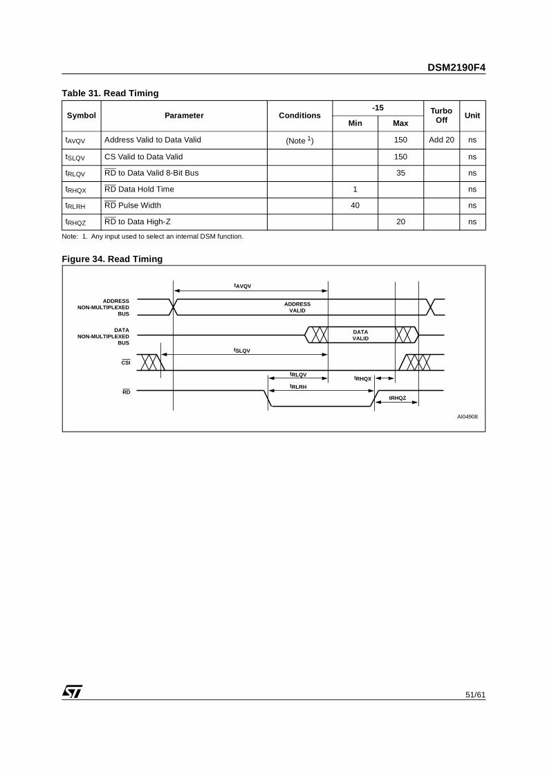
51/61
DSM2190F4
Table 31. Read Timing
Note: 1. Any input used to select an internal DSM function.
Figure 34. Read Timing
Symbol Parameter Conditions-15 Turbo
Off UnitMin Max
tAVQV Address Valid to Data Valid (Note 1) 150 Add 20 ns
tSLQV CS Valid to Data Valid 150 ns
tRLQV RD to Data Valid 8-Bit Bus 35 ns
tRHQX RD Data Hold Time 1 ns
tRLRH RD Pulse Width 40 ns
tRHQZ RD to Data High-Z 20 ns
tAVQV
tSLQV
tRLQV tRHQX
tRHQZ
tRLRH
ADDRESSVALID
DATAVALID
ADDRESSNON-MULTIPLEXED
BUS
DATANON-MULTIPLEXED
BUS
CSI
RD
AI04908
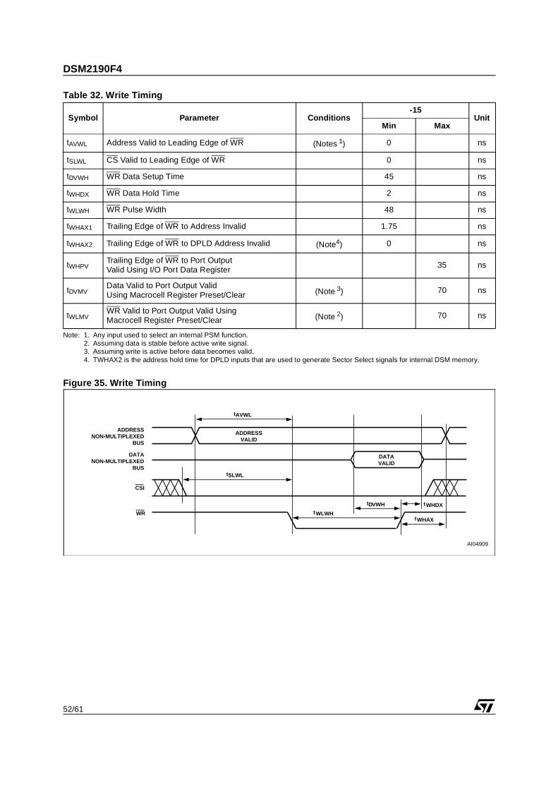
DSM2190F4
52/61
Table 32. Write Timing
Note: 1. Any input used to select an internal PSM function.2. Assuming data is stable before active write signal.3. Assuming write is active before data becomes valid.4. TWHAX2 is the address hold time for DPLD inputs that are used to generate Sector Select signals for internal DSM memory.
Figure 35. Write Timing
Symbol Parameter Conditions-15
UnitMin Max
tAVWL Address Valid to Leading Edge of WR (Notes 1) 0 ns
tSLWL CS Valid to Leading Edge of WR 0 ns
tDVWH WR Data Setup Time 45 ns
tWHDX WR Data Hold Time 2 ns
tWLWH WR Pulse Width 48 ns
tWHAX1 Trailing Edge of WR to Address Invalid 1.75 ns
tWHAX2 Trailing Edge of WR to DPLD Address Invalid (Note4) 0 ns
tWHPVTrailing Edge of WR to Port OutputValid Using I/O Port Data Register
35 ns
tDVMVData Valid to Port Output ValidUsing Macrocell Register Preset/Clear (Note 3) 70 ns
tWLMVWR Valid to Port Output Valid UsingMacrocell Register Preset/Clear (Note 2) 70 ns
tAVWL
tSLWL
t WHDX
t WHAXt WLWH
tDVWH
ADDRESSVALID
DATAVALID
ADDRESSNON-MULTIPLEXED
BUS
DATANON-MULTIPLEXED
BUS
CSI
WR
AI04909
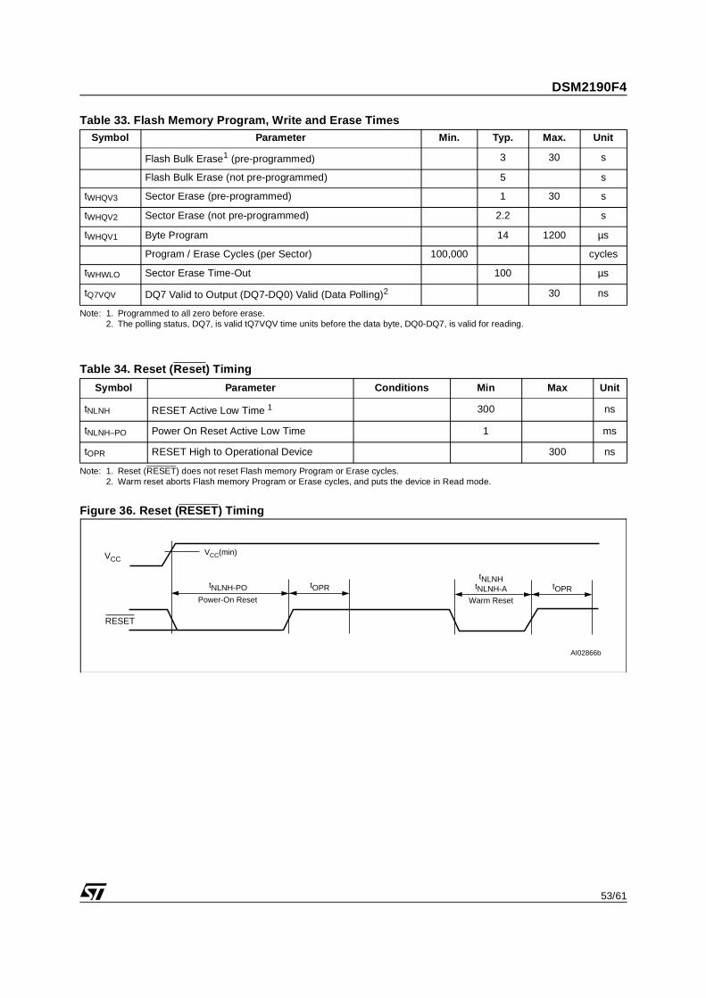
53/61
DSM2190F4
Table 33. Flash Memory Program, Write and Erase Times
Note: 1. Programmed to all zero before erase.2. The polling status, DQ7, is valid tQ7VQV time units before the data byte, DQ0-DQ7, is valid for reading.
Table 34. Reset (Reset) Timing
Note: 1. Reset (RESET) does not reset Flash memory Program or Erase cycles.2. Warm reset aborts Flash memory Program or Erase cycles, and puts the device in Read mode.
Figure 36. Reset (RESET) Timing
Symbol Parameter Min. Typ. Max. Unit
Flash Bulk Erase1 (pre-programmed) 3 30 s
Flash Bulk Erase (not pre-programmed) 5 s
tWHQV3 Sector Erase (pre-programmed) 1 30 s
tWHQV2 Sector Erase (not pre-programmed) 2.2 s
tWHQV1 Byte Program 14 1200 µs
Program / Erase Cycles (per Sector) 100,000 cycles
tWHWLO Sector Erase Time-Out 100 µs
tQ7VQV DQ7 Valid to Output (DQ7-DQ0) Valid (Data Polling)2 30 ns
Symbol Parameter Conditions Min Max Unit
tNLNH RESET Active Low Time 1 300 ns
tNLNH–PO Power On Reset Active Low Time 1 ms
tOPR RESET High to Operational Device 300 ns
tNLNH-PO tOPR
AI02866b
RESET
tNLNHtNLNH-A tOPR
VCCVCC(min)
Power-On Reset Warm Reset
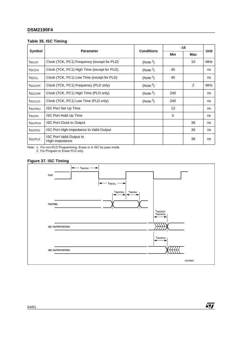
DSM2190F4
54/61
Table 35. ISC Timing
Note: 1. For non-PLD Programming, Erase or in ISC by-pass mode.2. For Program or Erase PLD only.
Figure 37. ISC Timing
Symbol Parameter Conditions-15
UnitMin Max
tISCCF Clock (TCK, PC1) Frequency (except for PLD) (Note 1) 10 MHz
tISCCH Clock (TCK, PC1) High Time (except for PLD) (Note 1) 45 ns
tISCCL Clock (TCK, PC1) Low Time (except for PLD) (Note 1) 45 ns
tISCCFP Clock (TCK, PC1) Frequency (PLD only) (Note 2) 2 MHz
tISCCHP Clock (TCK, PC1) High Time (PLD only) (Note 2) 240 ns
tISCCLP Clock (TCK, PC1) Low Time (PLD only) (Note 2) 240 ns
tISCPSU ISC Port Set Up Time 13 ns
tISCPH ISC Port Hold Up Time 5 ns
tISCPCO ISC Port Clock to Output 36 ns
tISCPZV ISC Port High-Impedance to Valid Output 36 ns
tISCPVZISC Port Valid Output to High-Impedance
36 ns
ISCCH
TCK
TDI/TMS
ISC OUTPUTS/TDO
ISC OUTPUTS/TDO
t
ISCCLt
ISCPHtISCPSUt
ISCPVZt
ISCPZVtISCPCOt
AI02865
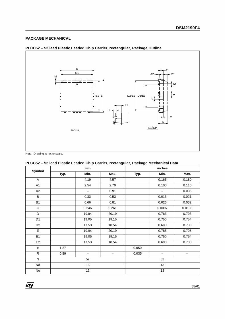
55/61
DSM2190F4
PACKAGE MECHANICAL
PLCC52 – 52 lead Plastic Leaded Chip Carrier, rectangular, Package Outline
Note: Drawing is not to scale.
PLCC52 – 52 lead Plastic Leaded Chip Carrier, rectangular, Package Mechanical Data
Symbolmm inches
Typ. Min. Max. Typ. Min. Max.
A 4.19 4.57 0.165 0.180
A1 2.54 2.79 0.100 0.110
A2 – 0.91 – 0.036
B 0.33 0.53 0.013 0.021
B1 0.66 0.81 0.026 0.032
C 0.246 0.261 0.0097 0.0103
D 19.94 20.19 0.785 0.795
D1 19.05 19.15 0.750 0.754
D2 17.53 18.54 0.690 0.730
E 19.94 20.19 0.785 0.795
E1 19.05 19.15 0.750 0.754
E2 17.53 18.54 0.690 0.730
e 1.27 – – 0.050 – –
R 0.89 – – 0.035 – –
N 52 52
Nd 13 13
Ne 13 13
PLCC-B
D
E1 E
1 N
D1
CP
bD2/E2 e
b1
A1
A
A2
D3/E3
M
L1
L
C
M1
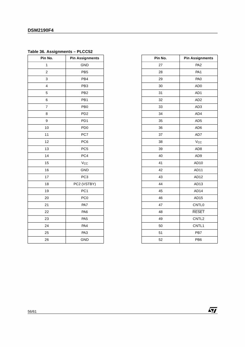
DSM2190F4
56/61
Table 36. Assignments – PLCC52
Pin No. Pin Assignments Pin No. Pin Assignments
1 GND 27 PA2
2 PB5 28 PA1
3 PB4 29 PA0
4 PB3 30 AD0
5 PB2 31 AD1
6 PB1 32 AD2
7 PB0 33 AD3
8 PD2 34 AD4
9 PD1 35 AD5
10 PD0 36 AD6
11 PC7 37 AD7
12 PC6 38 VCC
13 PC5 39 AD8
14 PC4 40 AD9
15 VCC 41 AD10
16 GND 42 AD11
17 PC3 43 AD12
18 PC2 (VSTBY) 44 AD13
19 PC1 45 AD14
20 PC0 46 AD15
21 PA7 47 CNTL0
22 PA6 48 RESET
23 PA5 49 CNTL2
24 PA4 50 CNTL1
25 PA3 51 PB7
26 GND 52 PB6
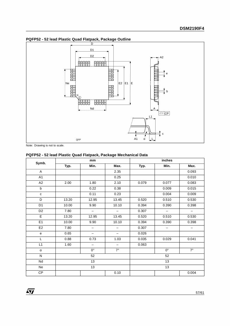
57/61
DSM2190F4
PQFP52 - 52 lead Plastic Quad Flatpack, Package Outline
Note: Drawing is not to scale.
PQFP52 - 52 lead Plastic Quad Flatpack, Package Mechanical Data
Symb.mm inches
Typ. Min. Max. Typ. Min. Max.
A 2.35 0.093
A1 0.25 0.010
A2 2.00 1.80 2.10 0.079 0.077 0.083
b 0.22 0.38 0.009 0.015
c 0.11 0.23 0.004 0.009
D 13.20 12.95 13.45 0.520 0.510 0.530
D1 10.00 9.90 10.10 0.394 0.390 0.398
D2 7.80 – – 0.307 – –
E 13.20 12.95 13.45 0.520 0.510 0.530
E1 10.00 9.90 10.10 0.394 0.390 0.398
E2 7.80 – – 0.307 – –
e 0.65 – – 0.026
L 0.88 0.73 1.03 0.035 0.029 0.041
L1 1.60 – – 0.063
α 0° 7° 0° 7°
N 52 52
Nd 13 13
Ne 13 13
CP 0.10 0.004
QFP
Nd
E1
CP
b
e
A2
A
N
LA1 α
D1
D
1
ENe
c
D2
E2
L1
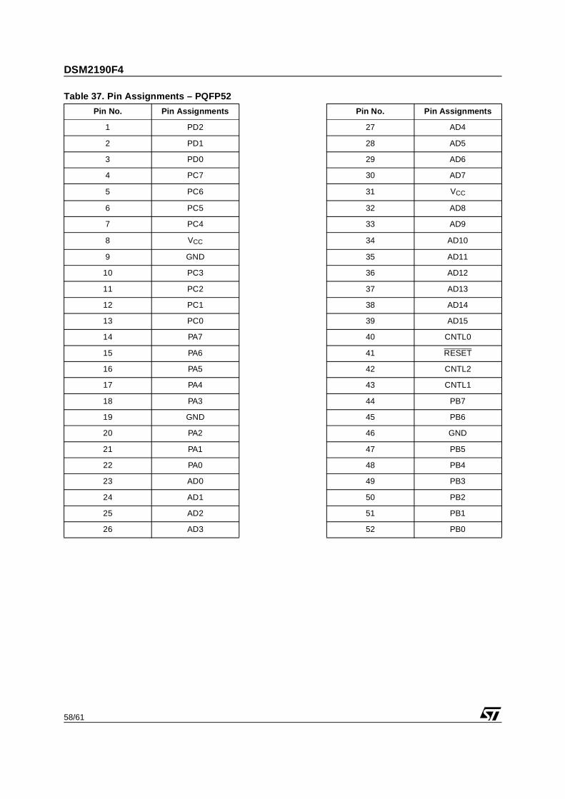
DSM2190F4
58/61
Table 37. Pin Assignments – PQFP52
Pin No. Pin Assignments Pin No. Pin Assignments
1 PD2 27 AD4
2 PD1 28 AD5
3 PD0 29 AD6
4 PC7 30 AD7
5 PC6 31 VCC
6 PC5 32 AD8
7 PC4 33 AD9
8 VCC 34 AD10
9 GND 35 AD11
10 PC3 36 AD12
11 PC2 37 AD13
12 PC1 38 AD14
13 PC0 39 AD15
14 PA7 40 CNTL0
15 PA6 41 RESET
16 PA5 42 CNTL2
17 PA4 43 CNTL1
18 PA3 44 PB7
19 GND 45 PB6
20 PA2 46 GND
21 PA1 47 PB5
22 PA0 48 PB4
23 AD0 49 PB3
24 AD1 50 PB2
25 AD2 51 PB1
26 AD3 52 PB0
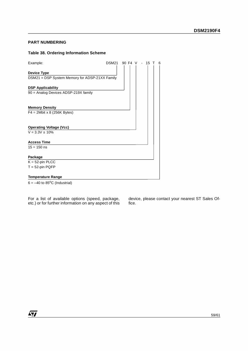
59/61
DSM2190F4
PART NUMBERING
Table 38. Ordering Information Scheme
For a list of available options (speed, package,etc.) or for further information on any aspect of this
device, please contact your nearest ST Sales Of-fice.
Example: DSM21 90 F4 V - 15 T 6
Device TypeDSM21 = DSP System Memory for ADSP-21XX Family
DSP Applicability90 = Analog Devices ADSP-219X family
Memory DensityF4 = 2Mbit x 8 (256K Bytes)
Operating Voltage (Vcc)V = 3.3V ± 10%
Access Time15 = 150 ns
PackageK = 52-pin PLCCT = 52-pin PQFP
Temperature Range
6 = –40 to 85oC (Industrial)

DSM2190F4
60/61
REVISION HISTORY
Table 39. Document Revision History
Date Rev. Description of Revision
27-Aug-2001 1.0 Document written
06-Nov-2001 1.1 Document released
17-Dec-2001 1.2 PQFP52 package mechanical data updated
18-Sep-2002 1.3 JTAG Debug bus separated from JTAG ISP bus

61/61
DSM2190F4
Information furnished is believed to be accurate and reliable. However, STMicroelectronics assumes no responsibility for the consequencesof use of such information nor for any infringement of patents or other rights of third parties which may result from its use. No license is grantedby implication or otherwise under any patent or patent rights of STMicroelectronics. Specifications mentioned in this publication are subjectto change without notice. This publication supersedes and replaces all information previously supplied. STMicroelectronics products are notauthorized for use as critical components in life support devices or systems without express written approval of STMicroelectronics.
The ST logo is registered trademark of STMicroelectronics
All other names are the property of their respective owners
© 2002 STMicroelectronics - All Rights Reserved
STMicroelectronics group of companies
Australia - Brazil - Canada - China - Finland - France - Germany - Hong Kong -
India - Israel - Italy - Japan - Malaysia - Malta - Morocco - Singapore - Spain - Sweden - Switzerland - United Kingdom - United States.
www.st.com