Flexible Organic Tribotronic Transistor Memory for a ... · Flexible Organic Tribotronic Transistor...
5
© 2015 WILEY-VCH Verlag GmbH & Co. KGaA, Weinheim 1 wileyonlinelibrary.com COMMUNICATION Flexible Organic Tribotronic Transistor Memory for a Visible and Wearable Touch Monitoring System Jing Li, Chi Zhang, Lian Duan, Li Min Zhang, Li Duo Wang, Gui Fang Dong,* and Zhong Lin Wang* J. Li, Prof. L. Duan, Prof. L. D. Wang, Prof. G. F. Dong Key Laboratory of Organic Optoelectronics and Molecular Engineering of Ministry of Education Chemistry Department Tsinghua University Beijing 100084, China E-mail: [email protected] Prof. C. Zhang, L. M. Zhang, Prof. Z. L. Wang Beijing Institute of Nanoenergy and Nanosystems Chinese Academy of Sciences Beijing 100083, China E-mail: [email protected] Prof. Z. L. Wang School of Material Science and Engineering Georgia Institute of Technology Atlanta, GA 30332-0245, USA DOI: 10.1002/adma.201504424 been successfully fabricated on polyethylene terephthalate (PET) substrates with high flexibility and the retention time of the signals exceeds 10 2 s. By further coupling with a flexible organic light-emitting diode (OLED), a visible and wearable touch monitoring system is achieved, in which touch trig- gering can be memorized and shown as the emission from the OLED based on tris-(8-hydroxyquinoline) aluminum (Alq 3 ). This system has potential applications in security monitoring, mechanical imaging, and intelligent control systems. Figure 1a depicts the sketch of the touch monitoring system, which mainly includes an OTTM and an OLED as schemati- cally illustrated in Figure 1b. The OTTM is composed of the TENG with a structure of copper/PVC/copper as a triggering- input and reset unit, and the OTM on top of the TENG as a storage unit to record the detected triggering from the TENG. In the OTM, a Ta 2 O 5 layer was formed on the bottom indium tin oxide (ITO) gate electrode. A 2 nm thick separated Ta floating gate layer was sandwiched between two polymethyl methacrylate (PMMA) layers, which were fabricated on the Ta 2 O 5 layer. A pentacene film with the thickness of 45 nm was used as the semiconductor layer, with Au drain and source elec- trodes on it. The OLED with a structure ITO/ N, N′-diphenyl- N, N′ -bis(1,1′ -biphenyl)-4,4′ -diamine(NPB)/Alq 3 /Mg:Ag/Ag acts as a touch signal-output functional unit. A double pole double throw (DPDT) switch is employed to transfer the system between the monitoring and resetting modes. In the moni- toring mode, the DPDT is linked to No. 1 and 2 terminals, con- necting the anode and cathode of the TENG with the gate and source electrodes of the OTM, respectively. In this case, touch on the TENG is an input action and will cause the writing pro- cedure for the OTTM. On the contrary, in the resetting mode, the DPDT is connected to No. 1′ and 2′ terminals and the cathode and anode of the TENG are connected to the gate and source electrodes of the OTM, respectively. In that case, touch on the TENG is a reset action and will trigger the erasing proce- dure for the OTTM. Figure 1c presents a practical application of the system and the working procedures of the touch monitoring system are played in the supporting videos (Video S1, Supporting Informa- tion, is the monitoring mode and Video S2, Supporting Infor- mation, is the resetting mode). The OTTM is placed inside a classified document to detect and record the touch actions and the OLED is worn on a person’s wrist for monitoring. A voltage ( V DS ) of −8 V is applied to the drain electrode of the OTTM during the whole period. In the monitoring mode, the device is in the OFF state with no touch action, and the drain cur- rent below 10 −10 A is too low to enlighten the OLED. Once an external touch on the OTTM results in the ON state, the action Organic electronic devices are unique owing to their advantages in terms of flexibility, wearability, and biological histocompat- ibility. [1–5] As a key component, organic transistor memory (OTM) integrates switching capacity and memory in a single device, arousing great interests for its scientific and techno- logical significance. [6,7] Commonly, OTMs record electrical signals by gate voltage programming and erasing. [6–10] Some- times, OTMs also memorize light signals by using highly photosensitive semiconductors, such asorganic phototransistor memory. [11,12] We have developed a type of photoassistant elec- trical-programming OTM by introducing a high- k dielectric material with photosensitive semiconductor. [13,14] These OTMs can record both light and electrical signals and achieve multibit memories. Recently, triboelectric nanogenerator (TENG) has been invented as a novel device for converting ambient mechanical energy into electricity, [15–19] which has also been used as the triboelectric-charge-controlled source [20–22] and providing a promising alternative approach to control electronics for a new field of tribotronics. [23–26] As the electrostatic potential created by TENG can be used as a gate voltage to control transistor, it can be also employed for OTM in place of the traditional gate voltage programming and erasing, which can realize an active memory system for external touch actions. Here in this work, a new type of flexible organic tribotronic transistor memory (OTTM) has been developed by coupling a TENG and an OTM. Different from traditional OTMs con- trolled by electric signals of gate voltages, the OTTM can be written and erased by externally applied touch actions as an active memory. The high-performance Ta 2 O 5 /pentacene-based OTM and polyvinyl chloride (PVC)/copper-based TENG have Adv. Mater. 2015, DOI: 10.1002/adma.201504424 www.advmat.de www.MaterialsViews.com
Transcript of Flexible Organic Tribotronic Transistor Memory for a ... · Flexible Organic Tribotronic Transistor...

© 2015 WILEY-VCH Verlag GmbH & Co. KGaA, Weinheim 1wileyonlinelibrary.com
CO
MM
UN
ICATIO
N
Flexible Organic Tribotronic Transistor Memory for a Visible and Wearable Touch Monitoring System
Jing Li , Chi Zhang , Lian Duan , Li Min Zhang , Li Duo Wang , Gui Fang Dong ,* and Zhong Lin Wang *
J. Li, Prof. L. Duan, Prof. L. D. Wang, Prof. G. F. Dong Key Laboratory of Organic Optoelectronics and Molecular Engineering of Ministry of Education Chemistry Department Tsinghua University Beijing 100084 , China E-mail: [email protected] Prof. C. Zhang, L. M. Zhang, Prof. Z. L. Wang Beijing Institute of Nanoenergy and Nanosystems Chinese Academy of Sciences Beijing 100083 , China E-mail: [email protected] Prof. Z. L. Wang School of Material Science and Engineering Georgia Institute of Technology Atlanta , GA 30332-0245 , USA
DOI: 10.1002/adma.201504424
been successfully fabricated on polyethylene terephthalate (PET) substrates with high fl exibility and the retention time of the signals exceeds 10 2 s. By further coupling with a fl exible organic light-emitting diode (OLED), a visible and wearable touch monitoring system is achieved, in which touch trig-gering can be memorized and shown as the emission from the OLED based on tris-(8-hydroxyquinoline) aluminum (Alq 3 ). This system has potential applications in security monitoring, mechanical imaging, and intelligent control systems.
Figure 1 a depicts the sketch of the touch monitoring system, which mainly includes an OTTM and an OLED as schemati-cally illustrated in Figure 1 b. The OTTM is composed of the TENG with a structure of copper/PVC/copper as a triggering-input and reset unit, and the OTM on top of the TENG as a storage unit to record the detected triggering from the TENG. In the OTM, a Ta 2 O 5 layer was formed on the bottom indium tin oxide (ITO) gate electrode. A 2 nm thick separated Ta fl oating gate layer was sandwiched between two polymethyl methacrylate (PMMA) layers, which were fabricated on the Ta 2 O 5 layer. A pentacene fi lm with the thickness of 45 nm was used as the semiconductor layer, with Au drain and source elec-trodes on it. The OLED with a structure ITO/ N , N ′-diphenyl- N , N ′-bis(1,1′-biphenyl)-4,4′-diamine(NPB)/Alq 3 /Mg:Ag/Ag acts as a touch signal-output functional unit. A double pole double throw (DPDT) switch is employed to transfer the system between the monitoring and resetting modes. In the moni-toring mode, the DPDT is linked to No. 1 and 2 terminals, con-necting the anode and cathode of the TENG with the gate and source electrodes of the OTM, respectively. In this case, touch on the TENG is an input action and will cause the writing pro-cedure for the OTTM. On the contrary, in the resetting mode, the DPDT is connected to No. 1′ and 2′ terminals and the cathode and anode of the TENG are connected to the gate and source electrodes of the OTM, respectively. In that case, touch on the TENG is a reset action and will trigger the erasing proce-dure for the OTTM.
Figure 1 c presents a practical application of the system and the working procedures of the touch monitoring system are played in the supporting videos (Video S1, Supporting Informa-tion, is the monitoring mode and Video S2, Supporting Infor-mation, is the resetting mode). The OTTM is placed inside a classifi ed document to detect and record the touch actions and the OLED is worn on a person’s wrist for monitoring. A voltage ( V DS ) of −8 V is applied to the drain electrode of the OTTM during the whole period. In the monitoring mode, the device is in the OFF state with no touch action, and the drain cur-rent below 10 −10 A is too low to enlighten the OLED. Once an external touch on the OTTM results in the ON state, the action
Organic electronic devices are unique owing to their advantages in terms of fl exibility, wearability, and biological histocompat-ibility. [ 1–5 ] As a key component, organic transistor memory (OTM) integrates switching capacity and memory in a single device, arousing great interests for its scientifi c and techno-logical signifi cance. [ 6,7 ] Commonly, OTMs record electrical signals by gate voltage programming and erasing. [ 6–10 ] Some-times, OTMs also memorize light signals by using highly photosensitive semiconductors, such asorganic phototransistor memory. [ 11,12 ] We have developed a type of photoassistant elec-trical-programming OTM by introducing a high- k dielectric material with photosensitive semiconductor. [ 13,14 ] These OTMs can record both light and electrical signals and achieve multibit memories.
Recently, triboelectric nanogenerator (TENG) has been invented as a novel device for converting ambient mechanical energy into electricity, [ 15–19 ] which has also been used as the triboelectric-charge-controlled source [ 20–22 ] and providing a promising alternative approach to control electronics for a new fi eld of tribotronics. [ 23–26 ] As the electrostatic potential created by TENG can be used as a gate voltage to control transistor, it can be also employed for OTM in place of the traditional gate voltage programming and erasing, which can realize an active memory system for external touch actions.
Here in this work, a new type of fl exible organic tribotronic transistor memory (OTTM) has been developed by coupling a TENG and an OTM. Different from traditional OTMs con-trolled by electric signals of gate voltages, the OTTM can be written and erased by externally applied touch actions as an active memory. The high-performance Ta 2 O 5 /pentacene-based OTM and polyvinyl chloride (PVC)/copper-based TENG have
Adv. Mater. 2015, DOI: 10.1002/adma.201504424
www.advmat.dewww.MaterialsViews.com

2 wileyonlinelibrary.com © 2015 WILEY-VCH Verlag GmbH & Co. KGaA, Weinheim
CO
MM
UN
ICATI
ON
will be recorded and increase the drain current to enlighten the OLED for a warning. With the recorded touch action, the OLED can continuously generate light during the signal retention time (Video S1, Supporting Information). While in the reset-ting mode, a touch on the OTTM is used to erase the recorded signal and reset the system to the OFF state, in which the drain current is decreased and the OLED is turned off (Video S2, Supporting Information). As shown in the supporting videos, a tiny touch force of about 1.5 N is enough to write and reset the OTTM.
Herein, the working mechanism of the OTTM is suggested as follows ( Figure 2 and 3 ). The TENG is fi rst set to the “original
state” with net positive charges on the bottom Cu fi lm and net negative charges on the PVC fi lm before integrated with the OTM (details can be found in Figure S1, Supporting Informa-tion). In the original state of the monitoring mode (Figure 2 a), the mobile PVC/Cu/PET layers are separated from the top Cu fi lm and the gate voltage of the OTM is zero at this moment. In Figure 2 b, external applied touch on the device brings the top Cu and PVC fi lms into contact with each other. For the elec-trostatic induction, electrons fl ow from the ITO gate electrode to the bottom Cu fi lm, leaving net positive charges on the ITO fi lm. Meanwhile, equal numbers of electrons fl ow from the top Cu fi lm to the Au source electrode, resulting in a positive
Adv. Mater. 2015, DOI: 10.1002/adma.201504424
www.advmat.dewww.MaterialsViews.com
Figure 1. Description of the touch monitoring system. a) Schematics of the system. b) Sketch of the OTTM and the OLED. c) Photographs of the system for practical application.
Figure 2. Schematic representations of OTTM operation in monitoring mode. a) The original state without external touch in monitoring mode. b) External touch brings top Cu fi lm and PVC fi lm into contact, causing the writing procedure of the OTTM that the electrons are trapped in Ta fl oating gates from the pentacene fi lm. c) Withdrawal of the touch causes a separation, returning the gate voltage to 0 V, but electrons remain trapped in Ta fl oating gates.
3wileyonlinelibrary.com© 2015 WILEY-VCH Verlag GmbH & Co. KGaA, Weinheim
CO
MM
UN
ICATIO
N
gate voltage is applied on the OTM in this state. With the help of the positive electric fi eld, electrons in the pentacene fi lm are injected to the unoccupied states of the Ta nanoparticles through the PMMA layer, leaving the mobile holes in the pen-tacene fi lm, which can open the conducting channel and lead to the ON state. [ 10 ] When the touch is released, electrons on the bottom Cu layer and source electrode will fl ow back to the ITO fi lm and top Cu layer, respectively, returning the gate voltage to 0 V (Figure 2 c). Because the electrons can stay on the Ta fl oating gate for a certain time, the device remains in the ON state and the external touch action is memorized. To reset the system, the connections of the top and bottom Cu fi lms are switched to the ITO fi lm and the source electrode, respectively (Figure 3 a), with the DPDT described in Figure 1 a (for the sake of simplicity, the DPDT is not shown in Figure 2 and Figure 3 ).
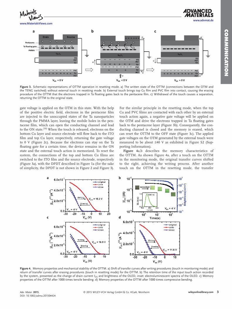
For the similar principle in the resetting mode, when the top Cu and PVC fi lms are contacted with each other by an external touch action again, a negative gate voltage will be applied on the OTM and drive the electrons trapped in Ta fl oating gates back to the pentacene layer (Figure 3 b). Consequently, the con-ducting channel is closed and the memory is erased, which can reset the OTTM to the OFF state (Figure 3 c). The applied gate voltages on the OTM generated by the external touch were measured to be about ±40 V as exhibited in Figure S2 (Sup-porting Information).
Figure 4 a,b describes the memory characteristics of the OTTM. As shown Figure 4 a, after a touch on the OTTM in the monitoring mode, the original transfer curves shifted to the right, achieving the writing process. After another touch on the OTTM in the resetting mode, the transfer
Adv. Mater. 2015, DOI: 10.1002/adma.201504424
www.advmat.dewww.MaterialsViews.com
Figure 3. Schematic representations of OTTM operation in resetting mode. a) The written state of the OTTM (connections between the OTM and the TENG switched) without external touch in resetting mode. b) External touch brings top Cu fi lm and PVC fi lm into contact, causing the erasing procedure of the OTTM that the electrons trapped in Ta fl oating gates back to the pentacene fi lm. c) Withdrawal of the touch causes a separation, returning the OTTM to the original state.
Figure 4. Memory properties and mechanical stability of the OTTM. a) Shift of transfer curves after writing procedures (touch in monitoring mode) and return of transfer curves after erasing procedures (touch in resetting mode) for the OTTM. b) The retention time of the input touch action recorded by the system, presented as the change of drain current I DS and brightness of the OLED, inset: electroluminescent spectra of the OLED. c) Memory properties of the OTTM after 1000 times tensile bending. d) Memory properties of the OTTM after 1000 times compressive bending.

4 wileyonlinelibrary.com © 2015 WILEY-VCH Verlag GmbH & Co. KGaA, Weinheim
CO
MM
UN
ICATI
ON curve returned to the left to achieve the erasing process. It
is noteworthy that the writing and erasing time of the OTM by electrical voltages can be as short as 5 ms (Figure S3, Sup-porting Information), which is favorable for applications in fl ash memories. [ 27,28 ] It indicates that the OTTM has poten-tial to be written and erased by instantaneous mechanical pulses, and the external touch in the experiment as quick as hundreds of milliseconds is enough long for practical applica-tions of the OTTM (Figure S2, Supporting Information). The memory window ( V MW ), defi ned as the shift of V T from the transfer curve at the OFF state (erased) to that at the ON state (written), was 16.3 ± 0.4 V. The ON/OFF ratio (the ratio of I DS at ON state and OFF state when V GS = 0 V and V DS = −8 V) was over 10 5 . The retention time ( T R ), defi ned as the time the stored information dropped to a certain value (1 µA) at which a verifi able error is detected from any cause, [ 29 ] exceeded 10 2 s. The retention time here could also be described as the length of emission from the OLED after the writing procedure. From photographs taken during the reading process, the emission was still visible after 10 2 s. The OLED gave out green emis-sion at a peak of 520 nm (shown inset in Figure 4 b). Although the retention time would be over 10 5 s if defi ned as the time for the ON/OFF currents approaching each other (Figure S4, Supporting Information), which has been generally used in the published works of organic fl oating gate memories, [ 30,31 ] it was still limited and remained to be increased in our further research.
It is worth mentioning that as compared to Au nanoparticles, which are usually used in fl oating gate transistor memories, the Ta fl oating gate used here attracts electrons more strongly, benefi tting for the memory properties. Also, the use of Ta as fl oating gate instead of Au or other nanoparticles simplifi es the device fabrication process. [ 32 ]
The mechanical stability of the OTTM was evaluated through systematic bending tests. As shown in Figure 4 c,d, the memories properties of the OTTM remained almost the same as the initial state after 1000 iterations of compressive or tensile bending. The changeless transfer curves prove that the OTTM has good mechanical stability. The decrease of memory window for the OTTM after compressive bending (from 16.3 to 11.6 V) was due to the enhancement of leakage current as a result of the reduced distance between the Ta fl oating gates, which could be recovered by applying slight tensile stress on the device.
Another criterion for application is the time stability of the device. The memory properties of the OTTM remained steady for at least 2 months, as shown in Figure S5 (Supporting Infor-mation). The memory window ( V MW ) was 12.2 V (75% of the original 16.3 V, the slight degeneration might be caused by the oxygen and water in air) and the retention time ( T R ) still exceeded 10 2 s with the ON/OFF ratio over 10 5 .
The transistor characteristics of the OTM were tested. Figure S6a,b (Supporting Information) is output and transfer curves of the OTM. The fi eld-effect mobility ( µ ) extracted from the saturated region of the transfer curve was 0.29 ± 0.06 cm 2 V −1 s −1 . The dielectric constant ( ε ) of the dielec-tric fi lm, which was used to extract the mobility, was calculated to be 17.5 from the measured capacitance−area line of the ITO/Ta 2 O 5 /PMMA/Ta/PMMA/Au structure (Figure S7, Supporting
Information). The on/off current ratio ( I on/off ) of the OTM reached 10 6 .
We fabricated similar devices on ITO glass substrates to compare with the fl exible devices (Figure S8 and Table S1, Sup-porting Information). The results indicated that both devices have the same characteristics, proving the high quality of the fl exible device.
In conclusion, a visible and wearable touch monitoring system based on the fl exible OTTM and OLED has been suc-cessfully developed. Unlike traditional OTMs, the writing and erasing signals of the OTTM are the external mechanical touches. The fl exible memory exhibited good performance with high electromechanical coupling and memory properties. Fur-thermore, it was demonstrated to have outstanding mechanical and time stability. This work not only introduces a novel kind of tribotronic transistor memory device but also establishes a vis-ible and wearable touch monitoring system for practical appli-cation, in which touch actions could be memorized and shown as the emission from the OLED. This work demonstrates the great potential of organic optoelectronics and tribophototronics for intelligent functional instruments and human-computer interaction techniques.
Experimental Section Fabrication of OTTM : First, two pieces of PET substrates were cleaned
and cut as substrates. A layer of 100 nm copper was sputtered on the top PET substrate with 150 nm ITO fi lm on the back. Then, coated with 100 nm copper, a layer of PVC with the thickness of 100 µm was assembled on the bottom PET substrate with the PVC facing the copper on the top substrate. An OTM was fabricated on the top of the TENG as followings. A 300 nm Ta 2 O 5 gate dielectric fi lm was sputtered in an Ar/O 2 (7:3) gas mixture with a 101.6 mm (diameter) × 7 mm target material Ta (General Research Institute for Nonferrous Metals, >99.9%) on the ITO fi lm as gate electrode. A PMMA fi lm (20 mg mL −1 in CH 2 Cl 2 ) with thickness of 20 nm was deposited on the Ta 2 O 5 fi lm by spin coating at 1500 rpm. The fi lm was annealed at 70 °C for 1 h. Then, 2 nm separated Ta was sputtered on it to form fl oating gate using a shadow mask, followed by spin coating of another 20 nm PMMA fi lm. After that, a 45 nm pentacene (Sigma-Aldrich, >99%, used as received) fi lm was thermally evaporated at a deposition rate of 0.01−0.02 nm s −1 under a 1 × 10 −4 Pa vacuum. Finally, source and drain gold electrodes were deposited through shadow masks. The channel length ( L ) and width ( W ) were 60 and 1000 µm, respectively. The OTM was integrated with the TENG as the OTTM.
Fabrication of OLED : First, a NPB fi lm with a thickness of 50 nm was formed on substrate with ITO on it by vacuum deposition, the deposition rate was 0.1−0.2 nm s −1 . Second, a 50 nm thick tris-(8-hydroxyquinoline) aluminum (Alq 3 ) fi lm was deposited at a deposition rate of 0.1 nm s −1 . Then an Mg–Ag (10:1) fi lm (50 nm) was fabricated, followed by deposition of a pure Ag fi lm (150 nm) at a deposition rate of 0.1−0.2 nm s −1 to fi nish the fabrication of an OLED.
Characterization : The capacitance per area ( C i ) of gate dielectrics was obtained by measuring capacitance−frequency properties of ITO/Ta 2 O 5 /PMMA/Ta/PMMA/Au with an Agilent 4294A analyzer. The OTTM performance was measured by a Keithley 4200 semiconductor characterization system in air at room temperature.
Supporting Information Supporting Information is available from the Wiley Online Library or from the author.
Adv. Mater. 2015, DOI: 10.1002/adma.201504424
www.advmat.dewww.MaterialsViews.com

5wileyonlinelibrary.com© 2015 WILEY-VCH Verlag GmbH & Co. KGaA, Weinheim
CO
MM
UN
ICATIO
N
Adv. Mater. 2015, DOI: 10.1002/adma.201504424
www.advmat.dewww.MaterialsViews.com
Acknowledgements J.L. and C.Z. contributed equally to this work. This work was supported by the National Natural Science Foundation of China (Grant Nos. 61177023, 61474069, and 51173096), and the Youth Innovation Promotion Association, CAS. The authors thank H. Y. Zhao, W. H. Li, and D. Li for assistance with the preparation of the supporting videos.
Received: September 9, 2015 Revised: September 27, 2015
Published online:
[1] S. Liu , W. M. Wang , A. L. Briseno , S. C. B. Mannsfeld , Z. Bao , Adv. Mater. 2009 , 21 , 1217 .
[2] M. Ramuz , B. C. Tee , J. B. Tok , Z. Bao , Adv. Mater. 2012 , 24 , 3223 . [3] Y. Zhao , C. Di , X. Gao , Y. Hu , Y. Guo , L. Zhang , Y. Liu , J. Wang ,
W. Hu , D. Zhu , Adv. Mater. 2011 , 23 , 3448 . [4] Y. Zang , F. Zhang , D. Huang , X. Gao , C. A. Di , D. Zhu , Nat.
Commun. 2015 , 6 , 6269 . [5] Y. Yang , R. C. da Costa , M. J. Fuchter , A. J. Campbell , Nat. Photon.
2013 , 7 , 634 . [6] Y. Guo , G. Yu , Y. Liu , Adv. Mater. 2010 , 22 , 4427 . [7] C. Di , F. Zhang , D. Zhu , Adv. Mater. 2013 , 25 , 313 . [8] T. Sekitani , T. Yokota , U. Zschieschang , H. Klauk , S. Bauer ,
K. Takeuchi , M. Takamiya , T. Sakurai , T. Someya , Science 2009 , 326 , 1516 .
[9] P. Heremans , G. H. Gelinck , R. Müller , K. Baeg , D. Kim , Y. Noh , Chem. Mater. 2011 , 23 , 341 .
[10] X. She , C. Liu , Q. Sun , X. Gao , S. Wang , Org. Electron. 2012 , 13 , 1908 .
[11] Y. Guo , C. Di , S. Ye , X. Sun , J. Zheng , Y. Wen , W. Wu , G. Yu , Y. Liu , Adv. Mater. 2009 , 21 , 1954 .
[12] L. Zhang , T. Wu , Y. Guo , Y. Zhao , X. Sun , Y. Wen , G. Yu , Y. Liu , Sci. Rep. 2013 , 3 , 1080 .
[13] X. Liu , H. Zhao , G. Dong , L. Duan , D. Li , L. Wang , Y. Qiu , ACS Appl. Mater. Interfaces 2014 , 6 , 8337 .
[14] X. Liu , G. Dong , D. Zhao , Y. Wang , L. Duan , L. Wang , Y. Qiu , Org. Electron. 2012 , 13 , 2917 .
[15] F. Fan , Z. Tian , Z. L. Wang , Nano Energy 2012 , 1 , 328 . [16] Z. L. Wang , J. Chen , L. Lin , Energy Environ. Sci. 2015 , 8 , 2250 . [17] Z. L. Wang , Faraday Discuss. 2014 , 176 , 447 . [18] C. Zhang , W. Tang , C. Han , F. Fan , Z. L. Wang , Adv. Mater. 2014 , 26 ,
3580 . [19] C. Zhang , T. Zhou , W. Tang , C. Han , L. Zhang , Z. L. Wang , Adv.
Energy Mater. 2014 , 4 , 1301798 . [20] C. Zhang , W. Tang , Y. Pang , C. Han , Z. L. Wang , Adv. Mater. 2015 ,
27 , 719 . [21] C. B. Han , C. Zhang , J. Tian , X. Li , L. Zhang , Z. Li , Z. L. Wang , Nano
Res. 2014 , 8 , 219 . [22] X. Chen , M. Iwamoto , Z. Shi , L. Zhang , Z. L. Wang , Adv. Funct.
Mater. 2015 , 25 , 739 . [23] C. Zhang , W. Tang , L. Zhang , C. Han , Z. L. Wang , ACS Nano 2014 ,
8 , 8702 . [24] C. Zhang , L. M. Zhang , W. Tang , C. B. Han , Z. L. Wang , Adv. Mater.
2015 , 27 , 3533 . [25] C. Zhang , J. Li , C. B. Han , L. M. Zhang , X. Y. Chen , L. D. Wang ,
G. F. Dong , Z. L. Wang , Adv. Funct. Mater. 2015 , 25 , 5625. [26] Y. Liu , S. Niu , Z. L. Wang , Adv. Electron. Mater. 2015 , 1 , 1500124 . [27] W. L. Leong , N. Mathews , B. Tan , S. Vaidyanathan , F. Dötz ,
S. Mhaisalkar , J. Mater. Chem. 2011 , 21 , 5203 . [28] J. H. Park , C. W. Byun , K. H. Seok , H. Y. Kim , H. J. Chae , S. K. Lee ,
S. W. Son , D. Ahn , S. K. Joo , J. Appl. Phys. 2014 , 116 , 124512 . [29] IEEE Standard for Defi nitions, Symbols, and Characterization of
Floating Gate Memory Arrays , IEEE, Piscataway, NJ, USA 1999 . [30] C. Tseng , D. Huang , Y. Tao , ACS Appl. Mater. Interfaces 2013 , 5 ,
9528 . [31] M. Kang , K. Baeg , D. Khim , Y. Noh , D. Kim , Adv. Funct. Mater. 2013 ,
23 , 3503 . [32] Y. S. Park , J. S. Lee , Adv. Mater. 2015 , 27 , 706 .