flexible nico2o4 SI 160308 Ananth Supplementary Information Realization of High Performance Flexible...
24
1 Supplementary Information Realization of High Performance Flexible Wire Supercapacitors Based on 3-Dimensional NiCo 2 O 4 /Ni Fibers Ananthakumar Ramadoss 1 , Kyeong-Nam Kang 2 , Hyo-Jin Ahn 2 , Sun-I Kim 2 , Seung-Tak Ryu *1 , and Ji-Hyun Jang *2 1 Mixed Signal Integrated Circuit Lab, School of Electrical Engineering, Korea Advanced Institute of Science and Technology, Daejeon 305-701, Republic of Korea 2 School of Energy and Chemical Engineering, Low Dimensional Carbon Materials Center, Ulsan National Institute of Science and Technology, Ulsan 689-798, Republic of Korea ………………………………………………………………………………………… *Corresponding author: Fax: 82-52-217-3008; Tel: 82-52-217-2922 Email: [email protected] (Ji-Hyun Jang) & [email protected] (Seung-Tak Ryu) Electronic Supplementary Material (ESI) for Journal of Materials Chemistry A. This journal is © The Royal Society of Chemistry 2016
Transcript of flexible nico2o4 SI 160308 Ananth Supplementary Information Realization of High Performance Flexible...

1
Supplementary Information
Realization of High Performance Flexible Wire Supercapacitors Based on 3-Dimensional NiCo2O4/Ni Fibers
Ananthakumar Ramadoss1, Kyeong-Nam Kang2, Hyo-Jin Ahn2, Sun-I Kim2,
Seung-Tak Ryu*1, and Ji-Hyun Jang *2
1Mixed Signal Integrated Circuit Lab, School of Electrical Engineering, Korea Advanced
Institute of Science and Technology, Daejeon 305-701, Republic of Korea
2School of Energy and Chemical Engineering, Low Dimensional Carbon Materials Center, Ulsan National Institute of Science and Technology, Ulsan 689-798, Republic of Korea
…………………………………………………………………………………………
*Corresponding author: Fax: 82-52-217-3008; Tel: 82-52-217-2922
Email: [email protected] (Ji-Hyun Jang) & [email protected] (Seung-Tak Ryu)
Electronic Supplementary Material (ESI) for Journal of Materials Chemistry A.This journal is © The Royal Society of Chemistry 2016
2
A. Materials
All the chemicals used in our experiments were of analytical grade and were directly
used without further purification. The nickel (Ni) wire (0.5 mm), nickel chloride (NiCl4),
ammonium chloride (NH4Cl), cobalt nitrate (Co(NO3)2), nickel nitrate (Ni(NO3)2), polyvinyl
alcohol (PVA), titanium(IV) chloride (TiCl4), fluorine doped tin oxide substrate, chloroplatinic
acid (H2PtCl6), isopropyl alcohol, 1-hexyl-2,3-dimethylimidazolium iodide (99.9%, C-tri),
iodine, 4-tert-buthylpyridine, and lithium iodide in acetonitrile were obtained from Sigma
Aldrich, Korea. Potassium hydroxide (KOH) and hydrochloric acid (HCl) were purchased from
Samchun Pure Chemical Co. Ltd. Korea. TiO2 paste purchased from ENB Korea Co. Ltd. Ultra-
pure (De-ionized) water was used for all experiments.
3
B. Experimental section
Preparation of 3D-Ni on Ni-wire
The 3D-Ni on Ni-wire was electrodeposited by a hydrogen bubble template method 1,
2. Briefly, the Ni-wire was first etched in HCl to remove the oxide layer followed by complete
washing with DI water and ethanol, and the Ni-wire was then used as the cathode for
constructing the 3D-Ni. A platinum mesh was used as an anode (current collector), keeping the
distance between the two electrodes at 1 cm. The 3D-Ni was then electrodeposited using
hydrogen bubbles as templates on the nickel wire at a constant current of 2.5 A for 60 s using
a regulated DC power supply LP-3010 with the electrolyte containing 0.1 M NiCl2 and 2 M
NH4Cl at a pH of 3.5. After the deposition, the 3D-Ni was rinsed several times in DI water to
remove the electrolyte solution from inside the pores and then dried at 50 °C for 12 h.
Preparation of 3D-NiCo2O4/Ni
The NiCo2O4 nanostructures on the 3D-Ni/Ni wire were prepared by the
electrodeposition of bimetallic (Ni, Co) hydroxide followed by thermal transformation into
spinel NiCo2O4. The electrodeposition was performed in a standard three electrode system
consisting of 3D-Ni as the working electrode, a platinum mesh as the counter electrode and a
Ag/AgCl as the reference electrode at room temperature. The bimetallic hydroxide was
electrodeposited on the 3D-Ni/Ni-wire in an aqueous solution containing 1:2 molar ratio of
0.02 M nickel nitrate (Ni(NO3)2.6H2O) and 0.04 M cobalt nitrate (Co(NO3)2.6H2O) at a
constant potential of -1 V for 3, 5 and 10 min using a VMP3 biologic electrochemical
workstation. After electrodeposition, the sample was rinsed several times in DI water and
ethanol and dried in air. Finally, the sample was calcined at 300 °C for 2 h at a ramping rate of
1 °C min-1 in a quartz tube furnace to get the NiCo2O4 nanostructure. The as-prepared 3-, 5-,
and 10-min 3D porous flower-like NiCo2O4 nanostructure/3D-Ni samples were named 3D-

4
NCO/Ni-1, 3D-NCO/Ni-2, and 3D-NCO/Ni-3, respectively.
Figure. S1 Digital image of bimetallic hydroxide deposited at 3, 5, and 10 min
electrodeposition time.
Material characterization
Surface morphology and elemental composition of the as-fabricated electrodes were
examined by field emission scanning electron microscopy (FE-SEM, Hitachi, S-4800)
equipped with energy dispersive X-ray spectroscopy (EDS). The phase structure and purity of
the samples were investigated by X-ray diffraction (XRD, Rigaku D/Max-2500/PC) and
Raman spectroscopy (WITec). The surface functionalities and composition of the samples were
analyzed by X-ray photoelectron spectroscopy (K-alpha; Escalab 250Xi model, Thermo Fisher,
UK).

5
Assembly of the flexible fibre symmetric supercapacitor device
The PVA/KOH gel electrolyte was prepared as follows. First, 10 g of PVA was
dissolved in 100 ml of DI water at 90 °C under stirring and was kept until the solution became
clear. Then, 5.6 g of KOH was added in to the solution followed by rigorous stirring at 90 °C
until clear gel was formed. Prior to assembling, the fabricated 3D-NCO/Ni electrodes were
immersed into PVA/KOH gel electrolyte for 5 min and then allowed to solidify at room
temperature. The, the two electrodes were closely and parallel assembled onto a PET substrate
with a separation distance of ~1mm and dried at room temperature overnight to remove excess
water in the electrolyte. After the PVA/KOH gel was solidified, the solid state supercapacitor
was sealed with the tape to prevent it absorbing moisture.
Fabrication of dye-sensitized solar cells (DSSCs)
The fabrication of the DSSCs was performed as follows. First, FTO glass was cleaned
by sonicating in ethanol and acetone for 10 min and O2 plasma treatment for 20 min. TiCl4
treatment was conducted by placing the FTO glass in a 40 mM TiCl4 solution for 30 min at 70
oC. 12 μm of TiO2 paste was deposited on the TiCl4 treated FTO glass by the doctor blade
process, and the sample was subsequently sintered at 550 oC for 60 min. Dye was coated on
the prepared TiO2 paste by dipping in 0.5 mM of N-719 solution of tert-buthanol/acetonitrile
(1:1 vol.) for 12 hours. The Pt counter electrode (CE) was prepared by spin-coating (2000 rpm,
2 times) 30mM of H2PtCl6 solution in IPA on drilled FTO glass and sintering at 450 oC for 30
min. The working electrode and CE were assembled using 60 μm of Surlyn, and an electrolyte
was added through a pre-drilled hole. The composition of the electrolyte was 0.5 M 1-hexyl-
2,3-dimethylimidazolium iodide (99.9%, C-tri), 0.02 M iodine, 0.5 M 4-tert-buthylpyridine,
and 0.05 M lithium iodide in acetonitrile.

6
Electrochemical measurements
The electrochemical properties of the as-prepared samples were carried out in a
standard three electrode system, consisting of the fabricated sample as the working electrode,
platinum mesh as the counter electrode and Hg/HgO as the reference electrode in a 2 M KOH
aqueous solution. As-fabricated solid state symmetric fiber supercapacitor was investigated as
a two electrode system using solid electrolyte, where the 3D-NCO/Ni electrode was used as a
positive and negative electrode. The cyclic voltammetry, galvanostatic charge/discharge and
chronoamperometry measurements were performed using VMP3 biologic electrochemical
workstation. Electrochemical impedance spectroscopy (EIS) measurements were carried out in
the frequency range of 0.1 Hz to 100 kHz using VersaSTAT3 (Princeton Applied Research).
The self-charge/discharge measurement was performed using VersaSTAT3 (Princeton Applied
Research). J-V characterization was carried out by a computerized digital multimeter under 1
Sun illumination (1.5 AM) with an Oriel SOL3A solar simulator.

7
C. Structural and compositional analysis
Figure. S2 XRD spectra of the Ni wire, 3D-Ni and 3D-NiCo2O4/Ni.
The crystal structure of the as-prepared samples was examined using XRD. Figure. S2
shows the XRD pattern of Ni-wire, 3D-Ni and 3D-NiCo2O4/Ni. As shown in Figure. S2 the
three strong diffraction peaks observed at 44.3°, 52.0° and 76.3° belongs to the Ni substrate
(JCPDS file no: 04-0850). The other well-defined diffraction peaks (3D-NiCo2O4/Ni) at the
diffraction angles of 37.1°, 59.1° and 64.9° correspond to the (311), (511) and (440) plane
reflections of spinel NiCo2O4 crystalline structure (JCPDS file no: 20-0781). There were no
other peaks observed which indicates the high purity of the as-prepared samples.

8
Figure. S3 (a) Raman spectrum of 3D-NiCo2O4/3D-Ni. (b-d) XPS spectra of Ni 2p, Co 2p and O 1s for the 3D-NiCo2O4/Ni.
To confirm the structure of the as-prepared sample, an investigation was performed by
Raman spectroscopy. The Raman peaks located at 182, 452, 499 and 643 cm-1 in Figure S3a
correspond to the F2g, Eg, F2g and A1g modes of NiCo2O4, respectively 3, 4. The detailed chemical
composition and oxidation state of 3D-NiCo2O4 were studied by XPS measurements (Figure
S3b-S3d). The XPS core-level spectra of the sample were fitted using the Gaussian/Lorentzian
fitting method. As seen in Figure S3b, the Ni 2p peak was split into 2p3/2 (872.0 eV) and 2p½
(855.1 eV) according to the spin orbit coupling and two shakeup satellites (indicated as “Sat.”)5-
7. The Ni 2p spectrum was split into two spin orbit doublets, characteristics of Ni2+ (853.4 and
870.9 eV) and Ni3+ (855.1 and 872.5 eV) bound to oxygen. The Co 2p spectrum (Figure S3c)
exhibited the presence of two clearly resolved spectral lines at 779.2 and 794.4 eV

9
corresponding to the Co 2p3/2 and Co 2p½ spin orbit components and two shakeup Sat. 5, 6. The
Co 2p spectrum was fitted with two spin-orbit doublets. The first doublet at 779.1 and 794.6
eV corresponds to the Co3+ and the second doublet at 780.7 and 796.8 eV is assigned to the
Co2+ state. The high resolution O 1s spectrum could be deconvoluted into four components as
shown in Figure S3d. The peaks located at 529.1 eV (O1) and 530.4 eV (O2) correspond to
metal-oxygen bonds and hydroxyl groups (OH-), respectively 8, 9. The remaining peaks (O3 &
O4) at 531.3 and 532.2 eV can be ascribed to oxygen deficiencies related to defects in the
materials and physi- and chemi-absorbed water molecules 9, 10. These results, which are in good
agreement with previous reports, confirm the successful fabrication of NiCo2O4.

10
D. Elemental analysis
Figure. S4 FE-SEM (a), EDS spectrum (b) and elemental mapping (c-e) images of three-dimensional porous flower-like Ni/ NiCo2O4 nanostructure film.
Energy dispersive X-ray spectroscopy (EDS) analysis was used to investigate the
elemental composition and distribution of each element present in the 3D-Ni/NiCo2O4/Ni (3D-
NCO/Ni-2). Figure S4a, S4b and S4c-S4e shows the FE-SEM image, EDS spectrum and the
corresponding elemental mapping images of 3D-NiCo2O4/Ni. The EDS spectrum (Figure S4b)
exhibits the characteristic peaks of Ni, Co and O elements present in the sample, which
confirms the formation of NiCo2O4. Further, the elemental mapping images (Figure S4c-e) of
3D-NiCo2O4/Ni clearly show the uniform distribution of Ni, CO, and O elements within the
NiCo2O4 structure.

11
E. Morphological analysis
Figure. S5 FE-SEM images of three-dimensional porous flower-like Ni/NiCo2O4 nanostructures, after deposition for 3 min (a-b) and 10 min (c-d).
12
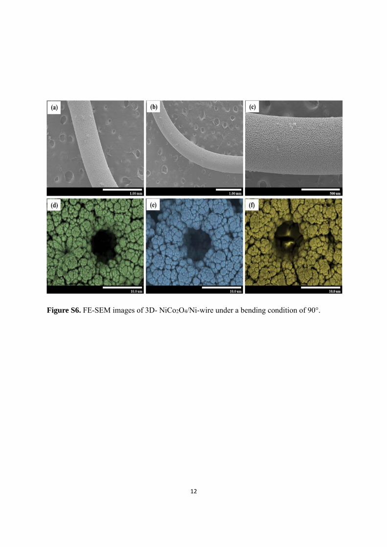
Figure S6. FE-SEM images of 3D- NiCo2O4/Ni-wire under a bending condition of 90°.
13
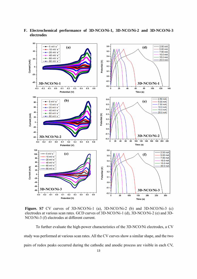
F. Electrochemical performance of 3D-NCO/Ni-1, 3D-NCO/Ni-2 and 3D-NCO/Ni-3 electrodes
Figure. S7 CV curves of 3D-NCO/Ni-1 (a), 3D-NCO/Ni-2 (b) and 3D-NCO/Ni-3 (c) electrodes at various scan rates. GCD curves of 3D-NCO/Ni-1 (d), 3D-NCO/Ni-2 (e) and 3D-NCO/Ni-3 (f) electrodes at different current.
To further evaluate the high-power characteristics of the 3D-NCO/Ni electrodes, a CV
study was performed at various scan rates. All the CV curves show a similar shape, and the two
pairs of redox peaks occurred during the cathodic and anodic process are visible in each CV,

14
indicating the pseudocapacitive properties of the electrode (Faradaic reaction: Ni and Co). The
shape of the CV curves was not significantly changed but the peak current increased with
increasing scan rate, indicating that the 3D-NCO/Ni electrodes are beneficial to fast faradaic
reaction and high rate response at higher scan rates. Additionally, with the sweep rate increasing
from 5 to 80 mV s-1, the position of the anodic and cathodic peaks slightly shifted towards
positive and negative potentials, respectively. This phenomenon may be due to the high
electron hopping resistance (internal resistance of the electrode) or the mass-transport
limitation of ions from the electrolyte to the electrode surface in order to satisfy the electronic
neutralization at the electrode during the faradaic reaction 11. But the potential shift of the
anodic (ca. 70 mV) and cathodic (ca. 50 mV) peaks were smaller, suggesting that 3D-NiCo2O4
has low polarization, resulting from the high electrical conductivity (low resistance) of the 3D-
Ni backbone and the good contact between the electroactive materials and the 3D-Ni current
collector. This can be further confirmed through electrochemical impedance spectroscopy (EIS)
(Figure S8).

15
G. Calculation and analysis
Three-electrode analysis
The volumetric, gravimetric and areal capacitance of the as-fabricated electrode
materials were calculated from the cyclic voltammetry and galvanostatic charge/discharge
curves using the following Equations 12-16:
Cyclic Voltammetry:
VS
idVC
2 …………….. (1)
Galvanostatic charge/discharge:
)/( dtdv
IC …………….. (2)
v
CC v …………….. (3)
m
CC g …………….. (4)
A
CC a …………….. (5)
Where C is the capacitance (F), Cv is the volumetric capacitance (F cm-3), Cg is the gravimetric
capacitance (F g-1), Ca is the areal capacitance (F cm-2), S is the scan rate (mV s-1), V is the
voltage window (V), I is the discharge current (A), dv/dt is the average slope of the discharge
curve (V s-1), v is the total volume of the electrode material (cm3), m is the mass of the
electroactive material (g), A is the area of the electrode material (cm2), and ∫idV is the integral
area of the CV curve (A).

16
Device analysis
The volumetric (Cv) and gravimetric (Cg) capacitance was calculated from the cyclic
voltammetry and galvanostatic charge/discharge curves using the equation below 12-16:
Cyclic Voltammetry:
VS
idVCD
2
…………….. (6)
Galvanostatic charge/discharge:
)/( dtdv
IC D …………….. (7)
v
CC D
v …………….. (8)
m
CC D
g …………….. (9)
For single electrode capacitance:
)(4 gvs CC …………….. (10)
Where CD is the device capacitance (F), Cs is the single electrode capacitance (F), v is the total
volume of the device (cm3), and m is the total mass of the device (g)
Energy and power density
Volumetric as well as gravimetric energy density (E) and power density (P) of the
device were calculated from the discharge curves as the follows 16-18;
vm
VdtIE …………….. (11)
t
EP …………….. (12)
Where I is the discharge current (A), ∫Vdt is the integral area of the discharge curve (V s), m is
the total mass of the electroactive material in both electrodes (g), v is the total volume of the

17
device (cm3), and t is the discharge time (s).
H. Electrochemical impedance spectroscopy
Figure. S8 (a) Nyquist plots of Ni-wire and 3D-Ni electrodes. (b) Nyquist plots of 3D-NCO/Ni-1, 3D-NCO/Ni-2 and 3D-NCO/Ni-3 electrodes. The inset is the high frequency region of the Nyquist plots.
To further investigate the fundamental behavior of the fabricated electrodes,
electrochemical impedance spectroscopy (EIS) measurements were performed. Figure S8a
and S6b show the Nyquist plots of the Ni-wire, 3D-Ni, 3D-NCO/Ni-1, 3D-NCO/Ni-2 and 3D-
NCO/Ni-3 electrodes. The inset shows the amplified part of the high frequency region. The
Nyquist plots of Ni and 3D-Ni display (Figure S8a) the negligible charge transferred resistance,
which confirms the good electrical conductivity of the current collectors.
The Nyquist plots of the 3D-NCO/Ni-1, 3D-NCO/Ni-2 and 3D-NCO/Ni-3 electrodes
(Figure S8b) are composed of two distinct parts, a semi-circle arc at the high-frequency region
followed by the linear line at the low frequency region. In the high-frequency region, the
intercept at the Z’-axis of the Nyquist plots indicates the ohmic resistance of the electroactive
material, the electrolyte (Rs) and the electroactive material/ current collector interface 19-21. The
ohmic resistance values of the 3D-NCO/Ni-1, 3D-NCO/Ni-2 and 3D-NCO/Ni-3 electrodes

18
were found to be 0.31, 0.30 and 0.31 Ω, respectively. The semicircle arc in the mid-frequency
region indicates the charge transfer resistance at the electrode/electrolyte interface. The charge
transfer resistances of the 3D-NCO/Ni-1, 3D-NCO/Ni-2 and 3D-NCO/Ni-3 electrodes are
relatively small.
The lower ohmic and charge transfer resistance values of the as-fabricated electrodes
confirmed their good electrical conductivity, which allows fast electron transfer between the
current collector and the electroactive sites to assist the Faradaic reactions. The inclined portion
of the curve (about 45°) in the low frequency region is attributed to the frequency dependence
of ion diffusion at the electrolyte/electrode interface (Warburg impedance)19-21. In addition, the
nearly vertical line in the low frequency region indicates the higher capacitive behavior of the
electrodes.

19
I. Gravimetric and areal capacitance
Figure. S9 Gravimetric (a) and areal (b) capacitances of the 3D-NCO/Ni-1, 3D-NCO/Ni-2and 3D-NCO/Ni-3 electrodes as a function of scan rates. Gravimetric (c) and areal (d) capacitance as a function of current.

20
J. Volumetric and gravimetric capacitance of fiber supercapacitor
Figure. S10 (a) Volumetric and gravimetric capacitances of solid state symmetric device as a function of scan rate. (b) Volumetric and gravimetric capacitances at different current.
21
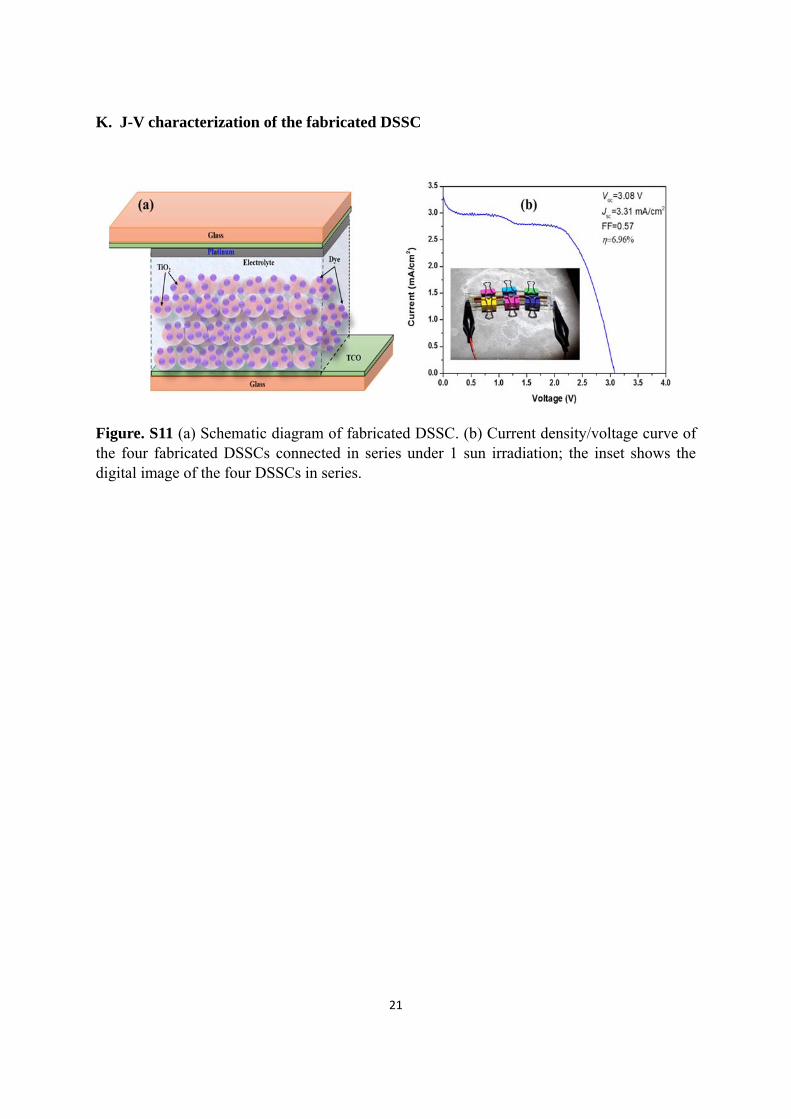
K. J-V characterization of the fabricated DSSC
Figure. S11 (a) Schematic diagram of fabricated DSSC. (b) Current density/voltage curve of the four fabricated DSSCs connected in series under 1 sun irradiation; the inset shows the digital image of the four DSSCs in series.
22
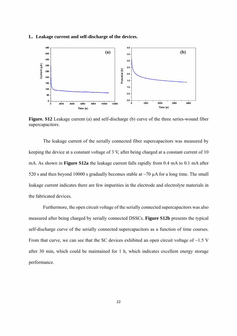
L. Leakage current and self-discharge of the devices.
Figure. S12 Leakage current (a) and self-discharge (b) curve of the three series-wound fiber supercapacitors.
The leakage current of the serially connected fiber supercapacitors was measured by
keeping the device at a constant voltage of 3 V, after being charged at a constant current of 10
mA. As shown in Figure S12a the leakage current falls rapidly from 0.4 mA to 0.1 mA after
520 s and then beyond 10000 s gradually becomes stable at ~70 µA for a long time. The small
leakage current indicates there are few impurities in the electrode and electrolyte materials in
the fabricated devices.
Furthermore, the open circuit voltage of the serially connected supercapacitors was also
measured after being charged by serially connected DSSCs. Figure S12b presents the typical
self-discharge curve of the serially connected supercapacitors as a function of time courses.
From that curve, we can see that the SC devices exhibited an open circuit voltage of ~1.5 V
after 30 min, which could be maintained for 1 h, which indicates excellent energy storage
performance.

23
References:
1. X. H. Xia, J. P. Tu, Y. Q. Zhang, Y. J. Mai, X. L. Wang, C. D. Gu and X. B. Zhao, The
Journal of Physical Chemistry C, 2011, 115, 22662-22668.
2. H. Jiang, Y. Guo, T. Wang, P.-L. Zhu, S. Yu, Y. Yu, X.-Z. Fu, R. Sun and C.-P. Wong,
RSC Advances, 2015, 5, 12931-12936.
3. Z.-Q. Liu, K. Xiao, Q.-Z. Xu, N. Li, Y.-Z. Su, H.-J. Wang and S. Chen, RSC Advances,
2013, 3, 4372-4380.
4. W. Li, L. Xin, X. Xu, Q. Liu, M. Zhang, S. Ding, M. Zhao and X. Lou, Scientific Reports,
2015, 5, 9277.
5. Y. Wang, K. Cheng, D. Cao, F. Yang, P. Yan, W. Zhang and G. Wang, Fuel Cells, 2015,
15, 298-305.
6. B. Cui, H. Lin, Y.-z. Liu, J.-b. Li, P. Sun, X.-c. Zhao and C.-j. Liu, The Journal of
Physical Chemistry C, 2009, 113, 14083-14087.
7. V. H. Nguyen and J.-J. Shim, Journal of Power Sources, 2015, 273, 110-117.
8. J. G. Kim, D. L. Pugmire, D. Battaglia and M. A. Langell, Applied Surface Science,
2000, 165, 70-84.
9. J. F. Marco, J. R. Gancedo, M. Gracia, J. L. Gautier, E. Ríos and F. J. Berry, Journal of
Solid State Chemistry, 2000, 153, 74-81.
10. V. M. Jiménez, A. Fernández, J. P. Espinós and A. R. González-Elipe, Journal of
Electron Spectroscopy and Related Phenomena, 1995, 71, 61-71.
11. J. W. Lee, T. Ahn, D. Soundararajan, J. M. Ko and J.-D. Kim, Chemical
Communications, 2011, 47, 6305-6307.
12. Y. Song, X. Cai, X. Xu and X.-X. Liu, Journal of Materials Chemistry A, 2015, 3,
14712-14720.
24
13. A. Ramadoss, B. Saravanakumar, S. W. Lee, Y.-S. Kim, S. J. Kim and Z. L. Wang, ACS
Nano, 2015, 9, 4337-4345.
14. A. Ramadoss, B. Saravanakumar and S. J. Kim, Nano Energy, 2015, 15, 587-597.
15. H. Jin, L. Zhou, C. L. Mak, H. Huang, W. M. Tang and H. L. Wa Chan, Journal of
Materials Chemistry A, 2015, 3, 15633-15641.
16. S. T. Senthilkumar, R. K. Selvan, Y. S. Lee and J. S. Melo, Journal of Materials
Chemistry A, 2013, 1, 1086-1095.
17. B. Akinwolemiwa, C. Peng and G. Z. Chen, Journal of The Electrochemical Society,
2015, 162, A5054-A5059.
18. J. Y. Kim and I. J. Chung, Journal of The Electrochemical Society, 2002, 149, A1376-
A1380.
19. J. Yan, Z. Fan, T. Wei, W. Qian, M. Zhang and F. Wei, Carbon, 2010, 48, 3825-3833.
20. W. Zhang, H. Lin, Z. Lin, J. Yin, H. Lu, D. Liu and M. Zhao, ChemSusChem, 2015, 8,
2114-2122.
21. M. Liu, W. W. Tjiu, J. Pan, C. Zhang, W. Gao and T. Liu, Nanoscale, 2014, 6, 4233-
4242.