Flexible electronics under strain: a review of mechanical ...chung3/papers/2016_JMS.pdf ·...
35
REVIEW Flexible electronics under strain: a review of mechanical characterization and durability enhancement strategies K. D. Harris 1,2 • A. L. Elias 1,3 • H.-J. Chung 3 Received: 14 September 2015 / Accepted: 6 December 2015 / Published online: 21 December 2015 Ó Her Majesty The Queen in Right of Canada 2015 Abstract Flexible electronics incorporate all the func- tional attributes of conventional rigid electronics in formats that have been altered to survive mechanical deformations. Understanding the evolution of device performance during bending, stretching, or other mechanical cycling is, there- fore, fundamental to research efforts in this area. Here, we review the various classes of flexible electronic devices (including power sources, sensors, circuits and individual components) and describe the basic principles of device mechanics. We then review techniques to characterize the deformation tolerance and durability of these flexible devices, and we catalogue and geometric designs that are intended to optimize electronic systems for maximum flexibility. Introduction The development of flexible electronics has received con- siderable attention recently, as R&D efforts in this area are ultimately expected to facilitate extremely valuable device applications. Researchers are now frequently describing devices or techniques that pave the way toward con- formable sensors for health-care applications, electronic skin for versatile and adaptable robots, or flexible analogues of conventional consumer electronics such as e-readers, mobile phones, or televisions. Some recently published images representing a diverse range of these flexible devices are collected in Fig. 1. Because the range of applications is extremely broad, device flexibility requirements are quite varied. In some cases, extremely high strain implementations are antici- pated, including sensing/communications devices inte- grated directly onto skin or other organs (e.g. the devices in Fig. 1b, d) or electronics embedded into clothing or other textiles. In other applications, small but repetitive strain cycles are expected, while a different range of applications require tolerance of moderate one-time strains. Even if the electronics are intended to be used while firmly fixed in place, they must still be able to withstand various stresses and strains inherent to their manufacturing process or deployed location, such as bending deformation in a roll- to-roll manufacturing line, thermal expansions from vari- ations in ambient temperature, or abrasion as a result of weathering or user handling. This evidence all points toward a need for high-quality R&D directed specifically toward improving the strain tolerance of electronic mate- rials and devices. Flexible devices must be capable of undergoing defor- mation and at the same time the functional properties and electronic performance parameters must be unaffected by the strain process. The electrical resistance of a flexible electrode, for example, should be low before, during and after a deformation cycle, while the power conversion efficiency of a flexible solar cell should be large throughout an entire strain process. Similarly, for devices that actively measure strains or harvest energy from strain (strain sen- sors and piezoelectric generators, for instance), the response to strain should be consistent throughout the entire device lifetime. & K. D. Harris [email protected] 1 National Institute for Nanotechnology, Edmonton, AB, Canada 2 Department of Mechanical Engineering, University of Alberta, Edmonton, AB, Canada 3 Department of Chemical & Materials Engineering, University of Alberta, Edmonton, AB, Canada 123 J Mater Sci (2016) 51:2771–2805 DOI 10.1007/s10853-015-9643-3
Transcript of Flexible electronics under strain: a review of mechanical ...chung3/papers/2016_JMS.pdf ·...
REVIEW
Flexible electronics under strain: a review of mechanicalcharacterization and durability enhancement strategies
K. D. Harris1,2 • A. L. Elias1,3 • H.-J. Chung3
Received: 14 September 2015 / Accepted: 6 December 2015 / Published online: 21 December 2015
� Her Majesty The Queen in Right of Canada 2015
Abstract Flexible electronics incorporate all the func-
tional attributes of conventional rigid electronics in formats
that have been altered to survive mechanical deformations.
Understanding the evolution of device performance during
bending, stretching, or other mechanical cycling is, there-
fore, fundamental to research efforts in this area. Here, we
review the various classes of flexible electronic devices
(including power sources, sensors, circuits and individual
components) and describe the basic principles of device
mechanics. We then review techniques to characterize the
deformation tolerance and durability of these flexible
devices, and we catalogue and geometric designs that are
intended to optimize electronic systems for maximum
flexibility.
Introduction
The development of flexible electronics has received con-
siderable attention recently, as R&D efforts in this area are
ultimately expected to facilitate extremely valuable device
applications. Researchers are now frequently describing
devices or techniques that pave the way toward con-
formable sensors for health-care applications, electronic
skin for versatile and adaptable robots, or flexible
analogues of conventional consumer electronics such as
e-readers, mobile phones, or televisions. Some recently
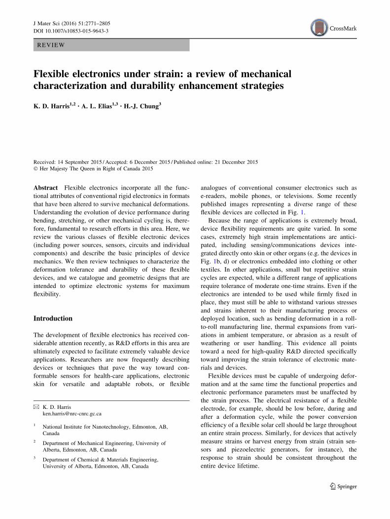
published images representing a diverse range of these
flexible devices are collected in Fig. 1.
Because the range of applications is extremely broad,
device flexibility requirements are quite varied. In some
cases, extremely high strain implementations are antici-
pated, including sensing/communications devices inte-
grated directly onto skin or other organs (e.g. the devices in
Fig. 1b, d) or electronics embedded into clothing or other
textiles. In other applications, small but repetitive strain
cycles are expected, while a different range of applications
require tolerance of moderate one-time strains. Even if the
electronics are intended to be used while firmly fixed in
place, they must still be able to withstand various stresses
and strains inherent to their manufacturing process or
deployed location, such as bending deformation in a roll-
to-roll manufacturing line, thermal expansions from vari-
ations in ambient temperature, or abrasion as a result of
weathering or user handling. This evidence all points
toward a need for high-quality R&D directed specifically
toward improving the strain tolerance of electronic mate-
rials and devices.
Flexible devices must be capable of undergoing defor-
mation and at the same time the functional properties and
electronic performance parameters must be unaffected by
the strain process. The electrical resistance of a flexible
electrode, for example, should be low before, during and
after a deformation cycle, while the power conversion
efficiency of a flexible solar cell should be large throughout
an entire strain process. Similarly, for devices that actively
measure strains or harvest energy from strain (strain sen-
sors and piezoelectric generators, for instance), the
response to strain should be consistent throughout the
entire device lifetime.
& K. D. Harris
1 National Institute for Nanotechnology, Edmonton, AB,
Canada
2 Department of Mechanical Engineering, University of
Alberta, Edmonton, AB, Canada
3 Department of Chemical & Materials Engineering,
University of Alberta, Edmonton, AB, Canada
123
J Mater Sci (2016) 51:2771–2805
DOI 10.1007/s10853-015-9643-3
It should also be noted that the term flexible can refer to
tolerance of a range of different mechanical deformation
modes. At the dawn of the research field, ‘‘flexible elec-
tronics’’ usually indicated bendable versions of planar
electronics. More recently, foldable, stretchable and
twistable modes have also been enabled through advanced
device designs, with the current state-of-the-art represented
by three-dimensional, non-planar geometries. All of these
deformation modes are relevant to the present review, and
we will use the term ‘‘flexible electronics’’ to broadly
represent devices that accommodate any of these
mechanical deformation modes. To evaluate flexibility or
strain tolerance, researchers rely on a wide range of tech-
niques such as cyclic testing in bending or stretching
modes, scratch testing, or peel testing. Each of these
characterization techniques reveals different information
about the mechanical reliability of the materials and
devices. It is the intention of this paper to review these test
procedures and catalogue the progress researchers have
made to maximize the durability of materials and devices
as measured by each of these mechanical characterization
techniques.
The review is organized as follows: we begin by sur-
veying materials, devices and fabrication techniques to
introduce the subject matter. Because considerable review
material already exists in these areas, we provide only an
overview and, wherever possible, direct the reader toward
additional information. We then outline basic concepts in
mechanics that pertain to flexible or stretchable devices.
We write to target the non-expert and provide the basis for
understanding of the topics in subsequent sections. Fol-
lowing this, we review in detail the types of mechanical
tests that are performed to evaluate the strain tolerance of
materials and devices. We discuss the equipment required
to perform each characterization process, and we overview
measured results for a variety of flexible electronic devices
(as organized by the mechanical characterization technique
rather than by device type). Because mechanical mea-
surements go hand-in-hand with efforts to improve device
longevity, we also discuss ongoing research activities that
are specifically directed toward improving the durability of
flexible electronic devices.
Materials, applications and fabrication techniques
Conductors, semiconductors and insulators
The basic building blocks for electronic components are
electrical conductors, semiconductors and insulators, and
many research efforts have been made to identify flexible
or stretchable materials in each of these categories [5].
Fig. 1 Examples of flexible electronic devices, including a an array
of flexible pressure sensors (reproduced with permission) [1], b a
piezoelectric energy harvester integrated with a bovine diaphragm
(reproduced with permission) [2], c a twistable LED array
(reproduced with permission) [3] and d a stretchable and skin-
mountable physiological measurement device (reproduced with
permission) [4]
2772 J Mater Sci (2016) 51:2771–2805
123
Metals are the best known electrical conductors. In high-
performance electronics applications, the conductivity of
metallic films (r * 104 - 106 S/cm) is highly advanta-
geous (possibly even essential), and these materials are
often capable of withstanding modest bending-mode
deformations [6]. Metallic films can be applied and pat-
terned either in a conventional process involving vapour
deposition followed by photolithography [6], or by printing
a nanoparticle-loaded ink and sintering to form an elec-
trically continuous film [7, 8]. The key challenge in the
latter case has been developing sintering conditions that are
compatible with plastic substrates.
In applications demanding stretching or large-scale
bending, however, metal films are often found to be
mechanically inadequate [9–13], and this has led to the
development of several alternative geometries and mate-
rials [14]. For instance, gallium/indium mixed in propor-
tions near the eutectic point (known as eGaIn) is a metallic
conductor that is also a liquid at room temperature [15].
Electrical conductors incorporating eGaIn or other liquid
metals are capable of tolerating large deformations without
suffering a noticeable loss of electrical conductivity [15–
19], but on the other hand complex fabrication strategies
are often required, and strain-tolerant encapsulation to
prevent leakage is certain to be an issue.
Percolated networks of conducting nanowires (NWs) are
also used to form strain-tolerant films for electronics
applications. With this design strategy, large quantities of
high-aspect ratio conductors are cast onto a substrate to
form a continuous network that is either randomly arranged
or guided with an aligning field [6, 20–22]. Junctions
between NWs increase the electrical resistance of the
network, but because free volume exists around the elec-
trically conducting network, NW meshes are able to
accommodate mechanical strain by hinging/sliding at
points where individual NWs intersect one another [23].
These percolated networks also have the added advantage
of redundant pathways for charge transport. If links are
damaged within the conducting network, charge is redi-
rected to neighbouring links without isolating large sec-
tions of the device. Electrically conducting films of this
nature have been formed in a variety of materials including
carbon nanotubes (CNTs) [6, 24, 25], silver nanowires [9,
26, 27] and copper nanowires [9, 28]. A comprehensive
review of this topic is given in a recent publication by Yao
and Zhu [29].
Polymeric materials that naturally have some degree of
mechanical compliance can also be employed to form
strain-tolerant electrical connections. Several strategies are
available to ensure both electrical conductivity and
mechanical durability coexist in the same material. These
include loading a mechanically compliant, non-conducting
elastomer with electrically conducting fillers such as metals
or carbon [10, 11, 30–32], or choosing, and appropriately
doping, a p-conjugated polymer [9, 33–35]. The first
approach has a long history, with the concept of ‘‘con-
ductive rubbers’’ dating back to the 1950s [32]. The
modulus of these composites can be predicted using
models such as the Halpin–Tsai model [36, 37], taking into
account the mechanical properties of both the matrix and
filler materials, the volume fractions, the filler dispersion,
the shape of filler particles and the alignment of filler
within the matrix. With sufficient loading (i.e. above the
percolation threshold), the fillers (most commonly car-
bonaceous particles) tend to dictate the electrical properties
of the composite. Numerous applications of these con-
ducting composites have been identified including dissi-
pation of static charge and electromagnetic interference
shielding; however, the conductivity of carbon-filled rub-
bers has historically been too low (\0.1 S/cm) for most
electronics applications [10]. With the development of
nanofillers such as carbon nanotubes or other NWs, how-
ever, reduced loading is often required to achieve perco-
lation, and conductivities in excess of 100 S/cm are now
being measured [10].
Conjugated polymers such as polypyrrole, polyaniline or
polythiophenes are also used in flexible electronics appli-
cations [9, 11, 33–35, 38–40], and in many cases com-
posites (conducting polymers loaded with nanotubes, for
instance) are also formed to further tailor mechanical or
electrical properties [11]. Presently, the key organic
material is the polythiophene derivative poly(3,4-
ethylenedioxythiophene):poly(styrenesulfonate), or PED-
OT:PSS [41]. This material is typically cast from an
aqueous suspension, and additives including small polar
molecules or surfactants have been included to improve
conductivity [9]. The best conductivities attained with
these materials are greater than 1000 S/cm, and processing
is performed from solution, which is an advantage when
high-volume manufacturing in considered. On the other
hand, it is important to be aware that the use of polymeric
materials does not necessarily ensure favourable mechan-
ical properties, and moreover conducting polymers do tend
to have considerably lower electrical conductivity and
stability than metallic conductors [25].
Graphene has also been utilized as an electrical con-
ductor in applications requiring mechanical deformations
[24, 42]. The material is intrinsically strong and flexible
[43], and it has fairly low resistance in an undoped state
(*6 kX/h for an undoped monolayer). The conductivity
can, moreover, be further improved through electrostatic or
chemical doping to increase the charge carrier concentra-
tion. The highest performance graphene tends to be pro-
duced by mechanical exfoliation of bulk graphite or in
chemical vapour deposition reactions. The former, how-
ever, is not considered to be easily scalable to high-volume
J Mater Sci (2016) 51:2771–2805 2773
123
manufacturing, while the latter is not directly compatible
with plastic substrates and requires a transfer step [44]. An
alternative, high-volume technique that may be advanta-
geous for flexible electronics applications is chemical
synthesis and printing directly from solution [45].
Transparent conductors make up an important subset
within the materials for flexible electrical conductors [9,
25, 46–49]. All of the mechanical and electrical require-
ments for flexible conductors must still be satisfied, while
provisions for light transmission must also be engineered
into the material [25]. The spectral range for transparency
is determined by the intended application: for example,
displays require good transparency across the wavelengths
visible to the human eye (400–700 nm), whereas solar cells
require broader transparency as weighted by the power of
the solar spectrum and the absorbance of the photoactive
layer. Thin metal films, conductive rubbers and most p-conjugated polymer systems tend not to meet the necessary
performance standards for transparent conductors, while
graphene, several percolated NW systems and PEDOT:PSS
appear to be well suited. At present, the materials most
commonly used in these applications are the transparent
conducting oxides (TCOs) such as indium tin oxide (ITO)
[47, 48]. These materials are well known to be quite brittle,
but in applications requiring only moderate flexibility, the
device geometry can be designed to allow TCOs to be
included.
Many of the strategies used to fabricate flexible or
stretchable conductors can also be adapted to form flexible
semiconductors [9, 11, 20, 21, 46]. Both semiconducting
NWs [22, 46, 50] and semiconducting organics (polymers
and small molecules) [11, 35, 38, 39, 51, 52] have been
synthesized and cast from solution for flexible electronics
applications. The carbon nanomaterials (graphene and
CNTs) have also been used successfully, although in this
case it is often necessary to include a dedicated processing
step to ensure semiconducting behaviour (e.g. removing
metallic CNT links) [6, 24, 42, 53]. Despite this range of
materials, the formation of deformation-tolerant semicon-
ductors with good electronic properties does tend to rep-
resent a considerably more difficult problem than the
formation of strain-tolerant conductors. Even organic
semiconductors often degrade markedly under strain [54,
55], and some results reveal correlations between charge
carrier mobility and elastic modulus [56], or solar cell
performance and elastic modulus [57]. This behaviour is
thought to be mediated by molecular order and crys-
tallinity, which generally facilitate good charge carrier
mobility while simultaneously stiffening the materials.
This implies that flexibility and favourable electronic
properties are inversely related for organic semiconductors
[58, 59]. It is also notable that conventional semiconductor
materials, such as silicon or III–V materials, have been
revisited as key components for flexible electronics. Their
utilization is usually accompanied with advanced designs
that will be discussed later in the review. Also, in the case
of flexible solar cells, perovskites are particularly important
light-absorbing semiconductors [60, 61].
Flexible insulators tend to be discussed less often in the
literature than conducting or semiconducting counterparts,
but they are no less critical to the successful operation of
several electronic devices. Because field-effect transistors
(FETs) demand the most specific functional properties,
flexible insulators are usually reviewed in the context of
these FET applications [6, 24, 51]. From this standpoint, an
ideal insulator is mechanically compliant, can be deposited
at low temperature without vacuum techniques, has a large
dielectric constant (j) and forms a continuous, pinhole-free
dielectric at low thickness. The ceramic oxides such as
SiO2 and the ‘‘high-j’’ dielectrics, ZrO2, TiO2, HfO2 and
Al2O3, developed for conventional rigid electronics gen-
erally achieve the best electronic performance, but they
also tend to be brittle. In applications requiring only
modest flexibility, devices incorporating these oxides can
achieve acceptable flexibility with careful design of the
geometry, but if large, repeated deformations or stretcha-
bility is necessary, then polymeric dielectrics are generally
employed. Many polymeric materials can be deposited
from solution by spin-coating or printing, and inexpensive
materials such as polydimethylsiloxane (PDMS), poly-
methylmethacrylate (PMMA) or polyimide (PI) have been
successfully used in FET applications. Another material,
parylene-C, can be deposited from the vapour phase,
forming highly conformal coatings. Because polymers with
various chemical compositions are available, the designer
can exercise considerable freedom in choosing organic
insulators with the best possible compatibility (i.e. solu-
bility, wettability, thermal behaviour, etc.) with other
materials in the device stack. Hybrid gate insulators that
include both high-j oxides and polymers have also been
demonstrated on plastic substrates, and the associated FET
devices had excellent electronic properties coupled with
flexibility [62].
Not to be neglected, barrier layers are often included in
flexible electronics systems to prevent diffusion of gases
into the device and the associated degradation of the
electronic materials [63]. Often encapsulating the elec-
tronics system, these materials can be subjected to high
strain and/or abrasion and must be carefully chosen to
withstand their mechanical environment.
Substrates
Substrates are also a critically important consideration as
their mechanical properties can dominate those of the
integrated system. The materials can generally be grouped
2774 J Mater Sci (2016) 51:2771–2805
123
into three broad categories: plastic films, metal foils and
fibrous materials (including paper and textiles).
Plastic films are the most common flexible substrates
noted in the literature [9, 11, 64–70]. Properties vary
considerably from material to material, but in general
plastic films tend to be relatively inexpensive and light-
weight, making them well suited to high-volume manu-
facturing. Some key materials include polyethylene
terephthalate (PET), polyethylene naphthalate (PEN),
polycarbonate (PC), polyethersulfone (PES), polyimide
(PI) and polyarylate (PAR); many other options are also
available as necessary. Because the material properties
vary greatly, it is important to consider thermal stability,
mechanical stability, solvent resistance, surface energy/
wettability, diffusivity, optical clarity, surface smoothness
and cost to effectively guide the selection of substrates for
any given application [70]. A good discussion of process-
ing temperatures can be found in the review by Fortunato
et al. [65]. This publication also discusses the important
issue of device deformation induced by mismatching
coefficients of thermal expansion for plastic substrates and
typical device materials.
In applications where stretchability is important, most of
the materials noted above are abandoned in favour of
highly compliant elastomers such as polydimethylsiloxane
(PDMS), polyurethanes, or the multiblock copolymer
styrene ethylene butadiene styrene (SEBS) [9, 11, 71].
Cotton et al. demonstrated that the mechanical properties
of PDMS could be photopatterned to locally soften the
substrate in regions intended to support interconnects
rather than rigid components [72]. In another interesting
approach, stretchable devices were also formed on non-
elastomeric substrates by cutting a strain-relieving pattern
into the substrate [73]. With these perforated substrates,
hole shape dynamically varies to accommodate tensile
strain.
Metal foils are commonly introduced when high-tem-
perature processing is a requirement [64, 66, 68]. As sub-
strates, metals tend to be relatively temperature resistant,
and they are also excellent electrical and thermal conduc-
tors, good barriers against the diffusion of water and oxy-
gen, and relatively resistant to most solvents. Stainless steel
represents the leading material, but other options (such as
titanium or copper foils) are also available if particular
attributes of these metals are advantageous. The weight of
metal foils is a key disadvantage, and the materials also
tend to be more expensive and less flexible than plastic
substrates.
Due to its extremely low cost, many researchers also
endeavour to use paper as a substrate for electronic com-
ponents and circuits [33, 74, 75]. Paper is inexpensive
(*10 ¢/m2), even when compared against commodity
plastics such as PET (*2 $/m2). Bulk paper does,
however, have a range of drawbacks when electronics
applications are considered: water and other solvents can
be absorbed by the material and may affect the electronic
components, the surface is generally rough making device
fabrication challenging, and light scatters from surface
irregularities which may rule out some applications. Most
of these issues can be addressed with chemical treatments,
but these treatments do add cost to the manufacturing
process. Nevertheless, the potential for extremely low-cost
manufacturing means that paper cannot be discounted as a
substrate material.
Many of the challenges associated with paper substrates
also extend to devices intended to be integrated with
clothing or other textiles [75–80]. Economically, these
substrates are important as the market for clothing with
integrated electronics is ultimately expected to be large.
Researchers are, however, facing numerous challenges. For
example, textiles are composed of numerous individual
fibres, making fabrication of surface-mounted devices
difficult, and most textiles are also capable of transmitting
air and absorbing large amounts of water which can affect
electronic components both chemically and mechanically.
Typical human interactions with clothing are also impor-
tant: the clothing must be washable, and the integrated
electronics should be sufficiently compliant that they not
only survive mechanical deformation, but feel comfort-
able to the wearer (imagine sitting on a fold). One useful
advantage of textiles with respect to the integration of
electronics, however, is that fibres themselves can be ren-
dered electrically conducting by blending in conducting
components [75, 78, 81].
Applications: discrete devices and integrated
systems
Using the set of basic materials described above, a wide
array of passive and active flexible electronic components
may be fabricated, and these discrete devices can be
arranged to form power supplies, sensing platforms or
complete electronic systems. Flexible thin-film transistors
(TFTs) are key components in many of these systems, and
generally field-effect transistors that are utilized in con-
temporary applications [6, 21, 24, 46, 65, 66, 82–85]. In the
most common implementation, FETs are three-terminal
devices that operate based on modulation of the electrical
conductivity in a patterned semiconductor ‘‘channel’’.
Electrical current is injected into and extracted from the
channel at high-conductivity electrodes denoted the
‘‘source’’ and ‘‘drain’’, while the conductivity of the
channel is determined by the voltage at a ‘‘gate’’ electrode.
The gate is separated from the source, drain and channel by
a ‘‘gate insulator’’, but it is capacitively coupled to the
channel such that the concentration of charge carriers in the
J Mater Sci (2016) 51:2771–2805 2775
123
channel is directly tied to the gate voltage. Varying this
voltage, therefore, adjusts the current flowing between
source and drain. These devices act as switches or ampli-
fiers in electrical circuitry, and stimulus-responsive gates
can also form the basis of sensing devices. Some of the key
parameters that describe FET performance are the charge
carrier mobility (l), ratio of currents in the on/off states
(Ion/Ioff), threshold voltage (Vth) and the ‘‘subthreshold
slope’’ which describes how readily the device switches
between on/off states in response to small variations in gate
voltage. In a deformation-tolerant TFT, the high-conduc-
tivity electrodes, the semiconducting channel and the gate
insulator must all be capable of withstanding mechanical
deformation. Generally, flexible FETs based on inorganic
semiconductors, including silicon, have the best measured
electronic performance parameters, although steps must be
taken to ensure that deformation tolerance is accept-
able and fabrication temperatures are compatible with
flexible substrates [46, 65, 82, 86, 87]. Devices based on
both organic materials [51] and carbon nanomaterials
(CNTs and graphene) [6, 24] have also been fabricated, but
in the former oxidation-induced degradation is problematic
and performance metrics tend to be lower than for inor-
ganic materials, while in the latter achieving appropriate
electronic properties (i.e. separating semiconducting from
metallic CNTs, or engineering graphene with an appro-
priate bandgap) can be challenging.
Memory elements are also critical components of many
electronic devices, as they are used to store data and pro-
gramming information. High-value consumer products
such as televisions, mobile phones and e-readers incorpo-
rate memory, and therefore flexible versions of these
products will ultimately require flexible memory devices to
be developed. Many types of memory elements are avail-
able, and it is beyond the scope of this review to describe
the operating principles for the various classes. This
information was thoroughly reviewed by Han et al. [88],
and the authors also provide considerable information on
progress toward developing flexible memory elements.
Some of the key issues include developing low-tempera-
ture processing conditions that are compatible with flexible
substrates, adding appropriate planarization layers to
reduce the influence of substrate roughness, and ensuring
that process solvents do not damage the substrate or other
layers of the device stack.
Integrating lighting with electronic circuitry allows
active displays to be formed, and many research advances
leading toward the creation of flexible displays have also
appeared in the literature. Light-emitting diodes (LEDs)
are the components most commonly suggested as lighting
elements for flexible displays (and also for other applica-
tions such as automotive lighting and biomedical imaging).
In effective devices, LEDs should retain a fixed emission
wavelength under strain, and efficiency (W/W) should
remain high through repeated deformation cycles. Research
efforts to fabricate these flexible LEDs have been ongoing
for several years, such that several reviews on flexible
electronics have incorporated sections devoted to lighting
[6, 10, 21, 39, 89, 90].
Another focus area for flexible electronics is fabrication
of devices for energy generation and storage, including
solar cells, energy scavengers, batteries and supercapaci-
tors. Solar cells (or photovoltaic devices) generate electri-
cal current in response to light absorption at a photoactive
semiconductor [9, 39, 66, 68, 91–95]. Provided that the
photon energy exceeds the semiconductor bandgap, light
striking the semiconductor excites electrons from their
ground states, generating both negative and positive charge
carriers (i.e. electrons and holes). To make up an electrical
current, these carriers are shunted to opposite faces of the
solar cell and extracted through electrodes, one of which
must be transparent in order to admit light into the cell.
Conventional photovoltaics (e.g. silicon) include a p–
n junction to efficiently separate charge carriers [96],
whereas organic photovoltaics use a chemical potential for
this purpose [93]. The key performance parameter is the
power conversion efficiency (PCE), and subsidiary metrics
include the short circuit current density (JSC), open circuit
voltage (VOC), fill factor (FF), series resistance (RS) and
shunt resistance (RSh). A flexible solar cell must retain high
PCE throughout repeated deformation cycles, and incor-
porate robust electrodes, semiconductors, interfacial mod-
ifiers and wiring. A subclass of solar cells, the dye-
sensitized solar cells (DSSCs), also tends to include liquid
electrolytes for charge transfer, and these must also be
effectively contained during strain cycling [68, 92].
Batteries and supercapacitors are both energy storage
devices [33, 34, 75, 95, 97–100]. In a battery, energy is
stored electrochemically, and charge carriers are released
through distinct chemical reactions. Lithium-ion batteries
[98, 99, 101] currently dominate the market with the vast
majority of portable electronics now powered with this
battery type. Li-ion batteries incorporate a lithium com-
pound as a cathode and carbon as an anode and often high-
surface area ‘‘charge collectors’’ are also included at the
electrodes. Electrical current is composed of Li? ions
moving between these electrodes through an electrolyte
medium and charge separator membrane. In direct contrast
with batteries, supercapacitors store energy electrostati-
cally and chemical reactions are not involved in charge
cycling. This is advantageous in that charging/discharging
is fast, and degradation with charge cycling is generally not
severe. Key performance parameters for each of these
devices are energy density (in Wh/g), power density (in
W/g), capacity (in Ah/g, which is a function of discharge
rate) and cycle life (which is the number of charge/
2776 J Mater Sci (2016) 51:2771–2805
123
discharge cycles that can be sustained before the capacity
falls below some critical value, usually 80 %). Batteries
tend to have lower production cost and considerably better
energy density than supercapacitors, while supercapacitors
have superior power density and cycle life. Some of the
key issues faced in developing flexible batteries and
supercapacitors include reliably encapsulating liquid elec-
trolyte or developing high-performance solid-state elec-
trolytes, identifying deformation-tolerant electrode
materials/architectures, and integrating these constituent
materials into a reliable high-performance device [75, 97–
99, 102].
Energy scavenging from mechanical vibrations has also
been suggested as a potential power source for flexible
electronics. In energy scavenging devices, piezoelectric
structures transduce mechanical strain into electrical
charge, and many efforts have been undertaken to identify
promising materials and architectures that maximize power
output [103, 104]. Critical performance parameters include
the piezoelectric charge constants, dij (units: m/V), which
describe the voltage generated along axis i in response to
strain along axis j. One of the key technical issues is that
the mechanical strains required to generate useful power
output often exceed the fracture limits of the brittle
piezoelectric structures.
Another useful class of devices that is expected to be
integrated on deformable substrates are sensing elements,
including chemical sensors, temperature sensors and pres-
sure/strain sensors. Chemical sensors are already wide-
spread, but fabricating analogues on compliant substrates
may lead to implantable devices with improved biocom-
patibility or wearable monitoring systems. Because the
range of possible analytes is enormous, the operating
principles for this class of devices are also quite diverse
[11, 103, 105]. The most common mechanism is chemi-
cally modulated resistance measurement in a semicon-
ducting material, and the associated challenge is the
fabrication of high-quality semiconductors on temperature-
sensitive plastic substrates. To address these issues, nano-
materials or organic semiconductors are often used as
sensing elements, and transfer steps can be included in the
fabrication process.
Pressure/strain/tactile sensors are, in one important
manner, quite different than the remainder of the devices
discussed in this review. Rather than simply tolerating
deformation, most of these devices actually incorporate
deformations as a part of their operating mechanisms. The
operating principles within this class of devices are also
quite varied, but the technologies have been grouped into
several categories (piezoresistive devices, capacitive devi-
ces, piezoelectric devices and optical devices). An excel-
lent review by Bao et al. [106] and several other reviews
include sections devoted to pressure or strain sensors [11,
91, 103]. Because the devices operate by various mecha-
nisms and incorporate a variety of materials, it is difficult
to broadly define the technological challenges for the entire
class of devices. The applications do, however, all require
devices that are able to endure repeated strain cycling, and
therefore mechanical testing to gauge deformation toler-
ance (e.g. tracking the evolution of sensitivity during strain
cycling) is vital for essentially any pressure/strain sensor or
any other deformable sensing platform.
Advances in flexible electronics have also enabled the
development of a wide range of new bionic devices that
could not be realized using rigid materials [66, 76, 79, 107–
111]. External to the body, flexible electronics have been
engineered to conform to the skin and form the basis of a
variety of flexible physiological detectors [107, 112–121],
such as sensors of hydration, pulse, oxygenation or elec-
trophysiological signals. With parallelization, sheets of
these miniaturized, conformal and addressable sensors
have been integrated to form ‘‘electronic skin’’ that may
allow robotics or prostheses to sense their surroundings
with fine resolution [11, 106, 122–126]. Within the body,
flexible electronic devices are also being investigated as
neural interfaces for mapping brain activity [109, 127],
restoring motor function by stimulating spinal neurons
[109, 128] or restoring vision in the eye [129]. Sophisti-
cated, flexible implants have also been used to map other
phenomena in vivo, such as a flexible, elastomeric heart
sock that includes an integrated electrocardiogram and
sensors for pH, temperature and strain [130].
In these biomedical applications, the electronics are
generally expected to be fabricated ex situ on a substrate
chosen for compatibility with the fabrication processes,
then installed on the target tissue (with or without a per-
manent backing) [108, 130]. Once the electronics are in
place, two key issues for both skin-mounted and implanted
devices are ensuring the stability and biocompatibility of
all materials, particularly if long-term use is intended
[131]. For example, the mechanical mismatch between
conventional (i.e. rigid) electronic materials and soft bio-
logical tissue often leads to irritation during motion (either
macroscopic movements of the body or local micromotion
due to blood pulsation) [132]. The mechanical mismatch is
also theorized to promote glial scarring and contribute to
the foreign body response of biological tissue to implants.
For some devices, such as brain–computer interfaces which
aim to measure or transmit electrical signals, these elec-
trically insulating scars are considerable obstacles to device
functionality [133–135]. Because each type of biological
tissue has different characteristics, design constraints built
around stability and biocompatibility tend to be heavily
application specific, but in general devices based on flex-
ible materials are expected to have considerably improved
biocompatibility.
J Mater Sci (2016) 51:2771–2805 2777
123
Fabrication techniques
Flexible or stretchable electronic devices are fabricated
with a wide array of techniques. Exploratory studies
involving either new materials or new applications for
established materials are usually performed by fabricating
simple devices with modest dimensions and using low-
volume fabrication techniques. For example, electrical
conductors are deposited by physical vapour deposition
(PVD) processes (i.e. evaporation or sputtering) [136], and
they are patterned by shadow-masking or simple optical
lithography [136]; semiconductors are spin-cast from
solution if an appropriate solvent can be identified [38], or
they are deposited in PVD or chemical vapour deposition
(CVD) [136, 137] processes; and insulators are spin-cast
from solution or deposited by PVD. In some instances,
spin-coating is substituted with techniques such as drop-
casting, bar-coating or guided assembly [21], and evapo-
ration/sputtering processes are replaced with casting of
metallic inks, CVD, or atomic layer deposition (ALD)
[138, 139].
These techniques are extremely useful for screening
materials, and the equipment required to perform these
basic processes are staples of most research labs special-
izing in flexible electronics. In the long term, however, the
fabrication process truly capitalizes on the potential for
low-cost fabrication by introducing high-volume manu-
facturing techniques in a continuous roll-to-roll (R2R)
process [38, 140–143]. Evaporation, sputtering and CVD
have long been R2R compatible [144–148], although the
high temperatures generally associated with CVD reactions
make development of processing conditions compatible
with plastic substrates more challenging than in analogous
processes on rigid substrates. Considerable effort has also
being directed toward designing ALD reactions that are
R2R compatible [149]. Another staple of high-volume
manufacturing is the set of printing techniques, which can
be sub-divided into two categories: master-printing and
digital printing [140]. The master-printing techniques
require a pre-patterned printing plate as a master and
include the following: flexography (i.e. relief printing) in
which ink is transferred to the substrate from protruding
features in a relief plate; gravure printing (also known as
intaglio printing) in which ink is transferred to the substrate
from the wells in the relief master; offset printing (also
known as planographic printing) in which ink is transferred
from a fully planar master that selectively collects ink
according to an oleophobic versus oleophilic surface pat-
tern; and screen printing in which ink is pressed through a
patterned screen to make an image on the substrate. Digital
printing techniques do not require a master, as they are
instead based upon relative motion between a substrate and
a printing head or nozzle. Inks are dispensed through the
nozzle, and because this relative motion can easily be
reprogrammed, the digital printing techniques tend to be
highly adaptable. The digital printing techniques include
(among others) inkjet printing [7, 150, 151], direct ink
writing [152, 153] and laser patterning, in which ink is
selectively transferred to a substrate based on local heating
from a laser [154, 155]. Other roll-to-roll compatible
techniques include knife-over-edge coating [141, 142],
slot-die coating [141, 142] and electrospinning [21, 156,
157], in which a viscoelastic jet is drawn from a polymer
blend and cast on the substrate.
As opposed to the conventional semiconductor industry,
the fabrication challenges in flexible electronics are not
primarily in miniaturizing devices, but in adapting to
deformation and instability of the substrate [65, 70, 140,
158, 159]. If devices cannot be fabricated directly on the
target, another manufacturing option that is available is
‘‘transfer printing’’ in which materials or complete devices
are pre-fabricated on a convenient substrate before they are
harvested and transferred to a flexible target as if they were
‘‘inks’’ [6, 20, 44, 83, 107, 160, 161]. This technique,
which resembles pick-and-place methods, is relatively
young, but may ultimately be used to form high-quality
inorganic devices with cost-effective R2R fabrication.
Mechanics and modelling
Basic material properties
To understand the mechanics of devices under deforma-
tion, it is first important to define some basic parameters.
Strain is a unitless quantity describing the physical defor-
mation of a shape, and adjectives are often added to further
specify the nature of strain: for example, tensile strain
describes a shape elongated with respect to reference
dimensions, compressive strain describes a compacted
shape, and shear strain describes a deformation in which
parallel planes within the sample are translated in-plane
with respect to one another. Compressive, tensile and shear
strains are graphically depicted in Fig. 2 along with the
applied forces that produce these deformations.
The typical mathematical representation of tensile or
compressive strain, e, is provided in Eq. (1), where Lo is theoriginal dimension and DL is the change in dimension with
respect to this reference state. In tension, a shape that
doubles in length has reached e = 1, while in compression
a shape that is half its original length has reached e = 0.5.
By necessity, shear strain, c, is defined differently and as
shown in Eq. (2), the tangent of the strain angle is used for
this purpose.
2778 J Mater Sci (2016) 51:2771–2805
123
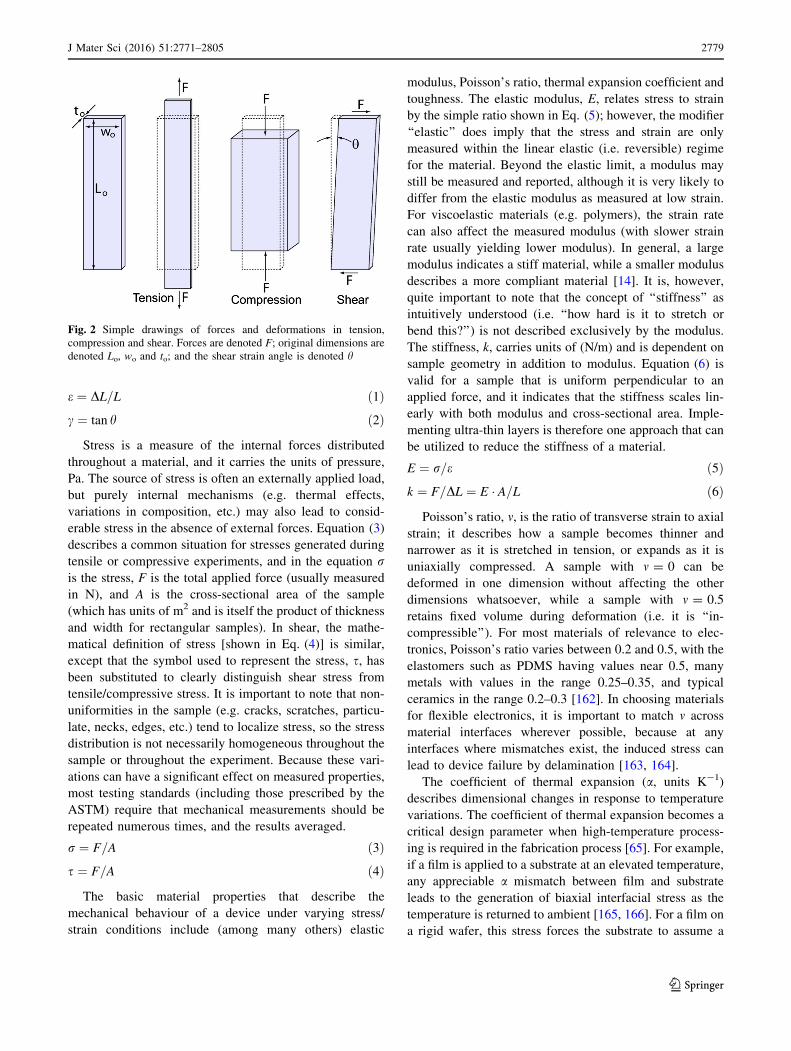
e ¼ DL=L ð1Þc ¼ tan h ð2Þ
Stress is a measure of the internal forces distributed
throughout a material, and it carries the units of pressure,
Pa. The source of stress is often an externally applied load,
but purely internal mechanisms (e.g. thermal effects,
variations in composition, etc.) may also lead to consid-
erable stress in the absence of external forces. Equation (3)
describes a common situation for stresses generated during
tensile or compressive experiments, and in the equation ris the stress, F is the total applied force (usually measured
in N), and A is the cross-sectional area of the sample
(which has units of m2 and is itself the product of thickness
and width for rectangular samples). In shear, the mathe-
matical definition of stress [shown in Eq. (4)] is similar,
except that the symbol used to represent the stress, s, hasbeen substituted to clearly distinguish shear stress from
tensile/compressive stress. It is important to note that non-
uniformities in the sample (e.g. cracks, scratches, particu-
late, necks, edges, etc.) tend to localize stress, so the stress
distribution is not necessarily homogeneous throughout the
sample or throughout the experiment. Because these vari-
ations can have a significant effect on measured properties,
most testing standards (including those prescribed by the
ASTM) require that mechanical measurements should be
repeated numerous times, and the results averaged.
r ¼ F=A ð3Þs ¼ F=A ð4Þ
The basic material properties that describe the
mechanical behaviour of a device under varying stress/
strain conditions include (among many others) elastic
modulus, Poisson’s ratio, thermal expansion coefficient and
toughness. The elastic modulus, E, relates stress to strain
by the simple ratio shown in Eq. (5); however, the modifier
‘‘elastic’’ does imply that the stress and strain are only
measured within the linear elastic (i.e. reversible) regime
for the material. Beyond the elastic limit, a modulus may
still be measured and reported, although it is very likely to
differ from the elastic modulus as measured at low strain.
For viscoelastic materials (e.g. polymers), the strain rate
can also affect the measured modulus (with slower strain
rate usually yielding lower modulus). In general, a large
modulus indicates a stiff material, while a smaller modulus
describes a more compliant material [14]. It is, however,
quite important to note that the concept of ‘‘stiffness’’ as
intuitively understood (i.e. ‘‘how hard is it to stretch or
bend this?’’) is not described exclusively by the modulus.
The stiffness, k, carries units of (N/m) and is dependent on
sample geometry in addition to modulus. Equation (6) is
valid for a sample that is uniform perpendicular to an
applied force, and it indicates that the stiffness scales lin-
early with both modulus and cross-sectional area. Imple-
menting ultra-thin layers is therefore one approach that can
be utilized to reduce the stiffness of a material.
E ¼ r=e ð5Þk ¼ F=DL ¼ E � A=L ð6Þ
Poisson’s ratio, m, is the ratio of transverse strain to axial
strain; it describes how a sample becomes thinner and
narrower as it is stretched in tension, or expands as it is
uniaxially compressed. A sample with m = 0 can be
deformed in one dimension without affecting the other
dimensions whatsoever, while a sample with m = 0.5
retains fixed volume during deformation (i.e. it is ‘‘in-
compressible’’). For most materials of relevance to elec-
tronics, Poisson’s ratio varies between 0.2 and 0.5, with the
elastomers such as PDMS having values near 0.5, many
metals with values in the range 0.25–0.35, and typical
ceramics in the range 0.2–0.3 [162]. In choosing materials
for flexible electronics, it is important to match m across
material interfaces wherever possible, because at any
interfaces where mismatches exist, the induced stress can
lead to device failure by delamination [163, 164].
The coefficient of thermal expansion (a, units K-1)
describes dimensional changes in response to temperature
variations. The coefficient of thermal expansion becomes a
critical design parameter when high-temperature process-
ing is required in the fabrication process [65]. For example,
if a film is applied to a substrate at an elevated temperature,
any appreciable a mismatch between film and substrate
leads to the generation of biaxial interfacial stress as the
temperature is returned to ambient [165, 166]. For a film on
a rigid wafer, this stress forces the substrate to assume a
Fig. 2 Simple drawings of forces and deformations in tension,
compression and shear. Forces are denoted F; original dimensions are
denoted Lo, wo and to; and the shear strain angle is denoted h
J Mater Sci (2016) 51:2771–2805 2779
123
dome shape described by the Stoney equation [167]. On the
other hand, for compliant substrates that are amenable to
flexible electronics, interfacial stress tends to promote
cylindrical rolling [65, 166], with radius of curvature, R,
described by [168]
R ¼ Est2s
6 1� mð Þ af � asð ÞDTEf tf
1� Ef t2f
Est2s
� �2
þ4 Ef tfEsts
1þ tfts
� �2
1þ tfts
� �264
375
ð7Þ
In Eq. (7), the subscripts ‘‘f’’ and ‘‘s’’ indicate, respec-
tively, the parameters associated with the film and sub-
strate, t and DT represent, respectively, thickness and the
change in temperature, and the Poisson’s ratio (m) is
assumed to be the same for film and substrate. The tem-
perature-induced curvature, together with the tendency of
typical substrate materials to shrink at moderate processing
temperatures, has the potential to lead to overlay errors as
different layers in a device stack are deposited [65, 166].
Toughness quantifies a material’s ability to resist failure.
It is measured by integrating the stress–strain curve between
zero strain and the strain at failure, and the units describe
the quantity of energy absorbed at failure per unit volume,
or (J/m3) [162]. ‘‘Fracture toughness’’ is an entirely distinct
parameter that describes a material’s resistance to crack
propagation and brittle fracture. It is also closely related to
‘‘tear-resistance’’, which is a key characteristic in the
longevity of thin, sheet-like flexible electronics. The pres-
ence of cracks leads to local concentration of stress at the
crack tip, and a ‘‘stress intensity factor’’, K (units MPa m1/
2), relates applied stress to the concentrated stress at the
crack tip. Unstable crack growth occurs when K reaches a
critical value, and the magnitude of this critical value is the
fracture toughness, Kc. Metals tend to have good fracture
toughness ([20 MPa m1/2) and generally fail by ductile
fracture, while oxides (\5 MPa m1/2) and glassy polymers
(\2 MPa m1/2) have low fracture toughness and tend to fail
by brittle fracture [162].
Finally, it is important to note that most mechanical
parameters are not actually fixed quantities, but instead
variables that respond to a wide range of conditions. All of
the parameters noted above, for instance, are temperature
dependent, and many parameters also vary with strain,
strain rate, strain history, thermal history and composition
of the environment. Small sample-to-sample variations can
also lead to differences in measured properties, and there-
fore testing of multiple samples is typically recommended.
Film failure by cracking or delamination
The durability of flexible electronic devices under strain
depends strongly upon crack formation/propagation [63,
169] and interfacial delamination [170], as these are the
two key mechanisms by which devices fail in response to
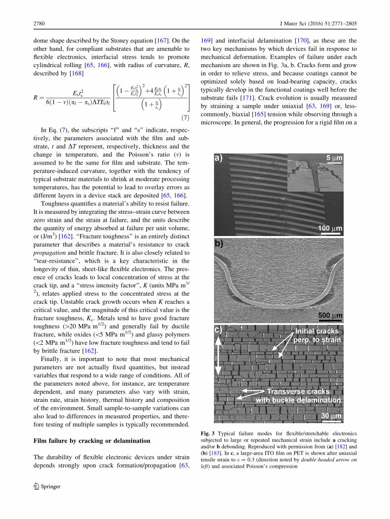
mechanical deformation. Examples of failure under each
mechanism are shown in Fig. 3a, b. Cracks form and grow
in order to relieve stress, and because coatings cannot be
optimized solely based on load-bearing capacity, cracks
typically develop in the functional coatings well before the
substrate fails [171]. Crack evolution is usually measured
by straining a sample under uniaxial [63, 169] or, less-
commonly, biaxial [165] tension while observing through a
microscope. In general, the progression for a rigid film on a
Fig. 3 Typical failure modes for flexible/stretchable electronics
subjected to large or repeated mechanical strain include a cracking
and/or b debonding. Reproduced with permission from (a) [182] and(b) [183]. In c, a large-area ITO film on PET is shown after uniaxial
tensile strain to e = 0.3 (direction noted by double-headed arrow on
left) and associated Poisson’s compression
2780 J Mater Sci (2016) 51:2771–2805
123
more compliant substrate is crack initiation, crack prop-
agation and crack densification (which includes a steady
reduction in crack spacing until saturation), followed by
transverse crack formation [172, 173]. A key measured
parameter is the crack onset strain or critical strain (eCO),which tends to decrease with increasing film thickness,
t [63, 174]. This behaviour is a result of the increasing
energy release rate with increasing film thickness, and the
classical scaling relationship has eCO varying with t-1/2
[63, 171, 175]. For brittle materials on more compliant
substrates (representing the vast majority of materials
systems for flexible electronics), cracks tend to initiate
around defect sites associated with surface irregularities in
the plastic substrate [63, 169]. This effect is generally
attributed to the concentration of stress at these surface
defects, and therefore increased eCO is often observed for
substrates with planarizing interlayers [63, 169]. Some
authors, however, attribute the increased eCO to defor-
mation in the interlayer [176, 177], while other groups
observe reduced eCO with the addition of a hardcoat and
attribute this to reduced adhesion between film and sub-
strate [178]. In any case, once cracks form in these brittle
films, they propagate rapidly through the entire thickness
of the coating and quickly extend large distances in a
direction perpendicular to the applied strain [169]. At the
substrate, the crack can also propagate along the coat-
ing/substrate interface (i.e. delamination), exacerbating
the failure process [171, 179]. With additional strain, new
cracks form and crack spacing decreases until a saturation
spacing is reached [172, 173, 180], and with continued
strain, transverse cracking and delamination of the frag-
ments may also occur [63, 172, 173, 181]. In Fig. 3c, a
strained ITO film on PET illustrates the microscopic
appearance of several of these cracking and delamination
phenomena.
The mismatching mechanical properties for compliant
substrate/stiff electronics systems also creates considerable
potential for device failure by delamination [184]. Under
strain, mismatching properties (a, m, E, etc.) lead to stresses
that act directly on the interface, and if the interfacial
toughness is low (i.e. poor adhesion), then debonding can
occur. Generally, as interfacial stress increases, films will
first slip a small distance with respect to the substrate
(*lm), before beginning the process of complete delam-
ination [182, 184]. It should also be noted that interfacial
slipping or delamination are not necessarily restricted to
the interface between the substrate and its immediate
overlayer. Delamination or interfacial slip may occur at
any interface in the device stack where the adhesion is
poor, and cohesive failure, in which internal cracks in the
plane of the film are responsible for debonding, has also
been observed (e.g. for P3HT/PCBM photovoltaic devices)
[185, 186].
Mechanics of bending-mode deformation
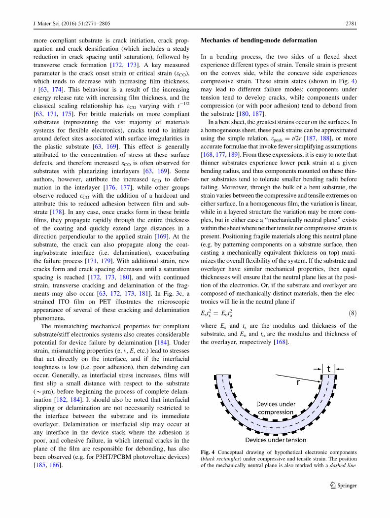
In a bending process, the two sides of a flexed sheet
experience different types of strain. Tensile strain is present
on the convex side, while the concave side experiences
compressive strain. These strain states (shown in Fig. 4)
may lead to different failure modes: components under
tension tend to develop cracks, while components under
compression (or with poor adhesion) tend to debond from
the substrate [180, 187].
In a bent sheet, the greatest strains occur on the surfaces. In
a homogeneous sheet, these peak strains can be approximated
using the simple relation, epeak = t/2r [187, 188], or more
accurate formulae that invoke fewer simplifying assumptions
[168, 177, 189]. From these expressions, it is easy to note that
thinner substrates experience lower peak strain at a given
bending radius, and thus components mounted on these thin-
ner substrates tend to tolerate smaller bending radii before
failing. Moreover, through the bulk of a bent substrate, the
strain varies between the compressive and tensile extremes on
either surface. In a homogeneous film, the variation is linear,
while in a layered structure the variation may be more com-
plex, but in either case a ‘‘mechanically neutral plane’’ exists
within the sheetwhere neither tensile nor compressive strain is
present. Positioning fragile materials along this neutral plane
(e.g. by patterning components on a substrate surface, then
casting a mechanically equivalent thickness on top) maxi-
mizes the overall flexibility of the system. If the substrate and
overlayer have similar mechanical properties, then equal
thicknesses will ensure that the neutral plane lies at the posi-
tion of the electronics. Or, if the substrate and overlayer are
composed of mechanically distinct materials, then the elec-
tronics will lie in the neutral plane if
Est2s ¼ Eot
2o ð8Þ
where Es and ts are the modulus and thickness of the
substrate, and Eo and to are the modulus and thickness of
the overlayer, respectively [168].
Fig. 4 Conceptual drawing of hypothetical electronic components
(black rectangles) under compressive and tensile strain. The position
of the mechanically neutral plane is also marked with a dashed line
J Mater Sci (2016) 51:2771–2805 2781
123
A number of other analytical models have been devel-
oped to describe flexible devices under deformation. For
example, Wu et al. modelled a three-layer system (con-
sisting of a flexible substrate, an adhesive layer and an
inorganic thin film) as elastic beams to determine how the
properties of the adhesive could be varied to minimize the
film strain during bending [190].
Mechanics of stretching-mode deformation
Because the neutral mechanical plane concept cannot be
used to protect brittle components in a stretching-mode
process, stretchability is generally considerably more dif-
ficult to engineer into an electronic system than bendabil-
ity. Most methods of designing stretchability are
implemented by avoiding straight paths in favour of
meandering patterns wherever possible [5]. For electronic
films restricted to the surface of a planar substrate, netlike
[10, 191], meandering [112, 192–196], and even multi-
level or fractal layouts [102, 197, 198] can be used to
improve stretchability. These layouts always have longer
electrical path lengths, but due to the influence of contact
resistance, the overall increase in electrical resistance may
not be substantial. Meandering conductors do, on the other
hand, allow the pattern to twist or ‘‘unfold’’ with applied
strain, thereby accommodating considerably greater strains
than materials patterned along a straight line.
Another well-known method for engineering stretcha-
bility is through the formation of buckled morphologies
that convert macroscopic stretching into local bending
deformations. To implement the technique, compliant
substrates are pre-strained in tension (in either 1D or 2D),
then the electronic films are deposited and the pre-strain is
released [89, 191, 199–206]. Because the films are gener-
ally stiffer than the substrates, they buckle out-of-plane
during relaxation, forming corrugations while bonded to
the substrate. In a pre-strain process, the buckling wave-
length, k, and amplitude, A, can be estimated by solving for
the minimum elastic energy to find the relations:
k ¼ 2ptEf 1� m2s� �
Es 1� m2f� �
" #1=3
ð9Þ
A ¼ t 4epreEf 1� m2s� �
3Es 1� m2f� �
" #2=3
�1
24
351=2
; ð10Þ
where t is the film thickness, epre is the pre-strain, Ef and Es
are the elastic moduli for film and substrate, and mf and msare the Poisson’s ratios for the film and substrate, respec-
tively. The use of these simple equations is widespread,
and some success in estimating the buckling geometry has
been achieved. The simple equations are, however,
imperfect in that estimated k and A values do not respond
well to variations in pre-strain. Because of this, the equa-
tions have also been modified to more accurately account
for the influence of pre-strain [100, 199, 205]:
k ¼ 2ptEf 1� m2s� �
Es 1� m2f� �
" #1=31
1þ epre� �
1þ nð Þ1=3ð11Þ
A ¼ t 4epreEf 1� m2s� �
3Es 1� m2f� �
" #2=3
�1
24
351=2
1
1þ epre� �1=2
1þ nð Þ1=3
ð12Þ
n ¼5epre 1þ epre
� �32
ð13Þ
Provided that the electronic films remain undamaged
throughout the buckling process [205], the materials are
subsequently able to ‘‘unbuckle’’ to accommodate stretch-
ing-mode strain that is less than the original pre-strain.
During unbuckling, the evolution of buckling wavelength
and amplitude can be calculated based on the theory
described by Jiang et al. [205].
Finite element analysis and materials models
Deriving analytical formulae that reliably describe
mechanical behaviours becomes increasingly difficult as
device complexity and strain increase. In order to predict
the behaviour of more complex architectures, a numerical
modelling technique known as finite element analysis
(FEA) can often be employed [207]. Finite element anal-
ysis is a valuable tool for mapping field variables such as
stress, strain and displacement that result when simulated
forces or deformations (compression, bending, stretching,
etc.) are applied to virtual models. In finite element anal-
ysis of a mechanical system, a body is discretized into a
collection of pieces called ‘‘elements’’, and analysis is
performed at ‘‘nodes’’ (which lie at the intersections
between elements). Solutions generally involve maps of
parameters of interest over the discretized body [208]. The
technique is extremely valuable both for exploring the
influence of design parameters (such as geometry and
material selections) over device behaviour and under-
standing the mechanisms of failure [178, 209].
Several software packages are utilized to implement
FEA, including both commercial programs (ANSYS,
Abaqus, etc.) and open-source freeware. In every case, the
basic procedural steps are equivalent: pre-processing
(which includes geometry construction, input of materials
properties and discretization of the model), analysis (in-
cluding tabulation and solution of relevant linear equa-
tions) and post-processing (display of solution). To
perform an analysis, a physical system is first approximated
2782 J Mater Sci (2016) 51:2771–2805
123
as a model with geometry defined either within the FEA
software or by importing from a separate computer-aided
design program. In many cases, geometric approximations
are utilized to reduce computation time, such as solving a
two-dimensional geometry when the system is not expec-
ted to vary in the third dimension.
The loading parameters and boundary conditions must
also be described within the model. Boundary conditions
may be expressed in terms of displacements (known as
‘‘essential boundary conditions’’) or forces (known as
‘‘natural boundary conditions’’). To match the reality of
tensile testing experiments, uniform strain is defined at one
end of a sample, while locking the displacement of the
opposing edge to zero [210]. To mimic bending experi-
ments, an out-of-plane displacement may be applied at one
end, while displacement at the opposite end is fixed to zero.
Once the basic geometry is defined, the model is divided
into discrete pieces during a process called ‘‘meshing’’.
Generally, the user manually defines an appropriate num-
ber of nodes/elements and chooses the element geometry.
The FEA software then distributes these elements using an
automated algorithm, ensuring that elements do not overlap
and positioning nodes wherever the elements meet. An N-
dimensional simulation (where N is the number of field
variables evaluated at a given point) with M nodes requires
M�N linear equations, and therefore choosing a reasonable
mesh size is an important design problem. Simulations with
more nodes/elements tend to more closely approximate the
correct solution, but are also more computationally inten-
sive (i.e. slower). Mesh size analysis should therefore
typically be performed to determine the maximum mesh
size for which the solution converges.
A plethora of element types are built into FEA software
packages, and most packages also allow custom elements.
Typical 2D mesh elements are triangular or quadrilateral in
shape (where each corner corresponds to a node) [210], and
3D mesh elements are typically based on either solid ele-
ments (which connect along faces and may also be called
brick elements) or shell elements (which connect along
edges). A combination of elements may also be utilized;
for example, Kim et al. used 4-node shell elements to
model a thin film on a substrate represented as an 8-node
brick element [211]. The values within an element may be
interpolated from those at the nodes using an appropriate
shape function for that particular element type.
Once the geometrical model is defined and meshed, the
key to FEA is logically interrelating forces, F, and dis-
placements, u, throughout the model to compile a set of
solvable equations. Forces in one direction can lead to node
displacements in any direction (cf., Poisson’s effect), so the
set of equations relating forces and displacements take the
general form:
Fi ¼Xj
kijuj; ð14Þ
where i and j each indicate combinations of both node and
direction, Fi are nodal forces in i, uj are displacements in j,
and kij are the stiffness coefficients relating Fi and uj. The
fundamental theory that is used to define the stiffness
coefficients, kij, is referred to as the ‘‘constitutive model’’
for the simulated material [212]. This model can be as
simple as inputting the elastic modulus and Poisson’s ratio
(i.e. a Hookean model); however, this is generally only
valid for very small deformations. Elastomeric materials
(such as PDMS) with moduli that vary as a function of
strain are more suitably represented utilizing non-linear
constitutive models, such as the Mooney–Rivlin hypere-
lastic model [212]. Metals are often modelled as plastically
deformable solids using a power law, in which stress is
related to strain by a hardening exponent, N, through the
equation r = KeN, where K is a prefactor [12]. Elastic–
plastic models, in which different constitutive equations are
applied below and above a defined transition point, may
also be implemented for materials that are strained beyond
their linear elastic range: for example, an elastic equation
may be applied below the limit, and a power law above it
[210]. Each material in the device stack can be expected to
have a different array of material parameters, and therefore
it is important to define an appropriate constitutive model
for each and every material in a flexible device.
In most FEA of solids, the solution is found by mini-
mizing the strain energy of the system: the set of equations
describes the strain energy density at each node, and the
optimum solution is the set of displacements (uj) that
minimizes the overall elastic energy [213]. From this
solution, field variables such as stresses and strains can be
calculated at the nodes, or with appropriate interpolation,
throughout the elements. Results can be exported in
tables or visualized in a variety of formats. While it is
relatively straightforward to generate a model and evaluate
a solution, demonstrating the validity of that model is more
challenging. The modeller should evaluate scenarios with
predictable outcomes and assess the logic of the generated
solution, and models should be validated through com-
parison with experimental data whenever possible.
To predict failure through delamination, adhesion at the
interface must be represented within the model. One
approach is to utilize cohesive zone elements, treating
delamination as a gradual separation of elements, and uti-
lizing a traction separation law to relate the separation
between nodes to a traction stress vector acting on those
nodes. Within such a model, the traction separation vector
increases to a critical value as the separation is increased,
beyond this value the traction decreases, describing a
J Mater Sci (2016) 51:2771–2805 2783
123
softening or (irreversible) degradation of the interface [210,
214, 215].
Mechanical characterization
Mechanical characterization techniques for flexible elec-
tronics applications can be sub-divided into two broad
categories: (i) tests to determine mechanical constants and
(ii) tests to track the evolution of device performance. The
former group primarily involves the application of well-
established mechanical characterization techniques, and
data analysis is performed by more or less conventional
means. Two well-known organizations, the American
Society for Testing and Materials (ASTM) and the Inter-
national Organization for Standardization (ISO), have
developed thousands of standardized testing procedures for
the repeatable characterization of a wide range of materials
and systems. Existing standards are periodically updated
and new standards are continuously added. Several stan-
dards are relevant to flexible electronic materials, and these
are cited throughout this section [216–224].
Information about the performance of electronic devices
under the influence of mechanical stresses or strains (i.e.
the second category above) is extracted by several tech-
niques, most of which involve measuring device perfor-
mance metrics during mechanical deformation processes.
In this review, we categorize these test procedures
according to the mode of mechanical deformation, and we
provide information in each category about the typical test
equipment, device applications and the results obtained for
the various classes of flexible electronic devices. Table 1
broadly summarizes this information by listing common
test procedures and dominant failure modes under each
type of deformation.
Determining materials constants
In order to describe a device in a finite element model or
with an analytical equation, the basic material properties
must first be known. A reasonable starting point is to utilize
bulk values that are either reported in the literature or
independently measured. These bulk properties are com-
monly measured using techniques such as tensile testing (in
which samples are stretched in tension while recording
stress and strain), dynamic mechanical analysis (in which a
configurable sinusoidal force is applied to generate a
sinusoidal stress–strain profile used to resolve the vis-
coelastic properties of the sample) or rheometry (for ultra-
soft samples, gels, pastes and liquids). Each of these
techniques can potentially be conducted over a range of
temperatures, both to characterize materials at application-
specific temperatures and also to determine glass transition
temperatures, Tg, below which a material is rigid and
glassy and above which a material is soft and rubbery.
The material properties for thin layers may, however,
differ from bulk values, as differences in thickness can lead
to microstructural variation [235]. Processing conditions
also have a strong influence over film structure, such that
different fabrication techniques may lead to materials with
different mechanical properties [236]. Mechanically char-
acterizing thin materials on a substrate is challenging, as
the overall mechanical behaviour is derived from a com-
bination of the properties of all the materials present.
Nanoindentation is one technique that can be used to probe
the properties of a thin film: this technique involves
depressing a piezoelectrically controlled indenter tip into
the surface of a material, while tracking the force/dis-
placement curve [177, 237, 238]. Loading and unloading
curves are collected, and provided that the shape of the
indenter tip is well known, both the hardness and modulus
may be calculated. The properties of the film can be ade-
quately distinguished from the substrate when (1) the
thickness of the film is at least ten times the indentation
depth, and (2) the substrate is substantially stiffer than the
film (to ensure that only the film deforms upon indentation)
[239].
Another useful technique for determining the moduli of
thin films on elastomeric substrates involves exploiting the
buckling behaviour of the film [54–56, 58, 240, 241]. In
Table 1 Mechanical deformation modes and their effect on the
materials/components in flexible electronics
Deformation
mode (or
testing
mode)
Failure modes and test procedures
Bending Delamination or slipping at hard/soft material
interfaces [184]
Cracking in functional coatings [165, 169, 171]
Modulation in semiconductor charge carrier mobility
[225, 226]
Stretching Delamination and slipping at hard/soft material
interfaces [184]
Cracking in functional coatings [171, 227]
Buckling of stiff functional materials on softer
substrates [205, 228]
ASTMstandard: tensile properties of plastic sheeting [224]
Twisting Buckling, delamination [229, 230]
ASTM standard: torsion test [223]
Impact ASTM standard: impact resistance of plastic sheeting [216]
Abrasion Tensile cracking, substrate gouging [231, 232]
ASTM standard: scratch resistance of plastics [222]
(Adhesion) Tape test [217], peel test [233], scratch test [233],
bend test [234]
2784 J Mater Sci (2016) 51:2771–2805
123
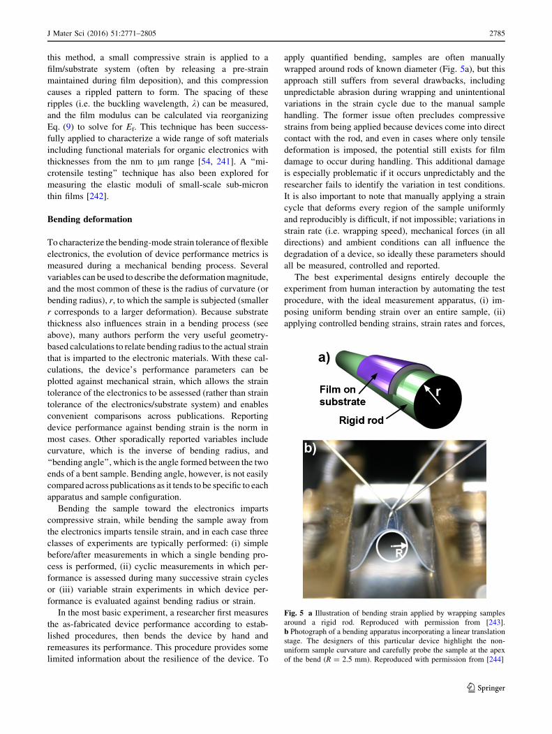
this method, a small compressive strain is applied to a
film/substrate system (often by releasing a pre-strain
maintained during film deposition), and this compression
causes a rippled pattern to form. The spacing of these
ripples (i.e. the buckling wavelength, k) can be measured,
and the film modulus can be calculated via reorganizing
Eq. (9) to solve for Ef. This technique has been success-
fully applied to characterize a wide range of soft materials
including functional materials for organic electronics with
thicknesses from the nm to lm range [54, 241]. A ‘‘mi-
crotensile testing’’ technique has also been explored for
measuring the elastic moduli of small-scale sub-micron
thin films [242].
Bending deformation
To characterize the bending-mode strain tolerance of flexible
electronics, the evolution of device performance metrics is
measured during a mechanical bending process. Several
variables can be used to describe the deformationmagnitude,
and the most common of these is the radius of curvature (or
bending radius), r, to which the sample is subjected (smaller
r corresponds to a larger deformation). Because substrate
thickness also influences strain in a bending process (see
above), many authors perform the very useful geometry-
based calculations to relate bending radius to the actual strain
that is imparted to the electronic materials. With these cal-
culations, the device’s performance parameters can be
plotted against mechanical strain, which allows the strain
tolerance of the electronics to be assessed (rather than strain
tolerance of the electronics/substrate system) and enables
convenient comparisons across publications. Reporting
device performance against bending strain is the norm in
most cases. Other sporadically reported variables include
curvature, which is the inverse of bending radius, and
‘‘bending angle’’, which is the angle formed between the two
ends of a bent sample. Bending angle, however, is not easily
compared across publications as it tends to be specific to each
apparatus and sample configuration.
Bending the sample toward the electronics imparts
compressive strain, while bending the sample away from
the electronics imparts tensile strain, and in each case three
classes of experiments are typically performed: (i) simple
before/after measurements in which a single bending pro-
cess is performed, (ii) cyclic measurements in which per-
formance is assessed during many successive strain cycles
or (iii) variable strain experiments in which device per-
formance is evaluated against bending radius or strain.
In the most basic experiment, a researcher first measures
the as-fabricated device performance according to estab-
lished procedures, then bends the device by hand and
remeasures its performance. This procedure provides some
limited information about the resilience of the device. To
apply quantified bending, samples are often manually
wrapped around rods of known diameter (Fig. 5a), but this
approach still suffers from several drawbacks, including
unpredictable abrasion during wrapping and unintentional
variations in the strain cycle due to the manual sample
handling. The former issue often precludes compressive
strains from being applied because devices come into direct
contact with the rod, and even in cases where only tensile
deformation is imposed, the potential still exists for film
damage to occur during handling. This additional damage
is especially problematic if it occurs unpredictably and the
researcher fails to identify the variation in test conditions.
It is also important to note that manually applying a strain
cycle that deforms every region of the sample uniformly
and reproducibly is difficult, if not impossible; variations in
strain rate (i.e. wrapping speed), mechanical forces (in all
directions) and ambient conditions can all influence the
degradation of a device, so ideally these parameters should
all be measured, controlled and reported.
The best experimental designs entirely decouple the
experiment from human interaction by automating the test
procedure, with the ideal measurement apparatus, (i) im-
posing uniform bending strain over an entire sample, (ii)
applying controlled bending strains, strain rates and forces,
Fig. 5 a Illustration of bending strain applied by wrapping samples
around a rigid rod. Reproduced with permission from [243].
b Photograph of a bending apparatus incorporating a linear translation
stage. The designers of this particular device highlight the non-
uniform sample curvature and carefully probe the sample at the apex
of the bend (R = 2.5 mm). Reproduced with permission from [244]
J Mater Sci (2016) 51:2771–2805 2785
123
(iii) minimizing contact with the sample and (iv) auto-
matically measuring and calculating all relevant device
performance parameters in situ. It is difficult to design
equipment with all of these in mind, but several devices
certainly deliver more reliable data than manual wrapping
experiments. One of the most common mechanized
approaches is to affix the two ends of a substrate to plates
on a translation stage [187]. An image illustrating this
scheme is shown in Fig. 5b, and from the image it can be
inferred that greater bending strains are applied as the
plates are brought closer together. This approach is
advantageous because the experimenter does not neces-
sarily handle the sample during testing, but care must still
be taken to ensure that the strain cycles are reproducible. It
must also be understood that with this apparatus, bending
strain is not uniform over the entire sample, and the
maximum strain is only applied at the apex of the bend. To
address this, some apparatuses implement an arc-like
(rather than linear) motion [245], while others roll samples
around a mandrel of known diameter [227].
Abrasion-induced degradation at electrical contacts also
represents a considerable problem, and it is very likely that
many efforts to address this practical issue are not reported.
Minimizing motion at all points of contact is the best
approach, but metallic lubricants, such as eGaIn, have also
been added at the contacts to reduce abrasion by the
electrical probes [226].
Bending-mode tests to evaluate the strain tolerance of
flexible electronics are widespread in the literature, and
plots of device-specific performance metrics during bend-
ing deformations have been published for most materials
and devices. These include, for instance, insulators and
barrier layers [246, 247], electrical conductors [152, 248–
254] and transparent conductors. When discussing trans-
parent conductors, common themes include tracking the
mechanical degradation of the brittle transparent conduct-
ing oxides (especially ITO) [64, 227, 255–261] or devel-
oping more strain-tolerant alternatives [28, 243, 256, 261–
281]. Numerous transparent conductors that outperform
ITO from a strain tolerance standpoint have now been
described, although it is interesting that few comparisons of
bending-induced failure among the different classes of non-
TCO materials have appeared to date. In addition to elec-
trical conductivity, transparent conductors must also exhibit
light transmission, yet measurements of bending-mode
strain tolerance usually neglect optical properties. Light
transmission and transparent conductor figures-of-merit
during strain cycling are generally not discussed, and this is
likely due to the difficultly in aligning optical components
within a mechanical bending apparatus and synchronizing
light transmission measurements with the strain cycle.
Another class of devices that is highly relevant for
flexible electronics is thin-film transistors, and numerous
bending-mode deformation studies have now been com-
pleted for these devices [73, 189, 225, 226, 244, 282–297].
One common observation is charge carrier mobility that
decreases as devices are bent in one direction (i.e. ten-
sion/compression), but increases when bent in the opposite.
The direction of response, however, is not consistent across
all semiconductor/dielectric pairs, and the effect has been
attributed to strain-induced variations in the electron
orbitals at the interface [226]. Sekitani et al. perform
extensive mechanical testing on pentacene-based FETs
positioned in a neutral mechanical plane, including cyclic
testing to 160,000 bending cycles [225], and in a separate
publication [283], the minimum bending radii that various
TFT materials systems endure before failure are cata-
logued. These authors (and others) [292] also note that the
direction of strain with respect to the semiconducting
channel plays a role in determining strain tolerance.
Bending-mode deformation studies have also been
completed on flexible solar cells [243, 298–300]; however,
incident light power profiles tend to complicate the inves-
tigation of bending-mode strain tolerance. The spatial
power distribution for most solar simulators is calibrated to
uniformly deliver 100 mW/cm2 at a fixed measurement
plane. As samples are bent out of this fixed plane, the
spatial and/or spectral power distribution may depart
somewhat from that of the typical measurement plane.
Moreover, the solid angle for light absorption, wave-
guiding and reflected power all vary with the light inci-
dence angle, and these effects collectively lead to some
uncertainty in the measured performance metrics for solar
cells. To address this issue, researchers may accept the
uncertainty [298, 299], return the device to the flattened
state before conducting the solar cell evaluation [243] or
perform cyclic testing at various radii [299].
Experiments to track the evolution of device performance
parameters during bending have also been published for
passive capacitors and inductors [301], supercapacitor sys-
tems [302–306], energy scavengers [2, 307, 308], batteries
[309–319], light-emitting devices [264, 320–327], memory
devices [328–345], touch screens/pressure sensors [346–
349], antennas [350, 351], waveguides [352] and other
electronic circuits [200, 283, 295, 353]. Overall, bending is
an extremely important deformation mode that must be fully
characterized to facilitate the development of reliable flexi-
ble electronic devices. Both the characteristics of individual
components and integrated systems must be considered.
Stretching deformation
In a stretching-mode measurement, the performance
parameters for the electronic device under test are contin-
uously or periodically recorded during tensile strain pro-
cesses, and three basic types of measurements are common:
2786 J Mater Sci (2016) 51:2771–2805
123
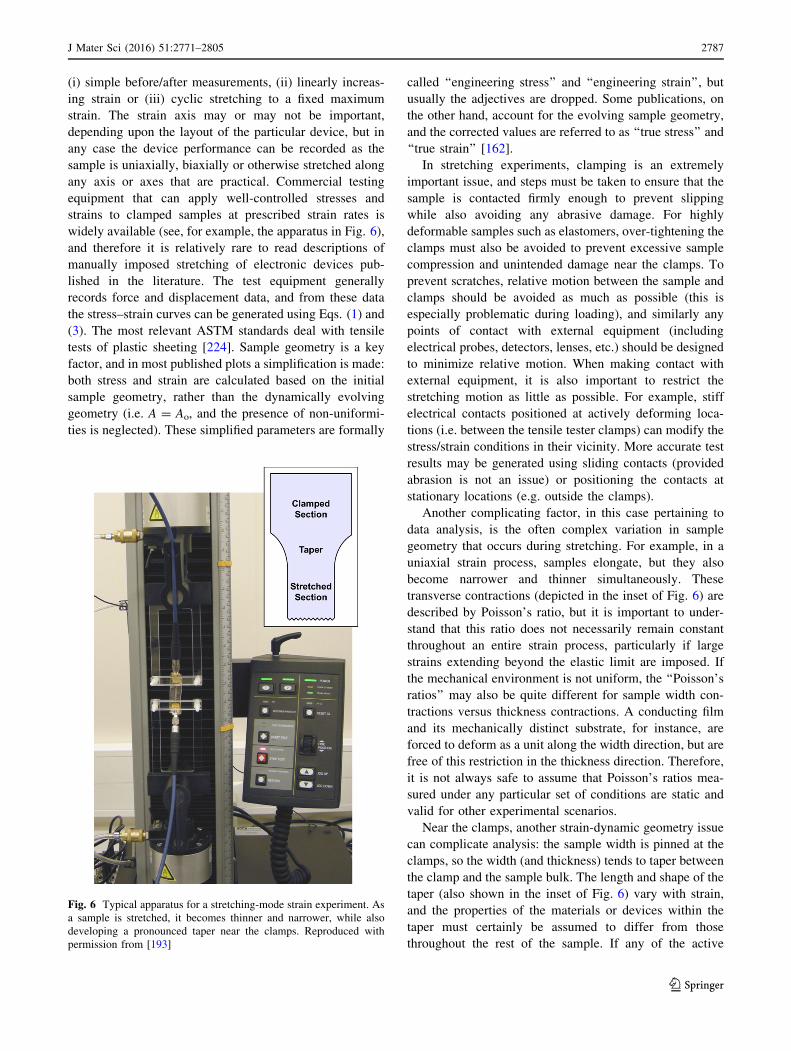
(i) simple before/after measurements, (ii) linearly increas-
ing strain or (iii) cyclic stretching to a fixed maximum
strain. The strain axis may or may not be important,
depending upon the layout of the particular device, but in
any case the device performance can be recorded as the
sample is uniaxially, biaxially or otherwise stretched along
any axis or axes that are practical. Commercial testing
equipment that can apply well-controlled stresses and
strains to clamped samples at prescribed strain rates is
widely available (see, for example, the apparatus in Fig. 6),
and therefore it is relatively rare to read descriptions of
manually imposed stretching of electronic devices pub-
lished in the literature. The test equipment generally
records force and displacement data, and from these data
the stress–strain curves can be generated using Eqs. (1) and
(3). The most relevant ASTM standards deal with tensile
tests of plastic sheeting [224]. Sample geometry is a key
factor, and in most published plots a simplification is made:
both stress and strain are calculated based on the initial
sample geometry, rather than the dynamically evolving
geometry (i.e. A = Ao, and the presence of non-uniformi-
ties is neglected). These simplified parameters are formally
called ‘‘engineering stress’’ and ‘‘engineering strain’’, but
usually the adjectives are dropped. Some publications, on
the other hand, account for the evolving sample geometry,
and the corrected values are referred to as ‘‘true stress’’ and
‘‘true strain’’ [162].
In stretching experiments, clamping is an extremely
important issue, and steps must be taken to ensure that the
sample is contacted firmly enough to prevent slipping
while also avoiding any abrasive damage. For highly
deformable samples such as elastomers, over-tightening the
clamps must also be avoided to prevent excessive sample
compression and unintended damage near the clamps. To
prevent scratches, relative motion between the sample and
clamps should be avoided as much as possible (this is
especially problematic during loading), and similarly any
points of contact with external equipment (including
electrical probes, detectors, lenses, etc.) should be designed
to minimize relative motion. When making contact with
external equipment, it is also important to restrict the
stretching motion as little as possible. For example, stiff
electrical contacts positioned at actively deforming loca-
tions (i.e. between the tensile tester clamps) can modify the
stress/strain conditions in their vicinity. More accurate test
results may be generated using sliding contacts (provided
abrasion is not an issue) or positioning the contacts at
stationary locations (e.g. outside the clamps).
Another complicating factor, in this case pertaining to
data analysis, is the often complex variation in sample
geometry that occurs during stretching. For example, in a
uniaxial strain process, samples elongate, but they also
become narrower and thinner simultaneously. These
transverse contractions (depicted in the inset of Fig. 6) are
described by Poisson’s ratio, but it is important to under-
stand that this ratio does not necessarily remain constant
throughout an entire strain process, particularly if large
strains extending beyond the elastic limit are imposed. If
the mechanical environment is not uniform, the ‘‘Poisson’s
ratios’’ may also be quite different for sample width con-
tractions versus thickness contractions. A conducting film
and its mechanically distinct substrate, for instance, are
forced to deform as a unit along the width direction, but are
free of this restriction in the thickness direction. Therefore,
it is not always safe to assume that Poisson’s ratios mea-
sured under any particular set of conditions are static and
valid for other experimental scenarios.
Near the clamps, another strain-dynamic geometry issue
can complicate analysis: the sample width is pinned at the
clamps, so the width (and thickness) tends to taper between
the clamp and the sample bulk. The length and shape of the
taper (also shown in the inset of Fig. 6) vary with strain,
and the properties of the materials or devices within the
taper must certainly be assumed to differ from those
throughout the rest of the sample. If any of the active
Fig. 6 Typical apparatus for a stretching-mode strain experiment. As
a sample is stretched, it becomes thinner and narrower, while also
developing a pronounced taper near the clamps. Reproduced with
permission from [193]
J Mater Sci (2016) 51:2771–2805 2787
123
components are located within this tapered region, data
analysis could become considerably more complicated than
expected, and therefore it is best to keep all active materials
far from the clamps wherever possible. If this cannot be
avoided (such as for analysis of films or devices that extend
through the clamps), then the sample length should be as
large as is practical to reduce the influence of this tapered
region.
If the sample is mechanically inhomogeneous (even if
by design), then it is quite possible that behaviour under
strain could be even more unpredictable. For example, a
material comprising distinct stiff and compliant sections
will preferentially deform in the most compliant regions. In
this case, in situ microscopy or finite element models may
be necessary to truly understand the geometry over the
entire sample. All of these geometry issues highlight the
importance of rationally considering the evolution of
sample geometry and understanding how it influences the
analysis. In some cases, geometric variations will be lar-
gely irrelevant. This could include evaluation of ‘‘com-
plete’’ electronic circuits by tracking a particular electrical
signal during strain. If the important parameters are
entirely independent of geometry, then it may not be nec-
essary to understand that geometry in great detail. On the
other hand, if geometric parameters are used anywhere in
the analysis (e.g. in the calculations of power conversion
efficiency in a solar cell, charge carrier mobility in a
transistor or resistivity in an electrical conductor), then it
may be critically important to directly track the dimensions
of the sample or devices throughout the stretching experi-
ment and use only these measured dimensions for all
calculations.
A host of flexible electronic materials and devices have
been evaluated in stretching-mode experiments. Extensive
tests of strain tolerance have, for example, been performed
on electrical conductors [15, 16, 71, 72, 123, 152, 192–194,
197, 248–251, 320, 354–363]. Among these publications,
Graz et al. performed an extended study of homogeneous
gold thin films under cyclic strain [362], and extensive
studies of conductors patterned in a strain-tolerant mean-
dering patterns were performed by Bossuyt et al. and Hsu
et al. [192, 194]. Stretching-mode strain tolerance has also
been evaluated for a wide range of transparent conductors
[163, 173, 227, 243, 262, 269, 305, 346, 364–367]. Most
studies tend to report the increase in raw electrical resis-
tance with strain, although some include geometrical
analysis and report the evolution of sheet resistance or
resistivity [163, 359, 366]. The most complete strain tol-
erance studies tend to focus on ITO [173, 227, 368], and
the degradation of this material under uniaxial strain is
becoming well understood. In recent publications, how-
ever, a common theme is the development of new trans-
parent conductors with strain tolerance considerably
superior to ITO. This has certainly been accomplished,
although few side-by-side comparisons among the more
strain-tolerant materials have yet been published [367].
Most studies also note that electrical degradation of
transparent conductors is more problematic than optical
degradation and do not address the variation in light
transmission that occurs during strain. Against this trend,
one publication demonstrates improved transmission for a
stretched Au nanomesh [269], and two others report the
evolution of transparent conductor sheet resistance, trans-
mission and figure-of-merit [366, 369].
Several examples of complete stretchable electronic
devices tested under uniaxial strain have also been reported
in the literature. These include published plots of device-
specific performance parameters for stretchable solar cells
[55, 240, 370–373], thin-film transistors [73, 285, 360,
374–378], diodes [202, 375], capacitors [81, 123, 354,
365], supercapacitors [304, 305, 379–385], batteries [102,
386–390], mechanical energy harvesters [391], light-emit-
ting devices [3, 249, 359, 361, 392], antennas [17, 18, 197,
393–399], electronic circuits [4, 112, 200, 211, 400] and
biomedical devices [109]. Kaltenbrunner et al. [370] per-
formed uniaxial, biaxial and cyclic stretching strain toler-
ance studies for P3HT:PCBM solar cells fabricated on
extremely thin plastic substrates, and Lipomi et al. [240]
published an excellent mechanical study showcasing solar
cells formed using strain-tolerant electrodes and two dif-
ferent photoactive compositions. In each publication,
photovoltaic performance metrics were recorded during
various strain processes, and the authors focussed their
discussion on mechanisms leading toward strain tolerance.
For TFTs, some of the trends noted in bending mode have
been reproduced in stretching experiments. This includes
carrier mobility that linearly increases/decreases with strain
and partially recovers with relaxation [285]. Gaikwad et al.
[386] published current/voltage characteristics, impedance/
frequency maps and electrical discharge curves for
stretchable batteries under several strain conditions, and
Liang et al. [392] showed plots of current density, lumi-
nance and efficiency versus tensile strain up to 120 % for
stretchable OLEDs on polyurethane acrylate substrates.
Kubo et al. [18] characterized RF antennas under stretch-
ing-mode strain by reporting reflected power and resonant
frequency for both linearly increasing and cyclic tensile
strains up to 120 %, and Kim et al. [200] formed stretch-
able ring oscillator and differential amplifier circuitry and
recorded the variation in voltage outputs under various
strain conditions.
Variations in device performance as a function of
deformation have further been exploited to engineer strain
sensors that can withstand much larger deformations than
traditional inorganic devices [10, 17, 115, 123, 126, 153,
354, 365, 393, 396, 401]. These flexible strain and pressure
2788 J Mater Sci (2016) 51:2771–2805
123
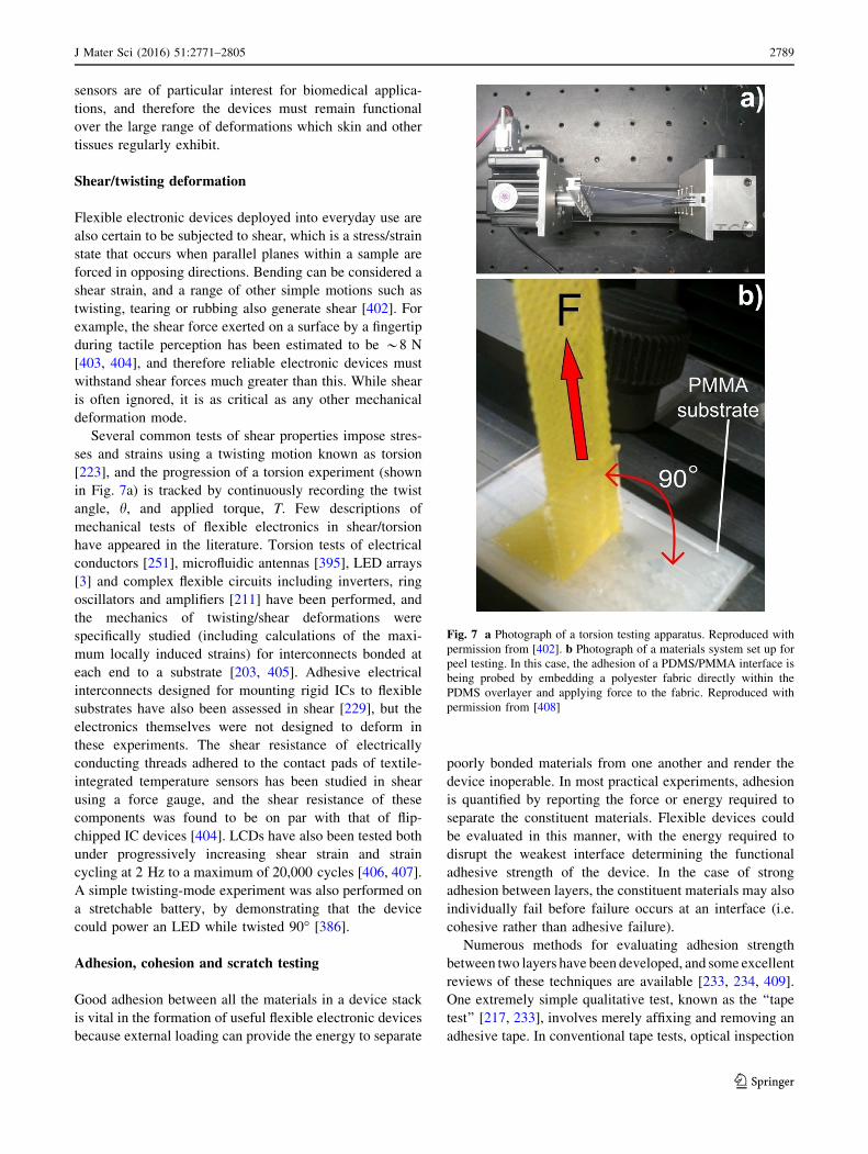
sensors are of particular interest for biomedical applica-
tions, and therefore the devices must remain functional
over the large range of deformations which skin and other
tissues regularly exhibit.
Shear/twisting deformation
Flexible electronic devices deployed into everyday use are
also certain to be subjected to shear, which is a stress/strain
state that occurs when parallel planes within a sample are
forced in opposing directions. Bending can be considered a
shear strain, and a range of other simple motions such as
twisting, tearing or rubbing also generate shear [402]. For
example, the shear force exerted on a surface by a fingertip
during tactile perception has been estimated to be *8 N
[403, 404], and therefore reliable electronic devices must
withstand shear forces much greater than this. While shear
is often ignored, it is as critical as any other mechanical
deformation mode.
Several common tests of shear properties impose stres-
ses and strains using a twisting motion known as torsion
[223], and the progression of a torsion experiment (shown
in Fig. 7a) is tracked by continuously recording the twist
angle, h, and applied torque, T. Few descriptions of
mechanical tests of flexible electronics in shear/torsion
have appeared in the literature. Torsion tests of electrical
conductors [251], microfluidic antennas [395], LED arrays
[3] and complex flexible circuits including inverters, ring
oscillators and amplifiers [211] have been performed, and
the mechanics of twisting/shear deformations were
specifically studied (including calculations of the maxi-
mum locally induced strains) for interconnects bonded at
each end to a substrate [203, 405]. Adhesive electrical
interconnects designed for mounting rigid ICs to flexible
substrates have also been assessed in shear [229], but the
electronics themselves were not designed to deform in
these experiments. The shear resistance of electrically
conducting threads adhered to the contact pads of textile-
integrated temperature sensors has been studied in shear
using a force gauge, and the shear resistance of these
components was found to be on par with that of flip-
chipped IC devices [404]. LCDs have also been tested both
under progressively increasing shear strain and strain
cycling at 2 Hz to a maximum of 20,000 cycles [406, 407].
A simple twisting-mode experiment was also performed on
a stretchable battery, by demonstrating that the device
could power an LED while twisted 90� [386].
Adhesion, cohesion and scratch testing
Good adhesion between all the materials in a device stack
is vital in the formation of useful flexible electronic devices
because external loading can provide the energy to separate
poorly bonded materials from one another and render the
device inoperable. In most practical experiments, adhesion
is quantified by reporting the force or energy required to
separate the constituent materials. Flexible devices could
be evaluated in this manner, with the energy required to
disrupt the weakest interface determining the functional
adhesive strength of the device. In the case of strong
adhesion between layers, the constituent materials may also
individually fail before failure occurs at an interface (i.e.
cohesive rather than adhesive failure).
Numerous methods for evaluating adhesion strength
between two layers have been developed, and some excellent
reviews of these techniques are available [233, 234, 409].
One extremely simple qualitative test, known as the ‘‘tape
test’’ [217, 233], involves merely affixing and removing an
adhesive tape. In conventional tape tests, optical inspection
Fig. 7 a Photograph of a torsion testing apparatus. Reproduced with
permission from [402]. b Photograph of a materials system set up for
peel testing. In this case, the adhesion of a PDMS/PMMA interface is
being probed by embedding a polyester fabric directly within the
PDMS overlayer and applying force to the fabric. Reproduced with
permission from [408]
J Mater Sci (2016) 51:2771–2805 2789
123
is used to determine if the film remains intact following the
test, but for functional electronics, before/after or cyclic
measurements of device-specific performance parameters
can also be recorded. These simple tape tests have been
performed on various flexible conductors [250, 253, 254,
320], transparent conductors [26, 261, 265, 268, 270, 410–
412], fuel cell membranes [412] and batteries [413]. These
tape tests are useful, yet they are also highly qualitative: no
numerical values for adhesion are obtained, the tests results
cannot generally be compared from publication-to-publica-
tion (or even from experimenter-to-experimenter), and the
tests are limited to investigating adhesive strengths less than
that between the tape and film (which could itself vary with
the type of tape utilized).
Other, more quantitative tests are available, and these
have been used to determine thin-film adhesion for a variety
of materials. Peel testing is a mechanized variation of the
tape test used to quantify adhesive forces [233, 234]. In this
test, the adhesive tape (or even the film itself) is attached to
a motor and load cell, and a mechanical force is applied
while the opposing material is held firmly in place. As the
two materials of interest are separated, force/displacement
data are recorded. In Fig. 7b, a peel test is shown with a
tensile tester physically pulling on a piece of fabric (yellow
colour) embedded in a PDMS film; strong adhesion
between the fabric and the film is critical for achieving
quantitative measurements. Most of the disadvantages
inherent to manual tape tests (noted above) remain in place,
but quantitative data can be collected [414]. Several sub-
strates with surface treatments intended to improve adhe-
sion of electronic materials have been assessed in peel tests
[415], as have transparent conductors [416], and complete
organic solar cells [417, 418]. The results of peel tests have
also been used to inform stretchable electronics numerical
modelling studies [183]. A ‘‘dual cantilever beam’’ mode
has also been used to reveal adhesion information [416–
418]. In this mode, a test sample is firmly affixed (with an
appropriate adhesive) between two plates, and these plates
are then separated while recording force/displacement data.
The test structure is forced to fail somewhere within the
device stack, and the force/displacement curve can be
analysed to determine failure energy. This technique has
been employed to measure adhesion/cohesion properties of
several solar cell architectures [416–418].
Scratch testing methods [218, 221, 222, 231–234] have
also been used to assess the interfacial strength of elec-
tronic materials. In these tests, a stylus is forced into
contact with the sample and translated across the surface,
inducing shear stress at the substrate/film interface. This
interface will fail if shear forces exceed a critical load
correlated with the interfacial strength, so in the most
useful scratch tests, the load is linearly increased during the
test in order to determine this critical load. The technique
has been criticized (primarily due to difficulties in accu-
rately identifying when failure occurs, and also in estab-
lishing reliable comparisons when different styluses or
substrates are utilized) [233], but it does remain a well-
established technique for evaluating adhesion. Several
examples of application to flexible electronics have been
published including evaluation of critical loads for several
transparent conductors [238, 346, 419–421], piezoelectric
transducers [420] and both semiconductors and dielectrics
for FETs [414, 415].
Observation and analysis of bending processes [185,
186, 234, 422, 423] has also been used to measure the
adhesion/cohesion of material sets intended for flexible
electronics. Generally, samples are deformed (often using a
four-point bend geometry) while collecting force/dis-
placement data, and post-analysis reveals parameters such
as critical loads for adhesive/cohesive failure and adhe-
sive/cohesive energy. Vibration [420], indentation [234,
238] and pulsed laser irradiation [181] have also been used
to induce failure in analyses of adhesive/cohesive strength.
Impact resistance
In the hands of consumers, flexible electronics are also quite
certain to be shock loaded as products are dropped, struck
with objects or subjected to weathering (e.g. hail). A pro-
duct’s ability to withstand these loading conditions is
assessed in tests of ‘‘impact resistance’’, and several ASTM
standards are available that describe the equipment used in
these tests [216, 219, 220]. Generally, impact experiments
are performed by releasing an object of known geometry
above a test specimen and delivering a calculable quantity of
kinetic energy to the sample. In an impact experiment with
full support, the sample is placed on a rigid plate with no
relief structures, while in an impact experiment with partial
support, the test specimen is only supported at few points and
the load is applied at a position between the supports. In
either case, the supports should be designed to ensure that
they do not deform during the experiment and that the kinetic
load is dissipated exclusively within the sample itself. Once
the load impacts the test specimen, the kinetic energy can
either be absorbed elastically or inelastically. Energy
absorbed elastically typically recovers, leading to ‘‘bounc-
ing’’ of the load, while inelastic absorption leads to perma-
nent damage of the test specimen. The outcome of the
experiment is usually quantified by reporting ‘‘mean failure
energy’’, where ‘‘failure’’ is defined as the creation of any
visible damage on the test specimen. These experiments
could conceivably be adapted to flexible electronics simply
by redefining ‘‘failure’’ as a change in any device-specific
performance parameter by a pre-defined amount.
Descriptions of impact tests as applied to flexible elec-
tronics are limited. The adhesive interconnects between
2790 J Mater Sci (2016) 51:2771–2805
123
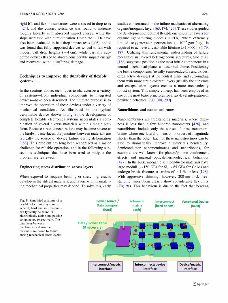
rigid ICs and flexible substrates were assessed in drop tests
[424], and the contact resistance was found to increase
roughly linearly with absorbed impact energy, while the
slope increased with humidification. Complete LCDs have
also been evaluated in ball drop impact tests [406], and it
was found that fully supported devices tended to fail with
modest ball drop heights (*4 cm), while partially sup-
ported devices flexed to absorb considerable impact energy
and recovered without suffering damage.
Techniques to improve the durability of flexiblesystems
In the sections above, techniques to characterize a variety
of systems—from individual components to integrated
devices—have been described. The ultimate purpose is to
improve the operation of these devices under a variety of
mechanical conditions. As illustrated in the typical
deformable device shown in Fig. 8, the development of
complete flexible electronics systems necessitates a com-
bination of several diverse materials within a single plat-
form. Because stress concentrations may become severe at
the hard/soft interfaces, the junctions between materials are
typically the source of device failure during deformation
[188]. This problem has long been recognized as a major
challenge for reliable operation, and in the following sub-
sections techniques that have been used to mitigate the
problem are reviewed.
Engineering stress distribution across layers
When exposed to frequent bending or stretching, cracks
develop in the stiffest materials, and layers with mismatch-
ing mechanical properties may debond. To solve this, early
studies concentrated on the failure mechanics of alternating
organic/inorganic layers [63, 174, 425]. These studies guided
the development of optimal flexible encapsulation layers for
organic light-emitting diodes (OLEDs), where extremely
limited oxygen/water permeation (*10-6 g/m2/day) is
required to achieve a reasonable lifetime ([10,000 h) [179,
187]. Utilizing this fundamental understanding of failure
mechanics in layered heterogeneous structures, Suo et al.
[168] suggested positioning the most brittle components in a
neutral mechanical plane, as described above. Positioning
the brittle components (usually semiconductors and oxides;
often active devices) at the neutral plane and surrounding
them with more strain-tolerant layers (usually the substrate
and encapsulation layers) creates a more mechanically
robust system. This simple concept has been employed as
one of the most basic principles for array-level integration of
flexible electronics [200, 288, 299].
Nanoribbons and nanomembranes
Nanomembranes are freestanding materials, where thick-
ness is less than a few hundred nanometers [426], and
nanoribbons include only the subset of these nanomem-
branes where one lateral dimension is orders of magnitude
shorter than the other. Each of these nanostructures can be
used to dramatically improve a material’s bendability.
Semiconductor nanomembranes and nanoribbons, for
example, are well known for photon/phonon confinement
effects and unusual optical/thermoelectrical behaviour
[427]. In the bulk, inorganic semiconductor materials have
large moduli (*150 GPa for Si, *85 GPa for GaAs) and
undergo brittle fracture at strains of *1 % or less [198].
With aggressive thinning, however, 200-nm-thick free-
standing nanoribbons clearly show considerable flexibility
(Fig. 9a). This behaviour is due to the fact that bending
Func�onal Device(hard)
Interconnect(hard or so�)
Power source /Data transport
(hard)
Data / Power Cable(if necessary)
Polymeric matrix(so�)
Interconnect/matrixinterface
Interconnect/deviceinterface
Device/matrixinterface
Fig. 8 Simplified anatomy of a
flexible electronics system. In
general, hard and soft materials
can typically be found in
electronically active and passive
components, respectively. The
interfaces between
mechanically dissimilar
materials are prone to failure
during mechanical stress cycles
J Mater Sci (2016) 51:2771–2805 2791
123
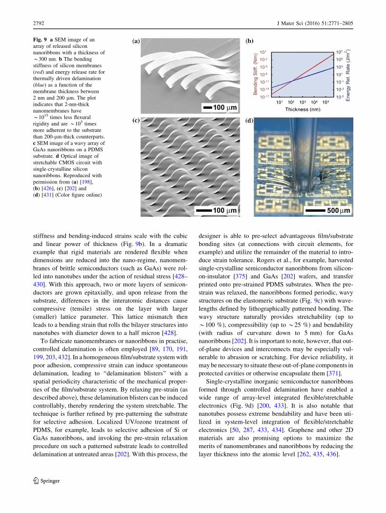
stiffness and bending-induced strains scale with the cubic
and linear power of thickness (Fig. 9b). In a dramatic
example that rigid materials are rendered flexible when
dimensions are reduced into the nano-regime, nanomem-
branes of brittle semiconductors (such as GaAs) were rol-
led into nanotubes under the action of residual stress [428–
430]. With this approach, two or more layers of semicon-
ductors are grown epitaxially, and upon release from the
substrate, differences in the interatomic distances cause
compressive (tensile) stress on the layer with larger
(smaller) lattice parameter. This lattice mismatch then
leads to a bending strain that rolls the bilayer structures into
nanotubes with diameter down to a half micron [428].
To fabricate nanomembranes or nanoribbons in practise,
controlled delamination is often employed [89, 170, 191,
199, 203, 432]. In a homogeneous film/substrate systemwith
poor adhesion, compressive strain can induce spontaneous
delamination, leading to ‘‘delamination blisters’’ with a
spatial periodicity characteristic of the mechanical proper-
ties of the film/substrate system. By relaxing pre-strain (as
described above), these delamination blisters can be induced
controllably, thereby rendering the system stretchable. The
technique is further refined by pre-patterning the substrate
for selective adhesion. Localized UV/ozone treatment of
PDMS, for example, leads to selective adhesion of Si or
GaAs nanoribbons, and invoking the pre-strain relaxation
procedure on such a patterned substrate leads to controlled
delamination at untreated areas [202]. With this process, the
designer is able to pre-select advantageous film/substrate
bonding sites (at connections with circuit elements, for
example) and utilize the remainder of the material to intro-
duce strain tolerance. Rogers et al., for example, harvested
single-crystalline semiconductor nanoribbons from silicon-
on-insulator [375] and GaAs [202] wafers, and transfer
printed onto pre-strained PDMS substrates. When the pre-
strain was relaxed, the nanoribbons formed periodic, wavy
structures on the elastomeric substrate (Fig. 9c) with wave-
lengths defined by lithographically patterned bonding. The
wavy structure naturally provides stretchability (up to
*100 %), compressibility (up to *25 %) and bendability
(with radius of curvature down to 5 mm) for GaAs
nanoribbons [202]. It is important to note, however, that out-
of-plane devices and interconnects may be especially vul-
nerable to abrasion or scratching. For device reliability, it
may be necessary to situate these out-of-plane components in
protected cavities or otherwise encapsulate them [371].
Single-crystalline inorganic semiconductor nanoribbons
formed through controlled delamination have enabled a
wide range of array-level integrated flexible/stretchable
electronics (Fig. 9d) [200, 433]. It is also notable that
nanotubes possess extreme bendability and have been uti-
lized in system-level integration of flexible/stretchable
electronics [50, 287, 433, 434]. Graphene and other 2D
materials are also promising options to maximize the
merits of nanomembranes and nanoribbons by reducing the
layer thickness into the atomic level [262, 435, 436].
Fig. 9 a SEM image of an
array of released silicon
nanoribbons with a thickness of
*300 nm. b The bending
stiffness of silicon membranes
(red) and energy release rate for
thermally driven delamination
(blue) as a function of the
membrane thickness between
2 nm and 200 lm. The plot
indicates that 2-nm-thick
nanomembranes have
*1015 times less flexural
rigidity and are *105 times
more adherent to the substrate
than 200-lm-thick counterparts.
c SEM image of a wavy array of
GaAs nanoribbons on a PDMS
substrate. d Optical image of
stretchable CMOS circuit with
single-crystalline silicon
nanoribbons. Reproduced with
permission from (a) [198],(b) [426], (c) [202] and(d) [431] (Color figure online)
2792 J Mater Sci (2016) 51:2771–2805
123
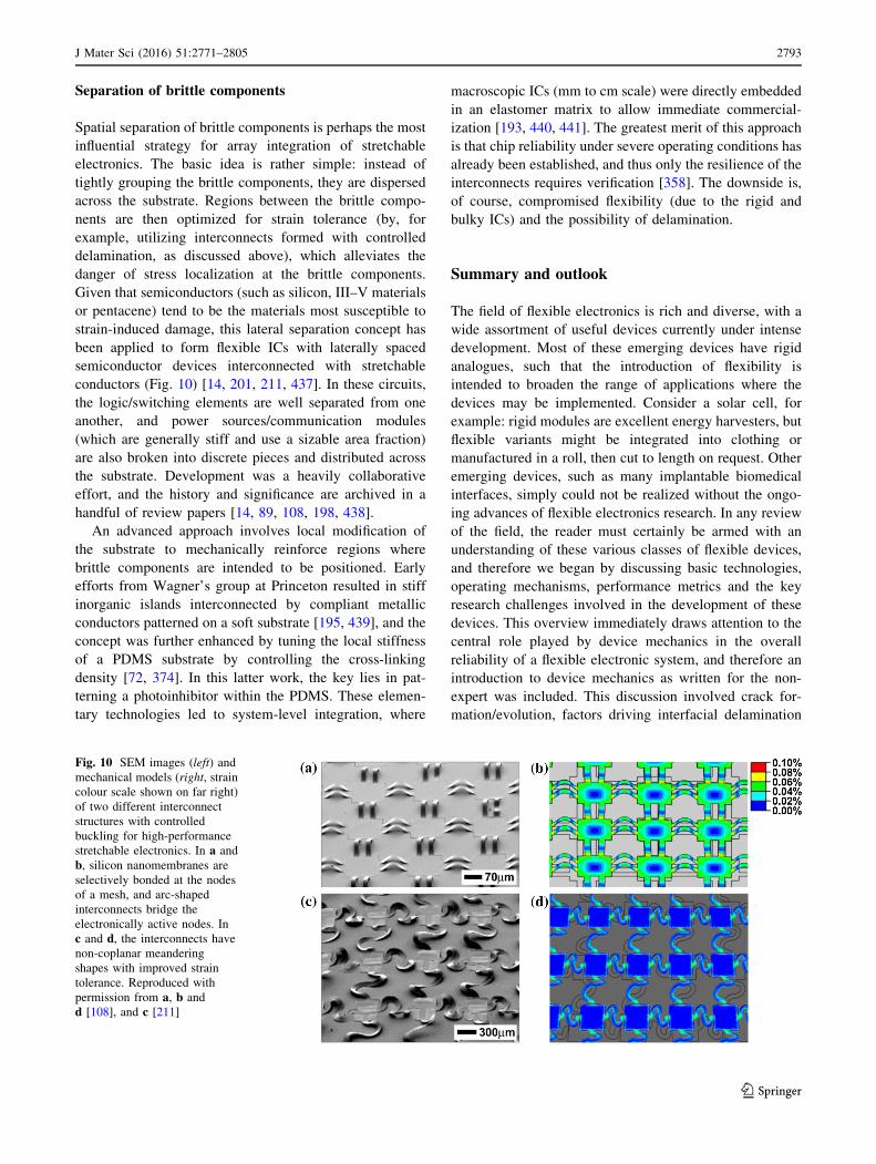
Separation of brittle components
Spatial separation of brittle components is perhaps the most
influential strategy for array integration of stretchable
electronics. The basic idea is rather simple: instead of
tightly grouping the brittle components, they are dispersed
across the substrate. Regions between the brittle compo-
nents are then optimized for strain tolerance (by, for
example, utilizing interconnects formed with controlled
delamination, as discussed above), which alleviates the
danger of stress localization at the brittle components.
Given that semiconductors (such as silicon, III–V materials
or pentacene) tend to be the materials most susceptible to
strain-induced damage, this lateral separation concept has
been applied to form flexible ICs with laterally spaced
semiconductor devices interconnected with stretchable
conductors (Fig. 10) [14, 201, 211, 437]. In these circuits,
the logic/switching elements are well separated from one
another, and power sources/communication modules
(which are generally stiff and use a sizable area fraction)
are also broken into discrete pieces and distributed across
the substrate. Development was a heavily collaborative
effort, and the history and significance are archived in a
handful of review papers [14, 89, 108, 198, 438].
An advanced approach involves local modification of
the substrate to mechanically reinforce regions where
brittle components are intended to be positioned. Early
efforts from Wagner’s group at Princeton resulted in stiff
inorganic islands interconnected by compliant metallic
conductors patterned on a soft substrate [195, 439], and the
concept was further enhanced by tuning the local stiffness
of a PDMS substrate by controlling the cross-linking
density [72, 374]. In this latter work, the key lies in pat-
terning a photoinhibitor within the PDMS. These elemen-
tary technologies led to system-level integration, where
macroscopic ICs (mm to cm scale) were directly embedded
in an elastomer matrix to allow immediate commercial-
ization [193, 440, 441]. The greatest merit of this approach
is that chip reliability under severe operating conditions has
already been established, and thus only the resilience of the
interconnects requires verification [358]. The downside is,
of course, compromised flexibility (due to the rigid and
bulky ICs) and the possibility of delamination.
Summary and outlook
The field of flexible electronics is rich and diverse, with a
wide assortment of useful devices currently under intense
development. Most of these emerging devices have rigid
analogues, such that the introduction of flexibility is
intended to broaden the range of applications where the
devices may be implemented. Consider a solar cell, for
example: rigid modules are excellent energy harvesters, but
flexible variants might be integrated into clothing or
manufactured in a roll, then cut to length on request. Other
emerging devices, such as many implantable biomedical
interfaces, simply could not be realized without the ongo-
ing advances of flexible electronics research. In any review
of the field, the reader must certainly be armed with an
understanding of these various classes of flexible devices,
and therefore we began by discussing basic technologies,
operating mechanisms, performance metrics and the key
research challenges involved in the development of these
devices. This overview immediately draws attention to the
central role played by device mechanics in the overall
reliability of a flexible electronic system, and therefore an
introduction to device mechanics as written for the non-
expert was included. This discussion involved crack for-
mation/evolution, factors driving interfacial delamination
Fig. 10 SEM images (left) and
mechanical models (right, strain
colour scale shown on far right)
of two different interconnect
structures with controlled
buckling for high-performance
stretchable electronics. In a and
b, silicon nanomembranes are
selectively bonded at the nodes
of a mesh, and arc-shaped
interconnects bridge the
electronically active nodes. In
c and d, the interconnects have
non-coplanar meandering
shapes with improved strain
tolerance. Reproduced with
permission from a, b and
d [108], and c [211]
J Mater Sci (2016) 51:2771–2805 2793
123
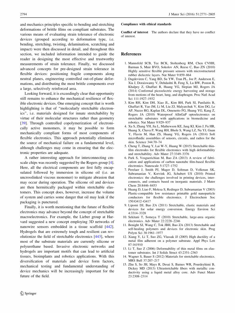
and mechanics principles specific to bending and stretching
deformations of brittle films on compliant substrates. The
various means of evaluating strain tolerance of electronic
devices (grouped according to deformation type, i.e.
bending, stretching, twisting, delamination, scratching and
impact) were then discussed in detail, and throughout this
section, we included information intended to guide the
reader in designing the most effective and trustworthy
measurements of strain tolerance. Finally, we discussed
advanced concepts for pre-designed strain tolerance in
flexible devices: positioning fragile components along
neutral planes, engineering controlled out-of-plane defor-
mations, and distributing the most brittle components over
a large, selectively reinforced area.
Looking forward, it is exceedingly clear that opportunity
still remains to enhance the mechanical resilience of flex-
ible electronic devices. One emerging concept that is worth
highlighting is that of ‘‘molecularly stretchable electron-
ics’’, i.e. materials designed for innate stretchability by
virtue of their molecular structures rather than geometry
[39]. Through controlled copolymerization of electroni-
cally active monomers, it may be possible to form
mechanically compliant forms of most components of
flexible electronics. This approach potentially eliminates
the source of mechanical failure on a fundamental level,
although challenges may come in ensuring that the elec-
tronic properties are adequate.
A rather interesting approach for interconnecting cm-
scale chips was recently suggested by the Rogers group [4].
Here, all the electrical components are first fully encap-
sulated followed by immersion in silicone oil (i.e. an
uncrosslinked viscous monomer) to mitigate abrasion that
may occur during operation. The silicone oil and devices
are then hermitically packaged within stretchable elas-
tomers. This concept does, however, increase the volume
of system and carries some danger that oil may leak if the
packaging is punctured.
Finally, it is worth mentioning that the future of flexible
electronics may advance beyond the concept of stretchable
macroelectronics. For example, the Lieber group at Har-
vard suggested a new concept employing 3D networks of
nanowire sensors embedded in a tissue scaffold [442].
Hydrogels that are extremely tough and resilient can rev-
olutionize the field of stretchable electronics [443], where
most of the substrate materials are currently silicone or
polyurethane based. Invasive electronic networks and
hydrogels are important motifs that can lead to artificial
tissues, bioimplants and robotics applications. With this
diversification of materials and device form factors,
mechanical testing and fundamental understanding of
device mechanics will be increasingly important for the
future of the field.
Compliance with ethical standards
Conflict of interest The authors declare that they have no conflict
of interest.
References
1. Mannsfeld SCB, Tee BCK, Stoltenberg RM, Chen CVHH,
Barman S, Muir BVO, Sokolov AN, Reese C, Bao ZN (2010)
Highly sensitive flexible pressure sensors with microstructured
rubber dielectric layers. Nat Mater 9:859–864
2. Dagdeviren C, Yang BD, Su YW, Tran PL, Joe P, Anderson E,
Xia J, Doraiswamy V, Dehdashti B, Feng X, Lu BW, Poston R,
Khalpey Z, Ghaffari R, Huang YG, Slepian MJ, Rogers JA
(2014) Conformal piezoelectric energy harvesting and storage
from motions of the heart, lung, and diaphragm. Proc Natl Acad
Sci 111:1927–1932
3. Kim RH, Kim DH, Xiao JL, Kim BH, Park SI, Panilaitis B,
Ghaffari R, Yao JM, Li M, Liu ZJ, Malyarchuk V, Kim DG, Le
AP, Nuzzo RG, Kaplan DL, Omenetto FG, Huang YG, Kang Z,
Rogers JA (2010) Waterproof AlInGaP optoelectronics on
stretchable substrates with applications in biomedicine and
robotics. Nat Mater 9:929–937
4. Xu S, Zhang YH, Jia L, Mathewson KE, Jang KI, Kim J, Fu HR,
Huang X, Chava P, Wang RH, Bhole S, Wang LZ, Na YJ, Guan
Y, Flavin M, Han ZS, Huang YG, Rogers JA (2014) Soft
microfluidic assemblies of sensors, circuits, and radios for the
skin. Science 344:70–74
5. Cheng T, Zhang Y, Lai W-Y, Huang W (2015) Stretchable thin-
film electrodes for flexible electronics with high deformability
and stretchability. Adv Mater 27:3349–3376
6. Park S, Vosguerichian M, Bao ZA (2013) A review of fabri-
cation and applications of carbon nanotube film-based flexible
electronics. Nanoscale 5:1727–1752
7. Perelaer J, Smith PJ, Mager D, Soltman D, Volkman SK,
Subramanian V, Korvink JG, Schubert US (2010) Printed
electronics: the challenges involved in printing devices, inter-
connects, and contacts based on inorganic materials. J Mater
Chem 20:8446–8453
8. Huang D, Liao F, Molesa S, Redinger D, Subramanian V (2003)
Plastic-compatible low resistance printable gold nanoparticle
conductors for flexible electronics. J Electrochem Soc
150:G412–G417
9. Lipomi DJ, Bao ZA (2011) Stretchable, elastic materials and
devices for solar energy conversion. Energy Environ Sci
4:3314–3328
10. Sekitani T, Someya T (2010) Stretchable, large-area organic
electronics. Adv Mater 22:2228–2246
11. Benight SJ, Wang C, Tok JBH, Bao ZA (2013) Stretchable and
self-healing polymers and devices for electronic skin. Prog
Polym Sci 38:1961–1977
12. Xiang Y, Li T, Suo ZG, Vlassak JJ (2005) High ductility of a
metal film adherent on a polymer substrate. Appl Phys Lett
87:161910
13. Li T, Suo Z (2006) Deformability of thin metal films on elas-
tomer substrates. Int J Solids Struct 43:2351–2363
14. Wagner S, Bauer S (2012) Materials for stretchable electronics.
MRS Bull 37:207–217
15. Zhu S, So JH, Mays R, Desai S, Barnes WR, Pourdeyhimi B,
Dickey MD (2013) Ultrastretchable fibers with metallic con-
ductivity using a liquid metal alloy core. Adv Funct Mater
23:2308–2314
2794 J Mater Sci (2016) 51:2771–2805
123
16. Park J, Wang SD, Li M, Ahn C, Hyun JK, Kim DS, Kim DK,
Rogers JA, Huang YG, Jeon S (2012) Three-dimensional
nanonetworks for giant stretchability in dielectrics and con-
ductors. Nat Commun 3:916
17. Cheng S, Wu ZG (2011) A microfluidic, reversibly stretchable,
large-area wireless strain sensor. Adv Funct Mater
21:2282–2290
18. Kubo M, Li XF, Kim C, Hashimoto M, Wiley BJ, Ham D,
Whitesides GM (2010) Stretchable microfluidic radiofrequency
antennas. Adv Mater 22:2749–2752
19. Cheng S, Wu ZG (2012) Microfluidic electronics. Lab Chip
12:2782–2791
20. Baca AJ, Ahn JH, Sun YG, Meitl MA, Menard E, Kim HS, Choi
WM, Kim DH, Huang Y, Rogers JA (2008) Semiconductor
wires and ribbons for high-performance flexible electronics.
Angew Chem Int Ed 47:5524–5542
21. Long YZ, Yu M, Sun B, Gu CZ, Fan ZY (2012) Recent
advances in large-scale assembly of semiconducting inorganic
nanowires and nanofibers for electronics, sensors and photo-
voltaics. Chem Soc Rev 41:4560–4580
22. Liu X, Long YZ, Liao L, Duan XF, Fan ZY (2012) Large-scale
integration of semiconductor nanowires for high-performance
flexible electronics. ACS Nano 6:1888–1900
23. Wu JH, Zang JF, Rathmell AR, Zhao XH, Wiley BJ (2013)
Reversible sliding in networks of nanowires. Nano Lett
13:2381–2386
24. Sun DM, Liu C, Ren WC, Cheng HM (2013) A review of carbon
nanotube- and graphene-based flexible thin-film transistors.
Small 9:1188–1205
25. Hecht DS, Hu LB, Irvin G (2011) Emerging transparent elec-
trodes based on thin films of carbon nanotubes, graphene, and
metallic nanostructures. Adv Mater 23:1482–1513
26. Hu LB, Kim HS, Lee JY, Peumans P, Cui Y (2010) Scalable
coating and properties of transparent, flexible, silver nanowire
electrodes. ACS Nano 4:2955–2963
27. Lee JY, Connor ST, Cui Y, Peumans P (2008) Solution-pro-
cessed metal nanowire mesh transparent electrodes. Nano Lett
8:689–692
28. Rathmell AR, Bergin SM, Hua YL, Li ZY, Wiley BJ (2010) The
growth mechanism of copper nanowires and their properties in
flexible, transparent conducting films. Adv Mater 22:3558–3563
29. Yao SS, Zhu Y (2015) Nanomaterial-enabled stretchable con-
ductors: strategies, materials and devices. Adv Mater
27:1480–1511
30. Huang JC (2002) Carbon black filled conducting polymers and
polymer blends. Adv Polym Technol 21:299–313
31. Strumpler R, Glatz-Reichenbach J (1999) Conducting polymer
composites. J Electroceram 3:329–346
32. Zhang W, Dehghani-Sanij AA, Blackburn RS (2007) Carbon
based conductive polymer composites. J Mater Sci
42:3408–3418. doi:10.1007/s10853-007-1688-5
33. Nyholm L, Nystrom G, Mihranyan A, Stromme M (2011)
Toward flexible polymer and paper-based energy storage devi-
ces. Adv Mater 23:3751–3769
34. Snook GA, Kao P, Best AS (2011) Conducting-polymer-based
supercapacitor devices and electrodes. J Power Sources
196:1–12
35. Bhadra S, Khastgir D, Singha NK, Lee JH (2009) Progress in
preparation, processing and applications of polyaniline. Prog
Polym Sci 34:783–810
36. Halpin JC (1969) Stiffness and expansion estimates for oriented
short fiber composites. J Compos Mater 3:732–734
37. Rafiee MA, Rafiee J, Wang Z, Song HH, Yu ZZ, Koratkar N
(2009) Enhanced mechanical properties of nanocomposites at
low graphene content. ACS Nano 3:3884–3890
38. Horowitz G (2006) Organic transistors. In: Klauk H (ed)
Organic electronics, materials, manufacturing and applications.
Wiley-VCH, Weinheim, pp 3–32
39. Savagatrup S, Printz AD, O’Connor TF, Zaretski AV, Lipomi
DJ (2014) Molecularly stretchable electronics. Chem Mater
26:3028–3041
40. Heeger AJ (2001) Nobel lecture: semiconducting and metallic
polymers: the fourth generation of polymeric materials. Rev
Mod Phys 73:681–700
41. Elschner A, Kirchmeyer S, Lovenich W, Merker U, Reuter K
(2011) PEDOT: principles and applications of an intrinsically
conductive polymer. CRC Press, New York
42. Weiss NO, Zhou HL, Liao L, Liu Y, Jiang S, Huang Y, Duan XF
(2012) Graphene: an emerging electronic material. Adv Mater
24:5782–5825
43. Lee C, Wei XD, Kysar JW, Hone J (2008) Measurement of the
elastic properties and intrinsic strength of monolayer graphene.
Science 321:385–388
44. Kang J, Shin D, Bae S, Hong BH (2012) Graphene transfer: key
for applications. Nanoscale 4:5527–5537
45. Torrisi F, Hasan T, Wu WP, Sun ZP, Lombardo A, Kulmala TS,
Hsieh GW, Jung SJ, Bonaccorso F, Paul PJ, Chu DP, Ferrari AC
(2012) Inkjet-printed graphene electronics. ACS Nano
6:2992–3006
46. Sun YG, Rogers JA (2007) Inorganic semiconductors for flexi-
ble electronics. Adv Mater 19:1897–1916
47. Guillen C, Herrero J (2011) TCO/metal/TCO structures for
energy and flexible electronics. Thin Solid Films 520:1–17
48. Hecht DS, Kaner RB (2011) Solution-processed transparent
electrodes. MRS Bull 36:749–755
49. Layani M, Kamyshny A, Magdassi S (2014) Transparent con-
ductors composed of nanomaterials. Nanoscale 6:5581–5591
50. Lu W, Lieber CM (2006) Semiconductor nanowires. J Phys D
Appl Phys 39:R387–R406
51. Katz HE, Huang J (2009) Thin-film organic electronic devices.
Annu Rev Mater Res 39:71–92
52. Wang XS, Tang HP, Li XD, Hua X (2009) Investigations on the
mechanical properties of conducting polymer coating-substrate
structures and their influencing factors. Int J Mol Sci
10:5257–5284
53. Biswas C, Lee YH (2011) Graphene versus carbon nanotubes in
electronic devices. Adv Funct Mater 21:3806–3826
54. Tahk D, Lee HH, Khang DY (2009) Elastic moduli of organic
electronic materials by the buckling method. Macromolecules
42:7079–7083
55. Savagatrup S, Makaram AS, Burke DJ, Lipomi DJ (2014)
Mechanical properties of conjugated polymers and polymer-
fullerene composites as a function of molecular structure. Adv
Funct Mater 24:1169–1181
56. O’Connor B, Chan EP, Chan C, Conrad BR, Richter LJ, Kline
RJ, Heeney M, McCulloch I, Soles CL, DeLongchamp DM
(2010) Correlations between mechanical and electrical proper-
ties of polythiophenes. ACS Nano 4:7538–7544
57. Awartani O, Lemanski BI, Ro HW, Richter LJ, DeLongchamp
DM, O’Connor BT (2013) Correlating stiffness, ductility, and
morphology of polymer:fullerene films for solar cell applica-
tions. Adv Energy Mater 3:399–406
58. Savagatrup S, Printz AD, Rodriquez D, Lipomi DJ (2014) Best
of both worlds: conjugated polymers exhibiting good photo-
voltaic behavior and high tensile elasticity. Macromolecules
47:1981–1992
59. Printz AD, Savagatrup S, Burke DJ, Purdy TN, Lipomi DJ
(2014) Increased elasticity of a low-bandgap conjugated
copolymer by random segmentation for mechanically robust
solar cells. RSC Adv 4:13635–13643
J Mater Sci (2016) 51:2771–2805 2795
123
60. Green MA, Ho-Baillie A, Snaith HJ (2014) The emergence of
perovskite solar cells. Nat Photonics 8:506–514
61. Snaith HJ (2013) Perovskites: the emergence of a new era for
low-cost, high-efficiency solar cells. J Phys Chem Lett
4:3623–3630
62. Cao Q, Xia MG, Shim M, Rogers JA (2006) Bilayer organic-
inorganic gate dielectrics for high-performance, low-voltage,
single-walled carbon nanotube thin-film transistors, comple-
mentary logic gates, and p-n diodes on plastic substrates. Adv
Funct Mater 16:2355–2362
63. Leterrier Y (2003) Durability of nanosized oxygen-barrier
coatings on polymers—internal stresses. Prog Mater Sci 48:1–55
64. Zardetto V, Brown TM, Reale A, Di Carlo A (2011) Substrates
for flexible electronics: a practical investigation on the electri-
cal, film flexibility, optical, temperature, and solvent resistance
properties. J Polym Sci B Polym Phys 49:638–648
65. Fortunato G, Pecora A, Maiolo L (2012) Polysilicon thin-film
transistors on polymer substrates. Mater Sci Semicond Process
15:627–641
66. Nathan A, Ahnood A, Cole MT, Lee S, Suzuki Y, Hiralal P,
Bonaccorso F, Hasan T, Garcia-Gancedo L, Dyadyusha A,
Haque S, Andrew P, Hofmann S, Moultrie J, Chu DP, Flewitt
AJ, Ferrari AC, Kelly MJ, Robertson J, Amaratunga GAJ, Milne
WI (2012) Flexible electronics: the next ubiquitous platform.
Proc IEEE 100:1486–1517
67. Xu Y (2013) Post-CMOS and post-MEMS compatible flexible
skin technologies: a review. IEEE Sens J 13:3962–3975
68. Toivola M, Halme J, Miettunen K, Aitola K, Lund PD (2009)
Nanostructured dye solar cells on flexible substrates. Int J
Energy Res 33:1145–1160
69. MacDonald WA, Looney MK, MacKerron D, Eveson R, Rakos
K (2008) Designing and manufacturing substrates for flexible
electronics. Plast Rubber Compos 37:41–45
70. MacDonald WA, Looney MK, MacKerron D, Eveson R, Adam
R, Hashimoto K, Rakos K (2007) Latest advances in substrates
for flexible electronics. J Soc Inf Disp 15:1075–1083
71. Vijay V, Rao AD, Narayan KS (2011) In situ studies of strain
dependent transport properties of conducting polymers on
elastomeric substrates. J Appl Phys 109:084525
72. Cotton DPJ, Popel A, Graz IM, Lacour SP (2011) Photopat-
terning the mechanical properties of polydimethylsiloxane films.
J Appl Phys 109:054905
73. Takahashi T, Takei K, Gillies AG, Fearing RS, Javey A (2011)
Carbon nanotube active-matrix backplanes for conformal elec-
tronics and sensors. Nano Lett 11:5408–5413
74. Tobjork D, Osterbacka R (2011) Paper electronics. Adv Mater
23:1935–1961
75. Hu LB, Cui Y (2012) Energy and environmental nanotechnol-
ogy in conductive paper and textiles. Energy Environ Sci
5:6423–6435
76. Lukowicz P, Kirstein T, Troster G (2004) Wearable systems for
health care applications. Methods Inf Med 43:232–238
77. Park S, Jayaraman S (2003) Smart textiles: wearable electronic
systems. MRS Bull 28:585–591
78. Salvado R, Loss C, Goncalves R, Pinho P (2012) Textile
materials for the design of wearable antennas: a survey. Sensors
12:15841–15857
79. Axisa F, Schmitt PM, Gehin C, Delhomme G, McAdams E,
Dittmar A (2005) Flexible technologies and smart clothing for
citizen medicine, home healthcare, and disease prevention. IEEE
Trans Inf Technol Biomed 9:325–336
80. Zeng W, Shu L, Li Q, Chen S, Wang F, Tao XM (2014) Fiber-
based wearable electronics: a review of materials, fabrication,
devices, and applications. Adv Mater 26:5310–5336
81. Hu LB, Pasta M, La Mantia F, Cui LF, Jeong S, Deshazer HD,
Choi JW, Han SM, Cui Y (2010) Stretchable, porous, and
conductive energy textiles. Nano Lett 10:708–714
82. Sazonov A, Meitine M, Stryakhilev D, Nathan A (2006) Low-
temperature materials and thin-film transistors for electronics on
flexible substrates. Semiconductors 40:959–967
83. Zhang K, Seo JH, Zhou WD, Ma ZQ (2012) Fast flexible
electronics using transferrable silicon nanomembranes. J Phys D
Appl Phys 45:143001
84. Cho JH, Lee J, Xia Y, Kim B, He YY, Renn MJ, Lodge TP,
Frisbie CD (2008) Printable ion-gel gate dielectrics for low-
voltage polymer thin-film transistors on plastic. Nat Mater
7:900–906
85. Zaumseil J, Sirringhaus H (2007) Electron and ambipolar
transport in organic field-effect transistors. Chem Rev
107:1296–1323
86. Chung HJ, Kim TI, Kim HS, Wells SA, Jo S, Ahmed N, Jung
YH, Won SM, Bower CA, Rogers JA (2011) Fabrication of
releasable single-crystal silicon-metal oxide field-effect devices
and their deterministic assembly on foreign substrates. Adv
Funct Mater 21:3029–3036
87. Kim TI, Jung YH, Chung HJ, Yu KJ, Ahmed N, Corcoran CJ,
Park JS, Jin SH, Rogers JA (2013) Deterministic assembly of
releasable single crystal silicon-metal oxide field-effect devices
formed from bulk wafers. Appl Phys Lett 102:182104
88. Han ST, Zhou Y, Roy VAL (2013) Towards the development of
flexible non-volatile memories. Adv Mater 25:5425–5449
89. Kim DH, Xiao JL, Song JZ, Huang YG, Rogers JA (2010)
Stretchable, curvilinear electronics based on inorganic materials.
Adv Mater 22:2108–2124
90. Kim TI, Kim RH, Rogers JA (2012) Microscale inorganic light-
emitting diodes on flexible and stretchable substrates. IEEE
Photon J 4:607–612
91. Tok JBH, Bao ZA (2012) Recent advances in flexible and
stretchable electronics, sensors and power sources. Sci China
Chem 55:718–725
92. Weerasinghe HC, Huang FZ, Cheng YB (2013) Fabrication of
flexible dye sensitized solar cells on plastic substrates. Nano
Energy 2:174–189
93. Dennler G, Sariciftci NS (2005) Flexible conjugated polymer-
based plastic solar cells: from basics to applications. Proc IEEE
93:1429–1439
94. Angmo D, Krebs FC (2013) Flexible ITO-free polymer solar
cells. J Appl Polym Sci 129:1–14
95. Xie KY, Wei BQ (2014) Materials and structures for stretchable
energy storage and conversion devices. Adv Mater
26:3592–3617
96. Goetzberger A, Hebling C, Schock HW (2003) Photovoltaic
materials, history, status and outlook. Mater Sci Eng, R 40:1–46
97. Lee SY, Choi KH, Choi WS, Kwon YH, Jung HR, Shin HC,
Kim JY (2013) Progress in flexible energy storage and conver-
sion systems, with a focus on cable-type lithium-ion batteries.
Energy Environ Sci 6:2414–2423
98. Gwon H, Hong J, Kim H, Seo DH, Jeon S, Kang K (2014)
Recent progress on flexible lithium rechargeable batteries.
Energy Environ Sci 7:538–551
99. Zhou GM, Li F, Cheng HM (2014) Progress in flexible lithium
batteries and future prospects. Energy Environ Sci 7:1307–1338
100. Zhang Y, Huang Y, Rogers JA (2015) Mechanics of stretchable
batteries and supercapacitors. Curr Opin Solid State Mater Sci
19:190–199
101. Bates JB, Dudney NJ, Neudecker B, Ueda A, Evans CD (2000)
Thin-film lithium and lithium-ion batteries. Solid State Ionics
135:33–45
2796 J Mater Sci (2016) 51:2771–2805
123
102. Xu S, Zhang YH, Cho J, Lee J, Huang X, Jia L, Fan JA, Su YW,
Su J, Zhang HG, Cheng HY, Lu BW, Yu CJ, Chuang C, Kim TI,
Song T, Shigeta K, Kang S, Dagdeviren C, Petrov I, Braun PV,
Huang YG, Paik U, Rogers JA (2013) Stretchable batteries with
self-similar serpentine interconnects and integrated wireless
recharging systems. Nat Commun 4:1543
103. Koo JH, Seo J, Lee T (2012) Nanomaterials on flexible sub-
strates to explore innovative functions: from energy harvesting
to bio-integrated electronics. Thin Solid Films 524:1–19
104. Chen Y, Lu BW, Ou DP, Feng X (2015) Mechanics of flexible
and stretchable piezoelectrics for energy harvesting. Sci China
Phys Mech Astron 58:594601
105. Roberts ME, Sokolov AN, Bao ZN (2009) Material and device
considerations for organic thin-film transistor sensors. J Mater
Chem 19:3351–3363
106. Hammock ML, Chortos A, Tee BCK, Tok JBH, Bao ZA (2013)
The evolution of electronic skin (e-skin): a brief history, design
considerations, and recent progress. Adv Mater 25:5997–6037
107. Kim DH, Ghaffari R, Lu NS, Rogers JA (2012) Flexible and
stretchable electronics for biointegrated devices. Annu Rev
Biomed Eng 14:113–128
108. Kim DH, Lu NS, Huang YG, Rogers JA (2012) Materials for
stretchable electronics in bioinspired and biointegrated devices.
MRS Bull 37:226–235
109. Minev IR, Musienko P, Hirsch A, Barraud Q, Wenger N,
Moraud EM, Gandar J, Capogrosso M, Milekovic T, Asboth L,
Torres RF, Vachicouras N, Liu Q, Pavlova N, Duis S, Lar-
magnac A, Voros J, Micera S, Suo Z, Courtine G, Lacour SP
(2015) Electronic dura mater for long-term multimodal neural
interfaces. Science 347:159–163
110. Rivnay J, Owens RM, Malliaras GG (2014) The rise of organic
bioelectronics. Chem Mater 26:679–685
111. Jeong J-W, Shin G, Park SI, Yu KJ, Xu L, Rogers JA (2015)
Soft materials in neuroengineering for hard problems in neuro-
science. Neuron 86:175–186
112. Kim DH, Lu NS, Ma R, Kim YS, Kim RH, Wang SD, Wu J,
Won SM, Tao H, Islam A, Yu KJ, Kim TI, Chowdhury R, Ying
M, Xu LZ, Li M, Chung HJ, Keum H, McCormick M, Liu P,
Zhang YW, Omenetto FG, Huang YG, Coleman T, Rogers JA
(2011) Epidermal electronics. Science 333:838–843
113. Yeo WH, Kim YS, Lee J, Ameen A, Shi LK, Li M, Wang SD,
Ma R, Jin SH, Kang Z, Huang YG, Rogers JA (2013) Multi-
functional epidermal electronics printed directly onto the skin.
Adv Mater 25:2773–2778
114. Jang KI, Han SY, Xu S, Mathewson KE, Zhang YH, Jeong JW,
Kim GT, Webb C, Lee JW, Dawidczyk TJ, Kim RH, Song YM,
Yeo WH, Kim S, Cheng HY, Il Rhee S, Chung J, Kim B, Chung
HU, Lee DJ, Yang YY, Cho M, Gaspar JG, Carbonari R, Fabiani
M, Gratton G, Huang YG, Rogers JA (2014) Rugged and
breathable forms of stretchable electronics with adherent com-
posite substrates for transcutaneous monitoring. Nat Commun
5:4779
115. Huang X, Liu YH, Cheng HY, Shin WJ, Fan JA, Liu ZJ, Lu CJ,
Kong GW, Chen K, Patnaik D, Lee SH, Hage-Ali S, Huang YG,
Rogers JA (2014) Materials and designs for wireless epidermal
sensors of hydration and strain. Adv Funct Mater 24:3846–3854
116. Bandodkar AJ, Jia WZ, Wang J (2015) Tattoo-based wearable
electrochemical devices: a review. Electroanalysis 27:562–572
117. Bandodkar AJ, Hung VWS, Jia WZ, Valdes-Ramirez G,
Windmiller JR, Martinez AG, Ramirez J, Chan G, Kerman K,
Wang J (2013) Tattoo-based potentiometric ion-selective sen-
sors for epidermal pH monitoring. Analyst 138:123–128
118. Bandodkar AJ, Molinnus D, Mirza O, Guinovart T, Windmiller
JR, Valdes-Ramirez G, Andrade FJ, Schoning MJ, Wang J
(2014) Epidermal tattoo potentiometric sodium sensors with
wireless signal transduction for continuous non-invasive sweat
monitoring. Biosens Bioelectron 54:603–609
119. Kim J, de Araujo WR, Samek IA, Bandodkar AJ, Jia WZ,
Brunetti B, Paixao TRLC, Wang J (2015) Wearable temporary
tattoo sensor for real-time trace metal monitoring in human
sweat. Electrochem Commun 51:41–45
120. Windmiller JR, Bandodkar AJ, Valdes-Ramirez G, Parkho-
movsky S, Martinez AG, Wang J (2012) Electrochemical
sensing based on printable temporary transfer tattoos. Chem
Commun 48:6794–6796
121. Bandodkar AJ, Nunez-Flores R, Jia W, Wang J (2015) All-
printed stretchable electrochemical devices. Adv Mater
27:3060–3065
122. Lumelsky VJ, Shur MS, Wagner S (2001) Sensitive skin. IEEE
Sens J 1:41–51
123. Lipomi DJ, Vosgueritchian M, Tee BCK, Hellstrom SL, Lee JA,
Fox CH, Bao ZN (2011) Skin-like pressure and strain sensors
based on transparent elastic films of carbon nanotubes. Nat
Nanotechnol 6:788–792
124. Wagner S, Lacour SP, Jones J, Hsu PHI, Sturm JC, Li T, Suo ZG
(2004) Electronic skin: architecture and components. Physica E
25:326–334
125. Chortos A, Bao Z (2014) Skin-inspired electronic devices. Mater
Today 17:321–331
126. Kim J, Lee M, Shim HJ, Ghaffari R, Cho HR, Son D, Jung YH,
Soh M, Choi C, Jung S, Chu K, Jeon D, Lee S-T, Kim JH, Choi
SH, Hyeon T, Kim D-H (2014) Stretchable silicon nanoribbon
electronics for skin prostheses. Nat Commun 5:5747
127. Viventi J, Kim DH, Vigeland L, Frechette ES, Blanco JA, Kim
YS,AvrinAE,TiruvadiVR,HwangSW,VanleerAC,WulsinDF,
Davis K, Gelber CE, Palmer L, Van der Spiegel J, Wu J, Xiao JL,
Huang YG, Contreras D, Rogers JA, Litt B (2011) Flexible,
foldable, actively multiplexed, high-density electrode array for
mapping brain activity in vivo. Nat Neurosci 14:1599–1605
128. Khaled I, Elmallah S, Cheng C, Moussa WA, Mushahwar VK,
Elias AL (2013) A flexible base electrode array for intraspinal
microstimulation. IEEE Trans Biomed Eng 60:2904–2913
129. Zrenner E, Bartz-Schmidt KU, Benav H, Besch D, Bruckmann
A, Gabel VP, Gekeler F, Greppmaier U, Harscher A, Kibbel S,
Koch J, Kusnyerik A, Peters T, Stingl K, Sachs H, Stett A,
Szurman P, Wilhelm B, Wilke R (2011) Subretinal electronic
chips allow blind patients to read letters and combine them to
words. Proc R Soc B 278:1489–1497
130. Xu LZ, Gutbrod SR, Bonifas AP, Su YW, Sulkin MS, Lu NS,
Chung HJ, Jang KI, Liu ZJ, Ying M, Lu C, Webb RC, Kim JS,
Laughner JI, Cheng HY, Liu YH, Ameen A, Jeong JW, Kim GT,
Huang YG, Efimov IR, Rogers JA (2014) 3D multifunctional
integumentary membranes for spatiotemporal cardiac measure-
ments and stimulation across the entire epicardium. Nat Com-
mun 5:3329
131. Potter-Baker KA, Capadona JR (2015) Reducing the ‘‘stress’’:
antioxidative therapeutic and material approaches may prevent
intracortical microelectrode failure. ACS Macro Lett 4:275–279
132. Holt DJ, Grainger DW (2012) Host response to biomaterials. In:
Hollinger JO (ed) An introduction to biomaterials. Taylor &
Francis Group, Boca Raton, FL, pp 91–118
133. Marin C, Fernandez E (2010) Biocompatibility of intracortical
microelectrodes: current status and future prospects. Front
Neuroeng 3:1–6
134. Prasad A, Sanchez JC (2012) Quantifying long-term micro-
electrode array functionality using chronic in vivo impedance
testing. J Neural Eng 9:026028
135. Biran R, Martin DC, Tresco PA (2005) Neuronal cell loss
accompanies the brain tissue response to chronically implanted
silicon microelectrode arrays. Exp Neurol 195:115–126
J Mater Sci (2016) 51:2771–2805 2797
123
136. Campbell SA (2001) The science and engineering of micro-
electronic fabrication. Oxford University Press, Oxford, UK
137. Alf ME, Asatekin A, Barr MC, Baxamusa SH, Chelawat H,
Ozaydin-Ince G, Petruczok CD, Sreenivasan R, Tenhaeff WE,
Trujillo NJ, Vaddiraju S, Xu JJ, Gleason KK (2010) Chemical
vapor deposition of conformal, functional, and responsive
polymer films. Adv Mater 22:1993–2027
138. Kim H, Lee HBR, Maeng WJ (2009) Applications of atomic
layer deposition to nanofabrication and emerging nanodevices.
Thin Solid Films 517:2563–2580
139. Knez M, Niesch K, Niinisto L (2007) Synthesis and surface
engineering of complex nanostructures by atomic layer deposi-
tion. Adv Mater 19:3425–3438
140. Moonen PF, Yakimets I, Huskens J (2012) Fabrication of tran-
sistors on flexible substrates: from mass-printing to high-reso-
lution alternative lithography strategies. Adv Mater 24:5526–
5541
141. Krebs FC (2009) Polymer solar cell modules prepared using
roll-to-roll methods: knife-over-edge coating, slot-die coating
and screen printing. Sol Energy Mater Sol Cells 93:465–475
142. Krebs FC, Gevorgyan SA, Alstrup J (2009) A roll-to-roll process
to flexible polymer solar cells: model studies, manufacture and
operational stability studies. J Mater Chem 19:5442–5451
143. Jain K, Klosner M, Zemel M, Raghunandan S (2005) Flexible
electronics and displays: high-resolution, roll-to-roll, projection
lithography and photoablation processing technologies for high-
throughput production. Proc IEEE 93:1500–1510
144. Treutlein R, Bergsmann M, Stonley CJ (2006) Reel-to-reel
vacuum metallization. In: Klauk H (ed) Organic electronics,
materials, manufacturing and applications. Wiley-VCH, Wein-
heim, pp 183–202
145. Reinhold E, Faber J (2011) Large area electron beam physical
vapor deposition (EB-PVD) and plasma activated electron beam
(EB) evaporation—Status and prospects. Surf Coat Technol
206:1653–1659
146. Ludwig R, Kukla R, Josephson E (2005) Vacuum web coating—
state of the art and potential for electronics. Proc IEEE
93:1483–1490
147. Juang ZY, Wu CY, Lu AY, Su CY, Leou KC, Chen FR, Tsai CH
(2010) Graphene synthesis by chemical vapor deposition and
transfer by a roll-to-roll process. Carbon 48:3169–3174
148. Kukla R, Ludwig R, Meinel J (1996) Overview on modern vac-
uum web coating technology. Surf Coat Technol 86–7:753–761
149. Kessels WMM, Putkonen M (2011) Advanced process tech-
nologies: plasma, direct-write, atmospheric pressure, and roll-to-
roll ALD. MRS Bull 36:907–913
150. Yin ZP, Huang YA, Bu NB, Wang XM, Xiong YL (2010) Inkjet
printing for flexible electronics: materials, processes and
equipments. Chin Sci Bull 55:3383–3407
151. Street RA, Wong WS, Ready SE, Chabinyc IL, Arias AC, Limb
S, Salleo A, Lujan R (2006) Jet printing flexible displays. Mater
Today 9:32–37
152. Ahn BY, Duoss EB, Motala MJ, Guo XY, Park SI, Xiong YJ,
Yoon J, Nuzzo RG, Rogers JA, Lewis JA (2009) Omnidirec-
tional printing of flexible, stretchable, and spanning silver
microelectrodes. Science 323:1590–1593
153. Muth JT, Vogt DM, Truby RL, Menguc Y, Kolesky DB, Wood
RJ, Lewis JA (2014) Embedded 3D printing of strain sensors
within highly stretchable elastomers. Adv Mater 26:6307–6312
154. Kadekar V, Fang WY, Liou F (2004) Deposition technologies
for micromanufacturing: a review. J Manuf Sci Eng Trans
ASME 126:787–795
155. Arnold CB, Serra P, Pique A (2007) Laser direct-write tech-
niques for printing of complex materials. MRS Bull 32:23–31
156. Huang ZM, Zhang YZ, Kotaki M, Ramakrishna S (2003) A
review on polymer nanofibers by electrospinning and their
applications in nanocomposites. Compos Sci Technol 63:2223–
2253
157. Li D, Xia YN (2004) Electrospinning of nanofibers: reinventing
the wheel? Adv Mater 16:1151–1170
158. Chabinyc ML, Wong WS, Arias AC, Ready S, Lujan RA,
Daniel JH, Krusor B, Apte RB, Salleo A, Street RA (2005)
Printing methods and materials for large-area electronic devices.
Proc IEEE 93:1491–1499
159. Lee C, Kang H, Kim H, Shin K (2010) Noble logic for pre-
venting scratch on roll-to-roll printed layers in noncontacting
transportation. Jpn J Appl Phys 49:05EC07
160. Keum H, Carlson A, Ning HL, Mihi A, Eisenhaure JD, Braun
PV, Rogers JA, Kim S (2012) Silicon micro-masonry using
elastomeric stamps for three-dimensional microfabrication.
J Micromech Microeng 22:055018
161. Keum H, Chung HJ, Kim S (2013) Electrical contact at the
interface between silicon and transfer-printed gold films by
eutectic joining. ACS Appl Mater Interfaces 5:6061–6065
162. Callister WD (2007) Materials science and engineering: an
introduction. John Wiley & Sons, New York
163. Lee YY, Lee JH, Cho JY, Kim NR, Nam DH, Choi IS, Nam KT,
Joo YC (2013) Stretching-induced growth of PEDOT-rich cores:
a new mechanism for strain-dependent resistivity change in
PEDOT:PSS films. Adv Funct Mater 23:4020–4027
164. Herakovich CT (1981) On the relationship between engineering
properties and delamination of composite-materials. J Compos
Mater 15:336–348
165. Leterrier Y, Pellaton D, Mendels D, Glauser R, Andersons J,
Manson JAE (2001) Biaxial fragmentation of thin silicon oxide
coatings on poly(ethylene terephthalate). J Mater Sci
36:2213–2225. doi:10.1023/A:1017552302379
166. Gleskova H, Cheng IC, Wagner S, Sturm JC, Suo ZG (2006)
Mechanics of thin-film transistors and solar cells on flexible
substrates. Sol Energy 80:687–693
167. Janssen GCAM, Abdalla MM, van Keulen F, Pujada BR, van
Venrooy B (2009) Celebrating the 100th anniversary of the
Stoney equation for film stress: developments from polycrys-
talline steel strips to single crystal silicon wafers. Thin Solid
Films 517:1858–1867
168. Suo Z, Ma EY, Gleskova H, Wagner S (1999) Mechanics of
rollable and foldable film-on-foil electronics. Appl Phys Lett
74:1177–1179
169. Leterrier Y, Medico L, Demarco F, Manson JAE, Betz U, Escola
MF, Olsson MK, Atamny F (2004) Mechanical integrity of
transparent conductive oxide films for flexible polymer-based
displays. Thin Solid Films 460:156–166
170. Vella D, Bico J, Boudaoud A, Roman B, Reis PM (2009) The
macroscopic delamination of thin films from elastic substrates.
Proc Natl Acad Sci 106:10901–10906
171. Kim SR, Nairn JA (2000) Fracture mechanics analysis of
coating/substrate systems Part I: analysis of tensile and bending
experiments. Eng Fract Mech 65:573–593
172. Miller DC, Foster RR, Zhang YD, Jen SH, Bertrand JA, Lu ZX,
Seghete D, O’Patchen JL, Yang RG, Lee YC, George SM, Dunn
ML (2009) The mechanical robustness of atomic-layer- and
molecular-layer-deposited coatings on polymer substrates.
J Appl Phys 105:093527
173. Leterrier Y, Mottet A, Bouquet N, Gillieron D, Dumont P,
Pinyol A, Lalande L, Waller JH, Manson JAE (2010)
Mechanical integrity of thin inorganic coatings on polymer
substrates under quasi-static, thermal and fatigue loadings. Thin
Solid Films 519:1729–1737
174. Leterrier Y, Andersons J, Pitton Y, Manson JAE (1997) Adhe-
sion of silicon oxide layers on poly(ethylene terephthalate) 2.
Effect of coating thickness on adhesive and cohesive strengths.
J Polym Sci B Polym Phys 35:1463–1472
2798 J Mater Sci (2016) 51:2771–2805
123
175. Laws N, Dvorak GJ (1988) Progressive transverse cracking in
composite laminates. J Compos Mater 22:900–916
176. SimB,KimEH, Park J, LeeM (2009)Highly enhancedmechanical
stability of indium tin oxide film with a thin Al buffer layer
deposited on plastic substrate. Surf Coat Technol 204:309–312
177. Park SK, Han JI, Moon DG, Kim WK (2003) Mechanical sta-
bility of externally deformed indium-tin-oxide films on polymer
substrates. Jpn J Appl Phys 42:623–629
178. van der Sluis O, Abdallah AA, Bouten PCP, Timmermans PHM,
den Toonder JMJ, de With G (2011) Effect of a hard coat layer
on buckle delamination of thin ITO layers on a compliant elasto-
plastic substrate: an experimental-numerical approach. Eng
Fract Mech 78:877–889
179. Jia Z, Tucker MB, Li T (2011) Failure mechanics of organic-
inorganic multilayer permeation barriers in flexible electronics.
Compos Sci Technol 71:365–372
180. Wang JS, Sugimura Y, Evans AG, Tredway WK (1998) The
mechanical performance of DLC films on steel substrates. Thin
Solid Films 325:163–174
181. Park JW, Lee SH, Yang CW (2013) Investigation of the inter-
facial adhesion of the transparent conductive oxide films to
large-area flexible polymer substrates using laser-induced
thermo-mechanical stresses. J Appl Phys 114:063513
182. Park SI, Ahn JH, Feng X, Wang SD, Huang YG, Rogers JA
(2008) Theoretical and experimental studies of bending of
inorganic electronic materials on plastic substrates. Adv Funct
Mater 18:2673–2684
183. van der Sluis O, Hsu YY, Timmermans PHM, Gonzalez M,
Hoefnagels JPM (2011) Stretching-induced interconnect
delamination in stretchable electronic circuits. J Phys D Appl
Phys 44:034008
184. Chen H, Lu BW, Lin Y, Feng X (2014) Interfacial failure in
flexible electronic devices. IEEE Electron Device Lett
35:132–134
185. Bruner C, Dauskardt R (2014) Role of molecular weight on the
mechanical device properties of organic polymer solar cells.
Macromolecules 47:1117–1121
186. Brand V, Bruner C, Dauskardt RH (2012) Cohesion and device
reliability in organic bulk heterojunction photovoltaic cells. Sol
Energy Mater Sol Cells 99:182–189
187. Lewis J (2006) Material challenge for flexible organic devices.
Mater Today 9:38–45
188. Suo ZG (2012) Mechanics of stretchable electronics and soft
machines. MRS Bull 37:218–225
189. Gleskova H, Wagner S, Suo Z (1999) Failure resistance of
amorphous silicon transistors under extreme in-plane strain.
Appl Phys Lett 75:3011–3013
190. Wu JA, Li M, Chen WQ, Kim DH, Kim YS, Huang YG, Hwang
KC, Kang Z, Rogers JA (2010) A strain-isolation design for
stretchable electronics. Acta Mech Sin 26:881–888
191. Kim DH, Rogers JA (2008) Stretchable electronics: materials
strategies and devices. Adv Mater 20:4887–4892
192. Bossuyt F, Guenther J, Loher T, Seckel M, Sterken T, de Vries J
(2011) Cyclic endurance reliability of stretchable electronic
substrates. Microelectron Reliab 51:628–635
193. Huyghe B, Rogier H, Vanfleteren J, Axisa F (2008) Design and
manufacturing of stretchable high-frequency interconnects.
IEEE Trans Adv Packag 31:802–808
194. Hsu YY, Papakyrikos C, Liu D, Wang XY, Raj M, Zhang BS,
Ghaffari R (2014) Design for reliability of multi-layer stretch-
able interconnects. J Micromech Microeng 24:095014
195. Li T, Suo ZG, Lacour SP, Wagner S (2005) Compliant thin film
patterns of stiff materials as platforms for stretchable electron-
ics. J Mater Res 20:3274–3277
196. Hsu YY, Lucas K, Davis D, Ghaffari R, Elolampi B, Dalal M,
Work J, Lee S, Rafferty C, Dowling K (2013) Design for
reliability of multi-layer thin film stretchable interconnects. In:
IEEE 63rd electronic components and technology conference,
pp 623–628
197. Fan JA, Yeo WH, Su YW, Hattori Y, Lee W, Jung SY, Zhang
YH, Liu ZJ, Cheng HY, Falgout L, Bajema M, Coleman T,
Gregoire D, Larsen RJ, Huang YG, Rogers JA (2014) Fractal
design concepts for stretchable electronics. Nat Commun 5:3266
198. Rogers JA (2014) Materials for semiconductor devices that can
bend, fold, twist, and stretch. MRS Bull 39:549–556
199. Khang DY, Rogers JA, Lee HH (2009) Mechanical buckling:
mechanics, metrology, and stretchable electronics. Adv Funct
Mater 19:1526–1536
200. Kim DH, Ahn JH, Choi WM, Kim HS, Kim TH, Song JZ,
Huang YGY, Liu ZJ, Lu C, Rogers JA (2008) Stretchable and
foldable silicon integrated circuits. Science 320:507–511
201. Ko HC, Shin G, Wang SD, Stoykovich MP, Lee JW, Kim DH,
Ha JS, Huang YG, Hwang KC, Rogers JA (2009) Curvilinear
electronics formed using silicon membrane circuits and elas-
tomeric transfer elements. Small 5:2703–2709
202. Sun YG, Choi WM, Jiang HQ, Huang YGY, Rogers JA (2006)
Controlled buckling of semiconductor nanoribbons for stretch-
able electronics. Nat Nanotechnol 1:201–207
203. Su YW, Wu J, Fan ZC, Hwang KC, Song JZ, Huang YG, Rogers
JA (2012) Postbuckling analysis and its application to stretch-
able electronics. J Mech Phys Solids 60:487–508
204. Choi WM, Song JZ, Khang DY, Jiang HQ, Huang YY, Rogers
JA (2007) Biaxially stretchable ‘‘wavy’’ silicon nanomem-
branes. Nano Lett 7:1655–1663
205. Jiang HQ, Khang DY, Song JZ, Sun YG, Huang YG, Rogers JA
(2007) Finite deformation mechanics in buckled thin films on
compliant supports. Proc Natl Acad Sci 104:15607–15612
206. Gorrn P, Wagner S (2010) Topographies of plasma-hardened
surfaces of poly(dimethylsiloxane). J Appl Phys 108:093522
207. Zienkiewicz OC, Taylor RL, Zhu JZ (2013) The finite element
method: its basis and fundamentals. Elsevier, Oxford
208. HeubnerKH,DewhirstDL, SmithDE,ByromTG(2001)The finite
element method for engineers. John Wiley & Sons, New York
209. van der Sluis O, Engelen RAB, Timmermans PHM, Zhang GQ
(2009) Numerical analysis of delamination and cracking phe-
nomena in multi-layered flexible electronics. Microelectron
Reliab 49:853–860
210. Xu W, Lu TJ, Wang F (2010) Effects of interfacial properties on
the ductility of polymer-supported metal films for flexible
electronics. Int J Solids Struct 47:1830–1837
211. Kim DH, Song JZ, Choi WM, Kim HS, Kim RH, Liu ZJ, Huang
YY, Hwang KC, Zhang YW, Rogers JA (2008) Materials and
noncoplanar mesh designs for integrated circuits with linear
elastic responses to extreme mechanical deformations. Proc Natl
Acad Sci 105:18675–18680
212. Ali A, Hosseini M, Sahari BB (2010) A review of constitutive
models for rubber-like materials. Am J Eng Appl Sci 3:232–239
213. Liu GR, Quek SS (2013) The finite element method. Elsevier,
Oxford
214. van Hal BAE, Peerlings RHJ, Geers MGD, van der Sluis OD
(2007) Cohesive zone modeling for structural integrity analysis
of IC interconnects. Microelectron Reliab 47:1251–1261
215. Jin ZH, Sun CT (2006) A comparison of cohesive zone mod-
eling and classical fracture mechanics based on near tip stress
field. Int J Solids Struct 43:1047–1060
216. ASTM Standard D1709-09 (2009) Impact resistance of plastic
film by the free-falling dart method
217. ASTM Standard D3359-09 (2009) Measuring adhesion by tape
test
218. ASTM Standard C1624-05 (2009) Adhesion strength and
mechanical failure modes of ceramic coatings by quantitative
single point scratch testing
J Mater Sci (2016) 51:2771–2805 2799
123
219. ASTM Standard D5628-10 (2010) Impact resistance of flat, rigid
plastic specimens by means of a falling dart (tup or falling mass)
220. ASTM Standard D5420-10 (2010) Impact resistance of flat, rigid
plastic specimen by means of a striker impacted by a falling
weight (Gardner impact)
221. ASTM Standard D7187-10 (2010) Measuring mechanistic
aspects of scratch/mar behavior of paint coatings by
nanoscratching
222. ASTM Standard D7027-13 (2013) Evaluation of scratch resis-
tance of polymeric coatings and plastics using an instrumented
scratch machine
223. ASTM Standard E143-13 (2014) Shear modulus at room
temperature
224. ASTM Standard D882-12 (2012) Standard test method for ten-
sile properties of thin plastic sheeting
225. Sekitani T, Iba S, Kato Y, Noguchi Y, Someya T, Sakurai T
(2005) Ultraflexible organic field-effect transistors embedded at
a neutral strain position. Appl Phys Lett 87:173502
226. Sokolov AN, Cao YD, Johnson OB, Bao ZA (2012) Mechanistic
considerations of bending-strain effects within organic semi-
conductors on polymer dielectrics. Adv Funct Mater 22:175–183
227. Cairns DR, Crawford GP (2005) Electromechanical properties
of transparent conducting substrates for flexible electronic dis-
plays. Proc IEEE 93:1451–1458
228. Fu HR, Xu S, Xu RX, Jiang JQ, Zhang YH, Rogers JA, Huang
YG (2015) Lateral buckling and mechanical stretchability of
fractal interconnects partially bonded onto an elastomeric sub-
strate. Appl Phys Lett 106:091902
229. Janeczek K, Serzysko T, Jakubowska M, Koziol G, Mlozniak A
(2012) Mechanical durability of RFID chip joints assembled on
flexible substrates. Solder Surf Mt Technol 24:206–215
230. Su YW, Li R, Cheng HY, Ying M, Bonifas AP, Hwang KC,
Rogers JA, Huang YG (2013) Mechanics of finger-tip elec-
tronics. J Appl Phys 114:064511
231. Demirci I, Gauthier C, Schirrer R (2005) Mechanical analysis of
the damage of a thin polymeric coating during scratching: role
of the ratio of the coating thickness to the roughness of a
scratching tip. Thin Solid Films 479:207–215
232. Chen Z, Wu LYL, Chwa E, Tham O (2008) Scratch resistance of
brittle thin films on compliant substrates. Mater Sci Eng, A
493:292–298
233. Mittal KL (1976) Adhesion measurement of thin films. Elec-
trocomp Sci Technol 3:21–42
234. Volinsky AA, Moody NR, Gerberich WW (2002) Interfacial
toughness measurements for thin films on substrates. Acta Mater
50:441–466
235. Wang XS, Feng XQ (2002) Effects of thickness on mechanical
properties of conducting polythiophene films. J Mater Sci Lett
21:715–717
236. Wang XS, Xut JK, Shi GQ, Lu X (2002) Microstructure-me-
chanical properties relationship in conducting polypyrrole films.
J Mater Sci 37:5171–5176. doi:10.1023/A:1021093211625
237. Li HC, Rao KK, Jeng JY, Hsiao YJ, Guo TF, Jeng YR, Wen TC
(2011) Nano-scale mechanical properties of polymer/fullerene
bulk hetero-junction films and their influence on photovoltaic
cells. Sol Energy Mater Sol Cells 95:2976–2980
238. Chang SY, Hsiao YC, Huang YC (2008) Preparation and
mechanical properties of aluminum-doped zinc oxide transpar-
ent conducting films. Surf Coat Technol 202:5416–5420
239. Saha R, Nix WD (2002) Effects of the substrate on the deter-
mination of thin film mechanical properties by nanoindentation.
Acta Mater 50:23–38
240. Lipomi DJ, Chong H, Vosgueritchian M, Mei JG, Bao ZA
(2012) Toward mechanically robust and intrinsically stretchable
organic solar cells: evolution of photovoltaic properties with
tensile strain. Sol Energy Mater Sol Cells 107:355–365
241. Stafford CM, Harrison C, Beers KL, Karim A, Amis EJ, Van-
landingham MR, Kim HC, Volksen W, Miller RD, Simonyi EE
(2004) A buckling-based metrology for measuring the elastic
moduli of polymeric thin films. Nat Mater 3:545–550
242. Lang U, Suss T, Dual J (2012) Microtensile testing of submi-
crometer thick functional polymer samples. Rev Sci Instrum
83:075110
243. Tait JG, Worfolk BJ, Maloney SA, Hauger TC, Elias AL, Buriak
JM, Harris KD (2013) Spray coated high-conductivity PED-
OT:PSS transparent electrodes for stretchable and mechanically-
robust organic solar cells. Sol Energy Mater Sol Cells
110:98–106
244. Jedaa A, Halik M (2009) Toward strain resistant flexible organic
thin film transistors. Appl Phys Lett 95:103309
245. Grego S, Lewis J, Vick E, Temple D (2005) Development and
evaluation of bend-testing techniques for flexible-display
applications. J Soc Inf Disp 13:575–581
246. Baumert EK, Pierron ON (2012) Fatigue properties of atomic-
layer-deposited alumina ultra-barriers and their implications for
the reliability of flexible organic electronics. Appl Phys Lett
101:251901
247. Park KI, Lee SY, Kim S, Chang J, Kang SJL, Lee KJ (2010)
Bendable and transparent barium titanate capacitors on plastic
substrates for high performance flexible ferroelectric devices.
Electrochem Solid-State Lett 13:G57–G59
248. Ge J, Yao HB, Wang X, Ye YD, Wang JL, Wu ZY, Liu JW, Fan
FJ, Gao HL, Zhang CL, Yu SH (2013) Stretchable conductors
based on silver nanowires: improved performance through a
binary network design. Angew Chem Int Ed 52:1654–1659
249. Yu Y, Zeng JF, Chen CJ, Xie Z, Guo RS, Liu ZL, Zhou XC,
Yang Y, Zheng ZJ (2014) Three-dimensional compressible and
stretchable conductive composites. Adv Mater 26:810–815
250. Chou N, Yoo S, Kim S (2012) Fabrication of stretchable and
flexible electrodes based on PDMS substrate. In: IEEE inter-
national conference on MEMS, pp 247–250
251. Lee P, Ham J, Lee J, Hong S, Han S, Suh YD, Lee SE, Yeo J,
Lee SS, Lee D, Ko SH (2014) Highly stretchable or transparent
conductor fabrication by a hierarchical multiscale hybrid
nanocomposite. Adv Funct Mater 24:5671–5678
252. Hu LB, Choi JW, Yang Y, Jeong S, La Mantia F, Cui LF, Cui Y
(2009) Highly conductive paper for energy-storage devices. Proc
Natl Acad Sci 106:21490–21494
253. Russo A, Ahn BY, Adams JJ, Duoss EB, Bernhard JT, Lewis JA
(2011)Pen-on-paperflexible electronics.AdvMater 23:3426–3430
254. Lee HM, Lee HB, Jung DS, Yun JY, Ko SH, Park SB (2012)
Solution Processed Aluminum Paper for Flexible Electronics.
Langmuir 28:13127–13135
255. Ghosh DS, Chen TL, Formica N, Hwang J, Bruder I, Pruneri V
(2012) High figure-of-merit Ag/Al:ZnO nano-thick transparent
electrodes for indium-free flexible photovoltaics. Sol Energy
Mater Sol Cells 107:338–343
256. Lewis J, Grego S, Chalamala B, Vick E, Temple D (2004)
Highly flexible transparent electrodes for organic light-emitting
diode-based displays. Appl Phys Lett 85:3450–3452
257. Alzoubi K, Hamasha MM, Lu SS, Sammakia B (2011) Bending
fatigue study of sputtered ITO on flexible substrate. J Disp
Technol 7:593–600
258. Choi KH, Jeong JA, Kang JW, Kim DG, Kim JK, Na SI, Kim
DY, Kim SS, Kim HK (2009) Characteristics of flexible indium
tin oxide electrode grown by continuous roll-to-roll sputtering
process for flexible organic solar cells. Sol Energy Mater Sol
Cells 93:1248–1255
259. Park YS, Choi KH, Kim HK (2009) Room temperature flexible
and transparent ITO/Ag/ITO electrode grown on flexile PES
substrate by continuous roll-to-roll sputtering for flexible
organic photovoltaics. J Phys D Appl Phys 42:235109
2800 J Mater Sci (2016) 51:2771–2805
123
260. Muthukumar A, Giusti G, Jouvert M, Consonni V, Bellet D
(2013) Fluorine-doped SnO2 thin films deposited on polymer
substrate for flexible transparent electrodes. Thin Solid Films
545:302–309
261. Zeng XY, Zhang QK, Yu RM, Lu CZ (2010) A new transparent
conductor: silver nanowire film buried at the surface of a
transparent polymer. Adv Mater 22:4484–4488
262. Kim KS, Zhao Y, Jang H, Lee SY, Kim JM, Kim KS, Ahn JH,
Kim P, Choi JY, Hong BH (2009) Large-scale pattern growth of
graphene films for stretchable transparent electrodes. Nature
457:706–710
263. Lim JW, Cho DY, Kim J, Na SI, Kim HK (2012) Simple brush-
painting of flexible and transparent Ag nanowire network elec-
trodes as an alternative ITO anode for cost-efficient flexible
organic solar cells. Sol Energy Mater Sol Cells 107:348–354
264. Yu ZB, Zhang QW, Li L, Chen Q, Niu XF, Liu J, Pei QB (2011)
Highly flexible silver nanowire electrodes for shape-memory
polymer light-emitting diodes. Adv Mater 23:664–668
265. Hauger TC, Al-Rafia SMI, Buriak JM (2013) Rolling silver
nanowire electrodes: simultaneously addressing adhesion,
roughness, and conductivity. ACS Appl Mater Interfaces
5:12663–12671
266. De S, Higgins TM, Lyons PE, Doherty EM, Nirmalraj PN, Blau
WJ, Boland JJ, Coleman JN (2009) Silver nanowire networks as
flexible, transparent, conducting films: extremely high DC to
optical conductivity ratios. ACS Nano 3:1767–1774
267. Hsu P-C, Kong D, Wang S, Wang H, Welch AJ, Wu H, Cui Y
(2014) Electrolessly deposited electrospun metal nanowire
transparent electrodes. J Am Chem Soc 136:10593–10596
268. Jiu J, Nogi M, Sugahara T, Tokuno T, Araki T, Komoda N,
Suganuma K, Uchida H, Shinozaki K (2012) Strongly adhesive
and flexible transparent silver nanowire conductive films fabri-
cated with a high-intensity pulsed light technique. J Mater Chem
22:23561–23567
269. Guo CF, Sun TY, Liu QH, Suo ZG, Ren ZF (2014) Highly
stretchable and transparent nanomesh electrodes made by grain
boundary lithography. Nat Commun 5:3121
270. Gao TC, Wang BM, Ding B, Lee JK, Leu PW (2014) Uniform
and ordered copper nanomeshes by microsphere lithography for
transparent electrodes. Nano Lett 14:2105–2110
271. Wu H, Hu LB, Rowell MW, Kong DS, Cha JJ, McDonough JR,
Zhu J, Yang YA, McGehee MD, Cui Y (2010) Electrospun
metal nanofiber webs as high-performance transparent electrode.
Nano Lett 10:4242–4248
272. Ham J, Kim S, Jung GH, Dong WJ, Lee JL (2013) Design of
broadband transparent electrodes for flexible organic solar cells.
J Mater Chem A 1:3076–3082
273. Gaynor W, Burkhard GF, McGehee MD, Peumans P (2011)
Smooth nanowire/polymer composite transparent electrodes.
Adv Mater 23:2905–2910
274. Chang HX, Wang GF, Yang A, Tao XM, Liu XQ, Shen YD,
Zheng ZJ (2010) A transparent, flexible, low-temperature, and
solution-processible graphene composite electrode. Adv Funct
Mater 20:2893–2902
275. De S, Lyons PE, Sorel S, Doherty EM, King PJ, Blau WJ,
Nirmalraj PN, Boland JJ, Scardaci V, Joimel J, Coleman JN
(2009) Transparent, flexible, and highly conductive thin films
based on polymer-nanotube composites. ACS Nano 3:714–720
276. Choi DY, Kang HW, Sung HJ, Kim SS (2013) Annealing-free,
flexible silver nanowire-polymer composite electrodes via a
continuous two-step spray-coating method. Nanoscale
5:977–983
277. Lee MS, Lee K, Kim SY, Lee H, Park J, Choi KH, Kim HK,
Kim DG, Lee DY, Nam S, Park JU (2013) High-performance,
transparent, and stretchable electrodes using graphene-metal
nanowire hybrid structures. Nano Lett 13:2814–2821
278. Salvatierra RV, Cava CE, Roman LS, Zarbin AJG (2013) ITO-
free and flexible organic photovoltaic device based on high
transparent and conductive polyaniline/carbon nanotube thin
films. Adv Funct Mater 23:1490–1499
279. Lee J, Lee P, Lee H, Lee D, Lee SS, Ko SH (2012) Very long Ag
nanowire synthesis and its application in a highly transparent,
conductive and flexible metal electrode touch panel. Nanoscale
4:6408–6414
280. Choi KH, Nam HJ, Jeong JA, Cho SW, Kim HK, Kang JW, Kim
DG, Cho WJ (2008) Highly flexible and transparent InZnSnOx/
Ag/InZnSnOx multilayer electrode for flexible organic light
emitting diodes. Appl Phys Lett 92:223302
281. Jing MX, Li M, Chen CY, Wang Z, Shen XQ (2015) Highly
bendable, transparent, and conductive AgNWs-PET films fab-
ricated via transfer-printing and second pressing technique.
J Mater Sci 50:6437–6443. doi:10.1007/s10853-015-9198-3
282. Munzenrieder N, Cherenack KH, Troster G (2011) The effects
of mechanical bending and illumination on the performance of
flexible IGZO TFTs. IEEE Trans Electron Devices
58:2041–2048
283. Sekitani T, Zschieschang U, Klauk H, Someya T (2010) Flexible
organic transistors and circuits with extreme bending stability.
Nat Mater 9:1015–1022
284. Han L, Song K, Mandlik P, Wagner S (2010) Ultraflexible
amorphous silicon transistors made with a resilient insulator.
Appl Phys Lett 96:042111
285. Gleskova H, Wagner S, Soboyejo W, Suo Z (2002) Electrical
response of amorphous silicon thin-film transistors under
mechanical strain. J Appl Phys 92:6224–6229
286. Kuo PC, Jamshidi-Roudbari A, Hatalis M (2009) Electrical
characteristics and mechanical limitation of polycrystalline sil-
icon thin film transistor on steel foil under strain. J Appl Phys
106:114502
287. Cao Q, Kim HS, Pimparkar N, Kulkarni JP, Wang CJ, Shim M,
Roy K, Alam MA, Rogers JA (2008) Medium-scale carbon
nanotube thin-film integrated circuits on flexible plastic sub-
strates. Nature 454:495–500
288. Loo YL, Someya T, Baldwin KW, Bao ZN, Ho P, Dodabalapur
A, Katz HE, Rogers JA (2002) Soft, conformable electrical
contacts for organic semiconductors: high-resolution plastic
circuits by lamination. Proc Natl Acad Sci 99:10252–10256
289. Sekitani T, Iba S, Kato Y, Noguchi Y, Sakurai T, Someya T
(2006) Submillimeter radius bendable organic field-effect tran-
sistors. J Non-Cryst Solids 352:1769–1773
290. Kuo PC, Jamshidi-Roudbari A, Hatalis M (2007) Effect of
mechanical strain on mobility of polycrystalline silicon thin-film
transistors fabricated on stainless steel foil. Appl Phys Lett
91:243507
291. Won SH, Chung JK, Lee CB, Nam HC, Hur JH, Jang J (2004)
Effect of mechanical and electrical stresses on the performance
of an a-Si: H TFT on plastic substrate. J Electrochem Soc
151:G167–G170
292. Servati P, Nathan A (2005) Orientation-dependent strain toler-
ance of amorphous silicon transistors and pixel circuits for
elastic organic light-emitting diode displays. Appl Phys Lett
86:033504
293. Ahn JH, Kim HS, Lee KJ, Zhu ZT, Menard E, Nuzzo RG,
Rogers JA (2006) High-speed mechanically flexible single-
crystal silicon thin-film transistors on plastic substrates. IEEE
Electron Device Lett 27:460–462
294. Sun L, Qin GX, Seo JH, Celler GK, Zhou WD, Ma ZQ (2010)
12-GHz thin-film transistors on transferrable silicon nanomem-
branes for high-performance flexible electronics. Small
6:2553–2557
295. Lee SK, Jang H, Hasan M, Koo JB, Ahn JH (2010) Mechani-
cally flexible thin film transistors and logic gates on plastic
J Mater Sci (2016) 51:2771–2805 2801
123

substrates by use of single-crystal silicon wires from bulk
wafers. Appl Phys Lett 96:173501
296. Cao Q, Hur SH, Zhu ZT, Sun YG, Wang CJ, Meitl MA, Shim M,
Rogers JA (2006) Highly bendable, transparent thin-film transis-
tors that use carbon-nanotube-based conductors and semicon-
ductors with elastomeric dielectrics. Adv Mater 18:304–309
297. Yu WJ, Lee SY, Chae SH, Perello D, Han GH, Yun M, Lee YH
(2011) Small hysteresis nanocarbon-based integrated circuits on
flexible and transparent plastic substrate. Nano Lett
11:1344–1350
298. De Arco LG, Zhang Y, Schlenker CW, Ryu K, Thompson ME,
Zhou CW (2010) Continuous, highly flexible, and transparent
graphene films by chemical vapor deposition for organic pho-
tovoltaics. ACS Nano 4:2865–2873
299. Yoon J, Baca AJ, Park SI, Elvikis P, Geddes JB, Li LF, Kim RH,
Xiao JL, Wang SD, Kim TH, Motala MJ, Ahn BY, Duoss EB,
Lewis JA, Nuzzo RG, Ferreira PM, Huang YG, Rockett A,
Rogers JA (2008) Ultrathin silicon solar microcells for semi-
transparent, mechanically flexible and microconcentrator mod-
ule designs. Nat Mater 7:907–915
300. Jiang CY, Sun XW, Tan KW, Lo GQ, Kyaw AKK, Kwong DL
(2008) High-bendability flexible dye-sensitized solar cell with a
nanoparticle-modified ZnO-nanowire electrode. Appl Phys Lett
92:143101
301. Sun L, Qin GX, Huang H, Zhou H, Behdad N, Zhou WD, Ma
ZQ (2010) Flexible high-frequency microwave inductors and
capacitors integrated on a polyethylene terephthalate substrate.
Appl Phys Lett 96:013509
302. El-Kady MF, Strong V, Dubin S, Kaner RB (2012) Laser
scribing of high-performance and flexible graphene-based
electrochemical capacitors. Science 335:1326–1330
303. Meng YN, Zhao Y, Hu CG, Cheng HH, Hu Y, Zhang ZP, Shi
GQ, Qu LT (2013) All-graphene core-sheath microfibers for all-
solid-state, stretchable fibriform supercapacitors and wearable
electronic textiles. Adv Mater 25:2326–2331
304. Yang ZB, Deng J, Chen XL, Ren J, Peng HS (2013) A highly
stretchable, fiber-shaped supercapacitor. Angew Chem Int Ed
52:13453–13457
305. Chen T, Peng HS, Durstock M, Dai LM (2014) High-perfor-
mance transparent and stretchable all-solid supercapacitors
based on highly aligned carbon nanotube sheets. Sci Rep 4:3612
306. Jost K, Stenger D, Perez CR, McDonough JK, Lian K, Gogotsi
Y, Dion G (2013) Knitted and screen printed carbon-fiber
supercapacitors for applications in wearable electronics. Energy
Environ Sci 6:2698–2705
307. Xu S, Qin Y, Xu C, Wei YG, Yang RS, Wang ZL (2010) Self-
powered nanowire devices. Nat Nanotechnol 5:366–373
308. Shepard JF, Chu F, Kanno I, Trolier-McKinstry S (1999)
Characterization and aging response of the d(31) piezoelectric
coefficient of lead zirconate titanate thin films. J Appl Phys
85:6711–6716
309. Hiralal P, Imaizumi S, Unalan HE, Matsumoto H, Minagawa M,
Rouvala M, Tanioka A, Amaratunga GAJ (2010) Nanomaterial-
enhanced all-solid flexible zinc-carbon batteries. ACS Nano
4:2730–2734
310. Gaikwad AM, Chu HN, Qeraj R, Zamarayeva AM, Steingart
DA (2013) Reinforced electrode architecture for a flexible bat-
tery with paperlike characteristics. Energy Technol 1:177–185
311. Gaikwad AM, Whiting GL, Steingart DA, Arias AC (2011)
Highly flexible, printed alkaline batteries based on mesh-em-
bedded electrodes. Adv Mater 23:3251–3255
312. Wang ZQ, Wu ZQ, Bramnik N, Mitra S (2014) Fabrication of
high-performance flexible alkaline batteries by implementing
multiwalled carbon nanotubes and copolymer separator. Adv
Mater 26:970–976
313. Wang ZQ, Bramnik N, Roy S, Di Benedetto G, Zunino JL, Mitra
S (2013) Flexible zinc-carbon batteries with multiwalled carbon
nanotube/conductive polymer cathode matrix. J Power Sources
237:210–214
314. Noerochim L, Wang JZ, Chou SL, Wexler D, Liu HK (2012)
Free-standing single-walled carbon nanotube/SnO2 anode paper
for flexible lithium-ion batteries. Carbon 50:1289–1297
315. Choi KH, Cho SJ, Kim SH, Kwon YH, Kim JY, Lee SY (2014)
Thin, deformable, and safety-reinforced plastic crystal polymer
electrolytes for high-performance flexible lithium-ion batteries.
Adv Funct Mater 24:44–52
316. Liu B, Zhang J, Wang XF, Chen G, Chen D, Zhou CW, Shen
GZ (2012) Hierarchical three-dimensional ZnCo2O4 nanowire
arrays/carbon cloth anodes for a novel class of high-performance
flexible lithium-ion batteries. Nano Lett 12:3005–3011
317. Li N, Chen ZP, Ren WC, Li F, Cheng HM (2012) Flexible
graphene-based lithium ion batteries with ultrafast charge and
discharge rates. Proc Natl Acad Sci 109:17360–17365
318. Kwon YH, Woo SW, Jung HR, Yu HK, Kim K, Oh BH, Ahn S,
Lee SY, Song SW, Cho J, Shin HC, Kim JY (2012) Cable-type
flexible lithium ion battery based on hollow multi-helix elec-
trodes. Adv Mater 24:5192–5197
319. Koo M, Park KI, Lee SH, Suh M, Jeon DY, Choi JW, Kang K,
Lee KJ (2012) Bendable inorganic thin-film battery for fully
flexible electronic systems. Nano Lett 12:4810–4816
320. Jeong GS, Baek DH, Jung HC, Song JH, Moon JH, Hong SW,
Kim IY, Lee SH (2012) Solderable and electroplatable flexible
electronic circuit on a porous stretchable elastomer. Nat Com-
mun 3:977
321. Zhang Z, Guo K, Li Y, Li X, Guan G, Li H, Luo Y, Zhao F,
Zhang Q, Wei B, Pei QB, Peng HS (2015) A colour-tunable,
weavable fibre-shaped polymer light-emitting electrochemical
cell. Nat Photonics 9:233–238
322. Cho H, Yun C, Park JW, Yoo S (2009) Highly flexible organic
light-emitting diodes based on ZnS/Ag/WO3 multilayer trans-
parent electrodes. Org Electron 10:1163–1169
323. Paetzold R, Heuser K, Henseler D, Roeger S, Wittmann G, Win-
nacker A (2003) Performance of flexible polymeric light-emitting
diodes under bending conditions. Appl Phys Lett 82:3342–3344
324. Han TH, Lee Y, Choi MR, Woo SH, Bae SH, Hong BH, Ahn JH,
Lee TW (2012) Extremely efficient flexible organic light-emitting
diodes with modified graphene anode. Nat Photonics 6:105–110
325. Li L, Yu ZB, Hu WL, Chang CH, Chen Q, Pei QB (2011)
Efficient flexible phosphorescent polymer light-emitting diodes
based on silver nanowire-polymer composite electrode. Adv
Mater 23:5563–5567
326. Lee CH, Kim YJ, Hong YJ, Jeon SR, Bae S, Hong BH, Yi GC
(2011) Flexible inorganic nanostructure light-emitting diodes
fabricated on graphene films. Adv Mater 23:4614–4619
327. Lee SY, Park KI, Huh C, Koo M, Yoo HG, Kim S, Ah CS, Sung
GY, Lee KJ (2012) Water-resistant flexible GaN LED on a
liquid crystal polymer substrate for implantable biomedical
applications. Nano Energy 1:145–151
328. Yun J, Cho K, Park B, Park BH, Kim S (2009) Resistance
switching memory devices constructed on plastic with solution-
processed titanium oxide. J Mater Chem 19:2082–2085
329. Yu AD, Kurosawa T, Lai YC, Higashihara T, Ueda M, Liu CL,
Chen WC (2012) Flexible polymer memory devices derived
from triphenylamine-pyrene containing donor-acceptor poly-
imides. J Mater Chem 22:20754–20763
330. Zhou Y, Han ST, Xu ZX, Roy VAL (2012) Low voltage flexible
nonvolatile memory with gold nanoparticles embedded in
poly(methyl methacrylate). Nanotechnology 23:344014
331. Zhou Y, Han ST, Xu ZX, Roy VAL (2013) The strain and
thermal induced tunable charging phenomenon in low power
2802 J Mater Sci (2016) 51:2771–2805
123
flexible memory arrays with a gold nanoparticle monolayer.
Nanoscale 5:1972–1979
332. Jung S, Kong J, Song S, Lee K, Lee T, Hwang H, Jeon S (2011)
Flexible resistive random access memory using solution-processed
TiOx with Al top electrode on Ag layer-inserted indium-zinc-tin-
oxide-coatedpolyethersulfone substrate.Appl PhysLett 99:142110
333. Ji Y, Lee S, Cho B, Song S, Lee T (2011) Flexible organic
memory devices with multilayer graphene electrodes. ACS
Nano 5:5995–6000
334. Kim SM, Song EB, Lee S, Zhu JF, Seo DH, Mecklenburg M,
Seo S, Wang KL (2012) Transparent and flexible graphene
charge-trap memory. ACS Nano 6:7879–7884
335. Kim S, Jeong HY, Kim SK, Choi SY, Lee KJ (2011) Flexible
memristive memory array on plastic substrates. Nano Lett
11:5438–5442
336. Jeong HY, Kim JY, Kim JW, Hwang JO, Kim JE, Lee JY, Yoon
TH, Cho BJ, Kim SO, Ruoff RS, Choi SY (2010) Graphene
oxide thin films for flexible nonvolatile memory applications.
Nano Lett 10:4381–4386
337. Kim SJ, Lee JS (2010) Flexible organic transistor memory
devices. Nano Lett 10:2884–2890
338. Hwang SK, Bae I, Kim RH, Park C (2012) Flexible non-volatile
ferroelectric polymer memory with gate-controlled multilevel
operation. Adv Mater 24:5910–5914
339. Yu WJ, Chae SH, Lee SY, Duong DL, Lee YH (2011) Ultra-
transparent, flexible single-walled carbon nanotube non-volatile
memory device with an oxygen-decorated graphene electrode.
Adv Mater 23:1889–1893
340. Ji Y, Cho B, Song S, Kim TW, Choe M, Kahng YH, Lee T
(2010) Stable switching characteristics of organic nonvolatile
memory on a bent flexible substrate. Adv Mater 22:3071–3075
341. Kim WY, Lee HC (2012) Stable ferroelectric poly(vinylidene
fluoride-trifluoroethylene) film for flexible nonvolatile memory
application. IEEE Electron Device Lett 33:260–262
342. Lee S, Kim H, Yun DJ, Rhee SW, Yong K (2009) Resistive
switching characteristics of ZnO thin film grown on stainless
steel for flexible nonvolatile memory devices. Appl Phys Lett
95:262113
343. Lee MH, Yun DY, Park HM, Kim TW (2011) Flexible organic
bistable devices based on [6,6]-phenyl-C85 butyric acid methyl
ester clusters embedded in a polymethyl methacrylate layer.
Appl Phys Lett 99:183301
344. Han ST, Zhou Y, Xu ZX, Huang LB, Yang XB, Roy VAL
(2012) Microcontact printing of ultrahigh density gold
nanoparticle monolayer for flexible flash memories. Adv Mater
24:3556–3561
345. Jun JH, Cho K, Yun J, Kim S (2011) Switching memory cells
constructed on plastic substrates with silver selenide nanopar-
ticles. J Mater Sci 46:6767–6771. doi:10.1007/s10853-011-
5633-2
346. Sierros KA, Hecht DS, Banerjee DA, Morris NJ, Hu L, Irvin
GC, Lee RS, Cairns DR (2010) Durable transparent carbon
nanotube films for flexible device components. Thin Solid Films
518:6977–6983
347. Takamatsu S, Takahata T, Muraki M, Iwase E, Matsumoto K,
Shimoyama I (2010) Transparent conductive-polymer strain
sensors for touch input sheets of flexible displays. J Micromech
Microeng 20:075017
348. Wang J, Liang MH, Fang Y, Qiu TF, Zhang J, Zhi LJ (2012)
Rod-coating: towards large-area fabrication of uniform reduced
graphene oxide films for flexible touch screens. Adv Mater
24:2874–2878
349. ten Cate AT, Gaspar CH, Virtanen HLK, Stevens RSA, Kold-
eweij RBJ, Olkkonen JT, Rentrop CHA, Smolander MH (2014)
Printed electronic switch on flexible substrates using printed
microcapsules. J Mater Sci 49:5831–5837. doi:10.1007/s10853-
014-8271-7
350. Lin CP, Chang CH, Cheng YT, Jou CF (2011) Development of a
flexible SU-8/PDMS-based antenna. IEEE Antennas Wirel
Propag Lett 10:1108–1111
351. Khaleel HR, Al-Rizzo HM, Rucker DG, Mohan S (2012) A
compact polyimide-based UWB antenna for flexible electronics.
IEEE Antennas Wirel Propag Lett 11:564–567
352. Chameswary J, Sebastian MT (2015) Preparation and properties
of BaTiO3 filled butyl rubber composites for flexible electronic
circuit applications. J Mater Sci 26:4629–4637. doi:10.1007/
s10854-015-2879-5
353. Graz IM, Lacour SP (2009) Flexible pentacene organic thin film
transistor circuits fabricated directly onto elastic silicone mem-
branes. Appl Phys Lett 95:243305
354. Xu F, Zhu Y (2012) Highly conductive and stretchable silver
nanowire conductors. Adv Mater 24:5117–5122
355. Das NC, Chaki TK, Khastgir D (2002) Effect of axial stretching
on electrical resistivity of short carbon fibre and carbon black
filled conductive rubber composites. Polym Int 51:156–163
356. Hansen TS, West K, Hassager O, Larsen NB (2007) Highly
stretchable and conductive polymer material made from poly
(3,4-ethylenedioxythiophene) and polyurethane elastomers. Adv
Funct Mater 17:3069–3073
357. Oh KW, Park HJ, Kim SH (2003) Stretchable conductive fabric
for electrotherapy. J Appl Polym Sci 88:1225–1229
358. Hsu YY, Gonzalez M, Bossuyt F, Vanfleteren J, De Wolf I
(2011) Polyimide-enhanced stretchable interconnects: design,
fabrication, and characterization. IEEE Trans Electron Devices
58:2680–2688
359. Yu ZB, Niu XF, Liu ZT, Pei QB (2011) Intrinsically stretchable
polymer light-emitting devices using carbon nanotube-polymer
composite electrodes. Adv Mater 23:3989–3994
360. Sekitani T, Noguchi Y, Hata K, Fukushima T, Aida T, Someya
T (2008) A rubberlike stretchable active matrix using elastic
conductors. Science 321:1468–1472
361. Lee P, Lee J, Lee H, Yeo J, Hong S, Nam KH, Lee D, Lee SS,
Ko SH (2012) Highly stretchable and highly conductive metal
electrode by very long metal nanowire percolation network. Adv
Mater 24:3326–3332
362. Graz IM, Cotton DPJ, Lacour SP (2009) Extended cyclic uni-
axial loading of stretchable gold thin-films on elastomeric sub-
strates. Appl Phys Lett 94:071902
363. Bossuyt F, Vervust T, Vanfleteren J (2013) Stretchable elec-
tronics technology for large area applications: fabrication and
mechanical characterization. IEEE Trans Compon Packag
Manuf Technol 3:229–235
364. Akter T, Kim WS (2012) Reversibly stretchable transparent
conductive coatings of spray-deposited silver nanowires. ACS
Appl Mater Interfaces 4:1855–1859
365. Lipomi DJ, Lee JA, Vosgueritchian M, Tee BCK, Bolander JA,
Bao ZA (2012) Electronic properties of transparent conductive
films of PEDOT:PSS on stretchable substrates. Chem Mater
24:373–382
366. Hauger TC, Zeberoff A, Worfolk BJ, Elias AL, Harris KD
(2014) Real-time resistance, transmission and figure-of-merit
analysis for transparent conductors under stretching-mode strain.
Sol Energy Mater Sol Cells 124:247–255
367. Keplinger C, Sun JY, Foo CC, Rothemund P, Whitesides GM,
Suo ZG (2013) Stretchable, transparent, ionic conductors. Sci-
ence 341:984–987
368. Cairns DR, Witte RP, Sparacin DK, Sachsman SM, Paine DC,
Crawford GP, Newton RR (2000) Strain-dependent electrical
resistance of tin-doped indium oxide on polymer substrates.
Appl Phys Lett 76:1425–1427
J Mater Sci (2016) 51:2771–2805 2803
123
369. Azar AD, Finley E, Harris KD (2015) Instrument for evaluating
the electrical resistance and wavelength-resolved transparency of
stretchable electronics during strain. Rev Sci Instrum 86:013901
370. Kaltenbrunner M, White MS, Glowacki ED, Sekitani T, Someya
T, Sariciftci NS, Bauer S (2012) Ultrathin and lightweight
organic solar cells with high flexibility. Nat Commun 3:770
371. Lee J, Wu JA, Shi MX, Yoon J, Park SI, Li M, Liu ZJ, Huang
YG, Rogers JA (2011) Stretchable GaAs photovoltaics with
designs that enable high areal coverage. Adv Mater 23:986–991
372. Lipomi DJ, Tee BCK, Vosgueritchian M, Bao ZN (2011)
Stretchable organic solar cells. Adv Mater 23:1771–1775
373. Yang ZB, Deng J, Sun XM, Li HP, Peng HS (2014) Stretchable,
wearable dye-sensitized solar cells. Adv Mater 26:2643–2647
374. Graz IM, Cotton DPJ, Robinson A, Lacour SP (2011) Silicone
substrate with in situ strain relief for stretchable thin-film tran-
sistors. Appl Phys Lett 98:124101
375. Khang DY, Jiang HQ, Huang Y, Rogers JA (2006) A stretchable
form of single-crystal silicon for high-performance electronics
on rubber substrates. Science 311:208–212
376. Kaltenbrunner M, Sekitani T, Reeder J, Yokota T, Kuribara K,
Tokuhara T, Drack M, Schwodiauer R, Graz I, Bauer-Gogonea
S, Bauer S, Someya T (2013) An ultra-lightweight design for
imperceptible plastic electronics. Nature 499:458–463
377. Someya T, Kato Y, Sekitani T, Iba S, Noguchi Y, Murase Y,
Kawaguchi H, Sakurai T (2005) Conformable, flexible, large-
area networks of pressure and thermal sensors with organic
transistor active matrixes. Proc Natl Acad Sci 102:12321–12325
378. Chae SH, YuWJ, Bae JJ, DuongDL, Perello D, Jeong HY, TaQH,
Ly TH, Vu QA, Yun M, Duan XF, Lee YH (2013) Transferred
wrinkled Al2O3 for highly stretchable and transparent graphene-
carbon nanotube transistors. Nat Mater 12:403–409
379. Yu CJ, Masarapu C, Rong JP, Wei BQ, Jiang HQ (2009)
Stretchable supercapacitors based on buckled single-walled
carbon nanotube macrofilms. Adv Mater 21:4793–4797
380. Chen T, Hao R, Peng HS, Dai LM (2015) High-performance,
stretchable, wire-shaped supercapacitors. Angew Chem Int Ed
54:618–622
381. Kim D, Shin G, Kang YJ, Kim W, Ha JS (2013) Fabrication of a
stretchable solid-state micro-supercapacitor array. ACS Nano
7:7975–7982
382. Niu ZQ, Dong HB, Zhu BW, Li JZ, Hng HH, Zhou WY, Chen
XD, Xie SS (2013) Highly stretchable, integrated supercapaci-
tors based on single-walled carbon nanotube films with contin-
uous reticulate architecture. Adv Mater 25:1058–1064
383. Yue BB, Wang CY, Ding X, Wallace GG (2012) Polypyrrole
coated nylon lycra fabric as stretchable electrode for superca-
pacitor applications. Electrochim Acta 68:18–24
384. Yun TG, Oh M, Hu LB, Hyun S, Han SM (2013) Enhancement
of electrochemical performance of textile based supercapacitor
using mechanical pre-straining. J Power Sources 244:783–791
385. Chen T, Xue YH, Roy AK, Dai LM (2014) Transparent and
stretchable high-performance supercapacitors based on wrinkled
graphene electrodes. ACS Nano 8:1039–1046
386. Gaikwad AM, Zamarayeva AM, Rousseau J, Chu HW, Derin I,
Steingart DA (2012) Highly stretchable alkaline batteries based
on an embedded conductive fabric. Adv Mater 24:5071–5076
387. Kaltenbrunner M, Kettlgruber G, Siket C, Schwodiauer R, Bauer
S (2010) Arrays of ultracompliant electrochemical dry gel cells
for stretchable electronics. Adv Mater 22:2065–2067
388. Kettlgruber G, Kaltenbrunner M, Siket CM, Moser R, Graz IM,
Schwodiauer R, Bauer S (2013) Intrinsically stretchable and
rechargeable batteries for self-powered stretchable electronics.
J Mater Chem A 1:5505–5508
389. Wang CY, Zheng W, Yue ZL, Too CO, Wallace GG (2011)
Buckled, stretchable polypyrrole electrodes for battery applica-
tions. Adv Mater 23:3580–3584
390. Yan CY, Wang X, Cui MQ, Wang JX, Kang WB, Foo CY, Lee
PS (2014) Stretchable silver-zinc batteries based on embedded
nanowire elastic conductors. Adv Energy Mater 4:1301396
391. Zhu GA, Yang RS, Wang SH, Wang ZL (2010) Flexible high-
output nanogenerator based on lateral ZnO nanowire array.
Nano Lett 10:3151–3155
392. Liang JJ, Li L,NiuXF,YuZB, Pei QB (2013) Elastomeric polymer
light-emitting devices and displays. Nat Photonics 7:817–824
393. So JH, Thelen J, Qusba A, Hayes GJ, Lazzi G, Dickey MD
(2009) Reversibly deformable and mechanically tunable fluidic
antennas. Adv Funct Mater 19:3632–3637
394. Cheng S, Wu ZG (2010) Microfluidic stretchable RF electronics.
Lab Chip 10:3227–3234
395. Huang YA, Wang YZ, Xiao L, Liu HM, Dong WT, Yin ZP
(2014) Microfluidic serpentine antennas with designed
mechanical tunability. Lab Chip 14:4205–4212
396. Park M, Im J, Shin M, Min Y, Park J, Cho H, Park S, Shim MB,
Jeon S, Chung DY, Bae J, Park J, Jeong U, Kim K (2012) Highly
stretchable electric circuits from a composite material of silver
nanoparticles and elastomeric fibres. Nat Nanotechnol 7:803–809
397. Cheng S, Rydberg A, Hjort K, Wu ZG (2009) Liquid metal
stretchable unbalanced loop antenna. Appl Phys Lett 94:144103
398. Song LN, Myers AC, Adams JJ, Zhu Y (2014) Stretchable and
reversibly deformable radio frequency antennas based on silver
nanowires. ACS Appl Mater Interfaces 6:4248–4253
399. Cheng S, Wu ZG, Hallbjorner P, Hjort K, Rydberg A (2009)
Foldable and stretchable liquid metal planar inverted cone
antenna. IEEE Trans Antennas Propag 57:3765–3771
400. Jeong SH, Hagman A, Hjort K, Jobs M, Sundqvist J, Wu ZG
(2012) Liquid alloy printing of microfluidic stretchable elec-
tronics. Lab Chip 12:4657–4664
401. Li MFF, Li HY, Zhong WB, Zhao QH, Wang D (2014)
Stretchable conductive polypyrrole/polyurethane (PPy/PU)
strain sensor with netlike microcracks for human breath detec-
tion. ACS Appl Mater Interfaces 6:1313–1319
402. Lee YC, Liu TS (2014) Deformation of multilayer flexible
electronics subjected to torque. Exp Tech 38:13–20
403. Lederman SJ, Taylor MM (1972) Fingertip force, surface
geometry, and perception of roughness by active touch. Percept
Psychophys 12:401–408
404. Zysset C, Kinkeldei TW, Munzenrieder N, Cherenack K, Troster
G (2012) Integration method for electronics in woven textiles.
IEEE Trans Compon Packag Manuf Technol 2:1107–1117
405. Su Y, Wu J, Fan Z, Hwang K-C, Huang Y, Rogers JA (2013)
Mechanics of twistable electronics. Stretchable Electronics.
Wiley-VCH, Weinheim, pp 31–39
406. Chen Q, Xu L, Salo A, Neto G, Freitas G (2008) Reliability
study of flexible display module by experiments. Int Conf
Electron Packag Technol High Density Packag 1–2:1086–1091
407. Chen Q, Xu L, Salo A, Neto G, Freitas G (2008) Reliability of
flexible display by simulation and strain gauge test. In: 10th
electronics packaging technology conference 1–3, pp 322–327
408. Zeberoff A (2013) Remote activation of a microactuator using a
photo-responsive nanoparticle-polymer composite. M.Sc. The-
sis, University of Alberta
409. Cordill MJ, Bahr DF, Moody NR, Gerberich WW (2004) Recent
developments in thin film adhesion measurement. IEEE Trans
Device Mater Reliab 4:163–168
410. Zhu R, Chung CH, Cha KC, Yang WB, Zheng YB, Zhou HP,
Song TB, Chen CC, Weiss PS, Li G, Yang Y (2011) Fused silver
nanowires with metal oxide nanoparticles and organic polymers
for highly transparent conductors. ACS Nano 5:9877–9882
411. Liu CH, Yu X (2011) Silver nanowire-based transparent, flexi-
ble, and conductive thin film. Nanoscale Res Lett 6:75
412. Li XK, Gittleson F, Carmo M, Sekol RC, Taylor AD (2012)
Scalable fabrication of multifunctional freestanding carbon
2804 J Mater Sci (2016) 51:2771–2805
123
nanotube/polymer composite thin films for energy conversion.
ACS Nano 6:1347–1356
413. Gaikwad AM, Steingart DA, Ng TN, Schwartz DE, Whiting GL
(2013) A flexible high potential printed battery for powering
printed electronics. Appl Phys Lett 102:233302
414. Covarel G, Bensaid B, Boddaert X, Giljean S, Benaben P, Louis
P (2012) Characterization of organic ultra-thin film adhesion on
flexible substrate using scratch test technique. Surf Coat Technol
211:138–142
415. Amendola E, Cammarano A, Pezzuto M, Acierno D (2009)
Adhesion of functional layer on polymeric substrates for opto-
electronic applications. J Eur Opt Soc 4:09027
416. Dupont SR, Novoa F, Voroshazi E, Dauskardt RH (2014)
Decohesion kinetics of PEDOT:PSS conducting polymer films.
Adv Funct Mater 24:1325–1332
417. Dupont SR, Voroshazi E, Heremans P, Dauskardt RH (2013)
Adhesion properties of inverted polymer solarcells: processing
and film structure parameters. Org Electron 14:1262–1270
418. Dupont SR, Oliver M, Krebs FC, Dauskardt RH (2012) Inter-
layer adhesion in roll-to-roll processed flexible inverted polymer
solar cells. Sol Energy Mater Sol Cells 97:171–175
419. Sierros KA, Banerjee DA, Morris NJ, Cairns DR, Kortidis I,
Kiriakidis G (2010) Mechanical properties of ZnO thin films
deposited on polyester substrates used in flexible device appli-
cations. Thin Solid Films 519:325–330
420. Liu ZH, Pan CT, Chen YC, Liang PH (2013) Interfacial char-
acteristics of polyethylene terephthalate-based piezoelectric
multi-layer films. Thin Solid Films 531:284–293
421. Liu Y, Guo C-F, Huang S, Sun T, Wang Y, Ren Z (2015) A new
method for fabricating ultrathin metal films as scratch-resistant
flexible transparent electrodes. J Materiomics 1:52–59
422. Huang Y, Feng X, Qu BR (2011) Slippage toughness mea-
surement of soft interface between stiff thin films and elas-
tomeric substrate. Rev Sci Instrum 82:104704
423. Tummala NR, Bruner C, Risko C, Bredas J-L, Dauskardt RH
(2015) Molecular-scale understanding of cohesion and fracture
in P3HT:fullerene blends. ACS Appl Mater Interfaces
7:9957–9964
424. Islam RA, Chan YC, Ralph B (2004) Effect of drop impact
energy on contact resistance of anisotropic conductive adhesive
film joints. J Mater Res 19:1662–1668
425. Yanaka M, Tsukahara Y, Nakaso N, Takeda N (1998) Cracking
phenomena of brittle films in nanostructure composites analysed
by a modified shear lag model with residual strain. J Mater Sci
33:2111–2119. doi:10.1023/A:1004371203514
426. Rogers JA, Lagally MG, Nuzzo RG (2011) Synthesis, assembly
and applications of semiconductor nanomembranes. Nature
477:45–53
427. Roberts MM, Klein LJ, Savage DE, Slinker KA, Friesen M,
Celler G, Eriksson MA, Lagally MG (2006) Elastically relaxed
free-standing strained-silicon nanomembranes. Nat Mater
5:388–393
428. Li XL (2008) Strain induced semiconductor nanotubes: from
formation process to device applications. J Phys D Appl Phys
41:193001
429. Prinz VY, Seleznev VA, Gutakovsky AK, Chehovskiy AV,
Preobrazhenskii VV, Putyato MA, Gavrilova TA (2000) Free-
standing and overgrown InGaAs/GaAs nanotubes, nanohelices
and their arrays. Physica E 6:828–831
430. Schmidt OG, Eberl K (2001) Nanotechnology—thin solid films
roll up into nanotubes. Nature 410:168
431. Rogers JA, Huang YG (2009) A curvy, stretchy future for
electronics. Proc Natl Acad Sci 106:10875–10876
432. Mei HX, Huang R, Chung JY, Stafford CM, Yu HH (2007)
Buckling modes of elastic thin films on elastic substrates. Appl
Phys Lett 90:151902
433. Feng X, Yang BD, Liu YM, Wang Y, Dagdeviren C, Liu ZJ,
Carlson A, Li JY, Huang YG, Rogers JA (2011) Stretchable
ferroelectric nanoribbons with wavy configurations on elas-
tomeric substrates. ACS Nano 5:3326–3332
434. Duan XF, Niu CM, Sahi V, Chen J, Parce JW, Empedocles S,
Goldman JL (2003) High-performance thin-film transistors using
semiconductor nanowires and nanoribbons. Nature 425:274–278
435. Bertolazzi S, Krasnozhon D, Kis A (2013) Nonvolatile memory
cells based on MoS2/graphene heterostructures. ACS Nano
7:3246–3252
436. Eda G, Fanchini G, Chhowalla M (2008) Large-area ultrathin
films of reduced graphene oxide as a transparent and flexible
electronic material. Nat Nanotechnol 3:270–274
437. Lee J, Wu J, Ryu JH, Liu ZJ, Meitl M, Zhang YW, Huang YG,
Rogers JA (2012) Stretchable semiconductor technologies with
high areal coverages and strain-limiting behavior: demonstration
in high-efficiency dual-junction GaInP/GaAs photovoltaics.
Small 8:1851–1856
438. Rogers JA, Someya T, Huang YG (2010) Materials and
mechanics for stretchable electronics. Science 327:1603–1607
439. Lacour SP, Wagner S, Narayan RJ, Li T, Suo ZG (2006) Stiff
subcircuit islands of diamondlike carbon for stretchable elec-
tronics. J Appl Phys 100:014913
440. Aarts AAA, Srivannavit O, Wise KD, Yoon E, Puers R, Van
Hoof C, Neves HP (2011) Fabrication technique of a com-
pressible biocompatible interconnect using a thin film transfer
process. J Micromech Microeng 21:074012
441. Vanfleteren J, Gonzalez M, Bossuyt F, Hsu YY, Vervust T, De
Wolf I, Jablonski M (2012) Printed circuit board technology
inspired stretchable circuits. MRS Bull 37:254–260
442. Tian BZ, Liu J, Dvir T, Jin LH, Tsui JH, Qing Q, Suo ZG,
Langer R, Kohane DS, Lieber CM (2012) Macroporous nano-
wire nanoelectronic scaffolds for synthetic tissues. Nat Mater
11:986–994
443. Sun JY, Zhao XH, Illeperuma WRK, Chaudhuri O, Oh KH,
Mooney DJ, Vlassak JJ, Suo ZG (2012) Highly stretchable and
tough hydrogels. Nature 489:133–136
J Mater Sci (2016) 51:2771–2805 2805
123


![[29] Review Durability of Materials in Molten Aluminum Alloys](https://static.fdocuments.net/doc/165x107/55cf9804550346d0339505c0/29-review-durability-of-materials-in-molten-aluminum-alloys.jpg)