Flexible Electronics: Materials and Designs for Wirelessly...
8
Volume 8 · No. 18 – September 24 2012 Materials and Designs for Wirelessly Powered Implantable Light-Emitting Systems F. G. Omenetto, J. A. Rogers et al. www.small-journal.com 18/2012
Transcript of Flexible Electronics: Materials and Designs for Wirelessly...

Volume 8 · No. 18 – September 24 2012
Materials and Designs for Wirelessly Powered Implantable Light-Emitting SystemsF. G. Omenetto, J. A. Rogers et al.
www.small-journal.com
18/2012

2812
communications
Flexible Electronics
Materials and Designs for Wirelessly Powered Implantable Light-Emitting Systems
Rak-Hwan Kim , Hu Tao , Tae-il Kim , Yihui Zhang , Stanley Kim , Bruce Panilaitis , Miaomiao Yang , Dae-Hyeong Kim , Yei Hwan Jung , Bong Hoon Kim , Yuhang Li , Yonggang Huang , Fiorenzo G. Omenetto , * and John A. Rogers *
Recent developments in fl exible/strechable electronics [ 1–3 ]
and optoelectronics [ 4–6 ] demonstrate that high-performance
semiconductor device functionality can be achieved in forms
that enable intimate, conformal contacts to static or time-
dynamic curvilinear surfaces, [ 7 , 8 ] with promising applications
in advanced biomedical devices and other areas that cannot
© 2012 Wiley-VCH wileyonlinelibrary.com
DOI: 10.1002/smll.201200943
R.-H. Kim, [+] Dr. T.-i. Kim, [+] S. Kim, Y. H. Jung, Dr. B. H. Kim, Prof. J. A. RogersDepartment of Materials Science and Engineering Frederick Seitz Materials Research Laboratory University of Illinois at Urbana-Champaign Urbana, IL 61801, USA E-mail: [email protected]
Dr. H. Tao, [+] Dr. B. Panilaitis, M. Yang, Prof. F. G. OmenettoDepartment of Biomedical Engineering Tufts University Medford, MA 02155, USA E-mail: fi [email protected]
Dr. Y. Zhang, Dr. Y. Li, Prof. Y. HuangDepartments of Civil and Environmental Engineering, and Mechanical Engineering Northwestern University Evanston, IL 60208, USA
Prof. D.-H. KimSchool of Chemical and Biological Engineering Institute of Chemical Processes Seoul National University Seoul 151-741, Republic of Korea
Dr. B. H. KimDepartment of Materials Science and Engineering Korea Advanced Institute of Science and Technology (KAIST) Daejeon 305-701, Republic of Korea
Dr. Y. LiSchool of Astronautics Harbin Institute of Technology Harbin 150001, China
Prof. J. A. RogersDepartments of Chemistry Mechanical Science and Engineering Electrical and Computer Engineering Beckman Institute for Advanced Science and Technology University of Illinois at Urbana-Champaign Urbana, IL 61801, USA
[+] R.-H.K., H.T, and T.-i.K. contributed equally to this work.
be addressed with conventional technologies. For many clin-
ical uses of such devices, the ability to provide continuous or
periodic powering in a wireless mode is highly desirable. [ 9–11 ]
Here, we present a route to fl exible and stretchable systems
of microscale inorganic light-emitting diodes ( μ -ILEDs) with
wireless powering schemes, for implantable devices that could
be used to accelerate wound healing, [ 12–14 ] activate photosen-
sitive drugs, [ 15–17 ] or to perform imaging and spectroscopic
characterization of internal tissues. [ 18 , 19 ] We emphasize in the
following aspects of materials, mechanics, and thermal physics
that enable systems of this type.
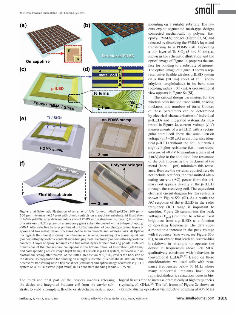
Figure 1 illustrates the designs and main fabrication steps.
The fi rst part involves preparation of μ -ILEDs in formats that
are compatible with techniques for integration by transfer
printing. [ 20 , 21 ] For work described here, thin ( ∼ 6.54 μ m) epitaxial
semiconductor layers (p-GaN/ multiple quantum wells (InGaN/
GaN)/ n-GaN/ buffer layer/ GaN) grown on (0001)-oriented
sapphire substrates serve as active materials. The layer confi g-
uration appears in Figure S1 (Supporting Information, SI). As
shown in the inset optical micrograph, the fabrication, whose
details appear elsewhere, [ 21 ] yields arrays of fully formed InGaN
μ -ILEDs (100 μ m × 100 μ m) with n-type (Cr: 15 nm/ Au: 300 nm)
and p-type ohmic contacts (Ni: 15 nm/ Au: 15 nm) on sapphire
(Figure 1 a). Laser induced lift-off to a silicon wafer (Figure 1 b)
followed by transfer onto a structured substrate (details appear
in Figure S2, SI) of poly(dimethylsiloxane) (PDMS) yields
print-ready devices. Selective transfer printing delivers μ -ILEDs
in desired layouts to a temporary carrier substrate (glass)
coated with a bilayer of epoxy (SU8-2; Microchem.; 1 μ m thick;
ε r (dielectric constant) = 3.2 at 10 MHz; loss tangent = 0.04 at
10 MHz) [ 22 ] / poly(methylmethacrylate) (PMMA A2; Micro-
chem.; 100 nm thick). The second part of the processing uses
adapted versions of procedures described elsewhere, [ 23 ] to yield
patterned interlayer dielectric polymers (epoxy; 6.8 μ m), inter-
connects and inductive coils (Cr (30 nm)/ Au (1000 nm) and top
electrodes (Cr (30 nm)/ Au (500 nm)), with a fi nal, encapsulating
passivation layer of epoxy (1.5 μ m). Here, the rectangular spiral
inductor coil and the straight interconnect lines terminate at the
p- and n-type ohmic contacts, respectively, with a thin ( ∼ 1 μ m)
layer of epoxy to separate these lines at their crossing points.
A schematic illustration of the resulting system is provided in
Figure 1 c. Detailed geometries and dimensions of the metal
interconnects appear in the optical micrograph (top frame)
and the schematic illustration (bottom frame) of Figure 1 d.
Verlag GmbH & Co. KGaA, Weinheim small 2012, 8, No. 18, 2812–2818
Wirelessly Powered Implantable Light-Emitting Systems
Figure 1 . a) Schematic illustration of an array of fully formed, InGaN μ -ILEDs (100 μ m × 100 μ m, thickness ∼ 6.54 μ m) with ohmic contacts on a sapphire substrate. b) Illustration of InGaN μ -ILEDs, after delivery onto a slab of PDMS with a structured surface. c) Illustration of a wireless μ -ILED system on a temporary glass substrate coated with a bi-layer of epoxy/ PMMA. After selective transfer printing of μ -ILEDs, formation of two photopatterned layers of epoxy and two metallization processes defi ne interconnects and wireless coils. d) Optical micrograph (top frame) showing the interconnect scheme, consisting of a planar spiral coil (connected to p-type ohmic contact) and a bridging metal electrode (connected to n-type ohmic contact). A layer of epoxy separates the two metal layers at their crossing points. Detailed dimensions of the planar spiral coil appear in the bottom frame. e) Illustration (left frame) and corresponding optical image (right frame) of a wireless μ -ILED system, retrieved with an elastomeric stamp after removal of the PMMA. Deposition of Ti/ SiO 2 covers the backside of the device, as preparation for bonding on a target substrate. f) Schematic illustration of the process for transferring onto a fl exible sheet (left frame) and optical image of a wireless μ -ILED system on a PET substrate (right frame) in its bent state (bending radius = 0.75 cm).
The third and fi nal part of the process involves releasing
the device and integrated inductor coil from the carrier sub-
strate, to yield a complete, fl exible or stretchable system upon
© 2012 Wiley-VCH Verlag GmbH & Co. KGaA, Weinhesmall 2012, 8, No. 18, 2812–2818
mounting on a suitable substrate. The lay-
outs exploit segmented mesh-type designs
connected mechanically by polymer (i.e.,
epoxy/ PMMA) bridges (Figure S3, SI) and
released by dissolving the PMMA layer and
transferring to a PDMS slab. Depositing
a thin layer of Ti/ SiO 2 (3 nm/ 30 nm), as
shown in the schematic illustration and the
optical image of Figure 1 e, prepares the sur-
face for bonding to a substrate of interest.
The optical image of Figure 1 f shows a rep-
resentative fl exible wireless μ -ILED system
on a thin (50 μ m) sheet of PET (poly-
ethylene terephthalate) in its bent state
(bending radius = 0.5 cm). A cross-sectional
view appears in Figure S4 (SI).
The critical design parameters for the
wireless coils include trace width, spacing,
thickness, and numbers of turns. Choices
of these parameters can be determined
by electrical characterization of individual
μ -ILEDs and integrated systems. As illus-
trated in Figure 2 a, current–voltage ( I – V )
measurements of a μ -ILED with a rectan-
gular spiral coil show the same turn-on
voltage (at I = 20 μ A) as an otherwise iden-
tical μ -ILED without the coil, but with a
slightly higher resistance (i.e., lower slope;
increase of ∼ 0.9 V to maintain a current of
1 mA) due to the additional line resistance
of the coil. Increasing the thickness of the
metal (here ∼ 1 μ m) minimizes this resist-
ance. Because the systems reported here do
not include rectifi ers, the transmitted alter-
nating current (AC) power from the pri-
mary coil appears directly at the μ -ILED,
through the receiving coil. The equivalent
electrical circuit diagram for this system is
shown in Figure S5a (SI). As a result, the
AC response of the μ -ILED in the radio
frequency (RF) range is important to
consider. Figure 2 b summarizes the peak
voltages ( V peak ) required to achieve fi xed
brightness from a μ -ILED, as a function
of operating frequencies. The data show
a monotonic increase in the peak voltage
with frequency (sine wave, see Figure S5b,
SI), to an extent that leads to reverse-bias
breakdown in attempts to operate the
device at frequencies above ∼ 60 MHz,
qualitatively consistent with behaviors in
conventional LEDs. [ 24 , 25 ] Based on these
considerations, we used coils with reso-
nance frequencies below 50 MHz where
many subdermal implants have been
reported; dielectric relaxation losses in bio-
logical tissues tend to increase dramatically at high frequencies
(typically, > 1 GHz). [ 26 ] The left frame of Figure 2 c shows an
example during operation via inductive coupling at 40.9 MHz
2813www.small-journal.comim

R.-H. Kim et al.
28
communications
Figure 2 . a) The current–voltage ( I – V ) characteristics of an individual μ -ILED with and without integrated spiral inductor coils (The spiral coils have dimensions shown in Figure 1 ). b) Peak voltages needed to produce currents of 0.1 mA as a function of operating frequency when operated in an alternating current mode. c) Optical images of a wireless μ -ILED system on a PET substrate powered via inductive coupling at an appropriate resonance frequency in its fl at (left frame) and bent (right frame) state. d) Measured scattering parameter, S11 as a function of bending radius in a concave shape (sample dimension = 4 cm 2 ). e) Measured scattering parameter of inductor coils with reduced dimensions, as a function of bending radius in a concave shape (sample dimension = 1 cm 2 ).
(consistent with separate measurements of an isolated pri-
mary coil (1 turn number, diameter = 5 cm, 12 AWG) with
an external supply (input power = 22.3 dBm, detailed setup
appears in Figure S5c, SI). Flat confi gurations such as this one
offer ideal operating characteristics, but the designs also func-
tion in deformed or bent states. The right frame of Figure 2 c
shows an optical image of a system powered via inductive
coupling (operating frequency = 48.5 MHz, input power
= 23.4 dBm), while sharply bent ( r = 0.75 cm). The observed
increase in required input power is consistent with a corre-
sponding change in the scattering parameter, S11, induced by
concave bending (inset schematic illustration; this deformation
places the device layers in compression), as evaluated on an
isolated coil using a network analyzer (HP 8573D, see Figure
S6a, SI) and a surface mount assembly (BNC, see Figure S6b,
SI). Figure 2 d shows the resonant characteristics of the device
14 www.small-journal.com © 2012 Wiley-VCH Verlag GmbH & Co. KGaA,
of Figure 2 ; the result reveals a systematic
increase and decrease in resonance fre-
quency and peak amplitude, respectively,
with decreasing bending radius. A bending
radius of 1 cm induces a ∼ 21% increase in
resonance frequency and ∼ 90% decrease
in the peak amplitude (Figure S7a, SI),
implying signifi cant reduction in the power
transfer effi ciency and, as a result, the oper-
ating range of the system, even if the pri-
mary coil is adjusted to match the shifted
resonance frequency of the receiver. These
observations can be explained by bending
induced decreases in the inductance, which
are linearly proportional to the area (or
projected area) of a coil enclosed by a cur-
rent loop, according to electromagnetism
theory. [ 27 ] The damped resonance char-
acteristics with bending are due, at least
in part, to increases in the effective dis-
tance between the primary and receiver
coils. Such disadvantages can be relaxed
by reducing the overall dimensions of the
system (also advantageous in implantable
devices), to decrease the sensitivity to the
curvature, in terms of the projected area,
and the effective separation distances, as
shown in Figure S8 (SI). In good agree-
ment with such expectations, the sample
with smaller dimensions (1 cm 2 ) shows no
noticeable dependence of resonance fre-
quency on concave bending (Figure 2 e and
Figure S7b, SI). The peak amplitude shows
trends similar to those of the larger devices,
but with less signifi cant decreases ( ∼ 65%
decrease at a bending radius of 1 cm).
Simple changes in the metal intercon-
nect schemes (i.e., inductor coils) or intro-
duction of stacked geometries represent
other possibilities of interest. For example,
Figure 3 a presents optical images of a
system with four μ -ILEDs, in fl at (inset
image of Figure 3 a) and bent (Figure 3 a, r
(radius of curvature) = 3 cm) states, driven with a single spiral
inductor coil (number of turns = 16, size = 4 cm 2 ) at a fre-
quency of 27.5 MHz. The slight non-uniformity in brightness
is due to an uneven distribution of current that occurs in this
parallel interconnection scheme due to slight variations in
device performance (the μ -ILED indicated by the red arrow
has relatively low output). Uniform emission characteristics
can, nevertheless, by achieved in many cases, as shown in the
inset image of Figure 4 g. The measured scattering parameter,
S11 reveals RF characteristics similar to those of the system
with a single μ -ILED (Figure 2 d) in various bending defor-
mations (concave and convex) as shown in Figure 3 b.
Replacing the straight inductor coils with those that
have serpentine shapes (Figure 3 c) yields systems that can
be stretched, i.e., capable not only of bending but of accom-
modating large strain ( > 1%) deformations with linear
Weinheim small 2012, 8, No. 18, 2812–2818
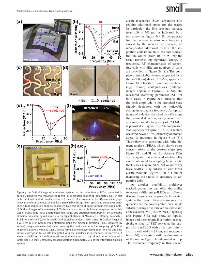
Wirelessly Powered Implantable Light-Emitting Systems
© 2012 Wiley-VCH Verlag GmbH & Co. KGaA, Weinhei
Figure 3 . a) Optical image of a wireless system that includes four μ -ILEDs connected in parallel, powered via inductive coupling. b) Measured scattering parameter, S11 in fl at (solid line) and bent (dashed line) states (concave: blue, convex: red). c) Optical micrograph showing the interconnect scheme for a stretchable design. Both spiral and cross-over metal lines adopt serpentine shapes, separated by a thin layer of epoxy at their crossing points. d) Optical images of a wireless μ -ILED device in a stretchable format integrated on a thin slab of PDMS in its initial unstretched (left frame) and stretched (right frame; ∼ 8% along the direction indicated by red arrows in the fi gure) states. e) Measured scattering parameter, S11 in unstretched (color in black) and stretched (color in red) states. f) Optical image of a wireless μ -ILED system when stretched along the diagonal direction ( ∼ 8%, indicated by arrows). Image was collected while powering the device via inductive coupling. g) Optical image of a stacked wireless μ -ILED device formed by multilayer lamination. The red and blue arrows correspond to μ -ILEDs integrated with the smaller and larger coils, respectively. A wireless μ -ILED system with reduced overall size ( ∼ 1 cm × 1 cm) printed on top of one with larger size ( ∼ 2 cm × 2 cm). h) Measured scattering parameter, S11 of the integrated, stacked system.
small 2012, 8, No. 18, 2812–2818
elastic mechanics. (Such serpentine coils
require additional space for the traces.
In particular, the line spacings increase
from 100 to 300 μ m, as indicated by a
red arrow in Figure 3 c). To compensate
for the increase in resonance frequency
caused by the increase in spacings, we
incorporated additional turns in the ser-
pentine coils (from 16 to 30) and reduced
the line widths (from 100 to 75 μ m); the
result removes any signifi cant change in
frequency. RF characteristics of serpen-
tine coils with different numbers of turns
are provided in Figure S9 (SI). The com-
pleted stretchable device, supported by a
thin ( ∼ 300 μ m) sheet of PDMS, appears in
Figure 3 d in fl at (left frame) and stretched
(right frame) confi gurations (enlarged
images appear in Figure S10a, SI). The
measured scattering parameter (S11 for
both cases in Figure 3 e) indicates that
the peak amplitude in the stretched state
slightly decreases, with no noticeable
change in resonance frequency. An optical
image of a device stretched by ∼ 8% along
the diagonal direction, and powered with
a primary coil at a frequency of 32.4 MHz,
is provided in Figure 3 f ( ∼ 7% compressed
state appears in Figure S10b, SI). Fracture
occurred beyond ∼ 8%, primarily at crossed
edges, as indicated in Figure S10c (SI).
This behavior is consistent with fi nite ele-
ment analysis (FEA), which shows stress
concentrations at the crossed edges (see
Figure S11 and SI text for details). FEA
also suggests that enhanced stretchability
can be obtained by adopting larger metal
thicknesses (Figure S12a, SI) or narrower
trace widths, using substrates with lower
elastic modulus (Figure S12b, SI), and/or
increasing the radius of curvature of ser-
pentine coils.
As another possibility, multilayer
stacked geometries can offer the ability
to operate different μ -ILEDs at different
driving frequencies. Separately fabricated
systems that have different resonance fre-
quencies can be co-integrated on a single
substrate, using an interlayer dielectric and
adhesive of PDMS ( ∼ 50 μ m thick). Figure 3 g
and Figure S13a (SI) show an optical
image and a schematic illustration, respec-
tively. A sheet of PET serves as the sup-
port for a μ -ILED with a fi rst coil (size =
1 cm 2 , metal width = 25 μ m, and turn num-
bers = 60), in a system with the dimensions
of the one in Figure 3 a integrated on top.
The resonance frequency in this stacked
2815www.small-journal.comm

R.-H. Kim et al.
281
communications
geometry is provided in Figure 3 h, showing two weak butnoticeable resonances that match the resonances of indi-
vidual devices before co-integration with slight offsets due to
the mutual coupling between the coils (Figure S13b, SI, shows
the resonance frequency before co-integration).
Solid-state lighting devices have various possible appli-
cations in bio-medicine, ranging from phototherapy (e.g.,
6 www.small-journal.com © 2012 Wiley-VCH Ve
accelerating wound healing and mitigating infection), [ 12–14 ]
to photodynamic drug delivery, [ 15–17 ] to spectroscopic char-
acterization of arterial blood [ 28 ] and cognition, [ 29 ] to optoge-
netics. [ 30 ] Together with recent developments in fl exible
electronics/optoelectronics, the wireless operation capability
introduced here enables such devices to be exploited in
forms designed for these and other purposes. The small sizes
rlag GmbH & Co. KGaA,
of μ -ILEDs are important because they
facilitate passive thermal spreading, and
enable integration using planar processing,
in water-proof forms. Figure 4 a shows
thermal images of a wireless μ -ILED and
integrated coil, operated via inductive cou-
pling at a resonance frequency of ∼ 30 MHz
with different input powers (corresponding
optical images appear in Figure S15a, SI).
The system uses a thin (50 μ m) sheet of
PET as a substrate, mounted on a plastic
plate ( ∼ 1.2 mm thick polystyrene, thermal
conductivity: 0.156 W · m − 1 K − 1 ) for the
measurements. The results show that heat
is mostly generated (ambient temperature
= 21.9 ° C) and localized at the μ -ILED.
As the input power increases (from left
to right images), the peak temperature of
the μ -ILED increases linearly with negli-
gible changes in the temperatures of the
interconnect regions (i.e., inductor coils)
Figure 4 . a) Thermal images of a wireless μ -ILED system on a PET substrate at increasing input power (10.73, 15.72, 20.08, and 28.55 mW from left to right frames). b) Graphical representation of the increase in the peak temperature of the μ -ILED and interconnects (i.e., spiral coils). The surrounding temperature was 21.9 ° C. c) Temperature increases predicted by analytical models and 3D FEA simulations. d) Optical image of a wireless μ -ILED system on PET, completely immersed in water. The image was collected during inductive operation. e) Measured scattering parameter, S11 before and after immersing the system in a PBS solution for two weeks. f) Wireless μ -ILED system, laminated on the sub-dermal region of a mouse model (left frame). The device was driven by inductive coupling. The inset image provides the initial form of the device, integrated on a silk substrate. The optical image in the right frame corresponds to the state after covering the device with the dermis. The image is collected during operation, via inductive coupling through the skin. The exposure time of camera was set to 10 s for ease of viewing of blue light emission from the μ -ILED. g) Image of an animal model with a wireless μ -ILED device implanted under the skin, and on top of the muscle tissue. The inset shows the device before implantation where four μ -ILEDs are integrated on a PET substrate. h) Histological section of tissue at the implant site, excised after 3 weeks (1, corneum; 2, epidermis; 3, dermis, 4, muscular layer).
Weinheim small 2012, 8, No. 18, 2812–2818

Wirelessly Powered Implantable Light-Emitting Systems
as shown in Figure 4 b. Analytical models and FEA of heat
conduction (see SI text for details) reveal the mechanisms for
heat dissipation and provide guidelines to minimize adverse
thermal effects. Analytical solutions for surface tempera-
tures agree well with experiments and FEA (Figure 4 c and
Figure S15b, SI). These models show that the inductor coil
plays a critical role in the thermal transport, without which
the μ -ILED temperature would increase signifi cantly (Figure
4 c). The waterproof characteristics of the wireless μ -ILED
system are demonstrated by results in Figure 4 d and Figure
S16a (SI), which show operation underwater and completely
immersed in phosphate-buffered saline (PBS) solution,
respectively (see Figure S16b, SI). After two weeks immer-
sion of the system in PBS solution, no noticeable changes
were observed in RF characteristics, as shown in Figure 4 e.
In vivo experiments demonstrate explicitly potential
applications in implantable devices. Figure 4 f presents pic-
tures of an animal model with a wireless μ -ILED system
laminated conformally on a sub-dermal region and powered
via inductive coupling with a primary coil at a frequency of
27.6 MHz with (left frame) and without (right frame) the
skin covering in place, where the approximate depth from
the skin was ∼ 3 mm. To facilitate handling and eventual con-
tact, this device used a silk fi lm as a bio-resorbable, water
soluble substrate. Mounting the system on the sub-dermal
surface and then dissolving the silk platform with saline
solution, left only the coil and μ -ILED behind, wrapped
effectively on the tissue by interface water capillary inter-
actions. A more conventional substrate, such as a sheet
of PET, can also be used, as shown in Figure 4 g, although
with somewhat less favorable mechanics. To assess the bio-
compatibility of the system, we examined histological slices
of tissues surrounding the implanted devices (both with
and without encapsulation by a thin layer of PDMS). A
representative image of histological section of tissue at the
implant site, excised after 3 weeks shows absence of any
severe infl ammatory reaction in the neighboring tissues
(Figure 4 h).
These results represent the fi rst demonstrations of
wireless powering in fl exible and stretchable optoelec-
tronic devices, thereby providing some clear implications
for expanded modes of use, particularly in bio-integrated
applications. The RF characteristics of integrated systems
show fi nite, but manageable, dependence on bending and
stretchable deformations, and acceptable thermal behav-
iors, all suggesting a potential for use in implants. The same
procedures and strategies should also be applicable to other
classes of devices that are more complex than those illus-
trated here.
Experimental Section
Fabrication of InGaN μ -ILEDs : The active material stacks were grown on double polished sapphire substrates (2 inch diameter, Cermet Inc.). The composition included undoped GaN (3.8 μ m), a buffer layer, n-type doped GaN (2 μ m), multiple quantum wells (0.14 μ m), and p-type doped GaN (0.2 μ m). After rinsing with diluted HCl (HCl:DI = 1:3) for 5 min to remove the native oxide of
© 2012 Wiley-VCH Verlag Gmsmall 2012, 8, No. 18, 2812–2818
GaN and metal ions, bi-layers of Ni (15 nm)/ Au (15 nm) for cur-rent spreading were formed on p-type GaN by sputter deposition and subsequent photolithography. Annealing in an oxygen and nitrogen atmosphere at a temperature of 500 ° C for 5 min helped to reduce the contact resistances. Next, n-GaN recess regions were formed by chlorine based inductively coupled plasma reactive ion etching (ICP-RIE) through a masking layer of photoresist (AZ nLOF 2070, MicroChem.). Formation of rectangular metal contact pads (Cr (15 nm)/ Au (300 nm) on the n and p-type GaN (25 × 25 μ m 2 ) using electron beam evaporation (Temescal, FC-1800) and photolithography completed the fabrication of arrays of fully formed devices on sapphire. Bonding this substrate to a silicon wafer using an indium (In) and palladium (Pd) chemical alloy prepared the stack for backside exposure with a KrF laser (Intensity = 0.9 J/cm 2 , JPSA Inc.). This process enabled transfer of the devices to the sil-icon, bonded with an In-Pd alloy that forms between some fraction of the In and most of the Pd. Selectively etching of unalloyed In with HCl also removed residual Ga from the laser transfer, to leave isolated structures of In-Pd that hold the devices on the underlying wafer. All of the μ -ILEDs were transferred to a slab of PDMS with embossed features (3 μ m in diameter, 1.2 μ m in height, and 5 μ m in space) on its surface; these structures provide suffi cient adhe-sion for this transfer, but at a suffi ciently weak level to allow effi -cient retrieval with a stamp (relief features with heights and lateral dimensions of 100 μ m) designed for transfer printing. Removing the Pd (for unalloyed Pd) and Cr (adhesion layer) with commercial etchants (Transene) eliminated all of remaining the metal (besides that use for the contacts).
Animal Model Evaluations : All procedures were carried out under approved animal protocols. A female Balb/c mouse was anaesthetized with an intraperitoneal injection of a mix of ket-amine–xylazine. The depth of anesthesia was monitored by palpebral and withdrawal refl exes to confi rm that the animal had reached ‘stage 3’ of anesthesia. Once the animal was lightly anaes-thetized, the back was shaved and cleaned at the incision site with 70% ethanol, followed by a betadine surgical scrub. Once stage 3 was confi rmed, a small longitudinal incision was made through the skin and the sterile implants (ethylene oxide sterilized) were inserted. The incision was closed with a Dexon 5-0 suture. The animal was monitored until ambulatory and given a dose of anal-gesia (Buprenorphine subcutaneously) as soon as surgery was completed. The skin tissue for histology study was harvested after 3 weeks of implantation and washed in PBS, and fi xed in 10% neutral buffered formalin before histological analyses. Samples were dehydrated through a series of graded alcohols, embedded in paraffi n and sectioned at 8 μ m thickness. For histological evalu-ation, sections were deparaffi nized, rehydrated through a series of graded alcohols, and stained with hematoxylin and eosin (H&E).
RF Characterization : Measurements were conducted with a net-work analyzer HP 8573D to determine the return loss, S11 (number of scanning points = 801).
Supporting Information
Supporting Information is available from the Wiley Online Library or from the author.
2817www.small-journal.combH & Co. KGaA, Weinheim

R.-H. Kim et al.
281
communications
[ 1 ] D.-H. Kim , J. Xiao , J. Song , Y. Huang , J. A. Rogers , Adv. Mater. 2010 , 22 , 2108 .
[ 2 ] H. C. Ko , M. P. Stoykovich , J. Song , V. Malyarchuk , W. M. Choi , C.-J. Yu , J. B. Geddes , J. Xiao , S. Wang , Y. Huang , J. A. Rogers , Nature 2008 , 454 , 748 .
[ 3 ] J. A. Rogers , T. Someya , Y. Huang , Science 2010 , 327 , 1603 . [ 4 ] C.-H. Lee , Y.-J. Kim , Y. J. Hong , S.-R. Jeon , S. Bae , B. H. Hong ,
G.-C. Yi , Adv. Mater. 2011 , 23 , 4614 . [ 5 ] R.-H. Kim , D.-H. Kim , J. Xiao , B. H. Kim , S.-I. Park , B. Panilaitis ,
R. Ghaffari , J. Yao , M. Li , Z. Liu , V. Malyarchuk , D. G. Kim , A.-P. Le , R. G. Nuzzo , D. L. Kaplan , F. G. Omenetto , Y. Huang , Z. Kang , J. A. Rogers , Nat. Mater. 2010 , 9 , 929 .
[ 6 ] E. C. Nelson , N. L. Dias , K. P. Bassett , S. N. Dunham , V. Verma , M. Miyake , P. Wiltzius , J. A. Rogers , J. J. Coleman , X. Li , P. V. Braun , Nat. Mater. 2011 , 10 , 676 .
[ 7 ] D.-H. Kim , N. Lu , R. Ma , Y.-S. Kim , R.-H. Kim , S. Wang , J. Wu , S. M. Won , H. Tao , A. Islam , K. J. Yu , T.-I. Kim , R. Chowdhury , M. Ying , L. Xu , M. Li , H.-J. Chung , H. Keum , M. McCormick , P. Liu , Y.-W. Zhang , F. G. Omenetto , Y. Huang , T. Coleman , J. A. Rogers , Science 2011 , 333 , 838 .
[ 8 ] I. Jung , J. Xiao , V. Malyarchuk , C. Lub , M. Li , Z. Liu , J. Yoon , Y. Huang , J. A. Rogers , Proc. Natl. Acad. Sci. USA 2011 , 108 , 1788 .
[ 9 ] T. Sekitani , M. Takamiya , Y. Noguchi , S. Nakano , Y. Kato , T. Sakurai , T. Someya , Nat. Mater. 2007 , 6 , 413 .
[ 10 ] K. D. Wise , D. J. Anderson , J. F. Hetke , D. R. Kipke , K. Najafi , P. IEEE. 2004 , 92 , 76 .
Acknowledgements
This material is based upon work supported in part by a National Security Science and Engineering Faculty Fellowship (J.A.R.), the U.S. Army Research Laboratory and the U.S. Army Research Offi ce under contract number W911 NF-07-1-0618 and by the DARPA-DSO. Funding from the National Science Foundation supported research on the mechanics and processing aspects (NSF Grant Nos. ECCS-0824129 and OISE-1043143). R.-H. K. would like to thank X. Huang and the semiconductor division of Samsung Electronics for invaluable discussions and doctoral fellowships, respectively.
8 www.small-journal.com © 2012 Wiley-VCH
[ 11 ] E. Y. Chow , C.-L. Yang , A. Chlebowski , S. Moon , W. J. Chappell , P. P. Irazoqui , IEEE T. Microw. Theory. 2008 , 56 , 3200 .
[ 12 ] A. V. Corazza , J. Jorge , C. Kurachi , V. S. Bagnato , Photomed. Laser Surg. 2007 , 25 , 102 .
[ 13 ] H. L. Liang , H. T. Whelan , J. T. Eells , M. T. T. Wong-Riley , Neuro-science 2008 , 153 , 963 .
[ 14 ] J. L. N. Bastos , R. F. Z. Lizarelli , N. A. Parizotto , Laser Phys. 2009 , 19 , 1925 .
[ 15 ] C. S. Xu , A. W. N. Leung , L. Liu , X. S. Xia , Laser Phys. Lett. 2010 , 7 , 544 .
[ 16 ] D. Q. Bai , C. M. N. Yow , Y. Tan , E. S. M. Chu , C. S. Xu , Laser Phys. 2010 , 20 , 544 .
[ 17 ] B. P. Timko , T. Dvir , D. S. Kohane , Adv. Mater. 2010 , 22 , 4925 . [ 18 ] S. Waxman , J. Interv. Cardiol. 2008 , 21 , 452 . [ 19 ] C. Balas , Meas. Sci. Technol. 2009 , 20 , 104020 . [ 20 ] S.-I. Park , Y. Xiong , R.-H. Kim , P. Elvikis , M. Meitl , D.-H. Kim , J. Wu ,
J. Yoon , C.-J. Yu , Z. Liu , Y. Huang , K.-C. Hwang , P. Ferreira , X. Li , K. Choquette , J. A. Rogers , Science. 2009 , 325 , 977 .
[ 21 ] a) H.-S. Kim , E. Brueckner , J. Song , Y. Lid , S. Kim , C. Lud , J. Sulkin , K. Choquette , Y. Huang , R. G. Nuzzo , J. A. Rogers , Proc. Natl. Acad. Sci. USA 2011 , 108 , 10072 ; b) T.-i. Kim , Y. H. Jung , J. Song , D. Kim , Y. Li , H.-S. Kim , I.-S. Song , J. J. Wierer , H. A Pao , Y. Huang , J. A. Rogers , Small 2012 , 8 , 1643 .
[ 22 ] J.-H. Jeon , E. J. Inigo , M. T. Reiha , T.-Y. Choi , Y. Lee , S. Mohammadi , L. P. B. Katehi , in 33rd Eur. Microwave Conf. Horizon House Pub-lisher , London, UK 2003 , 53 .
[ 23 ] D.-H. Kim , J.-H. Ahn , W.-M. Choi , H.-S. Kim , T.-H. Kim , J. Song , Y. Y. Huang , L. Zhuangjian , L. Chun , J. A. Rogers , Science 2008 , 320 , 507 .
[ 24 ] H. Kressel , J. K. Butler , in Semiconductor Lasers and Heterojunc-tion LEDs , Academic Press , New York 1977 , p. 73 .
[ 25 ] A. J. pal , R. Österbacka , K.-M. Källman , H. Stubb , Appl. Phys. Lett. 1997 , 70 , 2022 .
[ 26 ] A. N. Laskovski , M. R. Yuce , T. Dissanayake , IEEE Sensors J. 2011 , 11 , 1484 .
[ 27 ] S. Y. Y. Leung , D. C. C. Lam , IEEE T Electron Pa. M. 2007 , 30 , 200 . [ 28 ] J. P. Phillips , R. M. Langford , P. A. Kyriacou , D. P. Jones , Physiol.
Meas. 2008 , 29 , 1383 . [ 29 ] G. Gratton , M. Fabiani , Front. Hum. Neurosci. 2010 , 4 , 1 . [ 30 ] E. S. Boyden , F. Zhang , E. Bamberg , G. Nagel , K. Deisseroth , Nat.
Neurosci. 2005 , 8 , 1264 .
Received: May 2, 2012 Published online: June 29, 2012
Verlag GmbH & Co. KGaA, Weinheim small 2012, 8, No. 18, 2812–2818