Finite Element Modeling of Copper Wire Bonding on a Stacked-Die ...
4
Abstract—Finite element analysis of wire bonding on the overhang of a stacked-die was conducted. The stresses and deflection of the die was determined through the use of the commercially available solver ANSYS. In this study, the finite element model was used to simulate copper wire bonding on a stacked-die application. Copper with its higher hardness required more force to deform. The increase in force generates greater stresses on the die especially on the overhang region. This creates a scenario where the die is under a large amount of stress and may result in cracks. The study aims to determine the stresses and deflections of the die when bonding is carried out on the overhang of the die. It was discovered that the stresses and deflection of the die increases as the distance from the stacked die increases. The study also determined that increasing the thickness of the die leads to decrease in bending stress and deflection of the die. Index Terms—Die deflection, finite element analysis, stacked die, copper wire bonding, overhang region, cracks. I. INTRODUCTION The finite element method (FEM) is a numerical technique which is used to obtain approximate solutions to differential equations [1]-[3]. These differential equations are used to model engineering problems which may involve stress analysis, heat transfer, electromagnetism and fluid flow [1], [4]. As in all finite difference schemes, the finite element method requires that a problem which has been defined in geometrical space (i.e. domain), be subdivided into a finite number of smaller regions [1]. These subdivided regions combined together forms the mesh which is used for calculations. Wire bonding is the most popular interconnection method in the semiconductor packaging industry [5]-[9]. The interconnection provides an electrical path to and from the chip to the substrate which allows transfer of energy and signal. Due to the increase in gold prices over the past two decades, copper, with its greater electrical conductivity, mechanical properties, availability and cost has become a feasible alternative to gold. However, the increased hardness of copper creates a new set of challenges for wire bonding. The large amount of force required to deform a copper Free- Air-Ball (FAB) has raised concerns that it may cause cracks in die especially on the overhang region. Studies have shown that bonding on the overhang can cause issues such as die crack, loop damage and inconsistent Manuscript received March 2, 2013; revised May 2, 2013. Xin Kai Tam, Pooria Pasbakhsh, and N. Q. Guo are with Monash University Sunway Campus, Bandar Sunway, Malaysia (e-mail: pooria. [email protected], [email protected]). Norhazlina Ismail is with MIMOS, Technology Park Malaysia, Kuala Lumpur, Malaysia (e-mail: [email protected]). Kheng Lim Goh is with Newcastle University Singapore Campus, Singapore (e-mail: [email protected]). bump formation due to the bouncing motion of the overhang [10]. Studies have also shown that bonding at different locations of the overhang results in different bending stresses and deflection [11]. Many studies have been conducted which investigates the effect of changing the overhang length on die stress and deflection [10]-[13]. The studies highlighted above also investigated the effect of increasing die thickness on the stress and deflection of the die [10]-[13]. This study aims to determine the stress and deflection of a stacked die by changing the bonding positions instead of changing the dimensions of the overhang. The effect of changing the die thickness will also be investigated in this paper. II. FINITE ELEMENT MODEL The commercially available software UGS NX was used to sketch and construct the model which was then imported into ANSYS, which was used as the simulation program. The geometry of the stacked die which will be used as the basis for the finite element model was provided by a manufacturer (name and data undisclosed for confidentiality). The model consists of 2 dies stacked atop each other. Each of the dies is made out of 2 layers of materials, the bottom layer is silicon whereas the top layer is aluminium. The bottom layer is commonly referred to as the die whereas the top layer is referred to as the bond layer. The geometry is not analyzed as 1 complete body but separated into 2 sections, the first being the bond pad and the second being the remainder of the geometry. Fig. 1. Mesh structure (top view). To allow for sufficient accuracy, a fine mesh must be constructed. The mesh near and around the bond pad must be fine to allow the stresses near the bond pad to be described accurately. Besides that, the mesh near the edge where the 2 dies are joined should also be fine as that is where the bending stress would be highest. The rest of the mesh can be relatively coarse as the stresses and Finite Element Modeling of Copper Wire Bonding on a Stacked-Die in Semiconductor Devices Xin Kai Tam, Pooria Pasbakhsh, N. Q. Guo, Norhazlina Ismail, and Kheng Lim Goh International Journal of Computer Theory and Engineering, Vol. 5, No. 6, December 2013 924 DOI: 10.7763/IJCTE.2013.V5.824
Transcript of Finite Element Modeling of Copper Wire Bonding on a Stacked-Die ...

Abstract—Finite element analysis of wire bonding on the
overhang of a stacked-die was conducted. The stresses and
deflection of the die was determined through the use of the
commercially available solver ANSYS. In this study, the finite
element model was used to simulate copper wire bonding on a
stacked-die application. Copper with its higher hardness
required more force to deform. The increase in force generates
greater stresses on the die especially on the overhang region.
This creates a scenario where the die is under a large amount
of stress and may result in cracks. The study aims to determine
the stresses and deflections of the die when bonding is carried
out on the overhang of the die. It was discovered that the
stresses and deflection of the die increases as the distance from
the stacked die increases. The study also determined that
increasing the thickness of the die leads to decrease in bending
stress and deflection of the die.
Index Terms—Die deflection, finite element analysis, stacked
die, copper wire bonding, overhang region, cracks.
I. INTRODUCTION
The finite element method (FEM) is a numerical
technique which is used to obtain approximate solutions to
differential equations [1]-[3]. These differential equations
are used to model engineering problems which may involve
stress analysis, heat transfer, electromagnetism and fluid
flow [1], [4]. As in all finite difference schemes, the finite
element method requires that a problem which has been
defined in geometrical space (i.e. domain), be subdivided
into a finite number of smaller regions [1]. These subdivided
regions combined together forms the mesh which is used for
calculations.
Wire bonding is the most popular interconnection method
in the semiconductor packaging industry [5]-[9]. The
interconnection provides an electrical path to and from the
chip to the substrate which allows transfer of energy and
signal. Due to the increase in gold prices over the past two
decades, copper, with its greater electrical conductivity,
mechanical properties, availability and cost has become a
feasible alternative to gold. However, the increased hardness
of copper creates a new set of challenges for wire bonding.
The large amount of force required to deform a copper Free-
Air-Ball (FAB) has raised concerns that it may cause cracks
in die especially on the overhang region.
Studies have shown that bonding on the overhang can
cause issues such as die crack, loop damage and inconsistent
Manuscript received March 2, 2013; revised May 2, 2013.
Xin Kai Tam, Pooria Pasbakhsh, and N. Q. Guo are with Monash
University Sunway Campus, Bandar Sunway, Malaysia (e-mail: pooria. [email protected], [email protected]).
Norhazlina Ismail is with MIMOS, Technology Park Malaysia, Kuala
Lumpur, Malaysia (e-mail: [email protected]). Kheng Lim Goh is with Newcastle University Singapore Campus,
Singapore (e-mail: [email protected]).
bump formation due to the bouncing motion of the overhang
[10]. Studies have also shown that bonding at different
locations of the overhang results in different bending
stresses and deflection [11]. Many studies have been
conducted which investigates the effect of changing the
overhang length on die stress and deflection [10]-[13]. The
studies highlighted above also investigated the effect of
increasing die thickness on the stress and deflection of the
die [10]-[13]. This study aims to determine the stress and
deflection of a stacked die by changing the bonding
positions instead of changing the dimensions of the
overhang. The effect of changing the die thickness will also
be investigated in this paper.
II. FINITE ELEMENT MODEL
The commercially available software UGS NX was used
to sketch and construct the model which was then imported
into ANSYS, which was used as the simulation program.
The geometry of the stacked die which will be used as the
basis for the finite element model was provided by a
manufacturer (name and data undisclosed for
confidentiality). The model consists of 2 dies stacked atop
each other. Each of the dies is made out of 2 layers of
materials, the bottom layer is silicon whereas the top layer is
aluminium. The bottom layer is commonly referred to as the
die whereas the top layer is referred to as the bond layer.
The geometry is not analyzed as 1 complete body but
separated into 2 sections, the first being the bond pad and
the second being the remainder of the geometry.
Fig. 1. Mesh structure (top view).
To allow for sufficient accuracy, a fine mesh must be
constructed. The mesh near and around the bond pad must
be fine to allow the stresses near the bond pad to be
described accurately. Besides that, the mesh near the edge
where the 2 dies are joined should also be fine as that is
where the bending stress would be highest. The rest of the
mesh can be relatively coarse as the stresses and
Finite Element Modeling of Copper Wire Bonding on a
Stacked-Die in Semiconductor Devices
Xin Kai Tam, Pooria Pasbakhsh, N. Q. Guo, Norhazlina Ismail, and Kheng Lim Goh
International Journal of Computer Theory and Engineering, Vol. 5, No. 6, December 2013
924DOI: 10.7763/IJCTE.2013.V5.824

deformations of those areas are not as important. The default
mesh options are used but edge sizing is used near the bond
pad to reduce the size of the mesh near the bond pad. A
contact region sizing was used on the contact region
between the aluminium layer of the bottom die and the top
die. The relevance setting was set to maximum (i.e. +100).
The relevance setting for the entire mesh was also set to
+100 to increase the overall mesh density. Fig. 1 and Fig. 2
shows the top and bottom view of the mesh respectively. As
can be seen from Fig. 2, the mesh density where the dies are
connected is higher compared to that at the top of the die.
Fig. 2. Mesh structure (bottom view).
The bottom surface of the die is constrained using a fixed
support. It is also possible to use a compression-only
support to fix the bottom surface. It may result in more
accurate representation of the actual wire bonding process
but the increase in simulation time would be significant. A
force of 80g is applied uniformly over the whole bond pad
to simulate the force of the FAB impacting the bond pad.
During actual wire bonding, the FAB will be compressed on
to the bond pad by a capillary resulting in the deformation of
the FAB and bond pad. The assumption that the force is
acting over the entire bond pad is however an acceptable
one as pointed out in a study by Chen et al. [15]. The study
showed that miniaturization of stacked die packages have
resulted in a decrease in bond pad sizes such that the size of
the bond pad is nearly similar to that of the deformed FAB.
Fig. 3. Schematic diagram of bonding positions.
The material properties of the silicon and aluminium
layers were obtained from literature. The die is made of
silicon whereas the bond layer is made of aluminium. A
linear elastic model is used for both these materials. The
solvers for von-Mises stress and total deflection is used in
the simulation. The bonding positions which will be used in
the simulation are shown in Fig. 3. In total, 30 bonding
positions will be tested, 25 on the overhang region and 5 on
the stacked die region. The 5 bonding positions on the
stacked die is to provide comparison and to show the
difference in stress distribution when bonding is carried out
off the overhang. The final step of the simulation involved
increasing the die thickness and determining the stress and
deflection at bond positions 1 and 5 for 2 extra die
thicknesses (i.e. 150 microns and 200 microns).
A grid independency test was also carried out for the
mesh which was used to perform the simulations. A grid
independency test is a test which determines if a certain
mesh size is able to produce sufficiently accurate results
when compared to a finer mesh size. The results of the grid
independency test are shown in Table I. It is shown that the
percentage difference of using the coarse mesh is less than
10% against the fine mesh for stress and the percentage
difference in deflection is less than 1%. This is acceptable as
decreasing the mesh size significantly increases simulation
time.
The simulation was only carried out on one side of the
overhang as the results for the opposite side of the overhang
should be a mirror image of the results. The bonding
positions are determined using horizontal and vertical
offsets which are shown in Fig. 3. The horizontal offset is
increased in 0.4mm increments whereas the vertical offset is
increased by 0.2mm increments.
TABLE I: GRID INDEPENDENCY TEST RESULTS
Nodes Stress
(MPa)
Deflection
(microns)
Percentage Difference (%)
Stress Deflection
99739 599.6 73.766 - -
224322 632.7 73.891 5.23 0.17
288209 550.9 74.076 8.84 0.42
One important point to note is the use of automatic
contact regions within ANSYS to generate the contact
regions between the dies and bond layers. The program
automatically created bonded contact regions between all
the surfaces which were adjacent to each other. However,
due to the extremely small thickness of the aluminium layer,
a contact region was also created between the bottom die
and the top die. This contact region was deleted.
III. RESULTS AND DISCUSSION
Graphs of stress versus horizontal offset and stress versus
vertical offset are plotted and shown in Fig. 4 and Fig. 5.
The values for bonding on the stacked die are also included
in Fig. 4 for comparison. It can be seen that the decrease in
stress is very abrupt when the horizontal offset is first
increased. The rate at which the stress decreases evens out
as the horizontal offset is increased by between 1.3 to
1.7mm. This shows that further increasing the horizontal
offset would not result in much change in stress. In fact,
some of the values of stresses at a horizontal offset of
1.7mm are higher than that at 1.3mm. This is partly due to
numerical errors caused by the program but it also indicates
that the stress is already at a minimum for that vertical offset.
This is more clearly shown in Fig. 5 where the orange line
and pink line are intersecting each other. Fig. 5 shows that
decrease in stress is nearly linear as the vertical offset is
increased. The slopes of the curve also indicate that the rate
at which the stress decreases is similar regardless of the
horizontal offset of the bond pad.
International Journal of Computer Theory and Engineering, Vol. 5, No. 6, December 2013
925
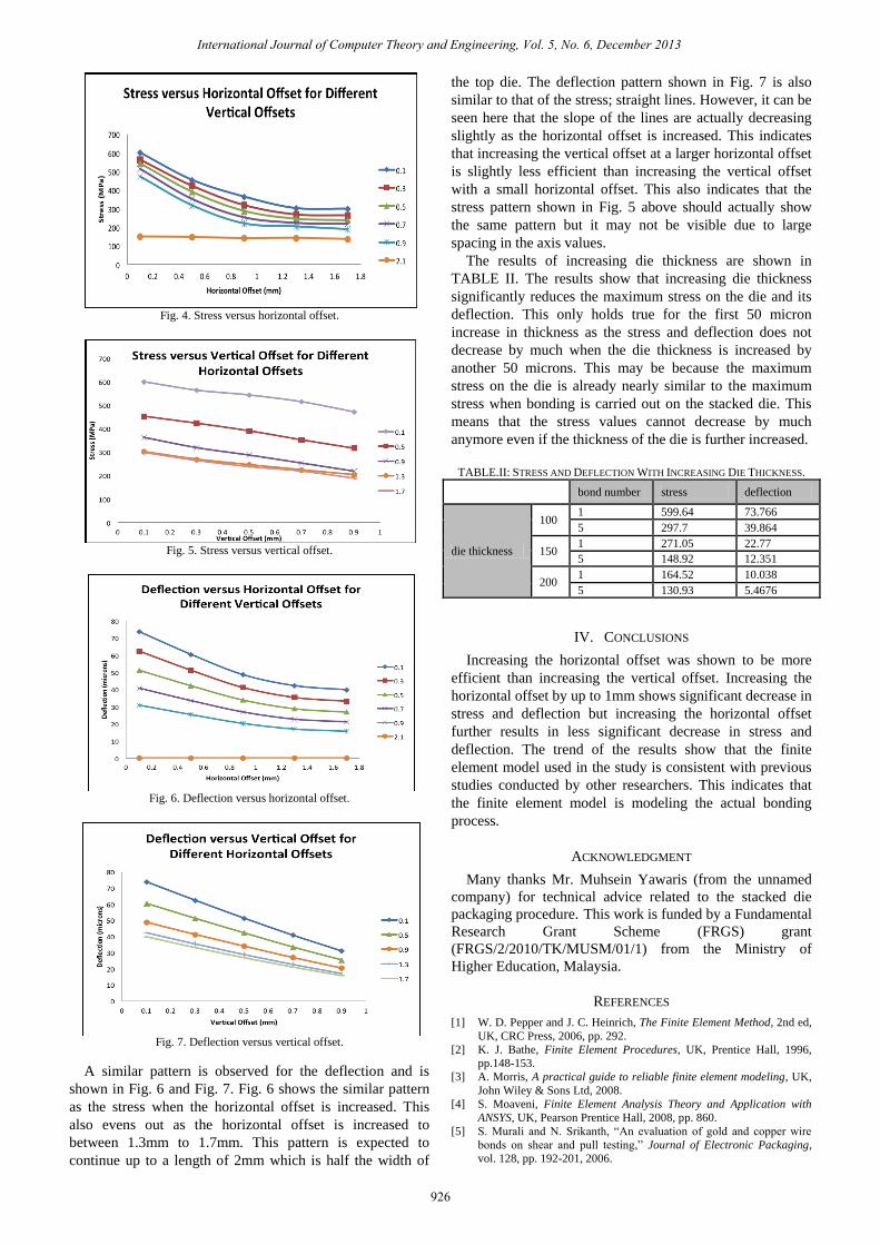
Fig. 4. Stress versus horizontal offset.
Fig. 5. Stress versus vertical offset.
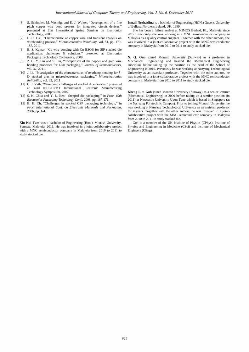
Fig. 6. Deflection versus horizontal offset.
Fig. 7. Deflection versus vertical offset.
A similar pattern is observed for the deflection and is
shown in Fig. 6 and Fig. 7. Fig. 6 shows the similar pattern
as the stress when the horizontal offset is increased. This
also evens out as the horizontal offset is increased to
between 1.3mm to 1.7mm. This pattern is expected to
continue up to a length of 2mm which is half the width of
International Journal of Computer Theory and Engineering, Vol. 5, No. 6, December 2013
926
the top die. The deflection pattern shown in Fig. 7 is also
similar to that of the stress; straight lines. However, it can be
seen here that the slope of the lines are actually decreasing
slightly as the horizontal offset is increased. This indicates
that increasing the vertical offset at a larger horizontal offset
is slightly less efficient than increasing the vertical offset
with a small horizontal offset. This also indicates that the
stress pattern shown in Fig. 5 above should actually show
the same pattern but it may not be visible due to large
spacing in the axis values.
The results of increasing die thickness are shown in
TABLE II. The results show that increasing die thickness
significantly reduces the maximum stress on the die and its
deflection. This only holds true for the first 50 micron
increase in thickness as the stress and deflection does not
decrease by much when the die thickness is increased by
another 50 microns. This may be because the maximum
stress on the die is already nearly similar to the maximum
stress when bonding is carried out on the stacked die. This
means that the stress values cannot decrease by much
anymore even if the thickness of the die is further increased.
TABLE.II: STRESS AND DEFLECTION WITH INCREASING DIE THICKNESS.
bond number stress deflection
die thickness
100 1 599.64 73.766
5 297.7 39.864
150 1 271.05 22.77
5 148.92 12.351
200 1 164.52 10.038
5 130.93 5.4676
IV. CONCLUSIONS
Increasing the horizontal offset was shown to be more
efficient than increasing the vertical offset. Increasing the
horizontal offset by up to 1mm shows significant decrease in
stress and deflection but increasing the horizontal offset
further results in less significant decrease in stress and
deflection. The trend of the results show that the finite
element model used in the study is consistent with previous
studies conducted by other researchers. This indicates that
the finite element model is modeling the actual bonding
process.
ACKNOWLEDGMENT
Many thanks Mr. Muhsein Yawaris (from the unnamed
company) for technical advice related to the stacked die
packaging procedure. This work is funded by a Fundamental
Research Grant Scheme (FRGS) grant
(FRGS/2/2010/TK/MUSM/01/1) from the Ministry of
Higher Education, Malaysia.
REFERENCES
[1] W. D. Pepper and J. C. Heinrich, The Finite Element Method, 2nd ed,
UK, CRC Press, 2006, pp. 292.
[2] K. J. Bathe, Finite Element Procedures, UK, Prentice Hall, 1996,
pp.148-153.
[3] A. Morris, A practical guide to reliable finite element modeling, UK,
John Wiley & Sons Ltd, 2008.
[4] S. Moaveni, Finite Element Analysis Theory and Application with
ANSYS, UK, Pearson Prentice Hall, 2008, pp. 860.
[5] S. Murali and N. Srikanth, “An evaluation of gold and copper wire
bonds on shear and pull testing,” Journal of Electronic Packaging,
vol. 128, pp. 192-201, 2006.
[6] S. Schindler, M. Wohnig, and K.-J. Wolter, “Development of a fine
pitch copper wire bond process for integrated circuit devices,”
presented at 31st International Spring Seminar on Electronics Technology, 2008.
[7] H.-C. Hsu, “Characteristic of copper wire and transient analysis on
wirebonding process,” Microelectronics Reliability, vol. 51, pp. 179-187, 2011.
[8] B. S. Kumar, “Cu wire bonding with Cu BSOB for SIP stacked die
application: challenges & solutions,” presented at Electronics Packaging Technology Conference, 2009.
[9] Z. C. Y. Liu and S. Liu, “Comparison of the copper and gold wire
bonding processes for LED packaging,” Journal of Semiconductors, vol. 32, 2011.
[10] J. Li, “Investigation of the characteristics of overhang bonding for 3-
D stacked dies in microelectronics packaging,” Microelectronics Reliability, vol. 32, 2011.
[11] C. J. Vath, “Wire bond challenges of stacked dice devices,” presented
at 32nd IEEE/CPMT International Electronic Manufacturing Technology Symposium, 2007.
Xin Kai Tam was a bachelor of Engineering (Hon.), Monash University, Sunway, Malaysia, 2011. He was involved in a joint-collaborative project
with a MNC semiconductor company in Malaysia from 2010 to 2011 to
study stacked die.
Ismail Norhazlina is a bachelor of Engineering (HON.) Queens University
of Belfast, Northern Ireland, UK, 1999.
She has been a failure analyst at MIMOS Berhad, KL, Malaysia since 2012. Previously she was working in a MNC semiconductor company in
Malaysia as a quality control engineer. Together with the other authors, she
was involved in a joint-collaborative project with the MNC semiconductor company in Malaysia from 2010 to 2011 to study stacked die.
N. Q. Guo joined Monash University (Sunway) as a professor in
Mechanical Engineering and headed the Mechanical Engineering
Discipline before taking up the position as the head of the School of Engineering in 2010. Previously he was working at Nanyang Technological
University as an associate professor. Together with the other authors, he
was involved in a joint-collaborative project with the MNC semiconductor company in Malaysia from 2010 to 2011 to study stacked die.
Kheng Lim Goh joined Monash University (Sunway) as a senior lecturer
(Mechanical Engineering) in 2009 before taking up a similar position (in
2011) at Newcastle University Upon Tyne which is based in Singapore (at the Nanyang Polytechnic Campus). Prior to joining Monash University, he
was working at Nanyang Technological University as an assistant professor
for 4 years. Together with the other authors, he was involved in a joint-
collaborative project with the MNC semiconductor company in Malaysia
from 2010 to 2011 to study stacked die.
Goh is a member of the UK Institute of Physics (CPhys), Institute of Physics and Engineering in Medicine (CSci) and Institute of Mechanical
Engineers (CEng).
International Journal of Computer Theory and Engineering, Vol. 5, No. 6, December 2013
927
[12] S. K. Chua and Y. L. Neo, “Stepped die packaging,” in Proc. 10th
Electronics Packaging Technology Conf., 2008, pp. 167-171.[13] B. H. Oh, “Challenges in stacked CSP packaging technology,” in
Proc. International Conf. on Electronic Materials and Packaging,
2006, pp. 1-4.


![Accelerated SLID Bonding Using Thin Multi-Layer Copper ...€¦ · surfaces prior to bonding [2]. The Georgia Tech-Packaging Research Center recently made pioneering advances and](https://static.fdocuments.net/doc/165x107/5ed15cbbd2340461e35d3940/accelerated-slid-bonding-using-thin-multi-layer-copper-surfaces-prior-to-bonding.jpg)