
Final Report: Processor-ln-Memory (PIM) Based ... · for PetaFlops Potential Massively Parallel...
56
NASA-CR-202_32 PIMs for Petaflops / Final Report: Processor-ln-Memory (PIM) Based Architectures for PetaFlops Potential Massively Parallel Processing NASA Grant NAG 5-2998 July 15,1996 Dr. Peter M. Kogge McCourtney Professor of Computer Science and Engineering IEEE Fellow, IBM Fellow (retired) University of Notre Dame Notre Dame, IN 46556 219-631-6763 fax: 219-631-9260 email: [email protected] https://ntrs.nasa.gov/search.jsp?R=19970001424 2019-02-01T20:25:16+00:00Z
Transcript of Final Report: Processor-ln-Memory (PIM) Based ... · for PetaFlops Potential Massively Parallel...

NASA-CR-202_32
PIMs for Petaflops
/
Final Report:
Processor-ln-Memory (PIM) Based Architectures
for PetaFlops Potential
Massively Parallel ProcessingNASA Grant NAG 5-2998
July 15,1996
Dr. Peter M. Kogge
McCourtney Professor of Computer Science and Engineering
IEEE Fellow, IBM Fellow (retired)
University of Notre Dame
Notre Dame, IN 46556
219-631-6763
fax: 219-631-9260
email: [email protected]
https://ntrs.nasa.gov/search.jsp?R=19970001424 2019-02-01T20:25:16+00:00Z

PIMs for Petaflops
Final Report:
Processor-In-Memory (PIM) Based Architectures
for PetaFlops Potential
Massively Parallel ProcessingNASA Grant NAG 5-2998
July 15, 1996
Dr. Peter M. Kogge
McCourtney Professor of Computer Science and Engineering
IEEE Fellow, IBM Fellow (retired)
University of Notre Dame
Notre Dame, IN 46556219-631-6763
fax: 219-631-9260
email: [email protected]

1. Introduction: ............................................................. Page 1
2. The Problem Addressed by this Study: ................................ Page 1
3. Study Objectives and Approach: ....................................... Page 3
4. PIM Background ......................................................... Page 4
5. Overview of Results ..................................................... Page 6
5.1 Interactions with Petaflops community ................................ Page 6
5.2 Applications Requirements ........................................... Page 7
5.3 PIM Technology Design Space ....................................... Page 10
5.4 PIM Architectural Design Space ...................................... Page 13
5.4.1 Processor Node General Architecture ........................... Page 14
5.4.2 Choice for Processing Logic ..................................... Page 16
5.4.3 Floorplanning by Tiling .......................................... Page 19
5.4,4 Adding Off Chip Interfaces ...................................... Page 20
5.5 System Configurations ............................................... Page 22
5.5.1 Chip Counts for a Petafiop System .............................. Page 23
5.5.2 Area and Logic Fraction ......................................... Page 24
5.5.3 Internal Parallelism .............................................. Page 24
5.5.4 Off Chip Contacts ............................................... Page 25
5.5.5 3D Stacks ....................................................... Page 26
5.5.6 System Power .................................................. Page 26
5.6 Comparisons to Current Practice Extended ........................... Page 26
5.7 Simplifying the Operating System Support ............................ Page 27
5.8 Other Key Results .................................................... Page 28
6. Importance of the Findings and Future Directions ...................... Page 29
7. Relevant Publications: .................................................. Page 31
Appendix A: Preprint "Pursuing a Petaflop..."
Appendix B: PAWS Draft Proceedings, Section 8.1, "Component Characterization"

PIMs for Petaflops
1. Introduction:
The report summarizes the work performed at the University of Notre Dame under NASA
Grant NAG 5-2998 from July 15, 1995 through July 14, 1996. Researchers involved in the work
included the PI, Dr. Peter M. Kogge, and three graduate students under his direction in the
Computer Science and Engineering Department: Stephen Dartt, Costin Iancu, and Lakshmi
Narayanaswany.
The organization of this report is as follows. Section 2 is a summary of the problem addressed
by this work. Section 3 is a summary of the project's objectives and approach. Section 4
summarizes PIM technology briefly. Section 5 overviews the main results of the work. Section 6
then discusses the importance of the results and future directions.
Also attached to this report are copies of several technical reports and publications whose
contents directly reflect results developed during this study. This includes a paper that will be
published in the Frontiers of Massively Parallel Computing Conference in Annapolis, MD in
October, 1996. Several other papers are under preparation for submission for formal publication.
All these published papers will acknowledge the support received from this grant.
2. The Problem Addressed by this Study:
With the achievement of real teraflops (1012 floating point operations per second, TF)
computers in sight, it is now time to begin focusing on the next major level of processing: a
petaflop (1015 operations PF) per second. Such machines could compute in 15 minutes what
would take a TF machine over 10 days, or a high end gigaflops (109 operations per second - GF)
machine over 30 years. As was shown in the 1994 Cal Tech Workshop on Petaflops Computing,
and the 1995 Petaflops Frontiers Workshop (both including sponsorship bv NASA, with
significant organizational responsibilities by Dr. Thomas Sterling, then of NASA CESDIS), there
are a great many applications of significant scientific and economic benefit that would be opened
up by such levels of computing. Further, the same technology that would enable these levels of
computing would also enable placing today's teraflops machine room in a desk environment, and
today's gigaflops rack of computers into handholdable packages. Both of these size reductions
have huge potential societal impacts, especially as we move to a more and more mobile society
Page 1
PIMs for Petaflops
where portable communications and information exchange of all sorts over gigabit networks will
become the bedrock of the business environment.
The major problem with achieving such levels of performance today is cost. Even using the
best of today's technology would require 10's of millions of chips and literally 10's of billions of
dollars to reach a petaflops machine. This is simply not a viable option. However, projecting
technology ahead, as was done in the 1994 Workshop, indicates that within approximately 20
years the state of the art in VLSI should make such machines feasible, with at least three different
computer architectures reasonable candidates.
Given the above result, why should any attention be paid in 1995 or 1996 to petaflops level
machines? The answer is two-fold. First, all the architectures proposed in the 1994 Workshop for
petaflops were truly Massively Parallel Processors (MPP), an approach becoming widespread at
the very high end of existing machines but proving tough to handle, and virtually unstudied for
lower level everyday applications, and not at the level of 10s to 100s of thousands of
semi-independent processors (non trivial non SIMD engines). Second, the architecture with the
greatest initial potential in terms of minimal chips, and thus cost, is one where multiple entire,
relatively simple but not trivial, computers are integrated onto single chips that combine the state
of the art in memory densiW with very significant amounts of high speed logic. For obvious
reasons the architecture of such chips is becoming known as Processing-In-Memory (PIM).
In today's world of superscalar, superpipelined, multiple execution unit, 10 million+ transistor
single CPU microprocessor designs, both of these observations are so far out of the mass
production norm that without a jump-start, neither will mature to the levels needed by the time the
technology is ready for a petaflops. Consequently, what is needed is a believable roadmap
projecting no only what appropriate PIM architectures might look like 20 years from now, but
what are the intermediate stops along the way. This includes what can be done with today's
technology, or the technology of 1998 or 2001, for example, to implement such PIM-based MPP
machines, and how does this compare with where the conventional trends will take us.
Very preliminary projections [8, 9, 10] based on the first real PIM chips such as EXECUBE [5,
7, 11] indicate that in terms of silicon usage, PIM offers at least an order of ma_itude better
advantage than other approaches. Given the potential simplicity of PIM designs versus modem
Page 2

PIMs for Petaflops
microprocessors(EXECUBE costlessthan$5M to developversushundredsof millions for the
very leadingedgeconventionalchips),this meansthat PIM-basedMPPshavethepotentialto not
only affectveryhigh endcomputing20yearsfrom now,but radically changethe wav we embed
very high levels of processing in the mobile world of the late 1990s'!
3. Study Objectives and Approach:
Given the above observations, the goal of this study was to develop an initial roadmap to
achieving petaflop using PIM-based MPPs, with a emphasis on early and continuing design points
that would identify both the technologies needed to achieve a petaflop, and intermediate
applications, including embedded ones of interest to NASA, that would provide the economic
impetus to fund more fully the development of those technologies.
In particular, as described in the original proposal this work was to consist of the following:
1.Interactions with applications experts and the developing petaflops research community (both
within and outside of NASA) to validate that architectural choices are not only chip-efficient, but
also are reasonable targets for real applications. Such applications will include not only petaflops
level ones, but lower performance, especially embedded, applications which max be uniquely
enabled by PIMs.
2.Use of existing CMOS VLSI technology trends to identify the design spaces, in terms of amount
of memory and logic, possible for PIM chips at regular intervals over the next 20 years.
Constraints such as off chip contacts, power dissipation, die size for economic production, etc.,
were all a part of this characterization.
3.Architectural tradeoffs to identify which type of individual processor node architectures best
utilize the silicon and memory bandwidth present on a VLSI chip at each of the above time
intervals. This included not only existing architectures (from the very simple to the more
complex), but also novel ones that more fully utilize chips with significant memor, and logic.
4.Development of candidate MPP system architectures using potential PIM chips identified above,
and derivation of key characteristics such as limits and ease of scalability, number of chips,
power, needed runtime and support software, etc.
Page 3

PIMsfor Petaflops
Thestatementof work alsoassumedparticipationattwo workshopsonpetaflopsovertheyear
of study.
4. PIM Background
The thesisbehind PIM is that manyof the problemsfacing very high performanceMPP
computersstemfrom the "traditional"vonNeumannbottleneck,andhow we haveapproachedit.
FortechnologyandcostreasonswehavehistoricallyseparatedmemorypartsandCPUlogic parts.
With theadventof CMOSmicroprocessorswith veryhighperformancepipelinedandsuperscalar
architectures,individual CPU core performancelevels have gone through rapid acceleration.
requiringeverincreasingamountsof bandwidthfrom thememorysubsystem.Theserateshavefar
exceededthe bandwidthcapabilitiesof ourdensestDRAM (DynamicRandomAccess/Viemory)
memory parts (needed to control system costs), and the gap will continue to widen over time. The
net result is architectural complexity: memory hierarchies are introduced to provide the bandwidth.
which in turn drives cost and the software complexity needed to address these hierarchies
efficiently, especially in an MPP environment.
The PIM technology is emerging to counter this fundamental defect - namely the combination
on one chip of both dense DRAM memory and very significant amounts of logic. This capabilit)'
permits new architectures to place computing either right next to, or even inside of. the memo_
macros, where there are huge amounts of raw memory bandwidth.
Many chips today combine logic with some form of memory. At one extreme most modern
microprocessors combine millions of transistors of logic with a few tens of KB (Kilo Bytes) of
SRAM (for caches). At the other extreme, most conventional DRAMs combine MBs (Mega Bytes)
of memory with a few thousands of transistors for address decoding for the internal arrays.
latching at the sense amps, and multiplexing to drive the data lines.
PIM chips fall in the middle. They combine large amounts of both memory and logic.
However, the key feature that distinguishes them from the conventional chips is that they represent
potentially self-contained designs where all the processing functions and all the memory for that
processing for one or more nodes are on the same chip. This self-contained characteristic has
several key consequences:
Page 4

PIMsfor Petaflops
• It is possible to conceive of a single part type scaleable MPP design where additional
computational resources are added by adding more of the same kind of chips (much as today we
add more memory to PCs via plug in SIMMs).
• This in turn permits consideration of novel 3D packaging techniques which both reduce overall
system costs and provide shorter chip to chip paths, reducing the other killer of MPP
performance - latency.
Placing the processing logic next to the memory permits a huge increase in the percent of raw
memory bandwidth that can be utilized from the memory arrays over today, where at best a few
percent of the total bandwidth is presented to the off chip pins. This can reduce or eliminate the
need for complex caching and other tricks in the design of the processing logic - again reducing
both cost and latency.
• Eliminating from the processing chips the need for often hundreds of pins to support a memory
hierarchy means that these same pins can be used to perform something computationally useful
- namely communication with other processing nodes.
• Moving multiple processing nodes to a single chip also allows consideration of new
architectural techniques such as mixed SIMD and MIMD processing, very high bandwidth
memory to memory transfers, and "in the memory array" processing, all of which in turn should
be useful to significantly reduce application program complexity.
• A combination of all these techniques offer the potential for greatly reduced power dissipation
per unit of performance. Simplicity in logic means that there is less logic to burn power;
reduced pin count to support memory hierarchies yields less power, and higher memory
bandwidth and lower latency next to the processing logic implies the potential for lower clock
rates - again lowering power.
The first such PIM chip to utilize state of the art dense DRAM, EXECUBE [5, 8, 11],
integrated onto a 4 Mbit DRAM chip 8 complete CPUs configured in a 3 dimensional bina_"
hypercube, and was used as a one chip type building block for MPPs of both MIMD and SIMD
organization. On a chip basis, it was up to 10 times more efficient than traditional techniques in
terms of performance per chip over an entire system. At 2.7 watts typical dissipation, it also
demonstrated extraordinary performance per watt (again on a system wide basis) for its time frame
and implementation technology.
Page 5

PIMsfor Petaflops
5.Overview of Results
Very significantprogresswasmadeon all of the topics listed in Section3. The following
subsectionsoverviewtheresults.In manycasesmore resultsareavailablein theattachedreports,
with other results to be reported in documents currently under preparation. The order of
presentation starts with a brief review of the interactions held with the petaflops community; these
meetings will then be referenced in later sections when outputs from them directly affected the
results of the study. Following this is a summary of what was learned about petaflops applications
requirements, the design space offered by the projected CMOS trends, the potential high level
architecture of a strawman PIM chip was investigated, and then how that architecture could
evolve into a complete system. This latter section also addresses some issues associated with
software: both tools and runtime.
5.1 Interactions with Petaflops community
As part of this effort, we participated in not two, but three different petaflops related
workshops:
1.Petaflops Summer Study on Algorithms in Bodega Bay, CA in August 1996. At this workshop
we presented some early results from the PIM projections spreadsheet model described later,
with emphasis on the significant advantages that PIM held, along with the characteristics that a
PIM-based petaflops machine might have, in particular a de_ee of parallelism in the 160,000+
range. Feedback from this study provided more insight into exactly how much primary and
secondary memory, I/O bandwidth, and expected running time were reasonable to assume for
petaflops applications.
2.Petaflops Architecture Workshop in Oxnard, CA, in April 1996. The results of this study were
used in two separate presentations at this workshop. First, the requirements learned from the
Bodega Bay workshop were presented early in the workshop to provide an overview of what was
required by an yvpetaflops capable machine, not just the PIM approach. Second, a more detailed
presentation was made on the PIM strawman architecture described above, with more realistic
CMOS technology constraints taken into account. Outputs to this study were a growth in the
architectural design space for PIM chips, and a recognition that PIM could be applied in much
more general fashions than had been earlier anticipated.
Page 6

PIMs for Petaflops
3.PetaflopsSystemSoftware Workshop in BodegaBay in June 1996. Although no formal
presentationson PIMs were made at the workshop, it becameclear that the PkM approach,
especiallywhencoupledwith its insertioninto a conventionalsystemas "smartmemory,"held
the promise of greatly simplified software (both tools and runtime support) over the more
traditionalapproachesdiscussedat theconference,andtheproblemsthatthoseapproachesfaced
whenscaledto thepetaflopsregion.
Finally, a meetingis plannedin earlyAugustwith interestedgovernmentagenciesasto the
nextstepfor thedevelopmentof petaflopsmachinesin general,andhow PIM mightplaya role in
that.
5.2ApplicationsRequirements
Beforeonecansizea machineof _ possiblearchitectureto reachapetaflop,onemusthave
first a set of approximaterequirementsto work with. The 1995SummerPetaflopsAlgorithm
Workshopin BodegaBay,CA providedjust sucha basisby summarizingfrom over30 possible
applicationsthat would profit from a petaflopmachinea varietyof characteristics,includingthe
runningtime for atypicalexecution(whenona petafloppersecondmachine),theprimarystorage
(memory)neededto supporttheapplication,thesecondarystorage(disk) needed,andtheI/O rate.
Giventhe costof memoo'evenin the 2010s,theprimarystoragefigureis mosttelling. Figure 1
diagramsthisasascatterplot whereeachdotcorrespondsto aparticularapplication,positionedon
thegraphasa function of its executiontime for a singlerun (in seconds,on x-axis) andprimal
memory(in GB, on y-axis).Threedifferent symbolsareusedhere:onefor applicationsrequiring
lessthan100seconds(about2 minutes),onefor applicationswith executiontimesbetween100
and10,000seconds(about3hours),andonefor in excessof that.
As can be seen, the execution time spanseight orders of magnitude,and the memorv
requirementsspansix ordersof magnitude(1E3GB is aterabyteTB; 1E6GB is a petabytePB).
Therearesignificantnumbersof applicationsin eachof thetime frames,but no clearcorrelation
betweenrunningtime andprimarymemory.
Figure 2 perhapsgives better insight into the questionof "how much primary memory is
enough?"Roughlyhalf theapplicationscouldbesatisfiedby aTB, and80%by 30TB. This latter
numberof 30TB alsocorrespondswell to anestimatemadeatthe 1994PetaflopsWorkshopthat
Page7

PIMsfor Petaflops
rn(.9v
O
E
&.,
E
13..
1E+06
1E+05
1E+04
1E+03
1E+02
1E+01
1E+00
1E+00
i*
............................................................. _ ..........................................._.................._ ....................., ................
i A i *
...............................................................- ..........,,,,..._.!.....................-..................,_.................._ .................
..................................e,.........................{................_ .....................................................................................
...... • ........._ ..................................................A....................."......._............................................................
1E+01 1E+02 1E+03 1E+04 1E+05 1E+06 1E+07 1E*08
Individual Application Runtime @ 1 Petaflop (seconds)Figure 1. Petaflops Applications: Runtime vs Primary Memory Requirements
100
¢-._o
O
Q.{3.
<
O
c-"
0
8O
60
4O
2O
0
1 E+O0
1 I I I
1E+01 1E+02 1E+03 1E+04 1E+05
Primary Memory Size (GB)
1E+06
Figure 2. Percent of Bodega Bay Petaflop applications requiring different memory sizes.
Page 8

PIMsfor Petaflops
10,000.000
1,000.000
100.000
0
10.000
1.0000
0.100
0.010
0.001
................................. • .................................... ,..................................... _.................................... _ ............................... •i ................................
i
........................................................................................................... !.lB .............................. _ .....................................................................
.......................................................................................................... i.................................... i .....................................................................
............................................................................................................i...................................._.....................................................................
.............................. • .................................... +..................................... =.................................... + .................................... i..............................
................................. ÷ .................................... i...• ............................. i .................................... • .................................... i .................................
1E+06
0.000
1E+02 1E+03 1E+04 1E+05
RuntimeatlPetaOp(sec)
Figure 3. Secondary Storage Needs vs Running Time
I
1E+07 1E+08
there were significant problems (especially 3D + time simulations) where primary memory needs
grew as N 3j+as performance grew as N (in GF). For 1 million GF (1 PF) this corresponds to 32 TB.
Another system requirement of real interest is the amount of secondary storage needed to
support an application. Here the 1995 Bodega Bay workshop was only able to estimate a need for
only a subset of the applications studied in Figure 1, with the results summarized in Figure 3, again
as a scatter diagram vs running time. A great many of the applications require upwards of a PB.
Figure 4 diagrams one other useful piece of information: I/O rate required by the application.
Again this is drawn vs running time. This comes in two parts: an internal I/O rate needed to
support the application, and an I/O to reload the memory for the next application execution
(labeled IPL in the diagram). The latter number was computed by this study, and assumed that the
next application required as much memo U as the current one, that all of this memory needed to be
loaded, and that it could be loaded concurrently with the current execution. This latter assumption
would also force us to approximately double the size of the memory, which mav be a costly
undertaking.
For the applications for which data was available, an application I/O rate of about 100 GB/sec
seemed to be satisfactory, as is an IPL rate of a few ten's of GB/sec.
Page 9

m(.9v
O
PIMs for Petaflops
1E+03
1E+02
1E+01
1E+O0
1E-01
1E-02
1E-03
1E-04
1E+02 1E+03
[]
...............................................................................• ...........• .................................................Ili..................................U+."..........................•
O i i.......................................................a ........n...in............................................................................!......................................:..............................
, i * i
QI................................................................... ,_.-._...................0 ..........................................................................................0_ ..............................
i . i
................................................................... _...! ................_ .................... ......................................_......................................_...........................
o i i
*it i i t
1E+04 1E+05 1E+06 1E+07 1E+08
Figure 4. I/O Rate vs Runtime
Runtimeat 1 PetaOp(sec)
I • AIgorithmVO _ IPLI/0 I
5.3 PIM Technology Design Space
A major part of the study was to explore the use of CMOS VLSI to identi_' trends and
capabilities in the PIM Design Space. This was done primarily by developing several spreadsheets
based on the most well respected projection of CMOS technology available at the time, namely the
1994 National Technology Roadmap for Semiconductors published by the SLa, [13]. These
spreadsheets utilized the SIA numbers to perform "partitioning" experiments to determine how
much logic should be placed on a PIM chip in combination with how much memo_.
A fairly complete description of the major worksheet so developed as of April. 1996, is given
in Appendix B - a section of the Petaflops Systems Workshop draft proceedings from April, 1996
produced from this study's results.
Rather than repeat the spreadsheet descriptions here, an more instructive summary" would be to
go through the analysis logic that led to the spreadsheets and their detailed structure. We will start
this summary by assuming the following time dependent functions which affect PIM potential
designs:
• M(t) is the amount of memory (in MB per square centimeter) that can be placed on a chip as a
function of time. This comes from the SIA Roadmap.
Page 10

PIMs for Petaflops
• L(t) is the amount of logic (in millions of transistors per square centimeter) that can likewise be
placed on a CMOS chip as a function of time. This also comes from the SIA Roadmap.
• C(t) is the clock speed that the above logic can run at, again as a function of time. Again, this
comes from the SIA Roadmap.
The SIA roadmap includes many variations for each of these. For memory it can be DRAM or
SRAM; for logic it can be full custom or ASIC. For clock speed, the full custom can run at either
very high speeds such as might be found in the leading edge microprocessors or in very.' specialized
digital signal processors, at a lower rate more characteristic of commodity microprocessors, or at
lower speeds more characteristic of ASIC logic.
Likewise the roadmap discusses off chip pin contacts, and transmission speeds on such pins.
For the purposes of this discussion we will assume DRAM memory and ASIC logic together
on the same chip. This is to reflect the fact that at least for the foreseeable future, placing both
dense DRAM and the highest density logic on the same chip would require combinations of two
very distinct fabrication processes, greatly increasing the cost of the chip. By assuming ASIC style
logic, we are focusing on a lower cost technology which can be built on the basic DRAM process,
and which, given the volumes of parts needed for a petaflop, is probably necessary to control costs.
The spreadsheets developed as part of this study, however, allowed assuming almost anv of the
above combinations to be specified.
As an approximate reference, for the above choices the SIA Roadmap gives curves which
roughly follow the following equations (where t is uniformly the year of technology introduction):
• M(t) = 4* 1.4 (tq995) MB per square centimeter
• L(t) = 2* 1.22 ('_995/million transistors per square centimeter
• C(t) = 150"1.1Ct-1995) MHz clock rate for the logic
To a first order, the PIM chips assumed here will cover a chip with a multiplicity of some
standard processing logic ( a "CPU" in the following discussion), with some amount of DRAM
memory available to each one. Further, although it is likely that the architecture chosen for anv
particular PIM implementation will evolve with time, we will assume for this analysis that it is
fixed, and that to implement one such CPU node will require P transistors at any point in time, and
Page 11

PIMs for Petaflops
thatat a clock rateof C o such a processor will achieve a "unit" level of performance, in whatever
measurement scheme is most appropriate.
Since it is infeasible to build a single chip at any time in the foreseeable future that could
contain both the memory and enough logic to support fully any of the applications of Figure 1, we
have to assume multiple identical chips arranged in some sort of a parallel system. This
assumption in turn requires that if we look at any single chip, the ratio of memory to processing
power provided by the logic must match that needed by the overall system. Otherwise, a system
that minimally meets either the memory or performance needs may be starved in the other
direction. (In reality, if we were to err, it should be on the side of extra memory, since parallelizing
functions are notorious for requiring extra buffers, array copies, thread contexts, etc. to keep the
processors humming).
With the above comments in mind, for this analysis we will assume this ratio of memory to
processing is R, in units of MB per unit performance, and that at time t, the fraction of a chip that
is implemented as logic rather than DRAM is F(t). For a 32 TB petaflop system such as sized in
the prior section, this means that R must correspond to a ratio of 32 MB per GF, when the
equivalent performance of a unit CPU is converted into flops.
Given all these variables, at time t the performance of a single CPU in standard units is C(t)/C 0,
and thus there are L(t)*F(t)/P such CPUs on an average square centimeter, with a peak
performance of F(t)*L(t)*C(t)/[P*C0] units of performance. This means that there are
M(t)*(1-F(t)) MB of memory on the same square of silicon. The rate of memory to performance is
thus M(t)*(1-F(t))/[(L(t)*F(t)/P)*(C(t)/C 0)]. If this is to be equal to R we must have:
R = P*C 0 *M(t)*(1-F(t))/[L(t)*F(t)*C(t)]
Solving for F(t) we get:
F(t) = P*C 0*M(t)/[R*L(t)*C(t)+P*C 0*M(t)]
= 1/[1 + (R/P*C 0)*L(t)*C(t)/M(t)] as an alternative representation.
Given this we can compute the peak performance p(t) and amount of memory re(t), per square
centimeter of PIM, as:
p(t) = F(t)*L(t)*C(t)/[P*C 0]
= M(t)*L(t)*C(t)/[R*L(t)* C(t)+P*C 0*M(t)]
Page 12

PIMsfor Petaflops
m(t) = M(t)*(1-F(t))
= R*M(t)*L(t)*C(t)/[R*L(t)*C(t)+P*C 0*M(t)]
= R*p(t)
Insertingtheapproximationsfrom above:
F(t) = P*Co*4* 1.4("1995_/[R'2 * 1.22 ('1995_* 150* 1.1 ('_995)+P*C o *4* 1.4 (t'1995)]
= P*C0/[75*R*0.96 a'1995)+p*c 0 ]
= 1/[1 + 75*(R/P'C0)*0.96 ('_995_]
p(t) = 300* 1.34 ('_995)/[75'R*0.96 ('_995)+P*C 0]
m(t) = R'300'1.34 ('-_99_/[75.R*0.96 ('_99s)+P*C0]
These fractions can vary all over the map, from almost 1 to astonishingly small, depending on
R, P, and Co, with R the most sensitive of the parameters The spreadsheets developed during the
study implemented extensions of them to take into account additional factors. The key results will
be given later.
5.4 PIM Architectural Design Space
PIM chips mix memory and logic on the same die, and use the logic to implement processing
functions. The F(t) measure defined above indicated what percent of a square of silicon, on the
average, was devoted to logic. Given this, plus our desire to keep to a primarily single part type
system, there were four potential generic ways that we deemed possible to use this capability.:
1.Pure Single Instruction Multiple Data (SIMD) PIMs where multiple relatively simple function
units nestled very close to the memories on chip, and performed more or less the same operation
simultaneously.
2.Single CPU chips where a single microprocessor is married directly to a large chunk of memory
on a single die.
3.Symmetric Multiprocessors (SMP) chips where multiple CPUs are placed on a single chip, with
memory, and with coherence logic to maintain identical internal memory representations.
4."Tiled" chips where a regular pattern of processing logic with associated separate memory
macros is laid down over the chip.
Page 13
PIMs for Petaflops
The first wasexcludedfrom our considerationbecauseof theperceiveddifficulty of finding
hugeamountsof SIMD-onlyparallelismin realapplications.
All of the latter threearereal possibilitiesfor potentialpetaflopsmachines,but only the last
receivedsignificantattentionin this study.Number2 in the list, asingleCPU,wasdeemedto bea
bad fit, especiallyas memory densitiesgrew quite large, and as our ability to gain more
performanceby simplereplicationthanby overdesigninga "super"CPU.Thediscussionin the
nextsectionwill alsoshowa disturbingtrendin CPUdesignswherewedonot believethe return
from ahugeincreasein transistorswarrantstheexpense.
The third approach,an SMP chip, is entirely feasible,but was not consideredbecauseof
concernsaboutthe complexityof the cachecoherencelogic, and the growing belief during the
studythat the hugebandwidthsandshort latencieswe werebeginningto seeaspossiblewould
maketheneedfor largecachehierarchieslargelyobsolete.Further,theapproachdevelopedduring
thestudyseemedto offer manyof thesameadvantageswithout complexcoherencymechanisms.
However,during the April PetaflopsWorkshoptherewassufficientnew thoughtsabout sucha
configuration,especiallyif the on chip memoryis usedto implementa C0_4 (Cache Only
Memory Architecture), that some variants here are worthy of future consideration.
5.4.1 Processor Node General Architecture
The bulk of the study effort was targeted at refining an overall PIM architecture that mirrored
bullet four in the above list, namely a "tiled" approach to placing logic and processing on a single
chip, with the goal of reaching a petaflop. By tiling we mean defining a single arrangement of
logic and memory, and then replication that arrangement in some very regular fashion over the
surface of the chip. The chip design then devolves to designing relatively small memory and
relatively small logic pieces, and then managing how they interconnect when placed next to each
other on an overall floorplan.
The PIM chip developed in this study had three separate characteristics worthy of discussion:
1.the processing node macro (memory + logic),
2.the "tiling" of a chip with these macros,
3.and the interfaces provided on the chip for communication with other chips.
Page 14

PIMsfor Petaflops
Figure5 diagramsanassumedprocessingnodemacro.It consistsof arectangularareaof logic
transistorssurroundedby 4 separatememorymacros,with eachmemorymacrohaving its own
decoding,senseamps,androw logic.
Thesememorymacrosare the smallestreplicable"slices"that arepossiblewith the DRAM
technologyat the time the chip is assumedfabricated.Todaysuchslices areon the order of
128-256rowsof a few hundredto perhapsathousandcolumns,with totaldensitiesin theorderof
32KB-128KB. For electrical reasons,the sizes of these slices is not expectedto change
significantlyoverthecomingyears.
Evenwith 4 memoriesper logicarea,therestill is a limitedamountof memory(perhapsonly a
MB at most).This is nowherenearenoughto balancethe performancepossiblefrom the CPU
logic, so we assumedthatjust as in ordinaryDRAMs, theseslicescould be "stacked"on top of
eachother,with eitheredgesenseampto senseamp,or a secondlevelof metal,usedto connect
themto the CPU. Sucha tiling not only reflectscurrentpractice,but allows somenice VLSI
designconsiderationsto occur,aswill bediscussedlater.
In total, the positioningof thesemacrostacksalso providesseveralvery key benefitsto the
designandselectionof theprocessinglogic:
Sense Amps Sense Amps
Memory "_Array _ Memory Array _°°
a E3
Sense Amps Sense Amps
CPU Logic
Sense Amps Sense Amps
Memory Array oo Memory Array o°
Sense Amps Sense Amps
Figure 5. A Single Processing Node Consisting of 4 Memories and 1 CPU
PIMs for Petaflops
1.Thereare four of them, providing morememory for the logic, and thus making it easierto
providetheproperbalancebetweenmemoryandperformanceaswasdiscussedbefore.
2.TurningtheDRAM macros"sideways,"asshown,with thesenseampsfacingthelogic directly,
providesa hugeincreasein databits availablefrom eachaccessdirectlyto the CPU logic. It is
conceivablethatseveralhundredbitsmightbesoavailable.
3.Turningthe DRAM macros"sideways"also providesa very fast accesstime, most assuredly
under30ns.with today'sdesigns(in factthe 1991eratechnologyin EXECUBEhadabouta 12.5
nsaccesstime from theaddressdecodersto the senseamps).Somereductionin this time should
beexpectedovertime, notonly becauseof technologychanges,butalsobecausethereis noextra
logic in thewayto "demultiplex"all thebits from thememorymacrodownto thehandfulof bit
that gooff-chip in a normalDRAM. Thereis alsono needto "split" theaddressinto two parts,
RASandCAS,as is donetoday.All of theseaddto improvedaccesslatencyat thebasicmacro
level.
4.Having four separatestacksof such memorymodulesprovides four times the bandwidth,
yielding literally multiple gigabytesof bandwidthper secondfor eachCPU.Theyalso provide
theopportunityto haveup to four accessesto beconcurrent.Thiscould lower theaverageaccess
timeoverthatif wehadonlyonestackto significantlyunder10ns.
5.If we designthe individual memoryslicesproperly,namelyplaceanaddresslatchin each,we
could conceivablykeepasmanyconcurrentmemoryaccessesas thereareslicesactivewithin
each stack. This can multiply bandwidth and reduce average latency by another huge factor.
5.4.2 Choice for Processing Logic
Nothing in the discussion to date constrains the choice of what the processing logic looks like.
If we are going to make the PIMs more or less general purpose, then they should be programmable
CPUs. Since logic technology is providing more and more transistors, conventional wisdom is that
these CPUs should become more and more complex, i.e. super scalar, super pipelined, multiple
issue, with sophisticated branch prediction and out of order execution. All of this requires more
bandwidth, so of course this means deep cache support systems.
Page 16

PIMs for Petaflops
Conventionalwisdommay not, however,be so appropriatein the PIM environmentwhere
what we want is to maximizethetotal amountof performanceout of the logic, andwe aremore
thanwilling to do this with parallelismat theon-chipnodelevel.To investigatethis, wesurveyed
a widespectrumof modemmicroprocessors,andaccumulatedsuchinformationasthefeaturesize
of the technologyused,numberof transistorson the chip, the numberandcomplexityof the on
chip caches,the clock frequency,the supply voltage, as many benchmarknumbersas were
available,and as many other factors as were available.For thosemicroprocessorsthat had a
consistentset of benchmarkdata,namelySPECMARKs,we then translatedthe datausingthe
following process:
1.Toget to thetransistorcountfor theactualCPUcore,we tookthesizesof all onchipcachesand
otherdensememoryhierarchyrelatedstructures,andestimatedthetotal numberof transistorsin
them.This wasthensubtractedfrom the total chip transistorcountto get that for the CPUcore
alone.
2.Tonormalizeout theeffectsof technology(at leastto a first orderapproximation),thereported
SPECINTsand SPECFLOATsfor eachchip wasdivided by the clock rateof the chip. This
yields a "SPECSper machinecycle" - analogousto "instructionsissuedper machinecycle"
which is a modemmeasureof low level microprocessorperformance.Note that astechnology
improvedthereweremultiple caseswherethe samedesignwould havebeenimplementedin
severaldifferent clock rates,andeachwouldhavea separatesetof measurements.We included
all suchnumbersbecauseit oftengaveinsightinto secondordereffects.
3.Toget a handleon the "per transistor"effectivenessof thedesigns,eachof thenumbersfrom
step2 above,the clock normalizedperformance,weredividedby thenumbersfrom step 1,the
numberof transistorsin thecoreof theCPU.Theresultingnumbersrepresentanestimateof how
mucheachtransistorin theCPUcoreaddsto theoverallperformance
If onegraphsthe resultsfrom step2, normalizedSPECs,versusthe numbersfrom steps1,
CPU core transistor counts, the graphs are exactly what one would expect. If one adds more
transistors to a CPU design, then all else (especially clock) being equal, one ends up with more
performance.
Page 17

PIMs for Petaflops
10 10
O3
Z
¢0tlJ0..
"0
g0Z
l"t.n¢'
¢/)F-.-ILI.¢0UJII.
._N
0Z
nun • nn •
i|
mR• ,
0.1 f 0.1 u
0.1 1 10 0.1 1 10
Millions of Transistors (CPU) Millions of Transistors (CPU)
Figure 6. SPECINT Transistor Efficiency. Figure 7. SPECFLOAT Transistor Efficiency
However, the story is different if we graph step 3 versus step 1. Figures 6 and 7 diagram these
results for SPECINT 92 and SPECFLOAT 92 respectively (we are still accumulating SPEC'95
data and will publish that shortly). Performance per transistor drops sharply for SPECINTs as the
number of transistors added to a CPU increases. This means that if one has a transistor budget to
spend on processing, and one is willing to consider parallel CPUs, then by far the most effective
designs are not the multi million transistor "leading edge" designs, but the simpler straightforward
designs with minimal complexity.
The effect is not so pronounced for SPECFLOATs (because a floating point function unit is
approximately the same regardless of the rest of a design), but it is still there, and there is no chip
design which is more efficient per transistor than the simplest.
The lesson we took from this result is that the processing logic to assume for our PIM macro
should represent a simple CPU design, with a minimum of frills. In fact, for the rest of the analysis
presented here we assumed the simplest (upper leftmost) of the designs in Figures 6 and 7, which
happened to be the same - a straightforward 5 stage pipelined CPU as is found in a MIPS R3000 or
similar chips. Based on the data from the survey, this design incorporates in about 250K transistors
both the integer pipeline and a simple but effective floating point unit.
Besides reducing design complexity, this choice has several other key attributes which are
particularly advantageous to PIMs:
Page 18

PIMsfor Petaflops
1.Simplerdesignsneedfewerconcurrentaccessesto memoryto maintainhigh performancethan
the more complex ones. In particular there are fewer "speculative"accesses(from branch
predictionandthe like) which arethenneverused.This reducesthe peakbandwidthneededout
of the memorysystem,meaningthat an organizationsuchasFigure 5, with its multiple wide
memorymacrostacks,canprovidethebulk of thebandwidthdirectly, without additional caches.
2.Fewer transistors (and simpler memory hierarchies) together result in fewer places where power
is dissipated, opening up the opportunity for lower power chips. This is critical if we are to build
systems with hundreds of thousands of parts.
3.A simpler, pipelined like, design also means the usage of the bulk of these transistors is in very
regular structures whose physical placement mirrors the feed forward nature of the organization.
This in turn opens up the possibility of still getting good logic packing density with fewer layers
of interconnection metal on the chip. In turn, this allows us to consider simpler DRAM-based
processes which normally do not offer as many wiring layers as pure logic processes.
5.4.3 Floorplanning by Tiling
Figure 8 now diagrams the way in which this study projected the bulk of a PIM chip ought be
floorplanned by the prior CPU and memory stacks. Alternating rows of memory stacks and CPUs
fill the chip from the top to the bottom, but with neighboring rows of CPUs offset from each other
by the width of one memory stack (i.e. one half their own width). All memory stacks in a single
row have the same height, as does all CPUs in the same row.
t F
I ;!
!
I= Shared
Memory
Link t !
Figure 8. Tiling a PIM Chip with Offset rows of Memory and CPUs
I!i i
i
Page 19

PIMs for Petaflops
Given that by designeachmemorystack,regardlessof how manyslicesit is built from, has
senseampsatboth thetop andbottom,eachof theserowsof CPUsstill maintainsconnectivityto
four separatememorystacks,andeachstackis connectedto two separateCPUs.This resultsin a
true shared memory_ between two separate CPUs - the best of all possible configurations from a
programming perspective (In contrast, chips like EXECUBE did not support shared memory
between neighboring CPUs, meaning that all internode communication must be by explicit
message passing).
Further, because of the offset between rows of CPUs, the resulting design means that each
CPU is sharing memory with not one or two, but four other CPUs. This allows extraordinary
amounts of interconnectivity between processing nodes, at the highest possible bandwidths,
without complex programming or additional internode communication logic!
Finally, from the standpoint of VLSI chip fabrication, Figure 8 offers a very clear advantage.
All the DRAM is separated off into nice, well defined, rows, where it can be placed in its own
wells, with its own biases etc., and in general protected from the random signal excursions
generated in the logic rows. Further, by using the memory macros themselves for inter CPU
communication, there is no need for extensive long distance wires to run around the chip,
especially over the memories.
The one apparent drawback from this approach (in fact any PIM approach that uses DRAM in
large amounts) is that off chip contacts must be localized around either the periphe_ of the chip,
or in the logic areas. This means that real PIM chips will probably not be able to sustain the same
number of off chip contacts that a full blown microprocessor (or other logic intensive chip) of that
time might be able to support. It also means, however, that there will be less power dissipation for
off chip contacts. Also, given that we do not need contacts to support complex memo_ _
hierarchies, the net reduction in contacts useful for inter node communication may not in the end
be affected by all that much. Thus what appears to be a problem with a DRAM-based PIM might
actually turn out to be either a wash or a slight PIM advantage (lower power).
5.4.4 Adding Off Chip Interfaces
Tiling the surface of a chip with nodes as in Figure 8 not only gives us incredible internal
bandwidth for each CPU, but also directly implements a 2D mesh (as in Figure 9), with an
Page 20

PIMs for Petaflops
Cl_d P_ Ij_ic ]liter
_,-,, Node Macro Node Macro Node Macro S ste,,
_ Processing Processing Processing
_'_ _ _ I I I
So_eM_o LZ.Z'_'_ '''"INodeMacroINodeM_o I_"'°'
Process,og Proc s,og ]P oces,,ng'°'°' INod_M_o L22_--.L__'_ INod_M_o ISod__:_o
i
Figure 9. A PIM Chip with its Off Chip Interfaces at the Borders
absolute minimum of interconnection wiring. Further, assuming that the top and bottom rows of
the chip are memory stacks (so that each CPU has access to four of them), then assuming that
these edge stacks still have dual sense amps as in internal stacks, we find that there are "unused"
sense amp connections into the array all around the periphery of the array. This is an ideal place to
provide extra logic to provide very high speed I/O between this chip and others (labeled
"Node-Node" in Figure 9). This logic has direct access to high bandwidth ports on one side, and
the peripheral chip contacts on the other.
There are at least two candidate interfaces that this study considered. First, along the top and
bottom we might add a protocol for fast parallel row transfers which permit communication with
other chips of the same type. This would be of particular beneft if we were to utilize emerging
"chip stacking" technologies where cube of silicon chips are literally "glued" together, with wires
running down the sides. Fortuitously, such high density stacking technologies require peripheral
chip contacts - exactly what is most appropriate for a DRAM-based PIM as discussed earlier.
The second kind of interface may be a fast "intersystem" protocol, such as Myrinet. This not
only provides direct connectivity of the first type, but also permit connection to other arrays of
PIM chips (of the same or different organizations) over greater than direct chip-to-chip distances,
or to I/O devices. Having multiples of these per chip again provides basic bandwidth firepower
that is far beyond that found in modern designs. Again, this can only serve to help simplify the task
of configuring real applications.
Page 21

PIMsfor Petaflops
Finally, alsoasshownin Figure9, wealsoassumedathird typeof interfacebuilt into eachof
ourPIM chips,namelya simple"memorylike" interfacesuchasthePCI busprotocol.This single
interfaceis broadcastto all processingnodes,downthe centerof the logic rows, andpermitsa
processoroutsidethechipto directlyaddresstheonchip memoryassimplememoo'via loadsand
stores.Also, this sameinterfacewouldbeusedasin EXECUBEasabusoverwhich globalSIMD
instructionscanbe issued.Themajordifferencefrom EXECUBEis that theaddressbroadcaston
thisbuswouldbeusedto distinguishbetweendirectmemoryaccessandSIMD instructionsfor the
processingnode. It may also be appropriateto include commandsto set up and initiate I/O
transfersover theotherchip interfacesdiscussedabove.Together,this providesan extraordinary
amountof externalcontrol andinsight into the chip, without havinga hugeamountof complex
routingandwiring to interferewith chip functions.
5.5SystemConfigurations
Figure 10 illustrateshow this designapproachmight be combinedtogetherinto an MPP
system.Multiple chipsmight bestackedinto 3D cubesandmultiple cubesplacedon a "memory
card."Thenode-to-nodeinterfacesof thechipswouldbeusedfor chip - to - chip communication
in the stacks.Cube-to-cube,or off-card, transferswould utilize the secondstyle of interface.
Further,providing a native memory interfacepermits insertionof thesecardsdirectly into the
memorystructureof whateveris the "stateof the art" microprocessorworkstation,makingthe
entireon-chipmemory"look like memory"to themicroprocessor.Finally, by loadingandstoring
Parallel
File
System
Modem
High Performance
Microprocessor
Inter SystemInterconnects
@@
S
il@
PIM - Based Memory Card
Figure 10. A Potential PIM-based System Architecture
b
Standard I/O
Page 22

1E+09
1E+08
1E+07
"E 1E+06
1E+05
.J_0 1E+04
1E+03
1E+02
1E+01
PIMs for Petaflops
I 1 I i
1995 1998 2001 2004 2007 2010
4- 1TB -,o-- 32 TB I1 PB 49- Memory Alone for 1 TB
Figure 11. Chip Count for a Petaflop at Different Memory Sizes
to other memory mapped locations this host can initiate SIMD operations in the array as is done
with the current EXECUBE chips, which in turn can either start up computational MIMD
programs in the array, perform fast global synchronization steps, or initiate transfers between chips
over the data interfaces.
5.5.1 Chip Counts for a Petaflop System
A first cut at the total system complexity needed to achieve 1 petaflop peak with configurations
such as in Figure 10 can be obtained by utilizing the spreadsheets described earlier. Figure 11
summarizes the results in terms of total chip count for three possible memory sizes: 1 TB, 32 TB.
and 1 PB. This data was run assuming a simple 250K transistor CPU as discussed previously. Also
as was discussed earlier, a 1 TB system would support perhaps 40% of the applications from
Bodega Bay, a 32 TB perhaps 80% (plus match the N 3j4 4D simulation problems), and 1 PB
representing a fully configured system.
If we assume for the final technology of our petaflop machine the end of the SIA CMOS curve.
year 2010, a 1 PB system requires 123,000 chips, the 32 TB system about 4,600 chips, and the 1
TB system around 840 chips. Given the current trends in the state of the art and how this has
played out into commercially available silicon, this means that in 2010 the technology would first
becomes available in prototype form; but realistically it may be 3 years later before the design and
fab processes have been able to design and manufacture enough parts to build a real machine,
especially for the larger configuration. This would put real machines in the 2014+ timeframe.
Page 23

5.5.2AreaandLogic Fraction
PIMsfor Petaflops
How big is this in area?For a 1 PB system,by the year2001technologywill just reacha
sufficientdensityto reducethetotal siliconareadownto theequivalentof aboutonefootball field.
It will be theyear2010beforetechnologywould reducethesmallestof theabovesystems,the 1
TB memory,to abouttheareaof anofficedesk.
Forboththe32TB andthe 1PBsystemsthecomputationof F(t), thepercentof eachchipthat
was logic, yieldsremarkablylow numbers.The 1 PB casereally is "all memory,"with lessthan
1%of theareaof all chipslogic.The 32TB systemsrun in the 10to 15%range.It isn't until we
get to "very memory light" systemssuchas a 1 TB configuration(0.001MB per MF), that a
majority of thechip is logic. As a reference,the lowestcurvein Figure 11 is the chip countfor
DRAM memorychips alone to meeta 1 TB memory.By 2010(whenwe have 8 GB memory
parts),only 128partsareneededfor 1TB, while integratingCPUsonto themspreadsthis out to
aboutan840chipsystem,eachabout14squarecentimetersin area.
5.5.3InternalParallelism
Another key datumthat canbe gleanedfrom the spreadsheetis the amountof parallelism
presentin thesystem.Assuminga machinethat "justpeaks"at a petaflop,thenumberof CPUsis
relativelyindependentof the systemarchitectureor of thememorycapacity,to performanceratio.
Figure12givesthis degreeof parallelismagainasafunctionof time. As canbeseen.parallelisms
of between6 million and2 million CPUsresult.Clearlyin reallife theremustbesomeallowance
for thedifferencebetweenpeakandsustainableperformance,soif a sustainablepetaflopis desired
we probably need to considerparallelismsbetween3X and 10X thesenumbers.Given the
commentsearlierabouttherelativelylow amountof siliconthatisactuallylogic, especiallyfor the
memoryrich systems,this mayhaveonly aminoreffectonoverallcost.
Clearly,however,programminganymachinewith two to twentymillion separateCPUsis'a
greatstretchin the stateof theart andmustbeconsideredcarefully.As a point in that direction,
the samespreadsheetwas run with a CPUat the oppositeend of the complexitycurve from a
single issuepipeline, namelya CPU core capable of 4 way issue and multiple floating point
function pipes. If such a CPU could be run at 100% efficiency (and this too is pushing the state of
the art with modem single CPU compiler technology), we assume that this might give 1 GF flops
Page 24

PIMsfor Petaflops
E.m _.-6 o 4
1E+07
!! !!I [ I
1E+06
1E+05
1E+04
0 1E+03
1995 1998 2001 2004 2007 2010
--II- _ Count System Power Due to CPUs I
Figure 12. Parallelism and Power Dissipation in a Petaflop System
no
E
¢.D
at 300 MHz, and require about 2 million transistors. While such a configuration does reduce the
parallelism to a mere half million CPUs by 2010, paradoxically the more complex logic noticeably
increases the chip count, especially at the low memory side where the count more than doubles!
5.5.4 Off Chip Contacts
In terms of off-chip bandwidth, if we assume peripheral contacts only (as was necessary in
EXECUBE to avoid disturbing the DRAM), then in 2004, we might assume 600 contacts.
Assuming 50 for power and ground, and 100 for the SIMD interface, there are about 450 contacts
for the others. Using today's technology, a single Myrinet protocol of 18 pins. would be capable of
160 MB/s. If we had only one such interface for each chip, given the total number of chips, the
total I/O bandwidth would greatly exceed the 20 GB/s requirement. This would leave something in
excess of 400 pins for chip-to-chip interfaces. Using SIA projections, in 2004, each such pin could
run at up to 350 MHz. Assuming a simple parallel transfer protocol, with perhaps 25% of the pins
for parity and handshaking, this would provide each chip with up to 13 GB/s of bandx_idth to other
chips. A square array of chips gives a system inter-chip bisection bandwidth in high fractions of a
terabyte per second. The same numbers for 2010 approximately double these rates.
The bottom line is that with PIM technology it appears that off chip bandwidth problems are
greatly alleviated.
Page 25

5.5.53DStacks
PIMsfor Petaflops
Todayat least one foundry is building 3D stacksof severaldozenmemorychips. If the
technologycontinuesto improve,andthe powerdissipationperchip is low enough thenin 20I0
we could assumestacksof 64 PIM chips for the arrangementof Figure 11. For the smallest
memoryconfigurationsthemeansthat the entire 1 PF PIM system could fit on 14 chip stacks -
or one memory card!
5.5.6 System Power
Finally, using the normal scaling rules of CMOS we can make a crude estimate of power
dissipation for such a system. Figure 12 includes a curve which extrapolates this for just the CPU
logic. This power is independent of memory density, and drops to about 8 KW with 2010
technology.
Memory power is a bit harder to estimate, but for EXECUBE (1992 technology) a 32 KB
memory module on a PIM chip dissipated about 0.1 W. Assuming the same scaling laws as with
logic, this yields a power of about 10 KW per TB in 2010. This gives a total on chip power of
about 20 KW for a 1 TB system, 330 KW for a 32 TB system, and 10 MW for a 1 PB system.
None of these numbers include power for chip-to-chip transfer.
5.6 Comparisons to Current Practice Extended
Today we have single chip microprocessors with peak performance approaching 1 GF.
Assuming that by 2010 we have 16 GF microprocessors, and that to support each in a system one
would need 8 L3 cache chips and a bus interface chip, then a 1 PF system would require 60,000
such nodes, for 600,000 chips. Assuming the densest DRAM chips of 0.5 GB each are added to
this chip set. For a 1:1 ratio this requires 2 chips per processor, for a total of 720.000 chips! This is
6 times more chips than the PIM approach!
Further, at 2 DRAM chips per processor, there may be extreme problems in obtaining enough
bandwidth. Using the run of thumb that each flop requires a data access of a full operand (8 bytes),
and that we are issuing 16 instructions per cycle, this means that the CPU core requires a
bandwidth of approximately 200 GB/second. Assuming that the cache hierarchy provides 100% of
instructions, and 95% of data references, this translates into a bandwidth demand on the two
Page 26

PIMs for Petaflops
memorypartsof about6 GB/second.This approachesa factorof 10morethanwhatcanbedone
today.
5.7SimplifyingtheOperatingSystemSupport
Making the PIM chips "look like memory"to a conventionalmicroprocessoras picturedin
Figure 11hassomesignificantsystemsoftwaresimplifying ramifications.Individual dataitems
canbeaccessedvia conventionalloadsandstoreswithout regardto wherein theprocessorarray
the data is. Since "memory is memory," the partitioning of data structuresto maximize
parallelizationcanbe donewithin the confinesof conventionalcompiler technoloTyby careful
memoryallocation.No speciallanguagesor languageextensionsareneededto do the mapping,
although it may be appropriateto considerpreprocessorsthat, given the desiredpartitioning
arrangement,will developthe datadeclarationsourcecodeto reflect that partitioning.Together
with initialization,overall systemmonitoring,anduserinterface,this permitsthe most complex,
but usuallyleastcomputationallystressing,partsof anapplicationto be written asconventional
scalarcoderunningin thehostmicroprocessor,utilizing whateveris thecurrentstateof theart in
tools.
It alsomeansthat we neednot keepafull blowncopyof anoperatingsystemin eachCPU in
the PIM. The host can handleall the complexproblemsassociatedwith users, file systems.
networkinterfaces,etc.,andleavethe"runtime"that is residentin eachPIM CPUthefar simpler
job of managingjust computations.
While simple, this approachstill requiressomeadditional featuresto be graftedonto the
underlyinghostoperatingsystem,with careas"devicedrivers"of variousflavors,including:
1.abilityto "pagefix" blocksof real memoryto virtual memory,sothat applicationsthat wish to
mapdatastructuresto differentchipsto supportparallelcomputationinternalto thosechipscan
doso.
2.supportfor "broadcasting"sequencesof SIMD instructionsto different groupsof processing
nodeswithin the PIM cardset,andfor testingfor globalconditions,suchasall processingnodes
in groupx havereachedacommonbarrierpoint.
Page27

PIMs for Petaflops
3.supportfor a parallel file systemwherethe disksareattachedto the interfaceswhich exit both
thechipsandthePIM cards.
4.supportfor a closelycouplednetwork of computenodesaspicturedin Figure 11, wherethe
interfacesexitingthePIM cardswould form averyhighspeedLAN interconnectfabric.
Note that the useof thesechip interfacesfor bothparallel file systemsand closelycoupled
network interfaceseliminatesa bottleneckthat severelyconstrainscurrent technology.The
multipleparalleldataportsare interfaceddireetly with different memories,and neednot either
contendeither for someinternalmemorybusor involvemultiple memory-to-memorycopiesto
position the datacorrectly.This shouldprovideboth a substantialreductionin real application
complexity,and permit achievementof muchhighersustainablelevelsof performanceover an
entireapplicationexecution.
5.8OtherKeyResults
In additionto investigatingPIM architecturesandthereVLSI implementations,this studyalso
lookedat awidevarietyof relatedsystem,benchmarking,andsoftwareissues.Follo_ing is abrief
list of their results:
1.A studyof the 5 kernelsselectedby GeoffreyFox at the June 1996BodegaBay Workshop
indicatesthat they canall benefit from 4 simultaneousmemoryaccessesfrom the 4 memory
macrosperCPU,that in mostcasestheaccessesfrom two separateCPUsto the samememory
stackcanbepartitionedinto differentslices(permittingconcurrencywithout a performancehit),
thatsomekind of a "testandset"is neededin thePIM CPUISA to managesynchronismwith a
neighbor,andthatthereneedsto betwo waysof specifyingmemoryaddresses:totally local to an
individualCPU,andglobally.
2.ParallelI/O will bea problemin termsof routingand(de)multiplexingdataon the fly, but that
internallyamessagepassingparadigmsuchasMPI shouldto straightforwardto implement.
3.Thereisaneedfor parallelglobalsynchronization(notjust betweentwo neighbors),andthatthis
needsto berelativelyefficient,with multiplesimultaneousrendezvousin actionat onetime.
Page28

PIMsfor Petaflops
4.Giventhe latencyandbandwidthinsidea CPU, it doesnot appearthat one needs to design an
overly complicated run time for each CPU. In particular, a multi threaded kernel may not be as
important for PIMs than for conventional machines.
5.A variety of parallel programming language models were studied: data parallel, task parallel, and
object parallel. The best of these were the data parallel ones such as HPF and C*. Functional
languages such as NESL and Concurrent ML (NESL in particular) had some advantages in their
ability to deal with prefix operators which yield "vector-like" operations, but that it looked
difficult to unfold recursions in these languages enough to provide the huge amounts of
parallelism we have observed in our designs. Other languages such a Lucid (an intensional
language) provided multidimensional syntax, but seemed to result in too high a _anularity to
match PIM's capabilities.
6.A database join function was implemented in parallel on the campus' SP-2 and experiments were
run with a variety of topologies of the supposed inter-node interconnects. This included the 3D
topology of EXECUBE. Because of limitations in the SP-2, parallelisms of at most 8 real CPUs
could be simulated. Results indicate that to get any real performance a very large number of
records are probably needed, with well in excess of a 1,000 records per CPU. Even then, only a
speedup of half of peak was observed, with little or no variation due to topology.
6. Importance of the Findings and Future Directions
The key result from this work has been that PIM not only represents a viable path to petaflops.
but is a key new trend in computer architecture that should be exploited across the board. The
importance of the work is shown in the reception it received when used as the technical basis for
proposals for several follow-on studies, all of which have been funded, started at about the time
this one completed, and will advance the work discussed here in several directions. These projects
include:
1.Participation in an NSF-sponsored "Point Design" study whose goal is to look at using PIM
technology to perform initial studies to advance to an intermediate level of performance, namelv
100 TF, within a shorter time frame that the 20 year outlook for the petaflop stud)'.
2.Design study No. 960587 entitled "Scaleable Spaceborne Computing using PIM Technology"
with the Jet Propulsion Laboratory (as a subcontract under their NASA prime contract Task
Page 29

PIMsfor Petaflops
Order RF-158) to investigate how the increased computing density of PIMs, especially as
configured as a memory accelerator as developed under this study, can be applied to a variety of
very high performance computing problems for deep space applications.
3.A study entitled "PIM Based Accelerator Technology Infrastructure Development" funded by
DARPA through the SPPDG Group at the Mayo Clinic into verifying the ability of commercial
VLSI fabricators to build PIM technology chips, the CAD tools needed to built them, and sample
applications of interest to DOD. Again the baseline architecture used in these investigations is
centered on the strawman PIM chip described above, with DOD applications assuming the
"smart memory" based accelerator format.
There are multiple other direct follow-on activities that will be considered in the near future
that owe their origins to the work done under this study. These include:
1. working with several research groups around the US to investigate PIM technoloD' as applied to
other problems. One example is a group at Cal Tech investigating achieving a petaflop through
the use of very high speed superconducting CPU technology, where there is a strong need for a
"smart memory" to do operations where the time delays needed to get data to or from the
superconducting CPU exceeds greatly the time spend by that CPU to do the work.
2.developing a prototype card using some newly announced PIM-like parts that will permit early
exploration of the memory mapped organization for PIMs, and demonstration of prototype
software to efficiently drive such an architecture from a conventional workstation.
3.Continued exploration of alternative CPU instruction sets that are both low power and that can
thrive on the latency and bandwidth environment presented by a PIM chip, but without the huge
complexity found in modern microprocessors.
Finally, at Notre Dame this study has laid the ground work for a rather large number of
additional graduate student projects which will push at different aspects of some of the problems
we encountered during the study. They should mature into thesis within a year or so.
In summary, this study has achieved some significant results both in achieving a petaflop and
in suggesting new directions in computer architecture. It has demonstrated the basic numerology
behind PIM technology, and shown that there are some huge architectural gains to be made by
Page 30

PIMsfor Petaflops
reconsideringthe waywe designsystems.Its resultshavestronglyinfluencedfurther work both
hereatNotreDameandat manyotherresearchestablishments.
7. RelevantPublications:
1.Kogge,P.M., "PursingaPetaflop:ArchitecturalRequirements,"in preparation.
2. Kogge,P.M., J.B. Brockman,"ThePIMDesignSpectrum,"in preparation.
3.Kogge,P.M., J.B. Brockman,"PursuingaPetaflop:theCasefor PIM," in preparation.
4. Kogge, P. M., et al, "Pursuinga Petaflop:Point designsfor 100 TF ComputersUsing PIM
Technologies,"to be publishedin 1996Frontiersof MassivelyParallelComputationConf.,
Annapolis,MD, Oct., 1996.
5.Kogge,P.M., T. Sunaga,et al, "A ParallelProcessingChipwith EmbeddedDRAM Macros,"to
bepublishedin IEEEJ.Solid StateCircuits,October,1996.
6. Kogge, P. M., "Computing ComponentCharacterization,"Section 8.1, Draft Proceedings,
PetaflopsArchitectureWorkshop,April, 1996
7. Kogge,P. M., T. Giambra,et al, "RTAIS: An EmbeddedParallelProcessorfor Real-Time
Decision Aiding," 1995National AerospaceConference(NAECON), Dayton, OH, May
1995.
8. Kogge, P. M., T. Sunaga,et al, "CombinedDRAM & Logic Chip for Massively Parallel
EmbeddedApplications," 1995Conf.on AdvancedResearchin VLSI, Raleio__h.NC, March
1995.
9. Kogge,P.M., "Processor-In-Memor3,ChipArchitecturesfor PetaFlopsComputing,"PetaFlops
FrontierWorkshop,Feb.,1995
10.Kogge,P. M., Contributor to Enabling Technologies for PetaFlops Computing. Cal Tech.
1995.
11. Kogge, P. M., "The EXECUBE Approach to Massively Parallel Processing," Int. Conf. on
Parallel Processing, August, 1994.
12. Kogge, P. M., J. Oldfield, et al, "VLSI and Rules Based Systems," VLSI for AI, Kluwer
Academic Press, 1990.
13. Semiconductor Association of America, The National Technology Roadmap for
Semiconductors, San Jose, CA
Page 31

PIMs for Petaflops
Appendix A
Preprint of
Pursuing a Petaflop: Point Designs for 100 TF Computers Using PIM Technologies
to be published in 1996 Frontiers of Massively Parallel Processing
Annapolis, MD Oct. 1996
Page 32

Preprint: To be published in Frontiers of Massively Parallel Computation, Oct. 1996
Pursuing a Petaflop: Point Designs for 100 TF Computers Using PIM Technologies
Peter M. Kogge, Steven C. Bass, Jay B. Brockman, Danny Z. Chen, Edwin Sha
Department of Computer Science & Engineering
University of Notre Dame, Notre Dame, IN 46556
Abstract
This paper is a summary of a proposal submitted to the
NSF 100 Tera Flops Point Design Study. Its main thesis is that
the use of Processing-In-Memory (PIM) technology can
provide an extremely dense and highly' e_cient base on which
such computing systems can be constructed The paper
describes a strawman organization of one potential PIM chip,along with how multiple such chips might be organized into a
real system, what the software supporting such a system might
look like, and several applications which we will be attemptingto place onto such a system.
1 Introduction
Massive use of computer based simulation is rapidly
becoming a linchpin of science and engineering, largely becauseof the explosive growth in the performance of modem
microprocessors. In terms of peak performance levels, the
newest massively parallel processors (MPPs), with tera(/l)ops
of performance, are now advertised as being capable ofattacking even the "Grand Challenges" of the 1980s. There are,
however, two major problems with the current state of the art:
first, the cost of the very highest end machines lies far beyondthe point where widespread deployment is feasible, and secondthe software environments for these machines are awkward at
best, capable of eking out only fractions of the performance ofwhat the hardware is capable of supplying. Together, this signals
very severe problems if we are to consider climbing towards the
next major level of performance - peta(fljops.
The thesis of the proposal summarized in this paper is thatthese problems stem from the "traditional" yon Neumann
bottleneck, and how we have approached it. For technology and
cost reasons we have historically separated memory parts and
CPU logic parts. With the advent of CMOS microprocessors
with very high performance pipelined and superscalararchitectures, individual CPU core performance levels have
gone through rapid acceleration, requiring ever increasing
amounts of bandwidth from the memory subsystem. These rates
have far exceeded the bandwidth capabilities of our densest
DRAM memory parts, and the gap will widen over time. The
net result is architectural complexity: memory hierarchies are
introduced to provide the bandwidth, which in turn drives cost
and the sottware complexity needed to address these hierarchies
efficiently, especially in an MPP environment.
A new technology is emerging to counter this fundamentaldefect - the combination on one chip of both dense DRAM
memory and significant amounts of Io_c. This capability
permits new architectures termed Processing-In-Memory (P1M)to place computing either right next to, or even inside of, the
memory macros, where there are huge amounts of raw memory
bandwidth. Projections out to the year 2014 laid the basis for
one of three potential peta(fl)ops architectures proposed at the1994 Pasadena Workshop on Petaflops [15], and was further
amplified at followon workshops at the 1995 Frontiers
Conference [9], and then at Bodega Bay August 1995 [2].
The objective of the proposal summarized in this paper is
thus to utilize P1M technology potentials over the next decade to
configure some "point design" MPPs with 100 tera(fl)op (TF)
potential for several interesting classes of problems, and chiparchitectures that should permit greatly simplified programming
environments. The applications to be studied include: solutions
of nonlinear PDEs, multidisciplinary design problems, and
problems in massive image compression. These were chosenboth because they exhibit a representative range of granularit3,,
data structures, and need for internal communications, and we
have a variety of new computational and parallel program
construction techniques for them under current study.
This paper is organized as follows: Section 2 summarizes
characteristics of potential 100 TF problems. Section 3discusses current PIM technology. Section 4 then presents a
"swawman" point design. Section 5 discusses different
applications, with descriptions in Section 6 on software
development. Section 7 then describes our study approach.
2 Hardware Constraints
As the community has learned, a commercially viable MPP
is more than just hardware whose functional units can be run at
huge clock rates. At the hardware level, mae sustainable
performance can only be achieved if there is:
1. sufficient bandwidth from the memory system, at low enou_latencies, to support the function units,
Page I

Preprint:TobepublishedinFrontiersofMassivelyParallelComputation,Oct.1996
2.sufficientmemoryto holdenoughdatalongenoughtoprocessittocompletion,
3.sufficientbandwidthbetweendifferentcomputenodesofanMPPtoavoiddelayswhilewaitingfordata,
4.sufficientI/Obandwidthforfastinitialdataload,intermediateresultsandcheckpointingdata,andfinalresults,toavoidbollleneckingthemaincomputation.
Whilealloftheseareimportant,perhapstheonewithmosteffectonsystemreplicationcostsismemory.Forexample,for"classical"scientificcomputingaruleofthumbisthataMBofmemoryisneededforeachMFofperformance.Forapetaflopthiswanslates into a petabyte of memory - which is a hugeamount even 20 years from now. The 1994 Pasadena
Conference revisited this rule for petaflop level systems, anddecided that there was a reasonable set of 4D simulation
problems where storage might grow as performance to the 3/4
power (after a GF). The result was that for such problems a ratio
of 0.03 MB per MF (30 TB) might be acceptable. The Bodega
Bay Workshop carried this analysis one step further andestimated primary memory needs for about 36 different
applications with an average memory requirement about 3 TB.
This proposal addresses not a petaflop machine but one of
a 100 TF. For the 4D simulation case, this translates to about5-10 TB. If one assumes that such a machine would not attack
problems which ran over a day in leng'th (i.e. around 3 hours =
10' seconds on a petaflop machine), then all the Bodega Bay
applications that at a petaflop would run in less than 3 hoursmight take only a terabyte. Further, if one were interested in an
"entry level" machine, then 100 GB would permit attacking atleast a few applications. We will thus use the three numbers of
10 TB, 1 TB, and 100 GB as initial memory design points.In terms of secondary storage, for the same subset of
applications, there are only two that require over 0.1 PB, with
the rest on the order of 100 GB. Since one would not expect thisto change with a downsize to 100 TF, we will assume 1 TB of
secondary memory - enough for data sets for I 0 applications.
For the same application suite, I/O requirements arebetween I and 100 GB per second. We assume that these are for
continuous I/O during program execution, so that if the machineis only a 100 TF one, then the 1/O would be one tenth - i.e. a
max of 10 GB/s. Initial program load, however, has to be
estimated separately. Assuming that all of primary memory hasto be loaded at stamap, and assuming that this is to be done in an
overlapped fashion with the prior application, derivation from
the Bodega Bay data indicates that an additional sustained rate
of 10GB/s is needed. Thus, a total I/O of 20 GB/s is baselined.
3 PIM State of the Art
Many chips today merge logic with some form of memory.At one extreme most modem microprocessors combine millions
of Wansistors of logic with a few tens of KB of SRAM (for
caches). At the other ex_'eme, most conventional DRAMs
combine MBs of memory with a few thousands of transistors for
address decoding for the internal arrays, hatching at the sense
amps, and multiplexing to drive the data lines.
PIM chips fall in the middle. They combine large amounts
of both memory and logic. However, their key distinguishing
feature is that they represent potentially serf-contained desigrtswhere all the processing functions and all the memory for that
processing for one or more nodes are on the same chip. This
self-contained characteristic has several key, consequences:
I. a single part type scaleable MPP is poss_le where additional
computational resources are added by adding more chips
(much as today we add more memory via plug in SIMMs).
2. This permits novel 3D packaging techniques which reduce
both overall system costs and chip to chip paths, reducing theother killer of MPP performance - latency.
3. Placing the processing logic next to the memory permits a
huge increase in the percent of raw memory bandwidth that
can be utilized from the memory arrays over today, where at
best a few percent of the total bandwidth is presented to theoff-chip pins. This can reduce or eliminate the need for
complex caching and other wicks in the design of the
processing logic - again reducing both ccva and latency.
4. Eliminating fi'om the processing chips the pins to support a
memory hierarchy means that these same pins can be used to
perform something computationalty useful namely
communication with other processing nodes.5. Moving multiple nodes to a single chip also allows new
architectural techniques such as mixed SIMD and MIMD
processing, very high bandwidth memory-to-memory
wansfers, and "in the memory" processing, all of which
significantly reduce application program complexity.
3.1 EXECUBE - The First True PIM
EXECUBE [8,9,10] was the first true PIM to be
architected as a single part type MPP building block with all theabove features. It is based on a 4 Mb DRAM, with a large
center circuit block for custom logic. The chip has 16 separateDRAM memory macros, 8 on top and 8 on the bottom. As
pictured in Fig. 1, each chip utilizes the logic to implement 8
complete Processing Elements (PEs), each with its own 64 KBmemory, 16 bit CPU, and inter PE DMA link support logic. The
PEs are arranged on-chip in a 3D binary, h.xpercube, with each
PE having a separate full duplex link off-chip. These links can
tie directly to links on other chips in almost any topology.
To simplify parallel application pro m-amming, the PEs
were also designed to nan in either SIMD or MIMD mode. A
host controller can place on the SIMD Broadcast Bus anyinstruction from the PE ISA to be broadcast to some or all of the
PE nodes in the EXECUBE array for execution at the sametime. Insmactions in the PE ISA include ones to switch from
SIMD to independent MIMD mode, permitting a single SIMDinstruction to initiate simultaneous MIMD program execution in
the array. Other instructions in the PE ISA signal that the PE is
to switch back to SIMD mode, and await new insmactions from
Page 2

Preprint:TobepublishedinFrontiersofMassivelyParallelComputation,Oct.1996
¢--.
= ,.
0;;Io o o o_0
Ill]; Ii11| tillill_l] _
p,q,1PE#oPE'_aiP_Pe#_pz#, PE#etpE#_
E_TERN _ ERNAL
UNK _LINK
EXTERN_ ERNAL
NA_ INK
[.IN 4 ?_L
EIO'ER EIt"fENN Pd.
Lj NK'---_I_ -'_ --LINK
$1MO Imlbl_UOnBroad¢ili BUS
Fig. 1. The EXECUBE PIM chip
the SIMD Broadcast Bus. A simple interlock mechanism on thisbus stalls transfer of additional SIMD instructions until all PEs
that are designated to respond to a SIMD instruction have
actually reached a SIMD mode. This provides an extremely fastand inexpensive global synchronization mechanism.
3.2 Other PIMs
Since EXECUBE, several other chips PlM-like have
emerged. Table 1 lists these chips, their peak performance perchip, the number of on chip processors, the overall chip storage
capacity, and the ratio of storage to performance. This latter
ratio is particularly key because the closer this is to the values
needed for real computation, the more viable the overall designs
are. What is key from this table is that even today, the onlydesign that come even close to the desired 100 TF ratios are
EXECUBE, SHARC, and M32R/D, and that is because theyboth chose a very dense memory technology.
Note that this table includes neither current
microprocessors with on chip caches, or single CPU chips
which were designed for MPPs but with limited on chip
memoQ'.
Table 1. Current MPP PIM Chips
Chip
EXECUBE
Terasys
SHARC
TI MVP
MIT MAP
DAAMi
IM32R/D
Year !# CPUs Perf. MB MB/Perf
1993 8 s 50 Mips 0.5 0.01
1993 256 lb 625 Mbops 0.02 2.6E-5
1994 1 32b 120 MF 0.5 0.005
1994 4+1 2K Mops 0.05 2.5E-5
1996 4 800 MF 0.13 1.6E-3
1996 1024 IB 862 Mops 0.5 6E-4
1996 1 51 Mips 2.0 0.02
4 A PIM-Based Generic Point Design
For this proposal we have taken the key ideas from thecurrent crop of PIM chips, especially EXECUBE, married it
with a variety of new architectural ideas, and extrapolated the
technology ahead 10 years. The resulting "swa_wnan" PLM
"point design" system is described here. It will be personalizedto specific applications during the study. This design is
discussed in several pieces: first, the chip, then configuring the
chip into systems, and then system software.
4.1 Strawman PIM Chip Architecture
The PIM chip assumed here has three separate
characteristics worthy of discussion: the processing node macro
(memory + logic), the "tiling" of a chip with these macros, and
the interfaces provided on the chip for communication x_ithother chips. Fig. 2 diagrams an assumed processing node macro.
It consists ofa CPU surrounded by 4 separate memory macros,
with each memory macro having its own decoding sense amps,
and row logic. The choice of 4 macros was deh'berate, and
reflects the need to have sufficient memory per processing node
to be able to sustain the computational througho put_While the actual choice of CPU architecture is somev_fiat
free, the EXECUBE experience and subsequent studies haveindicated that the most efficient choices in terms of units of
silicon per unit of performance are today, and _511continue to
remain, the simpler designs. Today's multi-million transistor
superscalar, super pipelined, designs use 5 to 30 times more
silicon per unit of performance than a veu' basic design with
125K transistors for a primarily fixed point engine and 250K
transistors for floating point intensive one. With such simplerCPU designs, 4 separate memory macros provide not only the
density but also more than sufficient bandwidth, particularly if
the latches formed at the memory sense amps are visible to the
processor in some way. In practice the nature of these latches
could range from simply a fast single line cache, to actuallyplacing programmer visible registers and'or ALUs at the sense
amps. In any case, if future DRAM macros merely maintain
today's EXECUBE 12 ns page access time. the latency for a
memory access as seen by the node's processing logic is
measured in a handful of cycles - more than enou_ to supportsimple CPUs at near 100% utilization.
_e_d_], Sense Aml_ S_.onex-. _ Am_
Memory _-_ Memory _
Array "_ _ _ "__< " Array < __
CPU Processing Logic
Se_leAral_ & Rm_ Lo_ S_icAm,I_ & R_,_ Lo_a_
Memory _ _ Memory _,
Array _ e _ _< _ Array <
$eeond_2. Sen_: Am_ S_.onda_ _ Am_
Fig. 2. Strawman PIN Processing Node Macro
Page 3

Preprint:TobepublishedinFrontiersofMassivelyParallelComputation,Oct.1996
Processing pl+ocessing P:ocessing Processing PC[ &
.Node M Icro .Node M lcro Node M ac+o ,Node M acro lnle+Sv slern
"<"J "_++ p,.4,m,r
PCI& ..... l _+I_': :.""_I p ........ g P ...... in g P ...... i ng
,I
Inter
i S,',,¢ m A'r'IM':rP_ '__]_l+::r_ N o de M .... N o de _.l .... N o de M ....
P...... ,n, ":':;'_!....._ P........ , P...... ,ng "+''+Node Macro Node Macro Inter
l N 0 ' e M .... :"1"1 i"*':t +' ....,_ot;+,dr ",ktr
PCI & Processing Processing Processing Processing
lntc_ Node Macro Node Macro .Node Mmcro .Node Macro_.. s te__,___m.m
s,+..,,.,,d.l_,,,+.._,.,J. ,+,,+J..:.;,,,+._+....,,+_+,,+.+'++,+.l..,_++'-..J+_,.+=..+,,++l-;,,d.+:..,,.].
Fig. 3. Generic PIM Chip Floorplan
Finally, one additional feature is a duplicme sets of sense
amps at either end of the bit lines (as shown in Fig. 2). This
enables the transfer of data on a row-by-row basis between
adjacent processors, providing a monumental advantage in
bandwidth over today's MPP designs.
Tiling the surface of a chip with nodes as in Fig. 3 not onlygives us this incredible bandwidth, but also directly implements
a 2D mesh (as in Fig. 4), with an absolute minimum of
interconnection wiring. Further, having access to the secondary
sense amps on the outside of the processing array permits logic
(labeled "Node-Node" in Fig. 2) to be added to provide fastcommunication off-chip. There are at least two candidate
interfaces to consider here. First, along the top and bottom we
might add a protocol for fast parallel row transfers which permitcommunication with other chips of the same type. This would
be of particular benefit if we were to utilize emerging "chip
stacking" technologies where cube of silicon chips are literally
"glued" together, with wires running down the sides.
The second kind of interface may be a fast "intersystem"
protocol, such as Myrinet [12]. This not only provides directconnectivity of the first type, but also permit connection to other
arrays of PIM chips (of the same or different organizations) over
greater than direct chip-to-chip distances, or to I/O devices.
Having multiples of these per chip again provides basic
bandwidth fire,power that is far beyond that found in modem
.....1"'........t-'-t .............. :Fig. 4. Single Chip = Mesh MPP
designs. Again, this can only serve to help simplify the task of
configuring real applications.Finally, also as shown in Fig. 3 and 4 we assume a third
type of interface built into each of our PIM chips, namely a
simple "memory like" interface such as the PCI bus protocol.
This single interface is broadcast to all processing nodes, and
permits a processor outside the chip to directly address the on
chip memory as simple memory via loads and stores. Also, thissame interface would be used as in EXECUBE as a bus over
which global SIMD instructions can be issued. The majordifference from EXECUBE is that the address broadcast on this
bus would be used to distinguish between direct memory access
and SIMD inslructions for the processing node. It may also be
appropriate to include commands to set up and initiate FO
transfers over the other chip interfaces discussed above.
4.2 System Configurations
Fig. 5 illustrates how multiple chips would be combined
together into an MPP system. Multiple chips might be stackedinto 3D cubes and multiple cubes placed on a "memory card."
The node-to-node interfaces of the chips would be used for chip
- to - chip communication in the stacks. Cube-to-cube, or
off-card, transfers would utilize the second style of interface.
Further, providing a native memory interface permits insertion
of these cards directly into the memory structure of the then
current "state of the art" microprocessor, making the entire
on-chip memory "look like memory" to the microprocessor.
Finally, by loading and storing to other memory mappedlocations this host can initiate SIMD operations in the array,
which in turn can either start up computational MIMD programs
in the array, perform fast global synchronization steps, or initiate
transfers between chips over the data interfaces.
4.3 Scaling to 100 Teraflops
A first cut at the total system complexib' needed to achieve100 TF with configurations such as in Fig. 5 can be obtained by
interpolating from the 1994 SIA CMOS technology roadmap
Parallel
File
System
Modcrn
H_ ihcrPoeprrf::::: e
High Speed Memory. Bus (PC]) V
1 +_:__] InterS>stem ,.._"
I IIl_n'erc°n°ects111
PIM - Based Memory. Card V
Standard FO
Fig. 5. Assumed System Organization
Page 4

Preprint: To be published in Frontiers of Massively Parallel Computation, Oct. 1996
[1]. Fig. 6 summarizes the results in terms of total silicon area
for each of the assumed memory sizes. If2004 is a technology
point for a 2006 machine, then the baseline PIM designs would
have the characteristics of Table 2. Besides the basic memory
and logic projections, these curves also assumed running the onchip processing logic at the SIA's" High Performance, On Chip
Clock" rates. Other more conservative design points might resultin 2-3X more chips.
The earlier comment about the dominance of memory on
size is shown in the "Total Area" plot of Fig 6, where the lowest
curve indicates the amount of silicon needed for the processing
logic alone. It isn't until total memory size drops to 100 GB that
the logic area dominates.
In terms of off-chip bandwidth, if we assume peripheral
contacts only (as was necessary in EXECUBE to avoid
disturbing the DRAM), then in 2004, we mi_t assume 600
contacts. Assuming 50 for power and ground, and 100 for theSIMD interface, there are about 450 contacts for the others.
Using today's technology, a single Myrinet protocol of 18 pins,
would be capable of 160 MB/s. If we had only one such
interface for each chip, given the total number of chips, the totalFO bandwidth would greatly exceed the 20 GB/s requirement.
This would leave something in excess of 400 pins for
chip-to-chip interfaces. Using SIA projections, in 2004, each
such pin could run at up to 350 MHz. Assuming a simple
parallel transfer protocol, with perhaps 25% of the pins for
parity and handshaking, this would provide each chip with up to
13 GB/s of bandwidth to other chips. A square army of chips
gives a system inter-chip bisection bandwidth in high fractionsofa terab_e per second.
Today at least one foundry is building 3D stacks of several
dozen memory chips. If the technology continues to improve,
and the power dissipation per chip is low enough then in 2004
we could assume stacks of 64 PIM chips for the arrangement ofFig. 5. For the smaller memory configurations the means that
the entire 100 TF PIM system couid lqt on 1 to 2 cards, t
E_.,._ _
1995 2000 2(X)5 2O 13
ll0 TB ,O1 TB_rl00 GB CPU Logic on
Fig. 6 SIA Projections For a 100 TF
4.4 Comparisons to Current Practice
Today we have single chip microprocessors with peak
performance approaching I GF. Assuming that by 2004 wehave 10 GF microprocessors, and that to support each in a
system one would need 8 L3 cache chips and a bus interface
chip, then a 100 TF system would require 10,000 such nodes,
for 100,000 chips. Assuming the densest DRAM chips of 0.5
GB each, we would need 120,000 total chips for the largest 10
TB configuration, 102,000 for 1 TB, and 100,200 for 100 GB
configurations. The PIM approach is superior by up to alm_t
two orders of magnitude!
4.5 Simplifying the Operating System Support
As pictured in Fig. 5, making the PIM chips "look like
memory" to a conventional microprocessor has some significant
system software simplifying ramifications. Individual data itemscan be accessed via conventional loads and stores without
regard to where in the processor an'ay the data is. Since"memory is memory," the partitioning of data structures to
maximize parallelization can be done within the confines of
conventional compiler by careful memou, allocation. No special
languages or language extensions are needed to do the mapping,
although it may be appropriate to consider preprocessors that,
given the desired partitioning arrangement, will develop the data
declaration source code to reflect that partitioning. Togetherwith initialization, overall system monitoring, and user interface,
this permits the most complex, but usually least computationallystressing, parts of an application to be _witten as conventional
scalar code running in the host microprocessor, utilizingwhatever is the current state of the art in tools.
While simple, this approach still requires some additionalfeatures to be grafted onto the underlying operating system, with
care as "device drivers" of various flavors, including:
1. ability to "page fix" blocks of real memory to virtual memory,
so that applications that wish to map data structures to
different chips to support parallel computation internal tothose chips can do so.
Table 2. 2004 PIM Desi_n Characteristics
MB/MF Ratios
0.1:=10 TB 0.01 = 1TB 0.001=I00GB
Total Chips 33,119 3,686 742
# 3D Stacks 517 58
Bisection BW
#Nodes/Chip
MB/Chip
MF/Chip
796
5
302
3,019
266
48
271
27,132
12
119
241
135
134,713
Page 5
Preprint:TobepublishedinFrontiersofMassivelyParallelComputation,Oct.1996
2.supportfor"broadcasting"sequencesofSIMDinstructionsto
different groups of processing nodes within the PIM card set,
and for testing for global conditions, such as all processing
nodes in group x have reached a common barrier point.3. support for a parallel file system where the disks are attached
to the interfaces which exit both the chips and the PIM cards.
4. support for a closely coupled network of compute nodes as
pictured in Fig. 5, where the interfaces exiting the PIM cards
would form a very high speed LAN interconnect fabric.
Note that the use of these chip interfaces for both parallelfile systems and closely coupled network interfaces eliminates a
bottleneck that severely constrains current technology. The
multiple parallel data ports are interfaced directly withdifferent memories, and need not either contend either for
some internal memory bus or involve multiple
memory-to-memory copies to position the data correctly. This
should provide both a substantial reduction in real applicationcomplexity, and permit achievement of much higher sustainable
levels of performance over an entire application execution.
4.6 Minimal Runtime
If the processing logic inside each processing node in the
PIM chips is general purpose, then it is probably necessary toprovide some sort ofnmtime system. Unlike current MPPs, this
runtime need not approach the complexity of a complete
"operating system kernel." There are several reasons for this:
1. use of a host microprocessor with access to the PIM chipsmeans that most system management and user functions can
be done in the host, with conventional OS support.2. the individual units of computation are smaller than the host
microprocessor designs, and thus it is nowhere near as critical
to keep each and every one busy 100% of the time. This
reduces the need for local sophisticated task schedulers.3. the assumed ability to run in SIMD and MIMD mode off
loads a lot of the application code global synchronization and
set up to the host microprocessor, where it can be done
largely in parallel with on going computations in the array.4. the huge amount of low latency bandwidth available between
nodes on the PIM chips means that very sophisticatedmessaging protocols may not be needed, and that it ought be
possible to graft on simple but high performance "virtual
shared memory" protocols onto a systems which is inherently
a mix between a physically locally shared and globally
distributed memory design.
At this time, it appears that the key features that must be
designed into a runtime for the generic PIM chips of Fig. 4
include: a basic library of inter node message passing, supportfor a virtual shared memory system, a "Remote Procedure Call"
like mechanism that permits SIMD code to set up and initiate a
MIMD program on some selected set of node, and fault
tolerance and rerouting in case a chip goes down.
5 Applications
Three applications were chosen for study as targets for
variations of the above point design: solutions of nonlinear
partial differential equations (PDEs), mulfidisciplinary design
problems, and some problems in massive image compression.
These problems were chosen because: (I) they exhibit a
representative range of variation in granularity, data structures,and need for internal communications, and (2) we have a variety
of new computational and parallel program construction
techniques for them under current study.
5.1 Wave Digital Solution of Nonlinear PDEs
Simulating systems of PDEs is a classical problem v_hich
has driven the development of many prior generations of
supercomputers. Looking to the future, besides obvious
extensions such as more and varying grid points, there will be areal need to attack more complex PDEs, such as ones with non
linearities. Given this, one of our chosen applications is the
solution utilizing a new finite difference technique for
transcribing such systems into discrete space-time
representations. This "wave digital" technique was originated by
Alfred Fettweis (a recent Visiting Professor at Notre Dame)
from earlier work in signal processing, where it was known as"wave digital filtering."
Briefly, the steps involved in transcribing a continuous
system of PDE's into a discrete algorithm begin with a special
transformation of the coordinate system within which the
equations were originally elaborated. This results in the
time-domain attributes of causality and passivity beingautomatically acquired by all the dimensions in the new system,
not just time [5]. Next, a multidimensional "reference circuit" is
constructed for these equations. Elements in such circuits are
typically resistors, transformers, independent sources, as well as
so-called multidimensional inductors and capacitor [6]. Thisreference circuit is designed such that if one were to write a
certain complete set of equations of motion for the circuit (as
Kirchhoff loop and/or node equations), the set of transformed
partial differential equations would result. Finally, this reference
circuit may be transcribed into a _ave digital flowgraph
representing the simulation calculations required to be
performed at each discrete-space grid point [7].
There are four major properties of wave digStalformulations which make them especially good candidates forMPPs such as described here:
1. If the original system is multidimensionally stable (i.e..
passive from an energy conservation view, and most real
systems are), then the wave digital formulations are also. Thisleads to stable finite difference systems even for difficult non
linear PDEs operating on the edge of instability.
2. As a consequence of both the stability and the simulation of
wave quantities rather than the original problem variables,
Page 6

Preprint:Tobe published in Frontiers of Massively Parallel Computation, Oct. 1996
there is a potential for reduced dependent variable wordlengths and dynamic ranges. This leads to reduced memory
requirements and simplified arithmetic units, both of whichwould minimize total silicon utilization.
3. Communication between computations is strictly "nearest
neighbor." In fact, wave digital is the only known second
order difference method we know of that has this property.
This fits neatly in with the natural structure that grows out of
tiling chips with PIM macros as pictured in Fig. 3.
4. Finally, the approach accommodates naturally parameters thatvary over space and time, increasing further the range of
applicability.
As a simple example, Fig. 7 diagrams the grid structure and
inter grid point dependencies for a sample wave digital
formulation of the electrical behavior of a pair of parallel plates.While this problem is not exotic by current standards, the
resulting solution pictured here is still very characteristic of
more complex non linear PDEs. Each grid point involves
internal storage of 3 changing wave parameters and 18 grid
point-dependent terms, transfers of 6 parameters to and from
three neighbors, 29 add/subtracts, 5 constant multiplies, and 10multiplies by grid point & time-dependent parameters. If each
parameter were 32 bits (because of the inherent stability
properties of the wave digital approach), this translates into a
grid point which needs 84 bytes, and in the time required to do
44 arithmetic operation an inter grid point I/O bandwidth of 24
bytes. If one postulated a problem with 104x 104grid points, 106
time steps, where parameter values were changed every 1000
steps from in core tables and wave values sampled every 1000steps, a 100 TF per second MPP with perhaps 105 processing
nodes, would need about a minute of execution time, with a
primary storage requirement of about 10 TB (for a ratio of 0.1
MB per MF), about 50 MB/sec bandwidth between neighboringprocessing nodes, and about 20 GB/s of system I/O to archive
the wave quantities. This is an ideal match to a PIM based MPPsuch as described earlier.
In terms of software development for such problems, the
process of developing the actual code for each grid poinfs
computation does not appear particularly complex. What isdifficult, especially when grids may change dynamically during
a computation, or when we wish to group multiple sets of grid
0 0 ( 0
0 0
) 0Fig. 7 Wave Digital Solution of a Typical PDE
points into single computational nodes, is to partition regions of
grid points together, and then schedule the computations in anoptimal fashion. Much of the ongoing work at Notre Dame
discussed below for transformation, partitioning, and scheduling
has proven directly applicable.
5.2 Multi Disciplinary Design Problems
Already one of the heaviest consumers of computingcycles, engineering design will motivate the need for increased
growth to teraflop levels and beyond over the next decade. A
first trend, apparent in many industries, is the drive to reduce the
duration of design cycles. This becomes all the more difficult in
light of the second trend, which is the need to perform moredetailed computer-based analyses during each cycle, allowing
engineers to evaluate the quality, reliability, and
manufacturability of designs before release to production. This
in turn is further complicated by a third trend, which is an
increasing focus on simulating and optimizing not only.
individual components, but also complex, coupled.
mukidisciplinary systems.Although the demand for high-performance computing in
engineering design is clear, the mechanisms for best providing
and utilizing the necessary computing capacity are not. While
significant work has been invested in applying MPPs to
single-discipline analyses, less is known about its application to
multidisciplinary analysis and optimization (MIX)). In the
research proposed here, we plan to investigate methodologies
for massively-parallel MDO on a PIM-based architecture.Specifically, we plan to perform an assessment of the computing
requirements of current MDO algorithms on a given large-scale
design problem, to identify the bottlenecks and limitations to
applying MPPs to MDO, and to develop and size a Irial
problem. Because of the impact that MIX) technology can haveon the development of PIMs themselves, we will focus our
examples on CAD for VLSI.
One of the major results of the Notre Dame MDO effort
has been the development, implementation, and testing of the
Concurrent Subspace Optimization (CSSO) algorithm [18]. Inthis CSSO algorithm, a global optimization problem is divided
into subdisciplines, each of which is optimized independently.
with tradeoffs negotiated by a system-level coordination
procedure. In order for the subspaces to be able to perform their
local optimizations in parallel, each must have a means for
accurately computing its own system states and performance, aswell as a means for approximating the non-local information
that is generated in the other subspaces. For computing local
system states, each discipline provides a contributing analysis.
which may themselves embody highly-complex systems of
equations, requiring intensive processing for solution. Non-local
approximations are required because in a coupled system.
changes in a local design variable not only have a direct impact
on the performances of that subsystem, but also have an indirect
impact that result from the influence of changes on other parts of
Page 7

Preprint:TobepublishedinFrontiersofMassivelyParallelComputation,Oct. 1996
the system. During each subspace optimization, the design
points that are visited are stored in a design database. At the end
of the subspace optimizations, this data is used to approximate a
system-level optimization problem that is solved to trade-offthe
subspace-optimal design moves in order to make a global design
move. After the global coordination procedure is performed, anew design point is produced. The CSSO algorithm iterates until
convergence is achieved, as measured by relative changes inboth the design vector and the system objective function
following the global coordination procedure.
A variety of small-scale problems have been used to testthe performance of the CSSO algorithm thus far. These test
problems have fallen basically into two categories: problems
with a moderate number of disciplines (-10) yet simplecontributing analyses, and those with only two or three
disciplines yet highly-complex contributing analyses. An
example of the former is an aircraft concept sizing problem, that
considers the geometry of the aircraft, propulsion,
aerodynamics, and flight regime [19]. As an example of thelatter, in an ongoing project, we are developing methods for
concurrent optimization of integrated circuit fabrication
processes and cell libraries [11]. This particular technology will
be particularly important in the development of PIM chips,
where different circuit modules such as memory, logic, and I/Omay wish to "push" the process in different directions in order to
improve their own local performance. Through the use of the
CSSO algorithm, it should be possible to find a process
specification that is maximally beneficial to the whole product.
There are several features of multidisciplinary designoptimization problems that make them a particularly interesting
test case for PIM-based architectures and massively-parallelcomputing in general. Foremost is the hierarchical nature of the
problem that is well-suited to the varying degrees of locality that
PIM architectures offer. At the lowest levels, fine-grain
parallelism may be used to accelerate computation of individual
contributing analyses, while coarser levels of granularity may be
applied to the subspace optimizations or system-levelcoordination. A second issue that will need to be addressed for
MDO is how to automate tasks that currently require extensive
human intervention. In particular, a great deal of expertise is
often required in order to run individual contributing analyses
and to interpret their results. Such interpretation is requiredbecause the numerical models used in many analyses can and do
converge to solutions that are physically infeasible, which will
mislead an optimizer. Robust analysis methods will have to be
developed for both optimization and analyses in order to take
advantage of the available computing bandwidth.
In order to apply massively-parallel MDO techniques to
large-scale problems-with many disciplines and complex
contributing analyses-it will be necessary, to revisit many of the
assumptions upon which the CSSO algorithm is founded. In
particular, the current CSSO implementation employs a
sequential quadratic programming algorithm, using local first-
and second-order sensitivity information to guide the search for
optimal designs. This approach may la'ove ineffective for
large-scale problems that could produce a highly multi-modal
design space. New techniques that use parallel search methodswill have to be developed to address such problems.
5.3 Massive Image Data Compression
Another of the proposed applications is compressing anddecompressing sequences of image data using new geometric
techniques under development at Notre Dame. Problems
involving sequences of images occur in many important
applications, such as computer animation, satellite data processand analysis, flight simulation, medical data analysis, and data
visualization. Further, it is often the case that the volume of
image data (e.g., in an image database) is substantially large. For
example, NASA Goddard Space Flight Center currently has 60
million images (with about a megapixel per image), spanning
about 20 years. As technology advances, b?, the year 2010, the
NASA image repository could hold 25 billion images. Irnage
maintenance and retrieval is therefore a problem of greatsignificance. However, in spite of the fact that data compression
research has already produced highly sophisticated techniques
for text data retrieval, the study on image data compression and
retrieval has lagged far behind.
Our research at Notre Dame on compressing images has
been based on the following fact: Image dam is often organized
and presented in the form of similar image sequences. In a
typical sequence of picture frames (e.g., in a movie), often thereis only small change from one flame to the next frame, and it is
possible to describe the differences between one image and the
following in the sequence by several elementary, operations
(such as adding, deleting, or substituting some new features,
translating along a direction, rotating by a small angle, etc.).
Our approach for compressing sequences of similar
images, mainly based on data structure and algorithmictechniques from computational geometry, is substantially
different from others, with the following advantages:
I. It achieves both fast retrieval time and efficient memory
usage. For example, let n be the number of images in a givensequence, and D be the total number of "'differences"
between adjacent image pairs over the sequence. Then the
retrieval time of our approach is that of generating one image
(without having to generate the previous image first) plus an
additive (3(log D) overhead per pixel column, and thememory for storing the whole image sequence would be that
of storing one image plus O(D).
2. While our image sequence compression scheme is virtually
lossless, it avoids costly computations needed by performingtransforms such as Fourier or Discrete Cosine. The basic
operations involved in our compressing and decompressing
processes are just usual operations on search trees like datastructures, such as search, insertion, deletion, etc. This is
especially significant to applications like image query
systems (e.g., an image library). Often in such a system,
Page 8
Preprint:TobepublishedinFrontiersofMassivelyParallelComputation,Oct. 1996
decompression either takes place very frequently, or takes
place at the receiving end of data transmission wherecomputational resources may not be the state of the art.
A key to our image sequence compression technique is the
use of persistent data slructures [4,t4]. Note that ordinary datastructures are ephemeral, namely, a change to the structure
destroys the old data version (e.g., a deleted item is gone). In
contrast, a persistent data structure supports fast access to
multiple versions of dynamically changing data. Previously,
persistent data structures have only been used to maintainmultiple (similar) versions of one-dimensional information. In
our case, a sequence of "similar" images can be viewed as a
series of varying versions of an image that are generated by
performing a sequence of elementary operations. However, to
use persistent data su'uctures to compress an image sequence
(each image naturally contains two-dimensional data), several
extensions must be made, including: (1) Partition the first image
into a number of "slim _ regions (for example, each such slimregion initially may contain pixels in several adjacent columns),
with each region being viewed almost as if it contains
one-dimensional data. (2) Use a set of closely coupled persistent
data structures to maintain subsequent versions of the regions of
the image, with one data structure per region. (3) Maintain a
"descriptoff data structure for describing certain special
operations (e.g., translations and rotations) performed on the
contents of the image along the image sequence.
Although our image sequence compression techniqueappears to be quite useful, we believe the prospects of extending
this technique to our PIM based MPP systems is even moreinteresting. One important reason is that the volumes of image
databases are often enormous. For example, a 10-million image
library holds 10 terapixels (at 1 megapixel per image).
Therefore, a great deal of computing, 1/O, and storage power is
needed to process compression and retrieval of image data of
that kind of size. Our proposed MPP certainly has the potential
for this kind of computational capability. Another important
reason is that our compression technique seems to be quitereadily extensible to the PIM based MPPs. For example, we can
store several adjacent regions of the image at one processing
node. This processing node then handles the computation of
maintaining the persistent data structures for those regions. The
interfaces between the processing nodes/chips of the PIM basedMPP can then be used to accommodate the
couplin_communications between data structures across the
boundaries of their represented image regions.
6 Program Development Tools
Even though the systems addressed in this proposal are
"point designs," they will exhibit most of the soRware
development problems to be faced in a complete "general
purpose" petaflops machine. While some are greatly alleviated
by the organization pictured in Fig. 5 others still remain, inparticular dealing with the massive amount of parallelism that
naturally comes in a PIM design (upwards of a 100,000
processing nodes). Ongoing projects at Notre Dame are
addressing a new set of techniques and tools applicable to thepoint design applications, including transformation of the basic
equations or code, optimization of the scheduling of the tasks,and partitioning of the problem to reduce the communication
between processors.
Transformation techniques are usually applied to get
optimal execution rates in parallel and/or pipelined systems. The
retiming (or loop pipelining) technique is a common and
valuable tool in one-dimensional problems, represented by data
flow graphs, which can maximize the parallelism of a loop body
by regrouping the operations in iterations to produce a new
iteration structure with higher embedded parallelism [3]. In thisstudy, we will use new techniques to model loop bodies
representing greater than one-dimensional problems by
multi-dimensional data flow graphs [13]. The loop body. is
transformed, i.e., the existing delays are redistributed, preserving
the original data dependencies. This technique has beensuccessfully applied to several problems that have grown out of
the wave digital PDEs discussed above
Once large amounts of parallelism has been extracted, such
as by the above techniques, an additional problem is the need to
map the solution to a fixed number of equal processing
elements, such that all of them are able to execute
simultaneously, with a minimum communication between
processors. To solve this problem, the solution must bepartitioned in blocks where the boundaries of such blocks will
determine the amount of data to be transmitted. By using
multi-dimensional retiming techniques the partitioning and
mapping problems can be solved for hi_ parallelism. The data
communication, however, requires a data scheduling technique,
in order to improve the use of data available locally at eachPIM. A method called carrot hole data scheduling has been
developed at Notre Dame to solve this problem [17]. This
research proposes consideration of the incorporation of such a
technique into a tool set, with a expected significant
performance improvement in complex problems where there arehi_ numbers of data dependencies between tasks.
Finally, even considering the reduction on the data transfer
between processors obtained by the carrot-hole data scheduling,
a more important optimization is to hide the overhead (or time
consumed) caused by the remaining data transmissions. This
problem has been target of the preliminary, studies, resulting in a
technique known as communication-sensitive rotation
scheduling [16]. This study will extent such a methodologyexpressly for the candidate PIM configurations, particularly for
multiple chip configurations.
7 Proposed Study
The overall objective of this study is to quantify the degree
to which PIM-based MPPs can be built and programmed over
the next 10 years that would provide effective performances of
Page 9

Preprint: To be published in Frontiers of Massively Parallel Computation, Oct. 1996
the lO0+ tera(fl)op range against some real applications. This
translates into two specific objectives: refining the generic point
design for each application (both PIM chip and system), and
developing a coherent view of all the software needed to
implement each of the algorithms on its specific point design. In
keeping with the objectives of NSFs call for proposals, the
emphasis is on the latter, particularly on identifying areas of
commonality and/or areas that offer the potential to grow into
more "general purpose" software for PIM-based MPPs.
Given thus, the study's approach takes the following steps:
1. For each of the chosen applications a more careful estimation
will be made of the overall computational flow, and the
expected computational demands (memory, (fl)ops, I/O).
2. These characterizations will be used to define a most
appropriate processing logic to fit within the confines of a
PIM node macro as diagrammed in Fig. 2. It is expected that
there may be three such definitions, one for each application.
3. Each of these macros will then be grown into revised point
design chips (as in Fig. 4) and systems (as in Fig. 5), backed
up with revised versions of Table 2.
4. For the three systems, a more careful analysis will be made of
the modifications needed to be made to the system software
running in the host microprocessor. At this point, we expect
to see a very high degree of commonality among all three.
5. Each application will then be revisited with its specific point
design (chip and system) in mind. The goal here is to
construct a scenario for how the application would be
transformed into real code, with emphasis on what real
development tools would be needed at each step of the way.
The emphasis here is on completeness - at each step from
application definition to code debug, what needs to be done,
what tools are needed to perform them, and do those tools (or
the algorithms embedded in the tools) exist.
6. Finally, all three point designs (both hardware and software)
will be revisited with the goal of abstracting out those parts
which are common to all, and those which represent
application-specific needs. For the latter, an initial
determination will be made as to how much of an impact on
overall effectiveness the lack of that feature or tool would be
for that specific application.
The results will be summarized in a final report to be
delivered at the Petaflops Workshop at the Frontiers of
Massively Parallel Computation, Oct 1996 (this conference).
8 Acknowledgments
The work reported in this paper was partially funded by
NASA grants NAG5-2998/Sl and NAG-l-1561, and by the
National Science Foundation under grants CCR-9623585, and
MIPS-9501006. Further funding will be from the NSF Point
Design Study.
References
1.-, The ?,rational Technology Roadmap for Semiconductors: 1994,
Semiconductor Industry Association, San Jose. CA.
2.-, Workshop on the Application and Algorithmic Challenges for
PetaFIops Computing Bodega Bay., CA. Aug 1995.
3. Chao, L.F. and E. H.-M Sha. "" Retiming and Unfolding Data-Flow
Graphs", Int. Conf. on Parallel Proc., AumJ.st 1992, pp. I133-40.
4. DdscolI, J. R., N. Samak, D. Sleator, and R. E. Tarjan, "'Making
Data Structures Persistent," J of Congnaer and S, stern Science,
Vol. 38, pp. 86--124, 1989.
5. Fettweis, A.. "'Wave Digital Filters: Theory and Practice," Proc.
IEEE, Vol. 74, No. 2, pp. 270-327, February 1986.
6. Fettweis, A. and G. Nitsche. "'Transformation Approach to
Numerically Integrating PDE's by Means of WDF Principles."
MultidimemionalSys.andSignalProc., Vol. 2, pp. 127-159, 1991.
7. Fettweis, A. and G. Nitsche, 'Numerical Integration of Partial
Differential Equations Using Principles of Multidimensional Wave
Digital Filters," J ofVLSISignalProc., VoL 3. pp. 7-24, 1991.
8. Kogge, Peter M., "EXECUBE - A New Architecture for Scaleable
MPPs," Int. Conf. on Parallel Proc., St Charles, I1_ Penn State
Press, Aug. 1994
9. Kogge, Peter M. "Processors-in-Memory (PIM) Chip Architectures
for Peta(Fl)ops Computing"Petatlops Workshop, 1995 Frontiers
of Massively Parallel Computation, McLean. Va., Feb., 1995.
10. Kogge, Peter M., Toshio Sunagm Histada Mi?ataka. Koji Kitamu_
and Eric Retter, "Combined DRAM and Logic Chip for Massively
Parallel Systems," 6th Conf. on Adv_d Research in I'LS1.
Raleigh, NC, IEEE Press, March 1995, pp. 4--13.
I1.Lokanathan, A.N.J.B. Brockman, and J. E. Renaud, "A
Methodology for Concurrent Fabrication Process/ Cell Library
Optimization", 33rd ACM/IEEE Design Auto. Conf. June 1996.
12. Myricom, http://www.myri.com
13. Passos, N. L. and E. H.-M Sha "" Full Parallelism in Uniform
Nested Loops using Multi-Dimensional Retiming", Proc. Int. Conf.
on Parallel Proc., Aug. 1994. vol. II. pp. 130-133.
14. Samak, N. and R. E. Tarjan. "'Planar Point Location Using
Persistent Search Trees," Comr_ of d_e .4CAL Vol. 29, pp.
669-679, 1986.
15. Sterling, T., P. Messina. and P. Smith. E,nabling Technologies for
Peta(FL)ops Computing. MIT Press, Cambridge, MA. 1995.
16.Tongsima. S., N. L. Passos and E. H-M. Sha. "" Architecture
Dependent Loop Scheduling via Communication Sensitixe
Remapping", Int. Conf. on Parallel Proc.. Aug. 1995, II. pp.97-104.
17. Wang J. Q, N. L. Passos and E. H.-M. Sha. "" Opdrnal Data
Scheduling for Uniform Multi-Dimensional Applications." to
appear in 1EEE Tram. on Computers, 1996.
18. Wujek, B.A., J. E. Renaud. S. M. Batilk and J. B. Brockman.
"Concurrent Subspace Optimization Using Design Variable
Sharing in a Distributed Computing Environment`" Proceedings of
the 1995 Design Engineering Technical Contbrences. Advances in
Design Automation, ASME DE-Vol. 82. pp. 181-188.
19. Wujek, B.A., E. W. Johnson, J. E. Renaud. and J. B. Brockman.
"Design Flow Management and Mulfidisciplinary Design
Optimization in Application to Aircraft Concept Sizing" 34th
AIAA Aerospace Sciences Meeting and Exhibit. January, 1996.
Page 10
PIMs for Petaflops
Appendix B
Computing Component Characterization
a portion of the draft proceedings of
The Petaflops Architecture Workshop
Oxnard, CA, April 1996
Page 33

Chapter 8
Architecture Working Group
8.1 Computing Component Characterization
The NSF point design studies by their very nature must assume computing
and memory components that do not exist today, and will not for the better
part of a decade. Given the array of architectural choices avMlable today,
and the difficulty for even the expert to fully understand all of them and how
they will look in tomorrow's technology, it is clear that without some sort
of rational and common projections, it will be difficult to validly compare
and contrast the alternative point design approaches as they develop.
To help provide such a common baseline, at least for the mainstream
CMOS technology, this chapter will summarize a series of projections based
on the Semiconductor Industry Association's (SL_) 1994 National Technol-
ogy Roadmap. This section is orgaaizedis as follows: a quick summary of
the technology trends, a projection of commodity memory components; and
then a projection of how those trends may result in high performance Sym-
metric Multiprocessors (SMP) chips. A spreadsheet program is described
that will allow exploration of alternative scenarios. This spreadsheet is used
to give some projections for future DEC ALPHA 21164-1ike chips.
8.1.1 Basic Technology
Table 8.1.1 summarizes some of the key CMOS characteristics listed in
the SL4. l_oadmap (as distributed at the Peta_ops Architecture WorkShop,
PAWS-96), in three-year intervals from 1995 through 2010. The number in
"(_)" after many of the characteristics reference the page in the SIA docu-
ment where these data originated. The other rows were derived by simple
327

Table8.1:BasicSIA RoadmapCharacteristic
(SI.A Pg. #)
Feature Size(ll )
Vdd(14)
Chip Capacity
Chip Size(12)
Density
Chip Cost
$/MB
Units 1995
_m 0.35
i volts 3.3DRAM
i MB 8
! 1-m-n2 190
MB/cra _ 4Rel. to 1995 1
Rel. to 1995 1
High PeHormance Microprocessor
Tra.nmstors / Chip(16)
Chip Size(B2)
) MT
Clock: DSP(46)
] I_D_n2
Density ] MT/cm _
Clock: uP(12) I MHz
MHz
SRAM Cache Density(ll)
Cost/Transistor (B2)
MB/cm 2
millicents
Chip Cost I Rel. to 1995
12
25O
5
300
400
2
1
1
CMOS Trends
1998 2001
0.25 0.18
2.5 1.8
32 128
280 420
11 30
1.65 2.82
0.41 _ 0.18
Logic Based
28 64
300 360
9 18
450 600
600 800
6 20
0.5 0.2
1.17 1.07
ASIC Logic Chips
Transistors/Chip MT 9 26 53
Chip Size(B2) man _ 450 660 750
Logic Density(B2) MT/cm 2 2 4 7
Clock(B2) MHz 150 200 300
Minimum Chip Cost Rel. to 1995 uP 0.75 1.1 0.88
NRE Chip Cost S/volume 27 26 26
2004 2007 2010
0.13 0.1 i 0.07
1.5 1.2 I 0.9
512 2,048 ! 8.192
640 960 ! 140080 213 585
3.76 7.53 12.05
0.06 0.03 0.01
Chips
150 350 I 800
430 520 J 62035 67 129
800 1000 I 1100
1100 1500 I 1900
50 100 ! 3X)0
0.I 0.05 f 0.02
1.25 1.46 I 1.33
108 275 [ 560
900 1100 I 1400
12 25 40
400 ! 500 625
0.9 11.15 0.9332 !55 ) 56
arithmetic computation from the provided numbers.
Under the "Units" column, "MT" means "Millions of transistors, "MHz"
stands for "Megahertz," "NRE" is "Non-recurring Expense,"
For logic, it should be stressed that there are at least three distinct trends
that one can assume. First is the full custom, maximum density, very high
design cost, but high volume, "Microprocessor" logic family. Two sets of
clock rates are given for such designs: a "high performance microprocessor':
clock (listed as "#P clock"), and an even higher clock rate "digital signal
processor" (DSP) that might be achieved for specialized designs. The third
set of logic is Application Specific Integrated Circuit (ASIC), which has lower
transistor density and lower clock rate, but is more amenable to relatively
inexpensive specialized designs. Note that the largest ASIC chips are almost
uniformly twice the size of the custom microprocessor chips, making up in
area what they lose in density. Note also that we will assume that SRAM
cache density is the same for both ASIC and microprocessor logic, since in
either case it would be a custom macro.
Given the difficulty in interpreting the cost numbers in the SIA Roadmap,
328

Table 8.2: Basic SIA Off-ChipCharacteristic
#P Package Pins(12)
_P Signal Pins
ASIC Package Pins (12)
ASIC Signal Pins
Chlp-To-Board Rate
Aggregate/_P SIA Bandwidth
Aggregate ASIC SIA Bandwidth
Aggregate/JP 2-Wire Rate
Aggregate ASIC 2-Wire Rate
SiUnits 1995 1998
512 512
410 410
I 750 1100600 880
MHz 1S0 200
GB/s 6.1 8.2
GB/s 9 17.6
GB/s 20.5 20.5
GB/s 30 44
Trends2001 2004 2007 2010
512 512 800 1024
410 410 640 819
1700 2200 3000 4000
1360 1760 2400 3200
250 300 375 475
10.2 12.3 24 38.9
34 52.8 90 15.2
20.5 20.5 32 41
68 88 120 1 160I
the chip costs listed here have all been normalized to the SIA 1995 basis,
and assume high volume production. Lower volume specialized chips will
cost more. In particular, the "Minimum Chip Cost" for the ASIC chips
assumes no allocation for the design NRE. The last row in the table gives a
"per chip" estimate of this for volumes from 10,000 to 100,000.
The SIA trends assume two separate types of chips: logic and D1L-kM.
As several recent experimental chips have demonstrated, such as the IBM
EXECUBE chip, it should be a possible in the future to mix both on the
same die. To do this may require special consideration in several areas such
as off-chip contacts and speed of on-chip logic. These are discussed later.
Off-Chip Signaling Potential
Table 8.1.1 totals some basic off-chip bandwidth numbers derivable from
the SIA data. It includes the number of available packaged pins, and an
estimate of the pins available for data (by allocating 20% of the total to
power and ground). Also, two different signaling protocols are assumed:
the "Chip-to-Board" rates described in the SL4. Roadmap; and a two-pin
differential scheme discussed at PAWS-96 that might allow a signaling rateof 1 GHz.
The aggregate signaling rates come from the product of the number of
pins on the package, times the signaling rate, divided by 10 to conver_ to
bytes per second (10 was used instead of 8 to allow something for parity
and for protocol). Note that in terms of off-chip communications, such as
to memories, the real transfer rate must take into account both bandwidth
for data and bandwidth for the address or other control information needed
to instigate the transfers.
One serious caveat to using these numbers blindly may occur if chips
contain very significant amounts of both logic and DRAM. Reaching the
329
largenumberof pins listed in Table 8.1.1 assumes area contacts on the chip,
and when there are significant amounts of DRAM present, it may not be
possible to place such contacts over the DRAM ceils. In such cases, it may
be necessary either to reduce the area pins by the percent of area that is
DRAM, or to assume peripheral arrays only.
8.1.2 Commodity Memory
From Table 8.1.1, one can develop a scenario of potential commodity DRAM
chips. From that, one might want to assume that for example, for a 2007
time frame machine a 2-GB chip would be available. However, from his-
torical observations of the 64-Mbit (8 MB) chip, the capacities listed here
seem to correspond to the year of first limited production. Thus, the real
cost savings listed are probably not apparent until perhaps three years later.
This means that while one might want to assume in 2007 a 2-GB chip for
reducing parts count, the cost per MB is probably more appropriately takenas the 2004 numbers.
In terms of absolute price, in 1995 the street price of packaged and tested
DRAM was in the $20 to $40 per megabyte. Given the above discussion,
this would translate into 2007 prices of $1 to $2 per MB, or $1M to $2Mper terabyte.
SMP CPU Chip Projections Spreadsheet
Taking the above, and related, technology numbers and projecting what
commodity microprocessors might be is much more difficult than for DI_4.M.
Technology will have passed the point where entire computers (CPUs, caches,
and at least some memory) are on one chip, In fact technology will allow
multiple such machines. Each vendor will be making a separate set of de-
sign decisions, based on perceived marketplace needs. Consequently, it is
irrational to select a single part type as the building block for all point de-
signs. Instead a spreadsheet has been constructed to allow specifying a set
of architectural parameters, and from that deriving the capabilities of chipsthat have those parameters, over the same time frame as described above.
The spreadsheet takes the specified architectural characteristics, and as-sembles an estimate of chip size based on all the SIA numbers discussed
above. Table 8.1.2 lists the basic input area for the spreadsheet. The num-
bers in the larger bold font are the ones input by the user. Those shown in
the table are for a trial run assuming the DEC ALPHA 21164 microproces-
330

Table8.3: Im)ut Parametersfor theSMPChipEstimatorFile:Petatech
05/24/96 ...
ALPHA 21164 Ll:Instr Ll:Data L2
Block Length Bytes 32 64 64
Entries # 256 256 512
Associativity _ 1 1 3
Tag(Adr+Status) Bits 36 72 36
# Ports # 1 1 1
Note: L1-Data Cache assumes 2xthe tag
SMP Chip Design Projections Worksheet
Enter Design Choices Here I ---
CPU Core(MT)= I 2
Logic Type( am,d}= I d
# CPUs/Chip= t 4
On-chip DRAM {MB)= ! 0
Reference Clock Rate(MHz)= i 300
Reference Feature Size(u)= ! I
L2 Replicated{r) or Shared(s) I r
& 2xthe Block to reflect the duplication to get 2 ports
sor, which is discussed later. They assume numbers for an on-chip two-level
cache hierarchy, with and without potential on chip DRAM for memory.
The L1 cache is assumed to have two parts, a data cache and an instructioncache.
It is worth discussing the terms in Table 8.1.2 because they would help
others use the spreadsheet, and because they represent some of the key
characteristics that influence both chip size and performance characteristics.
1. The "Block Length" (in bytes) is the number of bytes read out of the
cache on a single access in a single associative set.
2. The "Entries" is the number of cache rows present in the cache array.
3. The "Associativity" is the number of associative sets in the cache (use
1 for a direct mapped cache for a decent approximation).
4. The "Tag" is the number of bits from the address used in the com-
parison from each set, along with LRU, status, etc. bits. A useful
approximation is the number of bits in the virtual address, minus the
number needed to represent a page, plus 6 to 8.
5. The "#Ports" is the number of separate ports available from the cache
for simultaneous access. Numbers greater than 1 for L1 data caches
wi]] become more frequent in the future as microprocessors with mul-
tiple load store units become more common. Shared L2 data caches
might also have multiple ports.
6. The "CPU CORE" is the number of transistors of logic involved with
the CPU itself, exclusive of caches, but including all processing logic,
TLBs, write back buffers, etc.
331

. The "Logic type" specifies what kind of logic to assume. Three sepa-
rate values are permitted. "u" selects the custom microprocessor chip
size, transistor density, and clock rate. "d" selects the same as for "u,"but assumes the higher DSP clock rate. "a" assumes the ASIC size
and speed chip.
. The "#CPUs/Chip" indicates how many of the above CPUs (each
with its own L1 cache set) are to be placed on the chip. Any positive
number will result in the spreadsheet attempting to fit that number
(and no more or less) on the chip of the size specified by the "Logic
Type" entry. A "0" here will tell the spreadsheet to jam as many
CPU+L1 combinations as possible onto the chip.
o The "OnChip DRAM" allows specification that a certain number of
MB of DRAM are to be attempted to be placed on the chip, along with
the CPUs discussed above. Given the current state of technology, it
may be appropriate to assume the "a" model of logic in order to get a
cost effective chip if DRAM is included. If either "u" or "d" is selected,
the cost of the chip might be estimated as some multiple of the sum of
the costs of DRAM and logic chips of the same siie, since both DtL-kM
and logic fabrication processes might need to be run against the samewafer.
10. The "Reference Clock Rate" is what clock rate the CPU used in the
modeling exists at today. This number is used to provide a relative
performance multiple for our resulting chip vs known current bench-marks.
11. The "L2 Replicated or Shared" entry allows specification of either
"r" or "s." For the former, each CPU+L1 combination on the chip
receives in addition its own, separate, L2 cache. For the "s" entry, the
spreadsheet assumes exactly one L2 cache for all the on chip CPUs.
In the latter case, the user might want to assume multiple L2 ports toreflect the multiple usage.
A snapshot of the output is shown in Table 8.1.2, with the rows definedas follows:
1. "Feature Size" is the number selected by the SIA as representative of
the leading edge technology of the time.
332

.
.
.
.
.
.
.
.
"Clock Rate" is the clock rate selected by the "Logic Type" entry
above.
"CPUs/Chip" is either the number of CPUs that the user specified as
being on chip, or the maximum number of CPUs that would fit (if the
user parameter was 0 as discussed above).
"Occupied Area" is the square millimeters taken up by the CPUs,
their associated Lls, the L2 (or replicated L2s), and specified on chip
DRAM. Again, this is computed by the sprea.dsheet from the technol-
ogy densities projected from the SIA numbers.
"Spare Area" is area on the chip that is unused. Note that the size of
the chip assumed is based on the "Logic Type" entry described above.
A negative number here corresponds to an overflow on the chip (the
specified number of CPUs won't fit).
"If Spaxe=DRAM" lists how many extra MB of DRAM could be placed
on the chip if all the spare area from row 5 was converted into DtU-YM
at the best density of the day.
"Relative Perf." is the product of the number of CPUs on the chip
and the clock rate specified by the "Logic Type" choice, all divided by
the "Reference Clock Rate." Thus it represents a peak performance
multiple that might be achieved over the current baseline design. If
"Occupied Area" is greater than the assumed chip size, then this mul-
tiple is listed as "NoFit" to indicate the chip design is infeasible at
this point in time.
"Total Transistors" simply represents all the logic, SRAM, and DP,.AM
transistors that went into the area described in item 4, Occupied .a_rea.
"-If DRAM filled" adds onto Total Transistors (item 8) one transistor
for each DRAM bit that was added to fill up the remaining space
specified in item 6, If Spare=DRAM.
Representative Output: the DEC Alpha
As a test case, and one that might actually be representative of a natural
design point, the appropriate parameters for the DEC Alpha 21164 chip were
placed in the worksheet, with the logic type varied through all three types
333
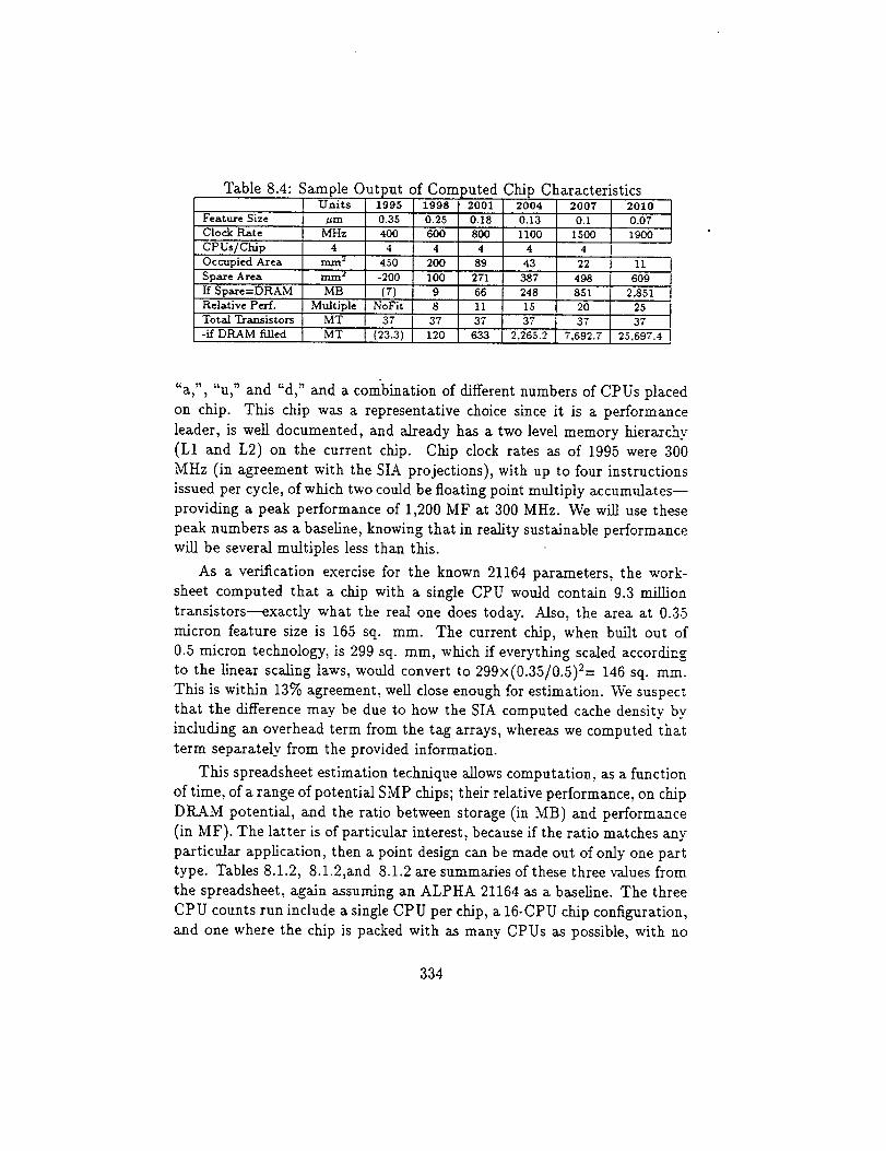
Table 8.4: Sam ltput of Computed Chi CharacteristicsUnits 1995 1998 2001 2004 2007 2010
Feature Size /_m 0.35 0.25 0.18 0.13 0.1 0.07
Clock Bate MHz 400 600 800 1100 1500 1900
CPUs/Chip 4 4 4 4 4 4
Occupied Area m.m s 450 200 89 43 22 11
Spare Area rnJm -_ -200 100 271 387 498 609
If Spaxe=DRAM MB {7} 9 66 248 851 2.851
Relative Perf. Multiple NoFit 8 11 15 20 25
Total Transistors MT 37 37 37 37 37 37
-if DRAM filled MT (23.3) 120 633 2,265.2 7,692.7 25,697.4
"a,", "u," and _d," and a combination of different numbers of CPUs placed
on chip. This chip was a representative choice since it is a performance
leader, is well documented, and already has a two level memory hierarchy
(L1 and L2) on the current chip. Chip clock rates as of 1995 were 300
MHz (in agreement with the SL_ projections), with up to four instructions
issued per cycle, of which two could be floating point multiply accumulates--
providing a peak performance of 1,200 MF at 300 MHz. We will use these
peak numbers as a baseline, knowing that in reality sustainable performance
will be several multiples less than this.
As a verification exercise for the known 21164 parameters, the work-
sheet computed that a chip with a single CPU would contain 9.3 million
transistors---exactly what the real one does today. Also, the area at 0.35
micron feature size is 165 sq. mm. The current chip, when built out of
0.5 micron technology, is 299 sq. ram, which if everything scaled according
to the linear scaling laws, would convert to 299x(0.35/0.5)2= 146 sq. ram.
This is within 13% agreement, well close enough for estimation. We suspect
that the difference may be due to how the SIA computed cache density by
including an overhead term from the tag arrays, whereas we computed that
term separately from the provided information.
This spreadsheet estimation technique allows computation, as a function
of time, of a range of potential SMP chips; their relative performance, on chip
DRAM potential, and the ratio between storage (in MB) and performance(in MF). The latter is of particular interest, because if the ratio matches any
particular application, then a point design can be made out of only one part
type. Tables 8.1.2, 8.1.2,and 8.1.2 are summaries of these three values from
the spreadsheet, again assuming an ALPHA 21164 as a baseline. The three
CPU counts run include a single CPU per chip, a 16-CPU chip configuration,
and one where the chip is packed with as many CPUs as possible, with no
334

Table8.5: PeakPerformancein MF perChipYear Max DRAM: 1 CPU
ASIC _P DSP ASIC _P
1995 1,200 1,200 1,200
1998 1,200 2,400 2,400
2001 1,200 2,400 3,600 19,200 38,400
2004 1,200 3,600 4,800 25,200 51,600
2007 2,400 3,600 6,000 32,400 63,600
2010 2,400 4,800 7,200 39,600 70,800
16 CPUs No DRAM: Max CPUs
DSP ASIC uP DSP
1,200 2,400 3.600
7,200 10,800 14.4OO
51,600 24,000 38,400 51.600
70,800 t 72,000 124,800 171.600
96,000 ] 228,000 384.000 576.000
121,200 I 618,000 994,8OO 1,717,200
extra onboard DRAM. In all cases, we assume that each CPU has its own
96 KB L2, as is present today (it may be reasonable to assume larger L2s).
Note that the technology is not dense enough for 16 CPUs until 2001. Notealso that in Table 8.1.2, the columns for Max CPUs list the number of CPUs
on chip and not the extra DRAM (since there isn't any).
Given these numbers, there is a variety of potential chips that might
make for suitable point design basis. For purposes of discussion we will
assume 2004 technology for a 2007 point design system.
For a single CPU per chip, but stuffed with DRAM, we can get chips
with 1 GF to almost 5 GF of performance, and sufficient DRAM to give
a memory ratio of from 0.06 to 0.47--serious numSers that would allow
construction of a single part type machine of from 20,000 to 100,000 chips.
For a 16-way SMP on chip, peak performance would run from 25 to
70 GF, with perhaps a 100 MB of DRAM for an L3, meaning that a few
thousand CPU chips would be suitable, but with external DRAM a necessity.
At 2 GB per chip, this might require upwards of 50,000 DRAMs for a full
100 TF of memory. Bandwidth for this external memory also needs to be
investigated.
Stuffing a chip with CPUs only, would reduce the total number of CPU
chips to under a thousand, but with no on chip DRAM for L3, and zhus
more bandwidth needed off chip.
In all cases we are talking about a machine with on the order of 50.000
to 100,000 separate CPUs all running concurrently. System software must
be capable of managing this level of parallelism efficiently if any meanin_ul
fraction of the system's peak is to be utilized.
In all cases, power needs to be more carefully estimated to ensure that
the chips have not exceeded maximum thermal limits.
335
Table 8.6: DR_4.M on Chip at Peak Performance (in MB) per ChipYear Max DRAM: 1 CPU 16 CPUs No DRAM: Max CPUs
ASIC uP DSP ASIC uP DSP ASIC uP DSP
1995 I0 5 5 2 2 2
1998 54 23 23 9 6 6
2001 174 82 82 " 42 1 1 20 16 16
2004 563 268 268 372 165 165 45 39 39
2007 1861 878 878 1615 740 740 114 96 96
2010 6527 2890 2890 6130 2698 2698 247 226 226
Table 8.7: Ratio of DRAM to MF per ChipYear Max DRAM: 1 CPU 16 CPUs No DRAM: Max CPUs
ASIC, uP DSP ASIC uP DSP ASIC _P , DSP
I I1995 0.01 0.00 0.00
1998 o.o51o.o,O.Ol2001 0.15 0.03 0.02 0.00 0.00 0.00
2004 0.47 0.07 0.06 0.01 0.00 0.00
2007 0.78 0.24 0.15 0.05 0.01 0.01 I
i2010 2.72 0.60 0.40 0.15 0.04 0.02
336