FINAL REPORT - NASA · FINAL REPORT YEAR-1 Adjustable Focus Optical ... information was published...
32
FINAL REPORT YEAR-1 Adjustable Focus Optical Correction Lens (AFOCL) Contract NAS8-O0118 Submitted July 24, 2001 Prepared by Dr. Bruce R. Peters Center for Applied Optics The University of Alabama in Huntsville Huntsville, Alabama 35899 TEL: 256-824-2526 petersb @ emait, uah.edu https://ntrs.nasa.gov/search.jsp?R=20010072401 2018-07-13T23:49:11+00:00Z
Transcript of FINAL REPORT - NASA · FINAL REPORT YEAR-1 Adjustable Focus Optical ... information was published...
FINAL REPORT
YEAR-1
Adjustable Focus Optical Correction Lens (AFOCL)
Contract NAS8-O0118
Submitted
July 24, 2001
Prepared by
Dr. Bruce R. Peters
Center for Applied Optics
The University of Alabama in HuntsvilleHuntsville, Alabama 35899
TEL: 256-824-2526
petersb @ emait, uah.edu
https://ntrs.nasa.gov/search.jsp?R=20010072401 2018-07-13T23:49:11+00:00Z


Final Report, Year-1 for NAS8-00118
Adjustable Focus Optical Correction Lens (AFOCL)
Prepared by Dr. Bruce R. Peters
Center for Applied Optics
The University of Alabama in Huntsville
Technical Summary:
This report describes the activities and accomplishments along with the status of thecharacterization of a PLZT-based Adjustable Focus Optical Correction Lens (AFOCL) test device. The
activities described in this report were undertaken by members of the Center for Applied Optics (CAd) at
the University of Alabama in Huntsville (UAH) under NASA Contract NAS8-00188. The effort was led byDr. Bruce Peters as the Principal Investigator and supported by Dr. Patrick Reardon, Ms. Deborah Bailey,
and graduate student Mr. Jeremy Wong. The activities outlined for the first year of the contract were to
identify vendors and procure a test device along with performing the initial optical characterization of thetest device. This activity has been successfully executed and test results are available and preliminary
information was published at the SPIE Photonics West Conference in San Jose, January 2001. The
paper, "Preliminary investigation of an active PLZT lens," was well received and generated response withseveral questions from the audience.
A PLZT test device has been commercially procured from an outside vendor: The University of
California in San Diego (UCSD) in partnership with New Interconnect Packaging Technologies (NIPT) Inc.The device has been subjected to several tests to characterize the optical performance of the device at
wavelengths of interest. The goal was to evaluate the AFOCL similar to a conventional lens and measureany optical aberrations present due to the PLZT material as a deviation in the size of the diffraction limited
spot (blur), the presence of diffracted energy into higher orders surrounding the focused spot (a variationin Strehl), and/or a variation or spread in the location of the focused energy away from the optical axis (abias towards optical wedge, spherical, comma, or other higher order aberrations). While data has beencollected indicative of the imaging quality of the AFOCL test device, it was not possible to fully
characterize the optical performance of the AFOCL alone because there were significant opticaldistortions due to fabrication related issues.
The initial device appears to have significant amounts of bias in the lens, even when no voltage is
applied. This is consistent with the imaging data acquired and is likely attributable to the mounting
procedure used by NIPT and UCSD. The substandard quality of the optical mounting and fabrication ofthe device places an overwhelming bias on the measurements making it difficult to separate true optical
performance from poor manufacturing. While issues of optical bonding and attachment of electrodes areall technologies readily available from the electronics industry, NIPT has very limited access to equipment
and processes to improve their fabrication quality. Given the current limited capabilities of UCSD/NIPT, itis doubtful that the quality of their production could be significantly increased without unreasonable
increases in financial backing that is not evident at this time.
Alternative vendors have been identified within the United States (NZ Technologies Inc.) and
several in Europe; but initial contact has not been well received. NZ has positioned itself to be a supplier
of active optic components and Spatial Light Modulators for the high volume production in thecommunications industry and is uninterested in producing special research devices at this time. Likewise,
the variety of European potential suppliers are more university based and as such, their capabilities may
be equally limited as UCSD/NIPT and as such may not be capable of producing a better quality device.
It is suggested that procurement of additional devices to proceed with subsequent years ofresearch and technology demonstration as outlined in the original proposal may be of limited if any value.
The current testing could continue along with additional testing not previously proposed to betterunderstand the performance of the AFOCL and to attempt to extract meaningful data from the aberrated
test device.

Final Report for NAS8o00118
Adjustable Focus Optical Correction Lens (AFOCL)
Introduction:
The need for on-orbit adjustment of an optical system is becoming more imperative as the design
and fabrication of lighter weight, higher wavefront quality, large aperture telescopes continues. Thedecreased weight of the next generation ultra-light very large optics has limited the inherent stiffness of
the optical elements. This increases the probabilities of developing optical surface deformations and
degrading optical system performance. Traditional on-orbit realignment of telescopes typically relies onrefocusing and realignment of selected optical elements (physical translations and rotations). However,
high-resolution space telescopes prefer to limit mechanical displacement of optical elements to minimizeundesired vibrations. A great deal of development is underway to create small robust actuators suitable
for telescope alignment and as actuators in active or deformable mirrors. _ The extreme vacuum of space
places demands on the long-term stability of the materials and lubricants, often requires heaters toprevent freezing of components, and is limited with regards to response time required to achieve a
precise movements. Therefore, nonmechanical approaches to optical correction are being explored.
One approach has been to develop electro-optical devices that can modulate and steer an opticalbeam without relying on physical displacement of the optical components. Several forms of optical
phased arrays have been proposed that utilize a variety of electro-optical materials to impose amodulation of the optical phase front to achieve deflection, focussing, and aberration correction. 2 Such
devices affect the phase front of the optical beam in a way that is similar to the way diffractive optical
elements, holographic optical elements, anamorphic high-order lenses, and spatial light modulators
(SLM) can affect the phase front. In so doing, they are able to impose a particuliar desirable phase profileonto an incident beam and thereby improve optical quality of the beam. Typically, the optical system ismodeled and the aberrations are calculated or measured and wavefront correcting optics are introduced
into the optical path to essentially reverse or minimize the degredation in the optical quality. While the
magnitude of the phase front manipulation is more limited with electro-optical devices compared withconventional transmissive optics, the versatility of the electro-optical devices permits them to perform
dynamic phase manipulation within carefully defined limits. In this fashion, the electro-optical approachescan provide potentially greater flexibility to the optical designer since the devices are capable of correctinga larger range of aberrations and adapting to a larger range of wavefront errors. The adaptability ofelecto-optical devices is what makes them so attractive. Liquid-crystal, 3'4 LiNbO3 crystal, s along withPLZTel°have all been demonstrated as candidates for application to dynamic devices. Typically, a
change in voltage applied to the device or to subapertures or pixels within the device will produce anelectro-optic effect that that perturbs the optical property of the material that then modifies the transmitted
phase front. One material in particuliar, polycrystalline lead lanthanum-modified zirconate titanate (PLZT)is attractive because the material demonstrates a strong quadratic electro-optic effect at moderate
voltages. The electro-optic coefficient of PLZT is typically larger than other candidate materials and the
material is typically less expensive and easier to handle. When compared to liquid crystal, PLZT can havea faster response time and can more readily be integrated into the electronic circuits.
PLZT-based electro-optical devices have been demonstrated for many applications including
tunable gratings, optical switches, dynamic lenses, high-speed shutters, and scanning devices. Because
of the scattering properties of the material and the strength of the electrical field required to produce asubstantial phase modulation, the PLZT devices are typically made very thin and use surface electrodes.However, the solid-state nature of the PLZT makes it ideal for integration with conventional electronic
circuits and thereby reduce the complexity of the device with regards to the number of externalconnections and controls. In fact, the integration of voltage controlling resistors and support circuitry has
been demonstrated for a PLZT beam-steering device with only two external electrical connections
required. 1_ This paper describes a similar application of PLZT to fabricate an adjustable focus opticalcorrection lens (AFOCL) to perform variable focusing and integrated wavefront correction. The purpose is
to create a system that achieves stable alignment under a variety of environments and over time by
incorporating a dynamic realignment with phase front correction capability rather than adjusting the muchmore massive solid refractive lenses often used in optical imaging systems such as telescopes and other
optical sensors.
2


Final Report for NAS8-00118
Adjustable Focus Optical Correction Lens (AFOCL)
Ferroelectric ceramic based Spatial Light Modulators (SLMs) have been investigate for such
applications, 1215 but high-voltage requirement and large-field induced effects near the half-wave voltagehave prohibited their utilization. Thinned ferroelectric materials can lower the voltage requirement and
stacking or cascading several devices within the optical train can avoid large-field induced effects. TheAFOCL works in transmission rather than reflection maintaining the compactness of the optical system.
Differing from liquid crystal display (LCD) based devices that can have intrinsically large wavefrontaberrations of their own due to the nature of their construction, the PLZT material is solid which permits it
to be optically polished to minimize wavefront aberrations. Furthermore, the material could be polishedinto lens-like shapes to further broaden its potential through the creation of hybrid active and refractive
optical elements. The application of the material beyond the visible region of the infrared spectrum hasbeen limited. Therefore, the activity proposed here emphasized the extension of PLZT-based devices into
the infrared.
References:
1. R.K. Tyson, Principles of Adaptive Optics, Academic Press, Boston, MA (1997).
2. G. Haertling, "Electro-optic ceramics and devices," Electronic Ceramics: Properties, Devices and
Applications, Marcel Dekker, New York, NY, 371-492 (1998).
3. T.J. Chen, P.J. Bos, H. Vithana, and D. L. Johnson, "An electro-optically controlled liquid crystal
diffraction grating," Applied Physics Letters, 67, 2588-2590 (1995).
4. N.A. Riza and M.C. DeJule, =Three terminal adaptive nematic liquid-crystal lens device," Optics
Letters, 19, 1013-1015 (1994).
R.T. Chen, D. Robinson, H. Lu, M.R. Wang, T. Jannson, and R. Baumbick, "Reconfigurable opticalinterconnection network for multimode optical fiber sensor arrays," Optical Engineering, 31, 1098-
1106 (1992).
Q. Wang Song, X.M. Wang, and R. Bussjager, "PLZT ceramic wafer-based electro-optic dynamic
diverging lens," Optics Letters, 21,242-244 (1996).
Q.W. Song, P.J. Talbot, and J.H. Maurice, "PLZT based high-efficiency electro-optic grating for
optical switching," Journal Modern Optics, 41, 717-727 (1994).
T. Tatebayashi, T. Yamamoto, and H. Sato "Electro-optic variable focal-length lens using PLZT
ceramic," Applied Optics, 30, 5049-5055 (1991).
9. J.A. Thomas, M. Lasher, Y. Fainman, and P. Soltan, "A PLZT-based dynamic diffractive optical
element for high speed, random-access beam steering," Proc. SPIE Vol. 3131, 124-132 (1997).
10. K. Nagata, "PLZT optical shutter with copper electrodes by electroless plating," Ferroelectrics, 109,
247-252 (1990).
11. Q. Wang Song, X.M. Wang, R. Bussjager, and J. Osman, "Electro-optic beam-steering device basedon lanthum-modified lead zirconate titanate ceramic wafer," Applied Optics, 35, 3155-3162 (1996).
12. G.D. Love, J.V. Major, and A. Purvis, "Liquid-crystal prisms for tip-tilt adaptive optics," Optics Letters,
19, 1170-1172 (1994).
13. V.A. Berenberg, A.A. Leshchev, M.V. Vasirev, V.Y. Venediktov, A.P. Onokhov, and L.A. Beresnev,
"Dynamic correction for distortions in imaging optical systems using liquid crystal SLMs," Proc. SPIE,Vol. 3432, 110-119 (1998).
14. Raimo Silvennoinen, Kai-Erik Peiponen, Andris Krumins and Jari R&s&nen, Optical quality inspection
of PLZT ceramics by using CGH-element, Optical Materials, 7, 145-152, 1997.
15. Bryknar Z., Bykov I., Dimza V., Jastrabik L., Savinov A., Soukup L., Trepakov V.: Optical Spectra ofPLZT Ceramics. In: Electroceramics IV. Proc. of the 4th Int. Conf. on Electronic Ceramics and
Applications., 431-434, 1994.
,
,
.
.
3

Final Report for NAS8-00118
Adjustable Focus Optical Correction Lens (AFOCL)
Activities:
UAH began the optical design and specification of the first Adjustable Focus Optical Correction
Lens (AFOCL) during the summer of 1999 and finalized it by August. The design was strongly influenced
by the capabilities of the fabricators: New Interconnect Packaging Technologies, (NIPT) and theUniversity of California San Diego (UCSD). The eventual specifications to be given to NIPT and UCSDwere discussed at a technical interchange meeting (TIM), Monday May 22, 2000 at NIPT in San Diego,
California. The meeting involved Billy Lightsey from NASA-Space Optics and Manufacturing Center
(SOMTC) at Marshall Space Flight Center in Huntsville, along with Dr. Bruce Peters and Dr. PatrickReardon from the CAO. The AFOCL performance goals were outlined and technical objectives were
discussed. NIPT provided their proposal for the PLZT active lens. During the subsequent discussion,UAH was able to provide clarification to NIPT regarding the performance goals that resulted in therelaxation of some fabrication specifications that will enable acceptable performance while minimizing
technical risk.
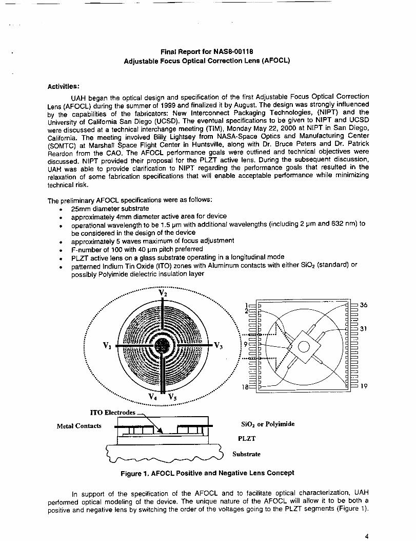
The preliminary AFOCL specifications were as follows:• 25ram diameter substrate
• approximately 4mm diameter active area for device
• operational wavelength to be 1.5 pm with additional wavelengths (including 2 pm and 632 nm) to
be considered in the design of the device
• approximately 5 waves maximum of focus adjustment
• F-number of 100 with 40 pm pitch preferred
• PLZT active lens on a glass substrate operating in a longitudinal mode
• patterned Indium Tin Oxide (ITO) zones with Aluminum contacts with either SiO2 (standard) or
possibly Polyimide dielectric insulation layer
°°°°°.°°.°°°°°°°°°° ............. V2 ............ .°°°°°°o
.'*" "'" "*'-.....% 12 36• V] 31
,,•... ...- 19
"" ....... V4 V5 .........""
ITO Electrodes _._
Metal Contacts Si02 or Polyimide
PLZT
Substrate
Figure 1. AFOCL Positive and Negative Lens Concept
In support of the specification of the AFOCL and to facilitate optical characterization, UAH
performed optical modeling of the device. The unique nature of the AFOCL will allow it to be both a
positive and negative lens by switching the order of the voltages going to the PLZT segments (Figure 1)


Final Report for NAS8-00118
Adjustable Focus Optical Correction Lens (AFOCL)
This means that the AFOCL could be tested in two different configurations and the performance
characterized for both.
The AFOCL is solid state in that the refocusing and wavefront correction is accomplished through
variations in the voltage applied to a thinned and stacked PLZT device instead of mechanically translating
the optic. By varying the voltage to the crystal material, the optical behavior is altered. If the material islaid down into patterns or arrays, using conventional microlithographic fabrication procedures in use by
the semiconductor industry, then the individual pixels can be modulated as required to create almost any
arbitrary phase front desired. Concentric rings can be activated to create focussing lenses or strips canbe modulated to tip and tilt the transmitted light to realign the optical path. Through a stacking or
cascading of the devices, each one performing a specialized wavefront correction, virtually all opticalaberrations within the system could be compensated for and eliminated from the optical train thereby
leading to diffraction limited performance. In this way, larger optics could be made to less demanding
wavefront qualities requirements to keep costs in check and the stacked series of AFOCL elements couldbe used to correct the optical alignment and improve the wavefront quality by "inverting" the aberrationsto back-out errors and enhance optical performance. This is vital to having autonomously operating
space-based telescopes because the sensor will need to be capable of correcting aberrations that will bechanging over time (such as thermal induced defocus, mechanical stress induced aberrations on mirrors,and vibration/thermal misalignment of optical components) to maintain diffraction limited system
performance.
An analysis was performed to determine the optimal design specifications for the AFOCL
adaptive optic. The analysis evaluated the tradeoffs between the form of the phase function, themagnitude of the phase induced across the optic, and the structure of the annular pixels. The pixels couldbe of identical width, or the pixels could vary with distance from the center of the optic. These tradeoffswere measured by how they affected diffraction efficiency, manufacturability, and functionality of thedevice. It was determined that, for achieving the desired functionality for the device, the most appropriate
pattern would be a quadratic phase function which, depending on the sign of the phase change, would
yield a positive or negative lens. Since this device was to have annular "pixels," the approach to thedesign was analogous to a stepped-approximation to a phase grating. Thus, each ring would generate
specific phase lags such that main diffracted order for the system would yield the desired lensing power.The next question to answer was how much power, and how many steps for each 2Tr of phase.
The efficiency of the I st diffracted order given a stepped approximation to a properly blazed
grating can be computed using the following equation:
where s is the number of steps. Evaluating discrete values for s yields the following results:
Steps (s) Diffraction
Efficiency41%
Improvement
in Efficiency
95%
2
3 68% 41%
4 81% 16%
5 88% 7%
6 91% 4%
7 93% 2%
2%
5


Final Report for NAS8-00118
Adjustable Focus Optical Correction Lens (AFOCL)
By increasing the number of levels in the stepped approximation, the diffraction efficiency clearlyincreases, however, the percentage of improvement in the efficiency in going from N to N+I steps isincreasingly smaller as N increases. This predicted performance is analogous to the performance of anystep-wise approximation to a pure phase function similair to diffractive and binary optical elements. Thus,from this analysis, we selected a 5-step approximation as it has sufficient efficiency and, as will be shown,it further simplified manufacturing.
Since the number of steps has been selected, we can now determine how much quadratic phaseour device should generate. The device produces phase of the form E](r) = Ar2 where r is the radialdistance from the center of the device. The gradient of the phase is given by _E](r) = 2Ar, and theminimum feature size can be calculated using the equation
MFS -7_(r,_). s
2
2 A r,._, . s
l OA r._
where rmax is the semidiameter of the device and _ is the wavelength of operation, 2.0518micrometers. Thus, the larger diameter the element and the greater the magnitude of the phase, thesmaller the minimum feature size will be. Based on vendor recommendations and in order to mitigateproduction related risks, it was decided that a diameter of 4mm and a total phase of 5 waves, A =1.25Mmm 2, was appropriate. This yields a minimum feature size of approximately 40 I_mthat is well withinthe tolerances of the fabrication process and also considered to be very low risk.
The complete quadratic phase function of the device is achieved by setting every 5th ring to equaland specific voltages in such a way that the rings produce optical path delays of 0, M5, 2 _k/5, 3 k/5, and4A/5. By starting with the central disk at 0 phase, and increasing the optical phase delay on the rings as rincreases, a negative lens is generated. If, however, one was to start the central disk at I and thendecrease the optical phase delay on the subsequent rings, one would have a positive lens. Fortunately,for a diffractive lens such as this, a delay of 0 _ is identical to a delay of 1 _k,thus, the identical delays(voltages) need only be rearranged to switch between a positive and a negative lens. These results areshown graphically in Figure 2.
While the electrodes in a conventional approach are typically fabricated using opticallytransparent indium tin oxide (ITO), the power feeds in this device were going to be aluminum instead ofITO. Therefore, the opaque conductive lines would partially obscure and diffract some of the light. Theeffects of this on the throughput of the device can be readily calculated. The effects can be described intwo ways. First, the lines produce a reduction in the transmitting area. Since there are 5 conductivelines, and each line is 0.040mm wide and 2mm long, they provide 0.4mm 2 of obscuration. Compared tothe full 4mm diameter aperture, the conductive lines reduce the overall throughput of the device by 3%.
The second effect the conductive lines produce is a change in the diffraction pattern relative to anunobscured circular aperture. The pattern for the unobscured aperture is simply the Airy disk pattern(Figure 3a). The conductive lines, however, add some additional structure to the pattern. The linesconsist of three parallel but displaced lines, and two parallel lines perpendicular to the other three. Ascan be seen in the first two plots of the point spread function, the diffraction from the conductive lines is,on a linear scale, imperceptible. Even when plotted on a log scale, the effects are negligible, thoughnoticeable (Figure 3b).


Final Report for NAS8-00118
Adjustable Focus Optical Correction Lens (AFOCL)
And) 2(p)
Bind) 2(p)
0.0021
0.001
I
._]
1
o
i
/!
...-o
1.5
II °'
t_ I
i_ I
.+ j J !
i i, .
J I ....; i
: l : 1
2
And) 2(p)
Bind) 2 (p)
0.0021
0.001
00 0.5 I
I)
I
\
iii
i ! i
1.5
Figure 2. AFOCL Positive and Negative Lens Test Configurations
! 11
(a) (b)Figure 3. Modeled AFOCL Transmission
7


Final Report for NAS8-00118
Adjustable Focus Optical Correction Lens (AFOCL)
In preparation for delivery and testing of the AFOCL device, UAH has designed the optical
system (Figure 4). The lenses, optical mounts, and other fixtures were identified and orders were placed
to procure the necessary testing hardware. A commercially available positive lens and negative lens wereidentified to serve as an AFOCL emulator to facilitate alignment prior to the delivery of the actual AFOCLfrom NIPT. The emulator will permit development and characterization of the optical test set-up, serve as
a known reference source for calibration of the test data, and provide a comparison to the actual AFOCL
performance.
AFOCL Image Plane
59.600 mm
76.569 mm
Figure 4. AFOCL Positive and Negative Lens Test Configurations
Figure 5. AFOCL Photolithographic Mask
Dr. Peters visited NIPT on Tuesday, August 1, 2000 to discuss the mask generation process and
to review the proposed design. Following the successful review, the design was translated into e-beamdata files to write the mask pattern. Figure 5 shows the completed masks. The fabrication specifications
were finalized by August and the photolithographic masks were designed and procured. NIPT completed
generating e-beam data for the photolithographic masks. UAH reviewed the design and in collaborationwith NIPT, the electrode pattern design was revised from the first iteration radial pattern to one that
consists of only horizontal or vertical lines to reduce the cost of the design and e-beam writing.
The test device was delivered in October with the initial checkout of the device in November to
verify connectivity and continuity of the AFOCL wire bonds. The initial performance is shown optically in
Figure 6. The images are taken using a CCD camera. There is no voltage to the device in Figure 6 (a)with all of the electrodes effectively connected to ground. The expanded speckled HeNe laser is passed
through the 4 mm diameter aperture of the device and the resulting intensity pattern is shown (within


Final Report for NAS8-00118
Adjustable Focus Optical Correction Lens (AFOCL)
larger circle). Then, three of the ring electrodes or zones are connected to the ground and the remainingtwo rings to 280V, and illuminated by the laser. The device is operating as a very poor diffrative optic
collecting lens (smaller circle) because the voltage is way off of the designed voltage; yet, the devicedoes focus some of the light. Testing then began in earnest in November using the UAH designed voltage
supply circuit (Figure 7).
(a) (b)
Figure 6. AFOCL Transmission Demonstration
Figure 7. High Voltage Power Supply and Regulation Circuit
Testing and Characterization:
The areas to be investigated include intensiomentric effects (those that limit or alter the intensity
of the light transmitted through the optic); interferometric effects (the phase change induced through the
optic); and polarimetric effects (evaluating the differential lag between two polarization states propagating
through the optic). These distinct phenomena are often coupled together in real applicationsconsequently, there is a need to develop different standardized testing apparatus to: (1) isolate one effectfrom another; (2) gather information for understanding the physical effects; (3) anchor wavefront corrector
modeling efforts; (4) develop the ability to decouple different effects; (5) demonstrate the suitability of
PLZ'r technology to perform wavefront correction.
The CAO had at its disposal, traditional interferometers available within the CAO Optical
Metrology Laboratory and the Advanced Polarization Test Facility. Besides the imaging andinterferometers available, the polarimetry facility has at its disposal, a Mueller Matrix Imaging Polarimeter
(MMIP) which is well suited to the characterization of SLMs, polarizers, and thin film coatings within thevisible and near-IR spectrums. In addition, the phase-shifting interferometry facilities at NASA-MSFC and

Final Report for NAS8-00118
Adjustable Focus Optical Correction Lens (AFOCL)
the unique interferometers they processes are some of the most advanced available and may be of valueespecially for performing real-time optical performance evaluation of AFOCL test components.
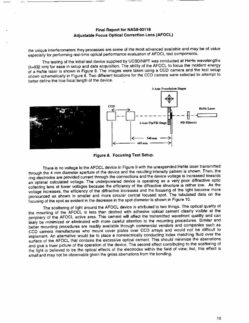
The testing of the initial test device supplied by UCSD/NIPT was conducted at Helle wavelengths(_k=632nm) for ease in setup and data acquisition. The ability of the AFOCL to focus the incident energyof a HeNe laser is shown in Figure 9. The images were taken using a CCD camera and the test setupshown schematically in Figure 8. Two different locations for the CCD camera were selected to attempt tobetter define the true focal length of the device.
3-A_ds Translation Stages
ccv [ _
=...°=_t e. ==t_...,.
%..... .: . ..... .:
645 mm >
'1...... []- -!
ND Filter(s)
HeNe Laser
Figure 8. Focusing Test Setup.
There is no voltage to the AFOCL device in Figure 9 with the unexpanded HeNe laser transmittedthrough the 4 mm diameter aperture of the device and the resulting intensity pattern is shown. Then, thering electrodes are provided current through the connections and the device voltage is increased towardsan optimal calculated vottage. The underpowered device is operating as a very poor diffractive opticcollecting lens at lower voltages because the efficiency of the diffractive structure is rather low. As thevoltage increases, the efficiency of the diffractive increases and the focusing of the light become morepronounced as shown in smaller and more circular central focused spot. The tabulated data on thefocusing of the spot as evident in the decrease in the spot diameter is shown in Figure 10.
The scattering of light around the AFOCL device is attributed to two things. The optical quality ofthe mounting of the AFOCL is less than desired with adhesive optical cement clearly visible at theperiphery of the AFOCL active area. This cement will affect the transmitted wavefront quality and canlikely be minimized or eliminated with more careful attention to the mounting procedures. Similar andbetter mounting procedures are readily available through commercial vendors and companies such asCCD camera manufactures who mount cover plates over CCD arrays and would not be difficult toimplement. An alternative would be to place a nonelectrically conducting index matching fluid over thesurface of the AFOCL that contains the excessive optical cement. This should minimize the aberrationsand give a truer picture of the operation of the device. The second effect contributing to the scattering ofthe light is believed to be the optical effects of the electrodes within the field of view; but, this effect issmall and may not be observable given the gross aberrations from the bonding.
10


Final Report for NAS8-00118
Adjustable Focus Optical Correction Lens (AFOCL)
Unexpanded HeNe Beam
540 mm distance from AFOCL
0 Volts 100 V
645 mm distance from AFOCL
200 V 280 V
0 Volts 100 V 200 V
Figure 9. Focusing Images.
250 V
0 Volts 280 Volts Reduction
Diameter 6.10 3.81 37.50 %
Area 29.22 11.40 60.99 %
0 Volts 250 Volts Reduction
Diameter 7.37 42.66 37.07%
Area 5.08 20.27 52.49%
Figure 10. Tabulated Data from Initial Checkout Test.
Interferometric Testing:
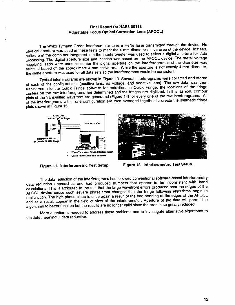
The testing of the AFOCL is emphasizing the interferometric measurements of the AFOCL
device. The device was placed in the test setup as shown in Figure 11 and 12. The test is a double pass
interferogram of the AFOCL with three different operational states: positive lens, voltage off, and negative
lens. The maximum voltage for both the positive and negative lens configurations was 250 Volts.
11

FinalReportfor NAS8-00118AdjustableFocusOpticalCorrectionLens(AFOCL)
The Wyko Tymann-Green Interferometer uses a HeNe laser transmitted through the device. No
physical aperture was used in these tests to mark the 4 mm diameter active area of the device. Instead,software in the computer integrated into the interferometer was used to select a digital aperture for data
processing. The digital aperture size and location was based on the AFOCL device. The metal voltagesupplying leads were used to center the digital aperture on the interferogram and the diameter wasselected based on the approximate 4 mm active area. While the aperture is not exactly 4 mm diameter,the same aperture was used for all data sets so the interferograms would be consistent.
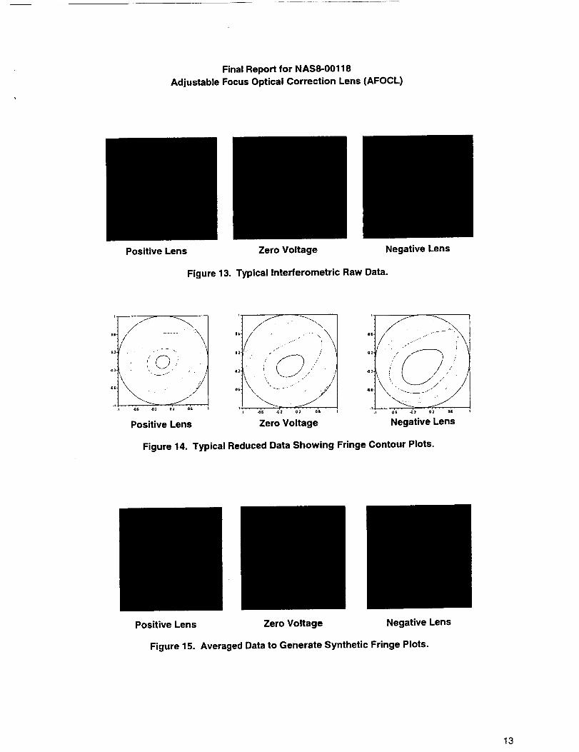
Typical interferograms are shown in Figure 13. Several interferograms were collected and stored
at each of the configurations (positive lens, no voltage, and negative lens). The raw data was thentransferred into the Quick Fringe software for reduction. In Quick Fringe, the locations of the fringecenters on the raw interferograms are determined and the fringes are digitized. In this fashion, contour
plots of the transmitted wavefront are generated (Figure 14) for every one of the raw interferograms. All
of the interferograms within one configuration are then averaged together to create the synthetic fringeplots shown in Figure 15.
AFOCL on
2-Axis Tip/Tilt Stage
I Interferomete_
__..oron 2-Axis Tlw'rJlt Stage
• Wyko Twymann-Green IntQrferometer
• Quick Fringe Anllysls Software
Figure 11. Interferometric Test Setup. Figure 12. Interferometric Test Setup.
The data reduction of the interferograms has followed conventional software-based interferometry
data reduction approaches and has produced numbers that appear to be inconsistent with handcalculations. This is attributed to the fact that the large wavefront errors produced near the edges of theAFOCL device cause such severe phase front changes that the fringe following algorithms begin to
malfunction. The high phase slope is once again a result of the bad bonding at the edges of the AFOCLand as a result appear in the field of view of the interferometer. Aperture of the data will permit the
algorithms to better function but the results are no longer valid since the area is so greatly reduced.
More attention is needed to address these problems and to investigate alternative algorithms tofacilitate meaningful data reduction.
12

Final Report for NAS8-00118
Adjustable Focus Optical Correction Lens (AFOCL)
Positive Lens Zero Voltage Negative Lens
Figure 13. Typical Interferometric Raw Data.
Positive Lens
O6
021
1
-I
. ....-.\ \_
../ _/. ¸'" ,_
Zero Voltage
1
_2
\\ --..........." //
Negative Lens
Figure 14. Typical Reduced Data Showing Fringe Contour Plots.
Positive Lens Zero Voltage Negative Lens
Figure 15. Averaged Data to Generate Synthetic Fringe Plots.
13


FinalReportfor NAS8-00118AdjustableFocusOpticalCorrectionLens(AFOCL)
Conclusions:TheCAOhasdemonstratedthatthePLZTbasedtechnologyis capableof producinga variable
oradjustablefocuslens.A vendorwasidentified,a testdevicewasdesignedandprocured,and initialtestingperformed. As expected, the optical power is greater in the positive lens configuration than the
negative lens configuration. However, there appears to be significant amounts of bias in the lens to beginwith, even when no voltage is applied. This is consistent with the imaging data acquired and is likelyattributable to the mounting procedure used by NIPT and UCSD. The substandard quality of the optical
mounting and fabrication of the device places an overwhelming bias on the measurements making itdifficult to separate performance from poor manufacturing. While issues of optical bonding andattachment of electrodes are all technologies readily available from the electronics industry, NIPT has
very limited access to equipment and processes to improve their processes. Given the current limitedcapabilities of UCSD/NIPT, it is doubtful that the quality of their production could be significantlyincreased without unreasonable increases in financial backing that is not evident at this time.
Proposed Plan of Action:
• Continue with the testing of the existing device, especially advanced interferometry to better
characterize the performance of the device in spite of the strong bias from the poor
production processes. This needs to include investigation of data reduction algorithms thatcan function over apertures containing severe phase changes due to the localized bad areas
attributed to bonding quality.
• Expand the optical testing to investigate polarization effects and optical material effects andinvestigate whether using the Mueller Matrix Imaging Polarimeter will yield any meaningful
results given the large biases and aberrations present in the current device.
• Investigate image quality measurements using the Nodal Slide experimental apparatus
possessed by the CAO.
• Delay procurement of another device until either: (1) NIPT demonstrates greater capability inbonding processes; (2) an alternative vendor can be identified.
14

REPORT DOCUMENTATION PAGE Fonw A/_orovedOMB No. 0704.0188
lul=jact I_ my !Umllly _ur _ Io_ vv_la _ of Inlurn/lun R Icdum _ _ mmcu'_ v_ _ c'mlU ,'inu.tl_'.
PI..IEAE 00 NOT I:IETUI_I YOUR FORM TO THE ABOVE AJ[)J_qESS.
i 1. FUEPORTDATE (DO-MM-YYYY/ 2. REPORT TYPE 3. DATES COVERED (From - To)
7/24/01 FINAL4. TITLE AND SUBTITLE
Adjustable Focus Optical(AFOCL)
6. AUTHOfliS)
Dr. Bruce Peters
Correction Lens
5110100--519101_. CO_RACT NUMBER
NAS8-O01186b. GRANT NUMBER
•.'_. PROGRAM ELEME:NT NUMBER
5e. TASK NUMBER
5f. WORK UNIT NUMBER
7. PERFORMING ORGANIZATION NAME(S} AND ADDRESSES)
UAH
Huntsville, AL 35899
9. SPONSORINO/EW)NITORING AGENCY NAME, S) AND ADOfl_)
8. PERFORMING ORGANIZATIONFlIP.PORTNUMB_
910. SPONSOR�MONITOR'S ACRONYM(S)
11. SPONSOR/MONITOR'S RE_DRTNUMWER(S)
12. OIS'T'RIBUTIONIAVAJLABILITY STATEMENT
13. SUPPLEMENTARY NOTES
14. A_'TRACT
15. SUBJECT TERMS
16. SECURITY OULSSIFICATION OF: 17. LIMITATION OF
J;. REPORT b. ABSTRACT e_ THIS PAGE ABSTRACT
IlL NUMBER lga, NAME OF RESPONSIBLE PERSONOFPAGES
19b. TELEPHONE NUMBER r_m cooeJ
Standard Form 2,98 (Rev. 8.,'9B)I'm=t.xll_'O 0V AN._ 3Z_ Z3B, 18