Final Exam, ECE 137A Wednesday March 20, 2019, …...1 a Final Exam, ECE 137A Wednesday March 20,...
33
1 a Final Exam, ECE 137A Wednesday March 20, 2019, Noon - 3 p.m. Name: __________________________ Closed Book Exam: Class Crib-Sheet and 2 pages (4 surfaces) of student notes permitted Do not open this exam until instructed to do so. Use any and all reasonable approximations (5% accuracy), after stating & justifying them. Show your work: Full credit will not be given for correct answers if supporting work is missing. Good luck Time function LaPlace Transform ) (t impulse 1 ) (t U unit step-function s / 1 ) (t U e t 1 1/ 1 / s s ) ( ) cos( t U t e d t 2 2 ) ( d s s ) ( ) sin( t U t e d t 2 2 ) ( d d s Part Points Received Points Possible Part Points Received Points Possible 1a 6 2c 15 1b 5 2d 10 1c 4 3a 7 1d 10 3b 8 1e 10 3c 7 2a 10 3d 8 2b 10 total 100
Transcript of Final Exam, ECE 137A Wednesday March 20, 2019, …...1 a Final Exam, ECE 137A Wednesday March 20,...

1 a
Final Exam, ECE 137A
Wednesday March 20, 2019, Noon - 3 p.m.
Name: __________________________
Closed Book Exam:
Class Crib-Sheet and 2 pages (4 surfaces) of student notes permitted
Do not open this exam until instructed to do so. Use any and all reasonable
approximations (5% accuracy), after stating & justifying them.
Show your work:
Full credit will not be given for correct answers if supporting work is missing.
Good luck
Time function LaPlace Transform
)(t impulse 1
)(tU unit step-function s/1
)(tUe t 1 1/
1 /s s
)()cos( tUte d
t 22)( ds
s
)()sin( tUte d
t 22)( d
d
s
Part Points
Received
Points
Possible
Part Points
Received
Points
Possible
1a 6 2c 15
1b 5 2d 10
1c 4 3a 7
1d 10 3b 8
1e 10 3c 7
2a 10 3d 8
2b 10
total 100
2 a
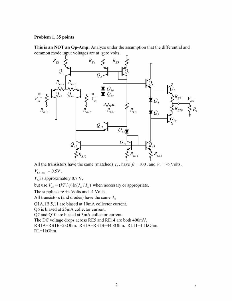
Problem 1, 35 points
This is an NOT an Op-Amp: Analyze under the assumption that the differential and
common mode input voltages are at zero volts
All the transistors have the same (matched) SI , have 100 , and Volts AV .
V5.0)( satCEV .
beV is approximately 0.7 V,
but use )/ln()/( SEbe IIqkTV when necessary or appropriate.
The supplies are +4 Volts and -4 Volts.
All transistors (and diodes) have the same SI
Q1A,1B,5,11 are biased at 10mA collector current.
Q6 is biased at 25mA collector current.
Q7 and Q10 are biased at 3mA collector current.
The DC voltage drops across RE5 and RE14 are both 400mV.
RB1A=RB1B=2kOhm. RE1A=RE1B=44.8Ohm. RL11=1.1kOhm.
RL=1kOhm.

3 a
Part a, 6 points
DC bias---to simplify ,assume for the DC analysis only.
Find the value of the following resistors:
Re5=_____________ Re14=_____________ Re4=_____________
Re15=_____________ Re12=_____________ Re3=_____________
Re7=_____________ Re10=_____________

4 a

5 a
Part b, 5 points
DC bias---to simplify ,assume for the DC analysis only.
On the circuit diagram above, label the DC voltages at ALL nodes, and the DC collector
currents of all transistors. Label the values of all resistors (except RC5).

6 a

7 a
Part c, 4 points
find the following
device Q1AB 11 12 4 6 15 7 10
gm,
mS

8 a
Part d, 10 points.
Find the following, using the actual value of , i.e. =100
Voltage Gain Input impedance
Q1AB
Q11
Q6
Q7
Overall differential
Vout/Vin
Note: with some insight, you can find the combined gain of Q1AB/11 in a single step. If
would would like to do so, omit the separate answers for Q1AB and Q11 in the table
above, and instead fill in the table below,
Voltage Gain Input impedance
Q1AB/ Q11 combination.

9 a

10 a

11 a

12 a
Part e, 10 points
Maximum peak-peak output voltage (show all your work)
For this, you must use the full circuit diagram, not the half circuit diagram.
magnitude and sign of
maximum output signal
swing due to cutoff
magnitude and sign of
maximum output signal
swing due to saturation
Transistor Q7
Transistor Q10
Transistor Q6
Transistor Q15
Transistor Q4
Transistor Q11
Transistor Q1A
Transistor Q1B
Be warned: In some cases a limit is not relevant at all. Mark those answers "not relevant".
But, give a 1-sentence statement below as to why it is not relevant. Q7/10 form a push
pull stage, so be careful about your answer there. .

13 a

14 a

15 a
Problem 2, 35 points
This is an Op-Amp---analyze the bias under the assumption that DC output voltage is
zero volts, that the positive input Vi+ is zero volts, and that we must determine the DC
value of the negative input voltage (Vi- ) necessary to obtain this.
The NMOSFETs have 2/ 2 0.55mA/V ( /1 m)gs g g gK c W L W
0.69mA/V ( /1 m)v gs inj g gK c v W W , / 0.625Vinj gV v L , thV 0.25V,
/1 20V
The PMOS have identical parameters, except, of course, thV is negative.
DDV = +1 V, SSV = -1 V, RL=50 kOhm
All transistors have |Vgs|=0.35V, except for M7 and M15, which have |Vgs|=0.45V, and
except for M8,9,10,11, which have |Vgs|=0.30V
M12,13 are biased at DI =25 A.
M5,7,15 are biased at DI =50 A.
M8,9,10,11 are biased at DI =50 A.

16 a
Part a, 10 points
DC bias.
Analyze the bias under the assumption that DC output voltage is zero volts, that the
positive input Vi+ is zero volts, and that we must determine the DC value of the negative
input voltage (Vi- ) necessary to obtain this.
(Hint, this should give Vi- = 0V)
Find the following:
Gate widths of M12 and M13 = _____________________
Gate width of M7 =_____________________
Gate width of M8 =_____________________
Gate width of M9 =_____________________

17 a

18 a
Part b, 10 points
DC bias
On the circuit diagram above, label the DC voltages at ALL nodes, the drain currents of
ALL transistors, and the gate widths of ALL transistors

19 a

20 a
Part c, 15 points.
You will now compute the op-amp differential gain. Find the following
Voltage Gain Input impedance
Transistor combination
M1,2,13, 13
M5,6 combination
Q9 or Q12.
Q8 or Q15
Overall differential
Vout/Vin
Notes:
1) You can analye M5 and M6 as separate stages, or as a combined stage using
Norton/Thevenin methods. Don’t ask for hints as to how to do this.
2) For M8/9and for M10/11, you can assume that M8 and M9 are on for the positive
signal swing and M10 and M11 are on for the negative signal swing. More accurately,
you can assume, for the signal swing near zero volts, that all are on. If you take the latter
approach (and do it correctly), you will receive a couple of extra credit points. One hint
(don’t ask for any other hints): use symmetry.

21 a

22 a

23 a

24 a

25 a
Part d, 10 points
Maximum peak-peak output voltage at the positive output Vo+ (show all your work)
magnitude and sign of
maximum output signal
swing due to cutoff
magnitude and sign of
maximum output signal
swing due to:
knee voltage (saturation)
Transistor M9
Transistor M11
Transistor M8
Transistor M10
Transistor M4
Transistor M19
Transistor M6
Transistor M14
Be warned: in some cases a limit is not relevant. Mark those answers "not relevant".

26 a

27 a

28 a
Problem 3, 30 points
You will be working on the circuit
to the left
Ignore DC bias analysis. You don’t
need it.
The transistor has transconductance
gm.
Its output resistance Rds is
infinity...so you don't need to
include this element in the circuit
diagram !
Part a, 7 points
Draw a small-signal equivalent circuit of the circuit.

29 a
Part b, 8 points
gm=10 mS. C=1pF. R= 1000 Ohms
Find, by nodal analysis, a small-signal expression for Vout/Vin. Be sure to give the
answer with **correct units** and in ratio-of-polynomials form, i.e.
...1
...1)(
)(
)( e)appropriat (asor
...1
...1
)(
)(2
21
2
21
2
21
2
21
sasa
sbsbsK
sV
sV
sasa
sbsbK
sV
sV n
gen
out
gen
out
Note that an expression like
correctlly dimensiona is )seconds103(1
1 lly wrong;dimensiona is
)103(1
1
)(
)(66 sssV
sV
gen
out
Vout(s)/Vin(s)= __________________

30 a

31 a
Part c, 7 points
Find any/all pole and zero frequencies of the transfer function, in Hz:
_____________,_____________,_____________,_____________
Draw a clean Bode Plot of Vout/Vin,
LABEL AXES, LABEL all relevant gains and pole or zero frequencies, Label Slopes
B

32 a

33 a
Part d, 8 points
Vin(t) is a 0.1 V amplitude step-function.
Find Vout(t)=___________________________
Plot it below. Label axes, show initial and final values, show time constants.
B