FINAL ELECTROENCEPHALOGRAPH SIGNAL
68
c - - ‘C . L FINAL REPORT ELECTROENCEPHALOGRAPH SIGNAL CONDITIONERS Contract NAS 9-3456 c NASA-MSC Houston, Texas April 23, 1965 GPO PRICE d b 1 - CFSTI PRICE(S) Sc, ff 653 July 65 Beckman.J INSTRUMENTS INC SCIENTIFIC AND PROCESS INSTRUMENTS DIVISION FULLERTON, CALIFORNIA
Transcript of FINAL ELECTROENCEPHALOGRAPH SIGNAL

c
- - ‘ C .
L
F I N A L R E P O R T
ELECTROENCEPHALOGRAPH SIGNAL CONDITIONERS
C o n t r a c t NAS 9-3456 c
NASA-MSC
H o u s t o n , Texas
April 23, 1965
GPO PRICE d
b 1
- CFSTI PRICE(S) Sc,
ff 653 July 65
Beckman.J INSTRUMENTS INC
SCIENTIFIC AND PROCESS INSTRUMENTS DIVISION FULLERTON, CALIFORNIA

FINAL REPORT
ELECTROENCEPHALOGRAPH SIGNAL
INTRoI.xJcTIoN
This r epor t is presented i n four sections.
descr ip t ion of Electroencephalography; the
CONDITIONERS
The f i r s t sec t ion is a general
econd sec t ion covers the devel
ment phase of the pyogram; the th i rd sec t ion descr ibes the f ab r i ca t ion of
the qua l i f i ca t ion , \ f l i gh t un i t s ; and the four th sec t ion covers the q u a l i f i -
ca t ion tes t ing .
I
c,''n
The cont rac t design object ives are discussed, with the approach taken t o
meet these object ives . The problems encountered are discussed i n d e t a i l
along with the so lu t ions found necessary t o solve these problems.
1.0 mcTRoENcE~RAPHY
1.1 General
Electroencephalography r e f e r s t o the measurement of the e l e c t r i c a l a c t i v i t y
of the brain, which is normally detected by placing e lec t rodes on the su r -
face of the head, thereby monitoring the e l e c t r i c po ten t i a l s generated by
the neurons of the brain. The output s igna l from e lec t rodes placed on the
surface of the sca lp requiresvery high ampl i f ica t ion s ince the po ten t i a l
d i f fe rence between the electrodes is normally less than 100 microvolts, and
may be as low as 30 microvolts.
P-
-1 -

a c .
The rhythmically varying poten t ia l s of t he b ra in are normally recorded on
osc i l lographs producing a permanent record c a l l e d an electroencephalogram.
The s i g n a l conditioning equipment should f a i t h f u l l y reproduce these s igna l s
w i t h low d i s t o r t i o n and without amplifying unwanted s igna l s such as muscle
responses. I n general, the wave forms produced by the EEG system are non-
periodic, low frequency, complex waves of extremely low’power. These waves
conta in many frequencies with s h i f t i n g phase r e l a t ionsh ips and varying amp-
l i t u d e s within the range of .2 t o 100 cycles p e r second. Brainwaves have
three predominant rhythms, namely alpha, beta, and gamma. The most comnon
is the alpha rhythms which has a frequency range of approximately 8 t o 13
o s c i l l a t i o n s per second.
amplitude by v i s u a l a c t i v i t y and a l e r t a t t e n t i o n and f o r t h i s reason it is
o f t en r e fe r r ed t o as the r e s t i n g rhythm. It is obtained most e a s i l y from
the p a r i e t a l and o c c i p i t a l lobes, although it can be de tec ted almost any-
where on the scalp.
approximately 18 t o 60 o s c i l l a t i o n s per second and is most e a s i l y detected
i n the f r o n t a l lobe.
The a lpha rhythm is desens i t ized o r reduced i n
The be ta type of rhythm is dominated by waves of
The ganrana rhythms are those below 8 cps.
Although the electroencephalograms of d i f f e r e n t persons d i f f e r widely, the
EM; of an individual, normal adul t v a r i e s l i t t l e from hour-to-hour o r over
periods of s eve ra l months. Electroencephalographic records ind ica t e many
th ings about the subject, such as h i s state of a l e r tnes s , and whether o r
no t h i s eyes are open. The presence of the dominant rhythm and the f r e -
quencies and amplitudes of the brainwaves may be used t o determine the
subjec t ’ s state of alertness. I n addition, hypoxia tends t o s h i f t t he
rhythm toward the very low frequency and, therefore, ind ica t ions are ob-
-2 -

t a ined on c e r t a i n functions of the r e sp i r a to ry and c i r c u l a t o r y systems, as
w e l l as the behavioral system.
of EFG signals of an as t ronaut under conditions of stress o r prolonged
space t r a v e l i s of i n t e r e s t .
ind iv idua l as t ronaut can be monitored f o r many months p r i o r t o f l i g h t , any
changes i n these signals under conditions of space f l i g h t become more
meaning f u 1.
For t h i s reason the occasional monitoring
Furthermore, s ince the EEG s igna l s of each
1.2 Problem Areas
A r t i f a c t s make the i n t e r p r e t a t i o n of electroencephalograms d i f f i c u l t . The
muscles of the scalp, neck and jaws are stimulated continuously, causing
electromyographic po ten t i a l s t o appear i n the electroencephalograms. Elec-
tromyographic po ten t i a l s may be eliminated primarily by providing a high
conanon mode r e j e c t i o n r a t i o a t the ampl i f ie r input, and t o a la rge ex ten t
by f i l t e r i n g out frequencies higher than approximately 100 cps.
p o t e n t i a l s are recognizable by the i r spiky appearance, r e l a t i v e l y high
frequency and s h o r t duration.
t ials vary considerably, but t yp ica l ly range from 1 t o 3 mv f o r card iac
muscles and anywhere from 50 microvolts t o 10 m i l l i v o l t s f o r s k e l e t a l
muscles. The loca t ion of the EEG electrodes, i f properly placed, tend t o
Muscle
The magnitude of the electromyograph poten-
minimize the EbE interference, but nevertheless, s ince the EMG po ten t i a l s
are of g rea t e r magnitude, these in t e r f e r ing s i g n a l s must be taken i n t o
cons ideration.
-3 -

1.3 Charac t e r i s t i c s of an Idea l Electroencephalograph
An i d e a l electroencephalograph should have the following c h a r a c t e r i s t i c s :
Input Impedance :
Input Coupling :
Common Mode Rejection R a t i o :
Noise Level:
Frequency Response:
Harmonic Dis tor t ion :
output :
Output Impedance :
I n f i n i t e
Direct Coupled-Zero Leakage Current
I n f i n i t e
Zero
0.2 t o 100 cps
Zero
S tab le
Zero
I n addi t ion, when the electroencephalograph is intended f o r u s e i n space,
i t should a l s o have the following c h a r a c t e r i s t i c s :
o Low Weight
o Small Physical Size
o Low Power Consumption
o Ab i l i t y t o Operate in Severe Environments
The d e s i r a b i l i t y of having an i n f i n i t e input impedance is o f t en overlooked,
but is a consequence of de te r iora t ion of the electrode-scalp in t e r f ace with
t i m e , coupled with the necess i ty of r e j ec t ing high l e v e l couunon mode signals
developed i n o r on the subject. (This i s unrelated t o the loading e f f e c t
caused by low input impedance values.)
a highly s impl i f ied equivalent c i r c u i t of the b io log ica l s i g n a l source,
comnon mode s igna l generator, e lectrode in te r face , and the s igna l condi t ioner
input, w i l l a i d i n understanding the mechanism whereby t h i s is so.
Examination of Figure 1-1, which is
-4 -

Signal Conditioner input
r - - - - 1 1 I- 1
Electrode - Scalp Interface
I I - 1 R E l I 1 I I I I I I
I I I I I 1 I I I 1 I
I I I 1 I
RI1
I I I I & + ’ I
I \ 1
L-,,,
Biological Signal Source (Electroencephalographic Potentials)
Figure 1- 1. Equivalent Circuit, Simplified - Biological Signal, Common Mode Signal, Electrode Interface, and Signal Conditioner Input.
-5 -

As can be seen, the b io log ica l s igna l source (which f o r the purposes of
t h i s discussion is meant t o include only the electroencephalographic
po ten t i a l s , and - not i n t e r f e r i n g poten t ia l s such as ECG, EMG, etc.) can
be represented by a s i g n a l generator and two equiva len t impedances, RSl and %2, which represent the impedance of the signal p a t h s from the neurons
of the b ra in t o the s c a l p .
the purposes of t h i s discussion can j u s t as w e l l be considered as s i m p l e
res i s tances .
i s s o small as t o be in s ign i f i can t i n t h i s analysis.
These impedances are a c t u a l l y complex, but f o r
Normally, R s 1 and RQ are equal, o r a t least t h e i r d i f fe rence
The common mode voltage generator shown represents +common mode voltages
which are generated within, or on the sur face of the body, whether t h e i r
cause is a b io log ica l function (Le., ECG, EMG, e tc . ) , o r due t o e l e c t r o -
magnetic f i e lds . Common mode voltages generated i n the s i g n a l conditioner
input leads are another phenomena, and w i l l no t be considered a t t h i s t i m e .
RE1 and RE2 represent the impedances of the e lec t rode-sca lp in te r faces , and
although t r ea t ed i n t h i s ana lys i s as simple res i s tances , are i n a c t u a l i t y
q u i t e complex. A de t a i l ed discussion of these impedances is too lengthy
f o r presenta t ion a t t h i s time, but i s included i n t h i s r epor t as Appendix
11.
It has been empirically determined (J. L. Day and M. W. L ipp i t t , Jr. : A
Long-Term Electrode System Suitable f o r ECG and Impedance Pneumography.)
that RE1 and RE2 no t only change i n value with time by orders of magnitude,
bu t change i n an e n t i r e l y unrelated manner. T h a t is t o say, that a t any
-6-

one moment, REI could be a s much as 1/250, o r 250 times the value of RE2.
m e n one w r i t e s the t r a n s f e r function descr ibing the d i f f e r e n t i a l vo l tage
developed a t the s igna l conditioner input terminals as a funct ion of the
common mode voltage, i t becomes apparent that t h i s d i f f e r e n t i a l vo l tage
increases q u i t e r ap id ly as the input impedance is reduced (assuming REI
* RE2)*
As an example, l e t us assign a r b i t r a r y values (which could r e a l i s t i c a l l y
appear i n an EEG system) t o REI, RE2, RI1, R12, and the common mode vol tage
(Em) as follows:
R~~ = 150 x 103 ohms
R= = 50 x 103 ohms
R I 1 = R12 = 5 x lo6 ohms
Em = 10 mv peak t o peak
The expression f o r t he d i f f e r e n t i a l vol-age (EDIm) which r e s u l t s i s as
follows :
R I 1 E D I ~ = E2 - El, where: E2 = ECM R12 , E 1 = R12+RE2 RI1+RE1
- lo66] = 10 mv (.990099 - .970837) 5 x lo6 = lo Iw [5.0!5 x lo6 5.15 x 10
= 192.6 microvolts peak t o peak.
-7 -

L
Signals of t h i s magnitude would completely obscure the des i red EEG s igna ls ,
which range t y p i c a l l y from 30 t o 100 microvolts.
I f t he input impedance o f the amplifier (RI) were assumed t o be i n f i n i t e ,
i t i s obvious t h a t t h i s d i f f e r e n t i a l voltage would now become zero.
It i s a l s o i n t e r e s t i n g t o note that using the Beckman EM: s i g n a l conditioner,
which has an input impedance of 500 megohms (nominal) a t 60 cps, the
r e s u l t i n g d i f f e r e n t i a l voltages under the otherwise i d e n t i c a l conditions
would be 2.0 microvolts peak-to-peak, which is i n s i g n i f i c a n t l y small
compared t o the EEG s igna l magnitude.
Another i n t e r e s t i n g f a c e t of a high input impedance is that the input
impedances (RI1 and R12) can be severely mismatched with l i t t l e or no
detriment of performance.
megohms, and R12 = 800 megohms.
the same conditions as before would now be 3.1 microvolts peak-to-peak,
which again is in s ign i f i can t ly small.
As an example, l e t us assume t h a t RI1 = 400
The r e s u l t i n g d i f f e r e n t i a l voltage under
Direct coupling is des i r ab le from two s tandpoin ts ; it e l imina tes another
source of unbalanced impedances between the s i g n a l source and the ampl i f ie r
input (coupling capacitors), and it e l imina tes the need f o r having r e s i s t o r s
connected between the ampl i f ie r input and ground f o r b ias ing purposes,
which would t y p i c a l l y lower the input impedance t o 22 megohms o r less (due
t o s i z e l imi t a t ions of r e s i s t o r s ) . The d i r e c t coupled ampl i f ie r does not
need input b ias ing r e s i s t o r s , as it picks up i t s ground reference through the
subject.
-8-

c - .I
.
Common mode r e j ec t ion r a t i o i s a measure of the a b i l i t y of an ampl i f ie r
t o r e j e c t l a rge common mode s igna ls present a t the input terminals. These
s igna l s are normally induced e i t h e r within the subject , on the subject , or
i n the leads which connect the subject t o the ampl i f ie r input.
--
Since there are always f i e l d s of t h i s nature present, it is advantageous
f o r an ampl i f ie r t o be ab le t o discriminate aga ins t them.
values of cormon mode r e j ec t ion r a t i o would completely el iminate the un-
des i rab le e f f e c t of these s igna l s on the required low l e v e l s igna ls , f i n i t e
values are adequate i f they a r e high enough.
with a common mode r e j ec t ion r a t i o of 100 db (such as the Beckman EEG
s i g n a l conditioner) would suppress a comon mode vol tage of 0.5 v o l t s t o
the ex ten t that the r e s u l t i n g in t e r f e r ing s igna l would appear t o be only
5 microvolts.
Although i n f i n i t e
For example, an ampl i f ie r
Noise, which is a form of a r t i f a c t , can be defined as an extraneous s igna l
which is superimposed upon the biological s igna l . Noise signals can be
generated within the amplif ier i t s e l f , or can be ex te rna l ly generated s igna l s
such as hum caused by inductive or capac i t ive pickup from ex te rna l sources.
Since the EEG po ten t i a l s range from 30 t o 100 microvolts, i t is important
that the noise be reduced t o a minimum, preferably below 5 microvolts peak
t o peak.
The ampl i f ie r is designed t o r e j e c t ex te rna l ly generated noise and t o generate
a minimum amount of noise internal ly .
-9-
A frequency response of 0.2 t o 100 cps is necessary as the information
content i n the EEG rhythms extends over t h i s frequency range.
Harmonic d i s t o r t i o n must be k e p t to a minimum, as it would a l ter the
electroencephalogram t o the extent that it could change the in te rpre ta t ion ,
or a t least make i n t e r p r e t a t i o n of the records more d i f f i c u l t .
A s t a b l e output i s necessary to prevent the output signals from exceeding
the channel l i m i t s of the on board recorder and/or telemetry system, as
would happen i f the output w e r e allowed t o d r i f t .
The use of a low output impedance minimizes pickup problems i n the cabling
connecting the s igna l conditioner t o the telemetry equipment and prevents
loading by the telemetry channel. Furthermore, a more uniform ampl i f ie r
response is obtained by minimizing capac i t ive e f f e c t s of the cabling when
used with a low impedance output.
2 .0 Development Phase
The development phase of t h i s program cons is ted of t heo re t i ca l design and
breadboard evaluation t o v e r i f y tha t t he design m e t the requirements as
spec i f i ed i n paragraph 4.1 of the statement of work. Applicable sec t ions
of the statement of work a r e included i n t h i s r epor t as Appendix I.
2.1 Theore t ica l Design Analysis and Breadboard Tes t ing
A d e t a i l e d design ana lys i s was undertaken e a r l y i n the program t o determine
the optimum c i r c u i t design consistent with the s p e c i f i c design objectives.
-10 -

Many of these ana lys i s are too complex t o be presented i n the body of t h i s
report , but a r e included as appendices f o r those in te res ted . Only the
conclusions are presented a t this t i m e .
2.1.1 Counnon Mode Rejection
Analysis of the common mode r e j e c t i o n (Appendix 111) indicated
that with normal component tolerances and no trimming ad jus t -
ments, the common mode r e j ec t ion r a t i o could be as low as
7 1 db ( fo r worst case). It w a s therefore decided t o add a
trimming potentiometer t o compensate f o r these tolerances.
The breadboard t e s t s v e r i f i e d our r e su l t s , and showed that
with addi t ion of the trimming potentiometer, common mode
r e j e c t i o n r a t i o s i n excess of 100 db could normally be
achieved.
2.1.2 Recovery Time
Analysis of the s ignal conditioner (Appendix IV) was under-
taken t o determine the s i g n i f i c a n t fac tors governing recovery
time. This allowed us t o determine the cor rec t ive s t e p s
ava i lab le should they prove necessary.
The r e s u l t s of t h i s ana lys i s indicated that the recovery
time could be made to conform t o the requirements by use
of dynamic range l imit ing (diodes).
A grea t deal of e f f o r t w a s expended on both ana lys i s and
design experiments t o simultaneously achieve the des i red
-11-

frequency response and f a s t recovery t i m e by use of non-
l i n e a r diode dynamic range l imit ing.
from many vendors and evaluated in the c i r c u i t , and many
c i r c u i t configurations w e r e tested. In every case, the
r e s u l t s were the same: an improvement i n recovery time
could only be achieved a t the expense of increasing the
low frequency 3 db point.
Diodes were obtained
An ana lys i s w a s then undertaken t o determine the r e l a t i o n -
sh ip which ex i s t ed between the low frequency 3 db point
and recovery time for the c i r c u i t i n question. This is
included as Appendix V.
The r e s u l t s of this ana lys i s indicated t h a t t h e recovery
time f o r a low frequency 3 db poin t a t 0.2 c p s would be
equal t o o r s l i g h t l y less than 15 seconds. Results of the
breadboard t e s t i n g ve r i f i ed that recovery t i m e w a s t yp ica l ly
12 o r 13 seconds.
The NASA w a s no t i f i ed of t h i s , and agreed that 15 seconds was
an acceptable time for recovery.
2.1.3 Input Impedance
Analysis of the s igna l condi t ioner input c i r c u i t indicated
that the gate-to-source capacitance would determine the
minimum input impedance, and t h a t using almost any good
q u a l i t y FET pair , t h i s value would always be above 100
-12 -

‘ I . ,
Megohms. Breadboard tests, and subsequent acceptance t e s t i n g
showed the inpu t impedance t o be nominally 3000 megohms
a t 2 cps , 600 megohms a t 20 cps, and 110 megohms a t 100 cps.
The work statement s p e c i f i e s that the inpu t impedance sha l l
be g r e a t e r than 5 megohms.
2.1.4 Input Unbalance
The inpu t unbalance is determined by the amount of leakage
c u r r e n t flowing i n the FET gates . This c u r r e n t i s s p e c i f i e d
by the manufacturer t o be less than 0.25 nanoamperes. The
work statement s p e c i f i e s t h a t leakage c u r r e n t shall be less
than one microampere.
have shown th i s leakage c u r r e n t t o be so low as t o be immeasure-
a b l e w i t h s tandard l abora to ry equipment.
Breadboard and acceptance test r e s u l t s
2.1.5 Output Impedance
The output impedance requirements w e r e m e t by using an
emitter follower output s tage . This s t a g e provides an output
impedance of less than 500 ohms from each s i d e t o ground,
and less than 1000 ohms between d i f f e r e n t i a l output terminals.
2.1.6 Output Offset
The 10 mv f 2% output o f f s e t over the s p e c i f i e d opera t ing
temperature range was achieved by s e l e c t i n g a t r a n s i s t o r p a i r
f o r Q q
f 0.2 mv over t he required temperature range ( P A T ) . The
t r a n s i s t o r p a i r s e l ec t ed has a maximum /LvBE//’:T of 5 microvolts
( re ference f igu re 2-1) which had a &l/BE/i’T less than
-13 -

2.1.7
p e r O C .
is 160°F (89’C), the maximum AdBE/ j l T i s 0.445 mv, o r
3. .222 nn-, which means that the t r a n s i s t o r used f o r Q9
had t o be se lec ted to have a AL’BEIAT of less than 5
microvolts. This was accomplished by t e s t i n g the various
t r a n s i s t o r s i n a dummy las t s tage over the required
temperature range prior t o welding, and s e l e c t i n g those
t r a n s i s t o r s that m e t t he output o f f s e t specif icat ions.
It developed that m o s t of the t r a n s i s t o r s averaged 3.5
microvolts A v B E / ~ T , and the s e l e c t i o n process w a s thus
e a s i l y accomplished.
Since the required operating temperature range
The adjustment f o r the 10.0 mv o f f s e t is accomplished by
the voltage d iv ider ac t ion of R23 and R26.
ad jus tab le Secause the i n i t i a l d V B E of the Q9 t r a n s i s t o r
p a i r may d i f f e r by as much as 5 3 mv. R26 i s large enough
t o provide an adjustment range of 0 t o 20 mv, which i s
adequate f o r the spec i f ic requirements, and small enough t o
provide the necessary resolution.
Frequency Response
The required frequency response w a s read i ly achieved by
s e l e c t i n g capacitors C2, C3, C5, and C6 t o achieve the low
frequency 3 db point a t 0.2 cps, and capaci tors C1, C4, and
C7 (Figure 2-1) t o achieve the high frequency 3 db point a t
100 cps. The use of three capaci tors t o achieve the high
R26 must be
-14-

4 I

frequency r o l l - o f f provided an a t tenuat ion rate of
approximately 18 db p e r octave above 500 cycles, which
suppresses the 50 KC s igna l by approximately 120 db (the
2 mv peak-to-peak s igna l would be reduced t o an equivalent
,002 microvolt s igna l r e fe r r ed t o the ampl i f ie r input).
2.1.8 Harmonic Dis tor t ion
Analysis o f the s igna l condi t ioner c i r c u i t r y indicated that
no harmonic d i s to r t ion should occur under any of the spec i f ied
operat ing conditions. Breadboard and acceptance test r e s u l t s
v e r i f i e d that the harmonic d i s t o r t i o n introduced by the
s igna l condi t ioner is s i g n i f i c a n t l y less than the spec i f ied
1 percent.
2.1.9 Transient Response
Analysis of the signal condi t ioner operat ion indicated that
the t r ans i en t response w a s d i r e c t l y r e l a t e d t o frequency
response, and that with the spec i f i ed frequency response,
the t r ans i en t response would be as spec i f ied . I n e f f e c t ,
t h i s amounted t o a redundant spec i f i ca t ion of a s ing le
characteristic. Breadboard and acceptance test r e s u l t s
v e r i f i e d that the t rans ien t response of t he s igna l condi-
t ioner w a s wi thin specif icat ions.
2.1.10 Noise
The noise contr ibut ion of the input s tage w a s the one
c h a r a c t e r i s t i c that wzs no t possible t o analyze and predict .
-16-

This w a s t rue because of the extremely low frequency a t
which the s igna l conditioner w a s required t o operate (0.2
cps), and the lack of no ise da ta on f i e l d e f f e c t t r a n s i s t o r s
i n t h i s frequency region.
A br i e f word explaining the noise problem is per t inent t o
an understanding of how it got t o be a problem i n the f i r s t
place, and is as follows:
The NASA request f o r proposal spec i f i ed that the maximum
permissible noise voltage r e fe r r ed t o the ampl i f ie r input
could be 7 microvolts peak-to-peak over the frequency range
of 0.5 t o 100 cps. Beckman proposed t o de l ive r a s igna l
condi t ioner with only 5 microvolts peak-to-peak noise over
t h i s frequency range based on the r e s u l t s of previous t e s t s .
Subsequent t o contract negot ia t ions, a f t e r agreement on a l l
cos t and technica l matters, but p r i o r t o f i n a l execution,
NASA concacted Beckman Instruments, Inc. by telephone t o
request a change in the low end 3 db point from 0.5 c p s
t o 0.2 cps. The e f f e c t this would have on the noise l e v e l
w a s impossible t o predict, bu t after discussing the problem
wi th manufacturers of f i e l d e f f e c t t r a n s i s t o r s (who know very
l i t t l e about the ‘/F noise c h a r a c t e r i s t i c s of t h e i r devices
i n t h i s frequency range), it w a s decided that the probabi l i ty
that the noise spec i f i ca t ion could be adhered t o wi th the
-17-

frequency change requested by the NASA was good enough
t o warrant accepting the change. As i t developed, that
conclusion w a s ill advised, as months were subsequently
spent i n an endeavor t o m e e t the noise spec i f i ca t ion over
the revised frequency band.
The s i l i c o n planer s tages of the s igna l conditioner were
optimized f o r low noise operation (i.e. they were operated
a t the cur ren t l eve l determined t o provide minimum noise),
and a se l ec t ion process w a s then es tab l i shed t o f ind the
lowest no ise f i e l d e f f e c t t r a n s i s t o r s ava i lab le .
Field e f f e c t t r a n s i s t o r s w e r e purchased from p r a c t i c a l l y
a l l of the major t r ans i s to r manufacturers and evaluated i n
the c i r c u i t . The lowest noise l eve l achieved by t h i s process
w a s approximately 6 microvolts peak-to-peak (on the breadboard
configuration). It w a s f e l t , however, t ha t welded connections,
sho r t e r conductor paths, and the s t a i n l e s s s t e e l enclosure
might reduce this noise somewhat, s o a decis ion was made t o
f ab r i ca t e the f i r s t qua l i f i ca t ion uni t .
Resul ts of t he tests performed on t h i s u n i t v e r i f i e d that the
noise w a s indeed reduced t o below 5 microvolts, and the
decis ion w a s made t o f ab r i ca t e the second q u a l i f i c a t i o n u n i t
and proceed with the q u a l i f i c a t i o n tes t phase of the program.
-18-

2.1.11 Gain - It w a s evident a f t e r analyzing the c i r c u i t requirements that
a gain cont ro l would have t o be employed which would vary
the gain of each half of the d i f f e r e n t i a l a m p l i f i e r i n a
synrmetrical manner. To achieve t h i s r e s u l t , r e s i s t o r s R13,
R14, R18, and poten t iometer R16 were connected i n a wye
configuration as shown i n Figure 2-1. These r e s i s t o r s are
a l s o selected t o provide a minimum gain of 100 and a maximum
gain of 150.
The ampl i f ie r w a s thoroughly tes ted wi th 0 . 3 v o l t d i f f e r e n t i a l
o f f s e t a t the input, and conformed t o the spec i f ica t ions with
one minor exception. The gain decreased s l i g h t l y when the
o f f s e t vol tage got above 0.2 v o l t s (reference Figure 2-2).
Inasmuch as the gain r o l l o f f i s very s l i g h t , and only occurs
with o f f s e t voltages above 0.2 v o l t s , i t i s f e l t that it i s
not s i g n i f i c a n t and thus should be acceptable.
2.1.12 Gain S t a b i l i t y
Gain s t a b i l i t y i s achieved through use of negative feedback
applied t o the t r a n s i s t o r emitters (and sources) of the gain
stages. Breadboard and acceptance tes t r e s u l t s show the gain
t o vary less than 1% over any 12 hour period a t an ambient
temperature of 75'F +lO°F.
-19 -

OuTpZpT LEVEL 0 db ( 0 db = Gaia of 100)

2.1.13 Power Consumption
Low power consumption was achieved by ca re fu l s e l ec t ion
of t r a n s i s t o r s having the necessary performance char-
acteristics a t very low cur ren t levels, and by c a r e f u l
c i r c u i t design t o prevent unnecessary cur ren t consumption.
The f i e l d e f f e c t t rans is tors , Q2 and Q4, operate wi th a
cur ren t of approximately 100 microamperes each.
43 suppl ies cur ren t f o r 42 and Q4, and uses no addi t iona l
current .
mately 10 microamperes each.
wi th a cur ren t of approximately 100 microamperes p e r
s ide, with an addi t ional 1 ma from each supply being used
i n the b i a s network f o r this stage.
operates wi th a current of approximately 100 microamperes
per side, w i t h an addi t iona l 100 microamperes from the
+10 v o l t supply being used through r e s i s t o r R23 and potent io-
meter R26 t o provide the +10 mv output o f f s e t b i a s point.
Tota l cur ren t consumption f o r the e n t i r e s i g n a l condi t ioner
is approximately 1.6 ma from each supply, considerably below
the spec i f ied 5 m a maximum.
Trans is tor
Transis tors Q1, Q5, Q7 and Q 8 operate a t approxi-
Trans is tor p a i r 46 operates
Trans is tor p a i r Qg
3.0 FABRICATION OF QUALlFICATION AND FLIGHT UNITS
-20 -

3.1 Size -
In order t o meet the con t r ac t requirements regarding s ize , i t w a s necessary
t o use welded cordwood construction techniques and miniature components.
Figure 3-1 is a photograph showing two s i g n a l conditioner welded assemblies
p r i o r t o encapsulation. No problems w e r e encountered and the s i z e restric-
t i o n s were adhered to.
3.2 Weight
It w a s determined t h a t encapsulating the s i g n a l condi t ioners wi th s o l i d
epoxy would cause the weight t o exceed the s p e c i f i c a t i o n by approximately
10 grams. A decision w a s therefore made t o encapsulate t he s i g n a l condi-
t i o n e r s w i th a foam RTV, which is extremely l i g h t and s t i l l provides the
necessary pro tec t ion aga ins t shock and vibration.
conditioner (where the connectors protrude) are sea led with a l aye r of s o l i d
epoxy approximately 0.1 inch thick t o a c t as a moisture b a r r i e r .
The ends of the s i g n a l
3.3 S u s c e p t i b i l i t y t o E l e c t r i c a l In t e r f e rence
To minimize the s u s c e p t i b i l i t y of t he s i g n a l condi t ioner t o e l e c t r i c a l
in te r fe rence , i t w a s decided t o enclose the c i r c u i t r y i n a continuous
s t a i n l e s s steel case, with the case being connected e l e c t r i c a l l y t o c i r c u i t
ground.
t he s igna l conditioner t o pass the s t r i n g e n t q u a l i f i c a t i o n tests.
This has proven t o be very e f f e c t i v e as evidenced by the a b i l i t y of
-21-

-1
FIGURE 3-1. EEG WELDED ELECTRONIC ASSEMBLIES

.
3.4 Noise - Although the noise problem appeared t o have been solved during the develop-
ment phase of the program, as reported i n Section 2.1.10 of t h i s report ,
it developed that some of the production s i g n a l conditioners exhib i ted
excessive no i se during the post-weld t e s t ing .
This problem was discussed with the manufacturer of the f i e l d e f f e c t t r a n -
s i s t o r s , and it w a s decided that excessive ga t e leakage w a s the most pro-
bable cause of the problem. New f i e l d e f f e c t t r a n s i s t o r s were then ordered
wi th t i g h t e r leakage spec i f i ca t ions and i n s t a l l e d i n the s i g n a l conditioners.
Subsequent t e s t i n g showed that the noise w a s reduced t o wi th in con t r ac t
spec i f i ca t ions on only two-thirds of the signal conditioners. The o ther
s i g n a l conditioners s t i l l exhibited a noise l e v e l i n excess of the con t r ac t
spec i f i ca t ions .
The f i e l d e f f e c t t r a n s i s t o r manufacturer w a s again contacted, and advised
of the s i t u a t i o n .
probably not be achieved by ordering t r a n s i s t o r s t o the manufacturer's
spec i f i ca t ions .
Beckman wi th 100% more t r a n s i s t o r s than were needed, t o enable s e l e c t i o n
of the lowest no i se uni t s .
It w a s concluded a t t h i s time that a 100% y i e l d could
The f i e l d e f f e c t t r a n s i s t o r manufacturer then supplied
I f add i t iona l u n i t s are ever t o be b u i l t , i t is reconmended that a t i g h t e r
no ise s p e c i f i c a t i o n be added t o the t r a n s i s t o r spec i f i ca t ions t o insure
that the s i g n a l conditioners have s u f f i c i e n t l y l o w noise.
-22 -

.
4.0 QUALIFICATION TESTING
Due to the extensive na ture of the qua l i f i ca t ion test program, p a r t of
t he t e s t i n g w a s conducted i n the Beckman Corporate R e l i a b i l i t y Laboratories,
while the remainder was subcontracted t o outs ide t e s t i n g laborator ies .
The qua l i f i ca t ion tests consisted of subject ing signal condi t ioners t o
the following environments:
1.
2.
3.
4.
5.
6.
7.
8.
9.
10.
E l e c t r i c a l and Electronic Interference, Suscep t ib i l i t y :
Paragraph 4.3.4.1.1 and 4.3.4.2, MIL-1-26600.
High Temperature : MIL-E-5272, Procedure 11.
Low Temperature: Procedure I, -60°F s torage - 4 hours; O°F
operat ional - 4 hours; Procedure IS, -15OF storage - 4 hours;
OOF operat ional - 4 hours.
Humidity : MIL-E-5272, Procedure I.
Acceleration: l b x i m u m accelerat ion, 15.7 g 's .
Sand and Jhst: MIL-E-5272, Procedure I.
Acoustic Noise: 20 cps to 10,000 cps, over -a l l SPL-135 db (re:
0.0002 dyne /a2) . Random Vibration: 20 cps t o 2000 cps, ove r -a l l level , 8.8 g (rms).
Shock: 11 t o 40 g's, 11 mill isecond duration, 12 shocks.
Pressure and Oxygen Atmosphere: 1.0 ps ia and 19 psia, 160°F,
1.5 hours each; 100% oxygen atmosphere, 160°F, 40 hours.
-23-
11. Endurance T e s t : 336 hours operation a t 130'F.
12. S a l t Spray: Method 509, MIL-STD-810.
Two u n i t s were t o be qua l i f i ca t ion t e s t ed as spec i f i ed i n the statement of
work. Due t o unforeseen delays i n the test program caused by s igna l condi-
t i o n e r f a i l u r e s , however, two addi t iona l u n i t s w e r e incorporated i n t o the
test program wi th the approval of the NASA Technical Monitor.
The s i g n a l conditioners m e t a l l t e s t requirements during high temperature,
sa l t spray, pressure, oxygen atmosphere, acce le ra t ion , sand and dust,
acous t i c noise, shock, and endurance on the f i r s t a t t e m p t .
The f a i l u r e which occurred during e l e c t r i c a l i n t e r f e rence tests w a s caused
by a c o n f l i c t i n test requirements between MIL-1-26600 and the Statement
of Work. After t he test procedure had been modified, incorporating the
Statement of Work precedence over subsidiary spec i f ica t ions , successful
compliance t o these test spec i f ica t ions w a s seen during a retest.
I _I_. d_ "
Two f a i l u r e s of two separa te un i t s were encountered during the low tempera-
t u re _.tests. P r i o r t o the test of the t h i r d uni t , however, the temperature
requirements w e r e relaxed from -60'F t o -15OF. Tests of the t h i r d u n i t
t o these new requirements resu l ted i n successfu l compliance t o test spec i -
f i ca t ions .
During humidity tests, one u n i t f a i l ed on two separa te occasions.
these f a i l u r e s were found t o be due t o inadequate hermetic seals. Af te r
Both of
-24 -

improved sea l ing techniques w e r e employed, successful completion of t he
humidity test w a s accomplished using a second uni t .
During the v ibra t ion test and two repeats thereof, increases i n the output
no ise charac te r i s t i c s were seen reaching l eve l s approximately twice the
maximum allowable a t approximately 1 mv peak-to-peak.
noise l eve l did not s a t i s f y operational requirements during vibrat ion, it
is f e l t that the vibratory inputs of the test were not representat ive of
those which w i l l prevai l during actual f l i g h t .
the EEG u n i t was hard mounted t o the v ibra t ion table .
f l i g h t environments, the u n i t s w i l l be mounted i n intimate contact with
the astronaut .
- -
Although the output
During the v ibra t ion test,
During the a c t u a l
A t the completion of the test program, n o t i f i c a t i o n w a s given by the NASA
Technical Monitor that the noise requirement during v ibra t ion w a s relaxed
t o 2 mv (20 pv re fer red t o the input). Therefore, s a t i s f a c t o r y compliance
to these new requirements w a s demonstrated.
The f a i l u r e that occurred during the immersion test was also due t o the
lack of a proper hermetic seal as reported above f o r humidity tests.
After the u n i t had been modified t o r e f l e c t the improved method of encapsu-
l a t i o n mentioned, a successful completion of the t e s t w a s seen.
--.-..-. .
The Qual i f ica t ion T e s t Report is contained i n a separate document which the
reader may r e f e r t o f o r more complete d e t a i l s .
No. 367, "Qualification Test Report, Electroencephalogram Signal Conditioner. ''
The repor t is Bechan Report
-25-

APPENDIX I
Exhib it "A''
STATEMENT OF WORK
Electroencephalogram Signal Conditioner
4. DESIGN REQUIREMENTS: The system shall be capable of meeting the follow- ing requirements under any combination of the environmental conditions of paragraph 4.3 herein. MIL-E-8189 shall be the appl icable general specif icat ions.
4 .1 E l e c t r i c a l Requirements
4.1.1 Input
4.1.1.1
4.1.1.2
4.1.1.3
4.1.1.4
4.1.2 output
4.1.2.1
The magnitude of the input impedance measured be- tween d i f f e r e n t i a l input terminals s h a l l be not less than 5 megohms over the frequency range 0.2 t o 100 cps. The magnitude of the input impedance measured from one d i f f e r e n t i a l input terminal t o ground shall not d i f f e r from the magnitude of the input impedance measured from the other d i f f e r e n t i a l input terminal t o ground by more than 1% over the frequency range 0.2 t o 100 cps.
The input c i r c u i t s h a l l be d-c coupled and designed i n such a way that ex i s t ing c i r c u i t unbalances do not produce a cur ren t flow i n excess of 1 x loe6 amperes in source impedances ranging from 5,000 ohms t o 40,000 ohms.
With the exception of cormnon mode r e j ec t ion r a t i o (paragraph 4.1.6) the amplif ier shall opera te within all spec i f ica t ions with a 0.3 v o l t d-c po ten t i a l of e i ther pos i t ive o r negative po la r i ty appl ied d i f f e r e n t i a l l y i n series with the input s ignal .
The amplifier must operate within the spec i f ica t ions with a source impedance of 0-40,000 ohms connected t o the d i f f e r e n t i a l input terminals.
The magnitude of the output impedance shall be not g rea t e r than 500 ohms measured from either output terminal t o ground. F i l t e r i n g shall be such that a ro l lof f of 6 db per octave a t 100 cps is obtained.
-1 -
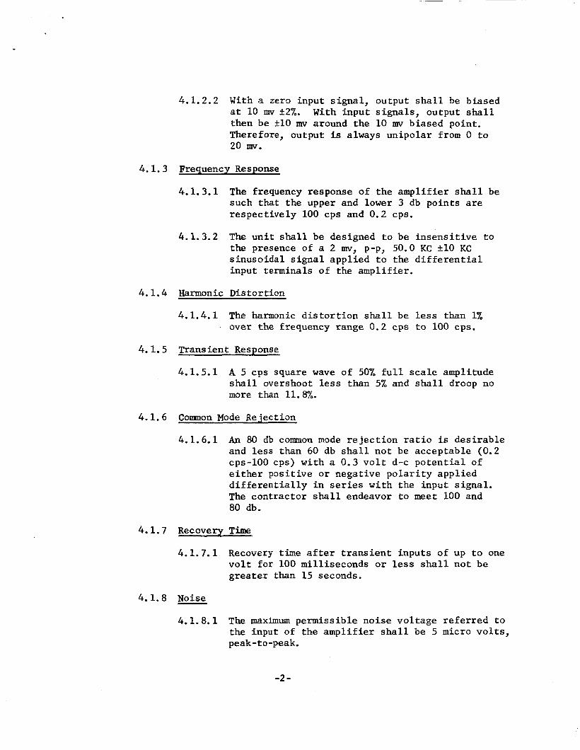
4.1.2.2 With a zero input s ignal , output s h a l l be biased a t 10 mv +2%. With input s ignals , output shall then be + lo mv around the 10 mv biased point. Therefore, output is always unipolar from 0 t o 20 mv.
4.1.3 Frequency Response
4.1.3.1 The frequency response of the amplif ier shall be such that the upper and lower 3 db points are respectively 100 cps and 0.2 cps.
4.1.3.2 The u n i t shall be designed t o be insens i t ive t o the presence of a 2 mv, p-p, 50.0 KC 210 KC sinusoidal s igna l applied t o the d i f f e r e n t i a l input terminals of the amplif ier .
4.1.4 Harmonic Distortion
4.1.4.1 The harmonic d i s t o r t i o n shall be less than 1% over the frequency range 0.2 cps t o 100 cps.
4.1.5 Transient Response
4.1.5.1 A 5 cps square wave of 50% f u l l scale amplitude shall overshoot less than 5% and s h a l l droop no more than 11.8%.
4.1.6 Cormnon Mode Rejection
4.1.6.1 An 80 db common mode r e j ec t ion r a t i o i s des i rab le and l e s s than 60 db s h a l l not be acceptable (0.2 cps-100 cps) with a 0.3 v o l t d-c po ten t i a l of either posi t ive o r negative po la r i ty applied d i f f e r e n t i a l l y i n series with the input s ignal . The contractor shall endeavor to meet 100 and 80 db.
4.1.7 Recovery T h e
4.1.7.1 Recovery tine after t r ans i en t inputs of up t o one v o l t for 100 milliseconds o r less shall not be grea te r than 15 seconds.
4.1.8 Noise
4.1.8.1 The maximum permissible noise vol tage re fer red t o the input of the ampl i f ie r shall be 5 micro vol t s , peak-to -peak.
-2 -

4.1.9 Gain - 4.1.9.1 The adjustable vol tage gain shall be 100-150.
4.1.10 Gain S t a b i l i t y
4.1.10.1 The gain shall no t vary more than 25% over any 12 hour period a t an ambient temperature of 75 degrees F 210 degrees a f t e r ten (10) minutes of warxnup.
4.1.11 Power
4.1.11.1 Prime power supplied t o u n i t from capsule power source w i l l be +10 vo l t s , d-c and -10 vo l t s , d-c 21%. R i p p l e and noise w i l l not exceed 0.01%.
4.1.11.2 R i p p l e content w i l l no t exceed .01%.
4.1.11.3 Current consumption shall be as small as p r a c t i c a l and no grea te r than 5 ma from each supply.
4.2 Physical Requirements
4.2.1 Weight
The weight of the conditioner shall not exceed 45 grams.
4.2.2 Dimens ions
Physical dimensions of the signal conditioner s h a l l not exceed 2.3 inches 39 1.5 inches by 0.390 inches.
4.2.3 Gain Control
The u n i t shall have a ga in con t ro l access ib le from the end when the connectors are attached. Clockwise r o t a t i o n shall r e s u l t in increasing gain.
4.3 Environment: The equipment shall be capable of performing satis- \ f a c t o r i l y during launch, o rb i t , reentry, and impact i n accordance 1
\ w i t h the t o t a l requirements of t h i s spec i f i ca t ion when subjected i
t o any n a t u r a l combination of the environments spec i f i ed herein.
4.3.1 S a l t Sea Atmosphere: The equipment s h a l l be capable of
i' .---
operation in a sal t sea atmosphere as spec i f i ed i n paragraph 5.3.1.7 herein.
4.3.2 S a l t Water Immersion: The equipment s h a l l be capable of operating continuously while subjected t o an immersion t e s t as spec i f i ed i n paragraph 5.3.1.12 herein.
-3-

4.3.3 Sand and Dust: The equipment shall be capable of operation i n a sand and dust atmosphere as spec i f ied i n paragraph 5.3.1.6 herein.
4.3.4 Fungus: The equipment shall be capable of operation a f t e r being subjected t o ambient conditions conducive t o fungus growth as spec i f ied i n paragraph 5.3.1.5 herein.
4.3.5 Pressure: The equipment shall be capable of operation while being subjected t o ambient pressure va r i a t ions from 1.0 t o 19.0 p s i a .
4.3.6 Temperature: The equipment shall be capable of operation while being subjected t o ambient temperature from Oo F. to +16OoF. The equipment shall withstand, without damage, nonoperational exposure t o ambient temperatures of +ZOOOF. and -6O0F.
4.3.7 Humidity: The equipment shall be capable of operation both during and a f t e r Subjection t o va r i a t ions i n r e l a t i v e humidity from 15 percent t o 100 percent.
4.3.8 Acceleration: The equipment shall be capable of operation both during and a f t e r subject ion t o the acce lera t ion specif ied i n paragraph 5.3.1.8 herein.
4.3.9 - Shock: The equipment shall be capable of operation a f t e r being subjected t o shock a s spec i f ied i n paragraph 5.3.1.9 herein.
4.3.i.O Vibration: The equipment shall be capable of operation while being subjected t o random vibra t ion as spec i f ied i n paragraph 5.3.1.10 herein.
4.3.11 E lec t r i ca l and Electronic Suscept ib i l i ty : shall be completely unaffected by conducted or rad ia ted signals as defined i n Ma-1-26600.
The equipment
4.3.12 Acoustic Noise: The equipment shall be capable of operation while being subjected t o acoust ic noise as spec i f ied i n paragraph 5.3.1.11 herein.
4.3.13 Oxygen Atmosphere: The equipment shall be capable of operation i n a 100 percent 0 atmosphere without any 2 de le te r ious e f fec ts t o the equipment and without emission of e i t h e r tox ic or obnoxious odors.
4.3.14 - Rain: The equipment shall be capable of withstanding a rainy atmosphere as described i n MIL-E-5272.
-4 -
4.3.15 Temperature - Altitude: The equipment shall be capable of operation while being subjected t o any combination of temperature -a l t i tude as spec i f i ed herein.
4.3.16 Voltage Variation: Operation of the equipment shall be unaffected when subjected t o vol tage va r i a t ions within the limits of paragraph 4.3 herein.
5. TESTREQUIREMENTS
5.1 C las s i f i ca t ion of Tests: The equipment shall be subjected t o the following tests which shall be conducted by the Contractor. Spec i f i c test plans, procedures, and test r e s u l t s shall be prepared and submitted by the Contractor t o NASA f o r approval.
5.1.1 Acceptance Tes ts : These tests are performed t o assure that the materials, workmanship, and performance of u n i t s t o be subjected t o design approval tests o r programned f o r de l ivery t o NASA are not f a u l t y and that the u n i t s have been manufactured t o approved drawings and speci- f i ca t ions . These tests are normally an inves t iga t ion of operating and nonoperating c h a r a c t e r i s t i c s under room ambient environmental conditions.
5.1.2 Design Approval Tests: These tests are conducted on preproduction equipment t o e s t a b l i s h that the u n i t s comply wi th a l l the requirements of t h i s Statement of Work. conditions i s inferred.
A complete test under operating environmental
5.2 Acceptance T e s t s
5.2.1 Examination: Each u n i t shall be examined t o determine conformance with t h i s exh ib i t wi th respec t t o materials, standard p a r t s , and workmanship.
5.2.2 Testing: Each uni t shall be t e s t ed t o determine compliance wi th the d e t a i l functional requirements of Section 4.0 of t h i s specification. These tests shall include, but are not l imi ted to, the following:
a. Size b. Weight c. Input characteristics d. Output c h a r a c t e r i s t i c s e. Power consumption f . Noise r e fe r r ed t o input.
-5 -

I 5.3 Design Approval Tests: These tests shall be performed on the
f i r s t production un i t s . on s a t i s f a c t o r y completion of these tests. t e s t i n g shall cons i s t of t he q u a l i f i c a t i o n tests out l ined herein. P r i o r t o conducting these tests, each u n i t shall be subjected to, and s h a l l meet the requirements of, the acceptance tests out l ined i n Section 5.2.
Release f o r production shall be based Design approval
5.3.1 g u a l i f i c a t i o n Tests: These tests shall be conducted by the Contractor and shall cons i s t of t he following tests. Two u n i t s shall be subjected t o these tests; however, both u n i t s w i l l not be required t o undergo a l l tests. Sequence and d i s t r ibu t ion of tests shall be determined by Contractor subject t o NASA approval.
5.3.1.1 Pressure: The equipment shall be placed in a chamber and the pressure reduced t o 1.0 p s i a . The equipment shall operate s a t i s f a c t o r i l y with the chamber temperature a t 160° F. f o r 1.5 hours. There s h a l l be no crushing, d i s to r t ion , opening of s ea l s , o r o ther damage de le t e r ious t o the proper operation, l i f e and s e r v i c e a b i l i t y of t h e equipment as a r e s u l t of t h i s test. R e p e a t a t 19.0 psia.
5.3.1.2 High Temperature: The equipment shall be subjected t o Procedure I1 of the high-temperature test of Specification MIL-E-5272, except t h a t operating time shall be continuous.
5.3.1.3 Low Temperature: The equipment s h a l l be placed i n the temperature chamber and the chamber cooled t o -60" F. After four hours i n t h i s environment, the equipment shall be inspected f o r evidence of deterioration. The chamber temperature shall then be raised t o and maintained a t O O F . After s t a b i l i - zation, the equipment shall be operated i n t h i s environment f o r a period of four hours.
5.3.1.4 Humidity: Per MIL-E-5272, Procedure I, except that operating time is continuous .
5.3.1.5 Fungus : P e r MIL-E-5272, Procedure I, (applicable only t o untreated and untested materials). This test need n o t be performed i f a document is sub- mitted s t a t ing that only nonnutrient materials are used.
-6 -

5.3.1.6 Sand and Dust: Per MIL-E-5272, Procedure I. This test need not be performed i f a dncument i s submitted s t a t i n g that the u n i t i s sealed and that the ex terna l f in i shes have been sub- jected t o Sand and Dust tests without detrimental r e su l t s .
5.3.1.7 S a l t Spray: Per MIL-STD-810 (USAF), Method 509. ~
5.3.1.8 Acceleration : Equipment shall be subjected t o the test determined t o be most s t r ingen t of those applicable t o the equipment. Equipment shall be tes ted i n each a x i s separately.
5.3.1.8.1 Launch: The equipment shall operate while receiving acce lera t ion along an ax i s parallel t o the longi tudinal spacecraf t a x i s (FWD) increasing l i n e a r l y from l g t o 7.25g i n 326 seconds.
5.3.1.8.2 Abort: The equipment shall be acceler- a ted once i n each d i r ec t ion along the three mutually perpendicular axes a t 7.25g f o r one second, while operating. (Loads do not combine).
5.3.1.8.3 Reentry: The equipment shall be accelerated with a 15.7g r e su l t an t acce lera t ion (15g longi tudinal and 4.5g l a t e r a l ) f o r 30 seconds i n each d i rec t ion along each of the two l a t e r a l axes a t the 16.7' r e s u l t a n t angle while operating.
5.3.1.9 Shock: A l l shock tests shall be a ha l f s ine wave pulse of 11 +1 millisecond duration.
5.3.1.9.1 Landing: Equipment shall operate satis- f a c t o r i l y following landing shock loads. The equipment shall be subjected t o s i x landing impact shocks, one i n each d i r ec - tion. These shocks cons i s t of those loads shown i n Figure 2.
i I
5.3.1.9.2 U l t i m a t e : Equipment shall be ult imate shock tes ted. Operation following the test i s not required; however, the equip- ment shall not break loose from i t s mount. The equipment shall be subjected t o s i x landing impact shocks, one i n each d i rec- tion. These shocks cons is t of those loads shown i n Figure 3.
-7-
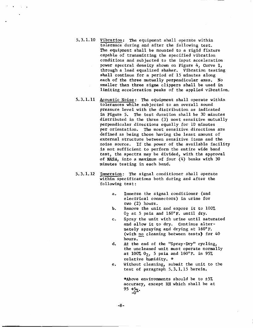
5.3.1.10
5.3.1.11
5.3.1.12
Vibration: The equipment shall operate within tolerance during and a f t e r the following test. The equipment shall be mounted t o a r i g i d f i x t u r e capable of t ransmi t t ing the spec i f i ed v ib ra t ion conditions and subjected t o the input acce lera t ion power spec t r a l dens i ty shown on Figure 4 , Curve I, through a load equalized shaker. shall continue f o r a period of 15 minutes along each of the three mutually perpendicular axes. No smaller than three sigma c l ippe r s shall be used i n l imi t ing acce le ra t ion peaks of the applied v ibra t ion .
Vibration t e s t i n g
Acoustic Noise : tolerances while subjected t o an ove ra l l sound pressure l e v e l with the d i s t r i b u t i o n as indicated i n Figure 5. The test duration shall be 30 minutes d i s t r ibu ted i n the three (3) most s e n s i t i v e mutually perpendicular d i r ec t ions equal ly f o r 10 minutes pe r o r ien ta t ion . The most s e n s i t i v e d i r ec t ions are defined as being those having the least amount of ex terna l s t r u c t u r e between s e n s i t i v e items and the noise source. I f the power of the ava i l ab le f a c i l i t y is not s u f f i c i e n t t o perform the e n t i r e wide band test, the spec t r a may be divided, wi th the approval of NASA, i n t o a maximum of four ( 4 ) banks with 30 minutes t e s t i n g i n each band.
The equipment shall operate within
Immersion: The s i g n a l conditioner s h a l l operate within spec i f ica t ions both during and a f t e r the following test:
a.
b.
C.
d.
e.
Immerse the s i g n a l conditioner (and e l e c t r i c a l connectors) i n ur ine f o r two (2) hours. Remove the u n i t and expose it t o 100% 02 a t 5 p s i a and 160'F. u n t i l dry. Spray the u n i t with u r ine u n t i l sa tura ted and allow it t o dry. na t e ly spraying and drying a t 160'F. (with - no cleaning between tests) f o r 40 hours. A t the end of the "Spray-Dry" cycling, the uncleaned u n i t must operate normally a t 100% 02, 5 p s i a and 160'F. i n 95% r e l a t i v e humidity. * Without cleaning, submit the u n i t t o the test of paragraph 5.3.1.15 herein.
Continue a l ter-
*Above environments should be t o i5% accuracy, except RH which shall be a t - _
95 +5%. -0
-8 -
5.3.1.13 Oxygen Atmosphere: The equipment shall be placed i n an atmosphere of 100 percent oxygen, a t ambient pressure and operated f o r 40 hours. For a t least two hours of t h i s period, the chamber temperature shall be +160° F. Performance outs ide of s p e c i - f i c a t i o n tolerance, v i s i b l e burning, c r e a t i o n of t ox ic gases, obnoxious odors, o r d e t e r i o r a t i o n of seals shall c o n s t i t u t e f a i l u r e t o pass the test.
5.3.1.14 E l e c t r i c a l and E lec t ron ic In t e r f e rences : The equipment shall be t e s t e d i n accordance wi th the s u s c e p t i b i l i t y tests of MIL-1-26600.
5.3.1.15 Endurance Test: One u n i t shall be subjec ted t o an endurance test which shall be conducted a t ambient pressure and a t least 120' F. f o r 336 hours. During t h i s time, t he u n i t shall be operating wi th simulated input s i g n a l s and normal output s ignals .
-9 -

' I .
APPENDIX 11
2.6.2 3 f a l e o r y
A biopotential electrode is often considered to be a simple electrical connect-
ion to the subject. This is not strictly true, since the electrode must convert
a flow of ions in tissue to an analogous flow of electrons within a metallic
conductor. In this respect, the biopotential electrode is a complicated trans-
ducer which must convert energy from one form to another without losing
information content. The ion flow is converted to a flow of electrons by
electrochemical reactions taking place at the electrode-tissue interface. Each
electrode may be considered a half-cell battery which generates an electrical
potential difference between the metallic electrode and the tissue. The mag- 2ec
nitude of the potential is determined by the nature of the metal of the electrode
and by the type and concentration of ions present at the tissue surface in the
area of contact. This half-cell potential is typically less than one volt, but
may reach a magnitude of three or more volts, and may be positive or negative.
2 . 6 . 3 Practical Biopotential Measurements
In practice, the measurement of small body currents would be very difficult
with two simple metal electrodes because of the instability of the half-cell
potential at either of the electrodes. The half-cell potential is dependent
upon a chemical equilibrium determined by the concentration of metal ions in
the solution in the immediate vicinity of the electrode. This concentration
is significantly higher at the electrode than anywhere else i n the electrolyte
solution, and any disturbance which would change the metal ion concentration
at the interface would change the half-cell potential in an analogous manner,
-1-

' 1 .
For example, i f the electrode were moved, tapped, or s l i g h t l y j igg led , the
so lu t ion would be disturbed a t the in te r face , moving some of the metal ions
i n t o thesolut ion and changing the ha l f -ce l l po ten t i a l accordingly. Such a
system i s very suscept ible t o motion a r t i f a c t s and would be unstable when
used t o make DC and l o w frequency measurements. While idea l ly no po ten t i a l
d i f fe rence should exis t between a pair of i den t i ca l e lec t rodes , it is not
uncommon t o measure 20-50 mi l l i vo l t s po ten t i a l d i f fe rence when s i l v e r
e lec t rodes a re applied t o t i s sues .
When an electrode h a l f - c e l l potent ia l i s modified by a changing concentra-
t i o n of ions a t the in t e r f ace , due e i the r to a flow of current through the
e lec t rodes o r due t o loca l chemical conditions, the e lec t rode i s said t o be
"polarized". An e lec t rode which i s severely polarized w i l l a c t ive ly impede 24
the current a t low frequencies and tends t o a c t as a f i l t e r . This r e s u l t s i n
an a l t e r ed frequency response and signal d i s to r t ion .
The chemical reac t ion responsible for t he e lec t rode h a l f - c e l l po ten t i a l may
be represented by the generalized chemical equation,
+ - M = M + e
Using the Nernst equation, the potent ia l developed by the electrode and the
ions i n the ge l is:
RT E = Eo + F log (M+)
-2 -

where
E =
EO=
R =
T =
F = + M =
observed potential
standard potential for half cell
gas constant
absolute temperature
coulombs per equivalent
ions present (molar concentration)
Tabie 2--3gives the standard electrode potentials of various elements;
customary to assign the zero potential to the hydrogen electrode.
it is
-3 -

Electrode
Lithium
Potassium
Sodium
Magnesium
Aluminum
Zinc
Iron
Cadmium
Nickel
Tin
Le ad
Hydrogen
Copper
Silver
P 1 at inum
Gold
43, AgCl, c1-
TABm 2-3
ELECTROMOTIVE SERIES FOR SOME ELECTRODES
Half Reaction
+ Li = Li + e- + K = K +e-
+ - Na = Na + e Mg = Mg* + 2e-
-Hi- AI = AI + 3e- Zn = zn* + 2e- Fe = Fe* + 2e- Cd = Cd* + 2e- NI = NI* + 2e- Sn = sn* + 2e-
ft Pb = Pb + 2e- + H2 = 2H + 2e- +f
Cu = Cu + 2e- = &* + 2e-
-Hi- AU = AU + 3e-
Electrode Potential (volts)
3.02
2.92
2.71
2.34
1.67
0.76
0.44
0.40
0.25
0.14
0.13
0.00
-0.34
-0.80
-1.20
-1.42
-0.22
-4 -

' .
Since s i l v e r i s o f t en used as a biological e lectrode ma te r i a l , it i s i n t e r e s t -
ing t o examine the consequences of placing a s i l v e r e lectrode i n contact with
t i s s u e . It may be assumed t h a t a pure s i l v e r e lec t rode , whose surface i s
covered with a t h i n coating of s i l ve r oxide, i s placed i n contact with an
e l e c t r o l y t i c soilution containing a known concentration of sodium and chlor ide
ions. I n t h i s model, a f t e r i n i t i a l contact , the small amount of s i l v e r oxide
a t the surface begins t o d isso lve t o produce a s m a l l concentration of s i l v e r
ch lor ide i n the solut ion. The existence of s i l v e r ions i n so lu t ion a t the
sur face of the me ta l l i c s i l v e r i s responsible f o r the generated h a l f - c e l l
po ten t i a l .
For t h e s i l v e r e lectrode the Nernst equation reduces to:
E = Eo + .0591 log (As+) ( a t 25OC)
I f another i den t i ca l e lectrode would be placed i n the so lu t ion , i t would
develop an iden t i ca l h a l f - c e l l po ten t ia l ,
measure the d i f fe rence between the two e lec t rodes , no d i f fe rence would be
observed, s ince the two ha l f c e l l s would be i d e n t i c a l and oppose each o ther i n
the c i r c u i t . I f an e l e c t r i c a l generator (e.g. , the hea r t ) were located i n the
so lu t ion , some d is tance away from t h e pos i t ion of t he e lec t rodes , the electrode
po ten t i a l d i f fe rence would be only due t o the generator, and thus the electrodes
would be capable of measuring the small ion cur ren ts produced by the generator.
I f an i d e a l voltmeter was used t o
The term "polarization", when applied t o b io logica l e lec t rodes i s usua l ly
used t o descr ibe changes i n e l e c t r i c a l po ten t i a l developed by the electrode-
t i s s u e in te r face . I n appl icat ions where s ign i f i can t cur ren ts flow through the
-5 -

electrodes (as in impedance pneumography) "polarization" refers to the various
changes caused by the current flow.
categories.
processes where metal or gaseous ions are removed from the solution. These
are encountered at low current densities.
occurs when the rate of ion production or utilization exceeds the rate of
diffusion of these ions in the solution, causing a concentration gradient.
Higher current densities are necessary to produce this type of potential shift.
The third category simply includes voltage changes at the electrodes due to
their resistance and the current flowing through them.
polarization processes occur at electrodes where significant current flows,
such as when electrodes are used for stimulating tissues, or during bio-
impedance measurements.
These changes may be classified in three
The first are changes caused by irreversible decomposition
The second polarization process
All three of these
A n electrode can develop artifact signals often indistinguishable from polar-
ization effects under circumstances not necessarily caused by the flow of
electrical current.
by chemical changes at or near the metal-electrolyte interface, which alter
the concentration of the metallic ion. This is sometimes called F'chemical
polarization". In general, the difficulties encountered in the use of
electrodes in measuring biopotentials are more likely the result of these
local electrochemical effects than of true current polarization.
The potential developed by the electrode may b e affected
-6-

I .
DIF'FERENTIAL FIELD EFFECT TRANSISTOR AMPLIFIER ANALYSIS
I. Comaon-Mode Rejection
The canrmon-nmde r e j e c t i o n r a t i o is of t en erroneously considered t o be
simply the r a t i o of d i f f e r e n t i a l t o camnon-mode gain.
the common-mode r e j e c t i o n ratio is l imi t ed due t o c t r c u i t unbalances.
I n t h i 8 ana lys i s , we derive the usual expressions f o r small signal
d i f f e r e n t i a l ampl i f ie r gain and, by the method of Middlebrook,
der ive an expression f o r the l a rges t common-de r e j e c t i o n r a t i o poss ib le
I n prac t ice ,
i n the presence of simultaneous
c i r c u i t ?+a
c i r c u i t unbalances i n rp and &,,.
A 4 Model
Figure One - F.E.T. Amplifier and Model
h iddlebrook, R. D. M f f e r e n t i a l Amplifiers, W i l g & Sone, New York, 1963.
-1-

For differential input signals, the voltage across R does not change and
i t may be replaced by a short circuit. The following model then applies:
Figure TrJot Model for Differential Input Signals
Once having observed relations ( l ) , (Z), and (3, the analysis i s Simple-
Thus, the differential gain is given by,
-2-

The following model holds for common-mde signals.
s, I
Figure Three, Model for Common-Mode Input Signale
Because R is now included, another meah is introduced into the model and an
additional equation i s required. Note that the value of R ie doubled as two
identical comnon-mode currents flow through it. The analysis proceeds as
follows :
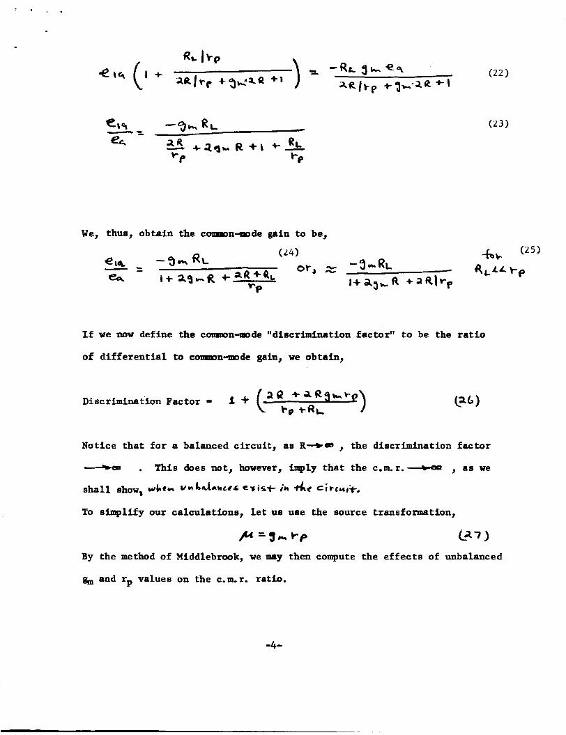
W e , thus, obtain the cormron-mode gain to be,
I f we now define the cormron-=de "discrimination factor" t o be the r a t io
of different ia l to common..mDde gain, we obtain,
a g + a R 3 b r ~ + k Discrimination Factor =
Notice that for a balanced circuit, as R*@ , the discrimination factor
-Q . This does not, however, imply that the c.m.r.- , as we
shal l show, when V ~ ~ & ~ C ~ ~ C~is-4- h Ai circ*,+,
To simplify our calculations, l e t us use the source transformation,
F = 3 h PP CAT J By the method of Middlebrook, we may then compute the effects of unbalanced
&,, and rp values on the c.m.r. ratio.
-4-

After the source transformation we find the following model to be true,
4 4, i*
et = &-pip,, L2 E.) e a = &fi ViJ. eo 0
LW)
We introduce tm, additional generators into the model, e1 and e2, to
account for the unbalanced g,,, and rpo
If we le t ,
and,
we find that,
t -
We make an approximation by using the tloriginalll values for $ and Vg( a8, zq),
th i s i e equivalent to ignoring higher order terms.
The derivation of the gain equations proceeds as derived ear l ier , except
that we include e l a d e2.
v=v3 +ieaR V] = -+SL c3 6 1 -5-

Now ipco is the comnimode plate current value with
similarly,
e l = 0 and e2 = 0.
(34 1
Now, solving for the differential output voltage Vld we observe the effects
of unbalance.
Input voltage!
A differentbl output voltage results from a cormron-mde
t43)
-6-

where two types of "cross terms" are evident.
ratio %a then,
The colmnon-mode rejection
If we l e t R QD , we find that,
-7-

" . .
'If we then return to the controlled voltage source =del we again use,
" 3 d p '1
Thus,
Thus for R-,
-8-
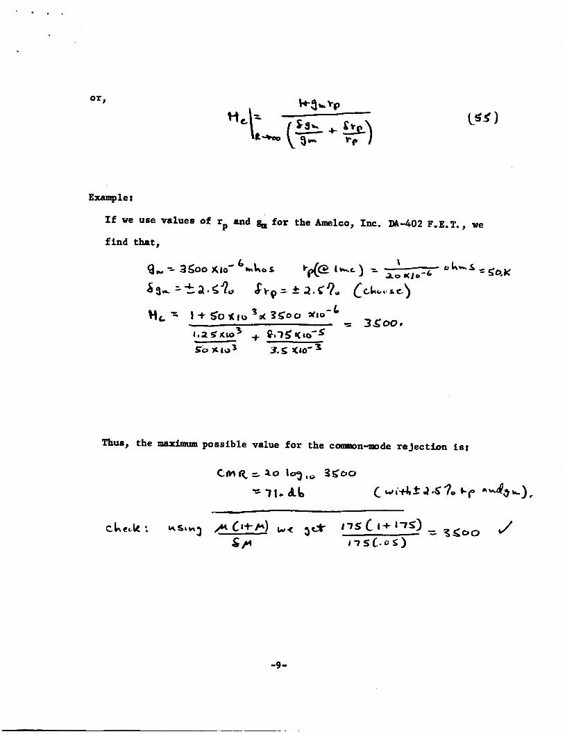
Example:
Thus7 the maximum poss ib le value for the conrmon-amde rejection is:
-9-

Of?
Example:
Thus, the maximum possible value for the cormPon..IPode rejection i e :
-9 -

APPENDIX IV
11. Recovery Time Analysis
We define the recovery time, for the amplifier shown in Figure 10, to
be the time in which the differential amplifier output signal returns
to 210. millivolts of the normal 10. mv output offset. The recovery
time shall be measured by introducing a differential input signal of
one volt for 100. milliseconds. Our design goal for the EEG amplifier
shall be a recovery time of 6.0 seconds.
Since the gain of the first stage is on the order of 3.0, we use small
signal analysis. The second stage, however, has a gain of fifty, and
in response to a one volt input pulse, will be cut off or saturated.
In the second stage we must, therefore, use large signal techniques.
Figure 5 shows our model for the EEG amplifier.
are differential.
All voltages noted
Figure Five: Amplifier Circuit Model
-1 -

Figure 6 shows circuit waveforms for the first and second stages. Since
the first stage operates in a small signal mode, the output is simply
the gain times the input. C1 and R1 are the effective circuit values.
The value for R1 includes the input resistance of stage two and the out-
put resistance of stage one.
the relationship of 3; = RlCl to the input pulse width.
Ex from,
The waveform,ec, is primarily determined by
We may compute
where,
t = .1 sec. and A = 3.0 volts
Now,- must be,
and for f = . 2 cps,
7 = .8 sec.
Thus,
E: = 3.0 e - 0 1 / 0 8 = 2.65 volts X
and,
s e = 3.0 - 2.65 = .35 volts
Due to the high gain of stage two, large signal analysis is required. The
two sides of the stage are driven, respectively, into cutoff and satura-
tion for any input signal greater than or equal to k.2 volts. The output
dynamic range of stage two is k10.0 volts. For the positive going portion
of ec, ed will remain cuttoff at +IO. volts. For the negative going por-
tion of e,, ed will remain at -10.0 volts until e, is less than -.2 volts.
This occurs at time tl. To find tl,
-2 -


e,= S e * e -t/*8 t > .1 When t = tl, e, = .2 volts.
.2 = .35e -ti/ .8 Thus,
or, tl = .8 (Ln 1.75)
ti = .45 sec.
Referring to Figure 7, the level, Ey, may be computed as we previously
computed E,.
Ey = 10 e = 8.8 volts
Thus,
b e e = 1.20 volts.
The level, E, , may be computed:
E, = 11.2 e -.45/.8
assuming that R1Cl = R2C2 = .8 sec.
so,
E= = 6 . 4 volts.
By the linear property of the passive bilateral coupling circuit R C
we can now disassemble ed into its component waveforms, Figure 8, and
compute e, as the sum of the component responses.
2 2'
The component responses are all obvious except the response to component IV.
-4 -


-6-
' . , , I
I I
I C
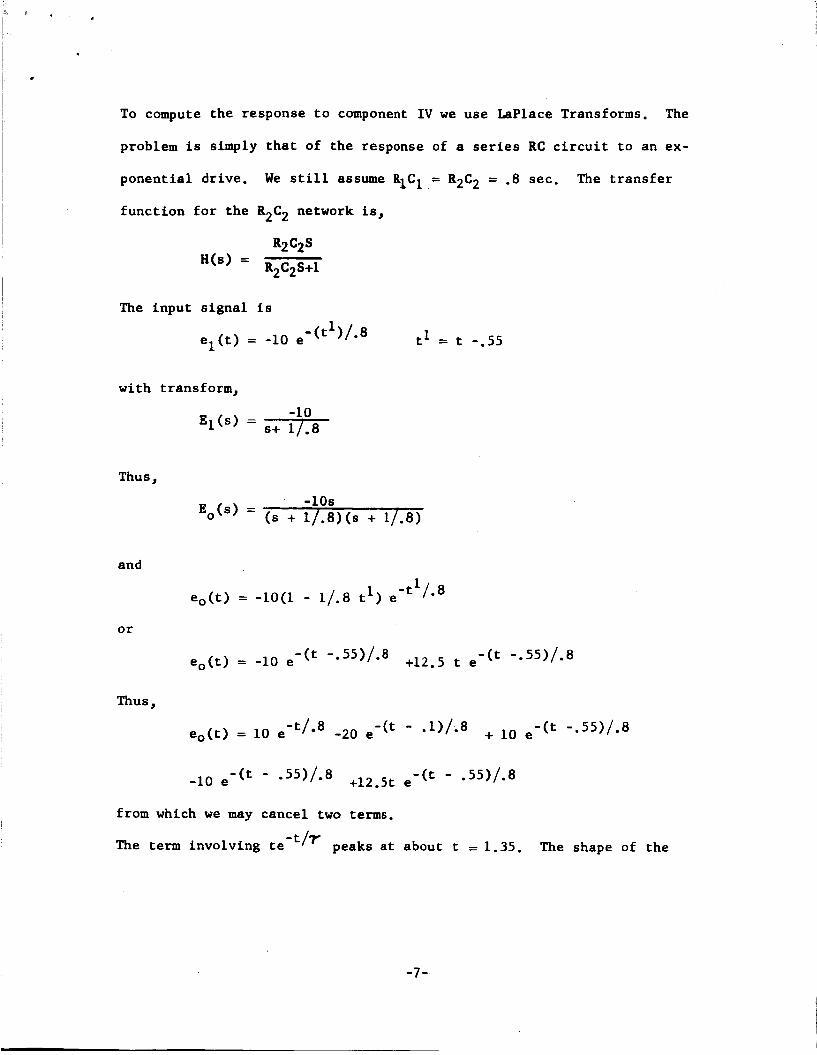
To compute the response to component IV we use Laplace Transforms. The
problem is simply that of the response of a series RC circuit to an ex-
ponential drive.
function for the R2C2 network is,
We still assume RICl = R2C2 = .8 sec. The transfer
R2C2S H(s ) = R2C2S+1
The input signal is
tl = t -.55
with transform,
q ( s ) = -&- Thus,
-10s = (s + 1/.8)(s + 1/.8)
and 1
eo(t) = -10(1 - 1/.8 tl) e-t /08
or
Thus,
from which we may cancel two terms.
The term involving te -t/r peaks at about t = 1.35. The shape of the
-7 -

transient response beyond t = 1.0
A plot of the final output waveform follows in Figure 9.
stage is a d.c. coupled emitter follower, ef = ee.
is strongly influenced by this term.
Since the last
I
-8-

.
?? B P
-. + $ < O , + & & & t f = ; N O - m
I- I ? . N
1 1 1 I I I (D 3 I a
Y
t
L.
0
N
m Y
-9 -


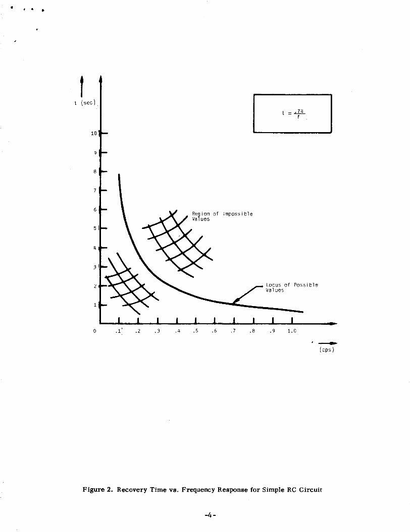
APPENDIX v.
Appendix V.& Recovery Time - Frequency Response Relationship
A. A Simple Case
To determine the in t e r r e l a t ionsh ip between frequency response and
recovery time, w e w i l l f i r s t consider the s imple , highpass f i l t e r ,
o r coupling network shown i n Figure 1.
Figure 1. S imple Coupling Network
The f i l t e r 3 db down frequency, fl, i s given by,
(1) w R C = 1
w h e r e ur= 2 r r f l (2)
o r L fl = 2 V R C
(3)
W e define the recovery t i m e , ti, f o r such a network, t o be the
time required f o r the output t o se t t le t o within an a r b i t r a r y
voltage d i f fe rence (e.g. k 10. mv) from i t s quiescent output
l e v e l (zero), a f t e r an input pulse (e.g., 1 v o l t f o r 100 m.s . ) .
The simple t r a n s i e n t shown i n Figure 1 is given by, - e2 = Ae ", Y = RC
The recovery time, ti, is then, f o r e2 = 10. mv,
(4)
-1 -

For t h i s s imple c i r c u i t , with A = 1, the recovery t i m e and low
frequency 3 db point are related by,
4.61
Although t h i s c i r c u i t is exceedingly simple, it serves t o i l l u s -
trate the s t rong re la t ionship between recovery time and frequency
response. The equation (7) is p lo t ted i n Figure 2. The r e l a t ion -
sh ip shown i n Figure 2 is obviously hyperbolic. It is in t e re s t ing
t o note that only the points on the locus are possible sets of
values.
B. The EEZ Amplifier
In the s imple example above, the desired spec i f i ca t ions a r e m e t .
There are four important differences between the f u l l EEG a m p l i -
f i e r design and the simple RC c i r c u i t that makes t h i s impossible,
however :
1. The amplif ier has a gain, 100-150,
2. The ampl i f ie r has dynamic range l i m i t s a t the supply voltages,
+lo. vo l t s , and
3. The ampl i f ie r must have two RC coupling networks.
Differences 1 and 2 are self-evident. L e t us, a t t h i s point,
j u s t i f y (3). Since the amplifier must operate with a d i f f e r e n t i a l
d.c. input s i g n a l of one vol t , it is obvious t h a t the f i r s t s tage
can have a gain no greater than 3. a d must be a.c. coupled t o the
second stage. I f this coupling network were omitted, the required
gain of 100-150 would cause the ampl i f ie r to be driven in to cutoff
-2 -

I
o r s a t u r a t i o n a t the gain stage.
is a l s o necessary t o m e e t t he d i f f i c u l t k200. pv. ou tput -of fse t -
temperature spec i f ica t ion . This requirement is equivalent t o
about 5 pv./OC and can be m e t by a s i n g l e e m i t t e r follower, output
stage.
avoid the temperature d r i f t of the gain stage.
could not be improved by the use of a high gain s tage with feed-
back as t h e tempera ture d r i f t would s t i l l be an equivalent input
d r i f t mul t ip l ied by the amplifier gain.
A second RC coupling network
The output stage must be RC coupled t o the ga in s t age t o
This s i t u a t i o n
I n Appendix I1 of Progress Report I, w e found an expression f o r
the ampl i f ie r output t rans ien t ,
I f we take the logarithm of both s ides of equation 8 t o so lve f o r
-2 ( a t t = tl, e = 10 1, -
tl C21ntl = -Cl, (9)
we discover that t h e equation i s transcendental. It would no t be
c o r r e c t t o expand the logarithm i n a series unless a l a rge number
of terms were used. W e , thus, cannot ob ta in a closed form a n a l y t i -
cal so lu t ion t o the re l a t ionsh ip between recovery time and frequency
response f o r t he f u l l c i r cu i t . W e can of course obta in experimental
r e s u l t s , and these are shown i n Figure 3.
-3 -
t t (sec )
10
9
0
7
6
5
U
3
2
1
0
I
Locus o f Poss Values
i ble
.l' .2 . 3 .4 .5 .6 .7 .E .9 1.0
Figure 2. Recovery Time vs. Frequency Response for Simple RC Circuit
-4 -

t
t Sec'
t 13
12
11
10
9
0
7
6
5
4
3
2
1
I I 4 ) c -
I I Measurement Error
Estimate
I I 1 I 1 I 1 I 1 1 1 1 1
cps ' f -
Figure 3. EEG Recovery Time vs. Frequency Response
-5- ~