Field-Effect Transistors Based on Zinc Oxide Nanoparticles · Field-Effect Transistors Based on...
73
José Tiago Macedo de Carvalho Licenciado em Engenharia de Micro e Nanotecnologias Field-Effect Transistors Based on Zinc Oxide Nanoparticles Dissertação para obtenção do Grau de Mestre em Engenharia de Micro e Nanotecnologias Orientador: Doutor Luís Miguel Nunes Pereira, Professor Auxiliar, Faculdade de Ciências e Tecnologia da Universidade Nova de Lisboa Júri: Presidente: Professor Doutor Rodrigo Ferrão de Paiva Martins Arguente: Prof. Doutor Pedro Miguel Cândido Barquinha Vogal: Prof. Doutor Luís Miguel Nunes Pereira Setembro 2015
Transcript of Field-Effect Transistors Based on Zinc Oxide Nanoparticles · Field-Effect Transistors Based on...

José Tiago Macedo de Carvalho
Licenciado em Engenharia de Micro e Nanotecnologias
Field-Effect Transistors Based on Zinc Oxide Nanoparticles
Dissertação para obtenção do Grau de Mestre em Engenharia de Micro e Nanotecnologias
Orientador: Doutor Luís Miguel Nunes Pereira, Professor Auxiliar, Faculdade de Ciências e Tecnologia da Universidade Nova de Lisboa
Júri:
Presidente: Professor Doutor Rodrigo Ferrão de Paiva Martins Arguente: Prof. Doutor Pedro Miguel Cândido Barquinha Vogal: Prof. Doutor Luís Miguel Nunes Pereira
Setembro 2015


Field-Effect Transistors Based on Zinc Oxide Nanoparticles
© José Tiago Macedo de Carvalho
Faculdade de Ciências e Tecnologia
Universidade Nova de Lisboa
A Faculdade de Ciências e Tecnologia e a Universidade Nova de Lisboa têm o direito, perpétuo e sem limites geográficos, de arquivar e publicar esta dissertação através de exemplares impressos reproduzidos em papel ou de forma digital, ou por qualquer outro meio conhecido ou que venha a ser inventado, e de a divulgar através de repositórios científicos e de admitir a sua cópia e distribuição com objetivos educacionais ou de investigação, não comerciais, desde que seja dado crédito ao autor e editor.


Field-Effect Transistors Based on Zinc Oxide Nanoparticles i
ACKNOWLEDGMENTS
This master thesis represents for me one of the most exciting experiences that I have been
during this academic journey in the degree of Micro and Nanotechnology Engineering at FCT-UNL.
Many memories, friendships, uncertainties, good and bad times are also part of this whole journey.
Hopefully, I have not being travelling alone and accordingly I would like to thank all the people who
supported, encouraged and made my journey a memorable one.
First, it was a privilege to be able to integrate in a creative and prestigious team like
CENIMAT|i3N and CEMOP. A restless demand in order to overcome barriers and open new horizons
in scientific knowledge are a constant in these centers, developing innovative, challenging and current
work applied in different areas. Therefore, first of all I would like to thank Professor Rodrigo Martins and
Professor Elvira Fortunato for the access to these installations and technology. Their multidisciplinary
knowledge, competence and commitment allow the excellent conditions of work here in CENIMAT|i3N
and CEMOP. In addition, I would like to thank for the fact of being able to open this unique and
outstanding integrated masters in Portugal.
Secondly, I would like to express my sincere gratitude to my supervisor, Professor Luís Pereira
for accepting and give me the chance to join and work in his research group. I cannot thank you enough
for all support, encouragement, valuable suggestions, availability and the spirit of research, your
inspiring enthusiasm and the Wednesday brainstormings. I am also grateful for all the support given by
his extraordinary group of researchers including Paul Grey, Inês Cunha, Diana Gaspar, Lidia Santos,
as well as Raquel Barras, Ivan Garcia, João Simões and Pedro Freitas his master students. Thank you
guys for all the advices, knowledge, the inspiring long hours of hard-working spent in the Lab 5, 6, 7,
the never ending optimism, the laughs, the patience with me and of course for keeping the NPT
conditions. To Paul and Lidia for inorganic EGTs and printing support and Inês and Diana for cellulose
and cleaning room support too. Thank you for always finding time to discuss the things that you guys
well know. Once again, thank you Paul for your relevant and innovative suggestions and for always find
time to help in every possible way. Essentially, thanks to all of you and especially to Professor Luís for
installing this team and work spirit. Words are not enough to express all my gratitude to all of you, I am
truly glad to meet you and I will remember you for the rest of my life.
In addition, I would like to thank Beatriz, Miguel and Sofia who had the opportunity to attend the
course MCP and thus had the chance to follow and contribute with relevant suggestions for the
development of this work.
I would like also to express my gratitude to Alexandra Gonçalves, Ana Crespo, Ana Pimentel,
Ana Santa, Antónia Conceição, Carolina Marques, Cristina Fernandes, Daniela Nunes, Daniela
Salgueiro, Joana Vaz Pinto, Marta Ferreira, Professor Rui Igreja, Raquel Martins, Ricardo Ferreira, Rita
Branquinho, Sónia Pereira, Tiago Mateus and Tomás Calmeiro, which always provide support in the
tasks related to technical support, data analysis, as well as, valuable suggestions relevant for this work.
In order to not forget anyone I would like to express my gratitude to the rest of these both
institutes for the support and the relevant suggestions.
Also, I am a grateful to my colleagues and course mates of Micro and Nanotechnology and
Materials Science as well. Thanks for the support with the tasks from those different areas during this
degree.
To my closest friends, Diogo, Emanuel, Inês, Raquel, Paul, Farah, Pedro, Davide, Vera, Silvia,
André, Cátia, Isabel, and all of the others who made these six years a memorable ones. What a great
time we had together!
I dedicate this work to my parents Rodrigo and Emilia and my sister Cristina as well, who always
support and encourage me. They are everything to me.

Field-Effect Transistors Based on Zinc Oxide Nanoparticles ii

Field-Effect Transistors Based on Zinc Oxide Nanoparticles iii
ABSTRACT
This work reports the development of field-effect transistors (FETs), whose channel is based on
zinc oxide (ZnO) nanoparticles (NPs). Using screen-printing as the primary deposition technique,
different inks were developed, where the semiconducting ink is based on a ZnO NPs dispersion in ethyl
cellulose (EC). These inks were used to print electrolyte-gated transistors (EGTs) in a staggered-top
gate structure on glass substrates, using a lithium-based polymeric electrolyte.
In another approach, FETs with a staggered-bottom gate structure on paper were developed
using a sol-gel method to functionalize the paper’s surface with ZnO NPs, using zinc acetate dihydrate
(ZnC4H6O4·2H2O) and sodium hydroxide (NaOH) as precursors. In this case, the paper itself was used
as dielectric.
The various layers of the two devices were characterized using X-ray diffraction (XRD),
scanning electron microscopy (SEM), Fourier Transform Infrared spectroscopy (FTIR),
thermogravimetric and differential scanning calorimetric analyses (TG-DSC). Electrochemical
impedance spectroscopy (EIS) was used in order to evaluate the electric double-layer (EDL) formation,
in the case of the EGTs.
The ZnO NPs EGTs present electrical modulation for annealing temperatures equal or superior
to 300 ºC and in terms of electrical properties they showed On/Off ratios in the order of 103, saturation
mobilities (µSat) of 1.49x10⁻¹ cm2(Vs)-1 and transconductance (gm) of 10-5 S.
On the other hand, the ZnO NPs FETs on paper exhibited On/Off ratios in the order of 102, µSat
of 4.83x10- 3 cm2(Vs)-1and gm around 10-8 S.
Keywords: Zinc oxide, ethyl cellulose, electrolyte-gated transistor, printed electronics, screen-printing,
sol-gel, paper electronics.

Field-Effect Transistors Based on Zinc Oxide Nanoparticles iv

Field-Effect Transistors Based on Zinc Oxide Nanoparticles v
RESUMO
Este trabalho reporta o desenvolvimento de transístores de efeito de campo (FETs), cujo canal
é constituído por nanoparticulas (NPs) de óxido de zinco (ZnO). Assim, mediante o uso da técnica de
impressão screen-printing, foram usadas e desenvolvidas tintas, uma das quais a semicondutora que
consiste numa dispersão de NPs de ZnO em etilcelulose (EC). Assim imprimiram-se, num substrato de
vidro, electrolyte-gated transistors (EGTs) numa estrutura staggered-top gate usando um eletrólito
polimérico à base de lítio.
Numa outra abordagem, num substrato de papel foram desenvolvidos FETs numa estrutura
staggered-bottom gate, recorrendo-se ao método sol-gel para funcionalizar a sua superfície, com NPs
de ZnO, através de dois percursores acetato de zinco dihidratado (ZnC4H6O4·2H2O) e hidróxido de
sódio (NaOH). Para estes dispositivos o papel foi usado como dielétrico.
As diferentes camadas que compõem os dois tipos de dispositivos foram caracterizadas por
difração de raio-x (XRD), microscopia eletrónica de varrimento (SEM), espectroscopia no infravermelho
por transformada de Fourier (FTIR), análise termogravimétrica e calorimetria diferencial de varrimento
(TG-DSC). A espectroscopia de impedância eletroquímica (EIS) foi usada para avaliar a formação das
electric double-layers (EDLs) no caso dos EGTs.
Os ZnO NPs EGTs apresentaram modulação elétrica para temperaturas de recozimento iguais
e superiores a 300 °C e em termos de propriedades elétricas apresentaram razões On/Off na casa dos
103, mobilidade de saturação (µSat) de 1.49x10⁻¹ cm2(Vs)-1 e transcondutância (gm) de 10-5 S.
Por outro lado, os FETs desenvolvidos no papel apresentaram uma razão On/Off que ronda os
102, uma µSat de 4.83x10- 3 cm2(Vs)-1e gm 10-8 S.
Palavras-chave: Óxido de zinco, etilcelulose, electrolyte-gated transistor, eletrónica impressa, screen-
printing, sol-gel, eletrónica em papel.

Field-Effect Transistors Based on Zinc Oxide Nanoparticles vi

Field-Effect Transistors Based on Zinc Oxide Nanoparticles vii
LIST OF ABBREVIATIONS
a.u. – Arbitrary units
AC – Alternating current
AFM – Atomic force microscopy
ATR-FTIR – Attenuated total reflectance - Fourier transform infrared spectroscopy
CE – Counter electrode
CEMOP – Centro de Excelência de Optoelectrónica e Microeletrónica de Processos
CENIMAT|i3N – Centro de Investigação de Materiais|Instituto de Nanoestruturas, Nanomodelação e
Nanofabricação
CPE – Constant phase element
CSPE – Composite solid polymer electrolyte
CV – Cyclic voltammetry
DI – Deionized
DSC – Differential scanning calorimetry
EC – Ethyl cellulose
ECM – Equivalent circuit model
ECT – Electrochemical transistor
EDL – Electric double-layer
EDLT – Electric double-layer transistor
EGT – Electrolyte-gated transistor
EIS – Electrochemical impedance spectroscopy
EtOH – Ethanol
FET – Field-effect transistor
FNG – Flexible nanogenerator
FSR – Felix Schoeller raw
FWHM – Full width at half-maximum
GZO – Gallium zinc oxide
ICDD – International centre for diffraction data
IPA – Isopropanol
ITO – Indium Tin Oxide
MIF – Metal ion free
MOSFET – Metal-oxide-semiconductor field-effect transistor
MW – Molecular weight
NPs – Nanoparticles
NRs – Nanorods
OFETs – Organic field-effect transistors
OLEDs – Organic light emitting devices
PE – Printed electronics
PET – Polyethylene terephthalate
PVD – Physical vapour deposition
RE – Reference electrode
RT – Room temperature
S/D – Source and drain
SEM – Scanning electron microscope
STA – Simultaneous thermal analyzer
TFT – Thin film transistor
TG – Thermogravimetry
UV – Ultra-violet
WE – Working electrode
XRD – X-ray diffraction

Field-Effect Transistors Based on Zinc Oxide Nanoparticles viii

Field-Effect Transistors Based on Zinc Oxide Nanoparticles ix
LIST OF SYMBOLS
𝜏𝑓 – Fall time
𝜏𝑟 – Rise time
µFE – Field-effect mobility
µSat – Saturation mobility
Cb – Electrolyte bulk capacitance
CDL – Capacitance of electric double-layer
Ceff – Effective capacitance
Ci – Capacitance of the dielectric layer
gm – Transconductance
IDS – Drain current
IGS – Gate leakage current
Im (Z) – Imaginary part of impedance
IOff – Off state current
IOn – On state current
L – Channel length
Rb – Electrolyte bulk resistance
Re(Z) – Real part of impedance
Rext – Exterior contact resistance
rms – Root mean square
Ss – Subthreshold swing
VDS – Voltage between drain and source
VGS – Voltage between gate and source
VOn – Turn-on voltage
VTh – Threshold voltage
W – Channel width
Y0 – Capacitance of a constant phase element
Z – Impedance
α – Fractal surface character
ρ – Bulk resistivity
σ – Electrical conductivity
σi – Ionic conductivity

Field-Effect Transistors Based on Zinc Oxide Nanoparticles x

Field-Effect Transistors Based on Zinc Oxide Nanoparticles xi
TABLE OF CONTENTS
ACKNOWLEDGMENTS ..................................................................................................................... I
ABSTRACT .......................................................................................................................................III
RESUMO ........................................................................................................................................... V
LIST OF ABBREVIATIONS ............................................................................................................. VII
LIST OF SYMBOLS.......................................................................................................................... IX
TABLE OF CONTENTS.................................................................................................................... XI
LIST OF FIGURES ......................................................................................................................... XIII
LIST OF TABLES ............................................................................................................................ XV
MOTIVATION ................................................................................................................................ XVII
OBJECTIVES ............................................................................................................................... XVIII
1. INTRODUCTION .........................................................................................................................1
1.1. Zinc oxide: Main features, structures and its application in electronics .............................1
1.2. Transistor technologies and electrolyte-gated transistors ..................................................2
1.3. Printed electronics and printing techniques .........................................................................3 1.3.1. Ink formulation and properties for thick films ......................................................................5
1.4. Inorganic field-effect transistors on paper ............................................................................5
2. MATERIALS AND METHODS: FABRICATION, OPTIMIZATION AND CHARACTERIZATION PROCESS OF EGTS AND FETS .......................................................................................................7
2.1. ZnO NPs ink formulation materials and reagents .................................................................7
2.2. ZnO semiconductor layer by sol-gel method ........................................................................7
2.3. Fabrication and optimization of the ZnO NPs EGTs and paper ZnO NPs FETs ...................7 2.3.1. ZnO NPs EGTs by screen-printing .....................................................................................7 2.3.2. Paper ZnO NPs FETs ........................................................................................................8
2.4. Characterization techniques ..................................................................................................8
3. RESULTS AND DISCUSSION ................................................................................................... 11
3.1. Characterization and properties of ZnO NPs ink semiconducting layer ............................ 11 3.1.1. Rheological measurements.............................................................................................. 11 3.1.2. TG-DSC of the vehicle and ZnO NPs ink ......................................................................... 12 3.1.3. ATR-FTIR of the ZnO NPs ink.......................................................................................... 13 3.1.4. Structural and morphological analysis of ZnO NPs ink ..................................................... 14
3.2. Characterization and properties of paper ZnO NPs semiconducting layer ....................... 15 3.2.1. Structural and morphological analysis of paper coated by ZnO NPs ............................. 15
3.2.2. FTIR of the paper coated by ZnO NPs ............................................................................. 16
3.3. Characterization and properties of lithium based polymer electrolyte .............................. 16 3.3.1. Electrochemical Impedance Spectroscopy of the electrolyte............................................. 17 3.3.2. Cyclic voltammetry of the electrolyte ................................................................................ 18
3.4. Characterization by EIS of the Felix Schoeller raw paper as dielectric layer for FETs ..... 19

Field-Effect Transistors Based on Zinc Oxide Nanoparticles xii
3.5. Considerations about the selected electrical contacts for ZnO NPs EGTs ....................... 20
3.6. Electrical contacts for paper ZnO NPs FETs ....................................................................... 21
3.7. Electrical charcaterization of ZnO NPs EGTs ...................................................................... 22 3.7.1. The working principle of the built ZnO NPs EGTs ............................................................. 22 3.7.2. ZnO NPs EGTs................................................................................................................ 23
3.8. ZnO NPs ink as UV photodetector ....................................................................................... 29
3.9. Electrical characterization of paper ZnO NPs FETs ............................................................ 30
4. CONCLUSIONS AND FUTURE PERSPECTIVES ..................................................................... 33
4.1. Final conclusions ................................................................................................................. 33
4.2. Future perspectives.............................................................................................................. 34
5. BIBLIOGRAPHY ....................................................................................................................... 37
6. ANNEX ...................................................................................................................................... 43

Field-Effect Transistors Based on Zinc Oxide Nanoparticles xiii
LIST OF FIGURES
Figure 1.1 – Three applications of ZnO nanostructures a) as an UV photodetector[24], b) as an anti-bacterial agent[25] and c) as a flexible nanogenerator (FNG).[26] ................................................1
Figure 1.2 – a) Cross-section schematic representation of the staggered top-gate structure with interdigital source and drain contacts adopted for the fully printed ZnO NPs EGTs on glass substrate. The respective EDL formations at each interface is also illustrated. b) A 3D schematic representation, where bottom black and top silver layers are the source/drain and gate electrodes, respectively. Whereas the white and the yellow layers represent the ZnO NPs and the composite solid polymer electrolyte (CSPE) film, respectively. ......................................................................3
Figure 1.3 – Schematic representation of the custom-made screen-printing present in CENIMAT|i3N laboratorys. Adapted from[65]. .....................................................................................................4
Figure 1.4 – a) An image of the developed FETs in CENIMAT|i3N where paper was applied as substrate and dielectric and b) its schematic representation. Adapted from[13]. ...........................................6
Figure 2.1 – Schematic representation of the ITO interdigital S/D electrodes patterned via photolithography. .........................................................................................................................8
Figure 2.2 – Schematic representation of the developed fully-printed ZnO NPs EGTs. ........................8 Figure 2.3 - Schematic representation of the developed paper ZnO NPs FETs. ..................................8 Figure 3.1 – Viscosity as function of the sear rate for ZnO NPs Ink, vehicle (EC 5 wt% on
toluene/ethanol) and lithium- based polymer electrolyte. ............................................................. 11 Figure 3.2 –TG-DSC curves of a) vehicle solution (EC 5 wt% on Toluene/ EtOH and b) ZnO NPs Ink.
.................................................................................................................................................. 12 Figure 3.3 - ATR-FTIR spectra of the ZnO NPs ink after being screen-printed and annealeted at 24, 300
and 450 °C. ................................................................................................................................ 13 Figure 3.4 – a) The topographical view, obtained by SEM, of the top surface and XRD diffractogram, at
30, 300, 350 and 500 °C, of ZnO NPs Ink, b) SEM picture of the ZnO NPs dispersed in ink, and c) the corresponding 3D view of the top surface, with an area of 25 µm2 acquired by AFM. ............ 14
Figure 3.5 – a) The topographical view, obtained by SEM, of the top surface and XRD diffractogram, of FSR paper after being functionalized through the sol-gel method, b) and c) amplified view of the cellulose fibers and the different obtained nanostructrues of ZnO, respectivelly. ......................... 15
Figure 3.6 – a) ATR-FTIR spectra of the Felix Schoeller raw (FSR) paper before and after functionalization with ZnO NPs through the sol-gel method and b) a piece of FSR paper without and with adhesive kapton tape covering one side. ...................................................................... 16
Figure 3.7 – The 3D view of the lithium based polymer electrolyte printed by screen-printing on glass substrate achieved by AFM. ....................................................................................................... 17
Figure 3.8 – a) Schematic of the electrochemical cell setup with an area (A) of 1.039 cm2 and b) the corresponding ECM suggested by Dasgupta et. al (adapted from[5]). ......................................... 17
Figure 3.9 – a) The measured effective capacitance and phases (circles) and the ECM fited curves (lines) and b) the respective nyquist plot of the lithium-based polymer electrolyte. ...................... 18
Figure 3.10 – Cyclic voltammogram of stainless steel/electrolyte/stainless steel capacitor structure at a scan rate of 10 mVs-1. ................................................................................................................ 19
Figure 3.11 – a) The measured effective capacitance and phase (circles) and the ECM fited curves (lines) and b) the respective nyquist plot of the paper. ................................................................ 20
Figure 3.12 - Schematic representation of the developed paper ZnO NPs FETs with an amplification of the functionalized FSR top surface. ............................................................................................ 21
Figure 3.13 - Cyclic voltammogram of stainless steel/electrolyte plus ZnO NPs ink/stainless steel capacitor structure at a scan rate of 10 mVs-1. The blue data plot represents the cyclic voltammogram for the lithium-based polymer electrolyte and the black one represents the combination of the electrolyte with ZnO NPs ink annealed at 350 °C. ......................................... 22
Figure 3.14 – IDS – VGS transfer characteristics, in saturation regime, as well the behaviour of IGS, for three different annealing temperatures, namely 300, 350 and 450 °C of the ZnO NPs EGTs where ITO was selected for interdigital S/D electrodes. ......................................................................... 24
Figure 3.15 – The total impedance |Z| variation with different frequencies of the screen-printed ZnO NPs ink, with different annealing temperatures. .......................................................................... 24
Figure 3.16 - IDS – VGS transfer characteristics for three different annealing temperatures, namely 300, 350 and 450 °C of the ZnO NPs EGTs where ITO as selected for interdigital S/D electrodes The double sweep measurements displays the hysteresis for both transistors as well the influence of IGS. ............................................................................................................................................. 26

Field-Effect Transistors Based on Zinc Oxide Nanoparticles xiv
Figure 3.17 – a) Cross-sectional schematic representation of the developed ZnO NPs EGT and b) an image of the fully-printed ZnO NPs EGTs, on glass substrate. .................................................... 26
Figure 3.18 – IDS – VGS transfer characteristics, in saturation regime, as well as the behaviour of IGS, for two different annealing temperatures, namely 300 and 400 °C of the ZnO NPs EGTs where carbon was selected for interdigital S/D electrodes. ............................................................................... 27
Figure 3.19 - The drain current –drain voltage (IDS-VDS) output characteristics for both full-printed ZnO NPs EGTs. ................................................................................................................................. 28
Figure 3.20 – IDS – VGS transfer characteristics, in saturation regime for two different annealing temperatures, namely 300 and 400 °C of the ZnO NPs EGTs where carbon was selected for interdigital S/D electrodes. The double sweep measurements displays the hysteresis for both transistors as well as the influence of IGS. ................................................................................... 29
Figure 3.21 – The time response of the screen-printed ZnO NPs photodetector, after annealing at 300 °C, under OFF and ON UV light radiation. An image of the photodetector is displayed in the inset, where the black pattern corresponds to the screen-printed carbon interdigital S/D electrodes and the top coating (white) corresponds to the screen-printed ZnO NPs ink. ..................................... 29
Figure 3.22 – IDS – VGS transfer characteristics, in saturation regime, as well as the behaviour of IGS in paper ZnO NPs FETs using to different W/L: 6.6 and 10.6, respectively. .................................... 30
Figure 3.23 – IDS – VGS transfer characteristics, of the paper ZnO NPs FETs, in saturation regime using to different W/L: 6.6 and 10.6, respectively. The double sweep measurements displays the large hysteresis for both transistors as well as the influence of IGS. ...................................................... 31
Figure 6.1 – An example of the non-uniformity screen-printed electrolyte film, on glass substrate. .... 44 Figure 6.2 - TG-DSC curves of pure EC from Aldrich ........................................................................ 44 Figure 6.3 – ATR-FTIR spectrum of the compounds, in solution form except in the case of EC (powder),
used in the preparation of ZnO NPs ink. ..................................................................................... 45 Figure 6.4 - ATR-FTIR spectra of the ZnO NPs ink after being screen-printed and annealeted at different
temperatures from 24 to 450 °C. ................................................................................................ 45 Figure 6.5 – The variation in cristallite size of the ZnO NPs with temperature. ................................... 46 Figure 6.6 - The topographical view, obtained by SEM, of the screen-printed vehicle on glass substrate.
.................................................................................................................................................. 46 Figure 6.7 – The XRD diffractogram of the EC powder and the ZnO NPs ink screen-printed on silicon
substrate and annealed at the inset listed temperatures. ............................................................ 47 Figure 6.8 – The topographical view, obtained by SEM, of the top surface of FSR paper before being
functionalized with ZnO NPs. ..................................................................................................... 47 Figure 6.9 – Total impedance |Z| variation with different frequencies................................................. 48 Figure 6.10 – Schematic representation of the charge mechanism in an electrolytic parallel plate
capacitor and the voltage profile plus the electric field distribuiton a) where no voltage is applied, b) instantly after the voltage being applied, the dipolar relaxation, c) the ionic relaxation of the ions leading to the EDL starting to build up, and d) the EDL formation at the electrode/electrolyte/electrode interfaces. Adapted from [39]. ..................................................... 48
Figure 6.11 – Magnification of the measured effective capacitance and phase (circles) and the ECM fited curves (lines) for FSR paper ............................................................................................... 49
Figure 6.12 – a) Screen-printed ZnO NPs ink deposited on ITO interdigital S/D electrodes. The white lines beneath the ZnO NPs film correspond to the patterned electrodes and b) shows an amplification of the patterned electrodes. The table in c) shows the selected number of samples for the determination of the channel length (L) for the L 200 ITO S/D interdigital electrodes. ............ 49
Figure 6.13 - a) Screen-printed ZnO NPs ink deposited on carbon interdigital S/D electrodes. The light grey lines correspond to the pattern electrodes and b) shows an amplification of the patterned carbon electrodes. The table in c) depicts the selected number of samples for the determination of the channel length for the L 200 carbon S/D interdigital electrodes. ............................................ 50
Figure 6.14 – The time response of the screen-printed ZnO NPs ink, after annealing at 300 °C, as UV
photodetector under OFF and ON UV light radiation. The blue lines correspond to the rise time (𝜏𝑟) exponential fitting while the black ones are linked to the fall time (𝜏𝑓) exponential fitting for 3 cycles. .................................................................................................................................................. 51

Field-Effect Transistors Based on Zinc Oxide Nanoparticles xv
LIST OF TABLES
Table 1.1 – Key parameters of the reported EGTs, where inorganic semiconductores were implemented, i.e. the deposition technique, the temperature of the post-treatment, the used electrolyte, the voltage between drain and source (VDS), the threshold voltage (VTh), the On/Off ratio and the mobility (µ). 2
Table 3.1 –Influence of the curing and annealing temperatures on the resisitivity of the carbon screen-printed S/D electrodes. ............................................................................................................... 21
Table 3.2 – Average and standard deviation of the transistors’ layers thickness and W and L of the ITO interdigital S/D electrodes........................................................................................................... 23
Table 3.3 – Summary of the electric characterization of the ZnO NPs EGTs with ITO as interdigital S/D electrodes, annealed at 300, 350 and 450 °C. ............................................................................ 25
Table 3.4 - Average and standard deviation of the transistors layers thickness and W and L of the carbon interdigital S/D electrodes .......................................................................................................... 27
Table 3.5 - Summary of the electrical characterization of the ZnO NPs EGTs with carbon as interdigital S/D electrodes, annealed at 300, and 400 °C. ............................................................................ 28
Table 3.6 - Summary of the electrical characterization of the paper ZnO NPs FETs with W/L of 6.6 and 10.6, respectively. ...................................................................................................................... 30
Table 6.1 – Extracted parameters for the selected ECM with associated error to the determination of CDL of the lithium-based polymer electrolyte. .............................................................................. 48
Table 6.2 – Extracted parameters for the selected ECM with associated error to the determination of CDL of the Felix Schoeller raw paper. .......................................................................................... 49
Table 6.3 – The selected number of samples for channel width (W) determination. ........................... 50 Table 6.4 – The determined rise and fall time (𝜏𝑟 and 𝜏𝑓, respectively) by exponential fitting on the time
response of the screen-printed ZnO NPs ink (after annealing at 300 °C) as an UV-photodetector under OFF and ON UV light radiation for 3 cycles. ..................................................................... 50

Field-Effect Transistors Based on Zinc Oxide Nanoparticles xvi

Field-Effect Transistors Based on Zinc Oxide Nanoparticles xvii
Motivation
Nowadays, printed electronics (PE) has become a hot-topic since there is a strong interest in
replacing conventional silicon-based technology by simpler processing techniques in some low cost
consumer electronics. Comparing the two technologies (conventional and PE) there are some clear
advantages for the latter one, which are related to factors such as reduced fabrication costs associated
to the manufacturing processes, the wasted material and benefits of the individual printing techniques
(flexo, screen, rotary-screen, inkjet and off-set printing).[1] Out of these advantages other opportunities
arise, such as the use of flexible substrates (e.g. polyethylene terephthalate (PET) or even paper) in
order to design ultra-cost-effective, flexible, thin and environmentally friendly electronic devices.
Additionally, they enable the production of large area printing on flexible substrates by roll-to-roll (R2R)
processes, surpassing, in terms of throughput, the standard silicon wafer technologies available. Apart
from that, printing techniques will reduce significantly the complexity of the manufacturing process, when
lithography and etching steps are no longer necessary for circuit production.[2] Regarding the market
needs, the IDTechEx Research predicts that for conductive inks and pastes a gross market revenue of
$2.8 bn and $3 bn will be reached in 2020 and subsequently in 2025, respectively.[3]
Within this broad topic, the focus of this work is on the development of key electronic devices
with low-cost materials (i.e. ink preparation for printing) at a laboratory scale, which could be compatible
at an industrial scale in a R2R process. In this case, the emphasis will be on the semiconductor layer
for field-effect transistors (FETs), in particular, the formulation of inks based on zinc oxide (ZnO)
nanoparticles (NPs) dispersed into a cellulose matrix based on ethyl cellulose (EC), which will work as
a thickening agent. Furthermore, oxide semiconductors have already shown outstanding performances
in electronic applications.[4] Nevertheless, and regarding PE, organic semiconductors have been
preferred since they can be easily processed into inks, particularly the polymers. Nonetheless, inorganic
semiconductors can also be solution-processed but, in comparison to organic alternatives, high
temperatures are fundamental, in order to remove binders or stabilizers. These so-called burn-out
temperatures could compromise their application on flexible substrates.[5] Nevertheless, some
communications have been made concerning inorganic semiconductors on electrolyte-gated transistors
(EGTs) and many efforts have been made with the purpose to lower the working temperatures.[6][7]
Accordingly, it will be possible to build fully printed EGTs, using only screen-printing. These
types of devices, apart from being printable, can operate at low voltages, owing to the high capacitance
provided by the electrolyte’s electric double-layer capacitance (CDL), which works as the dielectric
layer.[8] However, due to the burn-out temperatures that are needed to degrade the binder, the intended
EGTs will be built on glass substrates.
At the same time, paper electronics, has been undergoing a remarkable progress. Some of the
most important benefits of paper are related to its low-cost and fast fabrication as well as its disposable
and eco-friendly character.[9] Moreover, the potential of paper has been widely demonstrated in various
applications such as a substrate for devices, sensors, solar cells, gas sensors and transistors, as well
as an active part, more specifically as the dielectric layer in FETs, memories, and CMOS.[9]–[15]
Concerning the work that has been developed and is still ongoing by CENIMAT|i3N with this
remarkable material, the possibility to functionalize cellulose fibers with oxide semiconductors, namely
ZnO, through a sol-gel method, at room temperature, will be under study. As a result FETs, where paper
is substrate, dielectric and at the same time acting as the semiconductor, are expected.

Field-Effect Transistors Based on Zinc Oxide Nanoparticles xviii
Objectives
The main purpose of this dissertation is to design, fabricate and characterize field-effect
transistors (FETs) combining cellulose with Zinc Oxide (ZnO) nanoparticles (NPs). The focus will be on
the development of printed electrolyte-gated transistors (EGTs) where the ZnO NPs will be used as the
semiconductor material in a staggered top-gate architecture, with interdigital indium tin oxide (ITO) or
conductive carbon as source and drain contacts and silver as gate electrodes.
In parallel, the possibility to coat conventional paper with ZnO nanoparticles by sol-gel method
in aqueous medium of zinc acetate dihydrate (ZnC4H6O4·2H2O) and sodium hydroxide (NaOH) will also
be demonstrated. Consequently, it shall be possible to build a FET, where paper can be used not only
as a substrate, but also as the dielectric and the semiconductor, after functionalizing the cellulose fibers
on one side of the paper with ZnO NPs. Here a staggered bottom-gate architecture will be adopted,
where source, drain and gate electrodes will be deposited by physical vapour deposition (PVD)
techniques.
Therefore, for a better understanding, the main following objectives will be covered:
Characterization of the properties of ZnO nanoparticle films deposited by screen printing
technique and sol-gel method;
Study of the influence of temperature on the degradation of EC, working as a sacrificial binder
of ZnO screen-printed films.
Study of Electrochemical Impedance Spectroscopy (EIS) of the lithium - based polymer
electrolyte and paper, for ZnO NPs EGTs and paper ZnO NPs FETs respectively;
EIS characterization of the ZnO screen-printed films;
Electrical characterization of the interdigital contact electrode materials for EGTs;
Then, the electrical characterization of the final devices, EGTs and FETs, will be performed in order
to understand their performance.

Field-Effect Transistors Based on Zinc Oxide Nanoparticles 1
1. INTRODUCTION
Recent developments over the last decade on the field of nanostructured zinc oxide (ZnO)
surfaces and nanoparticles (NPs) opened the way for application in several areas, ranging from thin-
film transistors (TFT)[16]–[18], dye-sensitized solar cells[19], piezoelectric devices[20], gas sensors
[21], opto- and microelectronics[22] to biomedical applications, such as antibacterial and antifungal
agents in medicine[23]. Figure 1.1 exemplifies the implementation of ZnO nanostructures in some of
such devices.
Figure 1.1 – Three applications of ZnO nanostructures a) as an UV photodetector[24], b) as an anti-bacterial
agent[25] and c) as a flexible nanogenerator (FNG).[26]
The inherent electrical properties of ZnO make it a well-established candidate for its subsequent
integration into semiconducting devices, such as transistors. The following sections will give a brief
introduction to ZnO nanostructures, as well to transistor technologies and the concept used in this work
of electrolyte-gated transistors (EGTs) and its advantages, especially in the context of printed electronics
(PE).
1.1. Zinc oxide: Main features, structures and its application in electronics
Over the last decades, interest in the synthesis and application of nanoscale materials has been
growing, due to their unique mechanical, electrical, optical and chemical properties that are different
from the bulk, particularly, due to high surface-to-volume ratio and spatial confinement. This brings new
approaches in the field of electronic devices. In this specific area the transistor (characterized as an
electric On-Off switch) is one of the most crucial semiconducting electronic components in nowadays
technologies.[27] The focus for these devices is on the improvement of their performance, which is
closely relate to the semiconductor capability of free charge carrier accumulation in the transistor
channel at the semiconductor/dielectric interface.[28]
In this context, ZnO is characterized as an excellent inorganic n-type semiconductor material,
which has a direct bandgap of 3.37 eV and a free-exciton binding energy of 60 meV at room temperature,
where the most common crystalline phase is of hexagonal wurtzite nature.[16] Various methods of
synthesis, such as chemical vapour deposition (CVD)[29], hydrothermal methods[24][19] or via sol-gel
method[30] have been reported in the way to tailor a wide range of ZnO nanostructures, such as
nanoparticles, nanorods, nanowires or thin films. Different shapes, sizes and morphologies determine
the chemical and physical properties of the ZnO, as well as the corresponding electrical, optical and
piezoelectric ones.[24] Also its long durability, heat resistance (melting point 1975 °C) are preceded
over organic semiconductor alternatives.[28]
Table 1.1 summarizes some of the most important publications that have been made regarding
the use of inorganic semiconductors on EGTs, where high mobilities stand out. Additionally improved
stability and performance are always by far superior to organic alternatives, which are nonetheless
suitable owing to their low-cost processing (without vacuum) and high flexibility.[6] Still, organic
semiconductors present issues regarding their stability in ambient conditions, as it is the case of oxygen
doping in air promoting large off-currents in organic field-effect transistors (OFETs).[31] As depicted in

Field-Effect Transistors Based on Zinc Oxide Nanoparticles 2
the same table, different techniques such as printing have been employed for EGTs fabrication, but to
our knowledge, always at least one of the layers has not been printed. Consequently, the main goal of
this work is to achieve fully-printed inorganic EGTs.
Table 1.1 – Key parameters of the reported EGTs, where inorganic semiconductores were implemented, i.e. the deposition technique, the temperature of the post-treatment, the used electrolyte, the voltage between drain and source (VDS), the threshold voltage (VTh), the On/Off ratio and the mobility (µ).
Semiconductor Deposition
technique
Post-
treatment Electrolyte
VDS
(V) VTh (V) On/Off
µ
(cm2 (Vs)-1)
ZnO [32] Spin-coating 280 ºC Ion Gel 0.7 1.16 2.64x10⁵ 12.1
In2O3 [33] Inkjet - PVA+KF 0.4 0.54 2x10³ 0.8-0.26
ITO [5] Inkjet 400 ºC CSPE 0.8 - 0.22 2 x 10⁴ 5
ZnO [34] Aerosol Jet
Printing 250ºC Ion Gel 0.1 0.97 2.15x10⁵ 1.67
GIZO [7] Spin-coating 250 ºC CSPE 1 1.9 1x10⁵ 1
IGZO [35] Spin-coating 350 ºC KCl 0.5 0.16 1.4x10⁷ 10.82
Since ZnO can be processed and printed, using solution precursors, ZnO obtained from sol-gel
method[30] and commercial ZnO nanoparticles (NPs) will be explored in ways to work as the
semiconductor layer in FETs and EGTs, respectively. In the next subsection, the mode of operation of
these two types of devices will be briefly explained.
1.2. Transistor technologies and electrolyte-gated transistors
Since the development of the first transistor by John Bardeen and Walter Brattain, the
information technology has been revolutionized.[36] Particularly, FET has become one of the most
implemented semiconductor devices. The fundamental characteristic of these devices is the modulation
of a current between two electrodes (source and drain, IDS) with a voltage applied at a third electrode
(gate, VGS). The term field-effect derives from the fact that an electric field, generated by the application
of VGS, develops throughout the channel region, capable of inducing (accumulating) charge carriers in
the channel, which can be collected by the drain electrode (in the case of an n-type FET). The field-
effect mode has been harvested for many microelectronic applications and culminated in cutting edge
technologies like the metal-oxide-semiconductor field-effect transistor (MOSFET)[37] or the thin-film
transistor (TFT).[38] Whereas MOSFETs rely on diffusion/implantation processes into crystalline silicon
substrates (wafers) [27] TFTs are fabricated using layer-by-layer deposition techniques. The interest
into TFTs was governed mostly by the need for higher substrate varieties and fabrication in large areas,
resulting in modern application fields such as displays, paper and flexible electronics.[4][10][11]
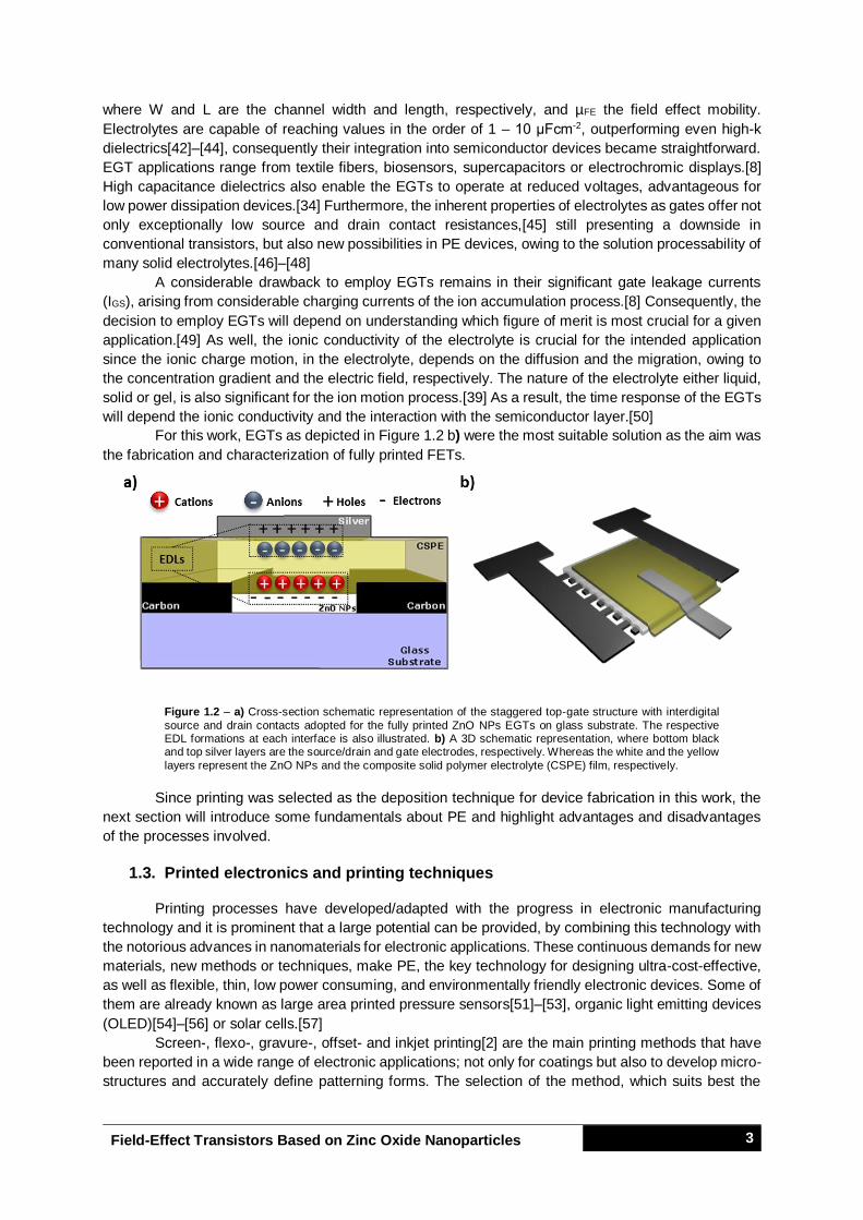
The use of electrolytes instead of a conventional dielectric layer in a FET results in an EGT.
One of the key features aimed for an electrolyte is the low electrical but high ionic conductivity (σ and
σi, respectively). This allows the electrolyte to behave as a pseudo dielectric, bridging the gap between
a conductive gate electrode and the channel region. By applying a VGS ions migrate in the electrolyte,
in this case in the composite solid polymer electrolyte (CSPE), accumulating at the respective interfaces,
forming electric double-layers (EDLs) as illustrated in Figure 1.2 a). The electric field at these EDLs
becomes very high and is capable of effectively inducing charges into the semiconductor.[39] This effect
can be used for transistor applications,[8] to investigate insulator-to-metal transitions[40] or
superconductivity behaviour of insulators.[41]
The evolution from conventional dielectric materials (oxides and nitrates) to electrolytes was
governed by the need for higher transistor driving currents, since it is directly proportional to the
capacitance of the dielectric layer per unit area (Ci), as we can see in equation 1.1:
𝐼𝐷 =𝑊𝜇𝐹𝐸𝐶𝑖
𝐿[(𝑉𝐺 − 𝑉𝑇 )𝑉𝐷 −
𝑉𝐷2
2] (Eq. 1.1)
Field-Effect Transistors Based on Zinc Oxide Nanoparticles 3
where W and L are the channel width and length, respectively, and µFE the field effect mobility.
Electrolytes are capable of reaching values in the order of 1 – 10 μFcm-2, outperforming even high-k
dielectrics[42]–[44], consequently their integration into semiconductor devices became straightforward.
EGT applications range from textile fibers, biosensors, supercapacitors or electrochromic displays.[8]
High capacitance dielectrics also enable the EGTs to operate at reduced voltages, advantageous for
low power dissipation devices.[34] Furthermore, the inherent properties of electrolytes as gates offer not
only exceptionally low source and drain contact resistances,[45] still presenting a downside in
conventional transistors, but also new possibilities in PE devices, owing to the solution processability of
many solid electrolytes.[46]–[48]
A considerable drawback to employ EGTs remains in their significant gate leakage currents
(IGS), arising from considerable charging currents of the ion accumulation process.[8] Consequently, the
decision to employ EGTs will depend on understanding which figure of merit is most crucial for a given
application.[49] As well, the ionic conductivity of the electrolyte is crucial for the intended application
since the ionic charge motion, in the electrolyte, depends on the diffusion and the migration, owing to
the concentration gradient and the electric field, respectively. The nature of the electrolyte either liquid,
solid or gel, is also significant for the ion motion process.[39] As a result, the time response of the EGTs
will depend the ionic conductivity and the interaction with the semiconductor layer.[50]
For this work, EGTs as depicted in Figure 1.2 b) were the most suitable solution as the aim was
the fabrication and characterization of fully printed FETs.
Figure 1.2 – a) Cross-section schematic representation of the staggered top-gate structure with interdigital
source and drain contacts adopted for the fully printed ZnO NPs EGTs on glass substrate. The respective EDL formations at each interface is also illustrated. b) A 3D schematic representation, where bottom black and top silver layers are the source/drain and gate electrodes, respectively. Whereas the white and the yellow
layers represent the ZnO NPs and the composite solid polymer electrolyte (CSPE) film, respectively.
Since printing was selected as the deposition technique for device fabrication in this work, the
next section will introduce some fundamentals about PE and highlight advantages and disadvantages
of the processes involved.
1.3. Printed electronics and printing techniques
Printing processes have developed/adapted with the progress in electronic manufacturing
technology and it is prominent that a large potential can be provided, by combining this technology with
the notorious advances in nanomaterials for electronic applications. These continuous demands for new
materials, new methods or techniques, make PE, the key technology for designing ultra-cost-effective,
as well as flexible, thin, low power consuming, and environmentally friendly electronic devices. Some of
them are already known as large area printed pressure sensors[51]–[53], organic light emitting devices
(OLED)[54]–[56] or solar cells.[57]
Screen-, flexo-, gravure-, offset- and inkjet printing[2] are the main printing methods that have
been reported in a wide range of electronic applications; not only for coatings but also to develop micro-
structures and accurately define patterning forms. The selection of the method, which suits best the
Field-Effect Transistors Based on Zinc Oxide Nanoparticles 4
intended application, depends on a number of properties, including the required printing quality, the
substrates, the inks and especially the resolution.
Printing techniques offer a variability of benefits against photolithography and vacuum
processes since they are fast, low-cost, offer fast prototyping, allow the reduction in material waste and
they enable the production of large area printing on flexible substrates by roll-to-roll (R2R) processes.
[58][59] Nevertheless, the resolution limits of the current printing techniques have an effect on the
performance of printed devices. In addition, as all printable materials are in solution form, their physical
and chemical stability, as well as viscosity, compatibility of the solvents and surface energies are the
major paradigms in choosing the suitable printing technique and evidently in the devices final
performance.[54][56]–[58]
It is desired to fabricate fully functional devices, using solely one printing technique instead of a
combination of the ones mentioned above, as this facilitates the fabrication process, leading to a more
cost-effective production. This approach was shown in recent scientific publications in a wide range of
applications: as patterning source and drain electrodes[62], or for all-printing stretchable electrochemical
devices.[63]
Therefore, in this thesis, screen-printing was chosen as the only fabrication technique to
produce the EGTs. Owing to the printed circuit board industry, it is the most versatile printing technique
and a quite mature technology for PE, in comparison to the ones mentioned before.[2] High aspect ratio
of printed objects is the most distinct feature of this technique. In addition, a wide range of thicknesses,
reaching from a few µm up to 100 µm can be achieved, which cannot be obtained by other printing
techniques.[64]
This technique is based on a screen mesh, which may be polyester or stainless steel, with a
defined printing pattern. This pattern is defined by photolithography of a light sensitive emulsion on the
mesh. A squeegee, of rubber or metal, moving over the screen, provides shear stress to the ink (or
printable paste), consequently decreasing its viscosity (viscoelasticity) and allowing it to cross through
the open areas onto the substrate. Solution viscosity, printing speed, angle and geometry of the
squeegee, mesh size, material, strength and snap-off (distance between screen and substrate) are the
main factors to consider in order to achieve high-resolution patterning (30 - 50 µm), through this printing
technique.[64] Viscosities, typically between 500 - 5000 cPs are referred to as desirable for this
technique, since inks with low viscosity will run through the mesh rather than dispensing out of it.[64] As
well, to obtain a high-resolution line width a compromise between surface energies, either of the
substrate or the ink, is required. Low surface energies of the substrate provides reduction of the
wettability of the printable paste, which leads to improved line resolutions. Moreover, as we can change
the wettability of the substrate, by controlling its surface energy, low viscosity inks can also be used to
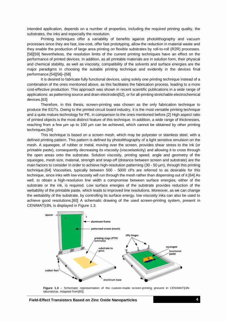
achieve good resolutions.[60] A schematic drawing of the used screen-printing system, present in
CENIMAT|i3N, is displayed in Figure 1.3.
Figure 1.3 – Schematic representation of the custom-made screen-printing present in CENIMAT|i3N laboratorys. Adapted from[65].

Field-Effect Transistors Based on Zinc Oxide Nanoparticles 5
Considering the required ink properties and their influence on the used printing technique the
next subsection will give a short overview of the ink preparation as well as some crucial remarks on its
composition.
1.3.1. Ink formulation and properties for thick films
The synthesis of a nanoparticle thick-film (thicknesses in micro scale) ink must be made by a
careful selection of the raw materials, so that its characteristics do not compromise the intended
application. The ink must be prepared dispersing the desired inorganic powders/precursors in a viscous
liquid, the vehicle, which is responsible for the deposition of the powder onto the substrate. Both of these
components must be dispersed along with an organic or sacrificial binder with a solvent and a wetting
agent. For this, resin or polymeric binders such as cellulosic polymers, as is the case of ethyl cellulose
(EC) is widely used for industrial screen-printing as it provides good printing and levelling.[66] The
sacrificial binder is used in order to hold the inorganic powders together and give the ink the intended
rheological properties.[67] Additionally, solvents with low vapour pressure at room temperature and a
high vapour pressure at 100 – 150 °C, should be selected, in order to prevent ink drying by evaporation
on the screen and enable rapid drying of the printed parts by annealing.
Thereby, to obtain the mechanical and electrical required properties, which are given by the
powder, the vehicle must be eliminated (“burned-out”), so there will be no trace of it in the final film.
Nevertheless, the properties of the thick-film are not just influenced by the bulk properties of the
inorganic powders, but also by their surface area, particle size, tap density, purity and interface quality.
For instance, surface area influence viscosity, particle size and their dispersion effect, which in turn has
an effect on ink behaviour, film surface smoothness, film conductivity, film density, printing and its
adhesion to the substrate.[68] Due to the presence of agglomerates, large interface roughness between
the transistor channel and the gate insulator can occur, forming charge traps, which makes the charge
transfer between source and drain electrodes difficult. Consequently, the turn-on voltage (VOn) and the
subthreshold swing (Ss) of the devices can be impaired. One way of overcoming this problem is to
stabilize the nanodispersions with surfactants.[5] However, the presence of the vehicle, as well as
surfactants or additives decline the electrical performance of the thick-film, likewise the type of substrate
that can be used, since high temperatures or UV irradiation is needed to burn them out.[5][65]
1.4. Inorganic field-effect transistors on paper
Paper electronics appears as a new area of technology, which has begun to show that it is
possible to counteract all the issues related to a decrease in waste material, making technology cheaper,
disposable and eco-friendly, even if this new approach is on an early stage of development.
Furthermore, paper is also recyclable, lightweight and widely used as a flexible substrate in everyday
life. Additionally and most importantly manufacturing process can exceed 100 kmh-1, making it cheap (≈
0.1 cent dm-2) compared to other substrates used in electronics, like for instance polyethylene
terephthalate (PET ≈ 2 cent dm-2).[9]
The first step in the application of paper as a substrate in electronics, was given in 1968[31],
having today several applications of it as substrate for sensors, solar cells, gas sensors or displays.
Nonetheless, many efforts have been made to make it more functional beyond a simple substrate.[69]
Fortunato et al. have shown for the first time (see Figure 1.4 a)), using this remarkable material, that in
addition to the substrate, it can also work as an active part i.e. dielectric in FETs.[11] The benefit of
being applied as dielectric is related to its foam-like structure that enables moisture retention, which
produces a large gate capacitance at low frequencies due to the free charges.[70]
This technological leap made their application in memory transistors[14] and CMOS devices[15]
possible. Recent studies also confirm that the properties of the paper-based transistors are affected by
the structure, fiber type and thickness of the paper.[12][13]
Taking these approaches into account another possibility will be explored using, once again,
ZnO NPs as the functional semiconducting layer. However, instead of using physical vapour deposition
(PVD) techniques, the sol-gel method proposed by Jaber and Laânab[30] will be used. Consequently,

Field-Effect Transistors Based on Zinc Oxide Nanoparticles 6
it will be possible to coat the cellulose fibers of the paper substrate with ZnO nanoparticles under ambient
atmosphere at room temperature. Thus, to build an interstate structure (similar to the one in Figure 1.4
b)), where this time paper can play three different roles: substrate, dielectric and semiconductor after
being functionalized, is feasible.
Figure 1.4 – a) An image of the developed FETs in CENIMAT|i3N where paper was applied as substrate and
dielectric and b) its schematic representation. Adapted from[13].

Field-Effect Transistors Based on Zinc Oxide Nanoparticles 7
2. MATERIALS AND METHODS: FABRICATION, OPTIMIZATION AND CHARACTERIZATION PROCESS OF EGTs and FETs
This chapter aims to present all the steps that were taken for the production and characterization
of EGTs on glass and FETs on paper. First, the formulation of the semiconductor layer will be presented,
which in case of EGTs is a printable paste, containing a dispersion of ZnO nanoparticles in a sacrificial
binder EC. In case of the paper ZnO NPs FETs, paper was coated with ZnO NPs by sol-gel method, in
an aqueous solution of zinc acetate dihydrate and sodium hydroxide.
Secondly, the architecture chosen for each transistor type will be displayed as well as the steps
and techniques that were used for all the layer depositions.
Finally, all the characterization techniques selected to study the morphology, structure and
stability of the semiconductor and electrolyte layers will be listed. In the end it will be shown how the
electrical characterization of the final devices was conducted.
2.1. ZnO NPs ink formulation materials and reagents
The methods used for preparing ZnO NPs screen-printing paste were based and adapted from
the literature.[71] First, the vehicle was prepared by dissolving 5 %wt Ethyl Cellulose 300 cP (C6H7O2
(OC2H5)3; CAS: 9004-57-3) from Aldrich on an 80:20 toluene/ethanol solution (C6H5CH3; CAS: 108-88-
3/ C2H6O; CAS: 64-17-5). After complete dissolution, which takes around 12 hours under stirring at 600
rpm, 0.25, 0.5, 0.75 and 1 g of ZnO nanopowder, <100 nm particle size (CAS: 1314-13-2) from Aldrich
were added always in the same amount of vehicle. The solutions should be kept under continuous
stirring until their complete dispersion.
2.2. ZnO semiconductor layer by sol-gel method
As mentioned in section 1.4 and taking into account the work done by Jaber and Laânab[30] a
piece of Felix Schoeller raw (FSR) paper, was submersed in an aqueous solution. For that, 4 cm2 of
FSR, which consist of pressed cellulose fibers with high porosity and 141 µm of thickness, obtained
from Felix Schoeller with, was covered on one side by adhesive kapton tape. The solution was prepared
by mixing 1.757 g of zinc acetate dihydrate (CAS : 5970-45-6, ZnC4H6O4·2H2O, MW: 219.51) from
Sigma-Aldrich and 0.796 g sodium hydroxide (NaOH), previously dissolved in 100 ml and 20 ml of
deionized water, respectively. Firstly, the paper must be immersed in the zinc acetate solution and then
NaOH at a rate of 2 ml/min was added. While adding NaOH, the stirring should increase to 1300 rpm
and be maintained for 1h. Finally, the paper was washed with deionized water to remove excess and
left drying in air. It is necessary to supervise the process because the paper can glue up the edges of
the beaker and can get stuck due to the stirrer.
2.3. Fabrication and optimization of the ZnO NPs EGTs and paper ZnO NPs FETs
2.3.1. ZnO NPs EGTs by screen-printing
In case of ZnO NPs EGTs, a staggered top-gate architecture was adopted. Since ZnO NPs are
intended to be used as semiconductor layer, two considerations were made relatively to source and
drain (S/D) electrodes. First, ITO interdigital S/D electrodes were pattern via photolithography, as
illustrated in Figure 2.1, and carbon interdigital S/D electrodes by screen-printing as illustrated in Figure
2.2. Also, in this last figure is briefly described all the printing steps that were taken for achieved the
fully-printed devices. Nevertheless, in Annex A, a more detailed description of the all steps for the EGTs
development can be found.

Field-Effect Transistors Based on Zinc Oxide Nanoparticles 8
Figure 2.1 – Schematic representation of the ITO interdigital S/D electrodes patterned via photolithography.
Figure 2.2 – Schematic representation of the developed fully-printed ZnO NPs EGTs.
2.3.2. Paper ZnO NPs FETs
As mentioned in 2.2 the first step consisted in growing ZnO nanoparticles on the cellulose fibers
on the surface of FSR paper, which was itself used as a dielectric for the intended devices. Figure 2.3
displays a simple schematic representation, of the steps that were taken in order to achieve a staggered
bottom-gate architecture, for the paper ZnO NPs FETs. Nevertheless, in Annex A a more detailed
description of the whole fabrication is shown.
Figure 2.3 - Schematic representation of the developed paper ZnO NPs FETs.
2.4. Characterization techniques
Several techniques were used in order to characterize the various layers of the transistors. The
rheological behaviour of the ZnO ink and the lithium-based polymer electrolyte was evaluated using
Bohlin Gemini HRNANO rotational rheometer, with parallel plates geometry (20 mm diameter and 500 µm
gap) for steady-state measurements. Temperature was kept at 25 °C and, before starting the
measurements, samples were subjected to a pre-shearing stage, with a pre-shear of 1 s−1 applied for

Field-Effect Transistors Based on Zinc Oxide Nanoparticles 9
30 s, followed by an equilibration time of 180 s. A solvent trap was used in order to avoid evaporation.
The steady-state measurements were performed for shear rates up to 1000 s−1.
Atomic force microscopy (AFM) was performed in non-contact mode using an Asylum MFP-3D
instrument. The resolution of the image was 512 lines by 512 columns and the scan size was 5×5 μm2
and 20×20 µm2.
Both semiconductor layers were characterized by SEM-FIB using a Carl Zeiss AURIGA
CrossBeam workstation instrument. As well as the crystallinity and structure of the samples were
obtained by X-Ray Diffraction (XRD, PANalytical, model X’Pert Pro), in Bragg-Brentano geometry with
Cu Kα line radiation (λ=1.5406 Å) at 45 KV and 40 mA. Particularly, in the case of ZnO screen-printed
films XRD analysis was performed first at 30 °C and subsequently between 100 °C and 500 °C, with a
step of 50 °C.
Fourier transform Infrared (FTIR) spectroscopy was applied in order to evaluate the EC, toluene
and ethanol thermal degradation. The ZnO ink was screen-printed on glass substrates, previously
cleaned in acetone, IPA and DI water and then exposed to different annealing temperatures, ranging
from 100 °C to 450 °C, with a step of 50 °C, on a hotplate. The spectra were acquired between 4500-
500 cm-1 by a Nicolet 6700 FTIR Thermo Electron Corporation device. In addition, with the same
purpose of understanding the thermal degradation of the ink constituents, thermogravimetric and
differential scanning calorimetry (TG-DSC) measurements were carried out on the semiconductor ink
solution with a Simultaneous Thermal Analyzer (TG-DSC - STA 449 F3 Jupiter). Approximately 20 mg
of each sample was loaded into an open Al crucible and heated from room temperature to 550 °C with
a heating rate of 5 °Cmin-1, in ambient conditions.
Electrochemical Impedance Spectroscopy (EIS) was done using Gamry Instruments Reference
600 Potentiostat in order to determine:
The capacitance-frequency dependency of the lithium-based polymer electrolyte samples
inserted between stainless steel discs with an area of 1.039 cm2 (see Figure 3.8 a)). The results
were acquired in a frequency range of 1 MHz to 100 mHz with 25 mV as ac excitation voltage
at 1 V dc.
The capacitance-frequency dependency of FSR paper, using gold discs with an area of 1.77
cm2 and in a frequency range of 1 MHz to 10 mHz with 5 mV as ac excitation voltage.
Previously, both sides of the paper were coated with about 120 nm of aluminium by e-beam
evaporation, in order to improve the electrical contact between the paper and the gold discs.
The impedance spectroscopy of the ZnO thick films was evaluated in a frequency range of 1
MHz to 10 mHz with 25 mV as ac excitation voltage. For that, step number 2 and 3 of the Annex
A were followed, but a wider range of temperatures was established, including room
temperature, 100 °C and from 200 to 400 °C, with a step size of 50 °C.
The electrochemical response of lithium-based polymer electrolyte and the combination with
annealed ZnO ink was evaluated by cyclic voltammetry (CV) through a Gamry Instruments Reference
600 Potentiostat. Doctor blade technique was used in order to deposit both layers, on stainless steel
discs. In the case of the electrolyte, the layer was exposed, first to UV radiation during 5 min and,
afterwards, dried on a hotplate at 70 °C. On the other hand, the ZnO thick-film was annealed, during
30 min at 350 °C. All films were electrochemically cycled from 4 to -4 V, at a scan rate of 10 mVs-1.
Furthermore, the Olympus BX51 microscope, and the software Cell A were used to measure the
transistors’ dimensions. In particular, the semiconductor channel lengths and widths were measured
using a Leica IC80 HD microscope and the LAS V4.3 software.
Electrical measurements of the resistivity of carbon and silver electrodes were performed using
the four-point probe technique (Jandel Enginneering Ltd) and the thickness of the screen-printed films
were measured with an Ambios XP-Plus 200 Stylus profilometer.
The electrical characterization of both of the transistor types was performed in the dark at room
temperature using an Agilent 4155C semiconductor parameter analyser connected to a Cascade
Microtech M150 manual microprobe station, controlled by the software Metrics ICS.

Field-Effect Transistors Based on Zinc Oxide Nanoparticles 10

Field-Effect Transistors Based on Zinc Oxide Nanoparticles 11
3. RESULTS AND DISCUSSION
3.1. Characterization and properties of ZnO NPs ink semiconducting layer
In this section, the focus will be on the development and characterization of both of the
semiconductor and the electrolyte layers. As was already mentioned before, screen-printing depends
highly on the used inks and their non-newtonian behaviour during the deposition process. Consequently,
rheological measurements were performed on the used functional inks (ZnO and electrolyte).
After verifying a good dispersion of the powder and the viscous character of the solutions listed in section
2.1, thick films of ZnO NPs were printed on glass substrates, using a mesh model 77-55 (mesh count
190, aperture 81 µm thread diameter 55 µm).
After visual and microscope inspection, the solution with 1 g of ZnO powder resulted in best
uniformity, compactness and adhesion, where films with an average thickness of 1.39 µm were
achieved. Therefore, this was the ink employed and characterized as the semiconducting layer.
After deposition, the vehicle’s response to high temperature during the burn-out process will be
investigated by TG-DSC, as this determines the necessary temperature at which the film should be
subjected in order to retain solely its semiconductor content. The films will then go through a number of
characterization steps to further investigate their structural and morphological properties (FTIR, SEM,
and XRD) in respect to the applied annealing temperatures.
3.1.1. Rheological measurements
The rheology of the ink is strongly dependent on the rheology of the vehicle since sacrificial
binder and solvent are the main components for screen-printing inks. It is also pertinent to preserve
good printability during the time it remains on the screen and the printing parameters must allow for high
yield. Thus, the variation of the steady-state viscosity as a function of the shear rate was performed for
ZnO NPs ink, vehicle and lithium-based polymer electrolyte, as shown in Figure 3.1.
Figure 3.1 – Viscosity as function of the sear rate for ZnO NPs Ink, vehicle (EC 5 wt% on toluene/ethanol)
and lithium- based polymer electrolyte.
First, a decrease of the viscosity with increasing shear rate is noted, especially for vehicle and
electrolyte, which is related with their viscoelastic properties, allowing them to cross through the screen
open areas onto the substrate.
In the case of ZnO NPs ink it is possible to say the viscosity is practically independent of the
shear rate applied. Furthermore, the addition of ZnO nanoparticles decreases the viscosity of the
vehicle, particularly of the EC since it is a polymer working as a sacrificial binder. This fact is expected
as a result of the presence of nanostructures inside a polymer nanocomposite (PNC), which can modify
its structural, dynamical and viscous behaviour. These changes are arising not only from the high
surface-area-to-volume ratio of the nanoparticles but also due to the strong polymer-nanoparticles
0.1 1 10 100 100010
2
103
104
105
106
ZnO NPs Ink Vehicle
Electrolyte
Shear Rate (s-1
)
Vis
co
sit
y (
cP
)
Field-Effect Transistors Based on Zinc Oxide Nanoparticles 12
interactions, which affect the entanglement of the EC chains.[72] Also, It is possible to affirm that ZnO
NPs ink shows a newtonian flow for the applied shear rate range, since there is no significant change in
its viscosity during the measurement, except for 100 s-1, where only a slight change was verified. This
indicates that the printed semiconducting films are less affected by printing parameters such as the
applied force or velocity during the deposition. Consequently, reproduction of the films are favoured
even when altering the deposition parameters, which happens when doing it by hand in a non-automated
way. Nevertheless, it is necessary to take heed, since inks with low viscosities can pass through the
mesh without the application of any shear stress. Furthermore, the formulated semiconducting ink shows
good printability, good adhesion to the glass substrate and high uniformity which are crucial properties
for instance for high interface quality and improved yield of the final EGT devices. Additionally, the ink
was easily removed from the screen during the clean-up process with EtOH, which is desirable
especially on an industrial scale with online R2R processes.
In contrast, the electrolyte exhibits mostly a non-newtonian behaviour. Furthermore, the fact
that its dynamic viscosity is high becomes a problem when printed through the mesh, since the ink is
blocked and it gets difficult to obtain a uniform printing pattern. This resulted in non-uniform films with
defects, affecting the semiconductors coverage and consequently the performance of the devices. An
illustration of the screen-printed electrolyte film on glass substrate can be accessed in Annex B. It might
suggests that in order to achieve an improved printed layer a better control under the applied shear rate
should be done. Through the homemade screen-printing it could be quite challenging; however, via an
automatic one a better understanding of the phenomenon might be possible. As a result, snap-off, shear
rate, angle, geometry and squeegee type could be investigated in the printed layers reproducibility.
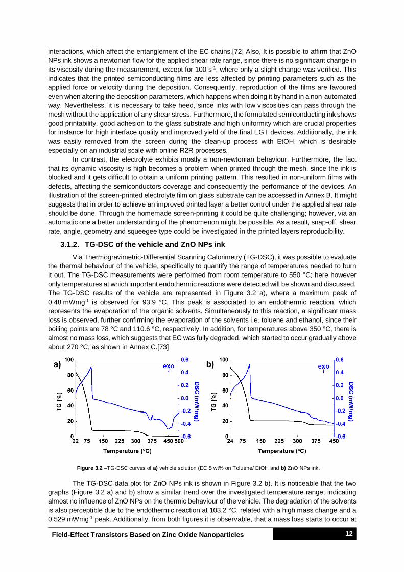
3.1.2. TG-DSC of the vehicle and ZnO NPs ink
Via Thermogravimetric-Differential Scanning Calorimetry (TG-DSC), it was possible to evaluate
the thermal behaviour of the vehicle, specifically to quantify the range of temperatures needed to burn
it out. The TG-DSC measurements were performed from room temperature to 550 °C; here however
only temperatures at which important endothermic reactions were detected will be shown and discussed.
The TG-DSC results of the vehicle are represented in Figure 3.2 a), where a maximum peak of
0.48 mWmg-1 is observed for 93.9 °C. This peak is associated to an endothermic reaction, which
represents the evaporation of the organic solvents. Simultaneously to this reaction, a significant mass
loss is observed, further confirming the evaporation of the solvents i.e. toluene and ethanol, since their
boiling points are 78 °C and 110.6 °C, respectively. In addition, for temperatures above 350 °C, there is
almost no mass loss, which suggests that EC was fully degraded, which started to occur gradually above
about 270 °C, as shown in Annex C.[73]
Figure 3.2 –TG-DSC curves of a) vehicle solution (EC 5 wt% on Toluene/ EtOH and b) ZnO NPs ink.
The TG-DSC data plot for ZnO NPs ink is shown in Figure 3.2 b). It is noticeable that the two
graphs (Figure 3.2 a) and b) show a similar trend over the investigated temperature range, indicating
almost no influence of ZnO NPs on the thermic behaviour of the vehicle. The degradation of the solvents
is also perceptible due to the endothermic reaction at 103.2 °C, related with a high mass change and a
0.529 mWmg-1 peak. Additionally, from both figures it is observable, that a mass loss starts to occur at

Field-Effect Transistors Based on Zinc Oxide Nanoparticles 13
room temperature, which is associated to the low flash points of both solvents, 12 and 14 °C for ethanol
and toluene, respectively. Once again, for temperatures above 270 °C degradation of EC, owing to the
associated mass loss, is suggested. On the other hand, above 400 °C, there still is ZnO powder present
in the crucible, since TG-DSC data still shows a linear positive mass value. This is not the case for the
pure vehicle solution, reaching 0 % of initial mass for the final temperature. This observation indicates
a 100 % thermal degradation of the vehicle; the desired effect of the burn-out process. Combining the
knowledge of the individual measurements leads to the assumption that an annealing step above 300 ºC
of a screen-printed ZnO NPs thick film would lead to a pure ZnO NPs film, which can then be used as
the functional semiconducting layer in an EGT.
The next subsection will focus on the burn out process but this time on ZnO NPs ink screen-
printed on glass substrates. The idea is to verify through the Attenuated Total Reflectance-Fourier
Transform Infrared Spectroscopy (ATR-FTIR), if thick films exhibit the same behaviour in relation to the
increase in temperature, as in the previous subsection concerning their ink form.
3.1.3. ATR-FTIR of the ZnO NPs ink
The study of the thermal decomposition of the vehicle, namely the EC content was studied also
by ATR-FTIR. The semiconductor ink was screen-printed on glass substrates and annealed at different
temperatures. In Annex DAnnex an ATR-FTIR spectrum of the compounds in solution form is also
shown. Figure 3.3 shows the FTIR spectra for 24 °C, 300 °C and 450 °C. For EC, the peak at 3500 cm- 1
represents the stretching of O-H groups both in the closed ring structure and in intra/intermolecular
hydrogen bonds. The peaks around 2980-2870 cm-1 may indicate CH stretching and the distinct peak
at 1375 cm-1 refers to CH3 bending. Additionally, the small peak at 1440 cm-1 represents CH2 bending,
and the broad peak around 1100 cm-1 may be due to C-O-C stretching in the cyclic ether.[74]
Figure 3.3 - ATR-FTIR spectra of the ZnO NPs ink after being screen-printed and annealeted at 24, 300 and 450 °C.
Annex E provides a better understanding of the temperature effect on the screen-printed films.
At 100 °C, there are signs of thermal degradation of the ink, since there is a decrease of the absorbance
peaks, however quite small. The spectra for 150 °C and 200 °C remain virtually the same, though, the
spectrum for 250 °C shows a clear reduction of the absorbance peaks mentioned above, indicating the
beginning of EC thermal decomposition. The absorbance peaks for EC have almost disappeared for
300 °C and finally, from 350 °C to 450 °C, there are no absorbance peaks corresponding to EC, meaning
that the polymer has been degraded.
In addition to this, a notable loss of adhesion of the films to the substrates was identified after
annealing, especially for those with annealing temperatures above 300 °C. This detail is expected since
EC works as a binder (improves adhesion), which is lost after application of the burn-out temperatures
4000 3500 3000 1500 1000
C-O-C
Stretch
C-H
Bend
C-H
Stretch
24 C 300 C 450 C
Wavenumber (cm-1)
Inte
ns
ity
(a
.u.)
O-H
Stretch

Field-Effect Transistors Based on Zinc Oxide Nanoparticles 14
determined by TG-DSC and ATR-FTIR. Later, in subsection 3.7.2, the influence of these temperatures
on the performance of the EGTs will be discussed.
3.1.4. Structural and morphological analysis of ZnO NPs ink
SEM analysis was carried out with the purpose to explore the shape, morphology and size of
the commercial ZnO NPs in the ink. Figure 3.4 a) shows the top surface of the printed thick film
performed at room temperature. In spite of seeing some agglomerates and roughness, the printed film
exhibits a good coverage of the glass substrate, resulting in good film uniformity.
Figure 3.4 – a) The topographical view, obtained by SEM, of the top surface and XRD diffractogram, at 30, 300, 350 and 500 °C, of ZnO NPs Ink, b) SEM picture of the ZnO NPs dispersed in ink, and c) the
corresponding 3D view of the top surface, with an area of 25 µm2 acquired by AFM.
X-Ray Diffraction (XRD) at different annealing temperatures was also performed on the screen-
printed films in order to verify whether the nanostructures remained stable with increasing temperatures.
The inset of Figure 3.4 a) shows XRD diffractograms after annealing at 30, 300, 350 and 500 °C. The
diffraction peaks match to ZnO with hexagonal symmetry and wurtzite structure (lattice constants a =
3.24982 Å and c = 5.20661 Å) according to ICDD 00-036-1451. There are no significant changes as
temperature increases, and the crystallite size determined by the Scherrer method between 100 and
400 °C remains around 73 and 76 nm, respectively, as depicted in Annex F.
From Figure 3.4 b) it is possible to observe not only nanostructures, but also that several particle
morphologies are present, namely nanospheroids, nanorods and nanosheets. Clearly, there is not an
uniform distribution, neither in shape nor in size of the nanostructures, and numerous aggregates are
visible. Still, the way how these different morphologies are organized will provide a good contribution for
the semiconducting layer, since a continuous path between them is required for electrical conduction. It
was also verified through SEM images that with increasing temperature no visible changes in the
nanostructures occur.
The presence of EC is not distinguishable from the SEM images, which is related to the high
amount of added ZnO NPs that mask it. Nonetheless, in Annex G an image of the vehicle, which also
contains EC, is shown. XRD was also performed on the EC powder and the related diffractogram is
depicted in Annex H. In the same annex, the comparison between EC powder and ZnO NPs ink
annealed at different temperatures was made. The respective diffractograms revealed that owing to the
low amount of the cellulose derivate in the ink it is challenging to obtain a conclusion about the effect of
the temperature on the same through the XRD data.
Figure 3.4 c) shows the 3D view of the surface, obtained by AFM, which exhibit an average rms
surface roughness of 115.1 nm. This value is associated to the presence of agglomerates, which means
that the ZnO NPs are not well dispersed in the vehicle. An alternative suggested to overcome this
problem in future developments can be the use of surfactants in order stabilize the nanostructures or
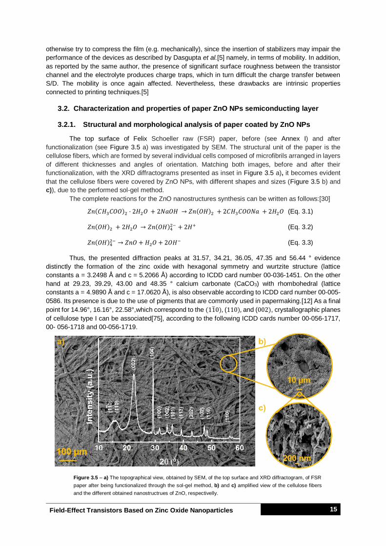
Field-Effect Transistors Based on Zinc Oxide Nanoparticles 15
otherwise try to compress the film (e.g. mechanically), since the insertion of stabilizers may impair the
performance of the devices as described by Dasgupta et al.[5] namely, in terms of mobility. In addition,
as reported by the same author, the presence of significant surface roughness between the transistor
channel and the electrolyte produces charge traps, which in turn difficult the charge transfer between
S/D. The mobility is once again affected. Nevertheless, these drawbacks are intrinsic properties
connected to printing techniques.[5]
3.2. Characterization and properties of paper ZnO NPs semiconducting layer
3.2.1. Structural and morphological analysis of paper coated by ZnO NPs
The top surface of Felix Schoeller raw (FSR) paper, before (see Annex I) and after
functionalization (see Figure 3.5 a) was investigated by SEM. The structural unit of the paper is the
cellulose fibers, which are formed by several individual cells composed of microfibrils arranged in layers
of different thicknesses and angles of orientation. Matching both images, before and after their
functionalization, with the XRD diffractograms presented as inset in Figure 3.5 a), it becomes evident
that the cellulose fibers were covered by ZnO NPs, with different shapes and sizes (Figure 3.5 b) and
c)), due to the performed sol-gel method.
The complete reactions for the ZnO nanostructures synthesis can be written as follows:[30]
𝑍𝑛(𝐶𝐻3𝐶𝑂𝑂)2 · 2𝐻2𝑂 + 2𝑁𝑎𝑂𝐻 → 𝑍𝑛(𝑂𝐻)2 + 2𝐶𝐻3𝐶𝑂𝑂𝑁𝑎 + 2𝐻2𝑂 (Eq. 3.1)
𝑍𝑛(𝑂𝐻)2 + 2𝐻2𝑂 → 𝑍𝑛(𝑂𝐻)42− + 2𝐻+ (Eq. 3.2)
𝑍𝑛(𝑂𝐻)42− → 𝑍𝑛𝑂 + 𝐻2𝑂 + 2𝑂𝐻− (Eq. 3.3)
Thus, the presented diffraction peaks at 31.57, 34.21, 36.05, 47.35 and 56.44 ° evidence
distinctly the formation of the zinc oxide with hexagonal symmetry and wurtzite structure (lattice
constants a = 3.2498 Å and c = 5.2066 Å) according to ICDD card number 00-036-1451. On the other
hand at 29.23, 39.29, 43.00 and 48.35 ° calcium carbonate (CaCO3) with rhombohedral (lattice
constants a = 4.9890 Å and c = 17.0620 Å), is also observable according to ICDD card number 00-005-
0586. Its presence is due to the use of pigments that are commonly used in papermaking.[12] As a final
point for 14.96°, 16.16°, 22.58°,which correspond to the (11̅0), (110), and (002), crystallographic planes
of cellulose type I can be associated[75], according to the following ICDD cards number 00-056-1717,
00- 056-1718 and 00-056-1719.
Figure 3.5 – a) The topographical view, obtained by SEM, of the top surface and XRD diffractogram, of FSR
paper after being functionalized through the sol-gel method, b) and c) amplified view of the cellulose fibers
and the different obtained nanostructrues of ZnO, respectivelly.

Field-Effect Transistors Based on Zinc Oxide Nanoparticles 16
As a result, FSR is suitable for its integration into FETs, since its top surface is reasonably well
covered with ZnO, taking once again the role of the semiconductor. Due to the excellent coverage,
continuous conductive paths between S and D will be possible, even for higher L. Moreover this coating
processes has been done at room temperature and in lab conditions without the requirement of
sputtering processes, as reported in the literature.[12]
3.2.2. FTIR of the paper coated by ZnO NPs
The ATR-FTIR spectra of the FSR paper, Figure 3.6 b), before and after its surface being
functionalized with ZnO nanoparticles is shown in Figure 3.6 a). It is evident, that both spectrums present
the same cellulose characteristic peaks namely O-H, C-H and C-O stretching vibrations at
3600- 3000 cm-1, 2900 cm-1 and 1060 cm-1, respectively. Another peak at 1640 cm-1 is also observable
and is linked with O-H bending vibration of absorbed water molecules.[12] It is also perceptible, that
when the paper is functionalized that a decrease in the intensity of the absorbance peaks is detected. It
is known that the most intense peak is the highest amount of material present in the specimen. In this
case, it suggests that the number of cellulosic fibers remain the same, but since its surface has been
functionalized with ZnO, a lower interaction between the IR beam and the cellulose fibers is possible.[76]
This indicates that a layer with a considerable thickness and good coverage of the top surface of the
paper was achieved, which has been confirmed previously by structural and morphological analyses.
Figure 3.6 – a) ATR-FTIR spectra of the Felix Schoeller raw (FSR) paper before and after functionalization with ZnO NPs through the sol-gel method and b) a piece of FSR paper without and with adhesive kapton tape covering one side.
3.3. Characterization and properties of lithium based polymer electrolyte
A combination of succinonitrile (Aldrich), acrylic resin (TB 3003 K, ThreeBond), lithium
perchlorate (LiClO4, Sigma-Aldrich) and titanium dioxide (TiO2) nanoparticles (Rockwood) was used to
form a composite solid polymer electrolyte (CSPE), namely a lithium-based polymer electrolyte, in order
to be implemented in the EGTs. This type of electrolytes are a good approach for the intended devices
fabrication, since it can be printed and thereby will provide fully printed ZnO NPs EGTs, as will be
demonstrated later. On the other hand, solid electrolytes are desirable as an alternative to liquid ones
for EGTs, as poor mechanical properties, problems with its application (fabrication and devices
architecture), safety and resistance to aggressive environments can be minimized or solved.[77]
Furthermore, polymer electrolytes have recently been used in applications such as electrochromic
displays, thin-film batteries, fuel cells and supercapacitors, showing their versatility.[39]
This lithium-based polymer electrolyte has been developed in CENIMAT|i3N, it has however not
yet been fully characterized for the intended application. A rheological characterization has been made
in subsection 3.1.1 and it was found, that it behaves as a non-newtonian fluid, (a requirement for screen-
printing), achieving a layer thickness of 18.43 µm, only with one printing step, and an average rms
surface roughness of 261 nm. Figure 3.7 displays the 3D topographic view of the electrolyte surface
provided by AFM.
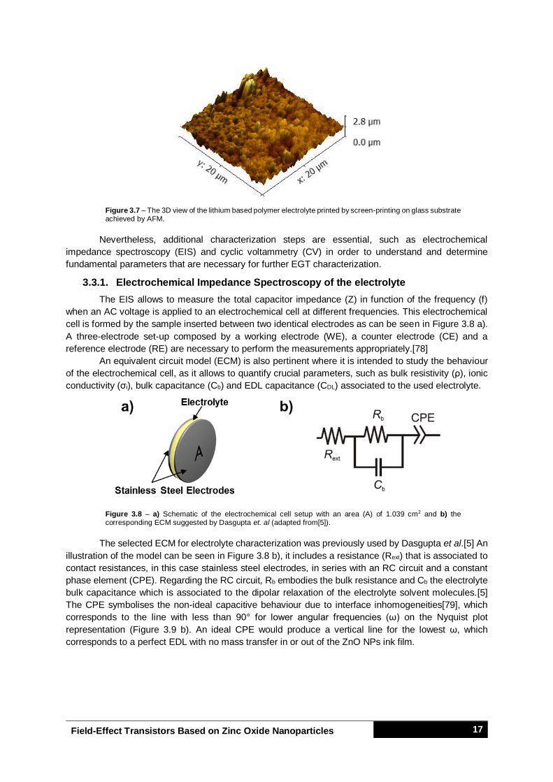
Field-Effect Transistors Based on Zinc Oxide Nanoparticles 17
Figure 3.7 – The 3D view of the lithium based polymer electrolyte printed by screen-printing on glass substrate achieved by AFM.
Nevertheless, additional characterization steps are essential, such as electrochemical
impedance spectroscopy (EIS) and cyclic voltammetry (CV) in order to understand and determine
fundamental parameters that are necessary for further EGT characterization.
3.3.1. Electrochemical Impedance Spectroscopy of the electrolyte
The EIS allows to measure the total capacitor impedance (Z) in function of the frequency (f)
when an AC voltage is applied to an electrochemical cell at different frequencies. This electrochemical
cell is formed by the sample inserted between two identical electrodes as can be seen in Figure 3.8 a).
A three-electrode set-up composed by a working electrode (WE), a counter electrode (CE) and a
reference electrode (RE) are necessary to perform the measurements appropriately.[78]
An equivalent circuit model (ECM) is also pertinent where it is intended to study the behaviour
of the electrochemical cell, as it allows to quantify crucial parameters, such as bulk resistivity (ρ), ionic
conductivity (σi), bulk capacitance (Cb) and EDL capacitance (CDL) associated to the used electrolyte.
Figure 3.8 – a) Schematic of the electrochemical cell setup with an area (A) of 1.039 cm2 and b) the corresponding ECM suggested by Dasgupta et. al (adapted from[5]).
The selected ECM for electrolyte characterization was previously used by Dasgupta et al.[5] An
illustration of the model can be seen in Figure 3.8 b), it includes a resistance (Rext) that is associated to
contact resistances, in this case stainless steel electrodes, in series with an RC circuit and a constant
phase element (CPE). Regarding the RC circuit, Rb embodies the bulk resistance and Cb the electrolyte
bulk capacitance which is associated to the dipolar relaxation of the electrolyte solvent molecules.[5]
The CPE symbolises the non-ideal capacitive behaviour due to interface inhomogeneities[79], which
corresponds to the line with less than 90° for lower angular frequencies (ω) on the Nyquist plot
representation (Figure 3.9 b). An ideal CPE would produce a vertical line for the lowest ω, which
corresponds to a perfect EDL with no mass transfer in or out of the ZnO NPs ink film.

Field-Effect Transistors Based on Zinc Oxide Nanoparticles 18
Figure 3.9 – a) The measured effective capacitance and phases (circles) and the ECM fited curves (lines) and b) the respective nyquist plot of the lithium-based polymer electrolyte.
The data and the fitting provided by the ECM is depicted in Figure 3.9. Firstly, the chosen ECM
fits reasonably well the entire frequency spectrum as can be verified for both of the Nyquist Figure 3.9
b) and total impedance graph Annex J. In addition, two domains can be distinguished in Figure 3.9 a)
since an electrochemical cell can have a capacitive (for θ < - 45°) or a resistive (θ > - 45°) behaviour.
Accordantly, for frequencies less than 24 Hz a capacitive domain is verified, which is characterized by
a high capacitance from the EDL formation. On the other hand, above this value, ionic relaxation
provides a resistive behaviour.[39]
Jovi´c et al.[80] have proposed a model for CDL calculation as can be shown in equation 3.4.
𝐶𝐷𝐿 = [𝑌0𝑅𝑒𝑥𝑡− (𝛼−1)]
1𝛼⁄ (Eq. 3.4)
In equation number 3.4 Y0 is linked to the capacitance of the CPE, and α is a constant (between
0 and 1) related to the CPE, dictating how non-ideally it behaves. Nevertheless, due to surface
roughness and non-uniform current distribution, certain theories refer that α must be treated as an
empirical constant with no real physical basis.[81]
Still, in the present work and as reported by Dasgupta et al.[5] and Santos et al.[7] the results
were determinate merging the selected ECM with the equation 3.4, and CDL of the electrolyte gives
2.57 × 10⁻⁶ 𝐹, with an Y0 of 2.15 × 10⁻⁵ 𝑆𝑠𝛼, Rext equal to 117.2 𝛺, α equal to 7.38 × 10⁻¹ and with the
cells area of 1.039 𝑐𝑚2, CDL per area corresponds to 2.47 × 10⁻⁶ 𝐹𝑐𝑚−2. Regarding the measured
effective capacitance, Ceff, in Figure 3.9 a), the real value is slightly higher than the value determined
which also depends on the Cb of the electrolyte. However, it is necessary to note that countless factors
are involved, such as the cell setup and dimensions, or even the ECM fitting parameters, which also
have an associated error (Annex K). Nevertheless, the determined value for CDL lies in the standard
range for the use of electrolytes in EGTs, i.e. 1-10 µFcm-2, as described by Kim et al.[8]
The bulk resistance of the electrolyte (Rb) was determined, using the ECM fit, as 513.3 Ω.
Consequently the ionic conductivity (σi) of the electrolyte was determined as 3.09 × 10⁻⁷ 𝑆𝑐𝑚−1, using
the accepted equation.[7] The ionic conductivity of the lithium-based polymer electrolyte remains in
agreement to the reported range for polymer electrolytes which lies between 10−8 and 10−4 𝑆𝑐𝑚−1.[39]
3.3.2. Cyclic voltammetry of the electrolyte
The implementation of cyclic voltammetry (CV) dates back to 1964 with the publication of
Nicholson and Shain.[82] Thenceforward it became a widely-used electrochemical technique which
provides the study of the redox behaviour of compounds, in this case the electrolyte ones, being possible
to recognize mechanisms and rates of the oxidation/reduction reactions through a current measured as
a function of the linear potential applied. The current-potential polarization curve is due to the faradaic
current, which is related to the occurrence of redox reactions, and the capacitive current, which is
associated to the double layer charging. Here, as previously mentioned a three-electrode set-up
composed by WE, CE and RE is also necessary in order to perform the CV appropriately.[78]

Field-Effect Transistors Based on Zinc Oxide Nanoparticles 19
Thus, for the electrolyte characterization using CV, CE and WE of stainless steel were used, as
illustrated in Figure 3.8 a) and the electrolyte was deposited, between them, via doctor blade technique.
Figure 3.10 – Cyclic voltammogram of stainless steel/electrolyte/stainless steel capacitor structure at a scan rate of 10 mVs-1.
From the cyclic voltammogram of the electrolyte, Figure 3.10, it is noticeable, in the applied
potential range (4 to -4 V), that the measured current is mostly capacitive since no redox reactions are
visible. This is an expected result, as the stainless steel electrodes do not possess any properties for
such reactions. Consequently, the measured current is capacitive, which is due to ionic migration and
charge build-up (EDL formation) at the electrode/electrolyte interfaces, as illustrated in Annex L. As the
EDLs produce very high electric fields at the interfaces, the measured charging currents become
considerable in the order of 0.12 µAcm-2.[39] High interfacial electric fields are desired, as they are
responsible for charge induction into the semiconducting layer of EGTs. Consequently, the electrolyte
will be applied as the dielectric layer in the final devices of this work.
3.4. Characterization by EIS of the Felix Schoeller raw paper as dielectric layer for FETs
As previously described, the fact that paper can work as an active part in FETs (namely the
dielectric), is due to its structure and its composition associated to the papermaking processes. These
processes such as the use of pigments and the water mineral content promote the incorporation and
accumulation of charges in the cellulose fibers spread in the paper structure.[12] The ionic motion of
those ions or charges provides their accumulation at the electrodes/paper interface, exhibiting a
behaviour similar to the electrolytes. Therefore, a high capacitance is achieved since an EDL can be
formed.[69]
The ECM and electrochemical cell setup, for EIS of the electrolyte, used in the previous
subsection (3.3.1), were maintained for the characterization of the FSR paper’s dielectric behaviour.
However, instead of stainless steel, gold electrodes (area equal to 1.77 cm2) were used. Aluminium was
evaporated onto the paper in order to improve the electrical contact between electrodes and the
disordered cellulose fibres. Figure 3.11 presents the effective capacitance per area and the Nyquist plot,
with the respective fitting model.
According to Larsson et al.[83], and taking a look on Figure 3.11 a), different polarization
mechanisms can be distinguished related to a capacitive (for θ < - 45°) or a resistive (for θ > - 45°)
behaviour. Including the dipolar relaxation of the material (in this case paper) at high frequencies, ionic
relaxation at intermediate frequencies and the electrode polarization at low frequencies, which is
responsible for the evident increase of Ceff. This fact is also related to the electric double-layer (EDL)
capacitors formation.[84] These features make FSR suitable as an electrolyte when implemented as
dielectric in FETs. The free protons and ions present in the paper structure due to the FSR development
and the adsorbed water are linked to the EDL formation near the paper/electrode interface when a
voltage is applied.[12][83]
-4 -2 0 2 4-0.15
-0.10
-0.05
0
0.05
0.10
0.15
Potential (V vs Ag/AgCl)
I (
Acm
-2)

Field-Effect Transistors Based on Zinc Oxide Nanoparticles 20
Figure 3.11 – a) The measured effective capacitance and phase (circles) and the ECM fited curves (lines) and b) the respective nyquist plot of the paper.
However it is noticeable, from Figure 3.11 a), that there is not a proper fit between the ECM and
the acquired data, neither for Figure 3.11 b) where the Nyquist plot shows discrepancies from the fitting,
which evidences that the selected ECM is not suitable for the obtained data. For future works, it is
suggested to investigate other possible ECMs in order to acquire a better fitting to these graphs.
However, here we can use the obtained fit from the ECM as an approximation to determine the
necessary parameters. Using equation 3.4 and the chosen ECM, the CDL of the paper was determined
as 1.79 × 10⁻¹² 𝐹, with an Y0 of 1.10 × 10⁻⁶ 𝑆𝑠𝛼, Rext equal to 949.4 𝛺, α equal to 0.34 and the cells area
of 1.77 𝑐𝑚2, which corresponds to a CDL per area of 1.02 × 10⁻¹² 𝐹𝑐𝑚−2. The respective values used to
determine the CDL and its associated error can be accessed in Annex M. The determined value for CDL
is significantly lower than the real effective capacitance measured and depicted in Figure 3.11 a) at
0.01 Hz, which is 9.03 × 10⁻⁷ 𝐹𝑐𝑚−2. Annex N shows a magnification of the Ceff at low frequencies and
why the choice of this value. Additionally, if the determined value was considered, it would result in
abnormally high field-effect mobility (µFE) for the FETs. In order to have a CDL according to the previously
reported works[12] and[13], the measured Ceff will be used for future parameter determination of the
FETs. In terms of conductivity, FSR has a value of 3.37 × 10⁻⁸ 𝑆𝑐𝑚−1 and in regard to the resistivity a
value of 2.97 × 10⁻⁷ 𝛺𝑐𝑚, considering the accepted equation from the literature [7] and knowing that the
resistivity is inversely proportional to the conductivity. For the determined values the measured thickness
of the paper is 1.41 × 10⁻² 𝑐𝑚 and a resistance of 2.37 × 10⁵ 𝛺, determined from the endpoint of the
semicircle in Figure 3.11 b). These values are in agreement with previously reported ones by Pereira et
al.[12] when paper was used as the dielectric for FETs based on semiconductor oxides.
3.5. Considerations about the selected electrical contacts for ZnO NPs EGTs
For this work, it was only possible to study the staggered-top gate architecture, and as
mentioned in section 2.3 ITO, carbon and silver contact layers were used as contact materials. As a
starting point, ITO interdigital contacts (resistivity of 2.32 × 10⁻⁴ 𝛺𝑐𝑚) patterned by lithography were
used with the purpose to understand the semiconductor layer performance, when applied in an EGT, as
will be possible to see in subsection 3.7.2. Another reason that led us down this path was due to the
requirement of temperatures above 300 °C, as discussed previously, to burn-out the vehicle. In addition,
as it is well known, both ITO and glass are capable of withstanding such temperatures without having
influence on the performance of the devices. Beyond that, carbon and silver inks as electrodes were
considered too, as they are going to be used for the fully-printed EGTs. For the initial phase (EGTs with
ITO S/D contacts), silver ink from Conductive Compounds was selected as the gate contact. Usually its
drying (solvent evaporation) is carried out between 90 seconds to 3 minutes at 130 °C.[85] However,
this range of temperature could affect the previously deposited layers, i.e. the lithium-based polymer
electrolyte. Therefore, the drying process was conducted at 70 ºC during 5 minutes. Furthermore, it was
found that the ink resistivity remains equal when dried either under the conditions provided by the

Field-Effect Transistors Based on Zinc Oxide Nanoparticles 21
manufacturer or under the ones chosen for our purpose. The drying process should be strictly followed,
if poorly made, the ink may be dry at the top but not throughout the film, which can cause adhesion
problems, blisters or craters in the ink due to trapped solvents.[85]
Later, for the fully-printed devices, carbon ink was selected for the interdigital S/D electrodes
and its drying time 30 minutes at 150 °C provided from ASH was followed[86]. Nonetheless, owing to a
lack of information about their properties with temperature, thick films of 5.46 µm were printed on regular
glass substrate, from Marienfeld, using a mesh model 120-34. These films were investigated in respect
to their behaviour under curing conditions and also under the specific annealing temperatures used for
the semiconducting layer. Table 3.1 shows how those temperatures might influence the resistivity of the
printed carbon interdigital S/D electrodes.
Table 3.1 –Influence of the curing and annealing temperatures on the resisitivity of the carbon screen-
printed S/D electrodes.
Drying Process Resistivity (Ωcm)
24 °C 0.743
30 min at 150 °C 0.036
30 min at 150 °C + 30 min at 300 °C 0.024
30 min at 150 °C + 30 min at 350 °C 0.020
30 min at 150 °C + 30 min at 400 °C 0.016
30 min at 150 °C + 30 min at 450 °C 0.018
The resistivity was determined through the four-point probe technique.[87] It was verified that
the resistivity decreases as the temperature increases, improving their electrical conduction in a
reasonable temperature range with a slight increase in resistivity at 450 °C. Furthermore, problems
associated with adhesion loss or cracks on the same films were not identified.
As a result, it is expected that both ITO, carbon and silver electrodes reveal themselves as
appropriate layers for the chosen architecture in order to produce the EGTs, without damage to the
interstate layers.
3.6. Electrical contacts for paper ZnO NPs FETs
In case of paper ZnO NPs FETs a staggered bottom-gate architecture was chosen since FSR
paper is used as substrate, dielectric and semiconductor after being functionalized. Concerning the work
that has been developed within CENIMAT|i3N and publications[12] and [13], aluminium was once again
chosen for source and drain (S/D) electrodes, deposited via e-beam evaporation, with a thickness of
150 nm. For the gate electrode GZO (200 nm thick) was deposited by RF magnetron sputtering in an
AJA ATC 1800 system, without any intentional substrate heating. Figure 3.12 shows an illustration of
paper ZnO NPs FET in an interstate structure.
Figure 3.12 - Schematic representation of the developed paper ZnO NPs FETs with an amplification of the
functionalized FSR top surface.

Field-Effect Transistors Based on Zinc Oxide Nanoparticles 22
3.7. Electrical charcaterization of ZnO NPs EGTs
The previous chapters were essential to understand all the fundamental properties of the used
layers in the devices under study (ZnO NPs ink as semiconductor layer, lithium-based polymer
electrolyte as dielectric and the ITO, carbon and silver electrical contacts). Now, the focus in these next
subsections will be on the electrical characterization of the ZnO NPs EGTs, starting by explaining its
basic operating principle, followed by the static electrical characterization of the printed EGTs, where
the impact of both of the contact materials (ITO and carbon/silver) is investigated. The semiconducting
layer of the devices was annealed at the previously determined burn-out temperatures of 300, 350, 400
and 450 ºC. This will give insight into the annealing temperature’s influence on the performances of the
various devices.
3.7.1. The working principle of the built ZnO NPs EGTs
The operation mechanism of the EGTs has been reported to be of two different kinds, depending
on the ionic permeability of the semiconductor layer. Therefore, if it is permeable to ions, the devices
are classified as electrochemical transistors (ECTs), which is due to the reversible electrochemical
doping of the semiconductor supporting the oxidation and/or reduction (faradaic current) of the same.
Thus, in ECTs the EDL only occurs at the gate/electrolyte interface. On the other hand, when the
semiconductor is impermeable to ions EDL formation at the two interfaces occur (both
semiconductor/electrolyte and electrolyte/gate interfaces), creating two parallel layers of positive and
negative charges as illustarted in Annex L. The ion movement in the electrolyte results in capacitive
currents which can be measured by CV, evidencing the expected charge accumulation Therefore, the
electrical double-layer transistor (EDLT) is comparable to a FETs since carrier acumulation or depletion
are promoted due to the EDL formation.[6]
Taking into account the EIS and CV characterization of the electrolyte it was expected to obtain
devices working as EDLTs but through the CV of electrolyte together with ZnO NPs ink annealted at
350 °C, Figure 3.13 (in a configuration similar to the one presented in Figure 3.8 a)) the presence of
faradaic currents were found. These reactions occur between -4 and 4 V for potentials of 2.78 V and -
1.85 V, which could be due to the Li-storage mechanism of ZnO.[88] This mecanism resides in the
following two reactions:
𝑍𝑛𝑂 + 2𝐿𝑖+ + 2𝑒− ⇋ 𝑍𝑛 + 𝐿𝑖2𝑂 (Eq. 3.5)
𝑍𝑛 + 𝐿𝑖+ + 𝑒− ⇋ 𝐿𝑖𝑍𝑛 (Eq. 3.6)
Figure 3.13 - Cyclic voltammogram of stainless steel/electrolyte plus ZnO NPs ink/stainless steel capacitor
structure at a scan rate of 10 mVs-1. The blue data plot represents the cyclic voltammogram for the lithium-based polymer electrolyte and the black one represents the combination of the electrolyte with ZnO NPs ink annealed at 350 °C.
First, the development of Zn metal nanoparticles and Li2O is related to the electrochemically
discharge of Li metal with ZnO, partially destroying the ZnO crystal structure. Consequently, Zn can
additionally react with Li+ forming the Li-Zn alloy.[89] Nevertheless, these reactions are reversible, and
-4 -2 0 2 4
-0.4
-0.2
0
0.2
0.4 Electrolyte + ZnO NPs ink @350C
Electrolyte
Potential (V vs Ag/AgCl)
I (
Acm
-2)

Field-Effect Transistors Based on Zinc Oxide Nanoparticles 23
the associated peaks of 2.78 V and -1.85 V are related to the oxidation process of Zn returning to ZnO,
and its consequent reduction, respectively. Although, the literature does not reference any negative
applied potencial,[89][88] giving no hint about the reduction voltage observed here. Accordingly, in the
applied potential range of the CV, the process deals with a combination of capacitive and faradaic
currents. This evidences that ZnO is essentially permeable to ions. Consequently, the fabricated devices
should demonstrate a behaviour comparable to an ECT. However, as will be seen later, by analysing
the transfer characteristics, it will be demonstrated that the devices work as EDLTs, since no faradaic
currents were observed in the IDS. Unfortunately, apart from the reported mechanisms, the operation of
the EGTs is poorly understood, especially for inorganic semiconductors, making a classification
difficult.[7][90]
3.7.2. ZnO NPs EGTs
In this subsection the focus will be on the influence of the temperature on the performance of
the built ZnO NPs EGTs for both interdigital S/D electrodes. First, no other parameters have been
modified apart from the annealing temperature of the semiconductor layer. For these transistors all of
the layers, with exception to the ITO interdigital S/D electrodes, have been deposited using the
homemade screen-printing technique. So small variations in the thickness and uniformity of the same
layers will have influence on the parameters that will be listed. Nevertheless,a sufficient number of
samples were determined in order to obtain a reliable statistic on all the average values associated
either for the layers thicknesses, or for the width (W) and length (L) of the interdigital ITO electrodes.
Some of them were previosly listed, however all of them are summarized again in Table 3.2. It should
be noted that the theoretical value for L should be 200 µm (mask layout) but was determined as 178.17
µm, which is related to variations during mask fabrication, leading to a shorter L. In Annex O, an image
of the screen-printed ZnO NPs ink on ITO interdigital S/D electrodes is displayed, as well as the definition
of the patterned electrodes and the considered number of the samples for the determination of an
average of L and W.
Table 3.2 – Average and standard deviation of the transistors’ layers thickness and W and L of the ITO interdigital S/D electrodes.
Designation Average (µm) Standard deviation (µm)
ITO S/D thickness 0.155 0.0002
ZnO NPs semiconductor thickness at RT 1.39 0.14
Lithium-based polymer
electrolyte thickness at RT 18.43 1.23
Silver gate thickness 1.78 0.60
W 68095.72 317.27
L 200 178.17 2.17
Figure 3.14 shows three transfer curves of ZnO NPs EGTs, in the saturation regime with the
same W/L, (382.21) where the semiconductor was annealed at 300, 350 and 450 °C, respectively. As
has been reported, the major drawbacks of the EGTs are linked to the large leakage gate current (IGS).
These can be confimed in the transfer characterisitcs and it influences on the IDS of the devices,
particularly at low and high VGS, determining the off current (IOff) and limiting the maximum on current
(IOn), respectively. Moreover, the influence of high IGS may be due to the parasitc capacitance of the
electrolye[7] and due to arising charging currents during the EDL formation.
The implementation of another architecture, the scale-down of the EGTs and a careful choice
of the applied VGS in order to exclude the faradaic currents are proposed alternatives to achieve best
performances of the devices under study. Also, the replacement by another electrolyte should not be
dismissed.

Field-Effect Transistors Based on Zinc Oxide Nanoparticles 24
Figure 3.14 – IDS – VGS transfer characteristics, in saturation regime, as well the behaviour of IGS, for three different annealing temperatures, namely 300, 350 and 450 °C of the ZnO NPs EGTs where ITO was selected for interdigital S/D electrodes.
From the same transfer curves in Figure 3.14, it is noticiable that as the semiconductor
annealing temperature increases, both the IOff and IOn of the devices increases too. This point may be
related to an increase in conductivity between the ZnO NPs, which is due to the degradation of EC
allowing the development of carbon. Once there, it can promote higher conductivity between the NPs
and thus the conductivity of the semiconductor ink increases. Considering the resistive component at
low frequencies (capacitive component is negligible) one can derive, from Figure 3.15, that the resistivity
(total impedance (|Z|)) decreases with an increase in temperature.
Figure 3.15 – The total impedance |Z| variation with different frequencies of the screen-printed ZnO NPs ink, with different annealing temperatures.
Via SEM analyses it turned out to be quite challeging to conclude if a sinterization of the ZnO
NPs was taking place during the temperature increase for the burn-out process since different shapes
and sizes are dispersed in the ink. Although, it is known that the sintering temperatures of nanosized
structures owing to the high surface-to-volume ratio are considerably lower as compared with the bulk
material.[91] Nevertheless, because of the different shapes and sizes, it is difficult to specify what are
the necessary temperatures for its sintering. Nonetheless a partial sintering of the nanoparticles should
not be excluded, also in relation to the increase of the IOff of the devices. Besides that, XRD
-2 -1 0 1 2 3 410
-11
10-10
10-9
10-8
10-7
10-6
10-5
10-4
10-3
-2 -1 0 1 2 3 4 5 -2 -1 0 1 2 3 4
T = 350 C
W/L = 382.21
VDS
= 1.2 V
I DS (
A)
VGS
(V)
T = 300 C
W/L = 382.21
VDS
= 1 V
VGS
(V)
T = 450 C
W/L = 382.21
VDS
= 0.8 V
VGS
(V)
10-11
10-10
10-9
10-8
10-7
10-6
10-5
10-4
10-3
|IG
S | (A)
10-3
10-2
10-1
100
101
102
103
104
105
106
107
104
105
106
107
108
109
1010
1011
1012
1013
|Z|
f (Hz)
24 C
100 C
200 C
250 C
300 C
350 C
400 C

Field-Effect Transistors Based on Zinc Oxide Nanoparticles 25
measurements indicated an increase of the grain size of the ZnO NPs, as depicte in Annex F which
could improve device performances owing to less grain boundaries acting as barrier to electron hopping,
as suggested by Bong et al.[92]
In addition, all the devices are classified as n-type and normally-off, since at zero VGS they are
in the off-state. Once in the on-state, all of them can reach an IDS in the order of 10-4 A, reaching On/Off
ratios of 3 orders of magnitude, enhanced by the high double layer capacitante of the lithium-based
polymer electrolyte.[93] Relatively to the subthreshold swing (Ss) which corresponds to the necessary
VGS to alter the IDS by one decade, the devices show a Ss ≪1, as can be confirmed in Table 3.3, which
provides low power consumption.[94] The low VOn and the low operation voltages are associated to the
use of the litium-based polymer electrolye.[93]
Table 3.3 – Summary of the electric characterization of the ZnO NPs EGTs with ITO as interdigital S/D
electrodes, annealed at 300, 350 and 450 °C.
Temp (°C) VDS (V) VOn (V) On/Off Ss (Vdec-1) gm (S) µSat
(cm2 (Vs)-1)
300 1 0.82 9.84x10³ 0.18 2.50 x 10⁻⁵ 5.29 x 10⁻²
350 1.2 0.8 4.59x10³ 0.22 4.71 x 10⁻⁵ 9.97 x 10⁻²
450 0.8 0.45 2.26x10³ 0.10 9.68 x 10⁻⁵ 2.05 x 10⁻¹
Additionally, the saturation mobility (µSat) of the devices, since they are working in saturation
regime was determined through the equation 3.7[7]
µ𝑆𝑎𝑡 =(
𝑑√𝐼𝐷𝑑𝑉𝐺
)
2
1
2𝐶𝑖
𝑊
𝐿
(Eq. 3.7)
where (𝑑√𝐼𝐷
𝑑𝑉𝐺)
2
is transconductance (gm), W and L corresponds to the width and length of the channel;
Ci is the capacitance of the dielectric layer, which in this case corresponds to the CDL (2.47 ×
10−6 𝐹𝑐𝑚−2). The determined values for µSat are displayed also in Table 3.3. The applied VDS was
adjusted for each transistor individually, as only specific values lead to a fully working transistor. It is
obvious that different VDS lead to variations in each of the transistor’s parameters, this was however a
necessary measure.
All the quantified values are similar to reported values from the literature namely by Bong et
al.[32] where ZnO transistors annealed at 280 °C, using an ion gel as electrolyte (drop-casted), were
reported with 12.1 𝑐𝑚2(𝑉𝑠)−1, 2.64 × 10⁵, and 1.16 𝑉 as the field-effect mobility, On/Off current ratio,
and VOn, respectively.
In the same way, Santos et al.[7] have reported EGTs, where gallium-indium-zinc-oxide (GIZO)
nanoparticles were used as semicondutor and a CSPE as electrolyte, all deposited by spin coating. The
devices shown On/Off currents ratios between 103 − 106, Ss in range of 0.09 − 0.24 𝑉𝑑𝑒𝑐−1 and µ
between 6 × 10⁻³ and 1 𝑐𝑚2(𝑉𝑠)−1.
Likewise, Dasgupta et al.[5] have reported ECTs, with ITO nanoparticles as semiconductor and
a CPSE, also as electrolyte, both printed by inkjet printing. The devices show 2 × 10⁴ on/off currents
ratios, a µFE of 5 𝑐𝑚2(𝑉𝑠)−1 , after subjected to an annealing at 400 °C.
The reported low µSat for ZnO NPs EGTs can be related to the presence of significant surface
roughness between the transistor channel and the electrolyte, provided by the printing technique.
Consequently, charge traps are originated, which in turn difficult the charge transfer between S/D as
suggested by Dasgupta et al.[5] Additionally, contact resistance can also have an influence on the low
µSat as contact between channel and S/D is made by contact points (nanoparticles) instead of a
continuous surface.
Closing the electrical characterization subject, Figure 3.16 shows the double-sweep
measurements for the three EGTs under study. All of the devices show an anti-clockwise hysteresis
performance, which is associated to a slow response of the ions to VGS. These slow movements at the
channel/electrolyte interface maintain the channel open, being necessary to apply at least a voltage

Field-Effect Transistors Based on Zinc Oxide Nanoparticles 26
below VOn in order to remove all the ions and thus close the channel. Furthemore, the influence of the
listed redox reactions between the ZnO and Li+ might influence the reported hysteresis since those
reactions involve Li+ intercalation, which hinders the ion migration back into the diffusion layer.
Figure 3.16 - IDS – VGS transfer characteristics for three different annealing temperatures, namely 300, 350 and 450 °C of the ZnO NPs EGTs where ITO as selected for interdigital S/D electrodes The double sweep
measurements displays the hysteresis for both transistors as well the influence of IGS.
However, the depicted IDS-VGS curves do not show a similar behaviour as reported by Santos et
al.[7] when ion intercalation into the semiconductor layer takes place. The reached faradaic currents
during the CV depicted in subsection 3.7.1 for the electrochemical cell with an area of 1.039 cm2 amount
to 0.17 µAcm-2. Such faradaic currents could in extreme cases affect IDS during the transfer
characteristics. These values however, when taking the channel area (0.121 cm2) into account, during
IDS-VGS reaches merely 19.57 nA. This value is not high enough to have a significant impact on IDS (in
the order of 10-4 A), which is advantageous, as this gives more stable IDS. Nevertheless, from the Figure
3.16 fluctuations of IGS were observed but they could not be related completely to faradaic currents, as
surface roughness, interface quality or contact resistances also have an impact.
In order to achieve fully-printed EGTs (as illustrated in Figure 3.17) the electrical contacts were
changed from ITO (photolithography) to carbon/silver ones (screen-printed).
Figure 3.17 – a) Cross-sectional schematic representation of the developed ZnO NPs EGT and b) an image of the fully-printed ZnO NPs EGTs, on glass substrate.
During the development of the fully-printed ZnO NPs EGTs, the biggest bottleneck was related
to short circuits between the interdigital and the gate electrodes. As already mentioned, the non-uniform
covering of the electrolyte and the applied force on the last screen-printed layer, the silver gate, could
be responsible for that. First, due to the high viscosity of the electrolyte, the ink is blocked and it becomes
difficult to obtain a uniform printing pattern. Secondly, once the first layer is dry and the next one is
-2 -1 0 1 2 3 410
-10
10-9
10-8
10-7
10-6
10-5
10-4
10-3
-2 -1 0 1 2 3 4 5 -2 -1 0 1 2 3 4 5
T = 300 C
W/L = 382.21
VDS
= 1 V
I DS (
A)
VGS
(V)
T = 350 C
W/L = 382.21
VDS
= 1.2 V
VGS
(V)
T = 450 C
W/L = 382.21
VDS
= 0.8 V
VGS
(V)
10-10
10-9
10-8
10-7
10-6
10-5
10-4
10-3
|IG
S | (A)

Field-Effect Transistors Based on Zinc Oxide Nanoparticles 27
deposited the applied shear rate may result in cracks of the previous layers. As a result, a contact
between the two extreme electrodes (S/D and G) is established.
This problem, although not reported previously, happened less frequently with ITO contacts. As
ITO has been patterned by photolithography, an uniform and thinner layer is provided, causing a better
coverage by the following layers. Looking at the Table 3.4, carbon has a high average thickness
compared to the semiconductor and, after being annealed, carbon might be exposed in some areas.
Despite the high average thickness of the electrolyte, due to its reported issues associated with
deposition, the short circuit often occurs in the fully-printed devices.
In Table 3.4 the average W and L of the fully-printed EGTs is listed. Note that the W was
maintained equal, since the same number of samples was considered for all the devices. The only
difference lies in L, which theoretically should be 200 µm but due to the used printing process, and the
mesh form, its value was determined as 243.75 µm. In Annex P an image of the screen-printed ZnO
NPs ink on carbon interdigital S/D electrodes is displayed, as well as the definition of the pattern
electrodes and the considered number of samples for the determination of the average L.
Table 3.4 - Average and standard deviation of the transistors layers thickness and W and L of the carbon interdigital S/D electrodes
Designation Average (µm) Standard deviation (µm)
Carbon S/D thickness 5.46 0.51
ZnO NPs semiconductor thickness at RT 1.39 0.14
Lithium-based polymer
electrolyte thickness at RT 18.43 1.23
Silver gate thickness 1.78 0.60
W 68095.72 317.27
L 200 243.75 35.44
Figure 3.18 shows the transfer curves, in the saturation regime, for temperatures of 300 and
400 °C of the fully-printed ZnO NPs EGTs. Therefore, as previously, only the temperature was changed.
The observations reported for the previous EGTs are also valid here. Large IGS continue to influence the
performance of the printed devices, hindering IDS. Once again, redox reaction could occur for the chosen
VGS range (as observed for CV), however as stated beforehand it is challenging to relate IGS fluctuations
(as seen in Figure 3.18) solely to Li+ intercalation.
Figure 3.18 – IDS – VGS transfer characteristics, in saturation regime, as well as the behaviour of IGS, for two different annealing temperatures, namely 300 and 400 °C of the ZnO NPs EGTs where carbon was selected
for interdigital S/D electrodes.
The annealing temperature of the semiconductor layer also has an influence on an IOff increase.
Still, an evaluation with a device annealed at 450 °C was impossible to show due to the short circuit
effects, nevertheless between both temperatures the variation is noticiable.
-2 -1 0 1 2 3 410
-8
10-7
10-6
10-5
10-4
10-3
-2 -1 0 1 2 3
I DS (
A)
VGS
(V)
T = 300 C
W/L = 279.37
VDS
= 1.1 V
T = 400 C
W/L = 279.37
VDS
= 0.8 V
VGS
(V)
10-8
10-7
10-6
10-5
10-4
10-3
|IGS | (A
)

Field-Effect Transistors Based on Zinc Oxide Nanoparticles 28
All the devices are also n-type and normally-off reaching on/off ratios with 2 orders of magnitude.
The previosuly devices (EGTs with ITO contacts) show an higher On/Off ratio, which is related to lower
IGS and thus decreased IOff. Also, it is noticiable, for the ZnO NPs EGT annealed at 400 ºC, that IGS
impairs its performance, hindering the increase of the IOn. Regarding the Ss the devices remain with a
Ss ≪1, as listed in Table 3.5. In terms of µSat and gm the devices show similar values when compared to
those with ITO S/D contacts.
Table 3.5 - Summary of the electrical characterization of the ZnO NPs EGTs with carbon as interdigital S/D electrodes, annealed at 300, and 400 °C.
Temp (°C) VDS (V) VOn (V) On/Off Ss (Vdec-1) gm (S) µSat
(cm2(Vs)-1)
300 1.1 1.15 9.24x10² 0.21 5.12 x 10⁻⁵ 1.48 x 10⁻¹
400 0.8 1.13 1.27x10² 0.15 1.40 x 10⁻⁵ 4.06 x 10⁻²
The output characteristics for both fully-printed ZnO NPs EGTs, annealed at 300 and 400 °C,
respectively, are displayed in Figure 3.19. Both do not reveal a hard saturation domain, which can be
related to electrical contact effects.[13] In addiction, for VGS up to 2 V, this saturation regime is impaired,
possibly owing to the competition between IDS and IGS. Furthermore, should be noted as already
mentioned, that the VDS and VGS, was adjusted for each transistor individually, as only specific values
lead to a fully working transistor.
Figure 3.19 - The drain current –drain voltage (IDS-VDS) output characteristics for both full-printed ZnO NPs EGTs.
Regarding the double sweep measurements, as depicted in Figure 3.20, the devices show, as
expected, an anti-clockwise hysteresis, which are, once again, related to a slow ion migration. When
sweeping back, the EDL is kept intact until reaching VOn. This process keeps the channel open until that
voltage is reached. When VGS falls below VOn the EDL collapses and IDS starts to drop. The transistor
however does not reach the complete off-state, which can be related to trapped charges at the
electrolyte/semiconductor interface.[5]
The results obtained, for both types of devices, show that there are still some negative aspects
which need to be taken into consideration in order to maximize the performance of the fabricated devices
with the aim of minimizing the reported problems. On the other hand, the achieved results with the use
of printing techniques, particularly in the field of inorganic EGTs are definitely worth to highlight. The
annealing temperatures, which are fundamental in order to burn the vehicle out and thus achieve good
electrical modulation are not yet low enough for the documented ZnO NPs EGTs to be built on flexible
substrates such as paper or PET.
0 0.2 0.4 0.6 0.8 1.0
0
20
40
60
80
100
120
140
0 0.2 0.4 0.6 0.8
-10
0
10
20
30
40
T = 300 C
W/L = 279.37
I DS (
A)
VDS
(V)
VG = 0 V V
G = 0.5 V V
G = 1 V
VG = 1.5 V V
G = 2 V
VG = 2.5 V V
G = 3 V
VG = 3.5 V
VG = 4 V
T = 400 C
W/L = 279.37
I DS (
A)
VDS
(V)
VG = 0 V V
G = 0.5 V V
G = 1 V
VG = 1.5 V V
G = 2 V
VG = 2.5 V V
G = 3 V

Field-Effect Transistors Based on Zinc Oxide Nanoparticles 29
Figure 3.20 – IDS – VGS transfer characteristics, in saturation regime for two different annealing temperatures, namely 300 and 400 °C of the ZnO NPs EGTs where carbon was selected for interdigital S/D electrodes. The
double sweep measurements displays the hysteresis for both transistors as well as the influence of IGS.
3.8. ZnO NPs ink as UV photodetector
As a last point, related to the ZnO NPs thick films, this section will provide the behaviour of fully
screen-printed films as UV light photodetectors, another valuable application of the fabricated devices.
The time response of the prepared ZnO NPs ink was characterized using a Gamry Instruments
Reference 600 Potentiostat, in a chronoamperiometry configuration with the application of a continuous
1 V dc between S and D. For the sample preparation, the steps number 2 and 3 described in Annex A
were used. Figure 3.21 depicts an image of the screen-printed ZnO NPs photodetector and its time
response after being annealed at 300 °C and subjected to UV radiation with an ultraviolet lamp, model
TK-2028 (intensity of 6 W at a wavelength of 254 nm). The sensibility of the photodetector was tested
under dark (UV OFF) and light (UV ON) as designated in the figure.
Figure 3.21 – The time response of the screen-printed ZnO NPs photodetector, after annealing at 300 °C, under OFF and ON UV light radiation. An image of the photodetector is displayed in the inset, where the black
pattern corresponds to the screen-printed carbon interdigital S/D electrodes and the top coating (white) corresponds to the screen-printed ZnO NPs ink.
The photoresponse of the ZnO is associated to the surface-adsorbed species, namely oxygen
molecules, and the volume process.[95] Under ambient conditions, without UV exposure, the oxygen
molecules are capable to adsorb at the ZnO NPs surfaces capturing its free electrons. Additionally, a
depletion zone is formed with lower conductivity and negatively oxygen ions on the surface of the
nanoparticles. Once exposed to the UV light, electron-hole pairs are produced with energies higher than
the ZnO NPs bandgap. Thus, the generated holes are responsible for a reduction of the previously
-2 -1 0 1 2 3 410
-8
10-7
10-6
10-5
10-4
10-3
-2 -1 0 1 2 3
T = 300 C
W/L = 279.37
VDS
= 1.1 V
I DS (
A)
VGS
(V)
T = 400 C
W/L = 279.37
VDS
= 0.8 V
VGS
(V)
10-8
10-7
10-6
10-5
10-4
10-3
|IGS | (A
)

Field-Effect Transistors Based on Zinc Oxide Nanoparticles 30
depleted zone, discharging the induced negatively oxygen ions. Meanwhile, those oxygen molecules
are photodesorbed from the ZnO NPs surface and free electrons are photogenerated. Accordingly, an
increase in the conductivity of the ZnO NPs is manifested owing to the depletion zone reduction and the
electrical resistance reduction. Turning off the UV light, a decrease in the conductivity occurs owing to
the adsorption of oxygen molecules.[95][96]
In Annex Q the exponential fitting and the extracted parameters associated to the rise time (𝜏𝑟)
and the fall time (𝜏𝑓) for the three cycles are shown. The determined times show that the 𝜏𝑟 are larger
than the 𝜏𝑓, which means that the rate desorption of oxygen molecules on the ZnO NPs surfaces is slow
relatively to the adsorption. Nevertheless, from Figure 3.21, it is possible to verify the velocity, stability
and repeatibility of the screen-printed UV photodetector during the investigated cycles.
3.9. Electrical characterization of paper ZnO NPs FETs
This section aims to show results on the static electrical characterization and investigate the
performance of the fabricated paper ZnO NPs FETs. Figure 3.22 presents the transfer characteristics
(IDS-VGS) as well the IGS in saturation regime of the two selected paper ZnO NPs FETs, namely X1Y2
and X2Y3, respectively. As illustrated in the inset of Figure 3.22, the only difference between both
transistors relies in the W/L.
Figure 3.22 – IDS – VGS transfer characteristics, in saturation regime, as well as the behaviour of IGS in paper
ZnO NPs FETs using to different W/L: 6.6 and 10.6, respectively.
Thus, the transfer characteristics, as well as Table 3.6 depict the influence of the W/L variation
on the performance of the devices. As expected, they exhibit n-channel behaviour since ZnO NPs were
used with the purpose to functionalize the randomly distributed cellulose fibers. In addition, they behave
as normally-off devices since at zero VGS they are in the off-state. The listed low VOn are associated to
the gm values.[15]
Table 3.6 - Summary of the electrical characterization of the paper ZnO NPs FETs with W/L of 6.6 and 10.6,
respectively.
Transistor VDS (V) VOn (V) On/Off Ss (Vdec-1) gm (S) µSat (cm2V-1s-1)
X1Y2 15 0 2.16x10² 1.79 1.44 x 10⁻⁸ 4.83 x 10-3
X2Y3 15 1.5 6x101 2.95 2.35 x 10⁻⁹ 4.90 x 10⁻⁴
Furthermore, the difference between the achieved On/Off ratio for both transistors can be
related to the poor interface quality between the dielectric, FSR paper, and the ZnO NPs, since cellulose
fibers are randomly distributed between the S/D electrodes and its functionalization is hardly uniform. In
-30 -20 -10 0 10 20 3010
-10
10-9
10-8
10-7
10-6
10-5
-30 -20 -10 0 10 20 30
X1Y2 FET
VDS
= 15 V
W/L = 6.6
I DS (
A)
VGS
(V)
VGS
(V)
10-10
10-9
10-8
10-7
10-6
10-5
X2Y3 FET
VDS
= 15 V
W/L = 10.6
|IGS | (A
)

Field-Effect Transistors Based on Zinc Oxide Nanoparticles 31
addition, the low Ss and low µSat can be related to poor electrical contacts between single cellulose fibers
and thus compromises ZnO NPs matrix interconnectivity. Consequently, device parameters do not scale
linear with L (as is the case for thin-film transistors) since we are dealing with a NPs matrix and not a
continuous film.
The double-sweep measurements for both paper FETs, in saturation regime are depicted in
Figure 3.23. It is noticeable that a large anti-clockwise hysteresis is established and ion migration and
charge trapping effects are the sources as suggested by Martins et al.[70] Paper structure and its
constitution provides the charge retention.
Figure 3.23 – IDS – VGS transfer characteristics, of the paper ZnO NPs FETs, in saturation regime using to
different W/L: 6.6 and 10.6, respectively. The double sweep measurements displays the large hysteresis for both transistors as well as the influence of IGS.
Accordingly, following the observed hysteresis, when VGS is increasing, the ions are forced to
move near the ZnO NPs and cellulose fibers interface, in other words to the channel interface,
establishing a charged layer, composed of charges with opposite signs, identical as already mentioned
for EGTs. When channel modulation is established, due to the electric field sustained between gate
electrode and the semiconductor, the FET is in the on-state and the enhancement of IDS is related to the
electron accumulation, in the channel transistor due to the increase of VGS. When VGS starts to decrease,
the transistor remains in the on-state, being necessary to apply VGS lower than - 20 V in order to achieve
the initial IOff, for both devices, and consequently reach the off-state. The described mechanism is linked
to a write-erase information process, since the charges during the on-state are trapped in the FSR paper
structure.[97] The charge trapping of protons (H+) as well as hydroxyls (OH-) are an example of these
charges owing to the dissociation of the water adsorption onto the cellulose fibers’ surface. For instance,
in the case of H+ it can link to the ZnO NPs surface and can therefore be trapped between them and the
cellulose fibers.[12] This behaviour could be advantageous for selected applications in paper logic gates,
where the off- and on-states represent the logic values 0 and 1, respectively.
In order to reduce the large hysteresis, as well as the IGS, a decrease in paper roughness, a
minimization of the charge carrier traps or the use of low ion bombardment deposition processes, are
described as possible solutions in the literature.[97] Also, the compactness of the paper, the scaling
down of the built devices, as well as the gate electrode area reduction are key factors suggested to
decrease IGS[15] and should be considered in future work. An implementation of interdigital S/D
electrodes should also be considered, as it would allow more conductive paths on the randomly
functionalized cellulose fibers.
The printing techniques, such as screen-printing could be a good alternative to the used PVD
technique in order to deposit the electrical contacts in paper ZnO NPs FETs, meanwhile it can replace
the ion bombardment deposition processes, making the manufacturing process more cost-effective.
-30 -20 -10 0 10 20 3010
-12
10-11
10-10
10-9
10-8
10-7
10-6
10-5
-30 -20 -10 0 10 20 30
X1Y2 FET
VDS
= 15 V
W/L = 6.6
I DS (
A)
VGS
(V)
X2Y3 FET
VDS
= 15 V
W/L = 10.6
VGS
(V)
10-12
10-11
10-10
10-9
10-8
10-7
10-6
10-5
|IGS | (A
)

Field-Effect Transistors Based on Zinc Oxide Nanoparticles 32

Field-Effect Transistors Based on Zinc Oxide Nanoparticles 33
4. CONCLUSIONS AND FUTURE PERSPECTIVES
In the present work, the main objectives were successfully achieved as follows:
1) ZnO NPs EGTs were developed taking advantage of printing techniques, namely screen-
printing. Through that, fully-printed ZnO NPs EGTs were fabricated by using different inks,
with special attention on the dispersion of ZnO NPs in ethyl cellulose. This ink acted as the
semiconducting layer and a CSPE as the dielectric.
2) Paper ZnO NPs FETs were developed using a sol-gel method, based on ZnC4H6O4·2H2O
and NaOH. Thus, the paper top surface was functionalized in order to build a
semiconducting layer. Therefore, in an interstate transistor structure, paper could play three
different roles: substrate, dielectric and semiconductor after its functionalization.
The electrical characterization of the final devices, EGTs and FETs, was performed in order to
understand their performances. The next sections are focused to provide some final inferences about
the work carried out, as well as some future perspectives.
4.1. Final conclusions
Screen-printing has proven to be a useful printing technique with the purpose to build fully-
printed EGTs. Although, short circuit is an issue, especially on the fully-printed devices as stated
beforehand, owing to the non-uniformity of the screen-printed electrolyte layer. Since the main
advantage of the EGTs lies in the implementation of high capacitance CSPEs as the dielectric layer,
during EIS the lithium-based polymer electrolyte displayed a CDL of 2.47 × 10⁻⁶ 𝐹𝑐𝑚−2, which allowed
low operation voltages, between - 2 and 4 V.
The required temperatures used to burn-out the vehicle, of the semiconducting layer, and
achieve good electrical modulation, were seen to be at least of 300 °C, making it impossible to be
implemented on flexible substrates, such as PET or paper. Additionally, the applied temperatures
promote a decrease in adhesion of the semiconductor layer to the glass substrate, as soon as EC was
fully degraded. On the other hand, EC showed to be an indispensable part of the developed ZnO NPs
ink, providing the intended rheological properties, as well as the deposition of the ZnO NPs onto the
substrate. The working temperatures support an increase in IOff and IOn of the printed devices. This fact
suggests an increase in conductivity of the ZnO NPs films with temperature. The used characterization
techniques (FTIR, SEM, DRX, EIS) were fundamental for understanding the involved phenomena.
Therefore, some crucial conclusions were taken, including the possible presence of carbon between the
nanoparticles due to EC degradation, a small increase of the grain size or a partial sintering of the NPs.
Regarding the final devices, for the applied VGS, the ZnO NPs EGTs are affected by capacitive
currents. These are a consequence of the EDL formation (responsible for channel induction) by ion
accumulation at the semiconductor/electrolyte interface in EGTs. On the other hand, during CV
measurements, where the electrochemical cell was constituted of ZnO and the lithium-based polymer
electrolyte, faradaic currents were also found. These faradaic currents are a consequence of reduction
and oxidation reactions of the ZnO NPs, owing to its Li+-storage mechanism. However, an impact on
the IDS of the devices was not perceived, which could be connected to the reduced channel area (0.121
cm2) when compared to the electrochemical cell area (1.039 cm2).
Low mobilities (1.48 × 10⁻¹ 𝑐𝑚2(𝑉𝑠)−1) were a result of the induced charge traps supported by
large surface roughness between both of the printed layers, namely the semiconductor and the
electrolyte, owing to the presence of agglomerates. Furthermore, the contact between channel and S/D
is provided by contact points instead of a continuous surface, so a contact resistance could be
responsible for the low mobilities. Nevertheless, the devices showed On/Off ratios of around 103, Ss <
1 Vdec-1 and gm around 10-5 S. However, high IGS were found which hindered the performance of the
final devices. High parasitic capacitances of the electrolyte and the charging currents during the EDL
formation are the suggested sources. In addition, all the devices showed an anti-clockwise hysteresis

Field-Effect Transistors Based on Zinc Oxide Nanoparticles 34
behaviour, owing to a slow response of the ions to the applied VGS. For the same range, the redox
reactions between ZnO and Li+ might contribute to a slower response with electron release.
In case of paper ZnO NPs FETs, the used sol-gel method worked reasonable well in order to
functionalize the randomly distributed cellulose fibers, at room temperature, with ZnO NPs as evidenced
by SEM and XRD. It was found that the selected ECM during EIS was not suitable for the determination
of the paper’s CDL. Therefore the Ceff at the lowest frequency of 0.01 Hz was considered as the real CDL,
where FSR exhibited a CDL of 9.03 × 10⁻⁷ 𝐹𝑐𝑚−2. This value suggests that FSR at low frequencies
behaves as an electrolyte, allowing its application as the dielectric layer in FETs. This CDL determination
however does not take any contact resistances or even the CPE into account, as previously used for
the CSPE.
The transfer characteristics of the paper ZnO NPs FETs, in the saturation regime, showed a
normally-off performance. In addition, they can work in a wide range of potentials, ranging from - 30 to
30 V, with VOn less than or equal to 1.5 V for a VDS equal to 15 V. Moreover On/Off ratios of two order
of magnitude were achieved, as well as Ss = 1.79 𝑉𝑑𝑒𝑐−1, gm in the order of 10-8 S and µSat of
4.83 × 10⁻³ 𝑐𝑚2(𝑉𝑠)−1. Poor electrical contact between the ZnO NPs and the cellulose fibers could be
responsible for the low mobilities, resulting from a non-uniform field effect. Finally, the double-sweep
measurements described a large anti-clockwise hysteresis, which was related to the ion migration and
charge trapping over the paper structure. This process can open routes to fully-printed memory devices,
owing to the write erase properties.
4.2. Future perspectives
Regarding the inorganic EGTs, only a few publications are available and its reported working
principle is poorly understood. The present work is a novelty, since by using only screen-printing
technique it was possible to develop a fully printed ZnO NPs EGTs. Nevertheless, with the aim of
improving the performance of the devices, their reliability and better understand its mode of operation,
several aspects come to mind and should be considered for future works.
Essentially, inks are the core of the performance of these devices, so a detailed attention needs
to be given to the ink formulation, as well as its stability without adversely affecting the surrounding
layers. Moreover, thermal sintering is a fundamental step, in order to burn-out the binders and
surfactants, and once again, they must be well chosen to prevent deterioration of the layers or even the
substrate. For the present work, photonic sintering could be a good choice with the aim to fully degraded
EC, as has already been confirmed in ongoing works. Therefore, the use of such high temperatures
might not be necessary, which will enable the development of these devices on flexible substrates.
However, precautions must be taken, owing to the photosensitivity of the ZnO without affecting its
performance in the EGTs. Besides that, the increase of the ZnO NPs concentration and its dispersion,
in the ink, would also be valuable as has been confirmed in ongoing works, where electrical modulation
of the fully-printed EGTs was achieved at processing temperatures lower than 150 ºC.
Other important factors like surface energies, as well as the wettability either of the inks or the
substrates are significant in order to acquire lines of high-resolution and should receive greater attention
in future works.
Recently, organic dispersants, manufactured by Fujifilm Sericol Ltd, such as Plastijet XG 383
and Plastijet ZV558, were reported in order to disperse ZnO Nanorods (NRs). For this approach, only
temperatures of up to 90 °C, as the sintering temperature, would be necessary.[28] Additionally, the
incorporation of ZnO NRs in the semiconductor ink, for the proposed EGTs, could be beneficial,
promoting better electrical conduction between S/D electrodes owing to less boundary effects between
individual NRs. In addition, the devices could be built on flexible substrates and other device
architectures could be considered.
The use of an automatic screen-printing station would also be beneficial, since snap-off, shear
rate, angle, geometry and squeegee type could be investigated. Consequently, a better understanding
of its influence on the performance of the devices will be possible.
Regarding the electrolyte layer, others CSPE should be studied and implemented, in order to
achieve an IGS with less impact on the performance of the devices. Additionally, with aim to evaluate

Field-Effect Transistors Based on Zinc Oxide Nanoparticles 35
their performances over the time, encapsulation procedures should be considered because ambient
conditions have an impact, for instance on the electrolyte´s lifetime, or even on the silver gate (oxidation
issues).
As a last point, regarding the paper electronics subject and as demonstrated in this work, paper
could play three different roles: substrate, dielectric and semiconductor after its functionalization in an
interstate transistor structure. Therefore, it would be useful to apply, once again, printing techniques like
screen-printing with aim to pattern the electrical contacts, including an interdigital structure (as it would
allow more conductive paths on the randomly functionalized cellulose fibers). This would exclude the
use of PVD techniques. As well, as paper is being used, it will also be important to verify the influence
of the ambient conditions, namely the water content, since it is crucial for its dielectric properties and
thus the overall performance of the intended devices.

Field-Effect Transistors Based on Zinc Oxide Nanoparticles 36

Field-Effect Transistors Based on Zinc Oxide Nanoparticles 37
5. BIBLIOGRAPHY
[1] V. Subramanian, J. B. Chang, A. de la F. Vornbrock, D. C. Huang, L. Jagannathan, F. Liao, B. Mattis, S. Molesa, D. R. Redinger, D. Soltman, S. K. Volkman, and Q. Zhang, “Printed electronics for low-cost electronic systems: Technology status and application development,” in ESSDERC 2008 - 38th European Solid-State Device Research Conference, 2008, vol. 34, pp. 17–24.
[2] S. Khan, L. Lorenzelli, R. Dahiya, and S. Member, “Technologies for Printing Sensors and Electronics over Large Flexible Substrates : A Review,” IEEE Sens. J., vol. 15, no. 6, pp. 3164–3185, Jun. 2015.
[3] “New battlegrounds emerge for conductive inks and pastes | Printed Electronics World.” [Online]. Available: http://www.printedelectronicsworld.com/articles/8265/new-battlegrounds-emerge-for-conductive-inks-and-pastes. [Accessed: 03-Sep-2015].
[4] E. Fortunato, P. Barquinha, and R. Martins, “Oxide Semiconductor Thin-Film Transistors: A Review of Recent Advances,” Adv. Mater., vol. 24, no. 22, pp. 2945–2986, Jun. 2012.
[5] S. Dasgupta, G. Stoesser, N. Schweikert, R. Hahn, S. Dehm, R. Kruk, and H. Hahn, “Printed and Electrochemically Gated, High-Mobility, Inorganic Oxide Nanoparticle FETs and Their Suitability for High-Frequency Applications,” Adv. Funct. Mater., vol. 22, no. 23, pp. 4909–4919, Dec. 2012.
[6] S. H. Kim, K. Hong, W. Xie, K. H. Lee, S. Zhang, T. P. Lodge, and C. D. Frisbie, “Electrolyte-Gated Transistors for Organic and Printed Electronics,” Adv. Mater., vol. 25, no. 13, p. 1837, Apr. 2013.
[7] L. Santos, D. Nunes, T. Calmeiro, R. Branquinho, D. Salgueiro, P. Barquinha, L. Pereira, R. Martins, and E. Fortunato, “Solvothermal Synthesis of Gallium–Indium-Zinc-Oxide Nanoparticles for Electrolyte-Gated Transistors,” ACS Appl. Mater. Interfaces, vol. 7, no. 1, pp. 638–646, Jan. 2015.
[8] S. H. Kim, K. Hong, W. Xie, K. H. Lee, S. Zhang, T. P. Lodge, and C. D. Frisbie, “Electrolyte-Gated Transistors for Organic and Printed Electronics,” Adv. Mater., vol. 25, no. 13, p. 1827, Apr. 2013.
[9] D. Tobjörk and R. Österbacka, “Paper Electronics,” Adv. Mater., vol. 23, no. 17, p. 1935, May 2011.
[10] M. N. Costa, B. Veigas, J. M. Jacob, D. S. Santos, J. Gomes, P. V Baptista, R. Martins, J. Inácio, and E. Fortunato, “A low cost, safe, disposable, rapid and self-sustainable paper-based platform for diagnostic testing: lab-on-paper,” Nanotechnology, vol. 25, no. 9, p. 094006, Mar. 2014.
[11] E. Fortunato, N. Correia, P. Barquinha, L. Pereira, G. Goncalves, and R. Martins, “High-Performance Flexible Hybrid Field-Effect Transistors Based on Cellulose Fiber Paper,” IEEE Electron Device Lett., vol. 29, no. 9, pp. 988–990, Sep. 2008.
[12] L. Pereira, D. Gaspar, D. Guerin, a Delattre, E. Fortunato, and R. Martins, “The influence of fibril composition and dimension on the performance of paper gated oxide transistors.,” Nanotechnology, vol. 25, no. 9, p. 094007, 2014.
[13] D. Gaspar, S. N. Fernandes, a G. de Oliveira, J. G. Fernandes, P. Grey, R. V Pontes, L. Pereira, R. Martins, M. H. Godinho, and E. Fortunato, “Nanocrystalline cellulose applied simultaneously as the gate dielectric and the substrate in flexible field effect transistors.,” Nanotechnology, vol. 25, no. 9, p. 094008, 2014.
[14] R. Martins, P. Barquinha, L. Pereira, N. Correia, G. Goņalves, I. Ferreira, and E. Fortunato, “Write-erase and read paper memory transistor,” Appl. Phys. Lett., vol. 93, no. 20, pp. 2006–2009, 2008.
[15] R. Martins, A. Nathan, R. Barros, L. Pereira, P. Barquinha, N. Correia, R. Costa, A. Ahnood, I. Ferreira, and E. Fortunato, “Complementary metal oxide semiconductor technology with and on paper,” Adv. Mater., vol. 23, no. 39, pp. 4491–4496, 2011.
[16] Z. Dai, L. Wei, D. Xu, and Y. Zhang, “Ultraviolet photoresponse of ZnO nanowire thin-film transistors,” Phys. E Low-dimensional Syst. Nanostructures, vol. 44, no. 10, pp. 1999–2004, Jul. 2012.
[17] W. Il Park, J. S. Kim, G.-C. Yi, M. H. Bae, and H.-J. Lee, “Fabrication and electrical characteristics

Field-Effect Transistors Based on Zinc Oxide Nanoparticles 38
of high-performance ZnO nanorod field-effect transistors,” Appl. Phys. Lett., vol. 85, no. 21, p. 5052, 2004.
[18] E. M. C. Fortunato, P. M. C. Barquinha, A. C. M. B. G. Pimentel, A. M. F. Gonçalves, A. J. S. Marques, L. M. N. Pereira, and R. F. P. Martins, “Fully Transparent ZnO Thin-Film Transistor Produced at Room Temperature,” Adv. Mater., vol. 17, no. 5, pp. 590–594, Mar. 2005.
[19] M. S. Akhtar, M. A. Khan, M. S. Jeon, and O.-B. Yang, “Controlled synthesis of various ZnO nanostructured materials by capping agents-assisted hydrothermal method for dye-sensitized solar cells,” Electrochim. Acta, vol. 53, no. 27, pp. 7869–7874, Nov. 2008.
[20] B. Kumar and S.-W. Kim, “Energy harvesting based on semiconducting piezoelectric ZnO nanostructures,” Nano Energy, vol. 1, no. 3, pp. 342–355, May 2012.
[21] M. Cittadini, M. Sturaro, M. Guglielmi, A. Resmini, I. G. Tredici, U. Anselmi-Tamburini, P. Koshy, C. C. Sorrell, and A. Martucci, “ZnO nanorods grown on ZnO sol–gel seed films: Characteristics and optical gas-sensing properties,” Sensors Actuators B Chem., vol. 213, pp. 493–500, Jul. 2015.
[22] E. Fortunato, A. Gonçalves, A. Pimentel, P. Barquinha, G. Gonçalves, L. Pereira, I. Ferreira, and R. Martins, “Zinc oxide, a multifunctional material: from material to device applications,” Appl. Phys. A, vol. 96, no. 1, pp. 197–205, Jul. 2009.
[23] D. Sharma, J. Rajput, B. S. Kaith, M. Kaur, and S. Sharma, “Synthesis of ZnO nanoparticles and study of their antibacterial and antifungal properties,” Thin Solid Films, vol. 519, no. 3, pp. 1224–1229, Nov. 2010.
[24] A. Pimentel, D. Nunes, P. Duarte, J. Rodrigues, F. M. Costa, T. Monteiro, R. Martins, and E. Fortunato, “Synthesis of long ZnO nanorods under microwave irradiation or conventional heating,” J. Phys. Chem. C, vol. 118, pp. 14629–14639, 2014.
[25] S. Soares, “Impregnação de fibras de celulose com nanopartículas de prata , óxido de zinco e óxido de cobre para aplicações anti- bacterianas,” Faculdade de Ciências e Tecnologia - Universidade Nova de Lisboa, 2013.
[26] H. Sun, H. Tian, Y. Yang, D. Xie, Y.-C. Zhang, X. Liu, S. Ma, H.-M. Zhao, and T.-L. Ren, “A novel flexible nanogenerator made of ZnO nanoparticles and multiwall carbon nanotube,” Nanoscale, vol. 5, no. 13, pp. 6117–6123, 2013.
[27] A. S. Sedra and K. C. Smith, “Microelectronic Circuits,” New York: Oxford University press, 2004, p. 232.
[28] G. Amin, “ZnO and CuO Nanostructures: Low Temperature Growth, Characterization, their Optoelectronic and Sensing Applications,” Linköping Universitet Institute of Technology, 2012.
[29] D. Bekermann, a Gasparotto, D. Barreca, L. Bovo, a Devi, R. Fischer, O. Lebedev, C. Maccato, E. Tondello, and G. Van Tendeloo, “Highly Oriented ZnO Nanorod Arrays by a Novel Plasma Chemical Vapor Deposition Process,” pp. 3–10, 2010.
[30] B. Jaber and L. Laânab, “One step synthesis of ZnO nanoparticles in free organic medium: Structural and optical characterizations,” Mater. Sci. Semicond. Process., vol. 27, no. 1, pp. 446–451, 2014.
[31] D. Tobjörk and R. Österbacka, “Paper Electronics,” Adv. Mater., vol. 23, no. 17, p. 1942, May 2011.
[32] H. Bong, W. H. Lee, D. Y. Lee, B. J. Kim, J. H. Cho, and K. Cho, “High-mobility low-temperature ZnO transistors with low-voltage operation,” Appl. Phys. Lett., vol. 96, no. 2010, pp. 2008–2011, 2010.
[33] S. Dasgupta, R. Kruk, N. Mechau, and H. Hahn, “Inkjet Printed, High Mobility Inorganic-Oxide Field Effect Transistors Processed at Room Temperature,” ACS Nano, vol. 5, no. 12, pp. 9628–9638, Dec. 2011.
[34] K. Hong, S. H. Kim, K. H. Lee, and C. D. Frisbie, “Printed, sub-2V ZnO Electrolyte Gated Transistors and Inverters on Plastic,” Adv. Mater., vol. 25, no. 25, pp. 3413–3418, Jul. 2013.
[35] S. Park, S. Lee, C.-H. Kim, I. Lee, W.-J. Lee, S. Kim, B.-G. Lee, J.-H. Jang, and M.-H. Yoon, “Sub-0.5 V Highly Stable Aqueous Salt Gated Metal Oxide Electronics,” Sci. Rep., vol. 5, p. 13088, Aug. 2015.

Field-Effect Transistors Based on Zinc Oxide Nanoparticles 39
[36] J. Bardeen and W. Brattain, “The Transistor, A Semi-Conductor Triode,” Phys. Rev., vol. 74, no. 2, pp. 230–231, 1948.
[37] “1960 - Metal Oxide Semiconductor (MOS) Transistor Demonstrated - The Silicon Engine | Computer History Museum.” [Online]. Available: http://www.computerhistory.org/semiconductor/timeline/1960-MOS.html. [Accessed: 31-May-2015].
[38] P. K. Weimer, “The TFT A New Thin-Film Transistor,” Proc. IRE, vol. 50, no. 6, p. 2094, 1968.
[39] L. Herlogsson, “Electrolyte-Gated Organic Thin-Film Transistors,” Linköping Universitet Institute of Technology, 2011.
[40] H. Shimotani, H. Asanuma, A. Tsukazaki, A. Ohtomo, M. Kawasaki, and Y. Iwasa, “Insulator-to-metal transition in ZnO by electric double layer gating,” Appl. Phys. Lett., vol. 91, no. 8, p. 082106, 2007.
[41] K. Ueno, S. Nakamura, H. Shimotani, A. Ohtomo, N. Kimura, T. Nojima, H. Aoki, Y. Iwasa, and M. Kawasaki, “Electric-field-induced superconductivity in an insulator.,” Nat. Mater., vol. 7, no. 11, pp. 855–8, Nov. 2008.
[42] J. Tate, J. A. Rogers, C. D. W. Jones, B. Vyas, D. W. Murphy, W. Li, Z. Bao, R. E. Slusher, A. Dodabalapur, and H. E. Katz, “Anodization and Microcontact Printing on Electroless Silver: Solution-Based Fabrication Procedures for Low-Voltage Electronic Systems with Organic Active Components,” Langmuir, vol. 16, no. 14, pp. 6054–6060, Jul. 2000.
[43] Y. Inoue, S. Tokito, K. Ito, and T. Suzuki, “Organic thin-film transistors based on anthracene oligomers,” J. Appl. Phys., vol. 95, no. 10, pp. 5795–5799, 2004.
[44] X. J. Yu, J. B. Xu, W. Y. Cheung, and N. Ke, “Optimizing the growth of vanadyl-phthalocyanine thin films for high-mobility organic thin-film transistors,” J. Appl. Phys., vol. 102, no. 10, 2007.
[45] D. Braga, M. Ha, W. Xie, and C. D. Frisbie, “Ultralow contact resistance in electrolyte-gated organic thin film transistors,” Appl. Phys. Lett., vol. 97, no. 19, pp. 95–98, 2010.
[46] Y. He, P. G. Boswell, P. Bühlmann, and T. P. Lodge, “Ion gels by self-assembly of a triblock copolymer in an ionic liquid.,” J. Phys. Chem. B, vol. 111, no. 18, pp. 4645–4652, May 2007.
[47] Y. He, Z. Li, P. Simone, and T. P. Lodge, “Self-assembly of block copolymer micelles in an ionic liquid.,” J. Am. Chem. Soc., vol. 128, no. 8, pp. 2745–2750, Mar. 2006.
[48] M. A. B. H. Susan, T. Kaneko, A. Noda, and M. Watanabe, “Ion gels prepared by in situ radical polymerization of vinyl monomers in an ionic liquid and their characterization as polymer electrolytes.,” J. Am. Chem. Soc., vol. 127, no. 13, pp. 4976–4983, May 2005.
[49] W. J. Sarjeant, J. Zirnheld, and F. W. MacDougall, “Capacitors,” IEEE Trans. Plasma Sci., vol. 26, no. 5, pp. 1368–1392, 1998.
[50] J. Liu, L. Herlogsson, A. Sawatdee, P. Favia, M. Sandberg, X. Crispin, I. Engquist, and M. Berggren, “Vertical polyelectrolyte-gated organic field-effect transistors,” Appl. Phys. Lett., vol. 97, no. 10, p. 103303, 2010.
[51] W.-Y. Chang, T.-H. Fang, H.-J. Lin, Y.-T. Shen, and Y.-C. Lin, “A Large Area Flexible Array Sensors Using Screen Printing Technology,” J. Disp. Technol., vol. 5, no. 6, pp. 178–183, Jun. 2009.
[52] S. Khan, L. Lorenzelli, and R. S. Dahiya, “Bendable piezoresistive sensors by screen printing MWCNT/PDMS composites on flexible substrates,” in 2014 10th Conference on Ph.D. Research in Microelectronics and Electronics (PRIME), 2014, pp. 1–4.
[53] S. Khan, L. Lorenzelli, and R. S. Dahiya, “Screen printed flexible pressure sensors skin,” in 25th Annual SEMI Advanced Semiconductor Manufacturing Conference (ASMC 2014), 2014, pp. 219–224.
[54] D.-H. Lee, J. S. Choi, H. Chae, C.-H. Chung, and S. M. Cho, “Screen-printed white OLED based on polystyrene as a host polymer,” Curr. Appl. Phys., vol. 9, no. 1, pp. 161–164, Jan. 2009.
[55] A. Sandström, H. F. Dam, F. C. Krebs, and L. Edman, “Ambient fabrication of flexible and large-area organic light-emitting devices using slot-die coating.,” Nat. Commun., vol. 3, p. 1002, Jan. 2012.
[56] G. E. Jabbour, R. Radspinner, and N. Peyghambarian, “Screen printing for the fabrication of

Field-Effect Transistors Based on Zinc Oxide Nanoparticles 40
organic light-emitting devices,” IEEE J. Sel. Top. Quantum Electron., vol. 7, no. 5, pp. 769–773, 2001.
[57] F. C. Krebs, “Fabrication and processing of polymer solar cells: A review of printing and coating techniques,” Sol. Energy Mater. Sol. Cells, vol. 93, no. 4, pp. 394–412, Apr. 2009.
[58] A. Nathan, A. Ahnood, M. T. Cole, Y. Suzuki, P. Hiralal, F. Bonaccorso, T. Hasan, L. Garcia-Gancedo, A. Dyadyusha, S. Haque, P. Andrew, S. Hofmann, J. Moultrie, A. J. Flewitt, A. C. Ferrari, M. J. Kelly, J. Robertson, G. A. J. Amaratunga, and W. I. Milne, “Flexible Electronics: The Next Ubiquitous Platform,” Proc. IEEE, vol. 100, no. Special Centennial Issue, pp. 1486–1517, May 2012.
[59] P. F. Moonen, I. Yakimets, and J. Huskens, “Fabrication of transistors on flexible substrates: From mass-printing to high-resolution alternative lithography strategies,” Adv. Mater., vol. 24, no. 41, pp. 5526–5541, 2012.
[60] T.-X. Liang, W. Z. Sun, L.-D. Wang, Y. H. Wang, and H.-D. Li, “Effect of surface energies on screen printing resolution,” IEEE Trans. Components, Packag. Manuf. Technol. Part B, vol. 19, no. 2, pp. 423–426, 1996.
[61] J. Sidén and H. E. Nilsson, “Line width limitations of flexographic- screen- and inkjet printed RFID antennas,” in IEEE Antennas and Propagation Society, AP-S International Symposium (Digest), 2007, pp. 1745–1748.
[62] K. Young-Jin and C. Woon-Seop, “Screen-printed Source-drain Electrodes for a Solution-processed Zinc-tin-oxide Thin-film Transistor,” Journal of the Korean Physical Society, vol. 59, no. 6. pp. 3410–3413, 2011.
[63] A. J. Bandodkar, R. Nuñez-Flores, W. Jia, and J. Wang, “All-Printed Stretchable Electrochemical Devices,” Adv. Mater., vol. 27, no. 19, pp. 3060–3065, May 2015.
[64] K. Suganuma, “Printing Technology,” in Introduction to Printed Electronics, vol. 74, New York, NY: Springer New York, 2014, pp. 23–48.
[65] P. J. Wojcik, “Printable organic and inorganic materials for flexible electrochemical devices,” Faculdade de Ciências e Tecnologia Universidade Nova de Lisboa, 2013.
[66] K. Inukai, Y. Takahashi, K. Ri, and W. Shin, “Rheological analysis of ceramic pastes with ethyl cellulose for screen-printing,” Ceram. Int., vol. 41, no. 4, pp. 5959–5966, May 2015.
[67] D. Marani, C. Gadea, J. Hjelm, P. Hjalmarsson, M. Wandel, and R. Kiebach, “Influence of hydroxyl content of binders on rheological properties of cerium–gadolinium oxide (CGO) screen printing inks,” J. Eur. Ceram. Soc., vol. 35, no. 5, pp. 1495–1504, May 2015.
[68] A. Rose, “Considerations in Formulation and Manufacturing of Thick Film Inks,” Electrocompon. Sci. Technol., vol. 9, no. 1, pp. 43–49, 1981.
[69] D. Tobjörk and R. Österbacka, “Paper Electronics,” Adv. Mater., vol. 23, no. 17, pp. 1935–1961, May 2011.
[70] R. F. P. Martins, A. Ahnood, N. Correia, L. M. N. P. Pereira, R. Barros, P. M. C. B. Barquinha, R. Costa, I. M. M. Ferreira, A. Nathan, and E. E. M. C. Fortunato, “Recyclable, flexible, low-power oxide electronics,” Adv. Funct. Mater., vol. 23, no. 17, pp. 2153–2161, 2013.
[71] M. Fekete, W. Riedel, A. F. Patti, and L. Spiccia, “Photoelectrochemical water oxidation by screen printed ZnO nanoparticle films: effect of pH on catalytic activity and stability.,” Nanoscale, vol. 6, no. 13, pp. 7585–7593, 2014.
[72] Y. Li, M. Kröger, and W. K. Liu, “Nanoparticle geometrical effect on structure, dynamics and anisotropic viscosity of polyethylene nanocomposites,” Macromolecules, vol. 45, no. 4, pp. 2099–2112, 2012.
[73] H. Li, Z. Xie, Y. Zhang, and J. Wang, “The effects of ethyl cellulose on PV performance of DSSC made of nanostructured ZnO pastes,” Thin Solid Films, vol. 518, no. 24, pp. e68–e71, Oct. 2010.
[74] J. Desai, K. Alexander, and A. Riga, “Characterization of polymeric dispersions of dimenhydrinate in ethyl cellulose for controlled release,” Int. J. Pharm., vol. 308, no. 1–2, pp. 115–123, Feb. 2006.
[75] M. A. Moharram and O. M. Mahmoud, “X-ray diffraction methods in the study of the effect of microwave heating on the transformation of cellulose I into cellulose II during mercerization,” J.

Field-Effect Transistors Based on Zinc Oxide Nanoparticles 41
Appl. Polym. Sci., vol. 105, no. 5, pp. 2978–2983, Sep. 2007.
[76] M. Schwanninger, J. C. Rodrigues, H. Pereira, and B. Hinterstoisser, “Effects of short-time vibratory ball milling on the shape of FT-IR spectra of wood and cellulose,” Vib. Spectrosc., vol. 36, no. 1, pp. 23–40, Oct. 2004.
[77] J. W. Fergus, “Ceramic and polymeric solid electrolytes for lithium-ion batteries,” J. Power Sources, vol. 195, no. 15, pp. 4554–4569, Aug. 2010.
[78] F. Harnisch and S. Freguia, “A Basic Tutorial on Cyclic Voltammetry for the Investigation of Electroactive Microbial Biofilms,” Chem. - An Asian J., vol. 7, no. 3, pp. 466–475, Mar. 2012.
[79] E. Barsoukov and J. R. Macdonald, “Physical Models for Equivalent Circuit Elements,” in Impedance Spectroscopy: Theory, Experiment, and Applications, New Jersey: John Wiley & Sons, Inc, 2005, p. 13.
[80] V. D. Jovic and B. M. Jovic, “EIS and differential capacitance measurements onto single crystal faces in different solutions Part II : Cu ( 111 ) and Cu ( 100 ) in 0 . 1 M NaOH,” J. Electroanal. Chem., vol. 541, pp. 1–11, 2003.
[81] “Basics of Electrochemical Impedance Spectroscopy.” [Online]. Available: http://www.gamry.com/application-notes/EIS/basics-of-electrochemical-impedance-spectroscopy/. [Accessed: 01-Aug-2015].
[82] R. S. Nicholson and I. Shain, “Theory of Stationary Electrode Polarography. Single Scan and Cyclic Methods Applied to Reversible, Irreversible, and Kinetic Systems.,” Anal. Chem., vol. 36, no. 4, pp. 706–723, Apr. 1964.
[83] O. Larsson, E. Said, M. Berggren, and X. Crispin, “Insulator Polarization Mechanisms in Polyelectrolyte-Gated Organic Field-Effect Transistors,” Adv. Funct. Mater., vol. 19, no. 20, pp. 3334–3341, Oct. 2009.
[84] L. Ma and Y. Yang, “Solid-state supercapacitors for electronic device applications,” Appl. Phys. Lett., vol. 87, no. 12, p. 123503, 2005.
[85] ConductiveCompounds, “AG-530 Flexible Silver Conductive Ink - Technical data sheet.” .
[86] “Carbon Paste / Copper Paste | asahi.” [Online]. Available: http://www.asahi-kagaku.co.jp/english/copper-paste/. [Accessed: 11-Aug-2015].
[87] D. K. Schroder, “Resistivity,” in Semiconductor Material and Device Characterization, 3rd ed., vol. 44, no. 4, Wiley- IEEE Press, 2006, p. 15.
[88] X. H. Huang, R. Q. Guo, J. B. Wu, and P. Zhang, “Mesoporous ZnO nanosheets for lithium ion batteries,” Mater. Lett., vol. 122, pp. 82–85, May 2014.
[89] J. Liu, Y. Li, X. Huang, G. Li, and Z. Li, “Layered Double Hydroxide Nano- and Microstructures Grown Directly on Metal Substrates and Their Calcined Products for Application as Li-Ion Battery Electrodes,” Adv. Funct. Mater., vol. 18, no. 9, pp. 1448–1458, Apr. 2008.
[90] M. Hamedi, L. Herlogsson, X. Crispin, R. Marcilla, M. Berggren, and O. Inganäs, “Fiber-Embedded Electrolyte-Gated Field-Effect Transistors for e-Textiles,” Adv. Mater., vol. 21, no. 5, pp. 573–577, Feb. 2009.
[91] A. Kamyshny and S. Magdassi, “Conductive Nanomaterials for Printed Electronics,” Small, vol. 10, no. 17, pp. 3515–3535, Sep. 2014.
[92] H. Bong, W. H. Lee, D. Y. Lee, B. J. Kim, J. H. Cho, and K. Cho, “High-mobility low-temperature ZnO transistors with low-voltage operation,” Appl. Phys. Lett., vol. 96, no. 19, p. 192115, 2010.
[93] B. Nasr, D. Wang, R. Kruk, H. Rösner, H. Hahn, and S. Dasgupta, “High-Speed, Low-Voltage, and Environmentally Stable Operation of Electrochemically Gated Zinc Oxide Nanowire Field-Effect Transistors,” Adv. Funct. Mater., vol. 23, no. 14, pp. 1750–1758, Apr. 2013.
[94] P. Barquinha, R. Martins, L. Pereira, and E. Fortunato, “The (R)evolution of Thin-Film Transistors (TFTS),” in Transparent Oxide Electronics: From Materials to Devices, Chichester, UK: John Wiley & Sons, Ltd, 2012, pp. 157–160.
[95] K. J. Lee, H. Oh, M. Jo, K. Lee, and S. S. Yang, “An ultraviolet sensor using spin–coated ZnO nanoparticles based on surface acoustic waves,” Microelectron. Eng., vol. 111, pp. 105–109, Nov. 2013.

Field-Effect Transistors Based on Zinc Oxide Nanoparticles 42
[96] M. Willander, “Optical Properties of and Optical Devices from ZnO-Based Nanostructures,” in Zinc Oxide Nanostructures: Advances and Applications, Pan Stanford Publishing, 2014, pp. 77–80.
[97] P. Barquinha, R. Martins, L. Pereira, and E. Fortunato, “Electronics With and On Paper,” in Transparent Oxide Electronics: From Materials to Devices, Chichester, UK: John Wiley & Sons, Ltd, 2012, pp. 211–256.
[98] “Infrared: Interpretation - Chemwiki.” [Online]. Available: http://chemwiki.ucdavis.edu/Physical_Chemistry/Spectroscopy/Vibrational_Spectroscopy/Infrared_Spectroscopy/Infrared%3A_Interpretation. [Accessed: 15-Aug-2015].

Field-Effect Transistors Based on Zinc Oxide Nanoparticles 43
6. ANNEX
Annex A
Fully description of all steps that were taken for the fabrication of both, the interdigital S/D electrodes, as well as for the fully-printed transistors and lastly for the paper ZnO NPs FETs.
1. For ITO source/drain (S/D) electrodes, the desired interdigital pattern was obtained via
photolithography on an ITO pre-coated glass (Xin Yan Technology, 155 ± 20 nm of ITO, 15 Ω/□,
T ≥ 85% at 550 nm. Firstly, the photoresist AZ1518 was spin coated on the ITO pre-coated
glass using a Karl Suss SM 240 spin coater, at 1000 rpm for 10 seconds, for film uniformization,
and afterwards at 3500 rpm during 20 seconds, for excessive photoresist removal and thickness
definition. Then, a softbake was performed at 120 °C on a hotplate, with the purpose to decrease
the solvent content in the photoresist and in turn increase its adhesion to the substrate. After
this, a Karl Suss MA 45 mask aligner was used to expose the photoresist, to UV light during 30
seconds. For that, first the substrate was aligned under proximity mode and subsequently,
exposed in contact mode. The resist development was carried out using a metal-ion-free AZ
726MIF Developer followed by cleaning with ultra-pure water and drying with nitrogen. The ITO
was etched with a FeCl3:HCl (1:1) solution at 70 °C for 1 min and 15 seconds. Afterwards the
substrate was cleaned and dried with ultra-pure water and nitrogen. As a final step, the glass
substrate, containing the desired pattern and the photoresist was immersed, first in acetone,
secondly in isopropanol (IPA) and thirdly in ultra-pure water in order to remove the AZ1518 and
finally dried using nitrogen.
2. For carbon source/drain electrodes, the interdigital pattern was defined using a mesh model
120-34 (mesh count 305, aperture 45 µm and thread diameter 34 µm) on a regular glass
substrate from Marienfeld (previously, subjected to an UV-irradiation during 15 min through a
UV-Ozone Cleaner – Novascan PSD –UV ), followed by curing at 150°C, for 30 minutes. The
carbon paste (TU-10s) was obtained from Asahi Chemical Research Laboratory Co., Lda.
Then, the following steps were trailed for both types of source/drain electrodes:
3. The semiconductor was printed with a mesh model 77-55 (mesh count 190, aperture 81 µm and
thread diameter 55 µm), followed by 30 min annealing on a hotplate at different temperatures
for each semiconductor sample, ranging from 300 °C to 450 °C, with a step of 50 °C.
4. Followed by the deposition of the lithium-based polymer electrolyte, composed of succinonitrile
(Aldrich), acrylic resin (TB 3003 K, ThreeBond) lithium perchlorate (LiClO4, Sigma-Aldrich) and
titanium dioxide nanoparticles (TiO2, RockWood). The same mesh model was used, followed
by a 5 minutes UV-exposure, and a 5 minutes cure at 70 °C on a hotplate.
5. Finally, the silver gate electrode was printed using the same mesh model used to print source
and drain electrodes, followed by a 5 minutes cure at 70 °C, also on a hotplate. The silver ink
(PE-AG-530 Flexible Silver Conductive Ink) was obtained from Conductive Compounds,
Innovative Chemistry for High-Tech Applications.
Considerations: the screen-printing station used for film deposition is a homemade system
(Figure 1.3), all the meshes used to define the desired pattern were polyester screens and a rubber
squeegee was used to print. Moreover, before coating, all the glass substrates were immersed in
acetone and IPA in an ultrasonic bath each for 5 min, subsequently washed with de-ionized water, and
then dried using nitrogen.
Paper ZnO NPs FETs
As mentioned in 2.2, the first step consisted in growing ZnO nanoparticles on the cellulose fibers
on the surface of FSR paper. Afterwards, source and drain (S/D) electrodes were deposited via e-beam
evaporation, through a shadow mask, with the following dimensions: channel widths (W) of 2220 µm
and 1390 µm, but both with the same channel length (L) of 210 µm, achieving a W/L of 10.6 and 6.6,
respectively. For the S/D electrodes, aluminium (Al) contacts with thicknesses of 150 nm were used. In

Field-Effect Transistors Based on Zinc Oxide Nanoparticles 44
order to achieve the desired staggered bottom-gate architecture, 200 nm thick of gallium zinc oxide
(GZO) gate electrodes were deposited, on the opposite side of the paper, by RF-magnetron sputtering
in an AJA ATC 1800 system, at room temperature
Annex B
Figure 6.1 – An example of the non-uniformity screen-printed electrolyte film, on glass substrate.
Annex C
Figure 6.2 - TG-DSC curves of pure EC from Aldrich
Annex D
For Ethanol O-H stretch, hydrogen bonded at 3500-3200 cm-1, C-H stretch at 2971-2870 cm-1
and C-O stretch between 1100 and 1040 cm-1. In case of Toluene, the interval between 3100 and 3920
cm-1 is linked to the C-H stretch as well between 1080-670 cm-1 and finally the C-C stretch between
1600 and 1400 cm-1 which corresponds to the stretches in the aromatic ring.[98]
29 75 150 225 300 375 450 5250
20
40
60
80
100
TG
(%
)
Temperature (C)
0
1
2
3
4
DS
C (m
W/m
g)
exo

Field-Effect Transistors Based on Zinc Oxide Nanoparticles 45
Figure 6.3 – ATR-FTIR spectrum of the compounds, in solution form except in the case of EC (powder), used
in the preparation of ZnO NPs ink.
Annex E
Figure 6.4 - ATR-FTIR spectra of the ZnO NPs ink after being screen-printed and annealeted at different
temperatures from 24 to 450 °C.
4000 3000 1000
C-O
Stretch
C-H
Bend
C-H
Bend
C-C
Stretch
C-H
Stretch
EtOH Toluene EtOH+Toluene EC
EC+EtOH+Toluene ZnO NPs ink
Wavenumber (cm-1)
Inte
nsit
y (
a.u
.) O-H
Stretch
0
0.1
0.2
0.3
0.4
0
0.1
0.2
0.3
4000 3000 2000 1000
0
0.1
0.2
0.3
4000 3000 2000 1000 4000 3000 2000 1000
24 C
Ab
so
rban
ce (
a.u
.)
100 C
150 C
200 C
Ab
so
rban
ce (
a.u
.)
250 C
300 C
350 C
Wavenumber (cm-1)
Ab
so
rban
ce (
a.u
.)
400 C
Wavenumber (cm-1)
450 C
Wavenumber (cm-1)

Field-Effect Transistors Based on Zinc Oxide Nanoparticles 46
Annex F
Scherrer equation
𝐷ℎ𝑘𝑙 =0.9𝜆
𝛽𝑐𝑜𝑠𝜃
Dhkl is the crystallite size in the direction normal to the hkl lattice planes, λ is the x-ray radiation
wavelength, β is the full width at half-maximum (FWHM) of the diffraction peak and θ is the
corresponding Bragg angle.
The diffractograms obtained were analysed with a specific software (HighScore Plus) that allows
the deconvolution of Kα1 and Kα2 cases. The data obtained from the XRD measurements are treated to
obtain more accurate information on peak parameters such as position, intensity, width and shape.
Using the software, the background was determined, the peaks were identified (Kα1 and Kα2 not
separated) and it was possible to fill the profile of the peaks, in which Kα1 and Kα2 are deconvoluted.
The peak profile characteristics were calculated by applying adjustable, mathematical profile functions.
The software also calculates the FWHM.[13]
Figure 6.5 – The variation in cristallite size of the ZnO NPs with temperature.
Annex G
Figure 6.6 - The topographical view, obtained by SEM, of the screen-printed vehicle on glass substrate.
0 100 200 300 400 5000
60
65
70
75
80
D (
nm
)
Temperature (C)
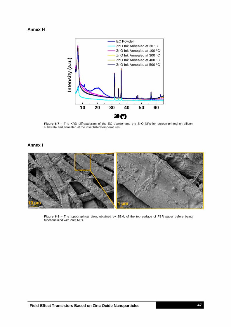
Field-Effect Transistors Based on Zinc Oxide Nanoparticles 47
Annex H
Figure 6.7 – The XRD diffractogram of the EC powder and the ZnO NPs ink screen-printed on silicon substrate and annealed at the inset listed temperatures.
Annex I
Figure 6.8 – The topographical view, obtained by SEM, of the top surface of FSR paper before being functionalized with ZnO NPs.
10 20 30 40 50 60
EC Powder
ZnO Ink Annealed at 30 C
ZnO Ink Annealed at 100 C
ZnO Ink Annealed at 300 C
ZnO Ink Annealed at 400 C
ZnO Ink Annealed at 500 C
2
Inte
ns
ity
(a
.u.)

Field-Effect Transistors Based on Zinc Oxide Nanoparticles 48
Annex J
Figure 6.9 – Total impedance |Z| variation with different frequencies.
Annex K
Table 6.1 – Extracted parameters for the selected ECM with associated error to the determination of CDL of
the lithium-based polymer electrolyte.
ECM Value Error
Rext (Ω) 117.2 8.542
Y0 (Ssα) 2.15 x 10⁻⁵ 1.91x10⁻⁷
α 0.738 0.00251
Rb (Ω) 513.3 8.317
Cb (F) 6.08 x 10⁻¹⁰ 2.36 x 10⁻¹¹
Annex L
Figure 6.10 – Schematic representation of the charge mechanism in an electrolytic parallel plate capacitor and the voltage profile plus the electric field distribuiton a) where no voltage is applied, b) instantly after the
voltage being applied, the dipolar relaxation, c) the ionic relaxation of the ions leading to the EDL starting to build up, and d) the EDL formation at the electrode/electrolyte/electrode interfaces. Adapted from [39].
10-1
100
101
102
103
104
105
106
102
103
104
105
|Z|
()
f (Hz)
ECM Fit
Data

Field-Effect Transistors Based on Zinc Oxide Nanoparticles 49
Annex M
Table 6.2 – Extracted parameters for the selected ECM with associated error to the determination of CDL of the Felix Schoeller raw paper.
ECM Value Error
Rext (Ω) 949.4 45.08
Y0 (Ssα) 1.10 x 10⁻⁶ 7.671x10⁻⁹
α 0.34 0.00274
Rb (Ω) 1.48 x 10⁵ 1.85 x 10³
Cb (F) 8.94 x 10⁻¹¹ 6.46 x 10⁻¹³
Annex N
10-2
10-1
100
10-8
10-7
10-6
10-5
Ce
ff (
Fc
m-2)
f (Hz)
-40
-30
-20
-10
0
Figure 6.11 – Magnification of the measured effective capacitance and phase (circles) and the ECM fited curves (lines) for FSR paper
Annex O
Figure 6.12 – a) Screen-printed ZnO NPs ink deposited on ITO interdigital S/D electrodes. The white lines
beneath the ZnO NPs film correspond to the patterned electrodes and b) shows an amplification of the patterned electrodes. The table in c) shows the selected number of samples for the determination of the channel length (L) for the L 200 ITO S/D interdigital electrodes.

Field-Effect Transistors Based on Zinc Oxide Nanoparticles 50
Table 6.3 – The selected number of samples for channel width (W) determination.
Number of samples for W (µm)
5082.70 5695.18 5987.67 5691.18
4966.21 5643.12 5627.03 5846.96
5034.45 5918.02 5595 6124.07
5627.10 5907.43 5677.37 6031.77
5687.14 5623.04 5647.29 6080.02
Average
5674.64
Standard Deviation
317.27
Note that W was determined at 68095.72 µm which result from multiplying the average value
by 12, which is the total number of fingers of the patterned interdigital structure (ITO or carbon), where
channel formation can take place.
Annex P
Figure 6.13 - a) Screen-printed ZnO NPs ink deposited on carbon interdigital S/D electrodes. The light grey lines correspond to the pattern electrodes and b) shows an amplification of the patterned carbon electrodes.
The table in c) depicts the selected number of samples for the determination of the channel length for the L 200 carbon S/D interdigital electrodes.
Annex Q
Table 6.4 – The determined rise and fall time (𝜏𝑟 and 𝜏𝑓, respectively) by exponential fitting on the time
response of the screen-printed ZnO NPs ink (after annealing at 300 °C) as an UV-photodetector under OFF and ON UV light radiation for 3 cycles.
Designation Time (s) Standard error
𝝉𝒓𝟏 33.99 0.21
𝝉𝒇𝟏 13.30 0.05
𝝉𝒓𝟐 20.70 0.09
𝝉𝒇𝟐 14.64 0.06
𝝉𝒓𝟑 24.74 0.14
𝝉𝒇𝟑 15.07 0.06

Field-Effect Transistors Based on Zinc Oxide Nanoparticles 51
Figure 6.14 – The time response of the screen-printed ZnO NPs ink, after annealing at 300 °C, as UV photodetector under OFF and ON UV light radiation. The blue lines correspond to the rise time (𝜏𝑟) exponential fitting while the black ones are linked to the fall time (𝜏𝑓) exponential fitting for 3 cycles.
0 200 400 600 800
0.0
0.2
0.4
0.6
0.8
1.0 Data plot
f3
f2
f1
r3
r2
Time (s)
Cu
rren
t (
A)
r1
y = y0+Ae
-x/