
Fiber Channel/Gigabit Ethernet Laser Diode Control for ... · PDF fileFN8206 Rev 2.00 Page 1...
29
FN8206 Rev 2.00 Page 1 of 29 August 20, 2007 FN8206 Rev 2.00 August 20, 2007 X9520 Fiber Channel/Gigabit Ethernet Laser Diode Control for Fiber Optic Modules Triple DCP, POR, 2kbit EEPROM Memory, Dual Voltage Monitors DATASHEET The X9520 combines three Digitally Controlled Potentiometers (DCPs), V1/VCC Power-on Reset (POR) circuitry, two programmable voltage monitor inputs with software and hardware indicators, and integrated EEPROM with Block Lock™ protection. All functions of the X9520 are accessed by an industry standard 2-Wire serial interface. Two of the DCPs of the X9520 may be utilized to control the bias and modulation currents of the laser diode in a Fiber Optic module. The third DCP may be used to set other various reference quantities, or as a coarse trim for one of the other two DCPs. The 2kbit integrated EEPROM may be used to store module definition data. The programmable POR circuit may be used to ensure that V1/VCC is stable before power is applied to the laser diode/module. The programmable voltage monitors may be used for monitoring various module alarm levels. The features of the X9520 are ideally suited to simplifying the design of fiber optic modules which comply to the Gigabit Interface Converter (GBIC) specification. The integration of these functions into one package significantly reduces board area, cost and increases reliability of laser diode modules. Features • Three Digitally Controlled Potentiometers (DCPs) - 64 Tap - 10k - 100 Tap - 10k - 256 Tap - 100k - Nonvolatile - Write Protect Function • 2kbit EEPROM Memory with Write Protect & Block Lock • 2-Wire Industry Standard Serial Interface - Complies to the Gigabit Interface Converter (GBIC) specification • Power-on Reset (POR) Circuitry - Programmable Threshold Voltage - Software Selectable Reset Timeout - Manual Reset • Two Supplementary Voltage Monitors - Programmable Threshold Voltages • Single Supply Operation - 2.7V to 5.5V • Hot Pluggable • 20 Ld Package - TSSOP • Pb-free available (RoHS compliant) Ordering Information PART NUMBER PART MARKING PRESET (FACTORY SHIPPED) TRIPx THRESHOLD LEVELS (x = 2, 3) TEMP. RANGE (°C) PACKAGE PKG. DWG. # X9520V20I-A X9520V IA Optimized for 3.3V system monitoring** -40 to +85 20 Ld TSSOP MDP0044 X9520V20I-AT1* X9520V IA Optimized for 3.3V system monitoring** -40 to +85 20 Ld TSSOP MDP0044 X9520V20I-AT2* X9520V IA Optimized for 3.3V system monitoring** -40 to +85 20 Ld TSSOP MDP0044 X9520V20I-B X9520V IB Optimized for 5V system monitoring** -40 to +85 20 Ld TSSOP MDP0044 X9520V20I-BT1* X9520V IB Optimized for 5V system monitoring** -40 to +85 20 Ld TSSOP MDP0044 X9520V20IZ-A (Note) X9520V ZIA Optimized for 3.3V system monitoring** -40 to +85 20 Ld TSSOP (Pb-free) MDP0044 X9520V20IZ-AT1* (Note) X9520V ZIA Optimized for 3.3V system monitoring** -40 to +85 20 Ld TSSOP (Pb-free) MDP0044 X9520V20IZ-AT2* (Note) X9520V ZIA Optimized for 3.3V system monitoring** -40 to +85 20 Ld TSSOP (Pb-free) MDP0044 X9520V20IZ-B (Note) X9520V ZIB Optimized for 5V system monitoring** -40 to +85 20 Ld TSSOP (Pb-free) MDP0044 X9520V20IZ-BT1* (Note) X9520V ZIB Optimized for 5V system monitoring** -40 to +85 20 Ld TSSOP (Pb-free) MDP0044 * Please refer to TB347 for details on reel specifications. ** For details, see DC Operating characteristics NOTE: These Intersil Pb-free plastic packaged products employ special Pb-free material sets; molding compounds/die attach materials and 100% matte tin plate PLUS ANNEAL - e3 termination finish, which is RoHS compliant and compatible with both SnPb and Pb-free soldering operations. Intersil Pb-free products are MSL classified at Pb-free peak reflow temperatures that meet or exceed the Pb-free requirements of IPC/JEDEC J STD-020. NOT RECOMMENDED FOR NEW DESIGNS POSSIBLE SUBSTITUTE PRODUCT ISL22343, ISL22346
Transcript of Fiber Channel/Gigabit Ethernet Laser Diode Control for ... · PDF fileFN8206 Rev 2.00 Page 1...

FN8206 Rev 2.00 Page 1 of 29August 20, 2007
FN8206Rev 2.00
August 20, 2007
X9520 Fiber Channel/Gigabit Ethernet Laser Diode Control for Fiber Optic Modules Triple DCP, POR, 2kbit EEPROM Memory, Dual Voltage Monitors
DATASHEET
The X9520 combines three Digitally Controlled Potentiometers (DCPs), V1/VCC Power-on Reset (POR) circuitry, two programmable voltage monitor inputs with software and hardware indicators, and integrated EEPROM with Block Lock™ protection. All functions of the X9520 are accessed by an industry standard 2-Wire serial interface.
Two of the DCPs of the X9520 may be utilized to control the bias and modulation currents of the laser diode in a Fiber Optic module. The third DCP may be used to set other various reference quantities, or as a coarse trim for one of the other two DCPs. The 2kbit integrated EEPROM may be used to store module definition data. The programmable POR circuit may be used to ensure that V1/VCC is stable before power is applied to the laser diode/module. The programmable voltage monitors may be used for monitoring various module alarm levels.
The features of the X9520 are ideally suited to simplifying the design of fiber optic modules which comply to the Gigabit Interface Converter (GBIC) specification. The integration of these functions into one package significantly reduces board area, cost and increases reliability of laser diode modules.
Features• Three Digitally Controlled Potentiometers (DCPs)
- 64 Tap - 10k- 100 Tap - 10k- 256 Tap - 100k- Nonvolatile
- Write Protect Function
• 2kbit EEPROM Memory with Write Protect & Block Lock
• 2-Wire Industry Standard Serial Interface
- Complies to the Gigabit Interface Converter (GBIC) specification
• Power-on Reset (POR) Circuitry
- Programmable Threshold Voltage
- Software Selectable Reset Timeout
- Manual Reset
• Two Supplementary Voltage Monitors
- Programmable Threshold Voltages
• Single Supply Operation
- 2.7V to 5.5V
• Hot Pluggable
• 20 Ld Package
- TSSOP
• Pb-free available (RoHS compliant)
Ordering Information
PART NUMBERPART
MARKINGPRESET (FACTORY SHIPPED) TRIPx
THRESHOLD LEVELS (x = 2, 3)TEMP. RANGE
(°C) PACKAGEPKG.
DWG. #
X9520V20I-A X9520V IA Optimized for 3.3V system monitoring** -40 to +85 20 Ld TSSOP MDP0044
X9520V20I-AT1* X9520V IA Optimized for 3.3V system monitoring** -40 to +85 20 Ld TSSOP MDP0044
X9520V20I-AT2* X9520V IA Optimized for 3.3V system monitoring** -40 to +85 20 Ld TSSOP MDP0044
X9520V20I-B X9520V IB Optimized for 5V system monitoring** -40 to +85 20 Ld TSSOP MDP0044
X9520V20I-BT1* X9520V IB Optimized for 5V system monitoring** -40 to +85 20 Ld TSSOP MDP0044
X9520V20IZ-A (Note) X9520V ZIA Optimized for 3.3V system monitoring** -40 to +85 20 Ld TSSOP (Pb-free) MDP0044
X9520V20IZ-AT1* (Note) X9520V ZIA Optimized for 3.3V system monitoring** -40 to +85 20 Ld TSSOP (Pb-free) MDP0044
X9520V20IZ-AT2* (Note) X9520V ZIA Optimized for 3.3V system monitoring** -40 to +85 20 Ld TSSOP (Pb-free) MDP0044
X9520V20IZ-B (Note) X9520V ZIB Optimized for 5V system monitoring** -40 to +85 20 Ld TSSOP (Pb-free) MDP0044
X9520V20IZ-BT1* (Note) X9520V ZIB Optimized for 5V system monitoring** -40 to +85 20 Ld TSSOP (Pb-free) MDP0044
* Please refer to TB347 for details on reel specifications.** For details, see DC Operating characteristicsNOTE: These Intersil Pb-free plastic packaged products employ special Pb-free material sets; molding compounds/die attach materials and 100% matte tin plate PLUS ANNEAL - e3 termination finish, which is RoHS compliant and compatible with both SnPb and Pb-free soldering operations. Intersil Pb-free products are MSL classified at Pb-free peak reflow temperatures that meet or exceed the Pb-free requirements of IPC/JEDEC J STD-020.
NOT RECOMMENDED FOR NEW DESIGNSPOSSIBLE SUBSTITUTE PRODUCT
ISL22343, ISL22346

X9520
Block Diagram
Detailed Device DescriptionThe X9520 combines three Intersil Digitally Controlled Potentiometer (DCP) devices, V1/VCC power-on reset control, V1/VCC low voltage reset control, two supplementary voltage monitors, and integrated EEPROM with Block Lock™ protection, in one package. These functions are suited to the control, support, and monitoring of various system parameters in Fiber Channel/Gigabit Ethernet fiber optic modules, such as in Gigabit Interface Converter (GBIC) applications. The combination of the X9520 fucntionality lowers system cost, increases reliability, and reduces board space requirements using Intersil’s unique XBGA™ packaging.
Two high resolution DCPs allow for the “set-and-forget” adjustment of Laser Driver IC parameters such as Laser Diode Bias and Modulation Currents. One lower resolution DCP may be used for setting sundry system parameters such as maximum laser output power (for eye safety requirements).
Applying voltage to VCC activates the Power-on Reset circuit which allows the V1RO output to go HIGH, until the supply the supply voltage stabilizes for a period of time (selectable via software). The V1RO output then goes LOW. The Low Voltage Reset circuitry allows the V1RO output to go HIGH when VCC falls below the minimum VCC trip point. V1RO remains HIGH until VCC returns to proper operating level. A Manual Reset (MR) input allows the user to externally trigger the V1RO output (HIGH).
Two supplementary Voltage Monitor circuits continuously compare their inputs to individual trip voltages. If an input voltage exceeds it’s associated trip level, a hardware output (V3RO, V2RO) are allowed to go HIGH. If the input voltage becomes lower than it’s associated trip level, the corresponding output is driven LOW. A corresponding binary representation of the two monitor circuit outputs (V2RO and V3RO) are also stored in latched, volatile (CONSTAT) register bits. The status of these two monitor outputs can be read out via the 2-wire serial port.
An application of the V1RO output may be to drive the “ENABLE” input of a Laser Driver IC, with MR as a “TX_DISABLE” input. V2RO and V3RO may be used to monitor “TX_FAULT” and “RX_LOS” conditions respectively.
Intersil’s unique circuits allow for all internal trip voltages to be individually programmed with high accuracy. This gives the designer great flexibility in changing system parameters, either at the time of manufacture, or in the field.
The memory portion of the device is a CMOS serial EEPROM array with Intersil’s Block Lock™ protection. This memory may be used to store fiber optic module manufacturing data, serial numbers, or various other system parameters. The EEPROM array is internally organized as x 8, and utilizes Intersil’s proprietary Direct Write™ cells, providing a minimum endurance of 1,000,000 cycles and a minimum data retention of 100 years.
The device features a 2-Wire interface and software protocol allowing operation on an I2C™ compatible serial bus.
DATAREGISTER
COMMAND
DECODE &
CONTROL
LOGIC
SDA
SCL
POWER-ON /LOW VOLTAGE
CONSTATREGISTER
PROTECT LOGIC
EEPROM
THRESHOLD
RESET LOGIC
4
GENERATIONRESET
V2VTRIP
V1/VCC
VTRIP
V3+-
2
3
1
2kbit
V1RO
RH2
RW2
RL2MR
86 - BIT
NONVOLATILEMEMORY
RH0
RW0
RL0
WIPER
REGISTER
RH1
RW1
RL1
COUNTER
V2RO
WP
V3RO
7 - BITNONVOLATILE
MEMORY
NONVOLATILEMEMORY
WIPER
REGISTERCOUNTER
WIPER
REGISTERCOUNTER
ARRAY
8 - BIT2
VTRIP
+-
+-
FN8206 Rev 2.00 Page 2 of 29August 20, 2007

X9520
PinoutX9520
(20 LD TSSOP)TOP VIEW
V2
RL2
RH0
3
4
V1/VCC
SCL
RW0
RL0
RW1
RH1
7
8
V3
VSS 10 RL1
RH2 1
18
19
17
20
14
15
13
16
12
11
MR 6
RW2 2
SDA 9
V3RO 5
WP
V1RO
V2RO
NOT TO SCALE
Pin Descriptions
TSSOP NAME FUNCTION
1 RH2 Connection to end of resistor array for (the 256 Tap) DCP 2.
2 Rw2 Connection to terminal equivalent to the “Wiper” of a mechanical potentiometer for DCP 2.
3 RL2 Connection to other end of resistor array for (the 256 Tap) DCP 2.
4 V3 V3 Voltage Monitor Input. V3 is the input to a non-inverting voltage comparator circuit. When the V3 input is higher than the VTRIP3 threshold voltage, V3RO makes a transition to a HIGH level. Connect V3 to VSS when not used.
5 V3RO V3 RESET Output. This open drain output makes a transition to a HIGH level when V3 is greater than VTRIP3 and goes LOW when V3 is less than VTRIP3. There is no delay circuitry on this pin. The V3RO pin requires the use of an external “pull-up” resistor.
6 MR Manual Reset. MR is a TTL level compatible input. Pulling the MR pin active (HIGH) initiates a reset cycle to the V1RO pin (V1/VCC RESET Output pin). V1RO will remain HIGH for time tpurst after MR has returned to it’s normally LOW state. The reset time can be selected using bits POR1 and POR0 in the CONSTAT Register. The MR pin requires the use of an external “pull-down” resistor.
7 WP Write Protect Control Pin. WP pin is a TTL level compatible input. When held HIGH, Write Protection is enabled. In the enabled state, this pin prevents all nonvolatile “write” operations. Also, when the Write Protection is enabled, and the device Block Lock feature is active (i.e. the Block Lock bits are NOT [0,0]), then no “write” (volatile or nonvolatile) operations can be performed in the device (including the wiper position of any of the integrated Digitally Controlled Potentiometers (DCPs). The WP pin uses an internal “pull-down” resistor, thus if left floating the write protection feature is disabled.
8 SCL Serial Clock. This is a TTL level compatible input pin used to control the serial bus timing for data input and output.
9 SDA Serial Data. SDA is a bidirectional TTL level compatible pin used to transfer data into and out of the device. The SDA pin input buffer is always active (not gated). This pin requires an external pull up resistor.
10 Vss Ground.
11 RL1 Connection to other end of resistor for (the 100 Tap) DCP 1.
12 Rw1 Connection to terminal equivalent to the “Wiper” of a mechanical potentiometer for DCP 1.
13 RH1 Connection to end of resistor array for (the 100 Tap) DCP 1.
14 RH0 Connection to end of resistor array for (the 64 Tap) Digitally Controlled Potentiometer (DCP) 0.
15 RW0 Connection to terminal equivalent to the “Wiper” of a mechanical potentiometer for DCP 0.
16 RL0 Connection to the other end of resistor array for (the 64 Tap) DCP 0.
17 V2 V2 Voltage Monitor Input. V2 is the input to a non-inverting voltage comparator circuit. When the V2 input is greater than the VTRIP2 threshold voltage, V2RO makes a transition to a HIGH level. Connect V2 to VSS when not used.
18 V2RO V2 RESET Output. This open drain output makes a transition to a HIGH level when V2 is greater than VTRIP2, and goes LOW when V2 is less than VTRIP2. There is no power-up reset delay circuitry on this pin. The V2RO pin requires the use of an external “pull-up” resistor.
FN8206 Rev 2.00 Page 3 of 29August 20, 2007

X9520
Principles of Operation
Serial Interface
SERIAL INTERFACE CONVENTIONS
The device supports a bidirectional bus oriented protocol. The protocol defines any device that sends data onto the bus as a transmitter, and the receiving device as the receiver. The device controlling the transfer is called the master and the device being controlled is called the slave. The master always initiates data transfers, and provides the clock for both transmit and receive operations. Therefore, the X9520 operates as a slave in all applications.
SERIAL CLOCK AND DATA
Data states on the SDA line can change only while SCL is LOW. SDA state changes while SCL is HIGH are reserved for indicating START and STOP conditions. See Figure 1. On power-up of the X9520, the SDA pin is in the input mode.
SERIAL START CONDITION
All commands are preceded by the START condition, which is a HIGH to LOW transition of SDA while SCL is HIGH. The device continuously monitors the SDA and SCL lines for the
START condition and does not respond to any command until this condition has been met. See Figure 2.
SERIAL STOP CONDITION
All communications must be terminated by a STOP condition, which is a LOW to HIGH transition of SDA while SCL is HIGH. The STOP condition is also used to place the device into the Standby power mode after a read sequence. A STOP condition can only be issued after the transmitting device has released the bus. See Figure 2.
19 V1RO V1/VCC RESET Output. This is an active HIGH, open drain output which becomes active whenever V1/VCC falls below VTRIP1. V1RO becomes active on power-up and remains active for a time tpurst after the power supply stabilizes (tpurst can be changed by varying the POR0 and POR1 bits of the internal control register). The V1RO pin requires the use of an external “pull-up” resistor. The V1RO pin can be forced active (HIGH) using the manual reset (MR) input pin.
20 V1/VCC Supply Voltage.
Pin Descriptions (Continued)
TSSOP NAME FUNCTION
SCL
SDA
DATA STABLE DATA CHANGE DATA STABLE
FIGURE 1. VALID DATA CHANGES ON THE SDA BUS
SCL
SDA
START STOP
FIGURE 2. VALID START AND STOP CONDITIONS
FN8206 Rev 2.00 Page 4 of 29August 20, 2007

X9520
SERIAL ACKNOWLEDGE
An ACKNOWLEDGE (ACK) is a software convention used to indicate a successful data transfer. The transmitting device, either master or slave, will release the bus after transmitting eight bits. During the ninth clock cycle, the receiver will pull the SDA line LOW to ACKNOWLEDGE that it received the eight bits of data. Refer to Figure 3.
The device will respond with an ACKNOWLEDGE after recognition of a START condition if the correct Device Identifier bits are contained in the Slave Address Byte. If a write operation is selected, the device will respond with an ACKNOWLEDGE after the receipt of each subsequent eight bit word.
In the read mode, the device will transmit eight bits of data, release the SDA line, then monitor the line for an ACKNOWLEDGE. If an ACKNOWLEDGE is detected and no STOP condition is generated by the master, the device will continue to transmit data. The device will terminate further data transmissions if an ACKNOWLEDGE is not detected. The master must then issue a STOP condition to place the device into a known state.
Device Internal Addressing
Addressing Protocol Overview
The user addressable internal components of the X9520 can be split up into three main parts:
• Three Digitally Controlled Potentiometers (DCPs)
• EEPROM array
• Control and Status (CONSTAT) Register
Depending upon the operation to be performed on each of these individual parts, a 1, 2 or 3 Byte protocol is used. All operations however must begin with the Slave Address Byte being issued on the SDA pin. The Slave address selects the part of the X9520 to be addressed, and specifies if a Read or Write operation is to be performed.
It should be noted that in order to perform a write operation to either a DCP or the EEPROM array, the Write Enable Latch (WEL) bit must first be set (See “BL1, BL0: Block Lock protection bits - (Nonvolatile)” on page 13.)
Slave Address Byte
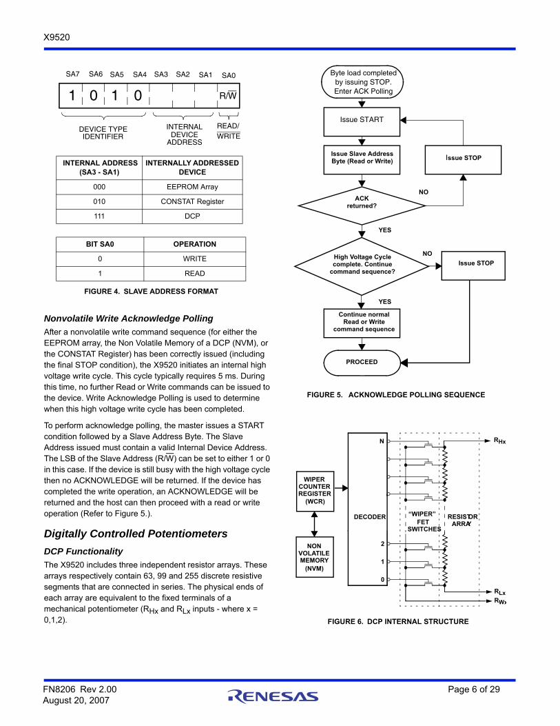
Following a START condition, the master must output a Slave Address Byte (Refer to Figure 4). This byte consists of three parts:
• The Device Type Identifier which consists of the most significant four bits of the Slave Address (SA7 - SA4). The Device Type Identifier must always be set to 1010 in order to select the X9520.
• The next three bits (SA3 - SA1) are the Internal Device Address bits. Setting these bits to 000 internally selects the EEPROM array, while setting these bits to 111 selects the DCP structures in the X9520. The CONSTAT Register may be selected using the Internal Device Address 010.
• The Least Significant Bit of the Slave Address (SA0) Byte is the R/W bit. This bit defines the operation to be performed on the device being addressed (as defined in the bits SA3 - SA1). When the R/W bit is “1”, then a READ operation is selected. A “0” selects a WRITE operation (Refer to Figure 4.)
SCL from
MasterData Output from
Transmitter
Data Output from Receiver
81 9
START ACKNOWLEDGE
FIGURE 3. ACKNOWLEDGE RESPONSE FROM RECEIVER
SCL from Master
FN8206 Rev 2.00 Page 5 of 29August 20, 2007
X9520
Nonvolatile Write Acknowledge Polling
After a nonvolatile write command sequence (for either the EEPROM array, the Non Volatile Memory of a DCP (NVM), or the CONSTAT Register) has been correctly issued (including the final STOP condition), the X9520 initiates an internal high voltage write cycle. This cycle typically requires 5 ms. During this time, no further Read or Write commands can be issued to the device. Write Acknowledge Polling is used to determine when this high voltage write cycle has been completed.
To perform acknowledge polling, the master issues a START condition followed by a Slave Address Byte. The Slave Address issued must contain a valid Internal Device Address. The LSB of the Slave Address (R/W) can be set to either 1 or 0 in this case. If the device is still busy with the high voltage cycle then no ACKNOWLEDGE will be returned. If the device has completed the write operation, an ACKNOWLEDGE will be returned and the host can then proceed with a read or write operation (Refer to Figure 5.).
Digitally Controlled Potentiometers
DCP Functionality
The X9520 includes three independent resistor arrays. These arrays respectively contain 63, 99 and 255 discrete resistive segments that are connected in series. The physical ends of each array are equivalent to the fixed terminals of a mechanical potentiometer (RHx and RLx inputs - where x = 0,1,2).
SA6SA7 SA5 SA3 SA2 SA1 SA0
DEVICE TYPEIDENTIFIER
READ/
SA4
INTERNAL ADDRESS (SA3 - SA1)
INTERNALLY ADDRESSED DEVICE
000 EEPROM Array
010 CONSTAT Register
111 DCP
BIT SA0 OPERATION
0 WRITE
1 READ
R/W
FIGURE 4. SLAVE ADDRESS FORMAT
1 0 1 0
WRITEADDRESS
INTERNALDEVICE
ACK returned?
Issue Slave Address Byte (Read or Write)
Byte load completed by issuing STOP.Enter ACK Polling
Issue STOP
Issue START
NO
YES
High Voltage Cycle complete. Continue
command sequence?Issue STOP
NO
Continue normal Read or Write
command sequence
PROCEED
YES
FIGURE 5. ACKNOWLEDGE POLLING SEQUENCE
DECODER RESISTORARRAY
RHx
FETSWITCHES
RLxRWx
0
1
2
N
WIPER
REGISTERCOUNTER
NON
MEMORYVOLATILE
(WCR)
(NVM)
“WIPER”
FIGURE 6. DCP INTERNAL STRUCTURE
FN8206 Rev 2.00 Page 6 of 29August 20, 2007
X9520
At both ends of each array and between each resistor segment there is a CMOS switch connected to the wiper (Rwx) output. Within each individual array, only one switch may be turned on at any one time. These switches are controlled by the Wiper Counter Register (WCR) (See Figure 6). The WCR is a volatile register.
On power-up of the X9520, wiper position data is automatically loaded into the WCR from its associated Non Volatile Memory (NVM) Register. The table below shows the Initial Values of the DCP WCR’s before the contents of the NVM is loaded into the WCR.
The data in the WCR is then decoded to select and enable one of the respective FET switches. A “make before break” sequence is used internally for the FET switches when the wiper is moved from one tap position to another.
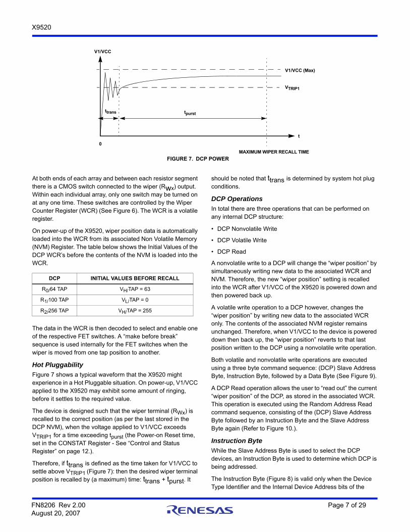
Hot Pluggability
Figure 7 shows a typical waveform that the X9520 might experience in a Hot Pluggable situation. On power-up, V1/VCC applied to the X9520 may exhibit some amount of ringing, before it settles to the required value.
The device is designed such that the wiper terminal (RWx) is recalled to the correct position (as per the last stored in the DCP NVM), when the voltage applied to V1/VCC exceeds VTRIP1 for a time exceeding tpurst (the Power-on Reset time, set in the CONSTAT Register - See “Control and Status Register” on page 12.).
Therefore, if ttrans is defined as the time taken for V1/VCC to settle above VTRIP1 (Figure 7): then the desired wiper terminal position is recalled by (a maximum) time: ttrans + tpurst. It
should be noted that ttrans is determined by system hot plug conditions.
DCP Operations
In total there are three operations that can be performed on any internal DCP structure:
• DCP Nonvolatile Write
• DCP Volatile Write
• DCP Read
A nonvolatile write to a DCP will change the “wiper position” by simultaneously writing new data to the associated WCR and NVM. Therefore, the new “wiper position” setting is recalled into the WCR after V1/VCC of the X9520 is powered down and then powered back up.
A volatile write operation to a DCP however, changes the “wiper position” by writing new data to the associated WCR only. The contents of the associated NVM register remains unchanged. Therefore, when V1/VCC to the device is powered down then back up, the “wiper position” reverts to that last position written to the DCP using a nonvolatile write operation.
Both volatile and nonvolatile write operations are executed using a three byte command sequence: (DCP) Slave Address Byte, Instruction Byte, followed by a Data Byte (See Figure 9).
A DCP Read operation allows the user to “read out” the current “wiper position” of the DCP, as stored in the associated WCR. This operation is executed using the Random Address Read command sequence, consisting of the (DCP) Slave Address Byte followed by an Instruction Byte and the Slave Address Byte again (Refer to Figure 10.).
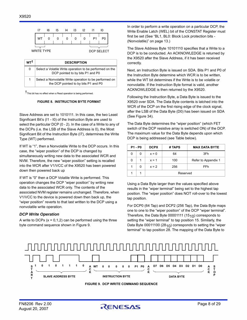
Instruction Byte
While the Slave Address Byte is used to select the DCP devices, an Instruction Byte is used to determine which DCP is being addressed.
The Instruction Byte (Figure 8) is valid only when the Device Type Identifier and the Internal Device Address bits of the
DCP INITIAL VALUES BEFORE RECALL
R0/64 TAP VH/TAP = 63
R1/100 TAP VL/TAP = 0
R2/256 TAP VH/TAP = 255
FIGURE 7. DCP POWER
t
V1/VCC
VTRIP1
V1/VCC (Max)
tpurst
MAXIMUM WIPER RECALL TIME
0
ttrans
FN8206 Rev 2.00 Page 7 of 29August 20, 2007
X9520
Slave Address are set to 1010111. In this case, the two Least Significant Bit’s (I1 - I0) of the Instruction Byte are used to select the particular DCP (0 - 2). In the case of a Write to any of the DCPs (i.e. the LSB of the Slave Address is 0), the Most Significant Bit of the Instruction Byte (I7), determines the Write Type (WT) performed.
If WT is “1”, then a Nonvolatile Write to the DCP occurs. In this case, the “wiper position” of the DCP is changed by simultaneously writing new data to the associated WCR and NVM. Therefore, the new “wiper position” setting is recalled into the WCR after V1/VCC of the X9520 has been powered down then powered back up
If WT is “0” then a DCP Volatile Write is performed. This operation changes the DCP “wiper position” by writing new data to the associated WCR only. The contents of the associated NVM register remains unchanged. Therefore, when V1/VCC to the device is powered down then back up, the “wiper position” reverts to that last written to the DCP using a nonvolatile write operation.
DCP Write Operation
A write to DCPx (x = 0,1,2) can be performed using the three byte command sequence shown in Figure 9.
In order to perform a write operation on a particular DCP, the Write Enable Latch (WEL) bit of the CONSTAT Register must first be set (See “BL1, BL0: Block Lock protection bits - (Nonvolatile)” on page 13.)
The Slave Address Byte 10101110 specifies that a Write to a DCP is to be conducted. An ACKNOWLEDGE is returned by the X9520 after the Slave Address, if it has been received correctly.
Next, an Instruction Byte is issued on SDA. Bits P1 and P0 of the Instruction Byte determine which WCR is to be written, while the WT bit determines if the Write is to be volatile or nonvolatile. If the Instruction Byte format is valid, another ACKNOWLEDGE is then returned by the X9520.
Following the Instruction Byte, a Data Byte is issued to the X9520 over SDA. The Data Byte contents is latched into the WCR of the DCP on the first rising edge of the clock signal, after the LSB of the Data Byte (D0) has been issued on SDA (See Figure 34).
The Data Byte determines the “wiper position” (which FET switch of the DCP resistive array is switched ON) of the DCP. The maximum value for the Data Byte depends upon which DCP is being addressed (see Table below).
Using a Data Byte larger than the values specified above results in the “wiper terminal” being set to the highest tap position. The “wiper position” does NOT roll-over to the lowest tap position.
For DCP0 (64 Tap) and DCP2 (256 Tap), the Data Byte maps one to one to the “wiper position” of the DCP “wiper terminal”. Therefore, the Data Byte 00001111 (1510) corresponds to setting the “wiper terminal” to tap position 15. Similarly, the Data Byte 00011100 (2810) corresponds to setting the “wiper terminal” to tap position 28. The mapping of the Data Byte to
WT† DESCRIPTION
0 Select a Volatile Write operation to be performed on the DCP pointed to by bits P1 and P0
1 Select a Nonvolatile Write operation to be performed on the DCP pointed to by bits P1 and P0
00WT 0 0 0 P1 P0
WRITE TYPE DCP SELECT
†This bit has no effect when a Read operation is being performed.
I5I6I7 I4 I3 I2 I1 I0
FIGURE 8. INSTRUCTION BYTE FORMAT
P1 - P0 DCPX # TAPS MAX DATA BYTE
0 0 x = 0 64 3Fh
0 1 x = 1 100 Refer to Appendix 1
1 0 x = 2 256 FFh
1 1 Reserved
START
1 0 1 0 1 1 1 0 ACK
WT 0 0 0 0 0 P1 P0 ACK
STOP
ACK
D7 D6 D5 D4 D3 D2 D1 D0
SLAVE ADDRESS BYTE INSTRUCTION BYTE DATA BYTE
FIGURE 9. DCP WRITE COMMAND SEQUENCE
FN8206 Rev 2.00 Page 8 of 29August 20, 2007

X9520
“wiper position” data for DCP1 (100 Tap), is shown in “Appendix 1” . An example of a simple C language function which “translates” between the tap position (decimal) and the Data Byte (binary) for DCP1, is given in “Appendix 2” .
It should be noted that all writes to any DCP of the X9520 are random in nature. Therefore, the Data Byte of consecutive write operations to any DCP can differ by an arbitrary number of bits. Also, setting the bits P1 = 1, P0 = 1 is a reserved sequence, and will result in no ACKNOWLEDGE after sending an Instruction Byte on SDA.
The factory default setting of all “wiper position” settings is with 00h stored in the NVM of the DCPs. This corresponds to having the “wiper teminal” RWX (x = 0,1,2) at the “lowest” tap position, Therefore, the resistance between RWX and RLX is a minimum (essentially only the Wiper Resistance, RW).
DCP Read Operation
A read of DCPx (x = 0,1,2) can be performed using the three byte random read command sequence shown in Figure 10.
The master issues the START condition and the Slave Address Byte 10101110 which specifies that a “dummy” write” is to be
conducted. This “dummy” write operation sets which DCP is to be read (in the preceding Read operation). An ACKNOWLEDGE is returned by the X9520 after the Slave Address if received correctly. Next, an Instruction Byte is issued on SDA. Bits P1-P0 of the Instruction Byte determine which DCP “wiper position” is to be read. In this case, the state of the WT bit is “don’t care”. If the Instruction Byte format is valid, then another ACKNOWLEDGE is returned by the X9520.
Following this ACKNOWLEDGE, the master immediately issues another START condition and a valid Slave address byte with the R/W bit set to 1. Then the X9520 issues an ACKNOWLEDGE followed by Data Byte, and finally, the master issues a STOP condition. The Data Byte read in this operation, corresponds to the “wiper position” (value of the WCR) of the DCP pointed to by bits P1 and P0.
It should be noted that when reading out the data byte for DCP0 (64 Tap), the upper two most significant bits are “unknown” bits. For DCP1 (100 Tap), the upper most significant bit is an “unknown”. For DCP2 (256 Tap) however, all bits of the data byte are relevant (See Figure 10).
Slave Address
InstructionByte
ACK
ACK
Start
Stop
Slave Address
Data Byte
ACK
Start
SDA Bus
Signals from the Slave
Signals from the Master
FIGURE 10. DCP READ SEQUENCE
“Dummy” write
READ Operation
1 0 1 1 1 1 00 0 0 0 00WT
P1
P0 1 0 1 1 1 1 10
WRITE Operation
-
- -
MSB LSB
DCPx
x = 0
x = 1
x = 2
“-” = DON’T CARE
Start
Stop
Slave Address
AddressByte
DataByte
ACK
ACK
ACK
SDA Bus
Signals from the Slave
Signals from the Master
FIGURE 11. EEPROM BYTE WRITE SEQUENCE
Internal Device
Address
1 0 1 0 0 0 0 0
WRITE Operation
FN8206 Rev 2.00 Page 9 of 29August 20, 2007

X9520
2KBIT EEPROM ARRAY
Operations on the 2kbit EEPROM Array, consist of either 1, 2 or 3 byte command sequences. All operations on the EEPROM must begin with the Device Type Identifier of the Slave Address set to 1010000. A Read or Write to the EEPROM is selected by setting the LSB of the Slave Address to the appropriate value R/W (Read = “1”, Write = ”0”).
In some cases when performing a Read or Write to the EEPROM, an Address Byte may also need to be specified. This Address Byte can contain the values 00h to FFh.
EEPROM BYTE WRITE
In order to perform an EEPROM Byte Write operation to the EEPROM array, the Write Enable Latch (WEL) bit of the CONSTAT Register must first be set (See “BL1, BL0: Block Lock protection bits - (Nonvolatile)” on page 13.)
For a write operation, the X9520 requires the Slave Address Byte and an Address Byte. This gives the master access to any one of the words in the array. After receipt of the Address Byte, the X9520 responds with an ACKNOWLEDGE, and awaits the next eight bits of data. After receiving the 8 bits of the Data Byte, it again responds with an ACKNOWLEDGE. The master then terminates the transfer by generating a STOP condition, at which time the X9520 begins the internal write cycle to the nonvolatile memory (See Figure 11). During this internal write cycle, the X9520 inputs are disabled, so it does not respond to any requests from the master. The SDA output is at high impedance. A write to a region of EEPROM memory which has been protected with the Block-Lock feature (See “BL1, BL0: Block Lock protection bits - (Nonvolatile)” on page 13.), suppresses the ACKNOWLEDGE bit after the Address Byte.
EEPROM Page Write
In order to perform an EEPROM Page Write operation to the EEPROM array, the Write Enable Latch (WEL) bit of the CONSTAT Register must first be set (See “BL1, BL0: Block Lock protection bits - (Nonvolatile)” on page 13.)
The X9520 is capable of a page write operation. It is initiated in the same manner as the byte write operation; but instead of
terminating the write cycle after the first data byte is transferred, the master can transmit an unlimited number of 8-bit bytes. After the receipt of each byte, the X9520 responds with an ACKNOWLEDGE, and the address is internally incremented by one. The page address remains constant. When the counter reaches the end of the page, it “rolls over” and goes back to ‘0’ on the same page.
For example, if the master writes 12 bytes to the page starting at location 11 (decimal), the first 5 bytes are written to locations 11 through 15, while the last 7 bytes are written to locations 0 through 6. Afterwards, the address counter would point to location 7. If the master supplies more than 16 bytes of data, then new data overwrites the previous data, one byte at a time (See Figure 13).
The master terminates the Data Byte loading by issuing a STOP condition, which causes the X9520 to begin the nonvolatile write cycle. As with the byte write operation, all inputs are disabled until completion of the internal write cycle. See Figure 12 for the address, ACKNOWLEDGE, and data transfer sequence.
Stops and EEPROM Write Modes
Stop conditions that terminate write operations must be sent by the master after sending at least 1 full data byte and receiving the subsequent ACKNOWLEDGE signal. If the master issues a STOP within a Data Byte, or before the X9520 issues a corresponding ACKNOWLEDGE, the X9520 cancels the write operation. Therefore, the contents of the EEPROM array does not change.
EEPROM Array Read Operations
Read operations are initiated in the same manner as write operations with the exception that the R/W bit of the Slave Address Byte is set to one. There are three basic read operations: Current EEPROM Address Read, Random EEPROM Read, and Sequential EEPROM Read.
Current EEPROM Address Read
Internally the device contains an address counter that maintains the address of the last word read incremented by one. Therefore, if the last read was to address n, the next read
Start
Stop
Slave Address
AddressByte
Data(n)
ACK
ACK
ACK
SDA Bus
Signals from the Slave
Signals from the Master
Data(1)
ACK
(2 < n < 16)
FIGURE 12. EEPROM PAGE WRITE OPERATION
1 0 1 0 0 0 0 0
FN8206 Rev 2.00 Page 10 of 29August 20, 2007

X9520
operation would access data from address n+1. On power-up, the address of the address counter is undefined, requiring a read or write operation for initialization.
Upon receipt of the Slave Address Byte with the R/W bit set to one, the device issues an ACKNOWLEDGE and then transmits the eight bits of the Data Byte. The master terminates the read operation when it does not respond with an ACKNOWLEDGE during the ninth clock and then issues a STOP condition (See Figure 14 for the address, ACKNOWLEDGE, and data transfer sequence).
It should be noted that the ninth clock cycle of the read operation is not a “don’t care.” To terminate a read operation, the master must either issue a STOP condition during the ninth cycle or hold SDA HIGH during the ninth clock cycle and then issue a STOP condition.
Another important point to note regarding the “Current EEPROM Address Read” , is that this operation is not available if the last executed operation was an access to a DCP or the CONSTAT Register (i.e.: an operation using the Device Type Identifier 1010111 or 1010010). Immediately after an operation
ADDRESS = 1110
5 bytes7 BYTES
ADDRESS = 610
ADDRESS POINTER
ENDS HEREADDRESS = 710
FIGURE 13. EXAMPLE: WRITING 12 BYTES TO A 16-BYTE PAGE STARTING AT LOCATION 11.
5 BYTES
ADDRESS = 1510
START
STOP
SLAVE ADDRESS
DATA
ACK
SDA BUS
SIGNALS FROM THE SLAVE
SIGNALS FROM THE MASTER
1
FIGURE 14. CURRENT EEPROM ADDRESS READ SEQUENCE
1 0 00001
0
Slave Address
Address Byte
ACK
ACK
Start
Stop
Slave Address
Data
ACK
1
Start
SDA Bus
Signals from the Slave
Signals from the Master
FIGURE 15. RANDOM EEPROM ADDRESS READ SEQUENCE
WRITE Operation
“Dummy” Write
READ Operation
1 0 000011 0 00001
FN8206 Rev 2.00 Page 11 of 29August 20, 2007
X9520
to a DCP or CONSTAT Register is performed, only a “Random EEPROM Read” is available. Immediately following a “Random EEPROM Read” , a “Current EEPROM Address Read” or “Sequential EEPROM Read” is once again available (assuming that no access to a DCP or CONSTAT Register occur in the interim).
Random EEPROM Read
Random read operation allows the master to access any memory location in the array. Prior to issuing the Slave Address Byte with the R/W bit set to one, the master must first perform a “dummy” write operation. The master issues the START condition and the Slave Address Byte, receives an ACKNOWLEDGE, then issues an Address Byte. This “dummy” Write operation sets the address pointer to the address from which to begin the random EEPROM read operation.
After the X9520 acknowledges the receipt of the Address Byte, the master immediately issues another START condition and the Slave Address Byte with the R/W bit set to one. This is followed by an ACKNOWLEDGE from the X9520 and then by the eight bit word. The master terminates the read operation by not responding with an ACKNOWLEDGE and instead issuing a STOP condition (Refer to Figure 15.).
A similar operation called “Set Current Address” also exists. This operation is performed if a STOP is issued instead of the second START shown in Figure 15. In this case, the device sets the address pointer to that of the Address Byte, and then goes into standby mode after the STOP bit. All bus activity will be ignored until another START is detected.
Sequential EEPROM Read
Sequential reads can be initiated as either a current address read or random address read. The first Data Byte is transmitted as with the other modes; however, the master now responds with an ACKNOWLEDGE, indicating it requires additional data. The X9520 continues to output a Data Byte for each ACKNOWLEDGE received. The master terminates the read operation by not responding with an ACKNOWLEDGE and instead issuing a STOP condition.
The data output is sequential, with the data from address n followed by the data from address n + 1. The address counter for read operations increments through the entire memory contents to be serially read during one operation. At the end of the address space the counter “rolls over” to address 00h and the device continues to output data for each ACKNOWLEDGE received (Refer to Figure 16.).
Control and Status Register
The Control and Status (CONSTAT) Register provides the user with a mechanism for changing and reading the status of various parameters of the X9520 (See Figure 17).
The CONSTAT register is a combination of both volatile and nonvolatile bits. The nonvolatile bits of the CONSTAT register retain their stored values even when V1/VCC is powered down, then powered back up. The volatile bits however, will always power-up to a known logic state “0” (irrespective of their value at power-down).
Data(2)
Stop
Slave Address
Data(n)
ACK
ACK
SDA Bus
Signals from the Slave
Signals from the Master
1
Data(n-1)
ACK
ACK
(n is any integer greater than 1)
Data(1)
FIGURE 16. SEQUENTIAL EEPROM READ SEQUENCE
0 0 0
BIT(S) DESCRIPTION
WEL Write Enable Latch bit
RWEL Register Write Enable Latch bit
V2OS V2 Output Status flag
V3OS V3 Output Status flag
BL1 - BL0 Sets the Block Lock partition
POR1 - POR0 Sets the Power-on Reset time
POR1 WEL POR0
CS5CS6CS7 CS4 CS3 CS2 CS1 CS0
V3OSV2OS BL0BL1 RWEL
FIGURE 17. CONSTAT REGISTER FORMAT
NV NVNVNV
NOTE: Bits labelled NV are nonvolatile (See “CONTROL AND STATUS REGISTER”).
FN8206 Rev 2.00 Page 12 of 29August 20, 2007
X9520
A detailed description of the function of each of the CONSTAT register bits follows:
WEL: WRITE ENABLE LATCH (VOLATILE)
The WEL bit controls the Write Enable status of the entire X9520 device. This bit must first be enabled before ANY write operation (to DCPs, EEPROM memory array, or the CONSTAT register). If the WEL bit is not first enabled, then ANY proceeding (volatile or nonvolatile) write operation to DCPs, EEPROM array, as well as the CONSTAT register, is aborted and no ACKNOWLEDGE is issued after a Data Byte.
The WEL bit is a volatile latch that powers up in the disabled, LOW (0) state. The WEL bit is enabled/set by writing 00000010 to the CONSTAT register. Once enabled, the WEL bit remains set to “1” until either it is reset to “0” (by writing 00000000 to the CONSTAT register) or until the X9520 powers down, and then up again.
Writes to the WEL bit do not cause an internal high voltage write cycle. Therefore, the device is ready for another operation immediately after a STOP condition is executed in the CONSTAT Write command sequence (See Figure 18).
RWEL: REGISTER WRITE ENABLE LATCH (VOLATILE)
The RWEL bit controls the (CONSTAT) Register Write Enable status of the X9520. Therefore, in order to write to any of the bits of the CONSTAT Register (except WEL), the RWEL bit must first be set to “1”. The RWEL bit is a volatile bit that powers up in the disabled, LOW (“0”) state.
It must be noted that the RWEL bit can only be set, once the WEL bit has first been enabled (See "CONSTAT Register Write Operation").
The RWEL bit will reset itself to the default “0” state, in one of three cases:
• After a successful write operation to any bits of the CONSTAT register has been completed (See Figure 18).
• When the X9520 is powered down.
• When attempting to write to a Block Lock protected region of the EEPROM memory (See "BL1, BL0: Block Lock protection bits - (Nonvolatile)").
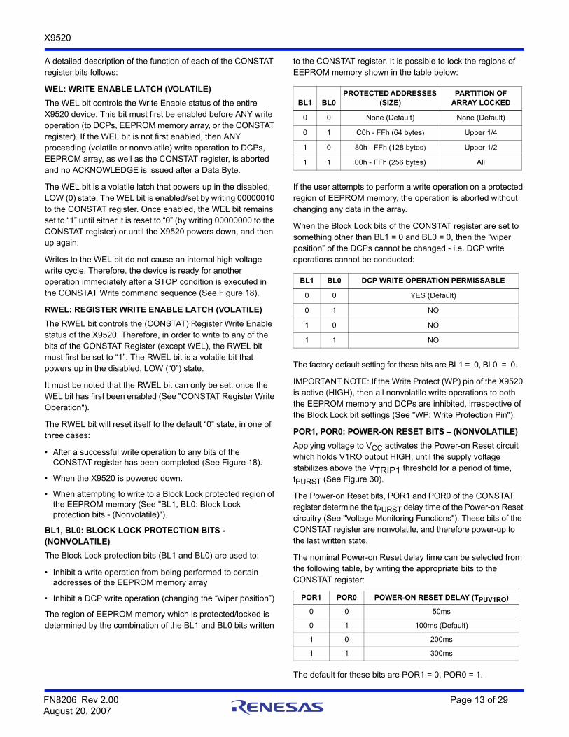
BL1, BL0: BLOCK LOCK PROTECTION BITS - (NONVOLATILE)
The Block Lock protection bits (BL1 and BL0) are used to:
• Inhibit a write operation from being performed to certain addresses of the EEPROM memory array
• Inhibit a DCP write operation (changing the “wiper position”)
The region of EEPROM memory which is protected/locked is determined by the combination of the BL1 and BL0 bits written
to the CONSTAT register. It is possible to lock the regions of EEPROM memory shown in the table below:
If the user attempts to perform a write operation on a protected region of EEPROM memory, the operation is aborted without changing any data in the array.
When the Block Lock bits of the CONSTAT register are set to something other than BL1 = 0 and BL0 = 0, then the “wiper position” of the DCPs cannot be changed - i.e. DCP write operations cannot be conducted:
The factory default setting for these bits are BL1 = 0, BL0 = 0.
IMPORTANT NOTE: If the Write Protect (WP) pin of the X9520 is active (HIGH), then all nonvolatile write operations to both the EEPROM memory and DCPs are inhibited, irrespective of the Block Lock bit settings (See "WP: Write Protection Pin").
POR1, POR0: POWER-ON RESET BITS – (NONVOLATILE)
Applying voltage to VCC activates the Power-on Reset circuit which holds V1RO output HIGH, until the supply voltage stabilizes above the VTRIP1 threshold for a period of time, tPURST (See Figure 30).
The Power-on Reset bits, POR1 and POR0 of the CONSTAT register determine the tPURST delay time of the Power-on Reset circuitry (See "Voltage Monitoring Functions"). These bits of the CONSTAT register are nonvolatile, and therefore power-up to the last written state.
The nominal Power-on Reset delay time can be selected from the following table, by writing the appropriate bits to the CONSTAT register:
The default for these bits are POR1 = 0, POR0 = 1.
BL1 BL0PROTECTED ADDRESSES
(SIZE)PARTITION OF
ARRAY LOCKED
0 0 None (Default) None (Default)
0 1 C0h - FFh (64 bytes) Upper 1/4
1 0 80h - FFh (128 bytes) Upper 1/2
1 1 00h - FFh (256 bytes) All
BL1 BL0 DCP WRITE OPERATION PERMISSABLE
0 0 YES (Default)
0 1 NO
1 0 NO
1 1 NO
POR1 POR0 POWER-ON RESET DELAY (TPUV1RO)
0 0 50ms
0 1 100ms (Default)
1 0 200ms
1 1 300ms
FN8206 Rev 2.00 Page 13 of 29August 20, 2007

X9520
V2OS, V3OS: VOLTAGE MONITOR STATUS BITS (VOLATILE)
Bits V2OS and V3OS of the CONSTAT register are latched, volatile flag bits which indicate the status of the Voltage Monitor reset output pins V2RO and V3RO.
At power-up the VxOS (x = 2,3) bits default to the value “0”. These bits can be set to a “1” by writing the appropriate value to the CONSTAT register. To provide consistency between the VxRO and VxOS however, the status of the VxOS bits can only be set to a “1” when the corresponding VxRO output is HIGH.
Once the VxOS bits have been set to “1”, they will be reset to “0” if:
• The device is powered down, then back up
• The corresponding VxRO output becomes LOW
CONSTAT Register Write Operation
The CONSTAT register is accessed using the Slave Address set to 1010010 (Refer to Figure 4.). Following the Slave Address Byte, access to the CONSTAT register requires an Address Byte which must be set to FFh. Only one data byte is allowed to be written for each CONSTAT register Write operation. The user must issue a STOP, after sending this byte to the register, to initiate the nonvolatile cycle that stores the BP1, BP0, POR1 and POR0 bits. The X9520 will not ACKNOWLEDGE any data bytes written after the first byte is entered (Refer to Figure 18.).
Prior to writing to the CONSTAT register, the WEL and RWEL bits must be set using a two step process, with the whole sequence requiring 3 steps.
• Write a 02H to the CONSTAT Register to set the Write Enable Latch (WEL). This is a volatile operation, so there is no delay after the write. (Operation preceded by a START and ended with a STOP).
• Write a 06H to the CONSTAT Register to set the Register Write Enable Latch (RWEL) AND the WEL bit. This is also a volatile cycle. The zeros in the data byte are required. (Operation preceded by a START and ended with a STOP).
• Write a one byte value to the CONSTAT Register that has all the bits set to the desired state. The CONSTAT register can be represented as qxyst01r in binary, where xy are the Voltage Monitor Output Status (V2OS and V3OS) bits, st are the Block Lock Protection (BL1 and BL0) bits, and qr are the
Power-on Reset delay time (tPUV1RO) control bits (POR1 - POR0). This operation is proceeded by a START and ended with a STOP bit. Since this is a nonvolatile write cycle, it will typically take 5ms to complete. The RWEL bit is reset by this cycle and the sequence must be repeated to change the nonvolatile bits again. If bit 2 is set to ‘1’ in this third step (qxys t11r) then the RWEL bit is set, but the V2OS, V3OS, POR1, POR0, BL1 and BL0 bits remain unchanged. Writing a second byte to the control register is not allowed. Doing so aborts the write operation and the X9520 does not return an ACKNOWLEDGE.
For example, a sequence of writes to the device CONSTAT register consisting of [02H, 06H, 02H] will reset all of the nonvolatile bits in the CONSTAT Register to “0”.
It should be noted that a write to any nonvolatile bit of CONSTAT register will be ignored if the Write Protect pin of the X9520 is active (HIGH) (See "WP: Write Protection Pin").
CONSTAT Register Read Operation
The contents of the CONSTAT Register can be read at any time by performing a random read (See Figure 19). Using the Slave Address Byte set to 10100101, and an Address Byte of FFh. Only one byte is read by each register read operation. The X9520 resets itself after the first byte is read. The master should supply a STOP condition to be consistent with the bus protocol.
After setting the WEL and/or the RWEL bit(s) to a “1”, a CONSTAT register read operation may occur, without interrupting a proceeding CONSTAT register write operation.
START
1 0 1 0 0 1 0 R/W ACK
1 1 1 1 1 1 1 1 ACK
SCL
SDA
STOP
ACK
CS7 CS6 CS5 CS4 CS3 CS2 CS1 CS0
SLAVE ADDRESS BYTE ADDRESS BYTE CONSTAT REGISTER DATA IN
FIGURE 18. CONSTAT REGISTER WRITE COMMAND SEQUENCE
FN8206 Rev 2.00 Page 14 of 29August 20, 2007

X9520
Data ProtectionThere are a number of levels of data protection features designed into the X9520. Any write to the device first requires setting of the WEL bit in the CONSTAT register. A write to the CONSTAT register itself, further requires the setting of the RWEL bit. Block Lock protection of the device enables the user to inhibit writes to certain regions of the EEPROM memory, as well as to all the DCPs. One further level of data protection in the X9520, is incorporated in the form of the Write Protection pin.
WP: Write Protection Pin
When the Write Protection (WP) pin is active (HIGH), it disables nonvolatile write operations to the X9520.
The table below (X9520 Write Permission Status) summarizes the effect of the WP pin (and Block Lock), on the write permission status of the device.
Additional Data Protection Features
In addition to the preceding features, the X9520 also incorporates the following data protection functionality:
• The proper clock count and data bit sequence is required prior to the STOP bit in order to start a nonvolatile write cycle.
Voltage Monitoring Functions
V1/VCC Monitoring
The X9520 monitors the supply voltage and drives the V1RO output HIGH (using an external “pull up” resistor) if V1/VCC is lower than VTRIP1 threshold. The V1RO output will remain HIGH until V1/VCC exceeds VTRIP1 for a minimum time of tPURST. After this time, the V1RO pin is driven to a LOW state. See Figure 30.
For the Power-on/Low Voltage Reset function of the X9520, the V1RO output may be driven HIGH down to a V1/VCC of 1V (VRVALID). See Figure 30. Another feature of the X9520, is that
the value of tPURST may be selected in software via the CONSTAT register (See “POR1, POR0: Power-on Reset bits – (Nonvolatile)” on page 13.).
It is recommended to stop communication to the device while V1R0 is HIGH. Also, setting the Manual Reset (MR) pin HIGH overrides the Power-on/Low Voltage circuitry and forces the V1RO output pin HIGH (See "MR: Manual Reset").
MR: Manual Reset
The V1RO output can be forced HIGH externally using the Manual Reset (MR) input. MR is a de-bounced, TTL compatible input, and so it may be operated by connecting a push-button directly from V1/VCC to the MR pin.
V1RO remains HIGH for time tPURST after MR has returned to its LOW state (See Figure 20). An external “pull down” resistor is required to hold this pin (normally) LOW.
0
Slave Address
Address Byte
ACK
ACK
Start
Stop
Slave Address
Data
ACK
1
Start
SDA Bus
Signals from the Slave
Signals from the Master
FIGURE 19. CONSTAT REGISTER READ COMMAND SEQUENCE
0 1 0 0 1 01 1 0 1 0 0 1 0
WRITE Operation
“Dummy” Write
READ Operation
CS7 … CS0
MR
V1RO
V1/VCC
0 Volts
0 Volts
tPURST
FIGURE 20. MANUAL RESET RESPONSE
0 Volts
VTRIP1
FN8206 Rev 2.00 Page 15 of 29August 20, 2007

X9520
V2 Monitoring
The X9520 asserts the V2RO output HIGH if the voltage V2 exceeds the corresponding VTRIP2 threshold (See Figure 21). The bit V2OS in the CONSTAT register is then set to a “0” (assuming that it has been set to “1” after system initilization).
The V2RO output may remain active HIGH with VCC down to 1V.
V3 Monitoring
The X9520 asserts the V3RO output HIGH if the voltage V3 exceeds the corresponding VTRIP3 threshold (See Figure 21). The bit V3OS in the CONSTAT register is then set to a “0” (assuming that it has been set to “1” after system initilization).
The V3RO output may remain active HIGH with VCC down to 1V.
VTRIPx Thresholds (x = 1,2,3)The X9520 is shipped with pre-programmed threshold (VTRIPx) voltages. In applications where the required thresholds are different from the default values, or if a higher precision/tolerance is required, the X9520 trip points may be adjusted by the user, using the steps detailed below.
Setting a VTRIPx Voltage (x = 1,2,3)
There are two procedures used to set the threshold voltages (VTRIPx), depending if the threshold voltage to be stored is higher or lower than the present value. For example, if the present VTRIPx is 2.9 V and the new VTRIPx is 3.2 V, the new voltage can be stored directly into the VTRIPx cell. If however, the new setting is to be lower than the present setting, then it is necessary to “reset” the VTRIPx voltage before setting the new value.
Setting a Higher VTRIPx Voltage (x = 1,2,3)
To set a VTRIPx threshold to a new voltage which is higher than the present threshold, the user must apply the desired VTRIPx threshold voltage to the corresponding input pin (V1/VCC, V2 or V3). Then, a programming voltage (Vp) must be applied to the WP pin before a START condition is set up on SDA. Next, issue on the SDA pin the Slave Address A0h, followed by the Byte Address 01h for VTRIP1, 09h for VTRIP2, and 0Dh for VTRIP3, and a 00h Data Byte in order to program VTRIPx. The STOP bit following a valid write operation initiates the programming sequence. Pin WP must then be brought LOW to complete the operation (See Figure 23). The user does not have to set the WEL bit in the CONSTAT register before performing this write sequence.
Setting a Lower VTRIPx Voltage (x = 1,2,3).
In order to set VTRIPx to a lower voltage than the present value, then VTRIPx must first be “reset” according to the procedure described below. Once VTRIPx has been “reset”, then VTRIPx can be set to the desired voltage using the procedure described in “Setting a Higher VTRIPx Voltage”.
Resetting the VTRIPx Voltage (x = 1,2,3).
To reset a VTRIPx voltage, apply the programming voltage (Vp) to the WP pin before a START condition is set up on SDA. Next, issue on the SDA pin the Slave Address A0h followed by the Byte Address 03h for VTRIP1, 0Bh for VTRIP2, and 0Fh for VTRIP3, followed by 00h for the Data Byte in order to reset VTRIPx. The STOP bit following a valid write operation initiates the programming sequence. Pin WP must then be brought
X9520 Write Permission Status
BLOCK LOCK BITS
WPDCP VOLATILE WRITE
PERMITTEDDCP NONVOLATILE WRITE PERMITTED
WRITE TO EEPROM PERMITTED
WRITE TO CONSTAT REGISTER PERMITTED
BL0 BL1 VOLATILE BITSNONVOLATILE
BITS
x 1 1 NO NO NO NO NO
1 x 1 NO NO NO NO NO
0 0 1 YES NO NO NO NO
x 1 0 NO NO Not in locked region YES YES
1 x 0 NO NO Not in locked region YES YES
0 0 0 YES YES Yes (All Array) YES YES
FIGURE 21. VOLTAGE MONITOR RESPONSE
Vx
VxRO0V
0V
VTRIPx
(x = 2,3)
0 Volts
VTRIP1
V1/VCC
FN8206 Rev 2.00 Page 16 of 29August 20, 2007

X9520
LOW to complete the operation (See Figure 23).The user does not have to set the WEL bit in the CONSTAT register before performing this write sequence.
After being reset, the value of VTRIPx becomes a nominal value of 1.7V.
VTRIPx Accuracy (x = 1,2,3).
The accuracy with which the VTRIPx thresholds are set, can be controlled using the iterative process shown in Figure 24.
If the desired threshold is less that the present threshold voltage, then it must first be “reset” (See "Resetting the VTRIPx Voltage (x = 1,2,3).").
The desired threshold voltage is then applied to the appropriate input pin (V1/VCC, V2 or V3) and the procedure described in Section “Setting a Higher VTRIPx Voltage“ must be followed.
Once the desired VTRIPx threshold has been set, the error between the desired and (new) actual set threshold can be
determined. This is achieved by applying V1/VCC to the device, and then applying a test voltage higher than the desired threshold voltage, to the input pin of the voltage monitor circuit whose VTRIPx was programmed. For example, if VTRIP2 was set to a desired level of 3.0 V, then a test voltage of 3.4 V may be applied to the voltage monitor input pin V2. In the case of setting of VTRIP1 then only V1/VCC need be applied. In all cases, care should be taken not to exceed the maximum input voltage limits.
After applying the test voltage to the voltage monitor input pin, the test voltage can be decreased (either in discrete steps, or continuously) until the output of the voltage monitor circuit changes state. At this point, the error between the actual/measured, and desired threshold levels is calculated.
For example, the desired threshold for VTRIP2 is set to 3.0 V, and a test voltage of 3.4 V was applied to the input pin V2 (after applying power to V1/VCC). The input voltage is decreased, and found to trip the associated output level of pin V2RO from a LOW
0 1 2 3 4 5 6 7
SCL
SDA
A0h
0 1 2 3 4 5 6 7
WP
VP
0 1 2 3 4 5 6 7
VTRIPx
V2, V3
01h† sets VTRIP1
FIGURE 22. SETTING VTRIPX TO A HIGHER LEVEL (X = 1,2,3).
09h† sets VTRIP20Dh† sets VTRIP3
Data Byte †
V1/VCC
00h
START
†
† All others Reserved.
SDA
A0h†
0 1 2 3 4 5 6 7
SCL
0 1 2 3 4 5 6 7
WP
VP
0 1 2 3 4 5 6 7
FIGURE 23. RESETTING THE VTRIPx LEVEL
03h† Resets VTRIP1
0Bh† Resets VTRIP2
0Fh† Resets VTRIP3
Data Byte
00h †
START † All others Reserved.
FN8206 Rev 2.00 Page 17 of 29August 20, 2007

X9520
to a HIGH, when V2 reaches 3.09 V. From this, it can be calculated that the programming error is 3.09 - 3.0 = 0.09 V.
If the error between the desired and measured VTRIPx is less than the maximum desired error, then the programming process may be terminated. If however, the error is greater than the maximum desired error, then another iteration of the VTRIPx programming sequence can be performed (using the calculated error) in order to further increase the accuracy of the threshold voltage.
If the calculated error is greater than zero, then the VTRIPx must first be “reset”, and then programmed to the a value equal to the previously set VTRIPx minus the calculated error. If it is the case
that the error is less than zero, then the VTRIPx must be programmed to a value equal to the previously set VTRIPx plus the absolute value of the calculated error.
Continuing the previous example, we see that the calculated error was 0.09V. Since this is greater than zero, we must first “reset” the VTRIP2 threshold, then apply a voltage equal to the last previously programmed voltage, minus the last previously calculated error. Therefore, we must apply VTRIP2 = 2.91 V to pin V2 and execute the programming sequence.
Using this process, the desired accuracy for a particular VTRIPx threshold may be attained using a successive number of iterations.
VTRIPx Programming
Apply VCC & Voltage
Decrease Vx
switches?
Actual VTRIPx - Desired VTRIPx
DONE
Execute
SequenceVTRIPx Reset
Set Vx = desired VTRIPx
Execute
SequenceSet Higher VTRIPx
New Vx applied = Old Vx applied + | Error |
Execute
SequenceReset VTRIPx
New Vx applied = Old Vx applied - | Error |
Error < MDE–
| Error | < | MDE |
YES
NO
Error >MDE+
NO
YES
FIGURE 24. VTRIPx SETTING/RESET SEQUENCE (X = 1,2,3)
> Desired VTRIPx to Vx
Desired VTRIPx <present value?
Note: X = 1,2,3.
Let: MDE = Maximum Desired Error
Output
AcceptableError Range
MDE+
MDE–
Error = Actual - Desired
= Error
Desired Value
FN8206 Rev 2.00 Page 18 of 29August 20, 2007

X9520
Absolute Maximum Ratings Thermal Information
Temperature under Bias. . . . . . . . . . . . . . . . . . . . . . . .-65 to +135°CVoltage on WP pin (With respect to Vss) . . . . . . . . . . . . -1.0 to +15VVoltage on other pins (With respect to Vss). . . . . . . . . . . -1.0 to +7V| Voltage on RHx– Voltage on RLx |
(x = 0,1,2. Referenced to Vss) . . . . . . . . . . . . . . . . . . . . . V1/VCC DC Output Current (SDA,V1RO,V2RO,V3RO) . . . . . . . . . . . . . 5mA Supply Voltage Limits
(Applied V1/VCC voltage, referenced to Vss) . . . . . . . 2.7 to 5.5V
Storage Temperature . . . . . . . . . . . . . . . . . . . . . . . . . . -65 to +150°CPb-free reflow profile . . . . . . . . . . . . . . . . . . . . . . . . . .see link below
http://www.intersil.com/pbfree/Pb-FreeReflow.asp
Recommended Operating ConditionsIndustrial Temperature Range . . . . . . . . . . . . . . . . . . -40°C to +85°C
CAUTION: Do not operate at or near the maximum ratings listed for extended periods of time. Exposure to such conditions may adversely impact product reliability andresult in failures not covered by warranty.
DC Electrical Specifications
SYMBOL PARAMETER TEST CONDITIONS/NOTES MIN TYP MAX UNIT
ICC1 (1) Current into VCC Pin
(X9520: Active)Read memory array (3)
Write nonvolatile memory
fSCL = 400kHz
0.41.5
mA
ICC2 (2) Current into VCC Pin
(X9520:Standby)With 2-Wire bus activity (3)
No 2-Wire bus activity
VSDA = VCCMR = VssWP = Vss or Open/FloatingVSCL= VCC (when no bus activity else fSCL = 400kHz)
5050
A
ILI Input Leakage Current (SCL, SDA, MR) VIN (4) = GND to VCC. 0.1 10 A
Input Leakage Current (WP) 10 A
Iai Analog Input Leakage VIN = VSS to VCC with all other analog inputs floating 1 10 µA
ILO Output Leakage Current (SDA, V1RO, V2RO, V3RO)
VOUT (5)
= GND to VCC. X9520 is in Standby(2)
0.1 10 A
VTRIP1PR VTRIP1 Programming Range 2.75 4.70 V
VTRIPxPR VTRIPx Programming Range (x = 2,3) 1.8 4.70 V
VTRIP1 (6) Pre - programmed VTRIP1 threshold Factory shipped default option A
Factory shipped default option B2.854.55
3.04.7
3.054.75
V
VTRIP2 (6) Pre - programmed VTRIP2 threshold Factory shipped default option A
Factory shipped default option B1.652.85
1.83.0
1.853.05
V
VTRIP3 (6) Pre - programmed VTRIP3 threshold Factory shipped default option A
Factory shipped default option B1.652.85
1.83.0
1.853.05
V
IVx V2 Input leakage currentV3 Input leakage current
VSDA = VSCL = VCC Others = GND or VCC
11
A
VIL (7) Input LOW Voltage (SCL, SDA, WP, MR) -0.5 0.8 V
VIH (7) Input HIGH Voltage (SCL,SDA, WP, MR) 2.0 VCC +0.5 V
VOLx V1RO, V2RO, V3RO, SDA Output Low Voltage
ISINK = 2.0mA 0.4 V
NOTES:
1. The device enters the Active state after any START, and remains active until: 9 clock cycles later if the Device Select Bits in the Slave Address Byte are incorrect; 200ns after a STOP ending a read operation; or tWC after a STOP ending a write operation.
2. The device goes into Standby: 200ns after any STOP, except those that initiate a high voltage write cycle; tWC after a STOP that initiates a high voltage cycle; or 9 clock cycles after any START that is not followed by the correct Device Select Bits in the Slave Address Byte.
3. Current through external pull up resistor not included.
4. VIN = Voltage applied to input pin.
5. VOUT = Voltage applied to output pin.
6. See Ordering Information Table.
7. VIL Min. and VIH Max. are for reference only and are not tested.
FN8206 Rev 2.00 Page 19 of 29August 20, 2007

X9520
AC TEST CONDITIONS
AC Characteristics (See Figure 27, Figure 28, Figure 29)
SYMBOL PARAMETER
400kHz
UNITSMIN MAX
fSCL SCL Clock Frequency 0 400 kHz
tIN (5) Pulse width Suppression Time at inputs 50 ns
tAA (5) SCL LOW to SDA Data Out Valid 0.1 0.9 s
tBUF Time the bus free before start of new transmission 1.3 s
tLOW Clock LOW Time 1.3 s
tHIGH Clock HIGH Time 0.6 s
tSU:STA Start Condition Setup Time 0.6 s
tHD:STA Start Condition Hold Time 0.6 s
tSU:DAT Data In Setup Time 100 ns
tHD:DAT Data In Hold Time 0 s
tSU:STO Stop Condition Setup Time 0.6 s
tDH (5) Data Output Hold Time 50 ns
tR (5) SDA and SCL Rise Time 20 +.1Cb (2) 300 ns
tF (5) SDA and SCL Fall Time 20 +.1Cb (2) 300 ns
tSU:WP WP Setup Time 0.6 s
tHD:WP WP Hold Time 0 s
Cb (5) Capacitive load for each bus line 400 pF
Input Pulse Levels 0.1VCC to 0.9VCC
Input Rise and Fall Times 10ns
Input and Output Timing Levels 0.5VCC
Output Load See Figure 25
Nonvolatile Write Cycle Timing
SYMBOL PARAMETER MIN TYP (Note 1) MAX UNITS
tWC (Note 4) Nonvolatile Write Cycle Time 5 10 ms
Capacitance (TA = +25°C, f = 1.0MHz, VCC = 5V)
SYMBOL PARAMETER MAX UNITS TEST CONDITIONS
COUT (Note 5) Output Capacitance (SDA, V1RO, V2RO, V3RO) 8 pF VOUT = 0V
CIN (Note 5) Input Capacitance (SCL, WP, MR) 6 pF VIN = 0V
NOTES:
1. Typical values are for TA = 25°C and VCC = 5.0V.
2. Cb = total capacitance of one bus line in pF.
3. Over recommended operating conditions, unless otherwise specified.
4. tWC is the time from a valid STOP condition at the end of a write sequence to the end of the self-timed internal nonvolatile write cycle. It is the minimum cycle time to be allowed for any nonvolatile write by the user, unless Acknowledge Polling is used.
5. This parameter is not 100% tested.
FN8206 Rev 2.00 Page 20 of 29August 20, 2007
X9520
Potentiometer Characteristics
SYMBOL PARAMETER TEST CONDITIONS/NOTES
LIMITS
MIN TYP MAX UNITS
RTOL End to End Resistance Tolerance -20 +20 %
VRHx RH Terminal Voltage (x = 0,1,2) Vss VCC V
VRLx RL Terminal Voltage (x = 0,1,2) Vss VCC V
PR Power Rating (1) (6) RTOTAL = 10kDCP0, DCP1) 10 mW
RTOTAL = 100kDCP2) 5 mW
RW DCP Wiper Resistance IW = 1mA, VCC = 5 V, VRHx = VCC, VRLx = Vss (x = 0,1,2).
200 400
IW = 1mA, VCC = 2.7 V, VRHx = VCC, VRLx = Vss (x = 0,1,2)
400 1200
IW Wiper Current (6) 4.4 mA
Noise RTOTAL = 10kDCP0, DCP1) mV/(Hz)
RTOTAL = 100kDCP2) mV/(Hz)
Absolute Linearity (2) Rw(n)(actual) - Rw(n)(expected) -1 +1 MI(4)
Relative Linearity (3) Rw(n+1) - [Rw(n)+MI] -1 +1 MI(4)
RTOTAL Temperature Coefficient RTOTAL = 10kDCP0, DCP1) ±300 ppm/°C
RTOTAL = 100kDCP2) ±300 ppm/°C
CH/CL/CW Potentiometer Capacitances (6) See Figure 26. 10/10/25 pF
twr Wiper Response time (6) See Figure 34. 200 s
NOTES:
1. Power Rating between the wiper terminal RWX(n) and the end terminals RHX or RLX - for ANY tap position n, (x = 0,1,2).
2. Absolute Linearity is utilized to determine actual wiper resistance versus, expected resistance = (Rwx(n)(actual) - Rwx(n)(expected)) = ±1 Ml Maximum (x = 0,1,2).
3. Relative Linearity is a measure of the error in step size between taps = RWx(n+1) - [Rwx(n) + Ml] = ±1 Ml (x = 0,1,2)
4. 1 Ml = Minimum Increment = RTOT/(Number of taps in DCP - 1).
5. Typical values are for TA = 25°C and nominal supply voltage.
6. This parameter is periodically sampled and not 100% tested.
VTRIPX (x = 1,2,3) Programming Parameters (See Figure 33)
PARAMETER DESCRIPTION MIN TYP MAX UNITS
tVPS VTRIPx Program Enable Voltage Setup time 10 s
tVPH VTRIPx Program Enable Voltage Hold time 10 s
tTSU VTRIPx Setup time 10 s
tTHD VTRIPx Hold (stable) time 10 s
tVPO VTRIPx Program Enable Voltage Off time (Between successive adjustments) 1 ms
twc VTRIPx Write Cycle time 5 10 ms
VP Programming Voltage 10 15 V
Vta VTRIPx Program Voltage accuracy (Programmed at 25°C.) -100 +100 mV
Vtv VTRIP Program variation after programming (-40 - 85°C). (Programmed at 25°C.) -25 +10 +25 mV
NOTE: The above parameters are not 100% tested.
FN8206 Rev 2.00 Page 21 of 29August 20, 2007

X9520
Timing Diagrams
V1RO, V2RO, V3RO Output Timing. (See Figure 30, Figure 31, Figure 32)
SYMBOL DESCRIPTION CONDITION MIN TYP MAX UNITS
tPURST (5) Power On Reset delay time POR1 = 0, POR0 = 0 25 50 75 ms
POR1 = 0, POR0 = 1 50 100 150 ms
POR1 = 1, POR0 = 0 100 200 300 ms
POR1 = 1, POR0 = 1 150 300 450 ms
tMRD (Figure 31) (2) (5)
MR to V1RO propagation delay See (1) (2) (4) 5 s
tMRDPW (5) MR pulse width 500 ns
tRPDx (5) V1/VCC, V2, V3 to V1RO, V2RO, V3RO propagation delay (respectively)
20 s
tFx (5) V1/VCC, V2, V3 Fall Time 20 mV/s
tRx (5) V1/VCC, V2, V3 Rise Time 20 mV/s
VRVALID (5) V1/VCC for V1RO, V2RO, V3RO Valid
(3).1 V
NOTES:
1. See Figure 31 for timing diagram.
2. See Figure 25 for equivalent load.
3. This parameter describes the lowest possible V1/VCC level for which the outputs V1RO, V2RO, and V3RO will be correct with respect to their inputs (V1/VCC, V2, V3).
4. From MR rising edge crossing VIH, to V1RO rising edge crossing VOH.
5. The above parameters are not 100% tested.
V1/VCC = 5V
V2RO100pF
SDA
2300
V3RO
V1RO
FIGURE 25. EQUIVALENT AC CIRCUIT
CH
CL
RWx
10pF
10pF
RHx RLx
RTOTAL
CW
25pF
RW
(x = 0,1,2)
FIGURE 26. DCP SPICE MACROMODEL
tSU:STO
tDH
tHIGH
tSU:STAtHD:STA
tHD:DAT
tSU:DATSCL
SDA IN
SDA OUT
tF tLOW
tBUFtAA
tR
FIGURE 27. BUS TIMING
FN8206 Rev 2.00 Page 22 of 29August 20, 2007
X9520
tHD:WP
SCL
SDA IN
WPtSU:WP
Clk 1 Clk 9
START
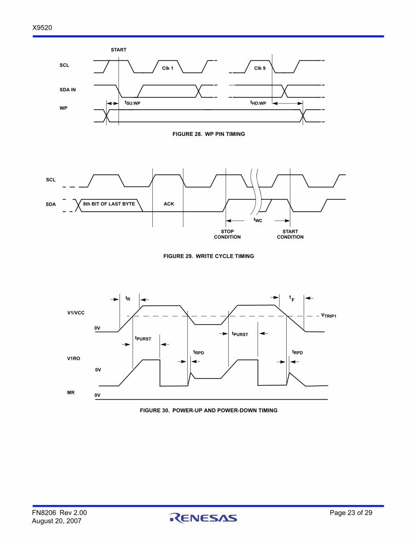
FIGURE 28. WP PIN TIMING
SCL
SDA
tWC
8th BIT OF LAST BYTE ACK
STOP CONDITION
STARTCONDITION
FIGURE 29. WRITE CYCLE TIMING
V1/VCC
tPURST
tR tF
0V
VTRIP1
V1RO
tRPD
0V
tPURST
MR0V
tRPD
FIGURE 30. POWER-UP AND POWER-DOWN TIMING
FN8206 Rev 2.00 Page 23 of 29August 20, 2007

X9520
0V
MR
V1RO
tPURSTtMRD
0V
V1/VCC V1/VCC
V TRIP1
tMRPW
FIGURE 31. MANUAL RESET TIMING DIAGRAM
Vx
tRx
tFx
V TRIPx
VRVALID
VxRO
tRPDx
0V
Note : x = 2,3.0V
0VtRPDx
tRPDx
tRPDx
V TRIP1
V1/VCC
FIGURE 32. V2, V3 TIMING DIAGRAM
FN8206 Rev 2.00 Page 24 of 29August 20, 2007

X9520
WP
tVPS
VP
tVPO
SCL
SDA
twc
tTSU tTHD
V1/VCC, V2, V3
VTRIPx
00h
tVPHNOTE : V1/VCC must be greater than V2, V3 when programming.
FIGURE 33. VTRIPX PROGRAMMING TIMING DIAGRAM (X = 1,2,3)
START
1 0 1 0 1 1 1 0 ACK
WT 0 0 0 0 0 P1 P0 ACK
STOP
ACK
D7 D6 D5 D4 D3 D2 D1 D0
SLAVE ADDRESS BYTE INSTRUCTION BYTE DATA BYTE
SCL
SDA
Time
Rwx (x = 0,1,2)
twr
Rwx(n+1)
Rwx(n-1)
Rwx(n)
n = tap position
FIGURE 34. DCP “WIPER POSITION” TIMING
FN8206 Rev 2.00 Page 25 of 29August 20, 2007

X9520
Appendix 1
DCP1 (100 Tap) Tap Position to Data Byte Translation Table
TAP POSITION
DATA BYTE
DECIMAL BINARY
0 0 0000 0000
1 1 0000 0001
.
...
.
.
23 23 0001 0111
24 24 0001 1000
25 56 0011 1000
26 55 0011 0111
.
...
.
.
48 33 0010 0001
49 32 0010 0000
50 64 0100 0000
51 65 0100 0001
.
...
.
.
73 87 0101 0111
74 88 0101 1000
75 120 0111 1000
76 119 0111 0111
.
...
.
.
98 97 0110 0001
99 96 0110 0000
FN8206 Rev 2.00 Page 26 of 29August 20, 2007

X9520
Appendix 2
DCP1 (100 Tap) Tap Position to Data Byte Translation Algorithm Example. (Example 1)
unsigned DCP1_TAP_Position(int tap_pos){
int block;int i;int offset;int wcr_val;
offset= 0;block = tap_pos / 25;
if (block < 0) return ((unsigned)0);
else if (block <= 3){ switch(block)
{ case (0): return ((unsigned)tap_pos) ;
case (1):{
wcr_val = 56;offset = tap_pos - 25;for (i=0; i<= offset; i++) wcr_val-- ;return ((unsigned)++wcr_val);
}
case (2):{
wcr_val = 64;offset = tap_pos - 50;for (i=0; i<= offset; i++) wcr_val++ ;return ((unsigned)--wcr_val);
}
case (3):{
wcr_val = 120;offset = tap_pos - 75;for (i=0; i<= offset; i++) wcr_val-- ;return ((unsigned)++wcr_val);
}}
}return((unsigned)01100000);
}
FN8206 Rev 2.00 Page 27 of 29August 20, 2007

X9520
Appendix 2
DCP1 (100 TAP) TAP POSITION TO DATA BYTE TRANSLATION ALGORITHM EXAMPLE. (EXAMPLE 2)
unsigned DCP100_TAP_Position(int tap_pos) { /* optional range checking */ if (tap_pos < 0) return ((unsigned)0); /* set to min val */ else if (tap_pos >99) return ((unsigned) 96); /* set to max val */
/* 100 Tap DCP encoding formula */ if (tap_pos > 74) return ((unsigned) (195 - tap_pos)); else if (tap_pos > 49) return ((unsigned) (14 + tap_pos)); else if (tap_pos > 24) return ((unsigned) (81 - tap_pos)); else return (tap_pos); }
FN8206 Rev 2.00 Page 28 of 29August 20, 2007

FN8206 Rev 2.00 Page 29 of 29August 20, 2007
X9520
Intersil products are manufactured, assembled and tested utilizing ISO9001 quality systems as notedin the quality certifications found at www.intersil.com/en/support/qualandreliability.html
Intersil products are sold by description only. Intersil may modify the circuit design and/or specifications of products at any time without notice, provided that such modification does not, in Intersil's sole judgment, affect the form, fit or function of the product. Accordingly, the reader is cautioned to verify that datasheets are current before placing orders. Information furnished by Intersil is believed to be accurate and reliable. However, no responsibility is assumed by Intersil or its subsidiaries for its use; nor for any infringements of patents or other rights of third parties which may result from its use. No license is granted by implication or otherwise under any patent or patent rights of Intersil or its subsidiaries.
For information regarding Intersil Corporation and its products, see www.intersil.com
For additional products, see www.intersil.com/en/products.html
© Copyright Intersil Americas LLC 2005-2007. All Rights Reserved.All trademarks and registered trademarks are the property of their respective owners.
Thin Shrink Small Outline Package Family (TSSOP)
N (N/2)+1
(N/2)
TOP VIEW
AD
0.20 C2X
B A
N/2 LEAD TIPSB
E1E
0.25 C A BM
1
H
PIN #1 I.D.
0.05e
C
0.10 C
N LEADS SIDE VIEW
0.10 C A BMb
c
SEE DETAIL “X”
END VIEW
DETAIL X
A2
0° - 8°
GAUGEPLANE
0.25
LA1
A
L1
SEATINGPLANE
MDP0044THIN SHRINK SMALL OUTLINE PACKAGE FAMILY
SYMBOL 14 LD 16 LD 20 LD 24 LD 28 LD TOLERANCE
A 1.20 1.20 1.20 1.20 1.20 Max
A1 0.10 0.10 0.10 0.10 0.10 ±0.05
A2 0.90 0.90 0.90 0.90 0.90 ±0.05
b 0.25 0.25 0.25 0.25 0.25 +0.05/-0.06
c 0.15 0.15 0.15 0.15 0.15 +0.05/-0.06
D 5.00 5.00 6.50 7.80 9.70 ±0.10
E 6.40 6.40 6.40 6.40 6.40 Basic
E1 4.40 4.40 4.40 4.40 4.40 ±0.10
e 0.65 0.65 0.65 0.65 0.65 Basic
L 0.60 0.60 0.60 0.60 0.60 ±0.15
L1 1.00 1.00 1.00 1.00 1.00 Reference
Rev. E 12/02NOTES:
1. Dimension “D” does not include mold flash, protrusions or gate burrs. Mold flash, protrusions or gate burrs shall not exceed0.15mm per side.
2. Dimension “E1” does not include interlead flash or protrusions. Interlead flash and protrusions shall not exceed 0.25mm perside.
3. Dimensions “D” and “E1” are measured at dAtum Plane H.
4. Dimensioning and tolerancing per ASME Y14.5M-1994.


![[PPT]Fast Ethernet and Gigabit Ethernet - WPIweb.cs.wpi.edu/~rek/Undergrad_Nets/B04/Fast_Ethernet.ppt · Web viewFast Ethernet and Gigabit Ethernet Fast Ethernet (100BASE-T) How to](https://static.fdocuments.net/doc/165x107/5b29d4a97f8b9aad2f8b4e9d/pptfast-ethernet-and-gigabit-ethernet-rekundergradnetsb04fastethernetppt.jpg)