FETs: Field Effect Transistors - Carnegie Mellon Universityee321/spring99/LECT/lect19mar31.pdf ·...
25
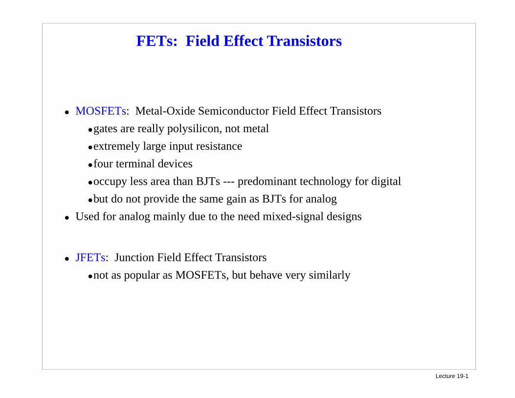
Lecture 19-1 FETs: Field Effect Transistors • MOSFETs: Metal-Oxide Semiconductor Field Effect Transistors •gates are really polysilicon, not metal •extremely large input resistance •four terminal devices •occupy less area than BJTs --- predominant technology for digital •but do not provide the same gain as BJTs for analog • Used for analog mainly due to the need mixed-signal designs • JFETs: Junction Field Effect Transistors •not as popular as MOSFETs, but behave very similarly
Transcript of FETs: Field Effect Transistors - Carnegie Mellon Universityee321/spring99/LECT/lect19mar31.pdf ·...
Lecture 19-1
FETs: Field Effect Transistors
• MOSFETs: Metal-Oxide Semiconductor Field Effect Transistors
• gates are really polysilicon, not metal
• extremely large input resistance
• four terminal devices
• occupy less area than BJTs --- predominant technology for digital
• but do not provide the same gain as BJTs for analog
• Used for analog mainly due to the need mixed-signal designs
• JFETs: Junction Field Effect Transistors
• not as popular as MOSFETs, but behave very similarly
Lecture 19-2
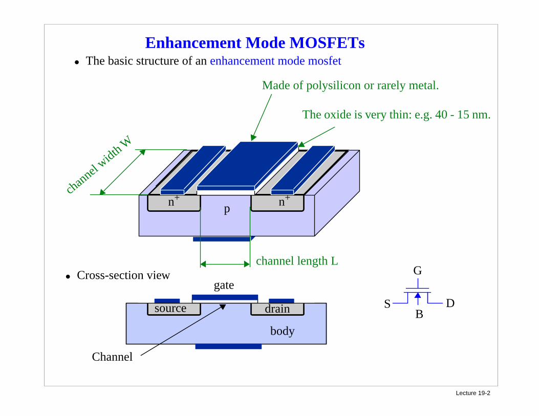
Enhancement Mode MOSFETs
gate
drainsource
body
D
G
B
n+ n+p
• Cross-section view
• The basic structure of an enhancement mode mosfet
Channel
channel length L
channel w
idth W
Made of polysilicon or rarely metal.
The oxide is very thin: e.g. 40 - 15 nm.
S
Lecture 19-3
Enhancement Mode MOSFETs
S
D
GB
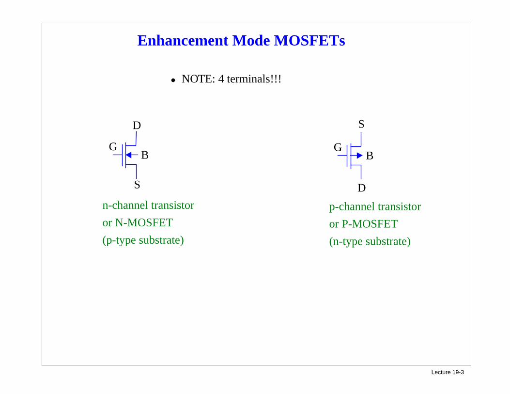
• NOTE: 4 terminals!!!
D
GB
S
n-channel transistor
or N-MOSFET
(p-type substrate)
p-channel transistor
or P-MOSFET
(n-type substrate)
Lecture 19-4
Enhancement Mode MOSFETs
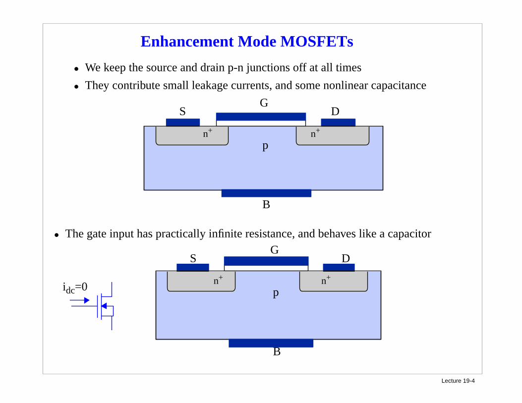
• We keep the source and drain p-n junctions off at all times
• They contribute small leakage currents, and some nonlinear capacitance
• The gate input has practically infinite resistance, and behaves like a capacitor
n+ n+
p
S DG
B
n+ n+
p
S DG
B
idc=0
Lecture 19-5
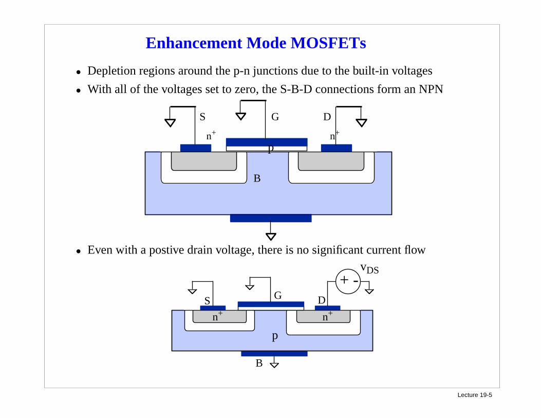
Enhancement Mode MOSFETs
+ -
• Depletion regions around the p-n junctions due to the built-in voltages
• With all of the voltages set to zero, the S-B-D connections form an NPN
B
S DG
n+ n+
p
• Even with a postive drain voltage, there is no significant current flow
B
S DG
n+ n+
p
vDS
Lecture 19-6
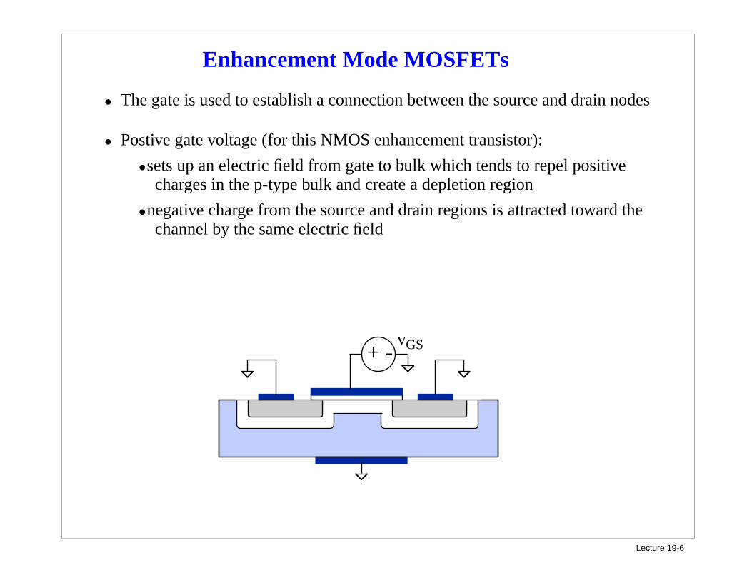
Enhancement Mode MOSFETs
• The gate is used to establish a connection between the source and drain nodes
• Postive gate voltage (for this NMOS enhancement transistor):
• sets up an electric field from gate to bulk which tends to repel positive charges in the p-type bulk and create a depletion region
• negative charge from the source and drain regions is attracted toward the channel by the same electric field
vGS+ -
Lecture 19-7
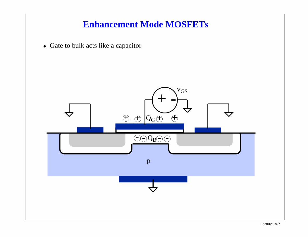
Enhancement Mode MOSFETs
• Gate to bulk acts like a capacitor
+ -
-
+ + + +
- - -QB
QG
p
vGS
Lecture 19-8
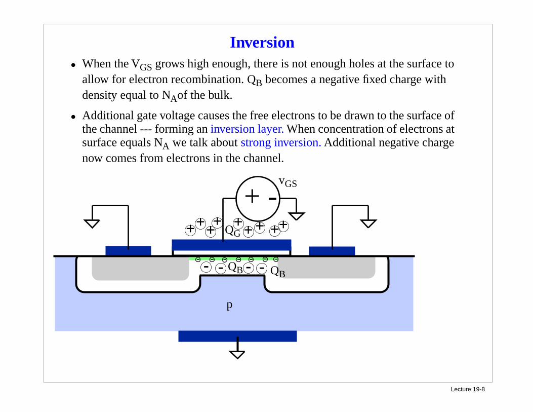
Inversion
+ -
-
+ + + +
- - -QB
QG
p
vGS
QB
- - - - - - -
• When the VGS grows high enough, there is not enough holes at the surface to allow for electron recombination. QB becomes a negative fixed charge with density equal to NAof the bulk.
• Additional gate voltage causes the free electrons to be drawn to the surface of the channel --- forming an inversion layer. When concentration of electrons at surface equals NA we talk about strong inversion. Additional negative charge now comes from electrons in the channel.
+ + + ++
Lecture 19-9
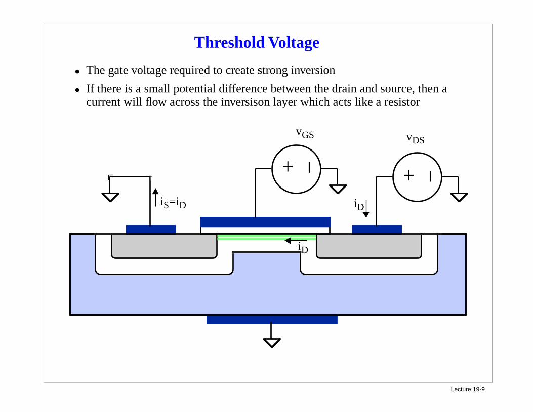
Threshold Voltage
+ - + -
• The gate voltage required to create strong inversion
• If there is a small potential difference between the drain and source, then a current will flow across the inversison layer which acts like a resistor
iD
iDiS=iD
vGS vDS
+ _ + _
Lecture 19-10
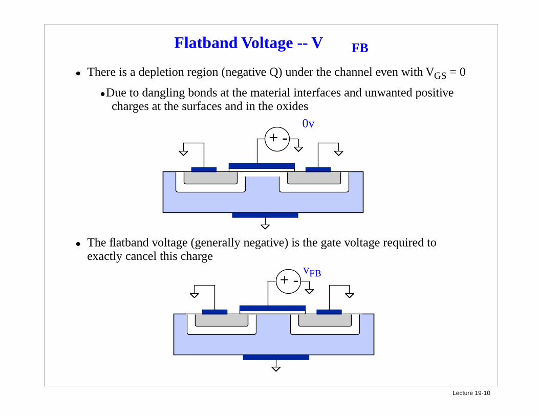
Flatband Voltage -- V FB
• There is a depletion region (negative Q) under the channel even with VGS = 0
• Due to dangling bonds at the material interfaces and unwanted positive charges at the surfaces and in the oxides
• The flatband voltage (generally negative) is the gate voltage required to exactly cancel this charge
+ -
0v
vFB
+ -
Lecture 19-11
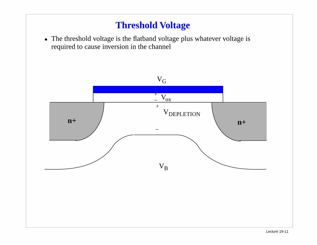
Threshold Voltage• The threshold voltage is the flatband voltage plus whatever voltage is
required to cause inversion in the channel
VB
VG
VDEPLETION+
_n+n+
+_ Vox
Lecture 19-12
Threshold Voltage
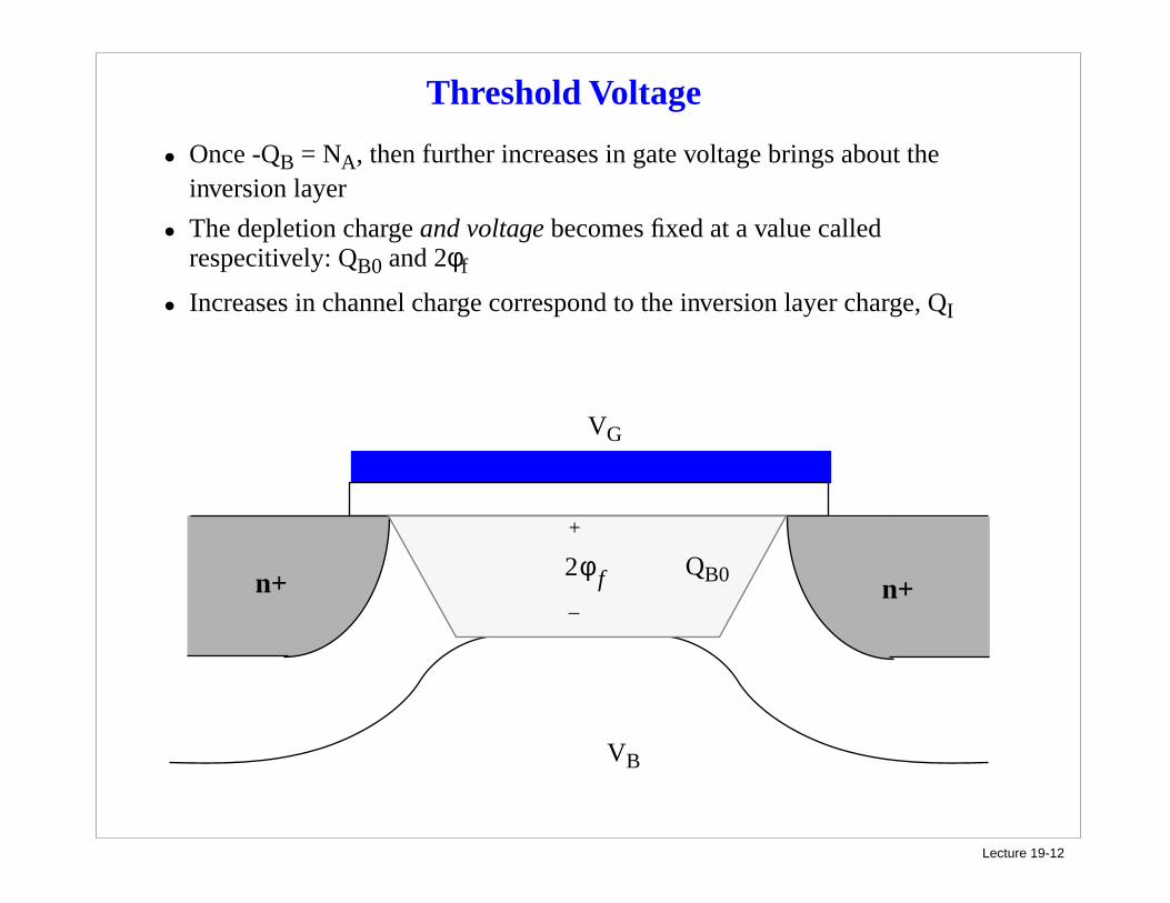
• Once -QB = NA, then further increases in gate voltage brings about the inversion layer
• The depletion charge and voltage becomes fixed at a value called respecitively: QB0 and 2φf
• Increases in channel charge correspond to the inversion layer charge, QI
VB
VG
+
n+n+QB0
+
_
2φf
Lecture 19-13
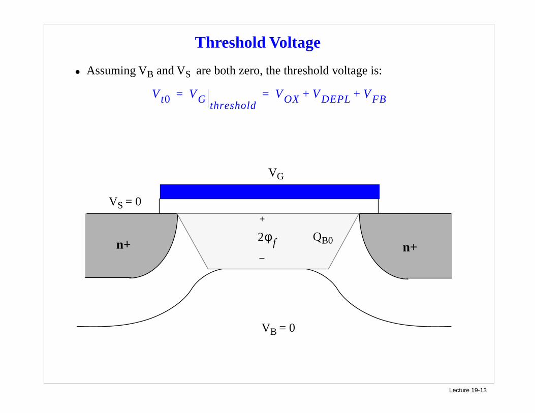
Threshold Voltage
• Assuming VB and VS are both zero, the threshold voltage is:
VB = 0
VG
+
n+n+QB0
+
_
2φf
Vt0 VGthreshold
VOX VDEPL VFB+ += =
VS = 0
Lecture 19-14
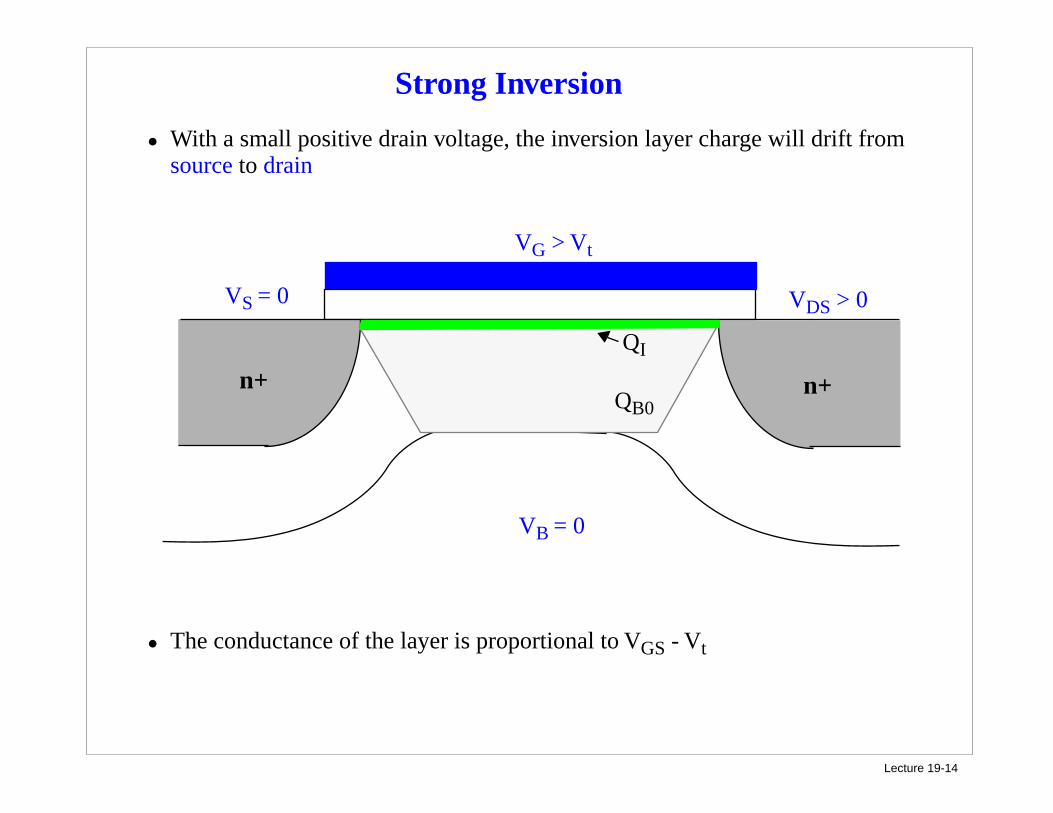
Strong Inversion
• With a small positive drain voltage, the inversion layer charge will drift from source to drain
VB = 0
VG > Vt
+
n+n+QB0
VS = 0
QI
• The conductance of the layer is proportional to VGS - Vt
VDS > 0
Lecture 19-15
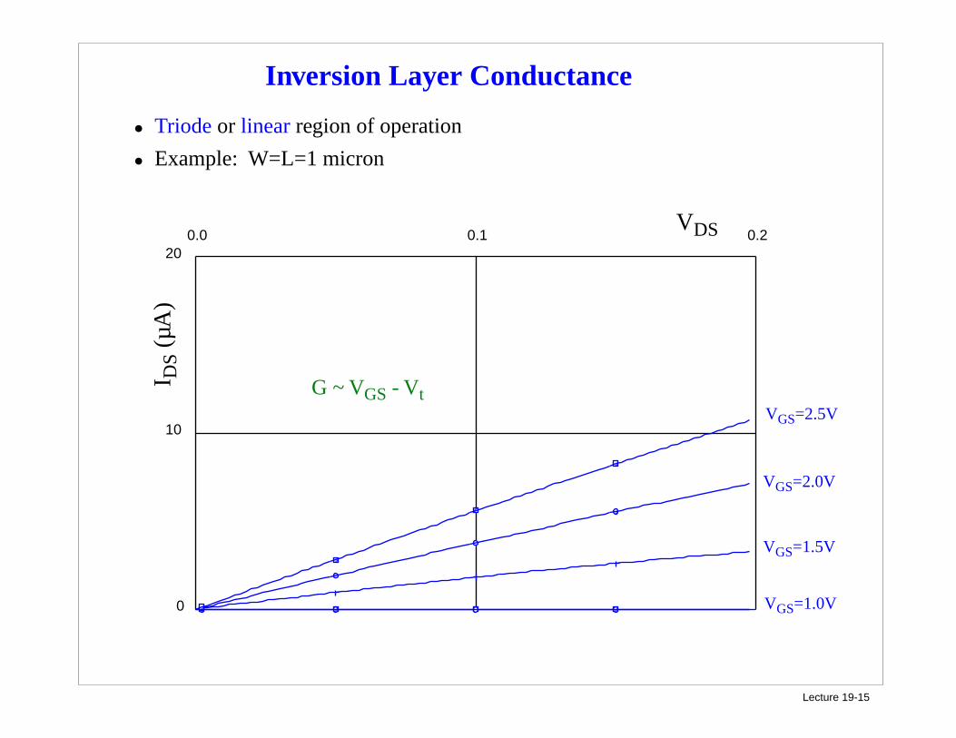
Inversion Layer Conductance
• Triode or linear region of operation
• Example: W=L=1 micron
0.0 0.1 0.2
0
10
20
I DS
(µA
)
VDS
VGS=2.5V
VGS=2.0V
VGS=1.5V
VGS=1.0V
G ~ VGS - Vt
Lecture 19-16
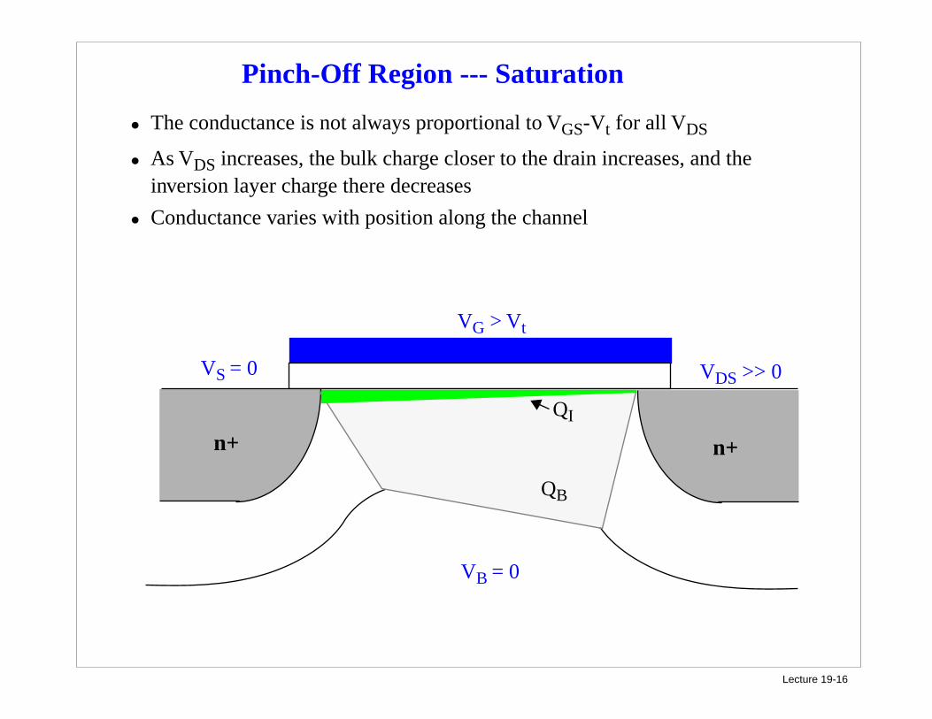
Pinch-Off Region --- Saturation
• The conductance is not always proportional to VGS-Vt for all VDS
• As VDS increases, the bulk charge closer to the drain increases, and the inversion layer charge there decreases
• Conductance varies with position along the channel
VB = 0
VG > Vt
+
n+n+
QB
VS = 0
QI
VDS >> 0
Lecture 19-17
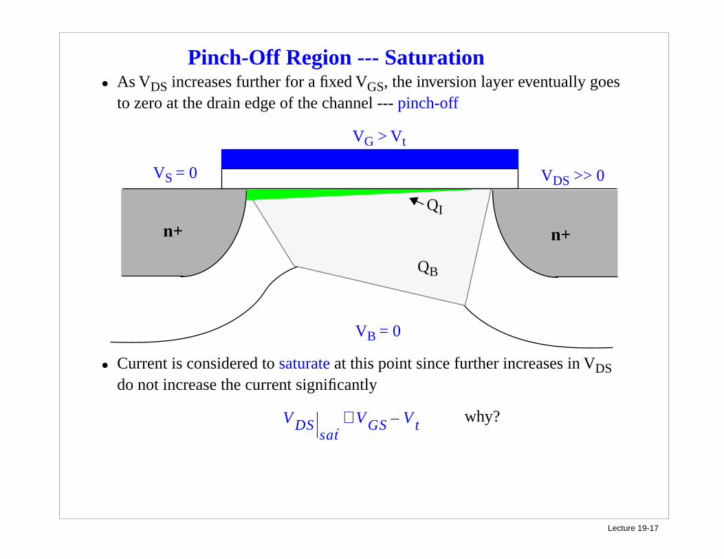
Pinch-Off Region --- Saturation• As VDS increases further for a fixed VGS, the inversion layer eventually goes
to zero at the drain edge of the channel --- pinch-off
VB = 0
VG > Vt
+
n+n+
QB
VS = 0
QI
VDS >> 0
• Current is considered to saturate at this point since further increases in VDS do not increase the current significantly
VDSsat
VGS Vt–≅ why?
Lecture 19-18
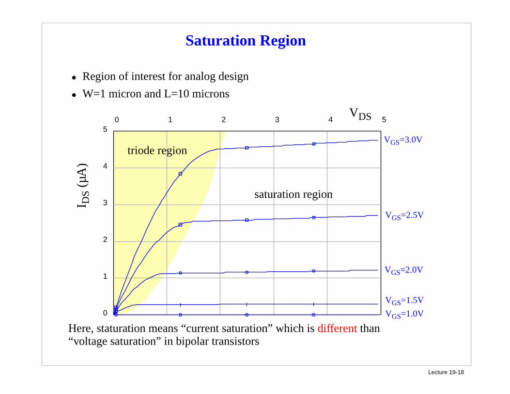
Saturation Region
• Region of interest for analog design
• W=1 micron and L=10 micronsI D
S (µ
A)
VDS
VGS=2.5V
VGS=2.0V
VGS=1.5V
VGS=1.0V
VGS=3.0V
0 1 2 3 4 5
0
1
2
3
4
5
triode region
saturation region
Here, staturation means “current saturation” which is different than “voltage saturation” in bipolar transistors
Lecture 19-19
Equations
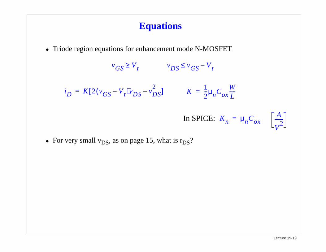
• Triode region equations for enhancement mode N-MOSFET
iD K 2 vGS Vt–( )vDS vDS2
–[ ]=
vGS Vt≥ vDS vGS Vt–≤
K12---µnCox
WL-----=
A
V2
-------
• For very small vDS, as on page 15, what is rDS?
In SPICE: Kn µnCox=
Lecture 19-20
Equations
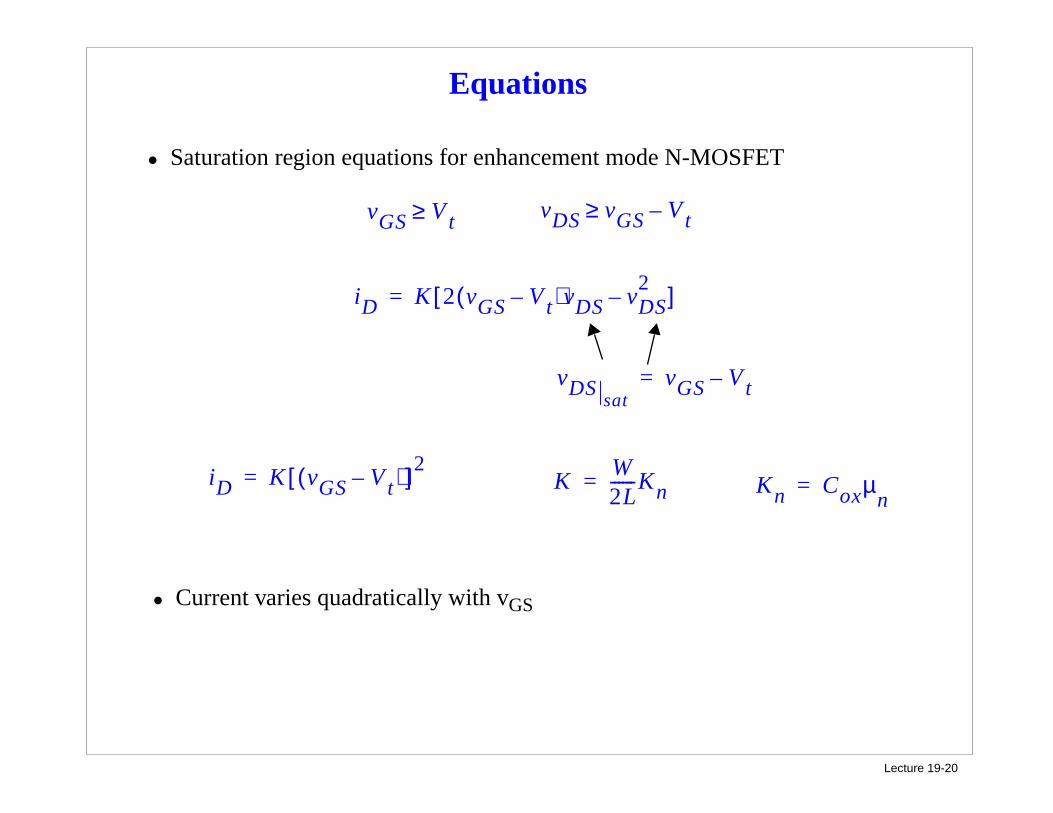
• Saturation region equations for enhancement mode N-MOSFET
iD K 2 vGS Vt–( )vDS vDS2
–[ ]=
vGS Vt≥ vDS vGS Vt–≥
vDSsat
vGS Vt–=
• Current varies quadratically with vGS
iD K vGS Vt–( )[ ] 2= K
W2L------Kn= Kn Coxµn
=
Lecture 19-21
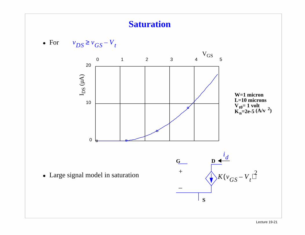
Saturation
• For vDS vGS Vt–≥
0 1 2 3 4 5
0
10
20
I DS
(µA
)
VGS
• Large signal model in saturation
id
S
G D
K vGS Vt–( )2+
_
W=1 micronL=10 micronsV t0= 1 voltK n=2e-5 (A/v 2)
Lecture 19-22
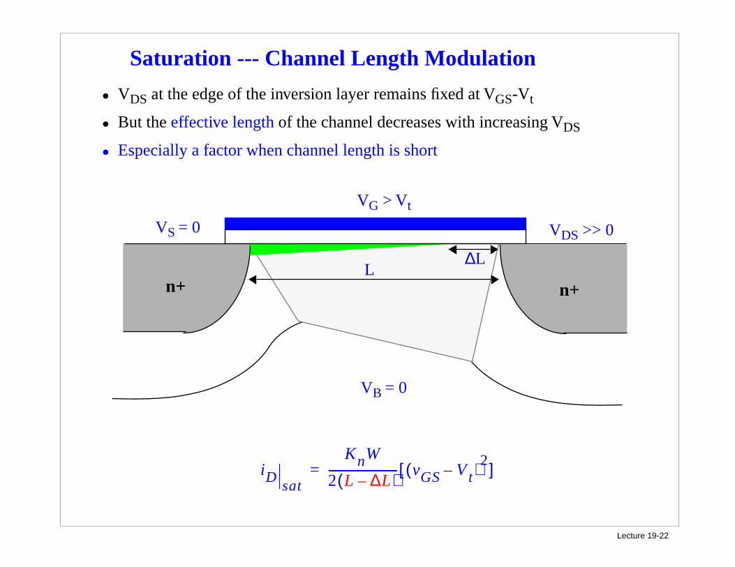
Saturation --- Channel Length Modulation
• VDS at the edge of the inversion layer remains fixed at VGS-Vt
• But the effective length of the channel decreases with increasing VDS
• Especially a factor when channel length is short
VB = 0
VG > Vt
+
n+n+
VS = 0 VDS >> 0
L∆L
iDsat
KnW
2 L ∆L–( )------------------------- vGS Vt–( )2[ ]=
Lecture 19-23
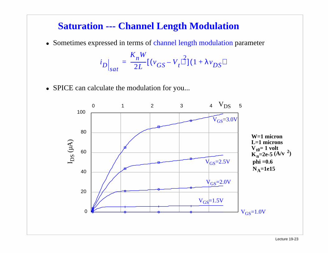
Saturation --- Channel Length Modulation
• Sometimes expressed in terms of channel length modulation parameter
iDsat
KnW
2L------------- vGS Vt–( )2[ ] 1 λvDS+( )=
0 1 2 3 4 5
0
20
40
60
80
100
W=1 micronL=1 micronsV t0= 1 voltK n=2e-5 (A/v 2)phi =0.6NA=1e15
I DS
(µA
)
VDS
VGS=2.5V
VGS=2.0V
VGS=1.5V
VGS=1.0V
VGS=3.0V
• SPICE can calculate the modulation for you...
Lecture 19-24
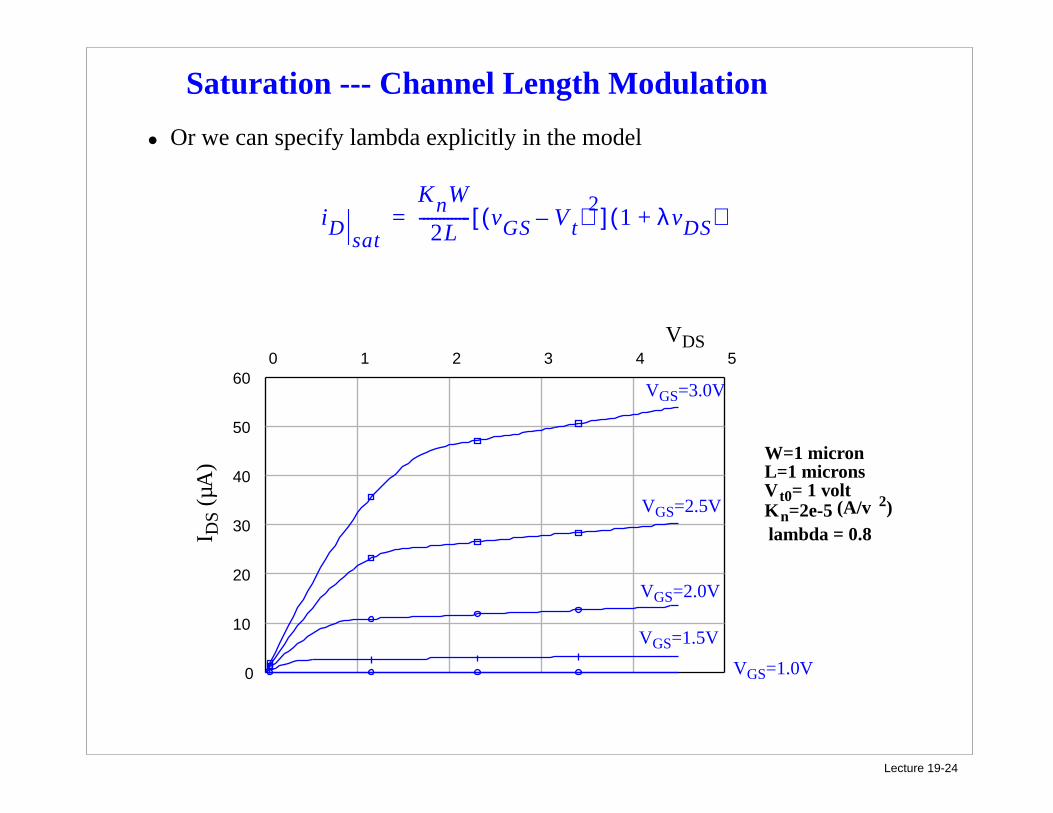
Saturation --- Channel Length Modulation
• Or we can specify lambda explicitly in the model
iDsat
KnW
2L------------- vGS Vt–( )2[ ] 1 λvDS+( )=
W=1 micronL=1 micronsV t0= 1 voltK n=2e-5 (A/v 2)lambda = 0.8I D
S (µ
A)
VDS
VGS=2.5V
VGS=2.0V
VGS=1.5V
VGS=1.0V
VGS=3.0V
0 1 2 3 4 5
0
10
20
30
40
50
60
Lecture 19-25
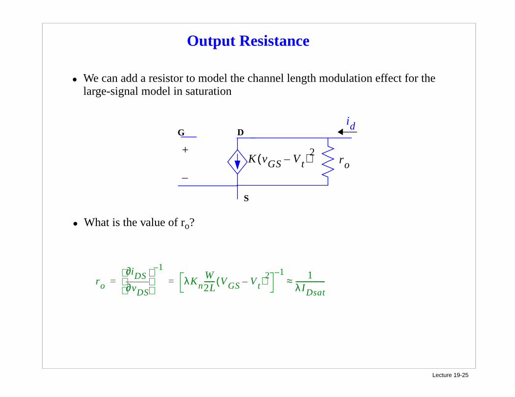
Output Resistance
• We can add a resistor to model the channel length modulation effect for the large-signal model in saturation
id
S
G D
K vGS Vt–( )2+
_
• What is the value of ro?
ro
ro vDS∂∂iDS
1–
λKnW2L------ VGS Vt–( )2
1– 1λ I Dsat-----------------≈= =