Ferromagnetism in Rhombohedral Trilayer Graphene
53
University of California Santa Barbara Ferromagnetism in Rhombohedral Trilayer Graphene Strongly correlated electrons in ABC trilayer/hexagonal boron nitride heterostructures A dissertation submitted in partial satisfaction of the requirements for the degree Bachelor of Science in Physics by Tian Xie Committee in charge: Professor Andrea Young, Research Advisor, Chair Spring 2021
Transcript of Ferromagnetism in Rhombohedral Trilayer Graphene
University of CaliforniaSanta Barbara
Ferromagnetism in Rhombohedral Trilayer Graphene
Strongly correlated electrons in ABC trilayer/hexagonal boron nitride
heterostructures
A dissertation submitted in partial satisfaction
of the requirements for the degree
Bachelor of Science
in
Physics
by
Tian Xie
Committee in charge:
Professor Andrea Young, Research Advisor, Chair
Spring 2021
The Dissertation of Tian Xie is approved.
Professor Andrea Young, Research Advisor, Committee Chair
Spring 2021
Abstract
Ferromagnetism in Rhombohedral Trilayer Graphene
Strongly correlated electrons in ABC trilayer/hexagonal boron nitride heterostructures
by
Tian Xie
Trilayer graphene is a two-dimensional electron system consisting of three layers of
honeycomb carbon lattice. Depending on the stacking order, two polytypes, bernal
(ABA) and rhombohedral (ABC) exist in trilayer graphene. The two polytypes are opti-
cally identical but have distinct electronic properties. The ABC-stacked trilayer graphene
has a near flatly dispersion relation in the low energy regime. This unique energy band
structure provides an excellent platform to study electron-electron correlation effects,
which are usually negligible in other two-dimensional electron systems, where single-
electron kinetic energy dominates the electronic properties. Multiple correlation effects
have been reported in ABC-stacked trilayer graphene / hexagonal boron nitride(hBN)
moire superlattices.[1]
In this work, we fabricated ABC-trilayer graphene/hBN heterostructures. Multiple tech-
niques have been applied to identify, isolate, and preserve the ABC-stacked domains
in mechanically exfoliated trilayer graphene. The electronic properties of ABC-trilayer
graphene are characterized by cryogenic electronic transport and capacitance measure-
ment with an adjustable steady magnetic field. We observed electronic incompressible
states at certain carrier densities, consistent with the previous works[1]. We also find that
correlation-induced symmetry breaking happens in ABC-trilayer graphene even without
a moire superlattice.
iii
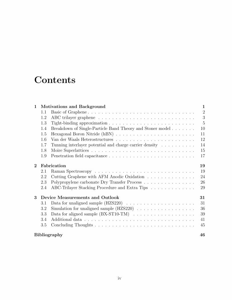
Contents
1 Motivations and Background 11.1 Basic of Graphene . . . . . . . . . . . . . . . . . . . . . . . . . . . . . . . 21.2 ABC trilayer graphene . . . . . . . . . . . . . . . . . . . . . . . . . . . . 31.3 Tight-binding approximation . . . . . . . . . . . . . . . . . . . . . . . . . 51.4 Breakdown of Single-Particle Band Theory and Stoner model . . . . . . . 101.5 Hexagonal Boron Nitride (hBN) . . . . . . . . . . . . . . . . . . . . . . . 111.6 Van der Waals Heterostructures . . . . . . . . . . . . . . . . . . . . . . . 121.7 Tunning interlayer potential and charge carrier density . . . . . . . . . . 141.8 Moire Superlattices . . . . . . . . . . . . . . . . . . . . . . . . . . . . . . 151.9 Penetration field capacitance . . . . . . . . . . . . . . . . . . . . . . . . . 17
2 Fabrication 192.1 Raman Spectroscopy . . . . . . . . . . . . . . . . . . . . . . . . . . . . . 192.2 Cutting Graphene with AFM Anodic Oxidation . . . . . . . . . . . . . . 242.3 Polypropylene carbonate Dry Transfer Process . . . . . . . . . . . . . . . 262.4 ABC-Trilayer Stacking Procedure and Extra Tips . . . . . . . . . . . . . 29
3 Device Measurements and Outlook 313.1 Data for unaligned sample (HZS220) . . . . . . . . . . . . . . . . . . . . 313.2 Simulation for unaligned sample (HZS220) . . . . . . . . . . . . . . . . . 363.3 Data for aligned sample (BX-ST10-TM) . . . . . . . . . . . . . . . . . . 393.4 Additional data . . . . . . . . . . . . . . . . . . . . . . . . . . . . . . . . 413.5 Concluding Thoughts . . . . . . . . . . . . . . . . . . . . . . . . . . . . . 45
Bibliography 46
iv
Acknowledgements
I’d like to first thank Haoxin Zhou who mentored me on this project, as well as my
research advisor Andrea Young for his guidance. I’d also like to thank Areg Ghazaryan
and Maksym Serbyn in Institute of Science and Technology Austria for their great support
on theoretical modelling and simulation for the ABC trilayer graphene system.
v
Chapter 1
Motivations and Background
In 2004, graphene is first discovered by Andre Geim through mechanical exfoliation [2].
Followed by observation of quantum Hall effect, similar to other 2D electron gas systems
such as GaAs, with significant gate tunability [3].
These novel observations attract many scientists coming to work in these field, and var-
ious fabrication technics have mushroomed. For example, innovation of the hexagonal
boron nitride (hBN) encapsulation method during graphene sample fabrication allows
us to decrease the disorder in graphene devices. At the same time, the excellent prop-
erties of hBN also enable us fabricating a much more complicated device by using it
as a 2-D insulator to lower disorder in graphene sample [4]. On the other hand, the
pc/ppc dry transfer technics also increase the efficiency to produce for complicated Van
der Waals heterostructures fabrication [5]. Moreover, people realize the dual graphite
gate devices can significantly suppress disorder caused by the gates and allow them to
probe fragile phenomena that are absent in metal gated devices [32]. Under all the sup-
port of these technics, condensed matter experimentalists can now fabricate graphene
device with quality that is comparable to GaAs samples and also allows them to detailly
study the interesting correlation effect happens in multilayer graphene system such as
1
Motivations and Background Chapter 1
fractional quantum hall effect in bilayer graphene and the famous superconducting state
in twisted bilayer graphene (tBLG) [6, 7].
But besides the bilayer system, recent studies on rhombohedral multilayer graphene both
with and without moire have also shown many interesting correlation effects such as
magneto hysteresis in ABC trilayer graphene [8]; spontaneous gap opening in multilayer
graphene [9]; gate tunable ferromagnetism in ABCA graphene [10], and even signatures
of superconductivity [1]. All these exciting observation indicate that the rhombohedral
multilayer graphene system is worth further investigation. Different from tBLG or other
twisted heterostructures with angle disorder, the homogeneity in rhombohedral multi-
layer graphene, hBN Van der Waals heterostructures, allows us to measure the accurate
penetration field capacitance enables us to obtain both bulk and edge behavior by com-
paring its transport and capacitance data.
1.1 Basic of Graphene
Graphene is a two-dimensional sheet of carbon atoms arranged in a hexagonal lattice.
Each carbon atom has four valence electron 2s,2px,2py,2pz. The three electrons in 2s and
2px and 2py orbit will undergo sp2 hybridized [12] and forms strong in-plane σ-bonding to
three other neighboring atoms. The fourth electron in 2pz is left in the vertical direction
and forms an out plane π-bond. As the π-bond is a more diffusive bond compared to
the σ-bond, it contributes most to the electronic properties of graphene. When using
a tight-binding model to calculate low energy band structure for graphene, a cone-like
structure can be observed, which is normally referred to as Dirac cone.
2
Motivations and Background Chapter 1
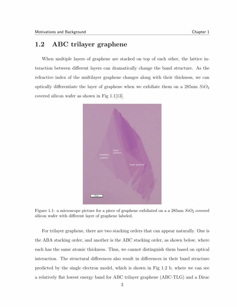
1.2 ABC trilayer graphene
When multiple layers of graphene are stacked on top of each other, the lattice in-
teraction between different layers can dramatically change the band structure. As the
refractive index of the multilayer graphene changes along with their thickness, we can
optically differentiate the layer of graphene when we exfoliate them on a 285nm SiO2
covered silicon wafer as shown in Fig 1.1[13].
Figure 1.1: a microscope picture for a piece of graphene exfoliated on a a 285nm SiO2 coveredsilicon wafer with different layer of graphene labeled.
For trilayer graphene, there are two stacking orders that can appear naturally. One is
the ABA stacking order, and another is the ABC stacking order, as shown below, where
each has the same atomic thickness. Thus, we cannot distinguish them based on optical
interaction. The structural differences also result in differences in their band structure
predicted by the single electron model, which is shown in Fig 1.2 b, where we can see
a relatively flat lowest energy band for ABC trilayer graphene (ABC-TLG) and a Dirac
3
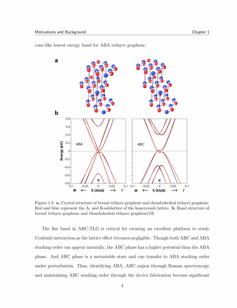
Motivations and Background Chapter 1
cone-like lowest energy band for ABA trilayer graphene.
Figure 1.2: a, Crystal structure of bernal trilayer graphene and rhombohedral trilayer graphene.Red and blue represent the A- and B-sublattice of the honeycomb lattice. b, Band structure ofbernal trilayer graphene and rhombohedral trilayer graphene[19]
The flat band in ABC-TLG is critical for creating an excellent platform to study
Coulomb interaction as the lattice effect becomes negligible. Though both ABC and ABA
stacking order can appear naturally, the ABC phase has a higher potential than the ABA
phase. And ABC phase is a metastable state and can transfer to ABA stacking order
under perturbation. Thus, identifying ABA, ABC region through Raman spectroscopy
and maintaining ABC stacking order through the device fabrication become significant
4
Motivations and Background Chapter 1
for us, which will be discussed in later chapters.
1.3 Tight-binding approximation
1.3.1 General theory
Determining the energy for electrons in a crystal is always an essential for condense
matter physicist to understand bulk material properties. Under Born-Oppenheimer ap-
proximation, the Hamiltonian for a solid can be simply written as:
H =∑n
p2n2mn
+1
2
∑n
qnqn′
|rn − rn′|(1.1)
Here, the Hamiltonian simply sum over every electron in the lattice and account for
every particle-particle Coulomb interaction. However, it is impossible to find the exact
wave function for from this Hamiltonian since the Schrodinger equation has no general
solution when involving more than one proton’s potential into the equation. Thus, setting
up a model with a good approximation of electrons’ actual behavior becomes significant.
One of the famous approximations is called the tight-binding model from Robert Mul-
liken, where he neglects coulomb interaction and only considers the potential from nuclei
to one electron as the nuclei’s potential is much greater than coulomb energy [15]. Then
assumes the atom that the electron closest to as the major potential source and all other
atoms’ potential as perturbation where the perturbation is just linear superposition for
the nearest neighbor atoms. The Hamiltonian for tight-binding approximation can be
then written as follows:
H = − p2
2m+ V (r − rn) +
∑m 6=n
V (r − rm) (1.2)
5
Motivations and Background Chapter 1
This model allows us to approximate and graph the energy-momentum relationship
of a single electron in a crystal, which is usually referred as band structure. Since the
model neglects electron-electron interaction, the result from many electrons would be the
same as the single electron’s result. The ‘filling’ of these electron bands corresponds to
differences in metallic and insulating behavior for a material.
1.3.2 Monolayer graphene
Since graphene is made of carbon, we can assume that the electron will only have a
circular orbit at each lattice site. Then in real space, when considering the Hamiltonian
for the lattice in matrix form, we get 〈j|H|j± 1〉 = 〈j± 1|H|j〉∗ = C2 and 〈j|H|j〉 = C1,
assuming the crystal lattice holds translational symmetry. By Fourier transformation,
we can calculate the element for the Hamiltonian matrix in momentum space, which has
the form shown below.
H =
C1 C2ei∑
j~K· ~Rij
C∗2e−i
∑j~K· ~Rij C1
(1.3)
Where Rij is the distance between an atom and its nearest neighbors, a further
estimation can be done by Taylor expend the exponential term and only keeping the
linear terms. Then, H(K) can be simplified to
H =
C1 C2
∑jKxj − iKyj
C∗2∑
jKxj + iKyj C1
(1.4)
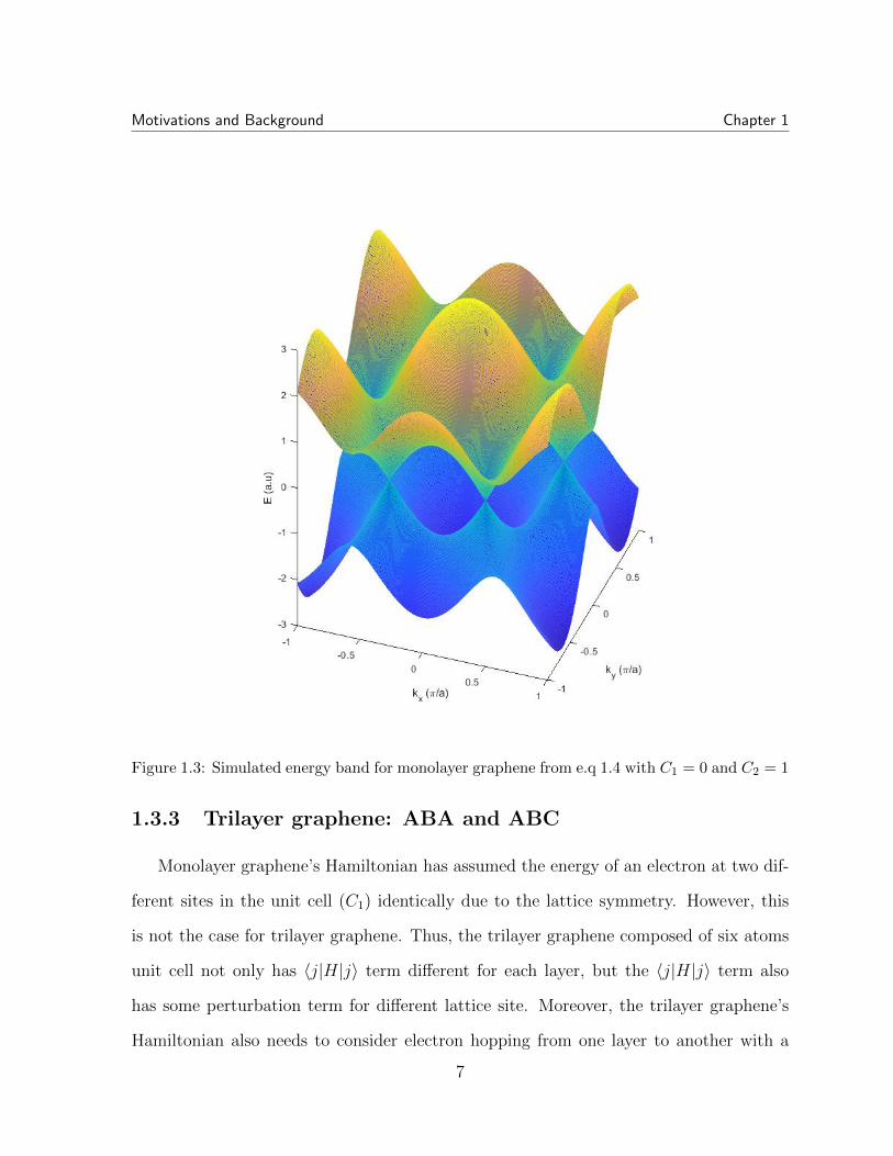
Then, we can plot the energy v.s. momentum plot as shown Fig 1.3.
6
Motivations and Background Chapter 1
Figure 1.3: Simulated energy band for monolayer graphene from e.q 1.4 with C1 = 0 and C2 = 1
1.3.3 Trilayer graphene: ABA and ABC
Monolayer graphene’s Hamiltonian has assumed the energy of an electron at two dif-
ferent sites in the unit cell (C1) identically due to the lattice symmetry. However, this
is not the case for trilayer graphene. Thus, the trilayer graphene composed of six atoms
unit cell not only has 〈j|H|j〉 term different for each layer, but the 〈j|H|j〉 term also
has some perturbation term for different lattice site. Moreover, the trilayer graphene’s
Hamiltonian also needs to consider electron hopping from one layer to another with a
7
Motivations and Background Chapter 1
similar format to the nearest neighbor. But since hopping between layers is not really
momentum dependent, instead layer dependent, the z-direction hoping terms should be
two different constants for electron hopping by one or two layers. With these constraints
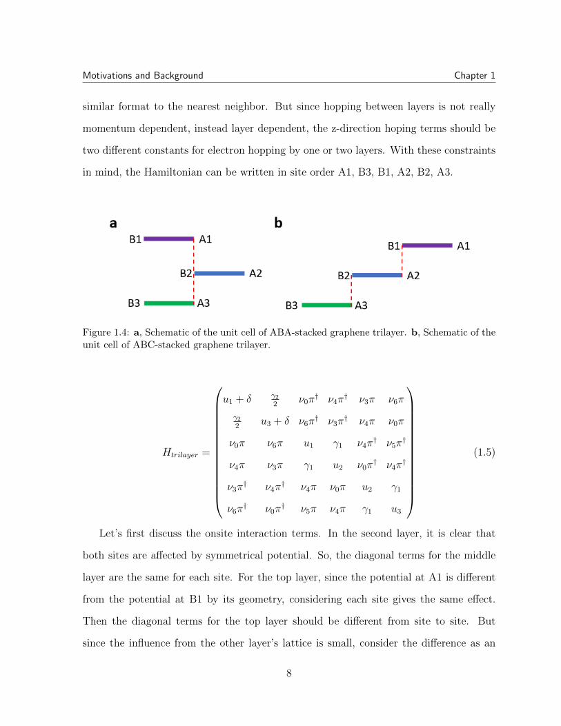
in mind, the Hamiltonian can be written in site order A1, B3, B1, A2, B2, A3.
Figure 1.4: a, Schematic of the unit cell of ABA-stacked graphene trilayer. b, Schematic of theunit cell of ABC-stacked graphene trilayer.
Htrilayer =
u1 + δ γ22
ν0π† ν4π
† ν3π ν6π
γ22
u3 + δ ν6π† ν3π
† ν4π ν0π
ν0π ν6π u1 γ1 ν4π† ν5π
†
ν4π ν3π γ1 u2 ν0π† ν4π
†
ν3π† ν4π
† ν4π ν0π u2 γ1
ν6π† ν0π
† ν5π ν4π γ1 u3
(1.5)
Let’s first discuss the onsite interaction terms. In the second layer, it is clear that
both sites are affected by symmetrical potential. So, the diagonal terms for the middle
layer are the same for each site. For the top layer, since the potential at A1 is different
from the potential at B1 by its geometry, considering each site gives the same effect.
Then the diagonal terms for the top layer should be different from site to site. But
since the influence from the other layer’s lattice is small, consider the difference as an
8
Motivations and Background Chapter 1
additional perturbation term. A similar argument can also apply to the bottom layer’s
diagonal term.
Since only considering the nearest neighbors, the ν5 and ν6 terms vanish from geometric
constraints. The remaining terms are measured by the experimentalist and construct the
final Hamiltonian shown in e.q. 1.6 and 1.7, where the ∆1 is the term for the interlayer
potential tuned by external electric field [11].
H =
∆1 + ∆2 + δ γ22
ν0π† ν4π
† ν3π 0
γ22
−∆1 + ∆2 + δ 0 ν3π† ν4π ν0π
ν0π 0 ∆1 + ∆2 γ1 ν4π† 0
ν4π ν3π γ1 −2∆2 ν0π† ν4π
†
ν3π† ν4π
† ν4π ν0π −2∆2 γ1
0 ν0π† 0 ν4π γ1 −∆1 + ∆2
(1.6)
γ0 γ1 γ2 γ3 γ4 δ ∆2
3.1a 0.38a −0.015 −0.29a −0.141a −0.01015 −0.0023
π = ξKx + iky, νi =
√3aγi2
(1.7)
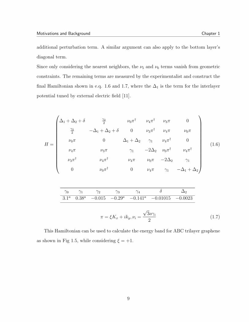
This Hamiltonian can be used to calculate the energy band for ABC trilayer graphene
as shown in Fig 1.5, while considering ξ = +1.
9
Motivations and Background Chapter 1
Figure 1.5: Simulated energy band for ABC graphene with and without external electric fieldby e.q 1.6.
1.4 Breakdown of Single-Particle Band Theory and
Stoner model
As discussed in the previous section, the tight-binding model could explain a large
variety of physic phenomena when lattice potential dominates. However, as the tight-
binding model neglect electron-electron interaction, the Single-Particle model becomes
inaccurate when coulomb interaction makes a significant donation towards the bulk be-
havior of studied material, which is exactly the type of phenomena that are the focus in
this study.
However, the tight-binding model still gives us an excellent foundation to design our
experiment. As the model approximated most of the donation from lattice structure,
finding a relatively flat band will allow us to focus our study on coulomb interaction
10
Motivations and Background Chapter 1
while not disturbed by the effect of the lattice.
After the single-particle band theory, physicists developed many models to describe the
Coulomb interaction. One of the most straightforward models people developed to ex-
plain interaction in metal is the Stoner model [16]. Instead of giving Hamiltonian for
the system, the stoner model directly stated the energy formula for a single electron in
the system while only consider electron has interaction when they have a different flavor.
And we get the formula as below:
E =∑α
E0(µα) +Ua2
2
∑α 6=β
nαnβ (1.8)
Where U is the strength of interaction, E0 is just the electron’s energy in single-
particle band theory, nα and nβ are different flavors of the electron, which can be any
parameter related to the electron. If U=∞ then all the electrons in the system will be
forced into one flavor, and when U=0, all electrons in the system should be distributed
equally to each flavor.
1.5 Hexagonal Boron Nitride (hBN)
Boron nitride is a thermally and chemically resistant refractory compound of boron
and nitrogen with the chemical formula BN [35]. It exists in various crystalline forms that
are isoelectronic to a similarly structured carbon lattice. The most stable crystalline form
is the hexagonal one, also called hBN. Hexagonal boron nitride has a lattice structure
similar to graphite.
Within each layer, boron and nitrogen atoms form strong covalent bonding in the
xy-plane, whereas the layers are held together by weak van der Waals forces. Because of
the polarity of the B–N bonds, the boron atoms are lying over and above nitrogen atoms.
11
Motivations and Background Chapter 1
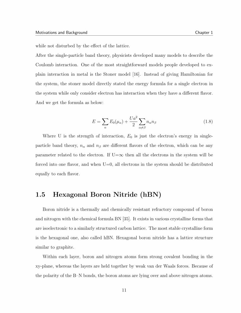
Figure 1.6: a 100x magnification microscope picture for a piece of hBN exfoliated on a 285nmSiO2 covered silicon wafer with thickness around 30nm
hBN has less thermal expansion as well as high uniformity and electrical resistivity.
Moreover, its hexagonal atomic structure has a minimal lattice mismatch with graphene
(around 2%). Owing to these properties, it is often used as the dielectric for graphene
encapsulation to lower disorder in graphene samples [4]. Like graphene, we can also
exfoliate them on a 285nm SiO2 covered silicon wafer and optically differentiate their
thickness through color as shown in Fig 1.6.
1.6 Van der Waals Heterostructures
Most of the interesting behaviors from Coulomb interactions are very delicate; thus,
suppressing the disorder in ABC-TLG becomes significant for detecting its interesting
electronic properties. The innovation of the van der Waals heterostructure has allowed
for unprecedented isolation and measurement of these materials. A Van der Waals het-
12
Motivations and Background Chapter 1
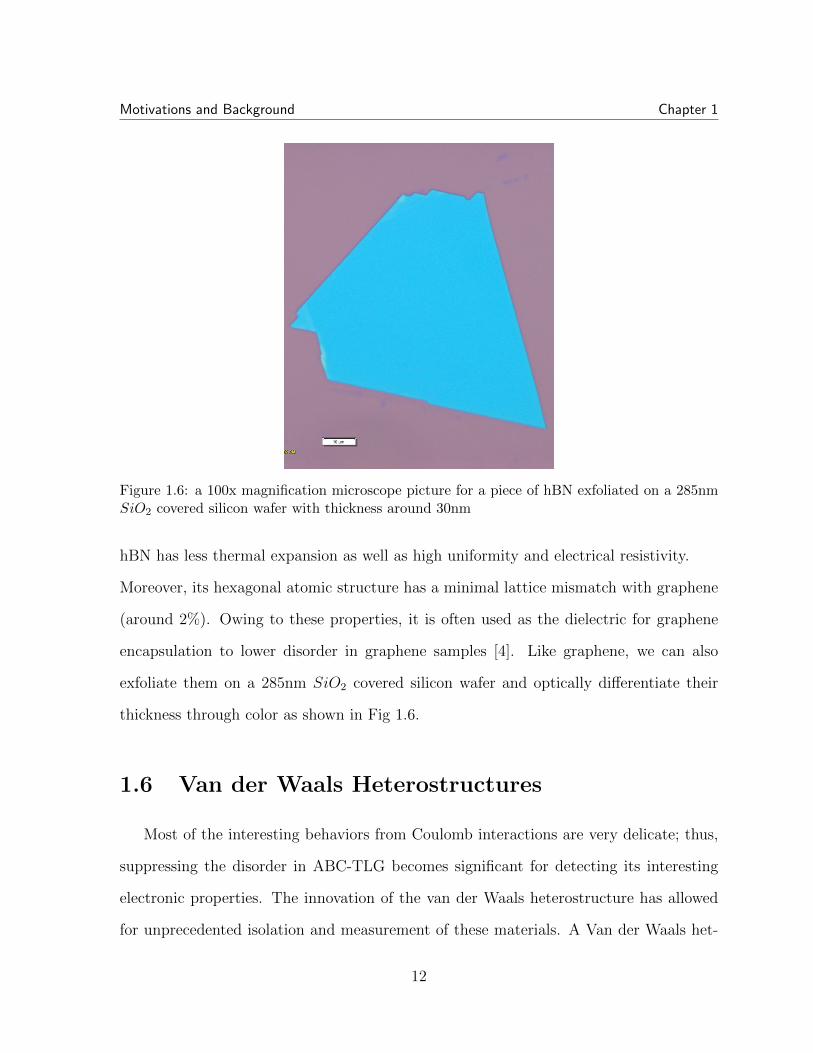
erostructure means jointing different 2-D materials on top of each other by Van der Waals
force and encapsulate the material of interest to suppress disorder with nano-fabrication
techniques. And the most basic structure is just to use two homogeneous insulating
materials to encapsulate the material of interest from two conducting materials that are
sandwiched on top and bottom of the device as shown below, where we generally call
these conducting materials top and bottom gate. This structure allows us to apply a
perpendicular displacement field and control the charge carrier density for the study ma-
terial by applying voltage on top and bottom gates. A basic schematic of this can be seen
in the figure below. In many graphene-based devices, hexagonal boron nitride (hBN) is
used as the encapsulating insulator [4] due to its surface cleanliness and lattice similarity.
Though metal top gate/ silicon bottom gate is widely used in the past few years, there
are also studies have [17] shown that dual graphite gate device could lead to significantly
lower disorder device. A basic schematic of this device can be seen in the Fig 1.7.
Figure 1.7: a 3D schematic of a finished Van der Waals Heterostructures sample
13
Motivations and Background Chapter 1
1.7 Tunning interlayer potential and charge carrier
density
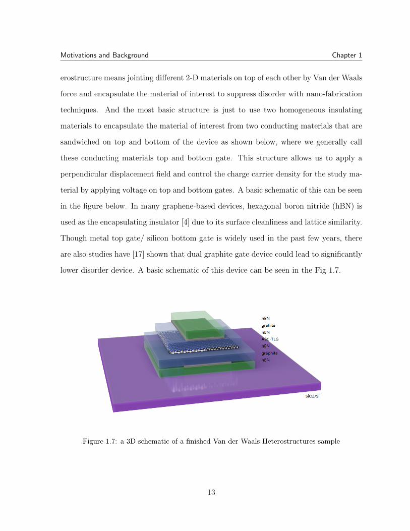
Generally, we will wire our sample in schemata in Fig 1.8 a. Then, when we apply
the same DC voltage to both the top and bottom gates, our ABC trilayer graphene will
have voltage differences compared to its surroundings. Since ABC trilayer graphene is
usually metallic, we can treat it like metal. Then the voltage difference will drive ABC
to suck charge from the ground and increase the charge carrier density in the sample.
Figure 1.8: a, simple schematic for the circuit. b, electron in trilayer graphene with and withoutexternal displacement field
On the other hand, when we apply positive DC voltage to the top and negative DC
voltage bottom gate as schemata below, the voltage difference between the top layer of
ABC and the bottom layer of ABC will be different, forcing electrons to tend to stay at
top layer for ABC. This effect is identical to increasing the interlayer potential for the
bottom layer and decrease the interlayer potential for the top layer.
When the thickness of the two insulators is the same, the displacement field (D) and
14
Motivations and Background Chapter 1
charge carrier density (n0) can be easily calculated by e.q. 1.10.
n0 ∝ VT + VB
D ∝ VT − VB(1.9)
where VT and VB are the top and bottom gate voltages, respectively.
1.8 Moire Superlattices
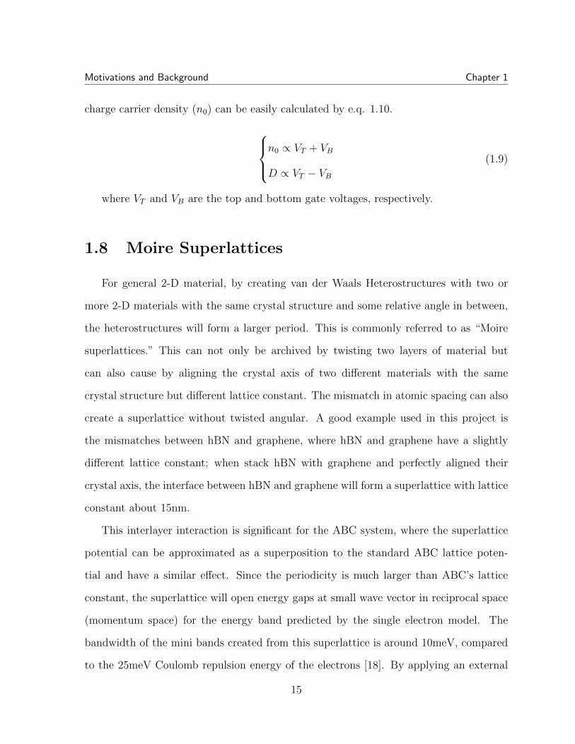
For general 2-D material, by creating van der Waals Heterostructures with two or
more 2-D materials with the same crystal structure and some relative angle in between,
the heterostructures will form a larger period. This is commonly referred to as “Moire
superlattices.” This can not only be archived by twisting two layers of material but
can also cause by aligning the crystal axis of two different materials with the same
crystal structure but different lattice constant. The mismatch in atomic spacing can also
create a superlattice without twisted angular. A good example used in this project is
the mismatches between hBN and graphene, where hBN and graphene have a slightly
different lattice constant; when stack hBN with graphene and perfectly aligned their
crystal axis, the interface between hBN and graphene will form a superlattice with lattice
constant about 15nm.
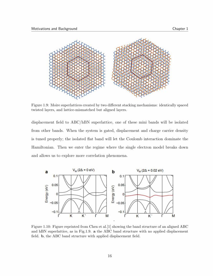
This interlayer interaction is significant for the ABC system, where the superlattice
potential can be approximated as a superposition to the standard ABC lattice poten-
tial and have a similar effect. Since the periodicity is much larger than ABC’s lattice
constant, the superlattice will open energy gaps at small wave vector in reciprocal space
(momentum space) for the energy band predicted by the single electron model. The
bandwidth of the mini bands created from this superlattice is around 10meV, compared
to the 25meV Coulomb repulsion energy of the electrons [18]. By applying an external
15
Motivations and Background Chapter 1
Figure 1.9: Moire superlattices created by two different stacking mechanisms: identically spacedtwisted layers, and lattice-mismatched but aligned layers.
displacement field to ABC/hBN superlattice, one of these mini bands will be isolated
from other bands. When the system is gated, displacement and charge carrier density
is tuned properly; the isolated flat band will let the Coulomb interaction dominate the
Hamiltonian. Then we enter the regime where the single electron model breaks down
and allows us to explore more correlation phenomena.
Figure 1.10: Figure reprinted from Chen et al.[1] showing the band structure of an aligned ABCand hBN superlattice, as in Fig.1.9. a the ABC band structure with no applied displacementfield. b, the ABC band structure with applied displacement field.
16
Motivations and Background Chapter 1
1.9 Penetration field capacitance
In general electromagnetism, capacitance is the ratio of the amount of electric charge
stored on a conductor to a difference in electric potential. For ideal metal, it is usually
determined by the geometric property of the device. However, when discussing semi-
conductor, because of the finite DOS quantum capacitance which as also refer as the
electron compressibility become significant, where quantum capacitance can be tuned by
many other parameters such as an electric or magnetic field. Different from resistance,
where it can be affected by many aspects such as edge states and disorder, the quantum
capacitance has a relatively simple origin: it is approximately proportional to the inverse
of electronic compressibility, or dµdn
, which can be explained as the inverse of DOS in
the single-electron picture. This makes it easier to compare experimental data with
theoretical calculations.
CP ≈1
2c0
dµ
dn=
1
2c0κ ∝ 1
DOS(1.10)
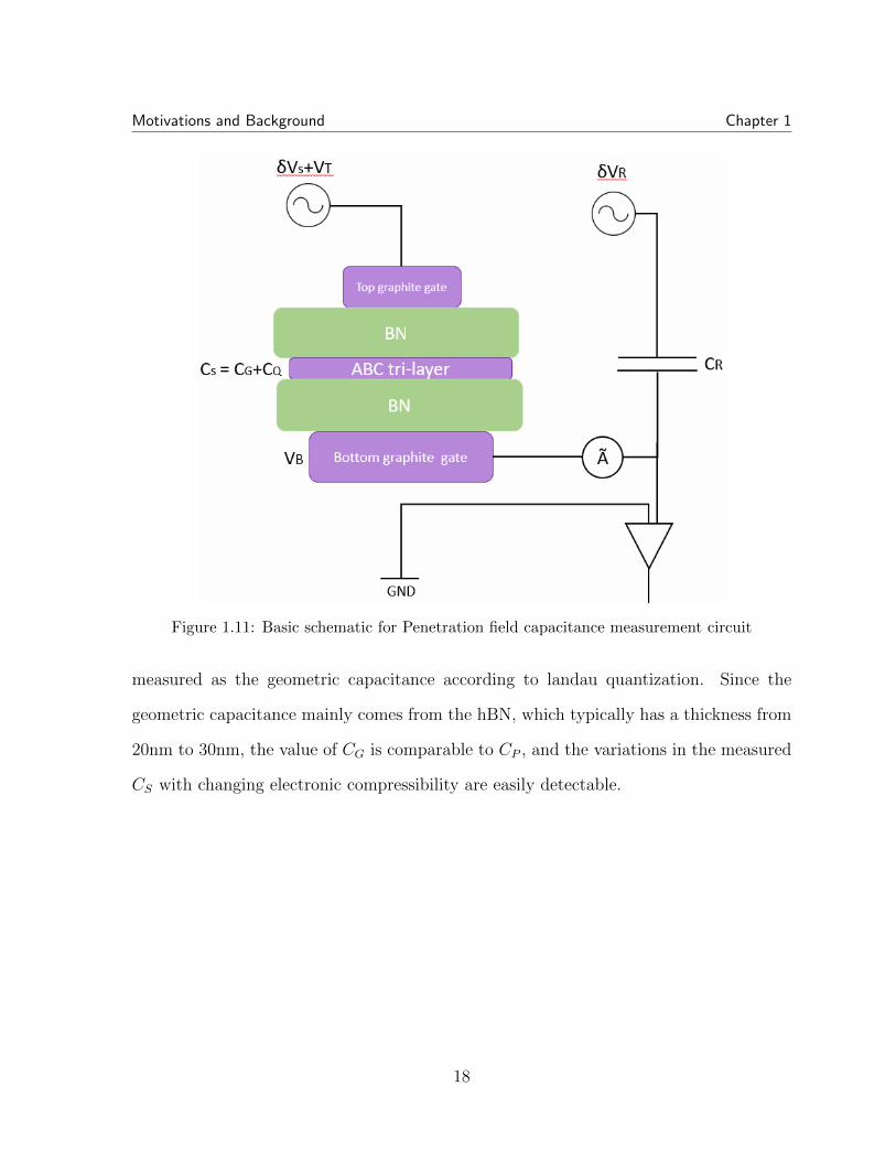
Where CP is called ”Penetration Field Capacitance” which is the quantum capaci-
tance between the top and bottom gate of the Van der Waal hetrostructure . However,
the modulation effect from quantum capacitance is generally much smaller than geomet-
ric capacitance and makes it hard to probe. In 2011, Young et, al. developed a technique
to detect this quantity effectively with the circuit in Fig 1.11 [11].
The main idea is based on a capacitance bridge circuit. We first need to synchronize
the frequency and phase for δVR and δVS. Then balance the amplitude of δVS such that
there are no current flows between CR and CS where CR is the reference capacitance, and
CS is our sample’s capacitance. Then, by comparing the amplitude of δVR and δVS, we
can know the relative ratio between CR and CS. Finally, we can apply a high out-plane
magnetic field, select a relatively low and flat space, and define the average capacitance
17
Motivations and Background Chapter 1
Figure 1.11: Basic schematic for Penetration field capacitance measurement circuit
measured as the geometric capacitance according to landau quantization. Since the
geometric capacitance mainly comes from the hBN, which typically has a thickness from
20nm to 30nm, the value of CG is comparable to CP , and the variations in the measured
CS with changing electronic compressibility are easily detectable.
18
Chapter 2
Fabrication
In past experiments, we know that dual graphite gate devices can significantly suppress
disorder, allowing us to probe fragile phenomena that are absent in metal gated devices.
An example is that in a metal gated device, we can only see integer QH state, but if
we replace both gates with graphite gates, we can then observe fractional QH state up
to a very high order [20]. Therefore, we decide to fabricate dual graphite gates ABC-
trilayer heterostructure. However, there are multiple challenges involved in fabricating
such a device. This chapter will discuss those challenges and provide various effective
techniques that our group has developed for the ABC-trilayer device fabrication.
2.1 Raman Spectroscopy
ABA and ABC phase can appear naturally for trilayer graphene and they have atomic
thickness. Therefore, when they lay on silicon/silicon dioxide substrate, ABA and ABC
will look identical optically since their color is due to interference [13]. So, it is signifi-
cant to differentiate ABA and ABC trilayer graphene. However, since the stacking order
between ABA and ABC trilayer graphene is different, they must have different phonon
19
Fabrication Chapter 2
modes. Thus, a straightforward technique for quantifying this difference is Raman Spec-
troscopy [22].
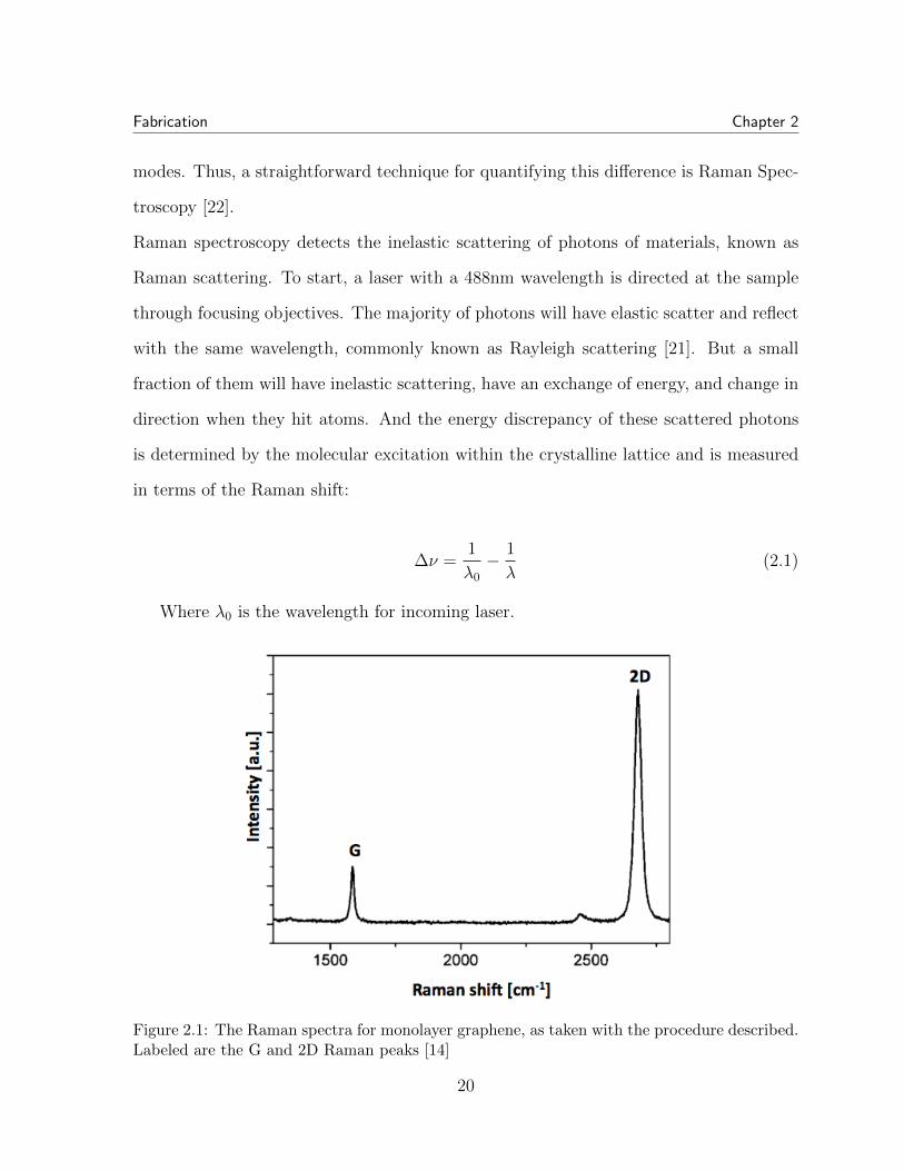
Raman spectroscopy detects the inelastic scattering of photons of materials, known as
Raman scattering. To start, a laser with a 488nm wavelength is directed at the sample
through focusing objectives. The majority of photons will have elastic scatter and reflect
with the same wavelength, commonly known as Rayleigh scattering [21]. But a small
fraction of them will have inelastic scattering, have an exchange of energy, and change in
direction when they hit atoms. And the energy discrepancy of these scattered photons
is determined by the molecular excitation within the crystalline lattice and is measured
in terms of the Raman shift:
∆ν =1
λ0− 1
λ(2.1)
Where λ0 is the wavelength for incoming laser.
Figure 2.1: The Raman spectra for monolayer graphene, as taken with the procedure described.Labeled are the G and 2D Raman peaks [14]
20
Fabrication Chapter 2
Then, the scattered laser, both Raman scattered and Rayleigh scattered light, will
direct through a filter set to the original laser frequency to filter out the Rayleigh scat-
tered (488nm). The remaining Raman scattering light will hit a direction grating, which
separates each component of the beam by the Raman shift in a fan-like pattern. Now
the directed beam hits a CCD that detects counts for each beam. The counts per Ra-
man shift can be plotted, as shown in Fig 2.1, for monolayer graphene. The peaks in
the resulting plots are referred to as Raman peaks, consist of information about lattice
structure and possible phonon modes.
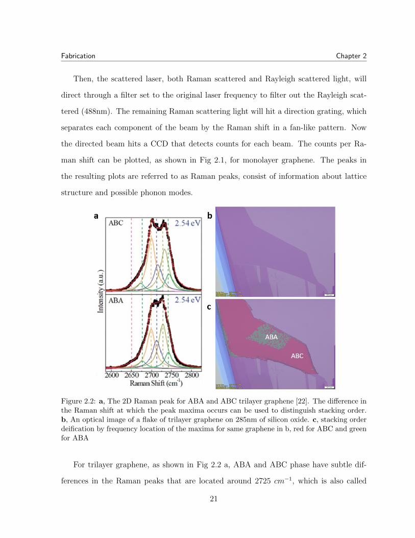
Figure 2.2: a, The 2D Raman peak for ABA and ABC trilayer graphene [22]. The difference inthe Raman shift at which the peak maxima occurs can be used to distinguish stacking order.b, An optical image of a flake of trilayer graphene on 285nm of silicon oxide. c, stacking orderdeification by frequency location of the maxima for same graphene in b, red for ABC and greenfor ABA
For trilayer graphene, as shown in Fig 2.2 a, ABA and ABC phase have subtle dif-
ferences in the Raman peaks that are located around 2725 cm−1, which is also called
21
Fabrication Chapter 2
2D mode in previous works[22, 23, 24]. This peak originates from two optical phonons
close to the K points within the Brillouin zone [25]. Its shape is dependent both on the
stacking order as well as on the excitation energy of the laser. With excitation energy
of 2.54 eV, which corresponds to the 488 nm laser, ABA graphene will have its peak
maximum on the right side of the peak while ABC will be left. From data collected
in other studies [24, 26], this excitation energy and peak pair result most recognizable
difference between ABA and ABC phase.
By taking spectra on each point of our trilayer graphene sample and comparing the fre-
quency shift for the 2D band’s intensity maximum, we can map out the ABA and ABC
domain that previously invisible under the optical microscope, as shown in Fig 2.2.
2.1.1 Procedure
This study is using T64000 Advanced Research Raman System for Raman spec-
troscopy. First, open the water-cooled Coherent INNOVA 300C Argon laser and set it to
the 488nm (2.54eV) line, ramping to a stable operating current of 25A, which associate
with a raw power output of around 300mW. Then the beam will directly go into align-
ment optics and enter the spectrometer.
Then place the sample (in this case, it is trilayer graphene that exfoliated on a diced
low resistivity silicon substrate with 285nm of silicon dioxide top layer) on a motorized
XT stage with microscope above and adjust both the microscope’s focus and stage to
the sample through a 3-axis rotatable joystick. The 488nm beam travels through the
objective, irradiates on the trilayer, then scattered back through the objective and a
488nm Raman filter before entering the spectrometer. An 1800 gr/mm grating is used
for the spectrometer, while the detection range is set between 2470cm−1 and 3020cm−1
to capture the peak located around 2750cm−1.
22
Fabrication Chapter 2
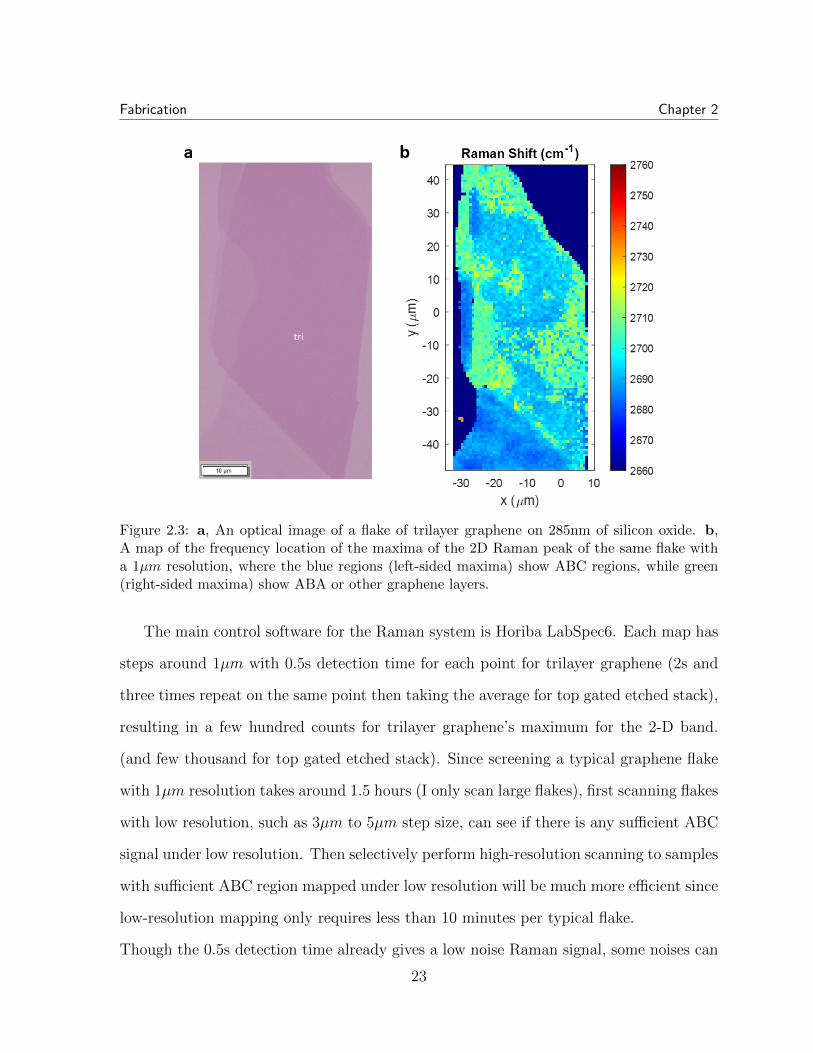
Figure 2.3: a, An optical image of a flake of trilayer graphene on 285nm of silicon oxide. b,A map of the frequency location of the maxima of the 2D Raman peak of the same flake witha 1µm resolution, where the blue regions (left-sided maxima) show ABC regions, while green(right-sided maxima) show ABA or other graphene layers.
The main control software for the Raman system is Horiba LabSpec6. Each map has
steps around 1µm with 0.5s detection time for each point for trilayer graphene (2s and
three times repeat on the same point then taking the average for top gated etched stack),
resulting in a few hundred counts for trilayer graphene’s maximum for the 2-D band.
(and few thousand for top gated etched stack). Since screening a typical graphene flake
with 1µm resolution takes around 1.5 hours (I only scan large flakes), first scanning flakes
with low resolution, such as 3µm to 5µm step size, can see if there is any sufficient ABC
signal under low resolution. Then selectively perform high-resolution scanning to samples
with sufficient ABC region mapped under low resolution will be much more efficient since
low-resolution mapping only requires less than 10 minutes per typical flake.
Though the 0.5s detection time already gives a low noise Raman signal, some noises can
23
Fabrication Chapter 2
still appear at the right side of the 2D-band peak and mislead the mapping. In this
case, using the linear fit to subtract off the background noise, then perform despike and
denoise with level 5 strength in LabSpec6 can improve the data accuracy a lot. It is also
significant to manually check the peak shape for a small ABA island (usually a single
pixel) left in a large ABC domain. In many cases, the peak maximum for “ABA island”
is noise and requires manual removal.
It is also worth noticing that even though the Horiba T64000 can scan with a 500nm
step size, I decide to use 1µm step size for a detailed mapping due to time consumption.
(or else a good trilayer graphene flake full of ABC domain can cost around 6 hours to
scan) Therefore, try to leave more space when avoiding small ABA islands in the ABC
domain during the AFM cutting process, which is the topic for the next section.
2.2 Cutting Graphene with AFM Anodic Oxidation
ABC phase is metastable and can easily relax back to the ABA phase by applying
external energies such as thermal or mechanical agitation. Moreover, compared to the
trilayer graphene flake that only has the ABC phase, the trilayer graphene contain both
ABA and ABC domain is more unstable and tends to dissociate from the ABA phase
due to the energy instability phase boundary [27].
These properties indicate the ABC trilayer graphene could converting back to the ABA
phase during the fabrication process, which is another challenge we need to face. Though
thermal annealing is required for device fabrication and lithography, the temperature
used is much less than the dissociation temperature (over 1000oC) observed in previous
studies [28, 29]. Thus, suppressing mechanical agitation becomes significant to improve
the success rate for fabricating a non-converted ABC heterostructure. In addition, by
isolating the ABC domain in trilayer graphene, the stability of ABC graphene can be
24
Fabrication Chapter 2
enhanced.
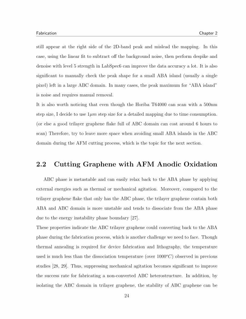
We investigated a previous study [30, 31] in which an AFM tip was used to cut few-layer
graphene using a DC-biased tip with a process known as anodic oxidation. The main
idea is to use voltage applied tip to move across graphene and let the graphene react
with water moisture, electrochemical oxidize to carbon monoxide, and leaving a trench.
By using this way, we can isolate the ABC domain in trilayer graphene.
Figure 2.4: a, flake of exfoliated trilayer graphene. b, The intended grid to be cut. c, The flakeafter the AFM AC anodic oxidation cutting technique.
This technique has adapted to our AFM, a Bruker Dimension Icon. However, applying
DC voltage [30] to a electrically floated graphite could accumulate a large charge on the
flake, obstruct further AFM imaging. Thus, we used 100kHz frequency, 10V amplitude
AC voltage to Bruker SCM-PITV2 (or ArrowNCPt tip) metalized tip to perform a slow
cutting (50nm/s) to make a more reliable cut and exclude charge buildup.
25
Fabrication Chapter 2
2.3 Polypropylene carbonate Dry Transfer Process
The devices in this project were mainly fabricated with the standard Polypropylene
carbonate (PPC) dry transfer process. Therefore, first is the procedure to create a PPC
pickup slide.
A 4mm cylinder of polydimethylsiloxane (PDMS) with a 3mm diameter is placed on
a standard microscope slide and then covered with transparent tape to create a dome.
Typically, we use 2mm diameter PDMS, but to reduce the mechanical agitation applied
to ABC, we use PDMS with a larger diameter to reduce the dome’s curve. Spin coat a
few drops of 9% polypropylene carbonate (PPC)/anisole solution on a silicon substrate
with 4000 spins/min for 1min. Then, anneal the spin-coated wafer at 90oC for 2 min
and 30 seconds. The film is then transferred to the dome on pickup slide by a one-sided
tape with hole at the center. If there are bubbles present, anneal slide at 90oC for an
additional 1 min. If the bubble does not disappear, raise the annealing temperature to
10oC and repeat the annealing process until the temperature reaches 130oC. Usually, it
will resolve most of the bubble.
Then is the procedure for the transfer process. First, placed the silicon wafer that has
the exfoliated flake for picked up on a transfer station’s vacuum holder with a PID-
controlled heater and microscope on top of them. Then open the vacuum and set the
PID temperature to 40oC for pickup flakes. Next, lower the pickup slide by a Z-positioner
until the newton ring appears on the surface of the chip to locate the touchdown point.
Then move the pickup slide by X and Y-positioner until the touchdown point gets close
to the flake. Then use Z-positioner to adjust the pickup slide’s Z position until PPC
covered the needed flake and raise the stage back to pick up hBN and graphite.
Since PDMS has a high coefficient of thermal expansion, the adjusted temperature can
also use to change Z-position for PPC. So, a more controllable but less efficient way to
26
Fabrication Chapter 2
pick up a flake is through temperature control. After correctly adjust the XZY position
for the pickup slide and there is already a small area of PPC contact with the substrate,
raise the temperate for PID-heater by 0.5oC or 1oC step, then wait for 5min. Repeat the
cycle until PPC covered the needed flake. Then lower the temperature back by 1oC step
and wait about 7min to allow the stage to cool passively. Repeat cycle until complete
pickup. During the lifting process, pay attention to PPC/silicon wafer boundary and
adjust Z-positioner to avoid PPC from spontaneously ‘jumping.’ After picking up a
flake, re-anneal the pickup slide by 90oC, 1min to re-flatten the small PPC corrugations
create during the pickup process.
PPC has difficulty picking up graphite and graphene flake as the first layer. Thus, we
need first to pick up an hBN flake first for further fabrication. The completed stack is then
released from the pickup slide onto a piece of silicon with alignment marks by lowering
the Z-positioner and increasing the temperature over 140oC to melt the PPC film. Then
the transferred stack can be cleaned by withering acetone/IPA bath or annealing around
375oC.
2.3.1 Squeeze Bubble
There are possibilities for air, water moisture, and other polymers to be encapsulated
in the heterostructure during the fabrication process and create some bumps. We usually
call them bubbles. The bubbles encapsulated in the heterostructure will cause inhomo-
geneity of device geometry, leading to disorder and prohibit the measurement of fragile
physical phenomena. Thus, it is essential to create a bubble-free sample. However, the
formation of bubbles is almost unavoidable. So, we generally will try to clean the bubble
in the heterostructure by what we call squeezing bubble. We first raise the temperature
for PID-heater to 90oC to increase the bubble’s mobility since they are mainly gas and
27
Fabrication Chapter 2
liquid. Then adjust the relative angle between pickup slide and vacuum holder to 2o to 3o
and place a clean, unused silicon substrate to the holder. Next, lowering the pickup slide
with finished or partially finished heterostructure to the silicon wafer by the Z-positioner.
Finally, adjust the Z position until the boundary between PPC and silicon substrate is
on the heterostructure. Since there is a sharp angle between the heterostructure on the
wafer and the PPC film at the boundary, we can move the boundary back and forth by
adjusting Z-positioner to squeeze the bubbles out.
2.3.2 PPC Flipping Technic and Rapid Thermal Annealing
To further avoid the mechanical agitation for ABC trilayer graphene. We decide to
decompose the device into two parts: the top and bottom parts, where the last layer for
the top part is ABC trilayer graphene. Then, assemble the top part with the pre-made
bottom part to finish the desired stack. In this way, ABC trilayer graphene will only get
pick up and put down once, which minimizes the mechanical agitation applied to ABC
trilayer graphene. However, the top surface ABC graphene will contact the pre-made
bottom part of the stack, polluted by either acetone/IPA bath or thermal annealing.
There will always be some polymer leftover on the top surface for the pre-made bottom
part. Thus, we decide to flip the bottom part such that ABC graphene will contact
the bottom part of the bottom stack, which is an untouched surface through the whole
transfer process. The theoretical process is relatively simple. Once using PPC film to
pick up the bottom hBN/graphite/hBN part, take off the PPC film. Then flipping the
PPC film to a substrate and bake the substrate at 375oC by rapid thermal annealing to
melt the PPC film. However, in actual practice, this flipping technique requires some
other constraints during fabrication. For example, during the process of taking off PPC
film, there is a good possibility for the PPC film to partially stick on the transparent tape
28
Fabrication Chapter 2
and leave cracks on the stack. Therefore, during the fabrication of PPC pickup slides
and pick up process, the annealing temperate needs to lower or equal to 90oC to avoid
potential sticking.
2.3.3 Aligning Crystalline Lattices
As discussed in Chapter 1, to observe strongly correlated physics phenomena through
a flat band, we need to align the crystal axis of ABC trilayer graphene and hBN with a
small-angle difference to create proper moire superlattice. Or at least one of the trilayer-
encapsulating hBN flakes must have its crystalline lattice aligned with the trilayer. We
attempt to align the crystalline lattice of hBN with the trilayer for each stack by aligning
their natural straight edge. We identify the straight edge of the flake if two straight edges
have a relative angle equal to the multiple of 30oC. However, even if having perfect angle
control, there is still only a 50% chance of hBN-trilayer alignment for each side due to
the two naturally occurring lattice edges of a hexagonal lattice.
2.4 ABC-Trilayer Stacking Procedure and Extra Tips
Though a device with a large area provides more accurate and quicker capacitance
measurement, a large device has a higher possibility of obtaining ABA islands in the
ABC region inside the device, which can not be detected during the re-Raman process.
Therefore, cutting ABC graphene to size around 40µm2 to 100µm2 (8x5 to 10x10) will
be the most convenient size for a device.
Moreover, since ABC trilayer graphene has the possibility to relax back to ABA during
fabrication, using a large ABC graphene that is cutted to three to four pieces in a row
can increase the overall success rate to fabricate an unconverted sample.
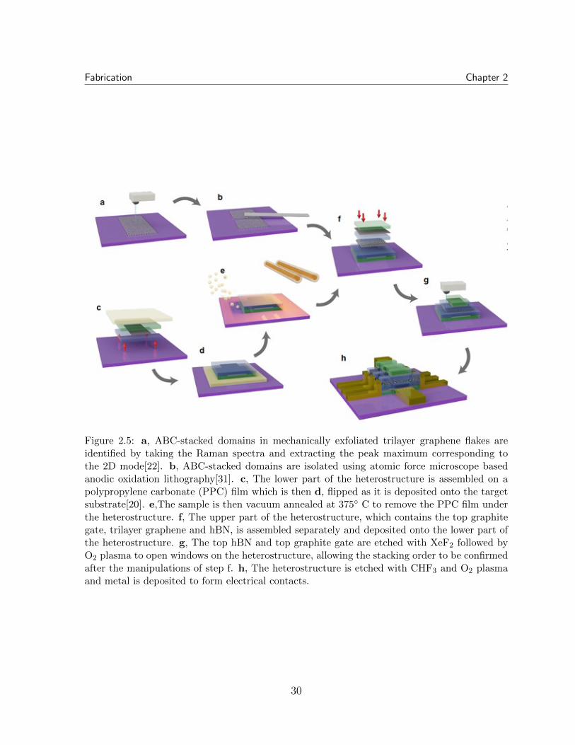
Our optimized trilayer stacking process are shown in Fig 2.5:
29
Fabrication Chapter 2
Figure 2.5: a, ABC-stacked domains in mechanically exfoliated trilayer graphene flakes areidentified by taking the Raman spectra and extracting the peak maximum corresponding tothe 2D mode[22]. b, ABC-stacked domains are isolated using atomic force microscope basedanodic oxidation lithography[31]. c, The lower part of the heterostructure is assembled on apolypropylene carbonate (PPC) film which is then d, flipped as it is deposited onto the targetsubstrate[20]. e,The sample is then vacuum annealed at 375 C to remove the PPC film underthe heterostructure. f, The upper part of the heterostructure, which contains the top graphitegate, trilayer graphene and hBN, is assembled separately and deposited onto the lower part ofthe heterostructure. g, The top hBN and top graphite gate are etched with XeF2 followed byO2 plasma to open windows on the heterostructure, allowing the stacking order to be confirmedafter the manipulations of step f. h, The heterostructure is etched with CHF3 and O2 plasmaand metal is deposited to form electrical contacts.
30
Chapter 3
Device Measurements and Outlook
All measurement data shown in this chapter for our devices (BX-st10-TM and HZS220)
was taken in the Bluefors dilution refrigerator, and Bluefors vector filed dilution refrig-
erator at a base temperature of 10 mK.
Even though in the previous chapters, it is believed that having hBN/ABC superlattice
is significant to observe novel physics phenomenon, we’ve also observed many interesting
physical phenomena in pure ABC trilayer sample, which can help us to understand the
phenomenon observed in superlattice sample. Thus, I will start with data of unaligned
ABC device.
3.1 Data for unaligned sample (HZS220)
Instead of transport measurement, let’s discuss the capacitance data, which has a
much simpler physical meaning.
We first only tuning the charge carrier density (n0) for the ABC. The most obverse
structure is the peak at charge neutral point (CNP), which implies a low density of state
(DOS). This peak can be explained by ABC’s energy band while not considering Coulomb
31
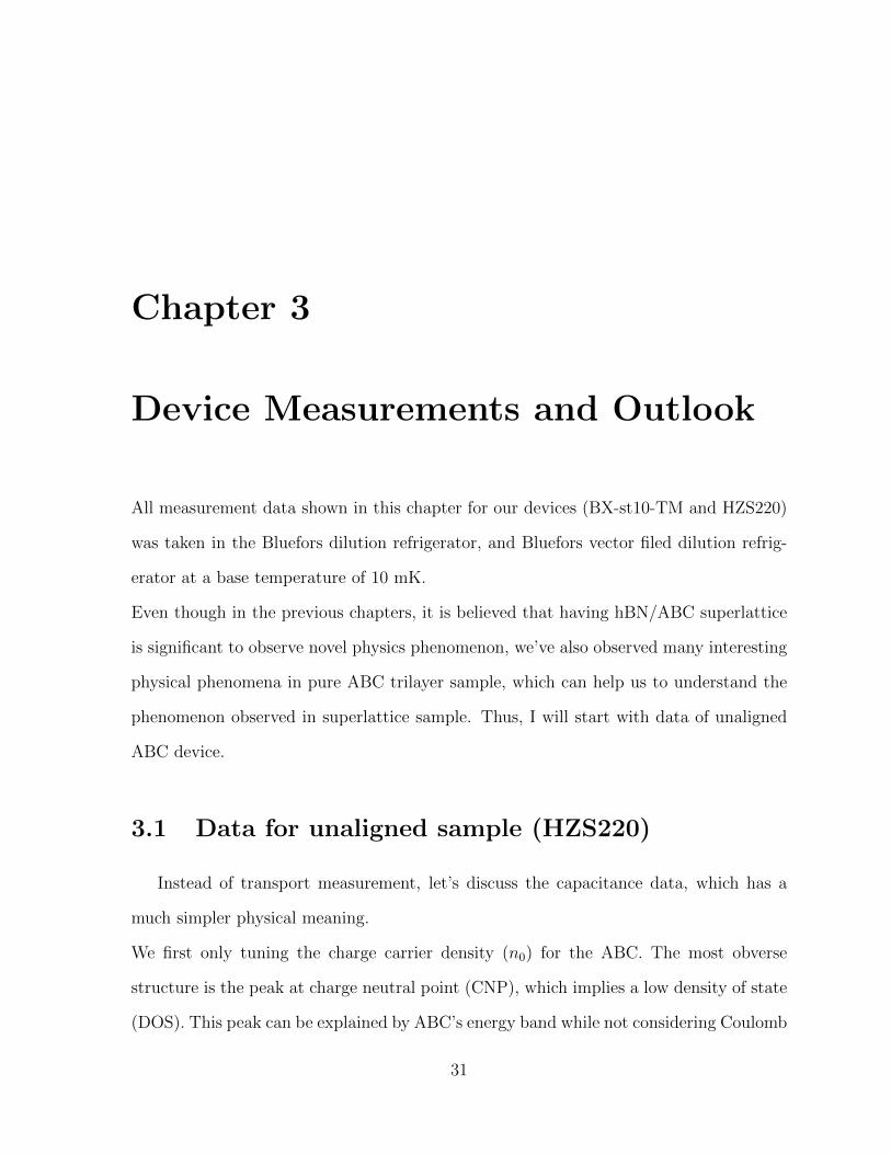
Device Measurements and Outlook Chapter 3
interaction. When zooming in to the low incompressibility region of the graph, two rapid
changes of density of state can be observed. The main features in the line plot can be
reproduced purely by using the single electron model for ABC mentioned in chapter 1. If
we related the line plot to the cross-section of the energy band for ABC, we could see the
steps in Fig 3.1 a are caused by Lifshitz transitions, where the Fermi surface changes its
topology. For example, the step at left is caused by Lifshitz transitions where the Fermi
surface changes from a disk to an annulus.
Figure 3.1: a, Black: inverse compressibility as a function of carrier density measured atzero displacement field. Blue: reverse of the DOS calculated from the six-band continuummodel.Insets: Fermi contours calculated from the continuum model. The wave vectors rangesfrom −0.05κ · a0 to 0.05κ · a0 in both x- and y- axes for each plot. b, The 3D energy band forABC trilayer graphene with energy cross sections corresponding to the Fermi contours in a.
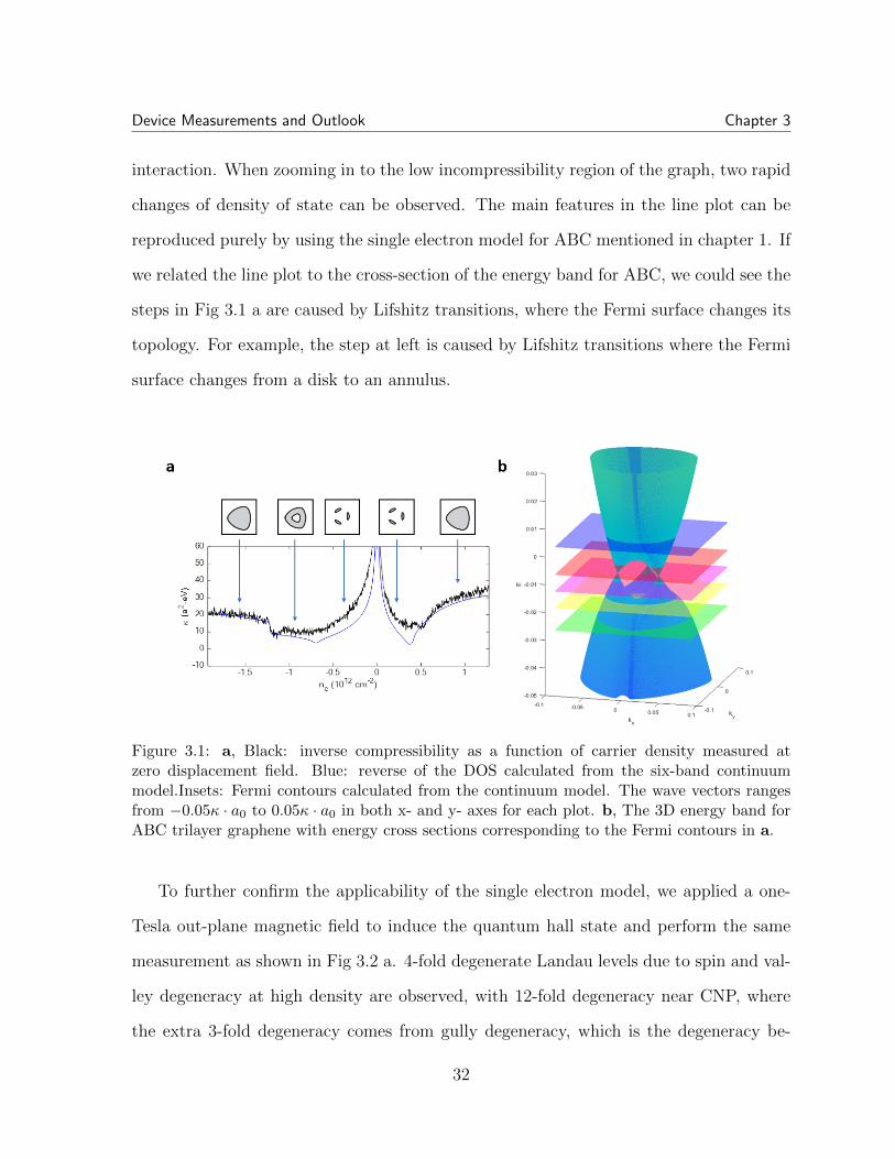
To further confirm the applicability of the single electron model, we applied a one-
Tesla out-plane magnetic field to induce the quantum hall state and perform the same
measurement as shown in Fig 3.2 a. 4-fold degenerate Landau levels due to spin and val-
ley degeneracy at high density are observed, with 12-fold degeneracy near CNP, where
the extra 3-fold degeneracy comes from gully degeneracy, which is the degeneracy be-
32
Device Measurements and Outlook Chapter 3
tween the three pockets in the band structure. This effect was also observed in ABA
trilayer graphene [32]. Notice the peak at the charge neutral point is not caused by the
quantum hall effect. As shown in the Fig 3.2 b, the peak at charge neutral point appears
after the magnetic field applied over 0.1 Tesla. Thus, that peak is caused by other effects
other than the single electron quantum hall effect.
Figure 3.2: a, inverse compressibility as a function of carrier density measured at one Teslaperpendicular magnetic field. b, inverse compressibility as a function of carrier density measuredand perpendicular magnetic field.
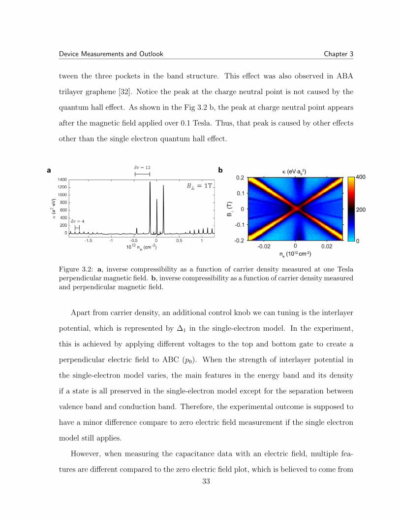
Apart from carrier density, an additional control knob we can tuning is the interlayer
potential, which is represented by ∆1 in the single-electron model. In the experiment,
this is achieved by applying different voltages to the top and bottom gate to create a
perpendicular electric field to ABC (p0). When the strength of interlayer potential in
the single-electron model varies, the main features in the energy band and its density
if a state is all preserved in the single-electron model except for the separation between
valence band and conduction band. Therefore, the experimental outcome is supposed to
have a minor difference compare to zero electric field measurement if the single electron
model still applies.
However, when measuring the capacitance data with an electric field, multiple fea-
tures are different compared to the zero electric field plot, which is believed to come from
33
Device Measurements and Outlook Chapter 3
Figure 3.3: a, The 3D energy band for ABC trilayer graphene at zero displacement field. b,inverse compressibility as a function of carrier density measured at zero displacement field. c,The 3D energy band for ABC trilayer graphene at -0.31V/nm displacement field. d, inversecompressibility as a function of carrier -0.31V/nm displacement field. e, theoretical simulationof inverse compressibility as a function of carrier density and displacement field by single electronmodel. f, measured inverse compressibility as a function of carrier density and displacementfield with cross line at D=0V/nm (blue) and D=-0.31V/nm (green).
Coulomb interaction. We actually measured the complete electric field vs. charge car-
rier density vs. inverse compressibility graph. We observed multiple dips with negative
inverse compressibility when applying an electric field, indicating 1st order phase transi-
tions. Suppose we use the single-electron model to calculate the inverse compressibility
graph in the same 2-D range. In that case, we can see that it only predicts the features
with 4-fold degeneracy and the peak at CNP. Therefore, we believe the rest features are
coming from electron-electron interaction.
To understand the nature of these multiple emerged phases, we performed the same
measurement with a one-Tesla out-plane magnetic field (Fig 3.4 a). The multiple vertical
34
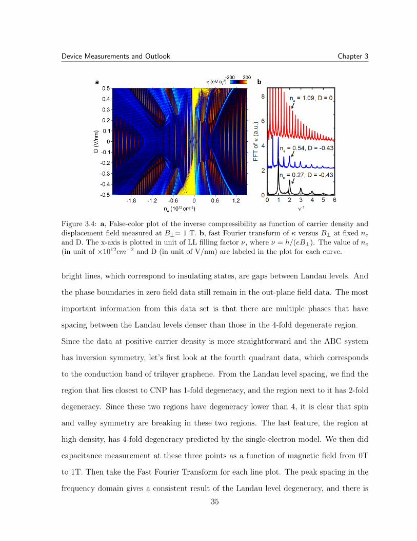
Device Measurements and Outlook Chapter 3
Figure 3.4: a, False-color plot of the inverse compressibility as function of carrier density anddisplacement field measured at B⊥= 1 T. b, fast Fourier transform of κ versus B⊥ at fixed neand D. The x-axis is plotted in unit of LL filling factor ν, where ν = h/(eB⊥). The value of ne(in unit of ×1012cm−2 and D (in unit of V/nm) are labeled in the plot for each curve.
bright lines, which correspond to insulating states, are gaps between Landau levels. And
the phase boundaries in zero field data still remain in the out-plane field data. The most
important information from this data set is that there are multiple phases that have
spacing between the Landau levels denser than those in the 4-fold degenerate region.
Since the data at positive carrier density is more straightforward and the ABC system
has inversion symmetry, let’s first look at the fourth quadrant data, which corresponds
to the conduction band of trilayer graphene. From the Landau level spacing, we find the
region that lies closest to CNP has 1-fold degeneracy, and the region next to it has 2-fold
degeneracy. Since these two regions have degeneracy lower than 4, it is clear that spin
and valley symmetry are breaking in these two regions. The last feature, the region at
high density, has 4-fold degeneracy predicted by the single-electron model. We then did
capacitance measurement at these three points as a function of magnetic field from 0T
to 1T. Then take the Fast Fourier Transform for each line plot. The peak spacing in the
frequency domain gives a consistent result of the Landau level degeneracy, and there is
35
Device Measurements and Outlook Chapter 3
no recovery of the degeneracy as the field decreases. This result indicates the observed
degeneracy in different regions is not induced by the magnetic field; they are rather
intrinsic properties of the rhombohedral trilayer graphene. To further understand the
degeneracy region in ABC, we’ve then collaborated with Serbyn‘s group in IST Austria
and use the stoner model to simulate our measured plot.
3.2 Simulation for unaligned sample (HZS220)
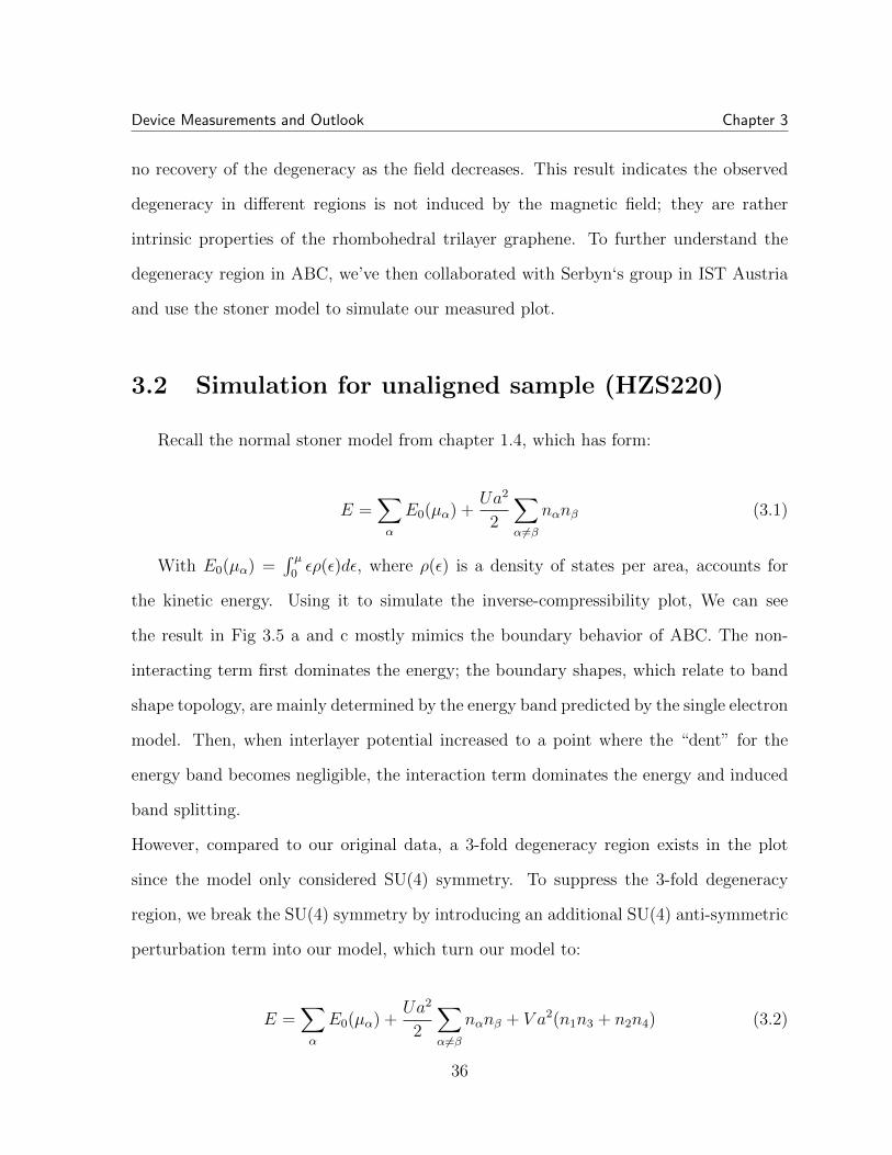
Recall the normal stoner model from chapter 1.4, which has form:
E =∑α
E0(µα) +Ua2
2
∑α 6=β
nαnβ (3.1)
With E0(µα) =∫ µ0ερ(ε)dε, where ρ(ε) is a density of states per area, accounts for
the kinetic energy. Using it to simulate the inverse-compressibility plot, We can see
the result in Fig 3.5 a and c mostly mimics the boundary behavior of ABC. The non-
interacting term first dominates the energy; the boundary shapes, which relate to band
shape topology, are mainly determined by the energy band predicted by the single electron
model. Then, when interlayer potential increased to a point where the “dent” for the
energy band becomes negligible, the interaction term dominates the energy and induced
band splitting.
However, compared to our original data, a 3-fold degeneracy region exists in the plot
since the model only considered SU(4) symmetry. To suppress the 3-fold degeneracy
region, we break the SU(4) symmetry by introducing an additional SU(4) anti-symmetric
perturbation term into our model, which turn our model to:
E =∑α
E0(µα) +Ua2
2
∑α 6=β
nαnβ + V a2(n1n3 + n2n4) (3.2)
36
Device Measurements and Outlook Chapter 3
We consider the energy is lowest at a spin polarize, valley unpolarized phase. Though
the interaction constant for the SU(4) anti-symmetric term is very large as a pertur-
bation term, but the simulated result almost perfectly restored all the features in the
measured data. To confirm the spin and valley flavor for each phase, we measured the
incompressibility under a parallel magnetic field (Fig 3.5 f). The straight boundary line
between 1 and 2-fold region shows that the 2-fold degeneracy region is a spin polarized
region since the 1-fold region must be spin and valley polarized, which also confirmed
that our model did the correct speculation. Or else the boundary line will be curved like
the one at the high-density region where the 4-fold region is indeed spin unpolarized. We
now can relate our Fermi contours with the phase in each region (Fig 3.5 d and e).
Figure 3.5: a, Partial densities of each spin-valley flavor as a function of the total densitycalculated from the Stoner model at a fixed interlayer potential of 20meV and U=30 eV, V=0.b, Same results with U=30eV, V=-10eV. c, Inverse compressibility at ne >0, B=0 calculatedfrom the Stoner model with U=30eV, V=-10eV. Inset: Same results with U=30 eV, V=0. d,False-color plot of the inverse compressibility as function of carrier density and displacementfield with their degeneracy labeled on each region. e, Fermi contours of each flavor correspondingto the three carrier density values indicated by the arrows in d. The Fermi contours are filledwith different colors to distinguish the spin- and valley- flavors. f, In-plane magnetic fielddependence of the inverse compressibility measured at D = -0.43 V/nm [34].
37
Device Measurements and Outlook Chapter 3
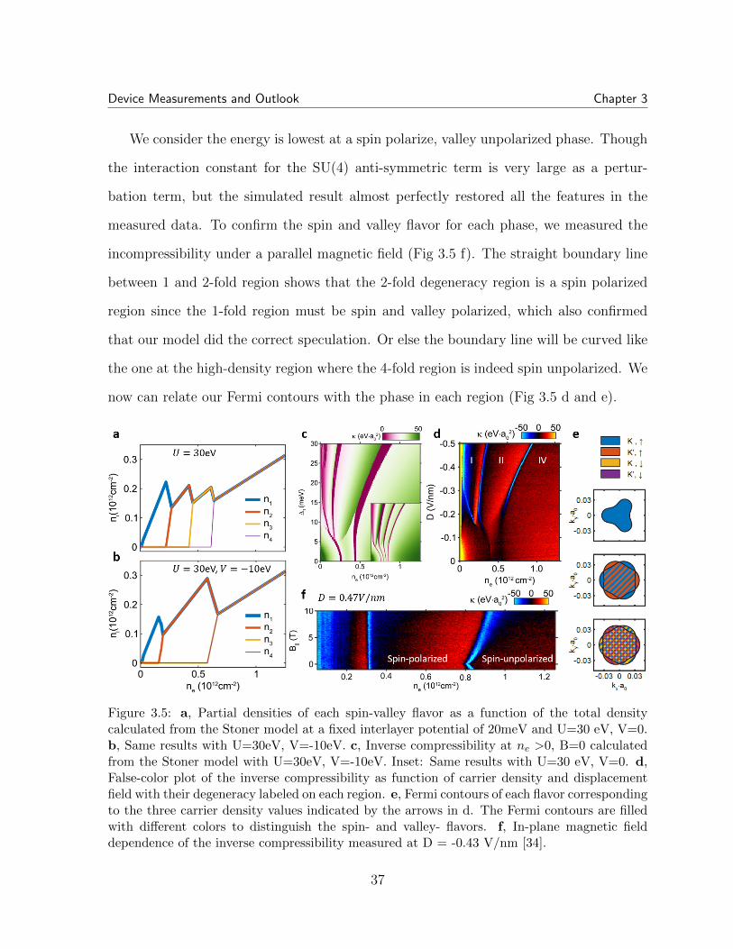
Now, let’s discuss the side with more complex behavior, the valance band. By the
same inversion symmetry argument, we will only look at the data in the second quadrant.
In the zero-field data (Fig 3.6 a), the hole side has many more regions compare to the
electron side (Fig 3.6 c). However, through the 1 Tesla out-plane magnetic field data
(Fig 3.6 b), we find the degeneracy between II and III, IV and V, VI and VII are all the
same, and their phase boundary is just caused by Lifshitz transition (Fig 3.6 d). Thus,
even though the topology of Fermi contour changes and leads to the weird landau level
crossing in region II, IV, and V, the flavor of the between these phase pair are still the
same. And by repeating similar stoner model simulation, we can again relate our Fermi
contours with the phase in each region.
Figure 3.6: a, False-color plot of the inverse compressibility versus carrier density and dis-placement field. b, Same results with 1 Tesla out-plane magnetic field. c, Schematic phasediagram extracted from a. d, Schematic Fermi contours of each phase defined in c. Filledcolors represent the spin- and valley- flavors, following the same convention in Fig. 3.5 e [34].
38
Device Measurements and Outlook Chapter 3
As we got some understanding for the ABC trilayer graphene without moire supper
lattice, let’s now go back to this project’s original purpose, detecting Coulomb interaction
in ABC trilayer graphene with moire superlattice.
3.3 Data for aligned sample (BX-ST10-TM)
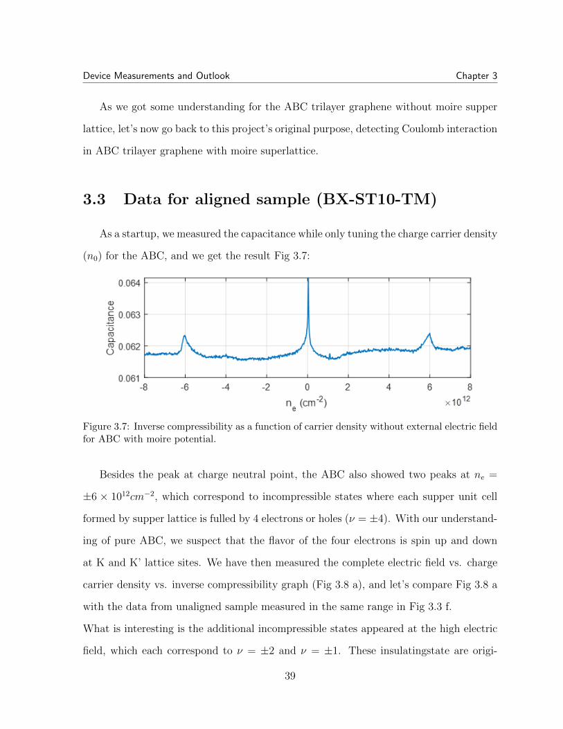
As a startup, we measured the capacitance while only tuning the charge carrier density
(n0) for the ABC, and we get the result Fig 3.7:
Figure 3.7: Inverse compressibility as a function of carrier density without external electric fieldfor ABC with moire potential.
Besides the peak at charge neutral point, the ABC also showed two peaks at ne =
±6 × 1012cm−2, which correspond to incompressible states where each supper unit cell
formed by supper lattice is fulled by 4 electrons or holes (ν = ±4). With our understand-
ing of pure ABC, we suspect that the flavor of the four electrons is spin up and down
at K and K’ lattice sites. We have then measured the complete electric field vs. charge
carrier density vs. inverse compressibility graph (Fig 3.8 a), and let’s compare Fig 3.8 a
with the data from unaligned sample measured in the same range in Fig 3.3 f.
What is interesting is the additional incompressible states appeared at the high electric
field, which each correspond to ν = ±2 and ν = ±1. These insulatingstate are origi-
39
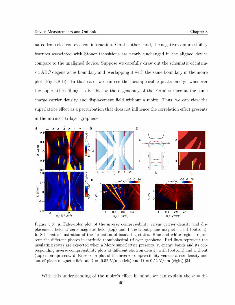
Device Measurements and Outlook Chapter 3
nated from electron-electron interaction. On the other hand, the negative compressibility
features associated with Stoner transitions are nearly unchanged in the aligned device
compare to the unaligned device. Suppose we carefully draw out the schematic of intrin-
sic ABC degeneracies boundary and overlapping it with the same boundary in the moire
plot (Fig 3.8 b). In that case, we can see the incompressible peaks emerge whenever
the superlattice filling is divisible by the degeneracy of the Fermi surface at the same
charge carrier density and displacement field without a moire. Thus, we can view the
superlattice effect as a perturbation that does not influence the correlation effect presents
in the intrinsic trilayer graphene.
Figure 3.8: a, False-color plot of the inverse compressibility versus carrier density and dis-placement field at zero magnetic field (top) and 1 Tesla out-plane magnetic field (bottom).b, Schematic illustration of the formation of insulating states. Blue and white regions repre-sent the different phases in intrinsic rhombohedral trilayer graphene. Red lines represent theinsulating states are expected when a Moire superlattice presents. c, energy bands and its cor-responding inverse compressibility plots at different electron density with (bottom) and without(top) moire present. d, False-color plot of the inverse compressibility versus carrier density andout-of-plane magnetic field at D = -0.52 V/nm (left) and D = 0.52 V/nm (right) [34].
With this understanding of the moire’s effect in mind, we can explain the ν = ±2
40
Device Measurements and Outlook Chapter 3
and ν = ±1 insulating states by the band plot (Fig 3.8 c) where we consider the energy
band structure is a function associated with charge carrier density.
In the unaligned case, the valence band split into two levels when electron density and
displacement field are in the 2-fold degenerate region. Then consider superlattice as an
additional superposition effect to the band, where it only split the bands and leads to
simple two-level systems, which result in the Mott insulating state.
Other than describing the gapped states using electron per superlattice site “s”, another
good quantum number for us to describe the ABC system is the Chern number “t”, which
linked to the quantized Hall conductivity. We classify gaps by the resulting trajectories
in the n-B⊥ plane using equation:
ν = tnφ + s (3.3)
Where nφ is the number of magnetic flux quanta per unit cell. We measured the
incompressibility v.s n and B⊥ 2-D data at fix displacement field (Fig. 3.8 d) at each
insulating states. Consistent with prior work, we find that commensurate insulators at
ν = −1 and ν = −2 states are topologically trivial for D>0, but in contrast, the ν = −1
insulator is nontrivial for D<0. To find the Chern number, We then observe a close
competition between t=-2 and t=-3 slope for the Chern insulating sate. As B⊥ tends to
go to zero and the states converge to the same density, the more robust t=-2 state wins
the energetic competition.
3.4 Additional data
We not only measured many physics phenomena that have been well modeled from
ABC trilayer graphene but there are also many phenomena that we have not fully un-
41
Device Measurements and Outlook Chapter 3
derstand. This section will present some of the unknown features we observed in both
aligned and unaligned ABC trilayer samples.
3.4.1 ABC with moire
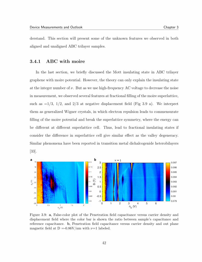
In the last section, we briefly discussed the Mott insulating state in ABC trilayer
graphene with moire potential. However, the theory can only explain the insulating state
at the integer number of ν. But as we use high-frequency AC voltage to decrease the noise
in measurement, we observed several features at fractional filling of the moire superlattice,
such as =1/3, 1/2, and 2/3 at negative displacement field (Fig 3.9 a). We interpret
them as generalized Wigner crystals, in which electron repulsion leads to commensurate
filling of the moire potential and break the superlattice symmetry, where the energy can
be different at different superlattice cell. Thus, lead to fractional insulating states if
consider the difference in superlattice cell give similar effect as the valley degeneracy.
Similar phenomena have been reported in transition metal dichalcogenide heterobilayers
[33].
Figure 3.9: a, False-color plot of the Penetration field capacitance versus carrier density anddisplacement field where the color bar is shown the ratio between sample’s capacitance andreference capacitance. b, Penetration field capacitance versus carrier density and out planemagnetic field at D =-0.86V/nm with ν=1 labeled.
42
Device Measurements and Outlook Chapter 3
On the other hand, even though ν=1 insulating state is topologically trivial, we can
still observe interesting feature when we focus on the low B regime and measure the n0
v.s B⊥ v.s incompressibility data at a fix displacement field as shown in Fig 3.9 b.
The incompressibility for the ν=1 insulating state first decreases as the perpendicular
magnetic field increases up to a critical magnetic field around 0.4T; then it starts to grow
along the field, which indicates a phase transition along the magnetic field. Moreover,
the fractional filling insulating state also behaves similarly to the ν=1 insulating state.
This behavior is anomalous compare to a normal integer filling insulting state.
3.4.2 ABC without morie
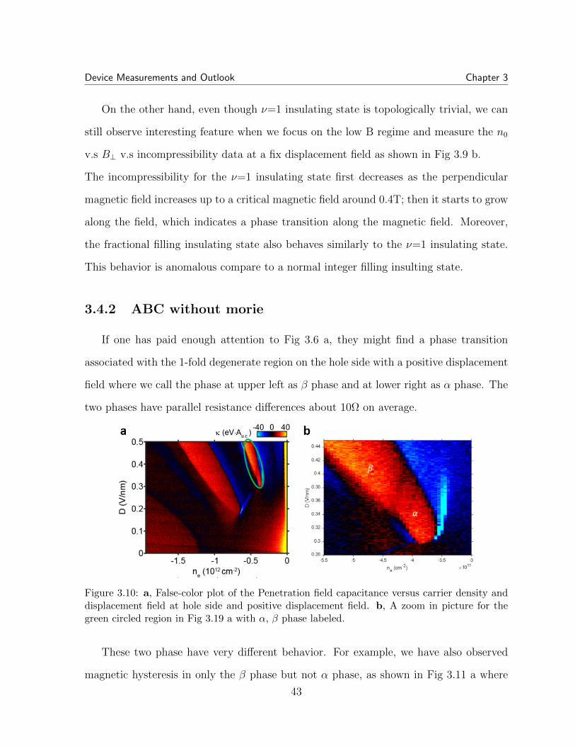
If one has paid enough attention to Fig 3.6 a, they might find a phase transition
associated with the 1-fold degenerate region on the hole side with a positive displacement
field where we call the phase at upper left as β phase and at lower right as α phase. The
two phases have parallel resistance differences about 10Ω on average.
Figure 3.10: a, False-color plot of the Penetration field capacitance versus carrier density anddisplacement field at hole side and positive displacement field. b, A zoom in picture for thegreen circled region in Fig 3.19 a with α, β phase labeled.
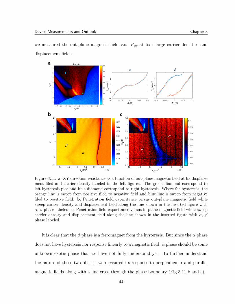
These two phase have very different behavior. For example, we have also observed
magnetic hysteresis in only the β phase but not α phase, as shown in Fig 3.11 a where
43
Device Measurements and Outlook Chapter 3
we measured the out-plane magnetic field v.s. Rxy at fix charge carrier densities and
displacement fields.
Figure 3.11: a, XY direction resistance as a function of out-plane magnetic field at fix displace-ment filed and carrier density labeled in the left figures. The green diamond correspond toleft hysteresis plot and blue diamond correspond to right hysteresis. Where for hysteresis, theorange line is sweep from positive filed to negative field and blue line is sweep from negativefiled to positive field. b, Penetration field capacitance versus out-plane magnetic field whilesweep carrier density and displacement field along the line shown in the inserted figure withα, β phase labeled. c, Penetration field capacitance versus in-plane magnetic field while sweepcarrier density and displacement field along the line shown in the inserted figure with α, βphase labeled.
It is clear that the β phase is a ferromagnet from the hysteresis. But since the α phase
does not have hysteresis nor response linearly to a magnetic field, α phase should be some
unknown exotic phase that we have not fully understand yet. To further understand
the nature of these two phases, we measured its response to perpendicular and parallel
magnetic fields along with a line cross through the phase boundary (Fig 3.11 b and c).
44
The phase boundary for the perpendicular magnetic field has close linear behavior, and
the parallel magnetic field has close quadratic behavior. In addition that the system
starts to show quantum fluctuation in the high perpendicular magnetic field region; we
suspect the difference between two phases is from their valley polarization.
3.5 Concluding Thoughts
In this project, we have successfully fabricated and measured both aligned and not
aligned ABC devices while setup a standard operation process to fabricate rhombohedral
trilayer graphene devices. On the other hand, we have not only measured and confirmed
multiple features that have been reported by other groups, such as correlated insulating
states in aligned ABC devices, but we have also revealed some novel phases in intrin-
sic ABC trilayer graphene such as ferromagnetism and established simple and effective
model to mimic electron behavior in both aligned and not aligned ABC system.
Compare to well-known quantum hall ferromagnetism, the ferromagnetism reveal in the
rhombohedral trilayer graphene system is spin and valley ferromagnetism. Unlike other
ferromagnet systems, the ferromagnets in trilayer graphene are metallic and do not re-
quire an external magnetic field like quantum hall ferromagnetism. Moreover, the ferro-
magnetism does not originate from tightly localized atomic orbitals like other itinerant
ferromagnets, such as transition metals. In this respect, rhombohedral trilayer graphene
is an “intrinsic” itinerant isospin ferromagnet, taking both advantage of quantum Hall
ferromagnets and more conventional magnetic metals. Therefore, provide a good plat-
form to study ferromagnetism. Similar ferromagnetic states have also been shown in
multilayer graphene systems [9]. Thus, it will be interesting to further study multilayer
rhombohedral graphene systems such as ABCA or ABCAB and explore the relationship
between the graphene layer and their shared properties.
45
Bibliography
[1] Chen, G. et al. Signatures of Gate-Tunable Superconductivity in TrilayerGraphene/Boron Nitride Moire Superlattice. Nature. 557, 215–219. (Jul. 2019).
[2] Novoselov, K. et al. Electric Field Effect in Atomically Thin Carbon Films. Science.306, 666-669. (Oct. 2004).
[3] Zhang, Y. et al. Experimental observation of the quantum Hall effect and Berry’sphase in graphene. Nature. 438, 201–204. (Nov. 2005).
[4] Dean, C. R. et al. Boron nitride substrates for high-quality graphene electronics.Nature Nanotechnology. 5, 722–726. (Aug. 2010).
[5] Zomer, P. J. et al. Fast pick up technique for high quality heterostructures of bilayergraphene and hexagonal boron nitride. arXiv: 1403.0399 [cond-mat]. (Mar. 2014).
[6] Zibrov, A. A. et al. Tunable interacting composite fermion phases in a half-filledbilayer-graphene Landau level. Nature. 549, 360–364. (Sep. 2017).
[7] Cao, Y. et al. Unconventional Superconductivity in Magic-Angle Graphene Superlat-tices. Nature. 556, 43-50. (Apr. 2018).
[8] Lee, Y. et al. Gate Tunable Magnetism and Giant Magnetoresistance in ABC-stackedFew-Layer Graphene. arXiv: 1911.04450 [cond-mat]. (Nov. 2019).
[9] Shi, Y. et al. Electronic phase separation in multilayer rhombohedral graphite. Nature.584, 210–214. (Aug. 2020).
[10] Kerelsky, A. et al. Moireless correlations in ABCA graphene. PNAS. 118, (4).210–214. (Jan. 2021).
[11] Zhang, F. et al. Band structure of ABC-stacked graphene trilayers. Physical ReviewB. 82, 035409. (Jul. 2010).
[12] McCann, E. Electronic Properties of Monolayer and Bilayer Graphene. 237-275 .(2011).
46
[13] Geim, A. K. Novoselov, K. S. The Rise of Graphene. Nature Materials. 6, 183-191.(Mar. 2007).
[14] Sharbidre1,2, R. S. et al. Comparison of Existing Methods to Identify the Numberof Graphene Layers. Korean Journal of Materials Research. 26, 704-708. (Nov. 2016).
[15] Harald, I. Hans, L. Solid-State Physics. 167-173. (2009).
[16] Zondiner, U. et al. Cascade of phase transitions and Dirac revivals in magic-anglegraphene. Nature. 582, 203–208. (Jun. 2020).
[17] Spanton, E. M. et al. Observation of Fractional Chern Insulators in a van Der WaalsHeterostructure. Science. 360, 62-66. (Apr. 2018).
[18] Chen, G. et al. Evidence of Gate-Tunable Mott Insulator in Trilayer Graphene-BoronNitride Moire Superlattice. Nature Physics. 15, 237-241. (Mar. 2019).
[19] Menezes, M. G. et al. Ab initio Quasiparticle Band Structure of ABA and ABC-Stacked Graphene Trilayers. Physical Review B. 89, 035431. (Jan. 2014).
[20] Polshyn, H. et al. Quantitative transport measurements of fractional quantum Hallenergy gaps in edgeless graphene devices. Physical Review Letters. 121, 226801.(2018).
[21] Rostron, P. Gerber, D. Raman Spectroscopy, a Review. International Journal ofEngineering and Technical Research. 6, 50-64. (Sept. 2016).
[22] Cong, C. et al. Raman Characterization of ABA- and ABC-Stacked TrilayerGraphene. ACS Nano. 5, 8760-8768. (Nov. 2011).
[23] Lui, C. H. et al. Imaging Stacking Order in Few-Layer Graphene. Nano Letters. 11,164-169. (Jan. 2011).
[24] Nguyen, T. A. et al. Excitation Energy Dependent Raman Signatures of ABA- andABC-Stacked Few-Layer Graphene. Scientic Reports. 4, 4630. (Apr. 2014).
[25] Malard, L. M. et al. Raman Spectroscopy in Graphene. Physics Reports. 473, 51-87.(Apr. 2009).
[26] Nguyen, T. A. et al. The Raman Fingerprint of Rhombohedral Graphite. PhysicalReview Materials. 1, 041001. (Sept. 2017).
[27] Zhang, W. et al. Molecular Adsorption Induces the Transformation of Rhombohedralto Bernal-Stacking Order in Trilayer Graphene. Nature Communications. 4, 2074.(Jun. 2013).
[28] Graf, D. et al. Spatially Resolved Raman Spectroscopy of Single- and Few-LayerGraphene. Nano Letters. 7, 238-242. (Feb. 2007).
47
[29] Ferrari, A. C. et al. Raman Spectrum of Graphene and Graphene Layers. PhysicalReview Letters. 97, 187401. (Oct. 2006).
[30] Masubuchi, S. et al. Atomic Force Microscopy Based Tunable Localn Anodic Oxi-dation of Graphene. Nano Letters. 11, 4542-4546. (Nov. 2011).
[31] Li, H. et al. Electrode-free anodic oxidation nanolithography of low-dimensionalmaterials. Nano Lett. 18, 8011–8015. (2018).
[32] Zibrov, A. A. et al. Emergent Dirac gullies and gully nematic quantum Hall statesin ABA trilayer graphene. Physical Review Letters. 121, 167601. (2018).
[33] Regan, C. E. et al. Mott and generalized Wigner crystal states in WSe2/WS2 moiresuperlattices. Nature. 579, 359–363. (Mar. 2020).
[34] Zhou, H. et al. Half and quarter metals in rhombohedral trilayer graphene. arXiv:2104.00653 [cond-mat]. (Apr. 2021).
[35] Boron nitride. In Wikipedia. https://en.wikipedia.org/wiki/Boron nitride (May.2021).
48