Ferromagnetic Nanowires and Nanotubes - …cdn.intechweb.org/pdfs/8909.pdf · Ferromagnetic...
27
6 Ferromagnetic Nanowires and Nanotubes Xiu-Feng Han, Shahzadi Shamaila and Rehana Sharif Institute of Physics, Chinese Academy of Sciences, Beijing 100190 China 1. Introduction Nowadays one of the most exciting areas in materials science is the study of nanomaterials due to their potential applications in fields as diverse as optics, electronics, catalysis, magnetism, electrochemistry, information processing and storage, etc. Preparation of inorganic, organic or organic-inorganic hybrid materials in the nanometer scale can be achieved either by physical or chemical methods. In many cases it requires the use of solids presenting voids or cavities in which the material can be synthesized (Ozin, 1992). This field of nanotechnology represents an exciting and rapidly expanding area of research that crosses the borders between physical and engineering sciences. These ideas have driven scientists to develop methods for making nanostructures such as nanowires and nanotubes. Preparation of magnetic materials in the nanometer scale can be achieved by different methods, such as electrochemistry, nano-print techniques, physical deposition combined with micro-fabrication method etc. These techniques have been developed along with a significantly enhanced fundamental understanding (Cao, 2004; Xia et al., 2003; Huczko, 2000; Burda et al., 2005), though the field is involving rapidly with new synthesis methods and new kinds of nanowires or nanotubes. For the growth of nanowires and nanotubes, evaporation condensation growth has been demonstrated for the synthesis of various oxide nanowires and nanotubes. Similarly, dissolution-condensation method has been used for the synthesis of various metallic nanowires from solutions. Various elementary and compound semiconductor nanowires have been synthesized by vapor-liquid-solid (VLS) growth method (Duan & Lieber, 2000). Substrate ledge or step induced growth of nanowires or nanotubes, has also been under investigation (Zach et al., 2000). Among all these methods, the template-based electrodeposition is a very simple, effective, versatile and a low cost technique for the growth of nanowires and nanotubes of various materials. Particularly, the inexpensive formation of periodically ordered structures (e.g., nanotube and nanowire arrays) with a periodicity lower than 100 nm has triggered extensive activities in research. The present, huge progress in nanotechnology is a direct result of the modern trend towards the miniaturization of devices and the development of specific instrumentation that could visualize the nanoworld and allow surface to be studied at nanoscale resolution (Eftekhari, 2008). Practically all the traditional and modern experimental methods for materials growth are used to grow different nanostructured systems and as well as low dimension devices. The differences among the standard techniques of materials growth and the associated growth mechanisms have given place to two well defined strategies for nanostructures fabrication, i.e., nanophysics and nanochemistry (Ozin, 1992) also identified in the current scientific literature as top-down (Lundstrom, 2003) and bottom-up (Yang, 2003), Source: Electrodeposited Nanowires and Their Applications, Book edited by: Nicoleta Lupu, ISBN 978-953-7619-88-6, pp. 228, February 2010, INTECH, Croatia, downloaded from SCIYO.COM www.intechopen.com
Transcript of Ferromagnetic Nanowires and Nanotubes - …cdn.intechweb.org/pdfs/8909.pdf · Ferromagnetic...
6
Ferromagnetic Nanowires and Nanotubes
Xiu-Feng Han, Shahzadi Shamaila and Rehana Sharif Institute of Physics, Chinese Academy of Sciences, Beijing 100190
China
1. Introduction
Nowadays one of the most exciting areas in materials science is the study of nanomaterials due to their potential applications in fields as diverse as optics, electronics, catalysis, magnetism, electrochemistry, information processing and storage, etc. Preparation of inorganic, organic or organic-inorganic hybrid materials in the nanometer scale can be achieved either by physical or chemical methods. In many cases it requires the use of solids presenting voids or cavities in which the material can be synthesized (Ozin, 1992). This field of nanotechnology represents an exciting and rapidly expanding area of research that crosses the borders between physical and engineering sciences. These ideas have driven scientists to develop methods for making nanostructures such as nanowires and nanotubes. Preparation of magnetic materials in the nanometer scale can be achieved by different methods, such as electrochemistry, nano-print techniques, physical deposition combined with micro-fabrication method etc. These techniques have been developed along with a significantly enhanced fundamental understanding (Cao, 2004; Xia et al., 2003; Huczko, 2000; Burda et al., 2005), though the field is involving rapidly with new synthesis methods and new kinds of nanowires or nanotubes. For the growth of nanowires and nanotubes, evaporation condensation growth has been demonstrated for the synthesis of various oxide nanowires and nanotubes. Similarly, dissolution-condensation method has been used for the synthesis of various metallic nanowires from solutions. Various elementary and compound semiconductor nanowires have been synthesized by vapor-liquid-solid (VLS) growth method (Duan & Lieber, 2000). Substrate ledge or step induced growth of nanowires or nanotubes, has also been under investigation (Zach et al., 2000). Among all these methods, the template-based electrodeposition is a very simple, effective, versatile and a low cost technique for the growth of nanowires and nanotubes of various materials. Particularly, the inexpensive formation of periodically ordered structures (e.g., nanotube and nanowire arrays) with a periodicity lower than 100 nm has triggered extensive activities in research. The present, huge progress in nanotechnology is a direct result of the modern trend towards the miniaturization of devices and the development of specific instrumentation that could visualize the nanoworld and allow surface to be studied at nanoscale resolution (Eftekhari, 2008). Practically all the traditional and modern experimental methods for materials growth are used to grow different nanostructured systems and as well as low dimension devices. The differences among the standard techniques of materials growth and the associated growth mechanisms have given place to two well defined strategies for nanostructures fabrication, i.e., nanophysics and nanochemistry (Ozin, 1992) also identified in the current scientific literature as top-down (Lundstrom, 2003) and bottom-up (Yang, 2003),
Source: Electrodeposited Nanowires and Their Applications, Book edited by: Nicoleta Lupu, ISBN 978-953-7619-88-6, pp. 228, February 2010, INTECH, Croatia, downloaded from SCIYO.COM
www.intechopen.com
Electrodeposited Nanowires and Their Applications
142
respectively. Although, it is impossible to define with absolute clarity the frontiers between nanophysics and nanochemistry to obtain the best performances in nanostructures fabrication but the combination of both strategies has obtained successful results and allows to understand the different properties and factors like higher storage and velocity of information transmission, quantization of the conductance, enhanced mechanical properties, etc. (Alivisatos, 1996; Brus, 1994; Krans et al., 1995), particularly those related with the next generation of nanoelectronic devices (Dobrzynski, 2004). The strong reduction of the dimensions and precise control of the surface geometry of nanostructured materials has resulted in the occurrence of novel and unique magnetic and magnetization properties. Ferromagnetic nanowires and nanotubes exhibit unique and tunable magnetic and magnetization properties due to their inherent shape anisotropy. Current interest in research on ferromagnetic nanowires and nanotubes is stimulated by their applications in different fields such as magnetism, optics, electronics (Li et al., 1999), spintronics, electrochemistry, magnetic catalyzer or absorbent, magneto- or bio-sensors, micro-electromechanical systems (MEMS), future ultra-high-density magnetic recording media (Sun et al., 2000) and biotechnology (Escrig et al., 2007). An ideal ultrahigh density recording medium would have a nanostructure with magnetically isolated small grains. The ultrahigh density magnetic recording with 1 bit down to nanosize is touching the superparamagnetic limit. To overcome this limitation, the possible method is either to increase the effective anisotropy of material or to increase the thickness from nanodots to nanocylinders. Since longitudinal recording may have difficulty achieving acceptable thermal stability from 40 to 100 Gbit/in2, perpendicular recording media is now being seriously considered for storage at 100-1000 Gbit/in2. To sustain even 100 Gbit/in2, either the recording media must possess an average grain and magnetic cluster domain size near 10 nm, possess high coercivity of 5-10 kOe to resist bit demagnetization, and simultaneously allow only 10% signal amplitude loss in 10 years. The small diameter, single domain nanowires of Ni, Co fabricated into the pores of porous anodic alumina (Thurn-Albrecht et. al., 2000; Nielsch et. al., 2001) has been found to be suitable for the above purpose. The high aspect ratio of the nanowires results in enhanced coercivity and suppresses the onset of the 'superparamagnetic limit', which is considered to be very important for preventing the loss of magnetically recorded information among the nanowires. Suitable separation among the nanowires is maintained to avoid the interwire interaction and magnetic dipolar coupling. This chapter gives a review about ferromagnetic nanocylinders (nanowires and nanotubes) presented by other researchers during the previous 10 years including our most recent results (Han et. al., 2009; Shamaila et. al., 2009; Sharif et. al., 2008). Anodized aluminum oxide (AAO) and track etched polycarbonate (PC) membranes have been used widely to prepare ferromagnetic elemental and alloy nanocylinders while electrochemical depositions have been presented as major template synthetic strategies. This chapter addresses to, (i) various electrodeposited ferromagnetic elemental Fe, Co, Ni, and alloy NiFe, CoFe, CoPt, CoFeB and CoCrPt nanowire and nanotube arrays, in both AAO and PC membranes with different diameters and lengths, (ii) the investigations of these nanocylinders as function of geometrical parameters, (iii) a systematic discussion of the relationships among their structure, the comparison of structural, magnetic and magnetization reversal properties of ferromagnetic nanowires with that of corresponding nanotubes. The results show that the electrodeposition technique allows to systematically varying the length and ratio of internal to external diameter (thickness) of the nanowires and nanotubes. The magnetization switching of ferromagnetic cylinder is influenced by the ratio of internal to external radii
www.intechopen.com
Ferromagnetic Nanowires and Nanotubes
143
(thickness) of the ferromagnetic solid cylinder due to their geometry dependent magnetic properties.
2. Materials and experimental techniques
2.1 Membrane as template Porous membranes are generally employed in filtration technologies for the separation of different species (polymers, colloids, molecules, salts, etc.), depending on their pore radii that may vary from µm to nm. Although they exhibit in general heterogeneous porosity, a few of them can be prepared with well-defined shape pores of a narrow distribution of diameters such as nanochannel array on glass (Tonucci et al., 1992), radiation track-etched mica (Possin, 1970), mesoporous materials (Wu & Bein, 1994), porous silicon by electrochemical etching of silicon wafer (Fan et al., 1999), zeolites (Enzel et al., 1992) and carbon nanotubes (Guerret et al., 1994; Ajayan et al., 1995). Bio-templates are also explored for the growth of nanowires (Knez et al., 2003) and nanotubes (Gasparac et al., 2004). Among these it is worth mentioning track-etch membranes and anodized Al2O3 membranes. PC membranes are made by bombarding a nonporous polycarbonate sheet, typically 6 to 20 µm in thickness, with nuclear fission fragments to create damage tracks, and then chemically etching these tracks into pores (Fleisher et al., 1975). In these radiation track etched membranes, pores have a uniform size as small as 10 nm, but they are randomly distributed. Pore densities can be as high as 109 pores/cm2. Polycarbonate (PC) track-etch membranes (commercially available from Nucleopore, Poretics, Millipore) show cylindrical pores, mainly perpendicular to the membrane sheet although they are tilted up to 34°. Track-etch mica membranes present higher chemical and thermal stability with diamond-like cross-section pores. The commonly used alumina membranes with uniform and parallel pores are made by anodic oxidation of aluminum sheet in solutions of sulfuric, oxalic, or phosphoric acids (Furneaux et al., 1989; Despic & Parkhuitik 1989). The pores can be arranged in a regular hexagonal array and densities as high as 1011 pores/cm2 can be achieved (AlMawiawi et al., 1991). Pore size ranging from 5 nm to 100 µm can be made (AlMawiawi et al., 1991; Foss et al., 1992). Anodic Al2O3 membranes are prepared by electrochemical oxidation of Al producing pores of asymmetric structure. Whatman (Anodisc) and Merck (Anotec) commercially sell anodic Al2O3 membranes but they are restricted to a very limited range of pore diameters. Consequently, many researchers prepare their own templates. Recently, the preparation of polycrystalline and monocrystalline pore arrays with large interpore distance in anodic Al2O3 has been reported (Li et al., 2000).
2.2 Anodization for AAO Anodization of aluminium in acidic solutions leads to a nanoporous alumina membrane (Jessensky et al., 1998; Sullivan & Wood et al., 1970; Li et al., 2008; Singaraju et al., 2006, Du et al., 1999). Different acids like sulphuric acid, oxalic acid and phosphoric acids can be used for anodiziation. Practically, sulphuric acid is used to prepare the AAO templates of small pore diameter ranging from 3 nm to about 50 nm, phosphoric acid is used to fabricate templates with large pore diameter (≥ 60 nm). Oxalic acid is used to make AAO templates with medium pore diameter. Anodic oxide templates has been fabricated as follows: The high purity (99.999%) Aluminium (Al) foil was ultrasonically degreased in trichloroethylene for 5 min., and etched in 1.0 M NaOH for 3 min. at room temperature (RT). It was then
www.intechopen.com
Electrodeposited Nanowires and Their Applications
144
electropolished in a mixed solution of HClO4 : CH3CH2OH = 1 : 4 (by volume) for 3 min. with a constant potential of about 12 volts (V). To obtain highly ordered pores, a two-step anodization was employed. In the first anodization step the Al foil was anodized at 0 oC and 40 V dc in 0.3 M oxalic acid for about 12 h to form textures on Al surface. The formed aluminum oxide layer was then removed by immersing anodized Al into a mixed solution of 0.4 M chromic acid and 0.6 M phosphoric acid solution at 60 o C. Subsequently, the samples were reanodized for different periods of time under the same anodization conditions as in the first step. These self assembled anodic aluminium oxide (AAO) templates were used to fabricate different types of nanowires and nanotubes by electrochemical deposition method (Shamaila et al., 2008a; Shamaila et al., 2008b; Shamaila et al., 2009b; Sharif et al. 2007).
2.3 Electrochemical deposition Most of the studies reported in literature are based on two types of membranes: polymer ion track membranes and anodic alumina. Both present a number of advantages which makes them suitable for the fabrication of high aspect ratio nanostructures, namely nanowires and nanotubes. The method of filling of the pores, thus of fabricating the nanostructures are various but the most employed one is electrochemical deposition (Toimil-Molares et al., 2004; Sima et al., 2004) also known as electrodeposition. Electrodeposition was employed for the preparation of metallic and semiconductor nanowires (Enculescu, 2006). Electrochemical deposition was used about 40 years ago in filling pores in mica with metals by Possin (Possin, 1970; Possin, 1971). Electroless deposition was also used to nanoporous membranes allowing the preparation of hollow structures in contrast with electrochemical deposition which leads in most of the cases to rod-like deposits (Bercu et al., 2004). The template approach represents an interesting path towards preparation of nano objects with controlled morphological properties mainly due to the fact that by appropriate choosing of host templates the shape and dimension of the prepared structures are precisely determined (Martin et al., 1994; Fert & Piraux 1999; Enculescu et al., 2003). The template materials have some certain requirements to get the desired pore or channel size, morphology, size distribution and density of pores, like, the compatibility of template materials with the processing conditions, the internal pore walls should be wet by depositing materials or solution and the deposition should start from the bottom or one end of the template channels and proceed from one side to another.
2.4 Fabrication of nanowires and nanotubes Ferromagnetic nanowires and nanotubes have been fabricated in three kind of templates, self assembled anodic aluminum oxide (AAO) (home made), commercially available AAO membranes and polycarbonate (PC) membranes. For nanotubes, the AAO templates were preannealed in air at 100 oC in order to remove moisture from the AAO templates. A conductive layer of different thickness is sputtered on one side of AAO and PC template to serve as working electrode for nanowires and nanotubes. For nanotubes, the layer was so thin that this just covered the pore walls of the templates, leaving the orifices open. Electrodeposition was performed in a three-electrode cell under constant voltage at room temperature, where the sputtered conducting layer served as the working electrode, saturated calomel electrode (SCE) reference and a graphite pole was used as counter electrode. The electrolytes for electrodeposition consisted of their respective salts in
www.intechopen.com
Ferromagnetic Nanowires and Nanotubes
145
deionized water as mentioned in the references (Shamaila et al., 2008a; Shamaila et al., 2008b; Shamaila et al., 2009a; Shamaila et al., 2009b; Sharif et al. 2006; Sharif et al. 2007; Sharif et al. 2008; Sharif et al. 2008, Liu et al. 2009). The different lengths of nanowires and nanotubes were obtained by adjusting the time of electrodeposition. The different wall thicknesses for nanotubes were obtained by adjusting the thickness of working electrode layer. Co/Cu multilayer nanowires and nanotubes have also been fabricated in homemade AAO templates by electrodeposition method.
2.5 Characterization The morphology and size of nanowires and nanotubes was characterized by scanning electron microscopy (SEM). The composition was analyzed by induced coupling plasma atomic emission spectrometer (ICP) combined with chemical analysis. The structural analysis of ferromagnetic nanowires and nanotubes is done by transmission electron microscopy (TEM) and X-Ray diffraction (XRD) spectroscopy. Magnetic properties of the samples were tested by a vibrating sample magnetometer (VSM) and superconducting quantum interference device (SQUID).
3. Morphology of templates and ferromagnetic nanowires and nanotubes
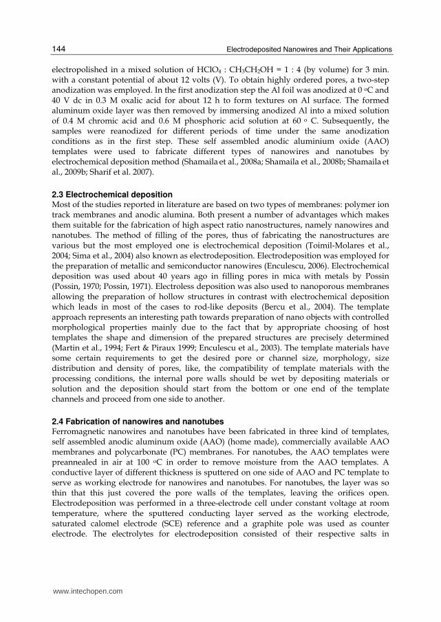
Fig. 1. (a) AFM top view (0.5x0.5 µm2); (b-d) SEM image of (b) homemade AAO templates (anodized in 0.3M oxalic acid solution) with diameter, d ~ 40 nm, (c) homemade (anodized in 5%H3PO4 solution) and (d) commercial AAO templates with diameter, d ~ 200 nm.
Figure 1 shows (a) AFM top view (1x1 µm2) (b) SEM view of homemade anodic alumina (AAO) template prepared by two-step anodization in 0.3 M oxalic acid, with diameter equal to 40 nm; (c) homemade AAO template anodized in 5% phosphoric acid and (d) Commercial AAO templates, with diameter equal to 200 nm. The fabricated AAO t emplates contain self-assembled uniform pore arrays with quasi-hexagonal ordering. The average centre-to-centre spacing (Di) and pore diameter (d) depend on anodization conditions and the electrolyte used for anodization. Generally, pore diameter of AAO film is increased if the anodized voltage is large, and length (L) of the pores is increased with time for anodization.
www.intechopen.com
Electrodeposited Nanowires and Their Applications
146
Figure 1a-d shows that our home made AAO templates are highly uniform and ordered as compare to the commercially available anodic alumina membranes as shown in Figure 1d.
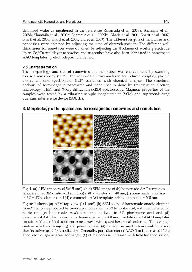
Fig. 2. SEM images of isolated (a) Co, (b) Ni, (c) CoPt, and (d) CoCrPt, Nanowires separated from AAO template by dissolving the alumina layer in NaOH aqueous solution.
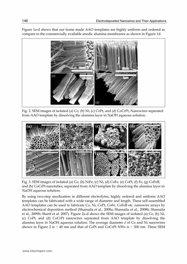
Fig. 3. SEM images of isolated (a) Co, (b) NiFe, (c) Ni, (d) CoFe, (e) CoPt, (f) Fe, (g) CoFeB, and (h) CoCrPt nanotubes, separated from AAO template by dissolving the alumina layer in NaOH aqueous solution.
By using two-step anodization in different electrolytes, highly ordered and uniform AAO templates can be fabricated with a wide range of diameter and length. These self-assembled AAO templates can be used to fabricate Co, Ni, CoPt, CoFe, CoFeB etc. nanowire arrays by electrochemical deposition method (Shamaila et al., 2008a; Shamaila et al., 2008b; Shamaila et al., 2009b; Sharif et al. 2007). Figure 2a-d shows the SEM images of isolated (a) Co, (b) Ni, (c) CoPt, and (d) CoCrPt nanowires separated from AAO template by dissolving the alumina layer in NaOH aqueous solution. The average diameter d of Co and Ni nanowires shown in Figure 2 is ~ 40 nm and that of CoPt and CoCrPt NWs is ~ 200 nm. These SEM
www.intechopen.com
Ferromagnetic Nanowires and Nanotubes
147
images reveal that nanowires of several materials with different diameters can be fabricated by using the templates of different diameters.
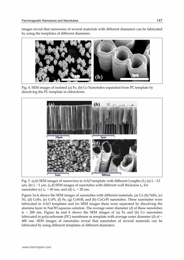
Fig. 4. SEM images of isolated (a) Fe, (b) Co Nanotubes separated from PC template by dissolving the PC template in chloroform.
Fig. 5. (a,b) SEM images of nanowires in AAO template with different Lengths (L) (a) L ~12 µm, (b) L ~1 µm. (c,d) SEM images of nanotubes with different wall thickness tw for nanotubes (c) tw ~ 60 nm, and (d) tw ~ 20 nm.
Figure 3a-h shows the SEM images of nanotubes with different materials, (a) Co (b) NiFe, (c) Ni, (d) CoFe, (e) CoPt, (f) Fe, (g) CoFeB, and (h) CoCrPt nanotubes. These nanotubes were fabricated in AAO templates and for SEM images these were separated by dissolving the alumina layer in NaOH aqueous solution. The average outer diameter (d) of these nanotubes is ~ 200 nm. Figure 4a and b shows the SEM images of (a) Fe and (b) Co nanotubes fabricated in polycarbonate (PC) membrane as template with average outer diameter (d) of ~ 400 nm. SEM images of nanotubes reveal that nanotubes of several materials can be fabricated by using different templates of different diameters.
www.intechopen.com
Electrodeposited Nanowires and Their Applications
148
Figure 5a-d shows the SEM images of nanocylinders with (a and b) different lengths (L) for nanowires (a) L~12 µm, (b) L~ 1 µm and (c and d) different wall thickness tw for nanotubes (c) tw ~ 60 nm, and (d) tw ~ 20 nm. Since the nanocylinders are characterized geometrically by their length (L), external and internal diameter (d & a) respectively, and wall thickness (tw), where tw =0 gives nanowire and tw > 0 gives nanotube geometry. This tw makes the nanotubes distinct from that of nanowires and strongly affects the magnetization reversal mechanism and thereby, the overall magnetic behaviour (Escrig et al., 2008). These SEM images reveal that nanowires with wide range of diameter and lengths, and nanotubes with different external and internal diameter, length and wall thickness can be fabricated by low cost electrodeposition method.
4. Structural characterizations of ferromagnetic nanowires and nanotubes
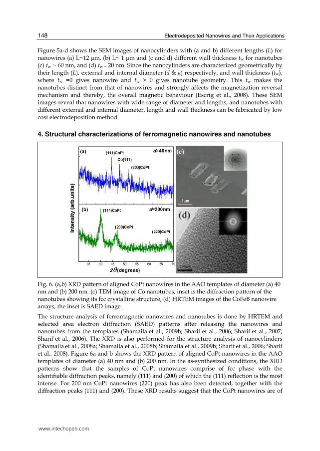
Fig. 6. (a,b) XRD pattern of aligned CoPt nanowires in the AAO templates of diameter (a) 40 nm and (b) 200 nm. (c) TEM image of Co nanotubes, inset is the diffraction pattern of the nanotubes showing its fcc crystalline structure, (d) HRTEM images of the CoFeB nanowire arrays, the inset is SAED image.
The structure analysis of ferromagnetic nanowires and nanotubes is done by HRTEM and selected area electron diffraction (SAED) patterns after releasing the nanowires and nanotubes from the templates (Shamaila et al., 2009b; Sharif et al., 2006; Sharif et al., 2007; Sharif et al., 2006). The XRD is also performed for the structure analysis of nanocylinders (Shamaila et al., 2008a; Shamaila et al., 2008b; Shamaila et al., 2009b; Sharif et al., 2006; Sharif
et al., 2008). Figure 6a and b shows the XRD pattern of aligned CoPt nanowires in the AAO templates of diameter (a) 40 nm and (b) 200 nm. In the as-synthesized conditions, the XRD patterns show that the samples of CoPt nanowires comprise of fcc phase with the identifiable diffraction peaks, namely (111) and (200) of which the (111) reflection is the most intense. For 200 nm CoPt nanowires (220) peak has also been detected, together with the diffraction peaks (111) and (200). These XRD results suggest that the CoPt nanowires are of
www.intechopen.com
Ferromagnetic Nanowires and Nanotubes
149
fcc polycrystalline structure with randomly oriented grains. Figure 6c is the TEM image of Co nanotubes. The inset shows diffraction pattern of the nanotubes showing its fcc crystalline structure. Figure 6d exhibits the HRTEM images of the CoFeB nanowire arrays, the inset is SAED image which show amorphous phase for CoFeB nanowire arrays. Structural analysis explores that nanowires and nanotubes of crystalline and amorphous structure for different kinds of nanocylinders. Structural analysis understanding can be used to fabricate crystalline or amorphous nanowires and nanotubes according to the required applications.
5. Magnetic and magnetization properties of nanowires and nanotubes
No. Composition Hc// (Oe) Hc⊥ (Oe) SQ// SQ⊥ Ref
1 Fe 89 125 0.02 0.05 In this work
2 Co 863 300 0.57 0.11 Shamaila et al.2009b
3 Ni 230 105 0.22 0.06 Han et al.2003
4 Ni86Fe14 769 313 0.65 0.12 Hao et al.2001
5 Co94Fe6 66 111 0.01 0.03 Sharif et al.2008b
6 Co90Pt10 105 80 0.02 0.04 In this work
7 Co91Fe7B3 208 265 0.08 0.07 Sharif et al.2008b
8 Co75Cr13Pt12 121 233 0.09 0.32 Shamaila et al.2009a
Table 1. Ferromagnetic nanowires in AAO template (L > 10 μm)
No. Composition Hc// (Oe) Hc⊥ (Oe) SQ// SQ⊥ Ref
1 Fe 364 163 0.09 0.35 In this work
2 Co 115 75 0.03 0.05 In this work
3 Ni 111 102 0.16 0.24 In this work
4 Ni93Fe7 57 63 0.02 0.25 In this work
5 Co94Fe6 107 192 In this work
6 Co90Pt10 125 177 0.06 0.09 In this work
7 Co80Fe17B3 353 108 0.04 0.4 In this work
8 Co75Cr13Pt12 251 135 0.03 0.13 Shamaila et al.2009a
Table 2. Ferromagnetic nanotubes in AAO template (L > 10 μm)
Table I shows the magnetic properties of metal nanowires like Fe, Co, and Ni and alloy NiFe, CoFe, CoPt, CoFeB, and CoCrPt nanowire arrays fabricated by electrodeposition in AAO template. Table II shows the magnetic properties of metal nanotubes like Fe, Co, and Ni and alloy NiFe, CoFe, CoPt, CoFeB, and CoCrPt nanotube arrays fabricated by electrodeposition in AAO template (Shamaila et al., 2008a; Shamaila et al., 2008b; Shamaila et al., 2009a; Shamaila et al., 2009b; Sharif et al., 2006; Sharif et al., 2007; Sharif et al., 2008a; Sharif et al., 2008b). Table III shows the magnetic properties of metal nanotubes like Fe, Co, and Ni nanotube arrays fabricated by electrodeposition in polycarbonate (PC) template. The magnetic properties of pure and alloy nanowire and nanotube arrays in AAO and PC templates can be compared from these tables. Because of the intrinsic properties difference
www.intechopen.com
Electrodeposited Nanowires and Their Applications
150
between different metals and their alloys, the demagnetization field (2πMs) of individual
cylinders (for infinite cylinder) and dipolar interaction among the nanocylinders will be different. Therefore their properties are different from each other.
No. Composition Hc// (Oe) Hc⊥ (Oe) SQ// SQ⊥ Ref
1 Fe 145 149 0.05 0.22 Sharif et al.2008a
2 Co 158 197 0.11 0.37 Sharif et al.2008a
3 Ni 80 127 0.06 0.31 Sharif et al.2008a
Table 3. Ferromagnetic nanotubes in Polycarbonate (PC) template (L ~ 6 μm)
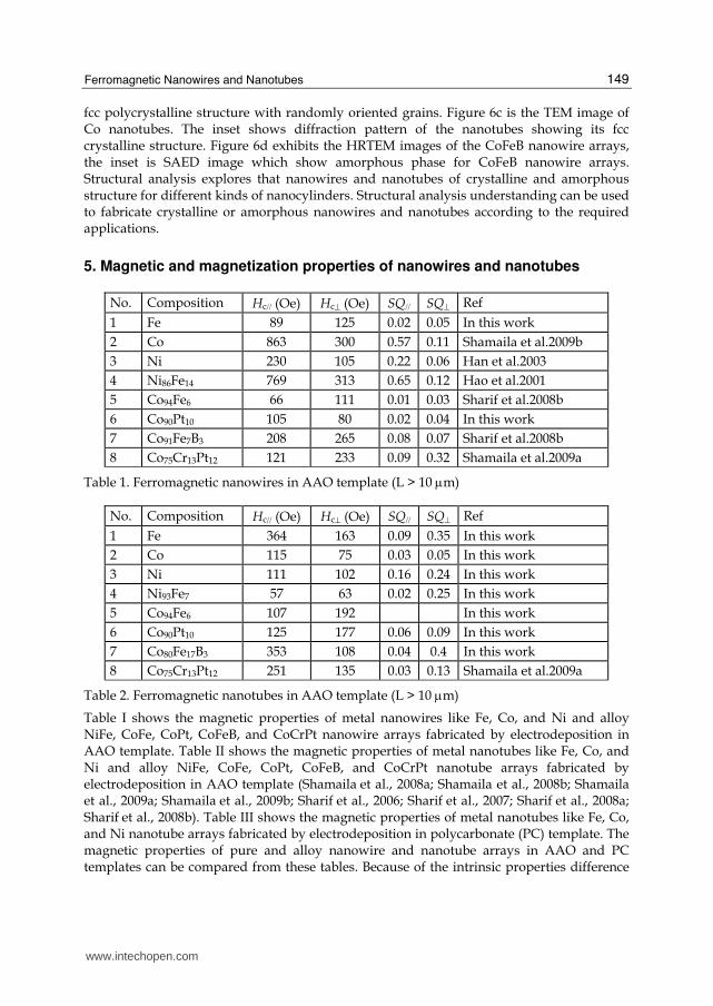
5.1 Easy axis of ferromagnetic nanowires
Fig. 7. M-H curves for CoPt nanowire arrays of diameter (a) 40 nm and (b) 200 nm shows the crossover of easy axis as a function of diameter.
Shape and geometry dependent magnetization behaviour of the CoPt nanowires and nanotubes is explained here. Diameter and length have strong effects on the magnetic properties of nanocylinder. The typical room temperature magnetic hysteresis (M-H) curves for 40 and 200 nm CoPt nanowires, with the external field applied parallel and perpendicular to the nanowire axis, are shown in Figure 7a and b. The difference between the perpendicular and parallel M-H curves defines the uniaxial anisotropy for CoPt nanowire arrays. For 40 nm CoPt nanowires (Figure 7a) the remanent squareness (SQ) in the
parallel (⁄⁄) geometry is larger than that of the perpendicular (⊥) geometry attributing to the parallel alignment of the magnetic easy axis along the wire axis (Mallet et al., 2004). For 200 nm CoPt nanowires as shown in Figure 7b, SQ in the perpendicular geometry is larger than that of the parallel geometry. Therefore the easy axis of magnetic anisotropy favours to be aligned perpendicular to the wire axis. This variation in the alignment of easy axis for the two diameters shows a crossover of easy axis of magnetization as a function of diameter. The values of magnetic parameters Hc, SQ and alignment of easy axis for different diameters and lengths are presented in Table IV. Comparison of the parameters, given in Table IV shows the effect of the diameter and length on the magnetic properties of CoPt nanowire and nanotube arrays. The alignment of easy axis can also be specified by the sign of difference of saturation fields (∆Hs) here ∆Hs = Hs⁄⁄ -
Hs⊥ (Ciureanu et al., 2005). Here Hs⁄⁄ is the saturation field when magnetic field is applied
www.intechopen.com
Ferromagnetic Nanowires and Nanotubes
151
parallel to the nanocylinder axis and Hs⊥ is the saturation field when the magnetic field is applied perpendicular to the nanocylinder axis. Negative sign of ∆Hs indicates the easy axis along the nanocylinder axis and positive sign shows the orientation of easy axis perpendicular to the nanocylinder axis.
No Diameter
(nm)
Length
(μm) Hc// (Oe)
Hc⊥ (Oe)
SQ// SQ⊥ ΔHs Easy axis
Ref.
1 40 2 2033 575 0.93 0.15 -2164.45 // Shamaila et al.2009a
2 40 20 1051 555 0.84 0.21 -3375.59 // Shamaila et al.2009a
3 200 0.8 652 303 0.38 0.14 -717.45 // Shamaila et al.2009a
4 200 10 189 141 0.07 0.18 4018.07 ⊥ Shamaila et al.2009a
Table 4. Effect of Length on the easy axis of ferromagnetic Co90Pt10 nanowires in AAO template
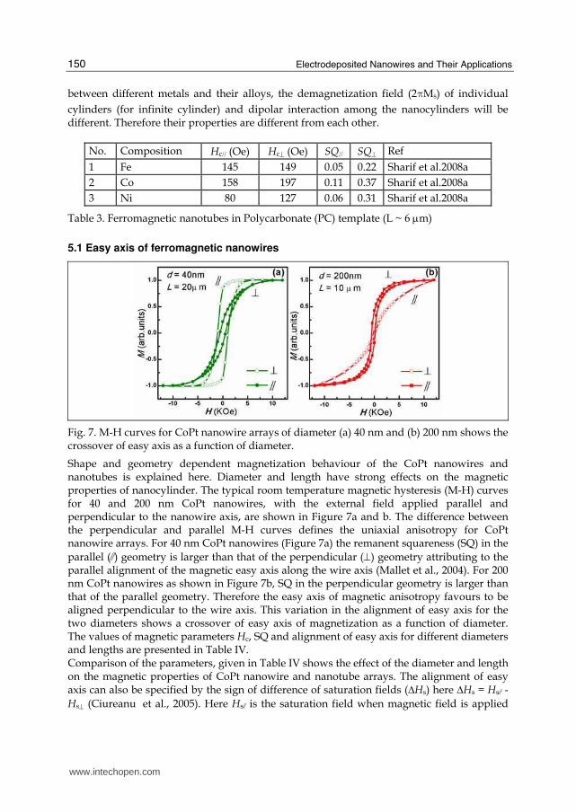
Fig. 8. M-H curves for CoPt nanowire arrays with length (a) 0.8 µm and (b) 10 µm shows the cross over of easy axis as a function of length.
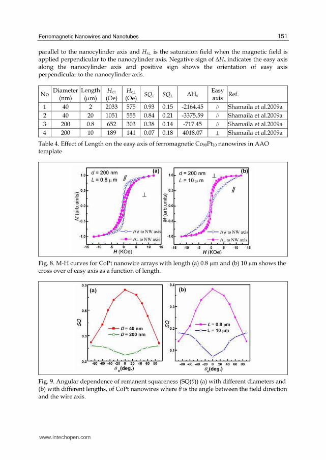
Fig. 9. Angular dependence of remanent squareness (SQ(θ)) (a) with different diameters and (b) with different lengths, of CoPt nanowires where θ is the angle between the field direction and the wire axis.
www.intechopen.com
Electrodeposited Nanowires and Their Applications
152
Figure 8a-b show the effect of length on the magnetic properties of CoPt nanowire arrays for
diameter d ~ 200 nm. Figure 8a-b show that parallel magnetization is favoured for very short
nanowires whereas; perpendicular magnetization is favoured for long nanowires. Thus, in
CoPt nanowires, it is observed that when the wire length is larger than a critical value, the
parallel wire axis crosses over from easy to hard as also was observed by others for Co
nanowire arrays (Rivas et al., 2002). This crossover is clear from the shape of M-H curves as
well as from the sign of Delta Hs (Table 4) of these samples. This effect can be used to turn
the parallel wire axis from easy to hard, by modifying the length. Additional evidence for
the crossover of easy axis is provided by the angular dependence of the SQ of CoPt
nanowire arrays measured as a function of wire diameter and length (Figure 9). SQ(θ) curves show bell-shaped or otherwise bell-shaped behaviour corresponding to the easy axis
of their magnetization. Bell-shaped curves for sample with d = 40 nm and otherwise bell-
shaped curve for sample with d = 200 nm confirms the crossover of easy axis from parallel to
perpendicular as a function of diameter (Figure 9a). Furthermore, bell-shaped behaviour of
sample with d = 200 nm, and length = 0.8 µm with the easy axis parallel to the wire axis and
otherwise bell-shaped curve for sample with length = 10 µm with easy axis perpendicular to
the wire axis shows the crossover of easy axis as a function of length. Figure 9a and b also
show that values for SQ for samples with d = 40 nm are larger than sample of 200 nm.
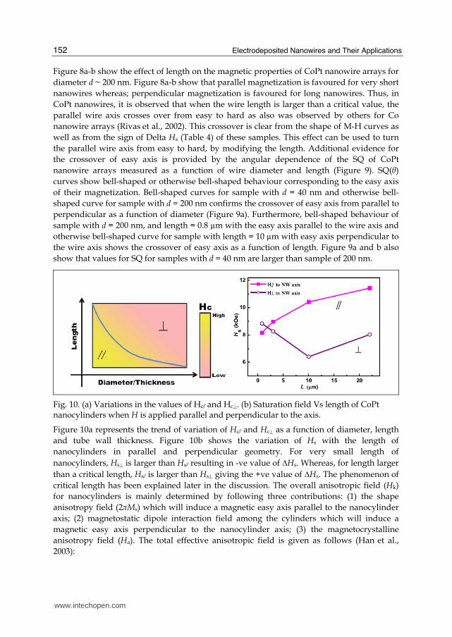
Fig. 10. (a) Variations in the values of Hc⁄⁄ and Hc⊥. (b) Saturation field Vs length of CoPt nanocylinders when H is applied parallel and perpendicular to the axis.
Figure 10a represents the trend of variation of Hc⁄⁄ and Hc⊥ as a function of diameter, length
and tube wall thickness. Figure 10b shows the variation of Hs with the length of
nanocylinders in parallel and perpendicular geometry. For very small length of
nanocylinders, Hs⊥ is larger than Hs⁄⁄ resulting in -ve value of ∆Hs. Whereas, for length larger
than a critical length, Hs⁄⁄ is larger than Hs⊥ giving the +ve value of ∆Hs. The phenomenon of
critical length has been explained later in the discussion. The overall anisotropic field (Hk)
for nanocylinders is mainly determined by following three contributions: (1) the shape
anisotropy field (2πMs) which will induce a magnetic easy axis parallel to the nanocylinder
axis; (2) magnetostatic dipole interaction field among the cylinders which will induce a
magnetic easy axis perpendicular to the nanocylinder axis; (3) the magnetocrystalline
anisotropy field (Ha). The total effective anisotropic field is given as follows (Han et al.,
2003):
www.intechopen.com
Ferromagnetic Nanowires and Nanotubes
153
Hk = 2πMs - 6.3πMs r2L / D3 + Ha (1)
Where Ms is the saturation magnetization, r is the radius of the wire, L is the length and D is the interwire distance. The second term in Eq.1 is the total dipole field acting on one wire due to all other wires. Eq.1 predicts that as the wire length increases, Hk linearly decreases to zero when
L =Lc = 2D3 / 6.3r2 (2)
while neglecting the contribution of Ha. For L>Lc, Hk is negative pointing out that there is a crossover of easy axis for magnetization from parallel to perpendicular to the axis. For CoPt nanowire arrays with d = 200 nm, r = 100 nm and D = 250 nm; Lc ~ 1 µm is calculated. The shape anisotropy field is weak in this case therefore when L>Lc, Hk is negative and crossover of easy axis of magnetization from parallel to perpendicular to nanowire axis is observed. The orientation of easy axis of magnetization can be determined by the total energy ∑E in the parallel and perpendicular geometries where ∑E can be obtained by taking into account the magnetostatic interaction energy Emi, the demagnetization energy Ede, the
magnetocrystalline anisotropy Ek, where Emi⁄⁄ > Emi⊥, Ede⁄⁄ < Ede⊥, Ek⁄⁄ < Ek⊥ (Gao et al., 2006). For large diameters with small interwire distances, the dipolar interaction is increased, ∑E⁄⁄ ~
∑E⊥ and the easy axis favors to be aligned perpendicular to the wire axis (Rivas, 2002). For
small diameters, ∑E⁄⁄ < ∑E⊥ and the easy axis favors to be aligned along the cylinder axis. It should also be pointed that other reasons cannot be excluded such as the orientation of crystallographic axes and grain size of the nanocylinders. A wide range of values of Hc (from Hc⁄⁄ = 2032 Oe for d = 40 nm to Hc⁄⁄ = 100 Oe for d = 200 nm) and SQ (from SQ⁄⁄ = 0.93 for d = 40 nm to SQ⁄⁄ = 0.07 for d = 200 nm) is observed depending upon different factors involved in the magnetic properties of the CoPt nanocylinders. The results discussed here reveal that ferromagnetic nanocylinders with easy axis of magnetization either parallel or perpendicular to the nanocylinder axis having the desired values of Hc and SQ for perpendicular recording media can be obtained by modifying the diameter, length or geometry of the nanocylinders.
5.2 Magnetization reversal mechanism The two most common magnetization reversal modes can be modeled by coherent rotation
or curling. Generally for magnetic nanowires the magnetization reversal mechanism
depends upon the diameter of the nanowires. For a specific material, the critical diameter for
the transition from coherent rotation to non-coherent rotation is given by
dc = 2.08 (A1/2 / Ms) (3)
where A is the exchange stiffness and Ms is the saturation magnetization (Zeng et al., 2002).
5.3 Coherent rotation model In presence of coherent rotation mode in one isolated nanocylinder, the micro-spin
configuration in the system should be uniformly magnetized with the external applied field
as shown in Figure 11a. If the nanocylinders are of soft magnetic material, the crystal
anisotropy can be neglected safely. Thus, only the shape anisotropy is contributed to the
reversal mechanism. The magnetization can be easily modeled by mz = cos(θ). Hence the
total energy is given by
www.intechopen.com
Electrodeposited Nanowires and Their Applications
154
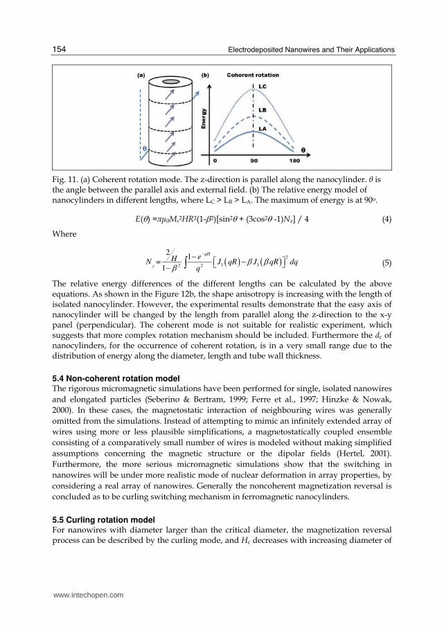
Fig. 11. (a) Coherent rotation mode. The z-direction is parallel along the nanocylinder. θ is the angle between the parallel axis and external field. (b) The relative energy model of nanocylinders in different lengths, where LC > LB > LA. The maximum of energy is at 90o.
E(θ) =πμ0Ms2HR2(1-β2)[sin2θ + (3cos2θ -1)Nz] / 4 (4)
Where
( ) ( ) 2
1 12 2
21
=1Z
qHeHN J qR J qR dqq
β ββ−− −⎡ ⎤⎣ ⎦− ∫
(5)
The relative energy differences of the different lengths can be calculated by the above equations. As shown in the Figure 12b, the shape anisotropy is increasing with the length of isolated nanocylinder. However, the experimental results demonstrate that the easy axis of nanocylinder will be changed by the length from parallel along the z-direction to the x-y panel (perpendicular). The coherent mode is not suitable for realistic experiment, which suggests that more complex rotation mechanism should be included. Furthermore the dc of nanocylinders, for the occurrence of coherent rotation, is in a very small range due to the distribution of energy along the diameter, length and tube wall thickness.
5.4 Non-coherent rotation model The rigorous micromagnetic simulations have been performed for single, isolated nanowires
and elongated particles (Seberino & Bertram, 1999; Ferre et al., 1997; Hinzke & Nowak,
2000). In these cases, the magnetostatic interaction of neighbouring wires was generally
omitted from the simulations. Instead of attempting to mimic an infinitely extended array of
wires using more or less plausible simplifications, a magnetostatically coupled ensemble
consisting of a comparatively small number of wires is modeled without making simplified
assumptions concerning the magnetic structure or the dipolar fields (Hertel, 2001).
Furthermore, the more serious micromagnetic simulations show that the switching in
nanowires will be under more realistic mode of nuclear deformation in array properties, by
considering a real array of nanowires. Generally the noncoherent magnetization reversal is
concluded as to be curling switching mechanism in ferromagnetic nanocylinders.
5.5 Curling rotation model For nanowires with diameter larger than the critical diameter, the magnetization reversal process can be described by the curling mode, and Hc decreases with increasing diameter of
www.intechopen.com
Ferromagnetic Nanowires and Nanotubes
155
the nanowires. For example the critical diameter for CoPt nanowires was calculated as dc=14 nm (Mallet et al., 2004). The equation describing the dependence of Hc on the diameter of nanowires in the curling mode has been given as follows (Mallet et al., 2004),
2
2 1 2 uc
s s
kA KH
M r M
π= + (6)
where r is the radius of the nanowire and k is a constant related to the shape of the material
(1.08 for an infinite cylinder.) Ku is the uniaxial anisotropy constant. To certain extent, the
relation of Hc and dc can also be generalized for nanotubes under curling mode.
5.6 Angular dependent rotation mode
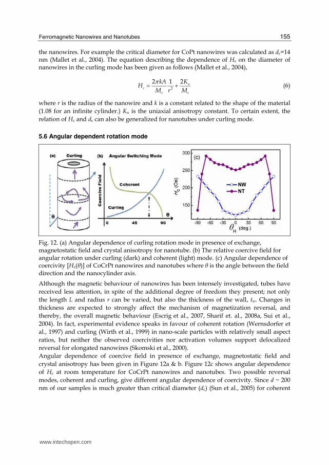
Fig. 12. (a) Angular dependence of curling rotation mode in presence of exchange, magnetostatic field and crystal anisotropy for nanotube. (b) The relative coercive field for angular rotation under curling (dark) and coherent (light) mode. (c) Angular dependence of coercivity [Hc(θ)] of CoCrPt nanowires and nanotubes where θ is the angle between the field direction and the nanocylinder axis.
Although the magnetic behaviour of nanowires has been intensely investigated, tubes have
received less attention, in spite of the additional degree of freedom they present; not only
the length L and radius r can be varied, but also the thickness of the wall, tw. Changes in
thickness are expected to strongly affect the mechanism of magnetization reversal, and
thereby, the overall magnetic behaviour (Escrig et al., 2007, Sharif et. al., 2008a, Sui et al.,
2004). In fact, experimental evidence speaks in favour of coherent rotation (Wernsdorfer et
al., 1997) and curling (Wirth et al., 1999) in nano-scale particles with relatively small aspect
ratios, but neither the observed coercivities nor activation volumes support delocalized
reversal for elongated nanowires (Skomski et al., 2000).
Angular dependence of coercive field in presence of exchange, magnetostatic field and
crystal anisotropy has been given in Figure 12a & b. Figure 12c shows angular dependence
of Hc at room temperature for CoCrPt nanowires and nanotubes. Two possible reversal
modes, coherent and curling, give different angular dependence of coercivity. Since d ~ 200
nm of our samples is much greater than critical diameter (dc) (Sun et al., 2005) for coherent
www.intechopen.com
Electrodeposited Nanowires and Their Applications
156
rotation, therefore, reversal mechanism is expected to occur through curling rotation. The
curling mode of reversal mechanism for nanocylinders predicts that
( )( )2 2
1=
1 2 cosc k
a aH H
a a θ+
+ +
(7)
where a =-1.08 (dc /d)2 (Han et al., 2003). Eq.7 describes that Hc increases as angle (θ) increases, whereas coherent rotation mode predicts that Hc decreases as angle increases (Han et al., 2003, Sun et al., 2005). For CoCrPt nanowires, Hc increases with increasing angle
θ from 0o to ± 90o representing curling mode of reversal mechanism. Hc of nanotubes
initially increases with increasing angle up to θ = ± 70o, in good agreement with the curling model; however, above this critical angle Hc decreases abruptly expressing an M-type variation. M-type curve for nanotubes (Figure 12c) reveal that at large angles, coherent
rotation is dominant, while curling happens only for small angles (θ ≤ 70o). The distinct geometry of nanotubes presents two dynamic configurations of magnetic moments with the applied field. When the field angle is small the magnetic moments will align preferably parallel to the tube axis and reversal will take place by curling rotation. At large field angles the moments will align perpendicular to tube axis and coherent reversal mode will be observed. Different alignment of moments and surface effects due to tw in nanotubes are causes of transition from curling to coherent reversal mechanism for higher angles. The transition angle depends on d and tw of nanotubes as previously proved theoretically for other nanotubes (Escrig et al., 2008). Our experimental data is in accordance with the trend given in Figure 12a & b. However, the angular dependence of various ferromagnetic nanocylinders to understand the insights of magnetization switching requires some further explanations. Further understanding describes that the curling rotation mechanism can be adopted more generally for nanowires only whereas for nanotubes curling mechanism is influenced by some other phenomenon which are explained in detail discussion given below.
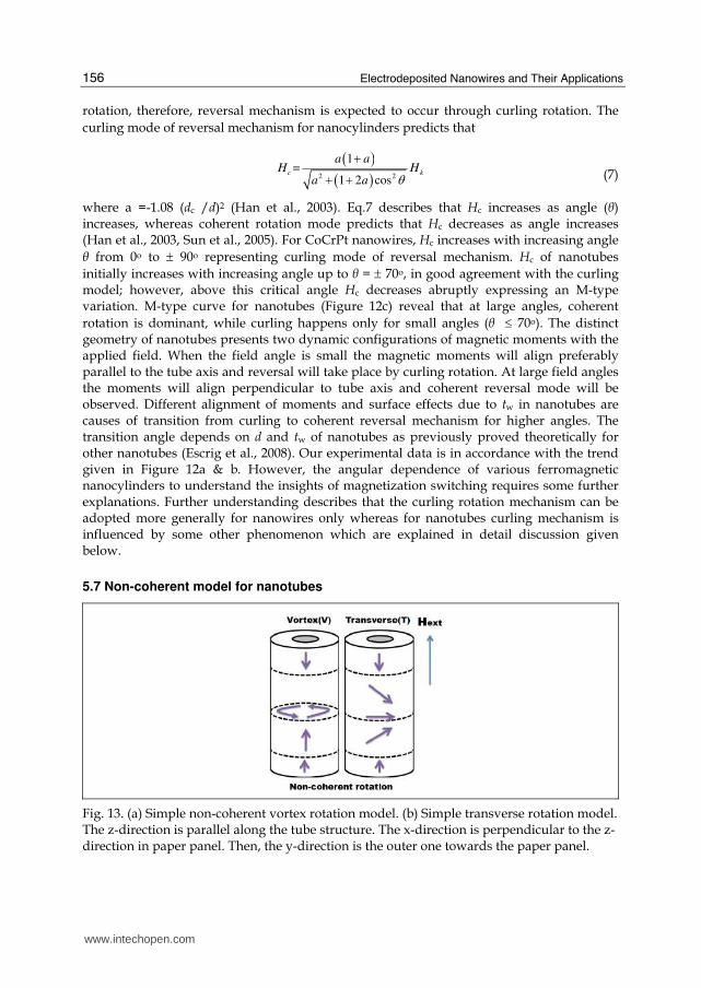
5.7 Non-coherent model for nanotubes
Fig. 13. (a) Simple non-coherent vortex rotation model. (b) Simple transverse rotation model. The z-direction is parallel along the tube structure. The x-direction is perpendicular to the z-direction in paper panel. Then, the y-direction is the outer one towards the paper panel.
www.intechopen.com
Ferromagnetic Nanowires and Nanotubes
157
The underline physics of the non-coherent rotation is in the dynamic field-driven domain
wall motion in the isolated nanocylinder. Considering the simplest cases of parallel
switching in the isolated nanotubes, two switching mechanisms can be idealized for the
propagation of domain wall in ferromagnetic nanotubes, one is vortex domain wall and
another is transverse domain wall motion, as shown in Figure 13a and b and in reference
(Landeros et al., 2007). Starting from the equations presented by Landeros for the vortex
mode V, the magnetization is a little complex spin closure structure along the tube wall. For
the transverse mode T, the magnetization of domain wall is the several coherent rotations in
y-z panel. In both cases, the switching along z-direction is the domain motion at one end of
the tube and propagates toward the other, as illustrated in Figure 13. Using the equations
presented by Landeros (Landeros et al., 2007), the zero-field energy barrier as well as the
width of the domain for each reversal model as a function of the tube wall thickness can be
calculated. For the vortex rotation model the micro-spin configuration could be modeled by,
m(z) = { ( ) ( )ˆ, 0 / 2
ˆ ˆ, / 2 / 2
ˆ, / 2 .
w
z w w
w
z z z w
m z m z z z w z z w
z z w z L
φ φ≤ ≤ −
+ − < < +− + ≤ ≤
(8)
Where mz(z)=cosΘ(z), Θ(z) = Π((z-zw)/w+1/2) and mx = - mφ(z)sinφ, my = --mφ(z)cosφ. The
transverse domain is only different at the description of magnetization within the region of
transverse domain wall. Which can be described as ( ) ( ) ( ) ( ) ( )ˆ ˆ, cosx x zm z m z x m z z m z z= + = Θ .
The zw is the position at the centre of domain wall. Then, by considering the crystal
anisotropy, shape anisotropy and exchange interactions, the energy barrier can be calculated
by integral of the spacial magnetization structures. The general tendency of the calculation
results have been reported (Landeros et al., 2007).
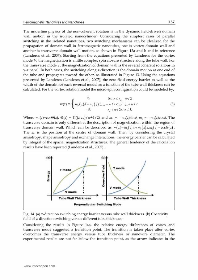
Fig. 14. (a) z-direction switching energy barrier versus tube wall thickness. (b) Coercivity field of z-direction switching versus different tube thickness.
Considering the results in Figure 14a, the relative energy differences of vortex and transverse mode suggested a transition point. The transition is taken place after vortex overcomes the transverse energy versus tube thickness or nanowire diameter. The experimental results are not far below the transition point, as the arrow indicates in the
www.intechopen.com
Electrodeposited Nanowires and Their Applications
158
Figure 14a, while, the Figure 14 implicates an increase of coercivity under vortex mode. But the cross over in Figure 14b does not mean the transition from vortex switching to transverse. In our experimental results presented in the tables and above discussion, we usually observe vortex-like curling mode. In perfect ellipsoids of revolution subject to a field parallel to the long axis, magnetization reversal starts by coherent rotation or curling, although there remains a remote possibility of a buckling mode (Aharoni, 1996). The transition between the two modes depends on the radius of the ellipsoid similar to that of dc in case of nanocylinders. Although the above explanations can generally model our experimental results, the more rigorous switching modes in case of presenting nanocylinder array properties is a little different in dynamic mechanism as will be discussed below.
5.8 Magnetostatic interactions of ferromagnetic nanocylinder array
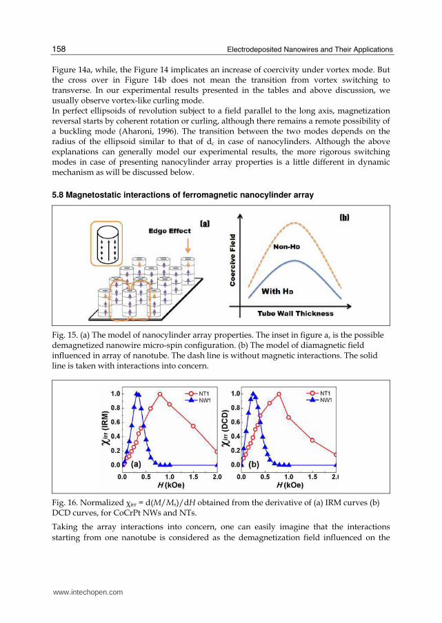
Fig. 15. (a) The model of nanocylinder array properties. The inset in figure a, is the possible demagnetized nanowire micro-spin configuration. (b) The model of diamagnetic field influenced in array of nanotube. The dash line is without magnetic interactions. The solid line is taken with interactions into concern.
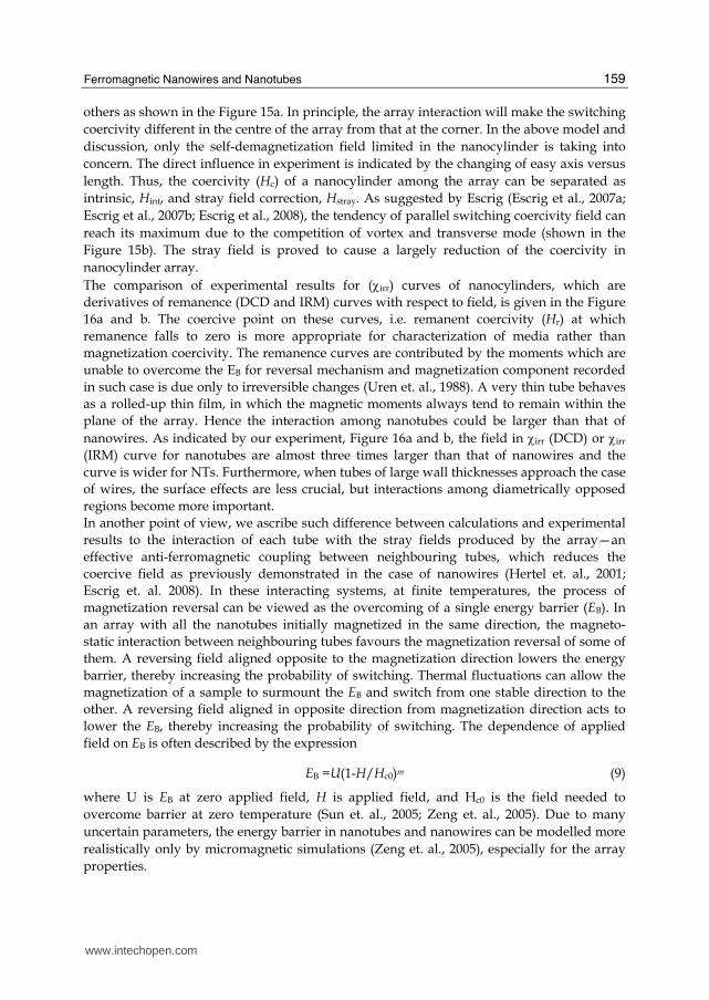
Fig. 16. Normalized χirr = d(M/Ms)/dH obtained from the derivative of (a) IRM curves (b) DCD curves, for CoCrPt NWs and NTs.
Taking the array interactions into concern, one can easily imagine that the interactions
starting from one nanotube is considered as the demagnetization field influenced on the
www.intechopen.com
Ferromagnetic Nanowires and Nanotubes
159
others as shown in the Figure 15a. In principle, the array interaction will make the switching
coercivity different in the centre of the array from that at the corner. In the above model and
discussion, only the self-demagnetization field limited in the nanocylinder is taking into
concern. The direct influence in experiment is indicated by the changing of easy axis versus
length. Thus, the coercivity (Hc) of a nanocylinder among the array can be separated as
intrinsic, Hint, and stray field correction, Hstray. As suggested by Escrig (Escrig et al., 2007a;
Escrig et al., 2007b; Escrig et al., 2008), the tendency of parallel switching coercivity field can
reach its maximum due to the competition of vortex and transverse mode (shown in the
Figure 15b). The stray field is proved to cause a largely reduction of the coercivity in
nanocylinder array.
The comparison of experimental results for (χirr) curves of nanocylinders, which are
derivatives of remanence (DCD and IRM) curves with respect to field, is given in the Figure
16a and b. The coercive point on these curves, i.e. remanent coercivity (Hr) at which
remanence falls to zero is more appropriate for characterization of media rather than
magnetization coercivity. The remanence curves are contributed by the moments which are
unable to overcome the EB for reversal mechanism and magnetization component recorded
in such case is due only to irreversible changes (Uren et. al., 1988). A very thin tube behaves
as a rolled-up thin film, in which the magnetic moments always tend to remain within the
plane of the array. Hence the interaction among nanotubes could be larger than that of
nanowires. As indicated by our experiment, Figure 16a and b, the field in χirr (DCD) or χirr
(IRM) curve for nanotubes are almost three times larger than that of nanowires and the
curve is wider for NTs. Furthermore, when tubes of large wall thicknesses approach the case
of wires, the surface effects are less crucial, but interactions among diametrically opposed
regions become more important.
In another point of view, we ascribe such difference between calculations and experimental
results to the interaction of each tube with the stray fields produced by the array—an
effective anti-ferromagnetic coupling between neighbouring tubes, which reduces the
coercive field as previously demonstrated in the case of nanowires (Hertel et. al., 2001;
Escrig et. al. 2008). In these interacting systems, at finite temperatures, the process of
magnetization reversal can be viewed as the overcoming of a single energy barrier (EB). In
an array with all the nanotubes initially magnetized in the same direction, the magneto-
static interaction between neighbouring tubes favours the magnetization reversal of some of
them. A reversing field aligned opposite to the magnetization direction lowers the energy
barrier, thereby increasing the probability of switching. Thermal fluctuations can allow the
magnetization of a sample to surmount the EB and switch from one stable direction to the
other. A reversing field aligned in opposite direction from magnetization direction acts to
lower the EB, thereby increasing the probability of switching. The dependence of applied
field on EB is often described by the expression
EB =U(1-H/Hc0)m (9)
where U is EB at zero applied field, H is applied field, and Hc0 is the field needed to
overcome barrier at zero temperature (Sun et. al., 2005; Zeng et. al., 2005). Due to many
uncertain parameters, the energy barrier in nanotubes and nanowires can be modelled more
realistically only by micromagnetic simulations (Zeng et. al., 2005), especially for the array
properties.
www.intechopen.com
Electrodeposited Nanowires and Their Applications
160
6. Concluding remarks
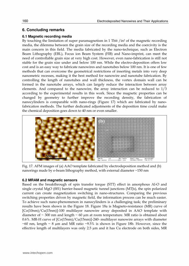
6.1 Magnetic recording media By touching the limitation of super paramagnetism in 1 Tbit /in2 of the magnetic recording media, the dilemma between the grain size of the recording media and the coercivity is the main concern in this field. The media fabricated by the nano-technique, such as Electron Beam Lithography (EBL), Focus ion Beam System (FIB) and Nano-imprint, can meet the need of controllable grain size at very high cost. However, even nano-fabrication is still not stable for the grain size under and below 100 nm. While the electro-deposition offers low cost and is an easy way to fabricate nanowires and nanotubes below 100 nm. It is one of few methods that can overcome the geometrical restrictions of inserting metals into very deep nanometric recesses, making it the best method for nanowire and nanotube fabrication. By controlling the length of nanotubes and wall thickness, the vortex domain wall can be formed in the nanotube arrays, which can largely reduce the interaction between array elements. And compared to the nanowire, the array interaction can be reduced to 1/3 according to the experimental results in this work. Since the magnetic properties can be changed by geometry to further improve the recording density, the fabrication of nanocylinders is comparable with nano-rings (Figure 17) which are fabricated by nano-fabrication methods. The further dedicated adjustments of the deposition time could make the chemical deposition goes down to 40 nm or even smaller.
Fig. 17. AFM images of (a) AAO template fabricated by electrodeposition method and (b) nanorings made by e-beam lithography method, with external diameter ~150 nm
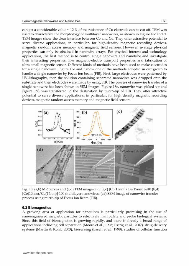
6.2 MRAM and magnetic sensors Based on the breakthrough of spin transfer torque (STT) effect in amorphous Al-O and single crystal MgO (001) barrier-based magnetic tunnel junctions (MTJs), the spin polarized current can create magnetization switching in nano-structures. Comparing the previous switching properties driven by magnetic field, the information process can be much easier. To achieve such nano-phenomenon in nanocylinders is a challenging task; the preliminary results have been shown in the Figure 18. Figure 18a is Magneto-resistance (MR) curve of [Co(10nm)/Cu(15nm)]-100 multilayer nanowire array deposited in AAO template with diameter of ~ 300 nm and length ~ 60 µm at room temperature. MR ratio is obtained about 0.6%. MR-H curve of [Co(15nm)/Cu(15nm)]-240- multilayer nanowire arrays with diameter ~60 nm, length ~ 8 µm and MR ratio ~9.5% is shown in Figure 18b. However, since the effective length of multilayers was only 2.5 µm and it has Cu electrode on both sides, MR
www.intechopen.com
Ferromagnetic Nanowires and Nanotubes
161
can get a considerable value ~ 12 %, if the resistance of Cu electrode can be cut off. TEM was used to characterize the morphology of multilayer nanowires, as shown in Figure 18c and d. TEM images show the clear interface between Co and Cu. They offer attractive potential to serve diverse applications, in particular, for high-density magnetic recording devices, magnetic random access memory and magnetic field sensors. However, average physical properties can only be obtained in nanowire arrays. For physical interest and technology applications, the best method is to control single nanowire and nanotube and investigate their interesting properties, like magnetic-electro transport properties and fabrication of ultra-small magnetic sensor. Different kinds of methods have been used to make electrodes for a single nanowire. Figure 18e and f show one of the methods adopted in our group to handle a single nanowire by Focus ion beam (FIB). First, large electrodes were patterned by UV-lithography, then the solution containing separated nanowires was dropped onto the substrate and then electrodes were made by using FIB. The process of nanowire transfer of a single nanowire has been shown in SEM images, Figure 18e, nanowire was picked up and Figure 18f, was transferred to the destination by micro-tip of FIB. They offer attractive potential to serve diverse applications, in particular, for high density magnetic recording devices, magnetic random access memory and magnetic field sensors.
Fig. 18. (a,b) MR curves and (c,d) TEM image of of (a,c) [Co(15nm)/Cu(15nm)]-240 (b,d) [Co(10nm)/Cu(15nm)]-100 multilayer nanowires. (e,f) SEM image of nanowire transfer process using micro-tip of Focus Ion Beam (FIB).
6.3 Biomagnetics A growing area of application for nanotubes is particularly promising in the use of nanoengineered magnetic particles to selectively manipulate and probe biological systems. Since this field of biomagnetics is growing rapidly, and there is already a broad range of applications including cell separation (Moore et al., 1998; Escrig et al., 2007), drug-delivery systems (Martin & Kohli, 2003), biosensing (Baselt et al., 1998), studies of cellular function
www.intechopen.com
Electrodeposited Nanowires and Their Applications
162
(Alenghat et al., 2000) as well as a variety of potential medical and therapeutic uses (Alenghat et al., 2000). Martin and co-workers have done many works on the biomedical delivery (Hillebrenneret al., 2006), such as drug-delivery systems (Martin & Kohli, 2003), molecular separation (Lee et al., 2002), single-DNA sensing (Fan et al., 2005). The literature has been filled with nanomaterials based solutions to biomedical, bioengineering, and pharmaceutical problems. Nanowire sensors with single molecule selectivity have been engineered to detect specific chemicals, proteins, and complementary DNA, a critical function for genomics research (Ball, 2005). Researchers at Harvard University recently used iron oxide containing magnetic nanoparticles to control calcium intake in live cells, demonstrating for the first time a physical rather than chemical means of controlling cellular function (Mannix et al., 2008). Scaffolds made of biodegradable nanowires have been shown to repair brain damage and repair vision in animals, or coax neurons into forming engineered patterns (Bullis, 2006; Llinas et al., 2005; Sharma et al., 2007). Neural tissue has been coerced to live happily on computer chips and respond to electrical inputs. The pharmaceutical industry has already released new drugs based on nanotechnologies for slow release and local treatment (Foranet al., 2005; Lieberet al., 2004; Patolsky et al., 2006; Patolsky et al., 2007).
6.4 Other applications The growth of nanowires and nanotubes will be precipitated by a burst of science and engineering break through occurring most rapidly in the last few years. Nanobatteries made from paper or nanowires are promising power necessary for nanomachines derived from solar energy, blood flow, waste vibrations, and even urine (Wang et al., 2007; Lee, 2005). A mat of nanowires with the touch and feel of paper can be an important new tool in the cleanup of oil and other organic pollutants (Yuan, 2008). Furthermore, the nanocylinders can be used as a kind of micro-wave absorber.
7. Summary
Recent trends demonstrate that interest in nanomaterials and their unique behaviour is
increasing rapidly even in the presence of some doubts to the commercial applicability of
nanotechnologies. Various new, exciting and potential applications require that researchers
should gain better understanding and control of the nanostructure tools to implement them
in applications. This article provides an overview on a variety of methods that have been
developed for generating the nanostructures. It has been focused to understand the
fundamentals of ferromagnetic nanowires and nanotubes, their synthesis and properties so
that these could be realistically applied to new magnetic recording and electronic
applications. Two systems were examined in detail through fabrication and experiment,
according to the theoretical calculations, and investigations into published literature.
Synthesis and properties measurements demonstrated the routes to create high quality
materials as well as provided test systems for understanding basic growth mechanisms.
Ferromagnetic nanowires and nanotubes were synthesized through electrodeposition method which is an efficient method to synthesize high quality, and uniformly distributed nanocylinders in nanoporous templates. One of the main advantages of this method is that by controlling the deposition parameters, it is possible to get the desired length, diameter, tubewall thickness, as well as the morphology and size distribution. The density of the
www.intechopen.com
Ferromagnetic Nanowires and Nanotubes
163
nanocylinder can be designed by modifying the template pores according to the desired application. This article also gives a review on the structural and magnetic properties of ferromagnetic nanowire and nanotube arrays including elemental Fe, Co, Ni and their alloys such as NiFe, CoFe, CoPt, CoFeB, and CoCrPt using AAO and PC template. Geometry dependent magnetic anisotropy for nanotubes and nanowires has been discussed in details in experiment and theoretically, especially for angular dependent coercivity (Hc) and remanence squareness (SQ). With the variety of length, wall thickness and diameter, it shows different magnetic switching modes. In our nanowire and nanotube arrays, we can easily tune the direction of the easy axis from parallel to perpendicular or from perpendicular to parallel direction. It is a good way for application in perpendicular recording media in the near future and the magnetic states can also be controlled by changing length, wall thickness and diameter. Desired geometry of nanocylinders with a wide range of diameter, thickness and length can be adopted for potential applications such as quite short nanowires (nanoparticles) and nanotubes (nanorings) for patterned recording media (Albrecht et al., 2002), perpendicular STT-MRAM and nanoring MRAM (Wen et al., 2007).
8. References
Aharoni, A. (1966). Phys. Status Solidi, Vol. 16, p. 1 Ajayan, P.M.; Stephan, O.; Redlich, Ph. & Colliex, C. (1995), Nature, Vol. 375, p. 564 Albrecht, M.; Moser, A.; Rettner, C.T.; Anders, S.; Thomson, T. & Terris, B.D. (2002). Appl.
Phys. Lett., Vol. 80, p. 3409 Alenghat, F.J.; Fabry, B.; Tsai, K.Y.; Goldmann, W.H. & Ingber, D.E. (2000). Biochem. Biophys.
Res. Commun., Vol. 277, p. 93 Alivisatos, A. P. (1996). Science, Vol. 271, p. 933 AlMawiawi, D.; Coombs, N. & Moskovits, M. (1991). J. Appl. Phys., Vol. 70, p. 4421 Ball, P. (2005). Nanowire sensors pass drugs test. Nature Nanozone News Baselt, D.R.; Lee, G.L.; Natesan, M.; Metzger, S.W.; Sheehan, P.E. & Colton, R.J. (1998).
Biosens. Bioelectron., Vol. 13, p. 731 Bercu, B.; Enculescu, I. & Spohr, R. (2004). Nuclear Instruments and Methods in Physics, B., Vol.
225, p. 497 Brus, L. (1994). J. Phys. Chem., Vol. 98, p. 3575 Bullis, K. (2006). Technology Rev., Vol. 109, p. 16 Burda, C.; Chen, X.; Narayanan, R. & El-Sayed, M. A. (2005). Chem. Rev., Vol. 105, p. 1025 Cao, G. Z. (2004); Nanostructures and nanomaterials: Synthesis, properties and applications,
Imperial College Press, London Ciureanu, M.; Beron, F.; Clime, L.; Ciureanu, P.; Yelon, A.; Ovari, T.A.; Cochrane, R.W.;
Normandin, F. & Veres, T. (2005). Electrochim. Acta, Vol. 50, p. 4487 Despic, A.; & Parkhuitik, V.P. (1989). Modern Aspects of Electro- chemistry, Plenum, New York
Vol. 20 Dobrzynski, L. (2004). Phys. Rev. B., Vol. 70, p. 193307 Du, Y.; Cai, W.L.; Mo, C.M. & Chen, J. (1999). Appl. Phys. Lett., Vol. 72, p.2951 Duan, X. & Lieber, C. M. (2000). Adv. Mater., Vol. 12, p. 298 Eftekhari, A. (2008). Nanostructured Materials in Electrochemistry, Wiley-VCH, Enculescu, I.; & Nanomater. J. (2006). Biostructures, Vol. 1, p. 15
www.intechopen.com
Electrodeposited Nanowires and Their Applications
164
Enculescu, I.; Siwy, Z.; Dobrev, D.; Trautmann, C.; Molares, T.M.E.; Neumann, R.; Hjort, K.; Westerberg, L. & Spohr, R. (2003). Appl. Phys. A., Vol. 77, p. 751
Enzel, P.; Zoller, J. J. & Bein T. (1992). J. Chem. Soc. Chem. Commun., Vol. 633 Escrig, J.; Landeros, P.; Altbir, D. & Vogel, E. E. (2007). J. Magn. Magn. Mater., Vol. 310, p.
2448 Escrig, J.; Landeros, P.; Altbir, D.; Vogel, E.E. & P. Vargas, (2007). J. Magn. Magn. Mater., Vol.
308, p. 233 Escrig, J.; Lavin, R.; Palma, J. L.; Denardin, J. C.; Altbir, D.; Cortes, A. & Gomez, H. (2008).
Nanotechnology, Vol. 19, p. 075713 Fan, R.; Karnik, R.; Yue, M.; Li, D.; Majumdar, A. & Yang, P. (2005). Nano Lett., Vol. 5, p. 1633 Fan, S.; Chapline, M.G.; Franklin, N.R.; Tombler, T.W.; Cassell, A.M. & Dai, H. (1999).
Science, Vol. 283, p. 512 Ferre, R.; Ounadjela, K.; George, J.; Piraux, L. & Dubois, S. (1997). Phys. Rev. B, Vol. 56, p.
14066 Fert, A. & Piraux, L. (1999). J. Magn. Magn. Mater., Vol. 200, p. 338 Fleisher, R.L.; Price, P.B. & Walker, R.M. (1975). Nuclear Tracks in Solids: Principles and
Applications, University of California Press, Berkeley Foran, J.R.H.; Steinman, S.; Barash, I.; Chambers, H.G. & Lieber, R.L. (2005). Dev. Med. Child
Neur., Vol. 47, p. 713 Foss, C.A.; Tierney, M.J. & Martin, C.R. (1992). J. Phys. Chem., Vol. 96, p.9001 Furneaux, R.C.; Rigby, W.R. & Davidson, A.P. (1989). Nature, Vol. 337, p. 147 Gao, T.R.; Yin, L.F.; Tian, C.S.; Lu, M.; Sang, H.; Zhou, S.M. (2006). J. Magn. Magn. Mater.
Vol. 300, p. 471 Gasparac, R.; Kohli, P.; Trofin, M.L. & Martin, C.R. (2004). Nano Lett., Vol. 4, p. 513 Guerret-Piecourt, C.; Bouar, Y.L.; Loiseau, A. & Pascard, H. (1994). Nature, Vol. 372, p. 761 Han, G.C.; Zong, B.Y.; Luo, P. & Wu, Y.H. (2003). J. Appl. Phys., Vol. 93, p. 9202 Han, X.F.; Shamaila, S.; Sharif, R.; Chen, J.Y.; Liu, H.R. & Liu, D.P. (2009). Structural and
Magnetic Properties of Various Ferromagnetic Nanotubes, Adv. Mater. Vol. 21, p. 1-6.
Hao, Z.; Shaoguang, Y.; Gang, N.; Liang, Y.D. & Wei, D.Y. (2001). J. Magn. Magn. Mater. Vol. 234, p. 454
Hertel, R. (2001). J. Appl. Phys., Vol. 90, p. 5752 Hillebrenner, H.; Buyukserin, F.; Stewar J.D. & Martin, C.R. (2006). Nanomedicine, Vol. 1, p.
39 Hinzke, D. & Nowak, U. (2000). J. Magn. Magn. Mater., Vol. 221, p. 365 Hitachi, http://www.hitachigst.com Huczko, A. (2000). Appl. Phys. A, Vol. 70, p. 365 Jessensky, O.; Müller F. & Gösele, U. (1998). Appl. Phys. Lett., Vol. 72, p. 1173 Knez, M.; Bittner, A.M.; Boes, F.; Wege, C.; Jeske, H. & Kern K. (2003). Nano Lett., Vol. 3, p.
1079 Krans, J.M.; van Rutenbeek, J.M.; Fisun, V.V.; Yanson, I.K. & Jongh, L.J. (1995). Nature, Vol.
375, p. 767 Landeros, P.; Allende, S.; Escrig, J.; Salcedo, E.; Altbir, D. & Vogel, E.E. (2007). Appl. Phys.
Lett., Vol. 90, p. 102501 Lee, K. B. (2005). J. Micromech. and Microengine, Vol. 15, p. S210
www.intechopen.com
Ferromagnetic Nanowires and Nanotubes
165
Lee, S.B.; Mitchell, D.T.; Trofin, L.; Nevanen, T.K.; Söderlund, H. & Martin, C.R., (2002). Science, Vol. 296, p. 2198
Li, A. P.; Müller F. & Gösele, U. (2000). Electrochem. Solid-State Lett., Vol. 3, p. 131 Li, D.D.; Jiang, C.H.; Ren, X.; Long, M. & Jiang, J.H. (2008). Mat. Lett., Vol. 62, p. 3228 Li, J.; Papadopoulos, C. & Xu, J. M. (1999). Appl. Phys. Lett. Vol. 75, p. 367 Lieber, R.L.; Steinman, S.; Barash, I.A. & Chambers, H. (2004). Muscle and Nerve., Vol. 29, p.
615 Liu, H.R.; Shamaila, S.; Chen, J.Y.; Sharif, R.; Lu, Q. F; & Han, X.F. (2009). Magnetization
Reversal Mechanism for CoFeB Ferromagnetic Nanotube Arrays. Chin. Phys. Lett., Vol. 26, No. 7, pp. 077503.
Llinas, R.R.; Walton, K.D.; Nakao, M.; Hunter, I. & Anquetil, P.A. (2005). J. Nanoparticle Research, Vol. 7, p. 111 Vol.
Lundstrom, M. (2003). Science, Vol. 299, p. 210 Mallet, J.; Yu-Zhang, K.; Chien, C.L.; Eagleton, T.S. & Searson, P.C. (2004). Appl. Phys. Lett.
Vol. 84, p. 3900 Mannix, R.J.; Kumar, S.; Cassiola, F.; Montoya-Zavala, M.; Feinstein, E.; Prentiss, M. &
Ingber, D.E. (2008). Nature Nanotech., Vol. 3, p. 36 Martin, C. R. & Kohli, P. (2003). Nat. Rev. Drug Discovery., Vol. 2, p. 29 Martin, C.R.; (1994). Science, Vol. 266, p. 1961 Moore, L.R.; Zborowski, M.; Sun, L. & Chalmers, J.J. (1998). J. Biochem. Biophys. Methods., Vol.
37, p. 11 Nielsch, K.; Wehrspohn, R.B.; Fischer, S.F.; Kronmiller, H.; Kirsehner J. & Gosele, U. (2001)
Mater. Res. Soc. Symp. Proc., Vol. 9, p. 636 Ozin, G.A. (1992). Adv. Mater. 4, 612 Patolsky, F.; Timko, B.P.; Yu, G.H.; Fang, Y.; Greytak, A.B.; Zheng, G.F. & Lieber, C.M.
(2006). Science, Vol. 313, p. 1100 Patolsky, F.; Timko, B.P.; Zheng, G.F. & Lieber, C.M. (2007). MRS Bulletin, Vol. 32, p. 142 Possin, G.E. (1970). Rev. Sci. Instrum., Vol. 41, p. 772 Possin, G.E. (1971). Physica, Vol. 55, p. 339 Rivas, J.; Bantu, A.K.M.; Zaragoza, G.; Blanco, M.C.; Lo’pez-Quintela M.A. (2002). J. Magn.
Magn. Mater., Vol. 249, p. 220 Seberino, C. & Bertram, H. (1999). J. Appl. Phys., Vol. 85, p. 5543 Shamaila, S.; Liu, D.P.; Sharif, R.; Chen, J.Y.; Liu, H.R. & Han, X.F. (2009a). Electrochemical
fabrication and magnetization properties of CoCrPt nanowires and nanotubes Appl. Phys. Lett. Vol. 94, pp. 203101_1-3
Shamaila, S.; Sharif, R.; Chen, J.Y.; Liu, H.R. & Han, X.F. (2009b). Magnetic Field Annealing Dependent Magnetic properties of Co1-xPtx Nanowire Arrays. J. Magn. Magn. Mater. Vol. 321, pp. 3984-3989, ISSN: 0304-8853
Shamaila, S.; Sharif, R.; Riaz, S.; Khaleeq-ur-Rahman, M. & Han, X.F. (2008a). Fabrication and magnetic characterization of CoxPt1−x nanowire Arrays. Appl. Phys. A., Vol. 92, pp. 687-691, ISSN: 0947-8396 (Print) 1432-0630 (Online)
Shamaila, S.; Sharif, R.; Riaz, S.; Ma, M.; Khaleeq-ur-Rahman, M. & Han, X. F. (2008b). Magnetic and magnetization properties of electrodeposited fcc CoPt nanowire arrays. J. Magn. Magn. Mater., Vol. 320, pp. 1803-1809, ISSN: 0304-8853
www.intechopen.com
Electrodeposited Nanowires and Their Applications
166
Sharif, R.; Shamaila, S.; Ma, M.; Yao, L.D.; Yu, R.C.; Han, X.F. & Khaleeq-ur-Rahman, M. (2008a). Magnetic switching of ferromagnetic nanotubes. Appl. Phys. Lett., Vol. 92, pp. 032505_1-3.
Sharif, R.; Shamaila, S.; Ma, M.; Yao, L.D.; Yu, R.C.; Han, X.F.; Wang, Y. & Khaleeq-ur-Rahman M. (2008b). Magnetic and microstructural characterizations of CoFe and CoFeB nanowires. J. Magn. Magn. Mater. 320, 1512, ISSN: 0304-8853
Sharif, R.; Zhang, X.Q.; Shahzadi, S.; Jiang, L.X.; Han, X.F. & Kim, Y.K. (2006). Effect of magnetic field annealing upon Co-rich nanowires. IEEE Trans. Magn., Vol. 42, pp. 2778-2780
Sharif, R.; Zhang, X.Q.; Shamaila, S.; Riaz, S.; Jiang, L.X. & Han X.F. (2007), Magnetic and magnetization properties of CoFeB nanowires. J. Magn. Magn. Mater. Vol. 310, pp.e830-e832, ISSN: 0304-8853
Sharma, H.S.; Ali, S.F.; Dong, W.; Tian, Z.R.; Patnaik, R.; Patnaik, S.; Sharma, A.; Boman, A.; Lek, P.; Seifert, E. & Lundstedt, T. (2007). 8th Int. Neuroprotection Soc. Meet. Vol. 1122, p. 197
Sima, M.; Enculescu, I.; Trautmann, C. & Neumann, R. (2004) Adv. Mater., Vol. 6, p. 121 Sima, M.; Enculescu, I.; Visan, T.; Spohr, R.; Trautmann, C. (2004). Molecular Crystals and
Liquid Crystals, Vol. 418, No. 21, p. 749 Singaraju, P.; Venkat, R.; Kanakala, R. & Das, B. (2006). Eur. Phys. J. Appl. Phys., Vol. 35, p.
107 Skomski, R.; Zeng, H.; Zheng, M. &Sellmyer, D.J. (2000). Phys. Rev. B, Vol. 62, p. 3900 Sui, Y.C.; Skomski, R.; Sorge, K.D. & Sellmyer, D.J. (2004). Appl. Phys. Lett., Vol. 84, p. 1525 Sullivan, J.P.O’. & Wood, G.C. (1970). Proc. R. Soc, London, Vol. 317, p. 511 Sun, L.; Hao, Y.; Chien, C.L. & Searson, P.C. (2005). IBM J. Res. and Dev., Vol. 49, p. 79 Sun, S.; Murray, C. B.; Weller, D.; Folks, L. & Moser A. (2000), Science, Vol. 287, p. 1989 Thurn-Albrecht, T. et. al., (2000). Science, Vol. 290, p. 2126 Toimil-Molares, M.E.; Chtanko, N.; Cornelius, T.W.; Dobrev, D.; Enculescu, I.; Blick, R.H. &
Neumann, R. (2004). Nanotechnology, Vol. 15, p. S 201 Tonucci, R.J.; Justus, B.L.; Campillo, A.J. & Ford, C.E. (1992). Science, Vol. 258, p. 783 Uren, S.; Walker, M.; O'Grady, K. & Chantrell, R. W. (1988). IEEE Trans. Magn. Vol. 24, p.
1808. Wang, X.D.; Song, J.H.; Liu, J. & Wang, Z.L. (2007). Science, Vol. 316, p. 102 Wen, Z.C.; Wei, H.X. & Han, X.F. (2007). Patterned nanoring magnetic tunnel junctions.
Appl. Phys. Lett., Vol. 91, pp. 122511_1-3 Wernsdorfer, W.; Orozco, E.B.; Hasselbach, K.; Benoit, A.; Bar-bara,B.; Demoncy, N.;
Loiseau, A.; Pascard, H. & Mailly, D. (1997). Phys. Rev. Lett., Vol. 78, p. 1791 Wirth, S.; Molnar, S.V.; Field, M. & Awschalom, D.D. (1999). J. Appl. Phys., Vol. 85, p. 5249 Wu, C.G. & Bein, T. (1994), Science, Vol. 264, p. 1757 Xia, Y. N.; Yang, P.; Sun, Y.; Wu, Y.; Mayers, B. & Gates, B. (2003). Adv. Mater., Vol. 15, p. 353 Yang, P. (2003). Nature, Vol. 425, p. 243 Yuan, J. (2008). Nature Nanotechnology, Vol. 3, p. 332 Zach, M. P.; Ng, K.H. & Penner, R.M. (2000). Science, Vol. 290, p. 2120 Zeng, H.; Skomski, R.; Menon, L.; Liu, Y.; Bandyopadhyay, S. & Sellmyer, D.J. (2002). Phys.
Rev. B, Vol. 65, p. 134426
www.intechopen.com
Electrodeposited Nanowires and their ApplicationsEdited by Nicoleta Lupu
ISBN 978-953-7619-88-6Hard cover, 228 pagesPublisher InTechPublished online 01, February, 2010Published in print edition February, 2010
InTech EuropeUniversity Campus STeP Ri Slavka Krautzeka 83/A 51000 Rijeka, Croatia Phone: +385 (51) 770 447 Fax: +385 (51) 686 166www.intechopen.com
InTech ChinaUnit 405, Office Block, Hotel Equatorial Shanghai No.65, Yan An Road (West), Shanghai, 200040, China
Phone: +86-21-62489820 Fax: +86-21-62489821
The book offers a new and complex perspective on the fabrication and use of electrodeposited nanowires forthe design of efficient and competitive applications. While not pretending to be comprehensive, the book isaddressing not only to researchers specialized in this field, but also to Ph.D. students, postdocs andexperienced technical professionals.
How to referenceIn order to correctly reference this scholarly work, feel free to copy and paste the following:
Xiu-Feng Han, Shahzadi Shamaila and Rehana Sharif (2010). Ferromagnetic Nanowires and Nanotubes,Electrodeposited Nanowires and their Applications, Nicoleta Lupu (Ed.), ISBN: 978-953-7619-88-6, InTech,Available from: http://www.intechopen.com/books/electrodeposited-nanowires-and-their-applications/ferromagnetic-nanowires-and-nanotubes

![119 Nanowires 4. Nanowires - UFAMhome.ufam.edu.br/berti/nanomateriais/Nanowires.pdf · 119 Nanowires 4. Nanowires ... written about carbon nanotubes [4.57–59], which can be ...](https://static.fdocuments.net/doc/165x107/5abfd11e7f8b9a5d718eba2b/119-nanowires-4-nanowires-nanowires-4-nanowires-written-about-carbon-nanotubes.jpg)

![Liquid-Crystalline Peptide Nanowires - KAISTsnml.kaist.ac.kr/jou_picture/PDF/2.Liquid Crystalline Peptide... · single crystal or nanotubes.[25,30] The peptide nanowires could be](https://static.fdocuments.net/doc/165x107/5abfd11e7f8b9a5d718eba28/liquid-crystalline-peptide-nanowires-crystalline-peptidesingle-crystal-or-nanotubes2530.jpg)