Features Mechanical Data - Diodes Incorporated · Features Epitaxial Planar Die Construction Built...
13
DCX(XXXX)U Document number: DS30347 Rev. 19 - 2 1 of 13 www.diodes.com May 2018 © Diodes Incorporated DCX(XXXX)U SMALL SIGNAL COMPLEMENTARY PRE-BIASED DUAL TRANSISTOR Features Epitaxial Planar Die Construction Built-In Biasing Resistors Surface Mount Package Suited for Automated Assembly Totally Lead-Free & Fully RoHS Compliant (Notes 1 & 2) Halogen and Antimony Free. “Green” Device (Note 3) Qualified to AEC-Q101 Standards for High Reliability PPAP Capable (Note 4) Part Number R1(NOM) R2(NOM) DCX124EU 22kΩ 22kΩ DCX144EU 47kΩ 47kΩ DCX114YU 10kΩ 47kΩ DCX123JU 2.2kΩ 47kΩ DCX114EU 10kΩ 10kΩ DCX143EU 4.7kΩ 4.7kΩ DCX143ZU 4.7kΩ 47kΩ DCX115EU 100kΩ 100kΩ Mechanical Data Case: SOT363 Case Material: Molded Plastic, “Green” Molding Compound; UL Flammability Classification Rating 94V-0 Moisture Sensitivity: Level 1 per J-STD-020 Terminals: Finish – Matte Tin Plated Leads, Solderable per MIL-STD-202, Method 208 Weight: 0.006 grams (Approximate) Part Number R1 Only DCX143TU 4.7kΩ DCX114TU 10kΩ Ordering Information (Notes 4, 5 & 6) Product Status Compliance Marking Reel Size (inches) Tape Width (mm) Quantity per Reel DCX124EU-7-F Active AEC-Q101 C17 7 8 3,000 DCX124EUQ-7-F NRND (Use ACX124EUQ) Automotive C17 7 8 3,000 DCX124EUQ-13-F NRND (Use ACX124EUQ) Automotive C17 13 8 10,000 DCX124EUQ-13R-F NRND (Use ACX124EUQ) Automotive C17 13 8 10,000 DCX144EU-7-F Active AEC-Q101 C20 7 8 3,000 DCX144EU-7R-F Active AEC-Q101 C20 7 8 3,000 DCX144EUQ-7-F Active Automotive C20 7 8 3,000 DCX114YU-7-F Active AEC-Q101 C14 7 8 3,000 DCX114YUQ-7-F NRND (Use ACX114YUQ) Automotive C14 7 8 3,000 DCX114YUQ-13-F NRND (Use ACX114YUQ) Automotive C14 13 8 10,000 DCX114YUQ-13R-F NRND (Use ACX114YUQ) Automotive C14 13 8 10,000 DCX123JU-7-F Active AEC-Q101 C06 7 8 3,000 DCX123JUQ-7-F Active Automotive C06 7 8 3,000 DCX114EU-7-F Active AEC-Q101 C13 7 8 3,000 DCX114EU-13R-F Active AEC-Q101 C13 13 8 10,000 DCX114EUQ-7-F NRND (Use ACX114EUQ) Automotive C13 7 8 3,000 DCX114EUQ-13-F NRND (Use ACX114EUQ) Automotive C13 13 8 10,000 DCX114EUQ-13R-F NRND (Use ACX114EUQ) Automotive C13 13 8 10,000 DCX143TU-7-F Active AEC-Q101 C07 7 8 3,000 DCX143EU-7-F Active AEC-Q101 C08 7 8 3,000 DCX114TU-7-F Active AEC-Q101 C12 7 8 3,000 DCX143ZU-7-F Active AEC-Q101 C02 7 8 3,000 DCX115EU-7-F Active AEC-Q101 C01 7 8 3,000 Notes: 1. No purposely added lead. Fully EU Directive 2002/95/EC (RoHS), 2011/65/EU (RoHS 2) & 2015/863/EU (RoHS 3) compliant. 2. See https://www.diodes.com/quality/lead-free/ for more information about Diodes Incorporated’s definitions of Halogen- and Antimony-free, "Green" and Lead-free. 3. Halogen- and Antimony-free "Green” products are defined as those which contain <900ppm bromine, <900ppm chlorine (<1500ppm total Br + Cl) and <1000ppm antimony compounds. 4. Automotive products are AEC-Q101 qualified and are PPAP capable. Automotive, AEC-Q101 and standard products are electrically and thermally the same, except where specified. For more information, please refer to http://www.diodes.com/quality/. 5. -7R and -13R are parts rotated in the pocket tape by +180° . For packaging details, go to our website at https://www.diodes.com/design/support/packaging/diodes-packaging/. 6. NRND = Not Recommended for New Design. R1, R2 R1 Only Device Schematic Top View SOT363 R 1 R 1 BQ2 BQ1 CQ1 CQ2 1 2 3 4 5 6 EQ2 EQ1 R 2 R 2 Q2 Q1 R 1 R 1 CQ1 Q1 Q 2 1 2 3 4 5 6 BQ2 BQ1 CQ2 EQ2 EQ1
Transcript of Features Mechanical Data - Diodes Incorporated · Features Epitaxial Planar Die Construction Built...

DCX(XXXX)U Document number: DS30347 Rev. 19 - 2
1 of 13 www.diodes.com
May 2018 © Diodes Incorporated
DCX(XXXX)U
SMALL SIGNAL COMPLEMENTARY PRE-BIASED DUAL TRANSISTOR
Features
Epitaxial Planar Die Construction
Built-In Biasing Resistors
Surface Mount Package Suited for Automated Assembly
Totally Lead-Free & Fully RoHS Compliant (Notes 1 & 2)
Halogen and Antimony Free. “Green” Device (Note 3)
Qualified to AEC-Q101 Standards for High Reliability
PPAP Capable (Note 4)
Part Number R1(NOM) R2(NOM)
DCX124EU 22kΩ 22kΩ
DCX144EU 47kΩ 47kΩ
DCX114YU 10kΩ 47kΩ
DCX123JU 2.2kΩ 47kΩ
DCX114EU 10kΩ 10kΩ
DCX143EU 4.7kΩ 4.7kΩ
DCX143ZU 4.7kΩ 47kΩ
DCX115EU 100kΩ 100kΩ
Mechanical Data
Case: SOT363
Case Material: Molded Plastic, “Green” Molding Compound;
UL Flammability Classification Rating 94V-0
Moisture Sensitivity: Level 1 per J-STD-020
Terminals: Finish – Matte Tin Plated Leads, Solderable per
MIL-STD-202, Method 208
Weight: 0.006 grams (Approximate)
Part Number R1 Only
DCX143TU 4.7kΩ
DCX114TU 10kΩ
Ordering Information (Notes 4, 5 & 6)
Product Status Compliance Marking Reel Size (inches)
Tape Width (mm)
Quantity per Reel
DCX124EU-7-F Active AEC-Q101 C17 7 8 3,000
DCX124EUQ-7-F NRND (Use ACX124EUQ) Automotive C17 7 8 3,000
DCX124EUQ-13-F NRND (Use ACX124EUQ) Automotive C17 13 8 10,000
DCX124EUQ-13R-F NRND (Use ACX124EUQ) Automotive C17 13 8 10,000
DCX144EU-7-F Active AEC-Q101 C20 7 8 3,000
DCX144EU-7R-F Active AEC-Q101 C20 7 8 3,000
DCX144EUQ-7-F Active Automotive C20 7 8 3,000
DCX114YU-7-F Active AEC-Q101 C14 7 8 3,000
DCX114YUQ-7-F NRND (Use ACX114YUQ) Automotive C14 7 8 3,000
DCX114YUQ-13-F NRND (Use ACX114YUQ) Automotive C14 13 8 10,000
DCX114YUQ-13R-F NRND (Use ACX114YUQ) Automotive C14 13 8 10,000
DCX123JU-7-F Active AEC-Q101 C06 7 8 3,000
DCX123JUQ-7-F Active Automotive C06 7 8 3,000
DCX114EU-7-F Active AEC-Q101 C13 7 8 3,000
DCX114EU-13R-F Active AEC-Q101 C13 13 8 10,000
DCX114EUQ-7-F NRND (Use ACX114EUQ) Automotive C13 7 8 3,000
DCX114EUQ-13-F NRND (Use ACX114EUQ) Automotive C13 13 8 10,000
DCX114EUQ-13R-F NRND (Use ACX114EUQ) Automotive C13 13 8 10,000
DCX143TU-7-F Active AEC-Q101 C07 7 8 3,000
DCX143EU-7-F Active AEC-Q101 C08 7 8 3,000
DCX114TU-7-F Active AEC-Q101 C12 7 8 3,000
DCX143ZU-7-F Active AEC-Q101 C02 7 8 3,000
DCX115EU-7-F Active AEC-Q101 C01 7 8 3,000
Notes: 1. No purposely added lead. Fully EU Directive 2002/95/EC (RoHS), 2011/65/EU (RoHS 2) & 2015/863/EU (RoHS 3) compliant. 2. See https://www.diodes.com/quality/lead-free/ for more information about Diodes Incorporated’s definitions of Halogen- and Antimony-free, "Green"
and Lead-free. 3. Halogen- and Antimony-free "Green” products are defined as those which contain <900ppm bromine, <900ppm chlorine (<1500ppm total Br + Cl) and <1000ppm antimony compounds. 4. Automotive products are AEC-Q101 qualified and are PPAP capable. Automotive, AEC-Q101 and standard products are electrically and thermally the same, except where specified. For more information, please refer to http://www.diodes.com/quality/.
5. -7R and -13R are parts rotated in the pocket tape by +180°. For packaging details, go to our website at https://www.diodes.com/design/support/packaging/diodes-packaging/. 6. NRND = Not Recommended for New Design.
R1, R2
R1 Only
Device Schematic
Top View
SOT363
R 1
R 1
BQ 2
BQ 1
C Q 1
C Q 2
1 2 3
456
EQ 2
EQ 1
R 2
R 2
Q2
Q 1
R 1
R 1
CQ 1
Q 1
Q 2
1 2 3
456
BQ 2
BQ 1 CQ 2
EQ 2
EQ 1

DCX(XXXX)U Document number: DS30347 Rev. 19 - 2
2 of 13 www.diodes.com
May 2018 © Diodes Incorporated
DCX(XXXX)U
Marking Information SOT363 Date Code Key
Year 2018 2019 2020 2021 2022 2023 2024 2025 2026 2027 2028
Code F G H I J K L M N O P
Month Jan Feb Mar Apr May Jun Jul Aug Sep Oct Nov Dec
Code 1 2 3 4 5 6 7 8 9 O N D
Absolute Maximum Ratings NPN Section (@TA = +25°C, unless otherwise specified.)
Characteristic Symbol Value Unit
Supply Voltage <Pin: (6) to (1)> VCC 50 V
Input Voltage <Pin: (2) to (1)>
DCX124EU DCX144EU DCX114YU DCX123JU DCX114EU DCX143TU DCX143EU DCX114TU DCX143ZU DCX115EU
VIN
-10 to +40 -10 to +40 -6 to +40 -5 to +12
-10 to +40 -5V Max
-10 to +30 -5V Max
-10 to +30
-10 to +40
V
Output Current
DCX124EU DCX144EU DCX114YU DCX123JU DCX114EU DCX143TU DCX143EU DCX114TU DCX143ZU DCX115EU
IO
30 30 70 100 50 100 100 100 100 20
mA
Output Current IC (Max) 100 mA
CXX = Product Type Marking Code YM = Date Code Marking Y = Year (ex: F = 2018) M = Month (ex: 9 = September)
CXX YMYM

DCX(XXXX)U Document number: DS30347 Rev. 19 - 2
3 of 13 www.diodes.com
May 2018 © Diodes Incorporated
DCX(XXXX)U
Absolute Maximum Ratings PNP Section (@TA = +25°C, unless otherwise specified.)
Characteristic Symbol Value Unit
Supply Voltage <Pin: (4) to (3)> VCC 50 V
Input Voltage <Pin: (5) to (4)>
DCX124EU DCX144EU DCX114YU DCX123JU DCX114EU DCX143TU DCX143EU DCX114TU DCX143ZU DCX115EU
VIN
+10 to -40 +10 to -40 +6 to -40 +5 to -12
+10 to -40 +5V Max
+10 to -30 +5V Max +5 to -30
+10 to -40
V
Output Current
DCX124EU DCX144EU DCX114YU DCX123JU DCX114EU DCX143TU DCX143EU DCX114TU DCX143ZU DCX115EU
IO
-30 -30 -70 -100 -50 -100 -100 -100 -100
-20
mA
Output Current IC (Max) -100 mA
Thermal Characteristics (@TA = +25°C, unless otherwise specified.)
Characteristic Symbol Value Unit
Power Dissipation (Notes 7 & 8) PD 200 mW
Thermal Resistance, Junction to Ambient Air (Note 7) RJA 625 °C/W
Operating and Storage Temperature Range TJ, TSTG -55 to +150 °C
Notes: 7. Mounted on FR-4 PC Board with minimum recommended pad layout. 8. 150mW per element must not be exceeded.
DCX(XXXX)U Document number: DS30347 Rev. 19 - 2
4 of 13 www.diodes.com
May 2018 © Diodes Incorporated
DCX(XXXX)U
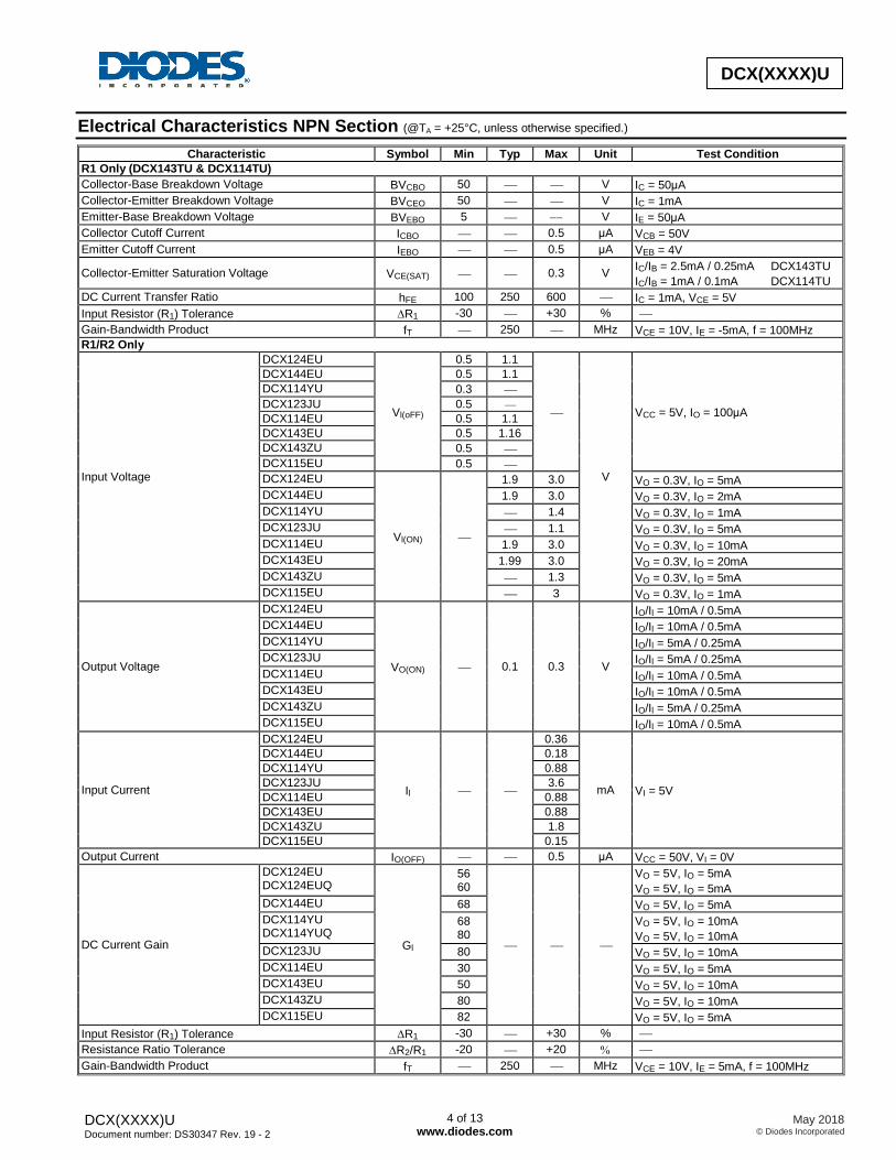
Electrical Characteristics NPN Section (@TA = +25°C, unless otherwise specified.)
Characteristic Symbol Min Typ Max Unit Test Condition
R1 Only (DCX143TU & DCX114TU)
Collector-Base Breakdown Voltage BVCBO 50 V IC = 50μA
Collector-Emitter Breakdown Voltage BVCEO 50 V IC = 1mA
Emitter-Base Breakdown Voltage BVEBO 5 V IE = 50μA
Collector Cutoff Current ICBO 0.5 μA VCB = 50V
Emitter Cutoff Current IEBO 0.5 μA VEB = 4V
Collector-Emitter Saturation Voltage VCE(SAT) 0.3 V IC/IB = 2.5mA / 0.25mA DCX143TU
IC/IB = 1mA / 0.1mA DCX114TU
DC Current Transfer Ratio hFE 100 250 600 IC = 1mA, VCE = 5V
Input Resistor (R1) Tolerance R1 -30 +30 %
Gain-Bandwidth Product fT 250 MHz VCE = 10V, IE = -5mA, f = 100MHz
R1/R2 Only
Input Voltage
DCX124EU
Vl(oFF)
0.5 1.1
V
VCC = 5V, IO = 100μA
DCX144EU 0.5 1.1
DCX114YU 0.3
DCX123JU 0.5
DCX114EU 0.5 1.1
DCX143EU 0.5 1.16
DCX143ZU 0.5
DCX115EU 0.5
DCX124EU
Vl(ON)
1.9 3.0 VO = 0.3V, IO = 5mA
DCX144EU 1.9 3.0 VO = 0.3V, IO = 2mA
DCX114YU 1.4 VO = 0.3V, IO = 1mA
DCX123JU 1.1 VO = 0.3V, IO = 5mA
DCX114EU 1.9 3.0 VO = 0.3V, IO = 10mA
DCX143EU 1.99 3.0 VO = 0.3V, IO = 20mA
DCX143ZU 1.3 VO = 0.3V, IO = 5mA
DCX115EU 3 VO = 0.3V, IO = 1mA
Output Voltage
DCX124EU
VO(ON) 0.1 0.3 V
IO/Il = 10mA / 0.5mA
DCX144EU IO/Il = 10mA / 0.5mA
DCX114YU IO/Il = 5mA / 0.25mA
DCX123JU IO/Il = 5mA / 0.25mA
DCX114EU IO/Il = 10mA / 0.5mA
DCX143EU IO/Il = 10mA / 0.5mA
DCX143ZU IO/Il = 5mA / 0.25mA
DCX115EU IO/Il = 10mA / 0.5mA
Input Current
DCX124EU
Il
0.36
mA VI = 5V
DCX144EU 0.18
DCX114YU 0.88
DCX123JU 3.6
DCX114EU 0.88
DCX143EU 0.88
DCX143ZU 1.8
DCX115EU 0.15
Output Current IO(OFF) 0.5 μA VCC = 50V, VI = 0V
DC Current Gain
DCX124EU DCX124EUQ
Gl
56 60
VO = 5V, IO = 5mA
VO = 5V, IO = 5mA
DCX144EU 68 VO = 5V, IO = 5mA
DCX114YU DCX114YUQ
68 80
VO = 5V, IO = 10mA
VO = 5V, IO = 10mA
DCX123JU 80 VO = 5V, IO = 10mA
DCX114EU 30 VO = 5V, IO = 5mA
DCX143EU 50 VO = 5V, IO = 10mA
DCX143ZU 80 VO = 5V, IO = 10mA
DCX115EU 82 VO = 5V, IO = 5mA
Input Resistor (R1) Tolerance R1 -30 +30 %
Resistance Ratio Tolerance R2/R1 -20 +20
Gain-Bandwidth Product fT 250 MHz VCE = 10V, IE = 5mA, f = 100MHz
DCX(XXXX)U Document number: DS30347 Rev. 19 - 2
5 of 13 www.diodes.com
May 2018 © Diodes Incorporated
DCX(XXXX)U
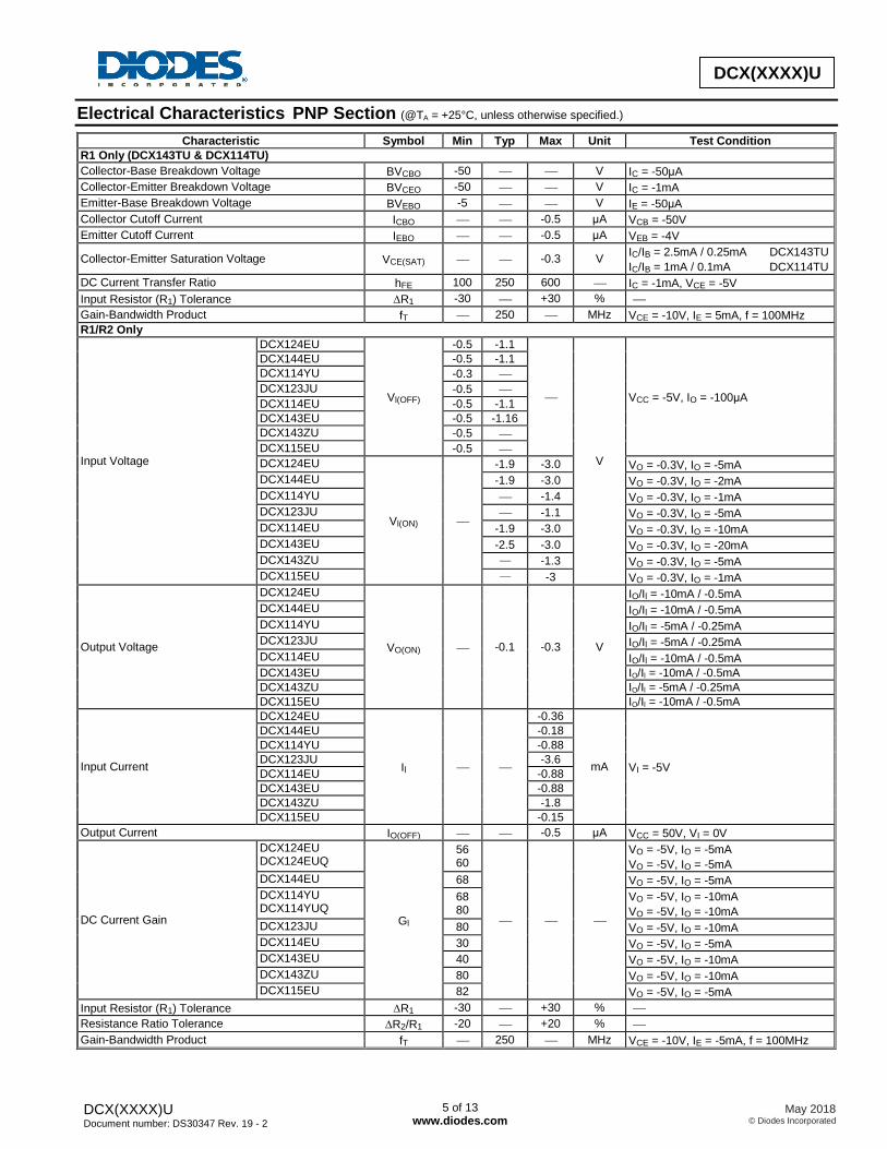
Electrical Characteristics PNP Section (@TA = +25°C, unless otherwise specified.)
Characteristic Symbol Min Typ Max Unit Test Condition
R1 Only (DCX143TU & DCX114TU)
Collector-Base Breakdown Voltage BVCBO -50 V IC = -50μA
Collector-Emitter Breakdown Voltage BVCEO -50 V IC = -1mA
Emitter-Base Breakdown Voltage BVEBO -5 V IE = -50μA
Collector Cutoff Current ICBO -0.5 μA VCB = -50V
Emitter Cutoff Current IEBO -0.5 μA VEB = -4V
Collector-Emitter Saturation Voltage VCE(SAT) -0.3 V IC/IB = 2.5mA / 0.25mA DCX143TU
IC/IB = 1mA / 0.1mA DCX114TU
DC Current Transfer Ratio hFE 100 250 600 IC = -1mA, VCE = -5V
Input Resistor (R1) Tolerance R1 -30 +30 %
Gain-Bandwidth Product fT 250 MHz VCE = -10V, IE = 5mA, f = 100MHz
R1/R2 Only
Input Voltage
DCX124EU
Vl(OFF)
-0.5 -1.1
V
VCC = -5V, IO = -100μA
DCX144EU -0.5 -1.1
DCX114YU -0.3
DCX123JU -0.5
DCX114EU -0.5 -1.1
DCX143EU -0.5 -1.16
DCX143ZU -0.5
DCX115EU -0.5
DCX124EU
Vl(ON)
-1.9 -3.0 VO = -0.3V, IO = -5mA
DCX144EU -1.9 -3.0 VO = -0.3V, IO = -2mA
DCX114YU -1.4 VO = -0.3V, IO = -1mA
DCX123JU -1.1 VO = -0.3V, IO = -5mA
DCX114EU -1.9 -3.0 VO = -0.3V, IO = -10mA
DCX143EU -2.5 -3.0 VO = -0.3V, IO = -20mA
DCX143ZU -1.3 VO = -0.3V, IO = -5mA
DCX115EU -3 VO = -0.3V, IO = -1mA
Output Voltage
DCX124EU
VO(ON) -0.1 -0.3 V
IO/Il = -10mA / -0.5mA
DCX144EU IO/Il = -10mA / -0.5mA
DCX114YU IO/Il = -5mA / -0.25mA
DCX123JU IO/Il = -5mA / -0.25mA
DCX114EU IO/Il = -10mA / -0.5mA
DCX143EU IO/Il = -10mA / -0.5mA
DCX143ZU IO/Il = -5mA / -0.25mA
DCX115EU IO/Il = -10mA / -0.5mA
Input Current
DCX124EU
Il
-0.36
mA VI = -5V
DCX144EU -0.18
DCX114YU -0.88
DCX123JU -3.6
DCX114EU -0.88
DCX143EU -0.88
DCX143ZU -1.8
DCX115EU -0.15
Output Current IO(OFF) -0.5 μA VCC = 50V, VI = 0V
DC Current Gain
DCX124EU DCX124EUQ
Gl
56 60
VO = -5V, IO = -5mA
VO = -5V, IO = -5mA
DCX144EU 68 VO = -5V, IO = -5mA
DCX114YU DCX114YUQ
68 80
VO = -5V, IO = -10mA
VO = -5V, IO = -10mA
DCX123JU 80 VO = -5V, IO = -10mA
DCX114EU 30 VO = -5V, IO = -5mA
DCX143EU 40 VO = -5V, IO = -10mA
DCX143ZU 80 VO = -5V, IO = -10mA
DCX115EU 82 VO = -5V, IO = -5mA
Input Resistor (R1) Tolerance R1 -30 +30 %
Resistance Ratio Tolerance R2/R1 -20 +20 %
Gain-Bandwidth Product fT 250 MHz VCE = -10V, IE = -5mA, f = 100MHz
DCX(XXXX)U Document number: DS30347 Rev. 19 - 2
6 of 13 www.diodes.com
May 2018 © Diodes Incorporated
DCX(XXXX)U
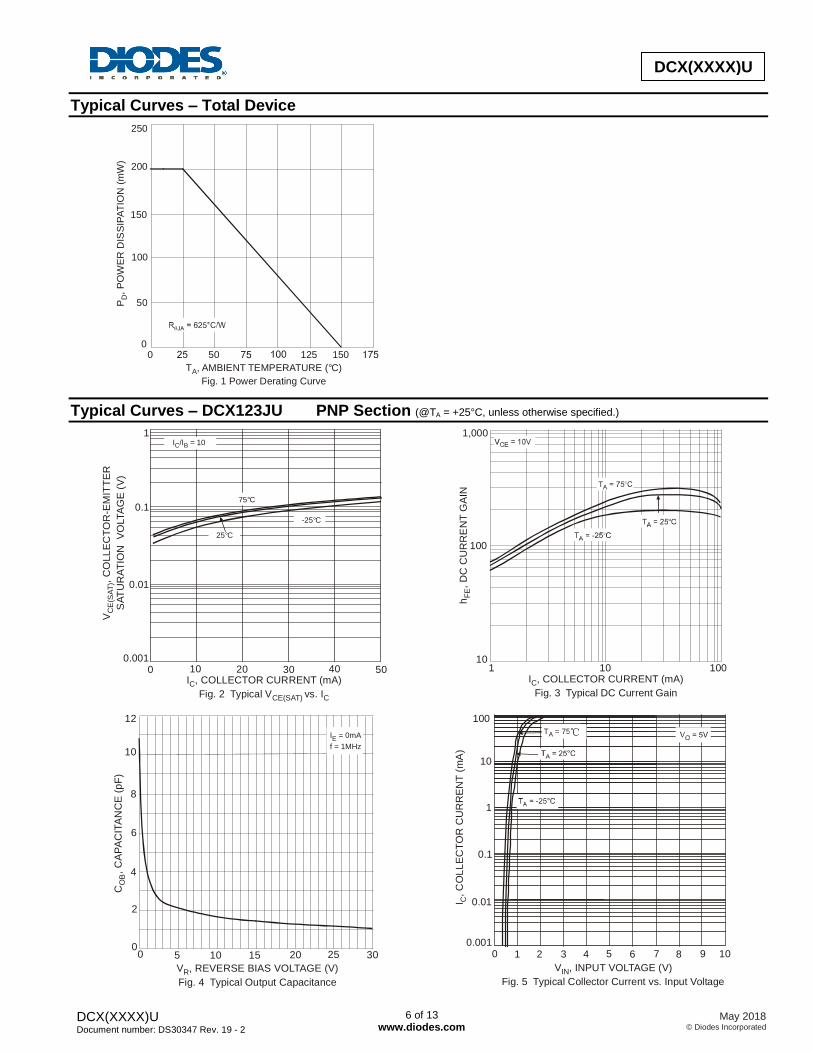
Typical Curves – Total Device
Typical Curves – DCX123JU PNP Section (@TA = +25°C, unless otherwise specified.)
0 50 125 150
250
200
150
50
100
0
T , AMBIENT TEMPERATURE ( C)
Fig. 1 Power Derating CurveA °
P,
PO
WE
R D
ISS
IPA
TIO
N (
mW
)D
0.001
0.01
0.1
1
0 10 20 30 40 50
V,
CO
LL
EC
TO
R-E
MIT
TE
R
SA
TU
RA
TIO
N
VO
LTA
GE
(V
)C
E(S
AT
)
I , COLLECTOR CURRENT (mA)
Fig. 2 Typical V vs. I C
CE(SAT) C
I /I = 10C B
-25 C°
75 C°
25 C°
10
1,000
100
1 10 100
h,
DC
CU
RR
EN
T G
AIN
FE
I , COLLECTOR CURRENT (mA)
Fig. 3 Typical DC Current GainC
0
2
4
6
12
0 20 30
C,
CA
PA
CIT
AN
CE
(p
F)
OB
V , REVERSE BIAS VOLTAGE (V)
Fig. 4 Typical Output CapacitanceR
105 15 25
8
10
I = 0mA
f = 1MHzE
0.001
0.01
1
10
100
0 1 2 3 4 8 9 10
I, C
OL
LE
CT
OR
CU
RR
EN
T (
mA
)C
V , INPUT VOLTAGE (V)
Fig. 5 Typical Collector Current vs. Input VoltageIN
5 6 7
0.1
T = 75癈A
DCX(XXXX)U Document number: DS30347 Rev. 19 - 2
7 of 13 www.diodes.com
May 2018 © Diodes Incorporated
DCX(XXXX)U
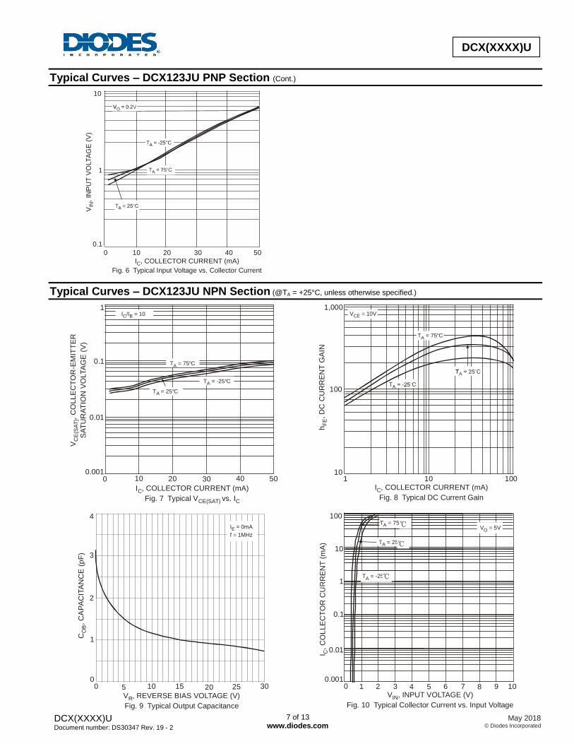
Typical Curves – DCX123JU PNP Section (Cont.)
Typical Curves – DCX123JU NPN Section (@TA = +25°C, unless otherwise specified.)
0.1
1
10
0 10 20 30 40 50
I , COLLECTOR CURRENT (mA)
Fig. 6 Typical Input Voltage vs. Collector CurrentC
V,
INP
UT
VO
LTA
GE
(V
)IN
0.001
0.01
0.1
1
0 10 20 30 40 50
V,
CO
LL
EC
TO
R-E
MIT
TE
R
SA
TU
RA
TIO
N V
OLTA
GE
(V
)C
E(S
AT
)
I , COLLECTOR CURRENT (mA)
Fig. 7 Typical V vs. I C
CE(SAT) C
I /I = 10C B
T = -25 CA °
T = 75 CA °
T = 25 CA °
10
1,000
100
1 10 100
h, D
C C
UR
RE
NT
GA
INF
E
I , COLLECTOR CURRENT (mA)
Fig. 8 Typical DC Current GainC
V = 10VCE
T = 75 CA °
0
1
2
3
4
0 20 30
C, C
AP
AC
ITA
NC
E (
pF
)O
B
V , REVERSE BIAS VOLTAGE (V)
Fig. 9 Typical Output CapacitanceR
105 15 25
I = 0mA
f = 1MHzE
0.001
0.01
1
10
100
0 1 2 3 4 8 9 10
I,
CO
LLE
CT
OR
CU
RR
EN
T (
mA
)C
V , INPUT VOLTAGE (V)
Fig. 10 Typical Collector Current vs. Input VoltageIN
T = -25癈A
5 6 7
T = 25癈A
0.1
V = 5VO
T = 75癈A

DCX(XXXX)U Document number: DS30347 Rev. 19 - 2
8 of 13 www.diodes.com
May 2018 © Diodes Incorporated
DCX(XXXX)U
Typical Curves – DCX123JU NPN Section (Cont.)
Typical Curves – DCX143EU PNP Section (@TA = +25°C, unless otherwise specified.)
0.1
1
10
0 10 20 30 40 50I , COLLECTOR CURRENT (mA)
Fig. 11 Typical Input Voltage vs. Collector CurrentC
V,
INP
UT
VO
LTA
GE
(V
)IN
I, C
OL
LE
CT
OR
CU
RR
EN
T (
A)
C
V , COLLECTOR EMITTER VOLTAGE (V)
Fig. 12 Typical V vs. ICE
CE C
I = 0.5mAb
I = 1mAb
I = 4.5mAb
I = 3.5mAb
I = 3mAb
I = 2.5mAb
I = 1.5mAb
I = 2mAb
I = 4mAbh
, D
C C
UR
RE
NT
GA
INF
E
I , COLLECTOR CURRENT (mA)
Fig. 13 Typical DC Current GainC
V, C
OL
LE
CT
OR
-EM
ITT
ER
SA
TU
RA
TIO
N V
OLTA
GE
(V
)C
E(S
AT
)
I , COLLECTOR CURRENT (mA)
Fig. 14 Typical V vs. IC
CE(SAT) C
I /I = 10C B
V,
BA
SE
-EM
ITT
ER
VO
LTA
GE
(V
)B
E
I , COLLECTOR CURRENT (mA)
Fig. 15 Typical V vs. IC
BE C

DCX(XXXX)U Document number: DS30347 Rev. 19 - 2
9 of 13 www.diodes.com
May 2018 © Diodes Incorporated
DCX(XXXX)U
Typical Curves – DCX143EU PNP Section (Cont.)
Typical Curves – DCX143EU NPN Section (@TA = +25°C, unless otherwise specified.)
V,
BA
SE
-EM
ITT
ER
SA
TU
RA
TIO
N V
OLTA
GE
(V
)B
E(S
AT
)
I , COLLECTOR CURRENT (mA)
Fig. 16 Typical V vs. IC
BE(SAT) C
V, IN
PU
T V
OLTA
GE
(V
)I(
ON
)
I , OUTPUT CURRENT (mA)
Fig. 17 Typical V vs. IC
I(ON) C
I,
CO
LL
EC
TO
R C
UR
RE
NT
(A
)C
V , COLLECTOR EMITTER VOLTAGE (V)
Fig. 18 Typical V vs. ICE
CE C
h,
DC
CU
RR
EN
T G
AIN
FE
I , COLLECTOR CURRENT (mA)
Fig. 19 Typical DC Current GainC
V, C
OL
LE
CT
OR
-EM
ITT
ER
SA
TU
RA
TIO
N V
OLTA
GE
(V
)C
E(S
AT
)
I , COLLECTOR CURRENT (mA)
Fig. 20 Typical V vs. IC
CE(SAT) C
V, B
AS
E-E
MIT
TE
R V
OLTA
GE
(V
)B
E
I , COLLECTOR CURRENT (mA)
Fig. 21 Typical V vs. IC
BE C
DCX(XXXX)U Document number: DS30347 Rev. 19 - 2
10 of 13 www.diodes.com
May 2018 © Diodes Incorporated
DCX(XXXX)U
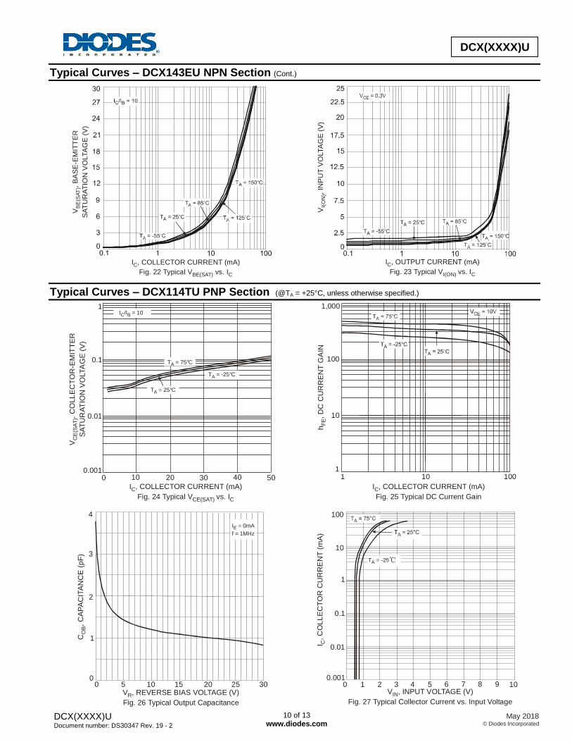
Typical Curves – DCX143EU NPN Section (Cont.)
Typical Curves – DCX114TU PNP Section (@TA = +25°C, unless otherwise specified.)
V,
BA
SE
-EM
ITT
ER
SA
TU
RA
TIO
N V
OLTA
GE
(V
)B
E(S
AT
)
I , COLLECTOR CURRENT (mA)
Fig. 22 Typical V vs. IC
BE(SAT) C
V,
INP
UT
VO
LTA
GE
(V
)I(
ON
)
I , OUTPUT CURRENT (mA)
Fig. 23 Typical V vs. IC
I(ON) C
0.001
0.01
0.1
1
0 10 20 30 40 50
V,
CO
LL
EC
TO
R-E
MIT
TE
R
SA
TU
RA
TIO
N V
OLTA
GE
(V
)C
E(S
AT
)
I , COLLECTOR CURRENT (mA)
Fig. 24 Typical V vs. I C
CE(SAT) C
I /I = 10C B
T = -25 CA °
T = 75 CA °
T = 25 CA °
10
1,000
100
11 10 100
h, D
C C
UR
RE
NT
GA
INF
E
I , COLLECTOR CURRENT (mA)
Fig. 25 Typical DC Current GainC
0
1
3
4
0 20 30
C,
CA
PA
CIT
AN
CE
(p
F)
OB
V , REVERSE BIAS VOLTAGE (V)
Fig. 26 Typical Output CapacitanceR
105 15 25
I = 0mA
f = 1MHzE
2
0.01
0.1
1
10
100
0 1 2 3 4 8 9 10
I, C
OL
LE
CT
OR
CU
RR
EN
T (
mA
)C
V , INPUT VOLTAGE (V)
Fig. 27 Typical Collector Current vs. Input VoltageIN
T = -25癈A
5 6 70.001

DCX(XXXX)U Document number: DS30347 Rev. 19 - 2
11 of 13 www.diodes.com
May 2018 © Diodes Incorporated
DCX(XXXX)U
Typical Curves – DCX114TU PNP Section (Cont.)
Typical Curves – DCX114TU NPN Section (@TA = +25°C, unless otherwise specified.)
0.1
1
10
0 10 20 30 40 50
I , COLLECTOR CURRENT (mA)
Fig. 28 Typical Input Voltage vs. Collector CurrentC
V,
INP
UT
VO
LTA
GE
(V
)IN
0.001
0.01
0.1
1
0 10 20 30 40 50
V,
CO
LL
EC
TO
R-E
MIT
TE
R
SA
TU
RA
TIO
N V
OLTA
GE
(V
)C
E(S
AT
)
I , COLLECTOR CURRENT (mA)
Fig. 29 Typical V vs. I C
CE(SAT) C
I /I = 10C B
T = -25 CA °
T = 75 CA °
T = 25 CA °
10
1,000
100
11 10 100
h, D
C C
UR
RE
NT
GA
INF
E
I , COLLECTOR CURRENT (mA)
Fig. 30 Typical DC Current GainC
0
1
2
3
4
0 20 30
C,
CA
PA
CIT
AN
CE
(p
F)
OB
V , REVERSE BIAS VOLTAGE (V)
Fig. 31 Typical Output CapacitanceR
105 15 25
I = 0mA
f = 1MHzE
0.01
0.1
1
10
100
0 1 2 3 4 8 9 10
I, C
OLL
EC
TO
R C
UR
RE
NT
(m
A)
C
V , INPUT VOLTAGE (V)
Fig. 32 Typical Collector Current vs. Input VoltageIN
T =-25癈A
5 6 7
T = 75癈A
T = 25癈A
0.001

DCX(XXXX)U Document number: DS30347 Rev. 19 - 2
12 of 13 www.diodes.com
May 2018 © Diodes Incorporated
DCX(XXXX)U
Typical Curves – DCX114TU NPN Section (Cont.)
Package Outline Dimensions Please see http://www.diodes.com/package-outlines.html for the latest version.
SOT363
SOT363
Dim Min Max Typ
A1 0.00 0.10 0.05
A2 0.90 1.00 0.95
b 0.10 0.30 0.25
c 0.10 0.22 0.11
D 1.80 2.20 2.15
E 2.00 2.20 2.10
E1 1.15 1.35 1.30
e 0.650 BSC
F 0.40 0.45 0.425
L 0.25 0.40 0.30
a 0° 8° --
All Dimensions in mm
0.1
1
10
0 10 20 30 40 50
I , COLLECTOR CURRENT (mA)
Fig. 33 Typical Input Voltage vs. Collector CurrentC
V, IN
PU
T V
OLTA
GE
(V
)IN
e
D
L
E1
b
E
F
A2
A1
c a
DCX(XXXX)U Document number: DS30347 Rev. 19 - 2
13 of 13 www.diodes.com
May 2018 © Diodes Incorporated
DCX(XXXX)U
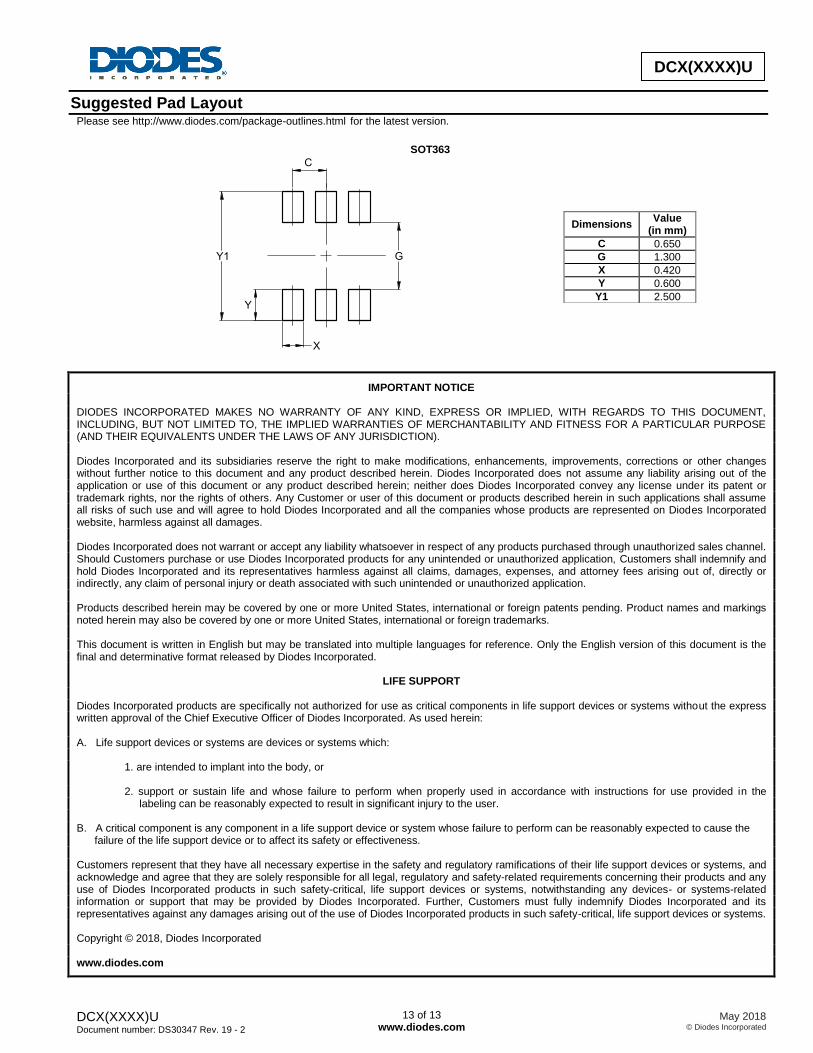
Suggested Pad Layout Please see http://www.diodes.com/package-outlines.html for the latest version.
SOT363
Dimensions Value
(in mm)
C 0.650
G 1.300
X 0.420
Y 0.600
Y1 2.500
IMPORTANT NOTICE DIODES INCORPORATED MAKES NO WARRANTY OF ANY KIND, EXPRESS OR IMPLIED, WITH REGARDS TO THIS DOCUMENT, INCLUDING, BUT NOT LIMITED TO, THE IMPLIED WARRANTIES OF MERCHANTABILITY AND FITNESS FOR A PARTICULAR PURPOSE (AND THEIR EQUIVALENTS UNDER THE LAWS OF ANY JURISDICTION). Diodes Incorporated and its subsidiaries reserve the right to make modifications, enhancements, improvements, corrections or other changes without further notice to this document and any product described herein. Diodes Incorporated does not assume any liability arising out of the application or use of this document or any product described herein; neither does Diodes Incorporated convey any license under its patent or trademark rights, nor the rights of others. Any Customer or user of this document or products described herein in such applications shall assume all risks of such use and will agree to hold Diodes Incorporated and all the companies whose products are represented on Diodes Incorporated website, harmless against all damages. Diodes Incorporated does not warrant or accept any liability whatsoever in respect of any products purchased through unauthorized sales channel. Should Customers purchase or use Diodes Incorporated products for any unintended or unauthorized application, Customers shall indemnify and hold Diodes Incorporated and its representatives harmless against all claims, damages, expenses, and attorney fees arising out of, directly or indirectly, any claim of personal injury or death associated with such unintended or unauthorized application. Products described herein may be covered by one or more United States, international or foreign patents pending. Product names and markings noted herein may also be covered by one or more United States, international or foreign trademarks. This document is written in English but may be translated into multiple languages for reference. Only the English version of this document is the final and determinative format released by Diodes Incorporated.
LIFE SUPPORT Diodes Incorporated products are specifically not authorized for use as critical components in life support devices or systems without the express written approval of the Chief Executive Officer of Diodes Incorporated. As used herein: A. Life support devices or systems are devices or systems which: 1. are intended to implant into the body, or
2. support or sustain life and whose failure to perform when properly used in accordance with instructions for use provided in the labeling can be reasonably expected to result in significant injury to the user.
B. A critical component is any component in a life support device or system whose failure to perform can be reasonably expected to cause the failure of the life support device or to affect its safety or effectiveness. Customers represent that they have all necessary expertise in the safety and regulatory ramifications of their life support devices or systems, and acknowledge and agree that they are solely responsible for all legal, regulatory and safety-related requirements concerning their products and any use of Diodes Incorporated products in such safety-critical, life support devices or systems, notwithstanding any devices- or systems-related information or support that may be provided by Diodes Incorporated. Further, Customers must fully indemnify Diodes Incorporated and its representatives against any damages arising out of the use of Diodes Incorporated products in such safety-critical, life support devices or systems. Copyright © 2018, Diodes Incorporated www.diodes.com
Y1 G
Y
X
C