
Infographics 101 for elearning (instructional designers + graphics designers)
Upload
phamkhuongCategory
view
213download
0
Features BlueCore® CSR8635 QFN Bluetooth® v4.0 specification compliant 80MHz RISC MCU and 80MIPS Kalimba DSP Stereo codec with 1 microphone input Internal ROM, serial flash memory and EEPROM
interfaces High-performance Stereo codec Radio includes integrated balun with RF
performance of 8dBm transmit power and -89dBmreceiver sensitivity
AVRCP v1.4 5-band fully configurable EQ Wideband speech supported by HFP v1.6 and
mSBC codec CSR's latest CVC technology for narrowband and
wideband voice connections including wind noisereduction
Multipoint support for A2DP connection to 2A2DP sources for music playback
Secure simple pairing, CSR's proximity pairing andCSR's proximity connections
Stereo line-in Serial interfaces: USB 2.0, UART, I²C and SPI SBC, MP3 and AAC decoder support Wired audio support Integrated dual switch-mode regulators, linear
regulators and battery charger External crystal load capacitors not required for
typical crystals 3 LED outputs (RGB) 68-lead QFN 8 x 8 x 0.9mm 0.4mm pitch Green (RoHS compliant and no antimony or
halogenated flame retardants)
CSR8635 Stereo ROM Solution
1-mic CVC Audio Enhancement
Fully Qualified Single-chipBluetooth® v4.0 System
Production Information
CSR8635A04
Issue 5
2.4GHz Radio
+Balun
I /OBT_RF
RAM
Baseband
MCU
Kalimba DSP
ROMXTALSerial Flash /
EEPROM
UART/USB
Audio In /Out
Debug SPI
PIO
SPI/ I2C
General DescriptionCSR's BlueCore® CSR8635 QFN is a single-chipBluetooth ROM audio solution for rapid evaluation anddevelopment of Bluetooth ROM stereo applications.BlueCore® CSR8635 QFN consumer audio platform forwired and wireless applications using the QFN packageintegrates an ultra-low power DSP and applicationprocessor with embedded flash memory, a high-performance stereo codec, a power managementsubsystem and LED drivers.The CSR configuration tools and the development kitprovide a flexible and powerful development platform todesign advanced and high-quality Bluetooth stereoproducts using BlueCore® CSR8635 QFN single-chipBluetooth audio solution.
Applications Stereo speakers Speakerphones 1-mic stereo headset or headphones Handsfree car kitsThe enhanced Kalimba DSP coprocessor with 80MIPSsupports enhanced audio and DSP applications.The integrated audio codec supports stereo input andoutput, as well as a variety of audio standards.See CSR Glossary at www.csrsupport.com.
Production Information© Cambridge Silicon Radio Limited 2013Confidential Information - This Material is Subject to CSR's Non-disclosure Agreement
Page 1 of 105CS-303725-DSP5
www.csr.com
CSR
8635 QFN D
ata Sheet
Prepa
red
for q
ingbo
keve
n.zh
ou -
exce
lpoint
.com
.cn -
Friday
, Sep
tem
ber 2
7, 2
013

Ordering Information
Device
Package
Order NumberType Size Shipment
Method
CSR8635 StereoROM Solution
QFN‑68-lead(Pb free)
8 x 8 x 0.9mm0.4mm pitch
Tape and reel CSR8635A04‑IQQF‑R
Note:
CSR8635 QFN is a ROM-based device where the product code has the form CSR8635Axx. Axx is the specificROM-variant, A04 is the ROM-variant for CSR8635 Stereo ROM Solution.
Minimum order quantity is 2kpcs taped and reeled.
Supply chain: CSR's manufacturing policy is to multisource volume products. For further details, contact your localsales account manager or representative.
Contacts
General informationInformation on this productCustomer support for this productDetails of compliance and standardsHelp with this document
[email protected]@[email protected]
CSR8635 Stereo ROM Solution Development Kit Ordering Information
Description Order Number
CSR8635 Stereo ROM Solution Audio Development Kit DK‑8635‑10163‑1A
Production Information© Cambridge Silicon Radio Limited 2013Confidential Information - This Material is Subject to CSR's Non-disclosure Agreement
Page 2 of 105CS-303725-DSP5
www.csr.com
CSR
8635 QFN D
ata Sheet
Prepa
red
for q
ingbo
keve
n.zh
ou -
exce
lpoint
.com
.cn -
Friday
, Sep
tem
ber 2
7, 2
013

Device DetailsBluetooth low energy Dual-mode Bluetooth low energy radio Support for Bluetooth basic rate / EDR and low
energy connections 3 Bluetooth low energy connections at the same time
as basic rate A2DPBluetooth Radio On-chip balun (50Ω impedance) No production trimming of external components Bluetooth v4.0 specification compliantBluetooth Transmitter 8dBm (typ) RF transmit power with level control Class 1, Class 2 and Class 3 support, no external
PA or TX/RX switch requiredBluetooth Receiver -91dBm (typ) π/4 DQPSK receiver sensitivity and
-81dBm (typ) 8DPSK receiver sensitivity Integrated channel filters Digital demodulator for improved sensitivity and co-
channel rejection Real-time digitised RSSI available to application Fast AGC for enhanced dynamic range Channel classification for AFHBluetooth Synthesiser Fully integrated synthesiser requires no external
VCO, varactor diode, resonator or loop filter Compatible with crystals 16MHz to 32MHzKalimba DSP Enhanced Kalimba DSP coprocessor, 80MIPS,
24‑bit fixed point core 2 single-cycle MACs; 24 x 24-bit multiply and 56-bit
accumulator 32-bit instruction word, dual 24-bit data memory 6K x 32-bit program RAM including 1K instruction
cache for executing out of internal ROM 16K x 24-bit + 16K x 24-bit 2-bank data RAMAudio Interfaces Stereo audio ADC with line input Stereo audio DAC Supported sample rates of 8, 11.025, 16, 22.05, 32,
44.1, 48 and 96kHz (DAC only)Auxiliary Features Crystal oscillator with built-in digital trimmingPackage Option 68-lead QFN 8 x 8 x 0.9mm 0.4mm pitch
Physical Interfaces UART interface for debug USB 2.0 (full-speed) interface, including charger
enumeration 1-bit SPI flash memory interface SPI interface for debug and programming I²C interface for EEPROM Up to 22 general purpose PIOs with 3 extra open-
drain PIOs available when LED not used PCM and I²S (only in HCI mode) interfaces 3 LED drivers (includes RGB) with PWM flasher
independent of MCUIntegrated Power Control and Regulation Automatic power switching to charger when present 2 high-efficiency switch-mode regulators with 1.8V
and 1.35V outputs direct from battery supply 3.3V linear regulator for USB supply Low-voltage linear regulator for internal digital circuits Low-voltage linear regulator for internal analogue
circuits Power-on-reset detects low supply voltage Power management includes digital shutdown and
wake-up commands for ultra-low power modesBattery Charger Lithium ion / Lithium polymer battery charger Instant-on function automatically selects the power
supply between battery and USB, which enablesoperation even if the battery is fully discharged
Fast charging support up to 200mA with no externalcomponents. Higher charge currents using externalpass device.
Supports USB charger detection Support for thermistor protection of battery pack Support to enable end product design to PSE law:
Design to JIS-C 8712/8714 (batteries) Testing based on IEEE 1725
Baseband and Software Internal ROM Memory protection unit supporting accelerated VM 56KB internal RAM, enables full-speed data transfer,
and full piconet support Logic for forward error correction, header error
control, access code correlation, CRC,demodulation, encryption bit stream generation,whitening and transmit pulse shaping
Production Information© Cambridge Silicon Radio Limited 2013Confidential Information - This Material is Subject to CSR's Non-disclosure Agreement
Page 3 of 105CS-303725-DSP5
www.csr.com
CSR
8635 QFN D
ata Sheet
Prepa
red
for q
ingbo
keve
n.zh
ou -
exce
lpoint
.com
.cn -
Friday
, Sep
tem
ber 2
7, 2
013

CSR8635 Stereo ROM Solution DetailsBluetooth Profiles Bluetooth v4.0 specification support A2DP v1.2 AVRCP v1.4 HFP v1.6 HSP v1.2 DI v1.3Music Enhancements Configurable 5-band EQ for music playback (rock,
pop, classical, jazz, dance etc) SBC, MP3, AAC and Faststream decoder Volume Boost Stereo Widening (S3D)Additional Functionality Support for multi-language programmable audio
prompts CSR's proximity pairing and CSR's proximity
connection Multipoint support for A2DP connection to 2 A2DP
sources for music playback Talk-time extensionCSR8600 ROM Series Configuration ToolConfigures the CSR8635 stereo ROM solution softwarefeatures: Bluetooth v4.0 specification features Reconnection policies, e.g. reconnect on power-on Audio features, including default volumes Button events: configuring button presses and
durations for certain events, e.g. double press onPIO for last number redial
LED indications for states, e.g. device connected,and events, e.g. power on
Indication tones for events and ringtones Battery divider ratios and thresholds, e.g. thresholds
for battery low indication, full battery etc. Advanced Multipoint settings
CSR8635 Stereo ROM Solution Development Kit Example CSR8635 QFN module design Carrier board Output stage: headphone amplifier Interface adapters and cables Works in conjunction with the CSR8600 ROM Series
Configuration Tool and other supporting utilities
Production Information© Cambridge Silicon Radio Limited 2013Confidential Information - This Material is Subject to CSR's Non-disclosure Agreement
Page 4 of 105CS-303725-DSP5
www.csr.com
CSR
8635 QFN D
ata Sheet
Prepa
red
for q
ingbo
keve
n.zh
ou -
exce
lpoint
.com
.cn -
Friday
, Sep
tem
ber 2
7, 2
013

Functional Block Diagram
G-T
W-0
0129
58.3
.2
Memory Management
Unit
Bluetooth Modem
80MHz DSP
I2C/SPIMaster/Slave
SPI(Debug)
UART4Mbps
SystemRAM
Serial Flash Interface
DMA ports
DM
A po
rts
PCM1 / I2S
ROM
SPI_DEBUG Serial FlashI2C
LINE/MIC_AN
UART
80MHz MCU
SPKR_LN
AudioInterface
MIC_BIAS
USB v2.0 Full-speed
USB
3.3V
MIC Bias
VM Accelerator(MPU)
PMUInterface
andBIST
Engine
LED PWMControl and
Output
PM
DM1
DM2
R G B
Digital Audio
1.35VSwitch-mode
Regulator
BypassLDO
LXL_1V8
Li-ion Charger
VCHG
1.8VSwitch-mode
Regulator
LX_1V35
SMPS_1V8_SE
NS
E
3V3_USB
Voltage / Temperature Monitor
BT_RF
ClockGeneration AUX ADC
XTAL AIO[0]
LINE/MIC_AP
LINE_BNLINE_BP
SPKR_LP
SPKR_RNSPKR_RP
SENSE SENSE
Bluetooth Baseband
Bluetooth Radioand Balun
TX
RX
High-quality ADC
High-quality ADC
High-quality DAC
High-quality DAC
1.35VLow-voltage VDD_AUX
Linear Regulator
1.35VLow-voltage VDD_ANA
Linear Regulator
0.85V to 1.2V
Low-voltage VDD_DIG
Linear Regulator
DM
A po
rts
VDD
_AUX
SENSE
VDD
_ANA
SENSE
VDD
_DIG
SENSE
CHG_EXT
Switch
SMPS_1V35_SE
NSE
SENSE
VBAT
VDD
_AUX_1V8
VREG
IN_D
IG
PIO Port
PIO
PIO Port
VBAT_SENSE
VDD_AUDIO
VDD_AUDIO_DRV
VDD
_BT_RAD
IO
Production Information© Cambridge Silicon Radio Limited 2013Confidential Information - This Material is Subject to CSR's Non-disclosure Agreement
Page 5 of 105CS-303725-DSP5
www.csr.com
CSR
8635 QFN D
ata Sheet
Prepa
red
for q
ingbo
keve
n.zh
ou -
exce
lpoint
.com
.cn -
Friday
, Sep
tem
ber 2
7, 2
013

Document HistoryRevision Date Change Reason
1 19 JUL 13 Original publication of this document.
2 20 AUG 13 Updates include: Engineering Sample release added. RF specification. PCB design and assembly considerations. MIC_BN and MIC_BP to LINE_BN and LINE_BP. AVRCP v1.4 added. HFP and HSP profiles added. PCM interface for HCI only. Minor editorial updates.
3 13 SEP 13 Updates include: Pre-production Information added. Development kit information. Package dimensions. Example application schematic.
4 23 SEP 13 Updates include: Production Information added. Ordering information. RF specification. Package information. VDD_DIG_MEM signal name corrected to VDD_DIG. SPI_PCM#_SEL signal name corrected to SPI_PCM#. Example application schematic. Audio codec parameters. Power consumption.
5 24 SEP 13 Minor editorial updates.
Production Information© Cambridge Silicon Radio Limited 2013Confidential Information - This Material is Subject to CSR's Non-disclosure Agreement
Page 6 of 105CS-303725-DSP5
www.csr.com
CSR
8635 QFN D
ata Sheet
Prepa
red
for q
ingbo
keve
n.zh
ou -
exce
lpoint
.com
.cn -
Friday
, Sep
tem
ber 2
7, 2
013

Status InformationThe status of this Data Sheet is Production Information. CSR Product Data Sheets progress according to the following format: Advance Information:
Information for designers concerning CSR product in development. All values specified are the target values of the design.Minimum and maximum values specified are only given as guidance to the final specification limits and must not beconsidered as the final values.
Engineering Sample: Information about initial devices. Devices are untested or partially tested prototypes, their status is described in an
Engineering Sample Release Note. All values specified are the target values of the design. Minimum and maximum valuesspecified are only given as guidance to the final specification limits and must not be considered as the final values.
All detailed specifications including pinouts and electrical specifications may be changed by CSR without notice. Pre-production Information:
Pinout and mechanical dimension specifications finalised. All values specified are the target values of the design. Minimumand maximum values specified are only given as guidance to the final specification limits and must not be considered asthe final values.
All electrical specifications may be changed by CSR without notice. Production Information:
Final Data Sheet including the guaranteed minimum and maximum limits for the electrical specifications. Production Data Sheets supersede all previous document versions.
Device ImplementationImportant Note:
As the feature-set of the CSR8635 QFN is firmware build-specific, see the relevant software release note for the exactimplementation of features on the CSR8635 QFN.
Life Support Policy and Use in Safety-critical ApplicationsCSR's products are not authorised for use in life-support or safety-critical applications. Use in such applications is done at the solediscretion of the customer. CSR will not warrant the use of its devices in such applications. CSR Green Semiconductor Products and RoHS ComplianceCSR8635 QFN devices meet the requirements of Directive 2002/95/EC of the European Parliament and of the Council on theRestriction of Hazardous Substance (RoHS). CSR8635 QFN devices are free from halogenated or antimony trioxide-based flameretardants and other hazardous chemicals. For more information, see CSR's Environmental Compliance Statement for CSR GreenSemiconductor Products. Trademarks, Patents and LicencesUnless otherwise stated, words and logos marked with ™ or ® are trademarks registered or owned by CSR plc or its affiliates.Bluetooth ® and the Bluetooth ® logos are trademarks owned by Bluetooth ® SIG, Inc. and licensed to CSR. Other products, servicesand names used in this document may have been trademarked by their respective owners.The publication of this information does not imply that any license is granted under any patent or other rights owned by CSR plcand/or its affiliates.CSR reserves the right to make technical changes to its products as part of its development programme.While every care has been taken to ensure the accuracy of the contents of this document, CSR cannot accept responsibility for anyerrors.Refer to www.csrsupport.com for compliance and conformance to standards information.
Production Information© Cambridge Silicon Radio Limited 2013Confidential Information - This Material is Subject to CSR's Non-disclosure Agreement
Page 7 of 105CS-303725-DSP5
www.csr.com
CSR
8635 QFN D
ata Sheet
Prepa
red
for q
ingbo
keve
n.zh
ou -
exce
lpoint
.com
.cn -
Friday
, Sep
tem
ber 2
7, 2
013

ContentsOrdering Information ........................................................................................................................................... 2
Contacts ..................................................................................................................................................... 2CSR8635 Stereo ROM Solution Development Kit Ordering Information ................................................... 2
Device Details ..................................................................................................................................................... 3CSR8635 Stereo ROM Solution Details .............................................................................................................. 4Functional Block Diagram .................................................................................................................................. 5
1 Package Information ......................................................................................................................................... 131.1 Pinout Diagram ........................................................................................................................................ 131.2 Device Terminal Functions ....................................................................................................................... 141.3 Package Dimensions ............................................................................................................................... 201.4 PCB Design and Assembly Considerations ............................................................................................. 211.5 Typical Solder Reflow Profile ................................................................................................................... 21
2 Bluetooth Modem .............................................................................................................................................. 222.1 RF Ports ................................................................................................................................................... 22
2.1.1 BT_RF ........................................................................................................................................ 222.2 RF Receiver ............................................................................................................................................. 22
2.2.1 Low Noise Amplifier .................................................................................................................... 222.2.2 RSSI Analogue to Digital Converter ........................................................................................... 22
2.3 RF Transmitter ......................................................................................................................................... 222.3.1 IQ Modulator ............................................................................................................................... 222.3.2 Power Amplifier .......................................................................................................................... 23
2.4 Bluetooth Radio Synthesiser .................................................................................................................... 232.5 Baseband ................................................................................................................................................. 23
2.5.1 Burst Mode Controller ................................................................................................................. 232.5.2 Physical Layer Hardware Engine ............................................................................................... 23
3 Clock Generation ............................................................................................................................................... 243.1 Crystal ...................................................................................................................................................... 24
3.1.1 Negative Resistance Model ........................................................................................................ 253.1.2 Crystal Specification ................................................................................................................... 253.1.3 Crystal Calibration ...................................................................................................................... 25
3.2 Non-crystal Oscillator ............................................................................................................................... 263.2.1 XTAL_IN Impedance in Non-crystal Mode ................................................................................. 27
4 Bluetooth Stack Microcontroller ......................................................................................................................... 284.1 VM Accelerator ......................................................................................................................................... 28
5 Kalimba DSP ..................................................................................................................................................... 296 Memory Interface and Management ................................................................................................................. 30
6.1 Memory Management Unit ....................................................................................................................... 306.2 System RAM ............................................................................................................................................ 306.3 Kalimba DSP RAM ................................................................................................................................... 306.4 Internal ROM ............................................................................................................................................ 306.5 Serial Flash Interface ............................................................................................................................... 30
7 Serial Interfaces ................................................................................................................................................ 317.1 USB Interface ........................................................................................................................................... 317.2 UART Interface ........................................................................................................................................ 317.3 Programming and Debug Interface .......................................................................................................... 33
7.3.1 Multi-slave Operation .................................................................................................................. 337.4 I²C EEPROM Interface ............................................................................................................................. 34
8 Interfaces ........................................................................................................................................................... 358.1 Programmable I/O Ports, PIO .................................................................................................................. 35
Production Information© Cambridge Silicon Radio Limited 2013Confidential Information - This Material is Subject to CSR's Non-disclosure Agreement
Page 8 of 105CS-303725-DSP5
www.csr.com
CSR
8635 QFN D
ata Sheet
Prepa
red
for q
ingbo
keve
n.zh
ou -
exce
lpoint
.com
.cn -
Friday
, Sep
tem
ber 2
7, 2
013

8.2 Analogue I/O Ports, AIO ........................................................................................................................... 358.3 LED Drivers .............................................................................................................................................. 35
9 Audio Interface .................................................................................................................................................. 379.1 Audio Input and Output ............................................................................................................................ 379.2 Audio Codec Interface .............................................................................................................................. 38
9.2.1 Audio Codec Block Diagram ....................................................................................................... 389.2.2 ADC ............................................................................................................................................ 389.2.3 ADC Sample Rate Selection ...................................................................................................... 389.2.4 ADC Audio Input Gain ................................................................................................................ 399.2.5 ADC Pre-amplifier and ADC Analogue Gain .............................................................................. 399.2.6 ADC Digital Gain ........................................................................................................................ 399.2.7 ADC Digital IIR Filter .................................................................................................................. 409.2.8 DAC ............................................................................................................................................ 409.2.9 DAC Sample Rate Selection ...................................................................................................... 409.2.10 DAC Digital Gain ........................................................................................................................ 409.2.11 DAC Analogue Gain ................................................................................................................... 409.2.12 DAC Digital FIR Filter ................................................................................................................. 419.2.13 Microphone Input ........................................................................................................................ 419.2.14 Line Input .................................................................................................................................... 429.2.15 Output Stage .............................................................................................................................. 429.2.16 Mono Operation .......................................................................................................................... 439.2.17 Side Tone ................................................................................................................................... 439.2.18 Integrated Digital IIR Filter .......................................................................................................... 45
9.3 PCM1 Interface ........................................................................................................................................ 469.3.1 PCM Interface Master/Slave ....................................................................................................... 469.3.2 Long Frame Sync ....................................................................................................................... 479.3.3 Short Frame Sync ....................................................................................................................... 479.3.4 Multi-slot Operation .................................................................................................................... 489.3.5 GCI Interface .............................................................................................................................. 489.3.6 Slots and Sample Formats ......................................................................................................... 489.3.7 Additional Features ..................................................................................................................... 499.3.8 PCM Timing Information ............................................................................................................. 499.3.9 PCM_CLK and PCM_SYNC Generation .................................................................................... 539.3.10 PCM Configuration ..................................................................................................................... 53
9.4 Digital Audio Interface (I²S) ...................................................................................................................... 5310 Power Control and Regulation .......................................................................................................................... 57
10.1 1.8V Switch-mode Regulator ................................................................................................................... 5910.2 1.35V Switch-mode Regulator ................................................................................................................. 6010.3 1.8V and 1.35V Switch-mode Regulators Combined ............................................................................... 6110.4 Bypass LDO Linear Regulator ................................................................................................................. 6210.5 Low-voltage VDD_DIG Linear Regulator ................................................................................................. 6310.6 Low-voltage VDD_AUX Linear Regulator ................................................................................................ 6310.7 Low-voltage VDD_ANA Linear Regulator ................................................................................................ 6310.8 Voltage Regulator Enable ........................................................................................................................ 6310.9 External Regulators and Power Sequencing ........................................................................................... 6310.10Reset, RST# ............................................................................................................................................. 63
10.10.1 Digital Pin States on Reset ......................................................................................................... 6410.10.2 Status After Reset ...................................................................................................................... 64
10.11Automatic Reset Protection ...................................................................................................................... 6411 Battery Charger ................................................................................................................................................. 65
11.1 Battery Charger Hardware Operating Modes ........................................................................................... 6511.1.1 Disabled Mode ............................................................................................................................ 66
Production Information© Cambridge Silicon Radio Limited 2013Confidential Information - This Material is Subject to CSR's Non-disclosure Agreement
Page 9 of 105CS-303725-DSP5
www.csr.com
CSR
8635 QFN D
ata Sheet
Prepa
red
for q
ingbo
keve
n.zh
ou -
exce
lpoint
.com
.cn -
Friday
, Sep
tem
ber 2
7, 2
013

11.1.2 Trickle Charge Mode .................................................................................................................. 6611.1.3 Fast Charge Mode ...................................................................................................................... 6611.1.4 Standby Mode ............................................................................................................................ 6611.1.5 Error Mode .................................................................................................................................. 66
11.2 Battery Charger Trimming and Calibration ............................................................................................... 6611.3 VM Battery Charger Control ..................................................................................................................... 6611.4 Battery Charger Firmware and PS Keys .................................................................................................. 6611.5 External Mode .......................................................................................................................................... 67
12 Example Application Schematic ........................................................................................................................ 6813 Electrical Characteristics ................................................................................................................................... 70
13.1 Absolute Maximum Ratings ..................................................................................................................... 7013.2 Recommended Operating Conditions ...................................................................................................... 7113.3 Input/Output Terminal Characteristics ...................................................................................................... 72
13.3.1 Regulators: Available For External Use ...................................................................................... 7213.3.2 Regulators: For Internal Use Only .............................................................................................. 7413.3.3 Regulator Enable ........................................................................................................................ 7513.3.4 Battery Charger .......................................................................................................................... 7513.3.5 USB ............................................................................................................................................ 7713.3.6 Stereo Codec: Analogue to Digital Converter ............................................................................. 7813.3.7 Stereo Codec: Digital to Analogue Converter ............................................................................. 7913.3.8 Digital .......................................................................................................................................... 8013.3.9 LED Driver Pads ......................................................................................................................... 8013.3.10 Auxiliary ADC ............................................................................................................................. 8113.3.11 Auxiliary DAC ............................................................................................................................. 81
13.4 ESD Protection ......................................................................................................................................... 8213.4.1 USB Electrostatic Discharge Immunity ....................................................................................... 82
14 Power Consumption .......................................................................................................................................... 8415 CSR Green Semiconductor Products and RoHS Compliance .......................................................................... 8716 Software ............................................................................................................................................................ 88
16.1 CSR8635 Stereo ROM Solution ............................................................................................................... 8816.1.1 Advanced Multipoint Support ...................................................................................................... 8916.1.2 A2DP Multipoint Support ............................................................................................................ 8916.1.3 Wired Audio Mode ...................................................................................................................... 8916.1.4 USB Modes Including USB Audio Mode .................................................................................... 8916.1.5 Smartphone Applications (Apps) ................................................................................................ 9016.1.6 Programmable Audio Prompts ................................................................................................... 9016.1.7 CSR’s Intelligent Power Management ........................................................................................ 9116.1.8 Proximity Pairing ......................................................................................................................... 9116.1.9 Proximity Connection .................................................................................................................. 91
16.2 6th Generation 1-mic CVC ENR Technology for Hands-free and Audio Enhancements ......................... 9216.2.1 Acoustic Echo Cancellation ........................................................................................................ 9216.2.2 Noise Suppression with Wind Noise Reduction ......................................................................... 9316.2.3 Non-linear Processing (NLP) ...................................................................................................... 9316.2.4 Howling Control (HC) .................................................................................................................. 9316.2.5 Comfort Noise Generator ........................................................................................................... 9316.2.6 Equalisation ................................................................................................................................ 9316.2.7 Automatic Gain Control .............................................................................................................. 9316.2.8 Packet Loss Concealment .......................................................................................................... 9316.2.9 Adaptive Equalisation (AEQ) ...................................................................................................... 9416.2.10 Auxiliary Stream Mix ................................................................................................................... 9416.2.11 Clipper ........................................................................................................................................ 9416.2.12 Noise Dependent Volume Control .............................................................................................. 94
Production Information© Cambridge Silicon Radio Limited 2013Confidential Information - This Material is Subject to CSR's Non-disclosure Agreement
Page 10 of 105CS-303725-DSP5
www.csr.com
CSR
8635 QFN D
ata Sheet
Prepa
red
for q
ingbo
keve
n.zh
ou -
exce
lpoint
.com
.cn -
Friday
, Sep
tem
ber 2
7, 2
013

16.2.13 Input Output Gains ..................................................................................................................... 9416.3 Music Enhancements ............................................................................................................................... 95
16.3.1 Audio Decoders .......................................................................................................................... 9516.3.2 Configurable EQ ......................................................................................................................... 9516.3.3 Stereo Widening (S3D) ............................................................................................................... 9516.3.4 Volume Boost ............................................................................................................................. 96
16.4 CSR8635 Stereo ROM Solution Development Kit ................................................................................... 9617 Tape and Reel Information ................................................................................................................................ 97
17.1 Tape Orientation ...................................................................................................................................... 9717.2 Tape Dimensions ..................................................................................................................................... 9817.3 Reel Information ....................................................................................................................................... 9917.4 Moisture Sensitivity Level ......................................................................................................................... 99
18 Document References ..................................................................................................................................... 100Terms and Definitions .............................................................................................................................................. 101
List of FiguresFigure 1.1 Device Pinout ....................................................................................................................................... 13Figure 2.1 Simplified Circuit BT_RF ...................................................................................................................... 22Figure 3.1 Crystal Oscillator Overview .................................................................................................................. 24Figure 5.1 Kalimba DSP Interface to Internal Functions ....................................................................................... 29Figure 6.1 Serial Flash Interface ........................................................................................................................... 30Figure 7.1 Universal Asynchronous Receiver ....................................................................................................... 32Figure 7.2 Example I²C EEPROM Connection ..................................................................................................... 34Figure 8.1 LED Equivalent Circuit ......................................................................................................................... 36Figure 9.1 Audio Interface ..................................................................................................................................... 37Figure 9.2 Audio Codec Input and Output Stages ................................................................................................ 38Figure 9.3 Audio Input Gain .................................................................................................................................. 39Figure 9.4 Microphone Biasing ............................................................................................................................. 41Figure 9.5 Differential Input ................................................................................................................................... 42Figure 9.6 Single-ended Input ............................................................................................................................... 42Figure 9.7 Speaker Output .................................................................................................................................... 43Figure 9.8 Side Tone ............................................................................................................................................ 44Figure 9.9 PCM Interface Master .......................................................................................................................... 46Figure 9.10 PCM Interface Slave ............................................................................................................................ 47Figure 9.11 Long Frame Sync (Shown with 8-bit Companded Sample) ................................................................. 47Figure 9.12 Short Frame Sync (Shown with 16-bit Sample) ................................................................................... 47Figure 9.13 Multi-slot Operation with 2 Slots and 8-bit Companded Samples ........................................................ 48Figure 9.14 GCI Interface ....................................................................................................................................... 48Figure 9.15 16-bit Slot Length and Sample Formats .............................................................................................. 49Figure 9.16 PCM Master Timing Long Frame Sync ................................................................................................ 50Figure 9.17 PCM Master Timing Short Frame Sync ............................................................................................... 51Figure 9.18 PCM Slave Timing Long Frame Sync .................................................................................................. 52Figure 9.19 PCM Slave Timing Short Frame Sync ................................................................................................. 53Figure 9.20 Digital Audio Interface Modes .............................................................................................................. 54Figure 9.21 Digital Audio Interface Slave Timing .................................................................................................... 55Figure 9.22 Digital Audio Interface Master Timing .................................................................................................. 56Figure 10.1 1.80V and 1.35V Dual-supply Switch-mode System Configuration ..................................................... 58Figure 10.2 1.80V Parallel-supply Switch-mode System Configuration .................................................................. 59Figure 10.3 1.8V Switch-mode Regulator Output Configuration ............................................................................. 60Figure 10.4 1.35V Switch-mode Regulator Output Configuration ........................................................................... 61Figure 10.5 1.8V and 1.35V Switch-mode Regulators Outputs Parallel Configuration ........................................... 62
Production Information© Cambridge Silicon Radio Limited 2013Confidential Information - This Material is Subject to CSR's Non-disclosure Agreement
Page 11 of 105CS-303725-DSP5
www.csr.com
CSR
8635 QFN D
ata Sheet
Prepa
red
for q
ingbo
keve
n.zh
ou -
exce
lpoint
.com
.cn -
Friday
, Sep
tem
ber 2
7, 2
013

Figure 11.1 Battery Charger Mode-to-Mode Transition Diagram ............................................................................ 65Figure 11.2 Battery Charger External Mode Typical Configuration ........................................................................ 67Figure 12.1 Single Microphone and Stereo Line Input ............................................................................................ 68Figure 12.2 Dual/Stereo Line Input ......................................................................................................................... 69Figure 16.1 Programmable Audio Prompts in External SPI Flash .......................................................................... 90Figure 16.2 Programmable Audio Prompts in External I²C EEPROM .................................................................... 91Figure 16.3 1-mic CVC Block Diagram ................................................................................................................... 92Figure 16.4 Configurable EQ GUI with Drag Points ................................................................................................ 95Figure 16.5 Volume Boost GUI with Drag Points .................................................................................................... 96Figure 17.1 CSR8635 QFN Tape Orientation ......................................................................................................... 97Figure 17.2 Reel Dimensions .................................................................................................................................. 99
List of TablesTable 3.1 Typical On-chip Capacitance Values .................................................................................................... 24Table 3.2 Transconductance and On-chip Parasitic Capacitance ........................................................................ 25Table 3.3 Crystal Specification ............................................................................................................................. 25Table 3.4 External Clock Specifications ............................................................................................................... 27Table 7.1 PS Keys for UART/PIO Multiplexing ..................................................................................................... 31Table 7.2 Possible UART Settings ....................................................................................................................... 32Table 7.3 Standard Baud Rates ........................................................................................................................... 33Table 8.1 Alternative PIO Functions ..................................................................................................................... 35Table 9.1 Alternative Functions of the Digital Audio Bus Interface on the PCM1 Interface .................................. 37Table 9.2 ADC Audio Input Gain Rate .................................................................................................................. 39Table 9.3 DAC Digital Gain Rate Selection .......................................................................................................... 40Table 9.4 DAC Analogue Gain Rate Selection ..................................................................................................... 41Table 9.5 Side Tone Gain ..................................................................................................................................... 44Table 9.6 PCM Master Timing .............................................................................................................................. 49Table 9.7 PCM Slave Timing ................................................................................................................................ 52Table 9.8 Alternative Functions of the Digital Audio Bus Interface on the PCM Interface .................................... 54Table 9.9 Digital Audio Interface Slave Timing ..................................................................................................... 55Table 9.10 I²S Slave Mode Timing ......................................................................................................................... 55Table 9.11 Digital Audio Interface Master Timing ................................................................................................... 56Table 9.12 I²S Master Mode Timing Parameters, WS and SCK as Outputs .......................................................... 56Table 10.1 Recommended Configurations for Power Control and Regulation ....................................................... 57Table 10.2 Pin States on Reset .............................................................................................................................. 64Table 11.1 Battery Charger Operating Modes Determined by Battery Voltage and Current .................................. 65Table 13.1 ESD Handling Ratings .......................................................................................................................... 82Table 13.2 USB Electrostatic Discharge Protection Level ...................................................................................... 83
List of EquationsEquation 3.1 Negative Resistance ............................................................................................................................ 25Equation 3.2 Crystal Calibration Using PSKEY_ANA_FTRIM_OFFSET .................................................................. 26Equation 7.1 Baud Rate ............................................................................................................................................ 32Equation 8.1 LED Current ......................................................................................................................................... 36Equation 8.2 LED PAD Voltage ................................................................................................................................ 36Equation 9.1 IIR Filter Transfer Function, H(z) ......................................................................................................... 45Equation 9.2 IIR Filter Plus DC Blocking Transfer Function, HDC(z) ........................................................................ 45
Production Information© Cambridge Silicon Radio Limited 2013Confidential Information - This Material is Subject to CSR's Non-disclosure Agreement
Page 12 of 105CS-303725-DSP5
www.csr.com
CSR
8635 QFN D
ata Sheet
Prepa
red
for q
ingbo
keve
n.zh
ou -
exce
lpoint
.com
.cn -
Friday
, Sep
tem
ber 2
7, 2
013

1 Package Information1.1 Pinout Diagram
G-T
W-0
0122
07.2
.2
Orientation from Top of Device
18 19 20
1
2
3
4
5
6
7
8
9
10
11
12
13
14
15
16
17
21 22 23 24 25 26 27 28 29 30 31 32 33 34
35
36
37
38
39
40
41
42
43
44
45
46
47
48
49
50
51
5268 535455565758596061626364656667
Figure 1.1: Device Pinout
Production Information© Cambridge Silicon Radio Limited 2013Confidential Information - This Material is Subject to CSR's Non-disclosure Agreement
Page 13 of 105CS-303725-DSP5
www.csr.com
CSR
8635 QFN D
ata Sheet
Prepa
red
for q
ingbo
keve
n.zh
ou -
exce
lpoint
.com
.cn -
Friday
, Sep
tem
ber 2
7, 2
013

1.2 Device Terminal Functions
Radio Lead Pad Type Supply Domain Description
BT_RF 12 RF VDD_BT_RADIO Bluetooth 50Ω transmitter output /receiver input
Oscillator Lead Pad Type Supply Domain Description
XTAL_IN 19Analogue VDD_AUX
For crystal or external clock input
XTAL_OUT 18 Drive for crystal
USB Lead Pad Type Supply Domain Description
USB_DP 56Bidirectional VDD_USB
USB data plus with selectable internal1.5kΩ pull-up resistor
USB_DN 55 USB data minus
SPI/PCM Interface Lead Pad Type Supply Domain Description
SPI_PCM# 29 Input with weak pull-down VDD_PADS_1
SPI/PCM select input: 0 = PCM/PIO interface 1 = SPI
Note:
SPI and PCM1 interfaces are mapped as alternative functions on the PIO port.
PIO Port Lead Pad Type Supply Domain Description
PIO[21] 64 Bidirectional with weakpull-down VDD_PADS_2 Programmable input / output line 21.
PIO[18] 65 Bidirectional with weakpull-down VDD_PADS_2 Programmable input / output line 18.
PIO[17] 32 Bidirectional with strongpull-down VDD_PADS_1
Programmable input / output line 17.Alternative function: UART_CTS: UART clear to send,
active low
PIO[16] 27 Bidirectional with strongpull-up VDD_PADS_1
Programmable input / output line 16.Alternative function: UART_RTS: UART request to send,
active low
PIO[15] 21 Bidirectional with strongpull-up VDD_PADS_1
Programmable input / output line 15.Alternative function: UART_TX: UART data output
PIO[14] 23 Bidirectional with strongpull-up VDD_PADS_1
Programmable input / output line 14.Alternative function: UART_RX: UART data input
Production Information© Cambridge Silicon Radio Limited 2013Confidential Information - This Material is Subject to CSR's Non-disclosure Agreement
Page 14 of 105CS-303725-DSP5
www.csr.com
CSR
8635 QFN D
ata Sheet
Prepa
red
for q
ingbo
keve
n.zh
ou -
exce
lpoint
.com
.cn -
Friday
, Sep
tem
ber 2
7, 2
013

PIO Port Lead Pad Type Supply Domain Description
PIO[13] 31 Bidirectional with strongpull-down VDD_PADS_1
Programmable input / output line 13.Alternative function: QSPI_IO[1]: SPI flash data bit 1
PIO[12] 22 Bidirectional with strongpull-up VDD_PADS_1
Programmable input / output line 12.Alternative function: QSPI_FLASH_CS#: SPI flash chip
select I2C_WP: I²C bus memory write
protect line
PIO[11] 26 Bidirectional with strongpull-down VDD_PADS_1
Programmable input / output line 11.Alternative function: QSPI_IO[0]: SPI flash data bit 0 I2C_SDA: I²C serial data line
PIO[10] 25 Bidirectional with strongpull-down VDD_PADS_1
Programmable input / output line 10.Alternative function: QSPI_FLASH_CLK: SPI flash clock I2C_SCL: I²C serial clock line
PIO[9] 58 Bidirectional with strongpull-down VDD_PADS_2
Programmable input / output line 9.Alternative function: UART_CTS: UART clear to send,
active low
PIO[8] 61 Bidirectional with strongpull-up VDD_PADS_2
Programmable input / output line 8.Alternative function: UART_RTS: UART request to send,
active low
PIO[7] 57 Bidirectional with strongpull-down VDD_PADS_2 Programmable input / output line 7.
PIO[6] 62 Bidirectional with strongpull-down VDD_PADS_2 Programmable input / output line 6.
PIO[5] 34 Bidirectional with weakpull-down VDD_PADS_1
Programmable input / output line 5.Alternative function: SPI_CLK: SPI clock PCM1_CLK: PCM1 synchronous
data clock
Production Information© Cambridge Silicon Radio Limited 2013Confidential Information - This Material is Subject to CSR's Non-disclosure Agreement
Page 15 of 105CS-303725-DSP5
www.csr.com
CSR
8635 QFN D
ata Sheet
Prepa
red
for q
ingbo
keve
n.zh
ou -
exce
lpoint
.com
.cn -
Friday
, Sep
tem
ber 2
7, 2
013

PIO Port Lead Pad Type Supply Domain Description
PIO[4] 24 Bidirectional with weakpull-down VDD_PADS_1
Programmable input / output line 4.Alternative function: SPI_CS#: chip select for SPI, active
low PCM1_SYNC: PCM1 synchronous
data sync
PIO[3] 28 Bidirectional with weakpull-down VDD_PADS_1
Programmable input / output line 3.Alternative function: SPI_MISO: SPI data output PCM1_OUT: PCM1 synchronous
data output
PIO[2] 30 Bidirectional with weakpull-down VDD_PADS_1
Programmable input / output line 2.Alternative function: SPI_MOSI: SPI data input PCM1_IN: PCM1 synchronous data
input
PIO[1] 60 Bidirectional with strongpull-up VDD_PADS_2
Programmable input / output line 1.Alternative function: UART_TX: UART data output
PIO[0] 59 Bidirectional with strongpull-up VDD_PADS_2
Programmable input / output line 0.Alternative function: UART_RX: UART data input
AIO[0] 20 Bidirectional VDD_AUX Analogue programmable input / outputline 0.
Test and Debug Lead Pad Type Supply Domain Description
RST# 35 Input with strong pull-up VDD_PADS_1 Reset if low. Pull low for minimum 5ms tocause a reset.
Codec Lead Pad Type Supply Domain Description
MIC_BIAS 2
Analogue in VDD_AUDIO
Microphone bias
AU_REF 1 Decoupling of audio reference (for high-quality audio)
SPKR_RN 6Analogue out VDD_AUDIO_DRV
Speaker output negative, right
SPKR_RP 7 Speaker output positive, right
Production Information© Cambridge Silicon Radio Limited 2013Confidential Information - This Material is Subject to CSR's Non-disclosure Agreement
Page 16 of 105CS-303725-DSP5
www.csr.com
CSR
8635 QFN D
ata Sheet
Prepa
red
for q
ingbo
keve
n.zh
ou -
exce
lpoint
.com
.cn -
Friday
, Sep
tem
ber 2
7, 2
013

Codec Lead Pad Type Supply Domain Description
SPKR_LN 9Analogue out VDD_AUDIO_DRV
Speaker output negative, left
SPKR_LP 10 Speaker output positive, left
LINE/MIC_AN 67
Analogue in VDD_AUDIO
Line or microphone input negative,channel A
LINE/MIC_AP 68 Line or microphone input positive,channel A
LINE_BN 4Analogue in VDD_AUDIO
Line input negative, channel B
LINE_BP 5 Line input positive, channel B
LED Drivers Lead Pad Type Supply Domain Description
LED[2] 66 Bidirectional VDD_PADS_2
LED driver.Alternative function: programmableoutput PIO[31]Note:
As output is open-drain, an externalpull-up is required when PIO[31] isconfigured as a programmableoutput.
LED[1] 36 Bidirectional VDD_PADS_1
LED driver.Alternative function: programmableoutput PIO[30].Note:
As output is open-drain, an externalpull-up is required when PIO[30] isconfigured as a programmableoutput.
LED[0] 37 Bidirectional VDD_PADS_1
LED driver.Alternative function: programmableoutput PIO[29].Note:
As output is open-drain, an externalpull-up is required when PIO[29] isconfigured as a programmableoutput.
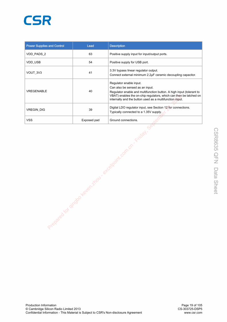
Power Supplies and Control Lead Description
CHG_EXT 43External battery charger control.External battery charger transistor base control when using externalcharger boost. Otherwise leave unconnected.
LX_1V35 50 1.35V switch-mode power regulator inductor connection.
LX_1V8 47 1.8V switch-mode power regulator inductor connection.
SMPS_1V35_SENSE 52 1.35V switch-mode power regulator sense input.
SMPS_1V8_SENSE 53 1.8V switch-mode power regulator sense input.
Production Information© Cambridge Silicon Radio Limited 2013Confidential Information - This Material is Subject to CSR's Non-disclosure Agreement
Page 17 of 105CS-303725-DSP5
www.csr.com
CSR
8635 QFN D
ata Sheet
Prepa
red
for q
ingbo
keve
n.zh
ou -
exce
lpoint
.com
.cn -
Friday
, Sep
tem
ber 2
7, 2
013

Power Supplies and Control Lead Description
SMP_BYP 49Supply via bypass regulator for 1.8V and 1.35V switchmode powersupply regulator inputs. Must be connected to the same potential asVOUT_3V3.
SMP_VBAT 481.8V and 1.35V switch-mode power supply regulator inputs.Must be at the same potential as VBAT.
VSS_SMPS_1V35 51 1.35V switch-mode regulator ground.
VSS_SMPS_1V8 46 1.8V switch-mode regulator ground.
VBAT 45 Battery positive terminal.
VBAT_SENSE 44 Battery charger sense input, connect as Section 12 shows.
VCHG 42Charger input.Typically connected to VBUS (USB supply) as Section 12 shows.
VDD_ANA 17Analogue LDO linear regulator output (1.35V).Connect to 1.35V supply, see Section 12 for connections.
VDD_AUDIO 3Positive supply for audio.Connect to 1.35V supply, see Section 12 for connections.
VDD_AUDIO_DRV 8Positive supply for audio output amplifiers.Connect to 1.8V supply, see Section 12 for connections.
VDD_AUX 14Auxiliary supply.Connect to 1.35V supply, see Section 12 for connections.
VDD_AUX_1V8 15, 16Auxiliary LDO regulator input.Connect to 1.8V supply, see Section 12 for connections.
VDD_BT_LO 13Bluetooth radio local oscillator supply (1.35V).Connect to 1.35V supply, see Section 12 for connections.
VDD_BT_RADIO 11Bluetooth radio supply.Connect to 1.35V supply, see Section 12 for connections.
VDD_DIG 38 Digital LDO regulator output, see Section 12 for connections.
VDD_PADS_1 33 Positive supply input for input/output ports.
Production Information© Cambridge Silicon Radio Limited 2013Confidential Information - This Material is Subject to CSR's Non-disclosure Agreement
Page 18 of 105CS-303725-DSP5
www.csr.com
CSR
8635 QFN D
ata Sheet
Prepa
red
for q
ingbo
keve
n.zh
ou -
exce
lpoint
.com
.cn -
Friday
, Sep
tem
ber 2
7, 2
013
Power Supplies and Control Lead Description
VDD_PADS_2 63 Positive supply input for input/output ports.
VDD_USB 54 Positive supply for USB port.
VOUT_3V3 413.3V bypass linear regulator output.Connect external minimum 2.2µF ceramic decoupling capacitor.
VREGENABLE 40
Regulator enable input.Can also be sensed as an input.Regulator enable and multifunction button. A high input (tolerant toVBAT) enables the on-chip regulators, which can then be latched oninternally and the button used as a multifunction input.
VREGIN_DIG 39Digital LDO regulator input, see Section 12 for connections.Typically connected to a 1.35V supply.
VSS Exposed pad Ground connections.
Production Information© Cambridge Silicon Radio Limited 2013Confidential Information - This Material is Subject to CSR's Non-disclosure Agreement
Page 19 of 105CS-303725-DSP5
www.csr.com
CSR
8635 QFN D
ata Sheet
Prepa
red
for q
ingbo
keve
n.zh
ou -
exce
lpoint
.com
.cn -
Friday
, Sep
tem
ber 2
7, 2
013
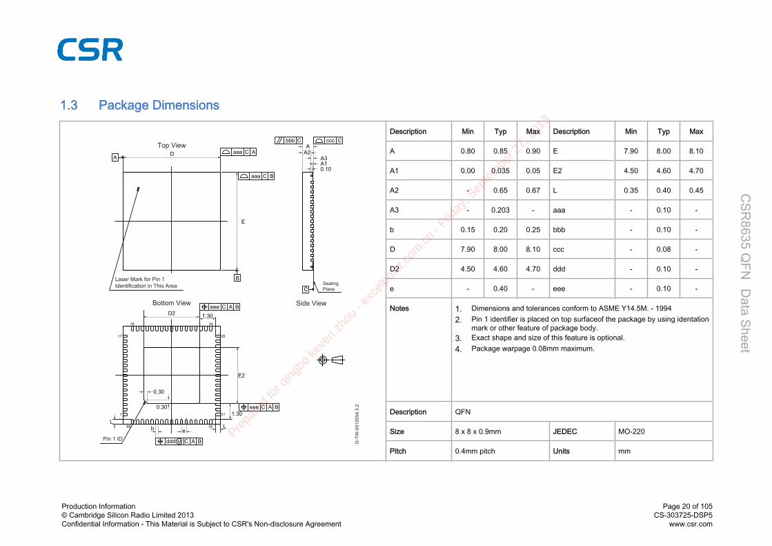
1.3 Package Dimensions
G-T
W-0
0120
54.3
.2
Seating Plane
Pin 1 ID
Laser Mark for Pin 1 Identification in This Area
A1
A
A3
0.10
A2
ccc Cbbb C
aaa C A
eee C A
A D
E
aaa C B
B
B
eee C
L
A B
ddd C
eb
1
68 52
51
35
3418
17
M A B
D2
E2
1.30
1.300.30
0.30
Top View
Bottom View Side View
L
Description Min Typ Max Description Min Typ Max
A 0.80 0.85 0.90 E 7.90 8.00 8.10
A1 0.00 0.035 0.05 E2 4.50 4.60 4.70
A2 - 0.65 0.67 L 0.35 0.40 0.45
A3 - 0.203 - aaa - 0.10 -
b 0.15 0.20 0.25 bbb - 0.10 -
D 7.90 8.00 8.10 ccc - 0.08 -
D2 4.50 4.60 4.70 ddd - 0.10 -
e - 0.40 - eee - 0.10 -
Notes 1. Dimensions and tolerances conform to ASME Y14.5M. - 19942. Pin 1 identifier is placed on top surfaceof the package by using identation
mark or other feature of package body.3. Exact shape and size of this feature is optional.4. Package warpage 0.08mm maximum.
Description QFN
Size 8 x 8 x 0.9mm JEDEC MO-220
Pitch 0.4mm pitch Units mm
Production Information© Cambridge Silicon Radio Limited 2013Confidential Information - This Material is Subject to CSR's Non-disclosure Agreement
Page 20 of 105CS-303725-DSP5
www.csr.com
CSR
8635 QFN D
ata Sheet
Prepa
red
for q
ingbo
keve
n.zh
ou -
exce
lpoint
.com
.cn -
Friday
, Sep
tem
ber 2
7, 2
013

1.4 PCB Design and Assembly ConsiderationsThis section lists recommendations to achieve maximum board-level reliability of the 8 x 8 x 0.9mm QFN 68-leadpackage:
NSMD lands (lands smaller than the solder mask aperture) are preferred, because of the greater accuracy ofthe metal definition process compared to the solder mask process. With solder mask defined pads, the overlapof the solder mask on the land creates a step in the solder at the land interface, which can cause stressconcentration and act as a point for crack initiation.
CSR recommends that the PCB land pattern is in accordance with IPC standard IPC-7351. Solder paste must be used during the assembly process.
1.5 Typical Solder Reflow ProfileFor information, see Typical Solder Reflow Profile for Lead-free Devices Information Note.
Production Information© Cambridge Silicon Radio Limited 2013Confidential Information - This Material is Subject to CSR's Non-disclosure Agreement
Page 21 of 105CS-303725-DSP5
www.csr.com
CSR
8635 QFN D
ata Sheet
Prepa
red
for q
ingbo
keve
n.zh
ou -
exce
lpoint
.com
.cn -
Friday
, Sep
tem
ber 2
7, 2
013

2 Bluetooth Modem2.1 RF Ports2.1.1 BT_RFCSR8635 QFN contains an on-chip balun which combines the balanced outputs of the PA on transmit and producesthe balanced input signals for the LNA required on receive. No matching components are needed as the receive modeimpedance is 50Ω and the transmitter has been optimised to deliver power into a 50Ω load.
G-T
W-0
0055
23.2
.2
+
_PA
+
_LNA
BT_RFOn-chip Balun
VDD
VSS_BT_RF
Figure 2.1: Simplified Circuit BT_RF
2.2 RF ReceiverThe receiver features a near-zero IF architecture that enables the channel filters to be integrated onto the die. Sufficientout-of-band blocking specification at the LNA input enables the receiver to operate in close proximity to GSM andW‑CDMA cellular phone transmitters without being desensitised. A digital FSK discriminator means that nodiscriminator tank is needed and its excellent performance in the presence of noise enables CSR8635 QFN to exceedthe Bluetooth requirements for co‑channel and adjacent channel rejection.
For EDR, the demodulator contains an ADC which digitises the IF received signal. This information is then passed tothe EDR modem.
2.2.1 Low Noise AmplifierThe LNA operates in differential mode and takes its input from the balanced port of the on-chip balun.
2.2.2 RSSI Analogue to Digital ConverterThe ADC implements fast AGC. The ADC samples the RSSI voltage on a slot-by-slot basis. The front-end LNA gainis changed according to the measured RSSI value, keeping the first mixer input signal within a limited range. Thisimproves the dynamic range of the receiver, improving performance in interference-limited environments.
2.3 RF Transmitter2.3.1 IQ ModulatorThe transmitter features a direct IQ modulator to minimise frequency drift during a transmit timeslot, which results in acontrolled modulation index. Digital baseband transmit circuitry provides the required spectral shaping.
Production Information© Cambridge Silicon Radio Limited 2013Confidential Information - This Material is Subject to CSR's Non-disclosure Agreement
Page 22 of 105CS-303725-DSP5
www.csr.com
CSR
8635 QFN D
ata Sheet
Prepa
red
for q
ingbo
keve
n.zh
ou -
exce
lpoint
.com
.cn -
Friday
, Sep
tem
ber 2
7, 2
013

2.3.2 Power AmplifierThe internal PA output power is software controlled and configured through a PS Key. The internal PA on the CSR8635QFN has a maximum output power that enables it to operate as a Class 1, Class 2 and Class 3 Bluetooth radio withoutrequiring an external RF PA.
2.4 Bluetooth Radio SynthesiserThe Bluetooth radio synthesiser is fully integrated onto the die with no requirement for an external VCO screening can,varactor tuning diodes, LC resonators or loop filter. The synthesiser is guaranteed to lock in sufficient time across theguaranteed temperature range to meet the Bluetooth v4.0 specification.
2.5 Baseband2.5.1 Burst Mode ControllerDuring transmission the BMC constructs a packet from header information previously loaded into memory-mappedregisters by the software and payload data/voice taken from the appropriate ring buffer in the RAM. During reception,the BMC stores the packet header in memory-mapped registers and the payload data in the appropriate ring buffer inRAM. This architecture minimises the intervention required by the processor during transmission and reception.
2.5.2 Physical Layer Hardware EngineDedicated logic performs:
Forward error correction Header error control Cyclic redundancy check Encryption Data whitening Access code correlation Audio transcoding
Firmware performs the following voice data translations and operations: A-law/µ-law/linear voice data (from host) A-law/µ-law/CVSD (over the air) Voice interpolation for lost packets Rate mismatch correction
The hardware supports all optional and mandatory features of the Bluetooth v4.0 specification including AFH andeSCO.
Production Information© Cambridge Silicon Radio Limited 2013Confidential Information - This Material is Subject to CSR's Non-disclosure Agreement
Page 23 of 105CS-303725-DSP5
www.csr.com
CSR
8635 QFN D
ata Sheet
Prepa
red
for q
ingbo
keve
n.zh
ou -
exce
lpoint
.com
.cn -
Friday
, Sep
tem
ber 2
7, 2
013

3 Clock GenerationCSR8635 QFN accepts a reference clock input from either a crystal or an external clock source, e.g. a TCXO.
The external reference clock is required in active and deep sleep modes and must be present when CSR8635 QFN isenabled.
3.1 CrystalCSR8635 QFN contains a crystal driver circuit that acts as a transconductance amplifier that drives an external crystalconnected between XTAL_IN and XTAL_OUT. The crystal driver circuit forms a Pierce oscillator with the externalcrystal. External capacitors are not required for standard crystals that require a load capacitance of around 9pF.CSR recommends this option.
G-T
W-0
0114
78.2
.2
External Crystal
gm
Amplifier gmControl LVL[3:0]
On-chip Capacitance Control
XTAL_IN XTAL_OUT
Figure 3.1: Crystal Oscillator Overview
The on-chip capacitance is adjusted using PSKEY_XTAL_OSC_CONFIG, see Table 3.1. The default values suit atypical crystal requiring a 9pF load capacitance. In deep sleep mode, the crystal oscillation is maintained, but at a lowerdrive strength to reduce power consumption. The drive strength and load capacitance are configured with a PS Key.
Normal ModePSKEY_XTAL_OSC_CONFIG [3:2]
Low Power ModePSKEY_XTAL_OSC_CONFIG [1:0]
Value 00 01 10 11 00 01 10 11
XTAL_IN(Typical)
15.6 pF 10.8 pF 6.0 pF 1.1 pF 15.6 pF 10.8 pF 6.0 pF 1.1 pF
XTAL_OUT(Typical)
20.8 pF 16.0 pF 11.2 pF 6.4 pF 16.0 pF 11.2 pF 6.4 pF 1.5 pF
Table 3.1: Typical On-chip Capacitance Values
The drive strength is configured with PSKEY_XTAL_LVL. The default level for this PS Key is sufficient for typicalcrystals. The level control is set in the range 0 to 15, where 15 is the maximum drive level.
Increasing the crystal amplifier drive level increases the transconductance of the crystal amplifier, which creates anincrease in the oscillator margin (ratio of oscillator amplifiers is equivalent to the negative resistance of the crystalESR).
Production Information© Cambridge Silicon Radio Limited 2013Confidential Information - This Material is Subject to CSR's Non-disclosure Agreement
Page 24 of 105CS-303725-DSP5
www.csr.com
CSR
8635 QFN D
ata Sheet
Prepa
red
for q
ingbo
keve
n.zh
ou -
exce
lpoint
.com
.cn -
Friday
, Sep
tem
ber 2
7, 2
013

Note:
Excessive amplifier transconductance can lead to an increase in the oscillator phase noise if the oscillator amplifieris excessively overdriven. Set the transconductance to the minimum level to give the desired oscillation ratio. Highervalues can increase power consumption. Also, insufficient drive strength can prevent the the crystal from startingto oscillate.
3.1.1 Negative Resistance ModelThe crystal and its load capacitor can be modelled as a frequency dependant resistive element. Consider the driveramplifier as a circuit that provides negative resistance. For oscillation, the value of the negative resistance should begreater than that of the crystal circuit equivalence resistance. Equation 3.1 shows how to calculate the equivalentnegative resistance.
Rneg=−gmCinCout
2πf2(CoutCin+(C0+Cint)(Cout+Cin))2
Equation 3.1: Negative Resistance
Where: gm = Transconductance of the crystal oscillator amplifier Co = Static capacitance of the crystal, which is sometimes referred to as the shunt or case capacitance Cint = On-chip parasitic capacitance between input and output of XTAL amplifier. Cin = Internal capacitance on XTAL_IN, see Table 3.1 Cout = Internal capacitance on XTAL_OUT, see Table 3.1
Parameter Min Typ Max Unit
Transconductance 2 - - mS
Cint - 1.5 - pF
Table 3.2: Transconductance and On-chip Parasitic Capacitance
3.1.2 Crystal SpecificationTable 3.3 shows the specification for an external crystal.
Parameter Min Typ Max Unit
Frequency 16 26 32 MHz
Initial Frequency error from nominal frequencywhich can be compensated for - - ±285 ppm
Frequency Stability - - ±20 ppm
Crystal ESR - - 60 Ω
Table 3.3: Crystal Specification
3.1.3 Crystal CalibrationThe actual crystal frequency depends on the capacitance of XTAL_IN and XTAL_OUT on the PCB and the CSR8635QFN, as well as the capacitance of the crystal.
The Bluetooth specification requires ±20ppm clock accuracy. The actual frequency at which a crystal oscillates containstwo error terms, which are typically mentioned in the crystal device datasheets:
Production Information© Cambridge Silicon Radio Limited 2013Confidential Information - This Material is Subject to CSR's Non-disclosure Agreement
Page 25 of 105CS-303725-DSP5
www.csr.com
CSR
8635 QFN D
ata Sheet
Prepa
red
for q
ingbo
keve
n.zh
ou -
exce
lpoint
.com
.cn -
Friday
, Sep
tem
ber 2
7, 2
013

Initial Frequency Error: The difference between the desired frequency and the actual oscillating frequencycaused by the crystal itself and its PCB connections. It is also called as Calibration Tolerance or FrequencyTolerance.
Frequency Stability: The total of how far the crystal can move off frequency with temperature, aging or othereffects. It is also called as Temperature Stability, Frequency Stability or Aging.
CSR8635 QFN has the capability to compensate for Initial Frequency errors by a simple per-device basis on theproduction line, with the trim value stored in the non-volatile memory (PS Key). However, it is not possible to compensatefor frequency stability, therefore a crystal must be chosen with a Frequency Stability that is better than ±20 ppm clockaccuracy.
Some crystal datasheets combine both these terms into one tolerance value. This causes a problem because only theinitial frequency error can be compensated for and CSR8635 QFN cannot compensate for the temperature or agingperformance. If frequency stability is not explicity stated, CSR cannot guarantee remaining within the Bluetooth's±20ppm frequency accuracy specification.
Crystal calibration uses a single measurement of RF output frequency and can be performed quickly as part of theproduct final test. Typically, a TXSTART radio command is sent and then a measurement of the output RF frequencyis read . From this, the calibration factor to correct actual offset from the desired frequency can be calculated. Thisoffset value is stored in PSKEY_ANA_FTRIM_OFFSET. CSR8635 QFN then compensates for the initial frequencyoffset of the crystal.
The value in PSKEY_ANA_FTRIM_OFFSET is a 16-bit 2's complement signed integer which specifies the fractionalpart of the ratio between the true crystal frequency, factual, and the value set in PSKEY_ANA_FREQ, fnominal. Equation3.2 shows the value of PSKEY_ANA_FTRIM_OFFSET in parts per 220 rounded to the nearest integer.
For more information on TXSTART radio test see BlueTest User Guide.
PSKEY_ANA_FTRIM_OFFSET = (factual
fnominal− 1) × 220
Equation 3.2: Crystal Calibration Using PSKEY_ANA_FTRIM_OFFSET
3.2 Non-crystal OscillatorApply the external reference clock to the CSR8635 QFN XTAL_IN input. Connect XTAL_OUT to ground.
The external clock is either a low-level sinusoid, or a digital-level square wave. The clock must meet the specificationin Table 3.4. The external reference clock is required in active and deep sleep modes, it must be present when CSR8635QFN is enabled.
Production Information© Cambridge Silicon Radio Limited 2013Confidential Information - This Material is Subject to CSR's Non-disclosure Agreement
Page 26 of 105CS-303725-DSP5
www.csr.com
CSR
8635 QFN D
ata Sheet
Prepa
red
for q
ingbo
keve
n.zh
ou -
exce
lpoint
.com
.cn -
Friday
, Sep
tem
ber 2
7, 2
013

Min Typ Max Unit
Frequency(a) 19.2 26 40 MHz
Duty cycle 40:60 50:50 60:40 -
Edge jitter (at zero crossing) - - 10 psrms(b)
Signal level
AC coupled sinusoidamplitude 0.2 0.4 VDD_AUX(c) V
DC coupled digitalextremes 0 - VDD_AUX(c) V
DC coupled digitaldigital amplitude 0.4 - 1.2 V pk-pk
XTAL_IN input impedance 30 - - kΩ
XTAL_IN input capacitance - - 1 pF
Table 3.4: External Clock Specifications(a) The frequency should be an integer multiple of 250kHz except for the CDMA/3G frequencies(b) 100Hz to 1MHz(c) VDD_AUX is 1.35V nominal
3.2.1 XTAL_IN Impedance in Non-crystal ModeThe impedance of XTAL_IN does not change significantly between operating modes. When transitioning from deepsleep to active states, the capacitive load can change. For this reason, CSR recommends using a buffered clock input.
Production Information© Cambridge Silicon Radio Limited 2013Confidential Information - This Material is Subject to CSR's Non-disclosure Agreement
Page 27 of 105CS-303725-DSP5
www.csr.com
CSR
8635 QFN D
ata Sheet
Prepa
red
for q
ingbo
keve
n.zh
ou -
exce
lpoint
.com
.cn -
Friday
, Sep
tem
ber 2
7, 2
013

4 Bluetooth Stack MicrocontrollerThe CSR8635 QFN uses a 16-bit RISC 80MHz MCU for low power consumption and efficient use of memory. It containsa single-cycle multiplier and a memory protection unit for the VM accelerator, see Section 4.1.
The MCU, interrupt controller and event timer run the Bluetooth software stack and control the Bluetooth radio and hostinterfaces.
4.1 VM AcceleratorCSR8635 QFN contains a VM accelerator alongside the MCU. This hardware accelerator improves the performanceof VM applications.
Production Information© Cambridge Silicon Radio Limited 2013Confidential Information - This Material is Subject to CSR's Non-disclosure Agreement
Page 28 of 105CS-303725-DSP5
www.csr.com
CSR
8635 QFN D
ata Sheet
Prepa
red
for q
ingbo
keve
n.zh
ou -
exce
lpoint
.com
.cn -
Friday
, Sep
tem
ber 2
7, 2
013

5 Kalimba DSPThe Kalimba DSP is an open platform DSP enabling signal processing functions to be performed on over‑air data orcodec data to enhance audio applications. Figure 5.1 shows the Kalimba DSP interfaces to other functional blockswithin CSR8635 QFN.
G-T
W-0
0055
22.2
.2
MemoryManagement
Unit
MCU Register Interface (including Debug)
DSP MMU Port
PIO In/Out
IRQ to Subsystem
IRQ from Subsystem
1µs Timer Clock
Programmable Clock = 80MHz
Data MemoryInteface
AddressGenerators
Instruction Decode
Program Flow
Clock Select
Internal Control Register
MMU Interface
Interrupt Controller
Timer
MCU Window
Flash Window
DEBUG
ALU
PIO
DS
P P
rogr
am C
ontro
l
Reg
iste
rs
DSP RAMs
DM2
DM1
PM
Kalimba DSP Core
DSP, MCU and Memory Window Control
DSP Data Memory 2 Interface (DM2)
DSP Data Memory 1 Interface (DM1)
DSP Program Memory Interface (PM)
Figure 5.1: Kalimba DSP Interface to Internal Functions
The key features of the DSP include: 80MIPS performance, 24‑bit fixed point DSP core Single‑cycle MAC; 24 x 24‑bit multiply and 56‑bit accumulate includes 2 rMAC registers and new instructions
for improved performance over previous architecture 32‑bit instruction word Separate program memory and dual data memory, enabling an ALU operation and up to 2 memory accesses
in a single cycle Zero overhead looping, including a very low‑power 32‑instruction cache Zero overhead circular buffer indexing Single cycle barrel shifter with up to 56‑bit input and 56‑bit output Multiple cycle divide (performed in the background) Bit reversed addressing Orthogonal instruction set Low overhead interrupt
For more information see Kalimba Architecture 3 DSP User Guide.
Production Information© Cambridge Silicon Radio Limited 2013Confidential Information - This Material is Subject to CSR's Non-disclosure Agreement
Page 29 of 105CS-303725-DSP5
www.csr.com
CSR
8635 QFN D
ata Sheet
Prepa
red
for q
ingbo
keve
n.zh
ou -
exce
lpoint
.com
.cn -
Friday
, Sep
tem
ber 2
7, 2
013
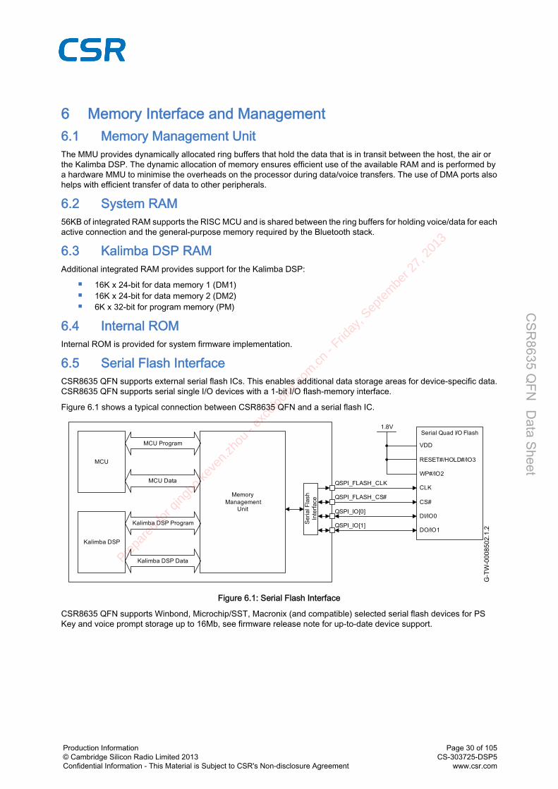
6 Memory Interface and Management6.1 Memory Management UnitThe MMU provides dynamically allocated ring buffers that hold the data that is in transit between the host, the air orthe Kalimba DSP. The dynamic allocation of memory ensures efficient use of the available RAM and is performed bya hardware MMU to minimise the overheads on the processor during data/voice transfers. The use of DMA ports alsohelps with efficient transfer of data to other peripherals.
6.2 System RAM56KB of integrated RAM supports the RISC MCU and is shared between the ring buffers for holding voice/data for eachactive connection and the general-purpose memory required by the Bluetooth stack.
6.3 Kalimba DSP RAMAdditional integrated RAM provides support for the Kalimba DSP:
16K x 24-bit for data memory 1 (DM1) 16K x 24-bit for data memory 2 (DM2) 6K x 32-bit for program memory (PM)
6.4 Internal ROMInternal ROM is provided for system firmware implementation.
6.5 Serial Flash InterfaceCSR8635 QFN supports external serial flash ICs. This enables additional data storage areas for device-specific data.CSR8635 QFN supports serial single I/O devices with a 1-bit I/O flash-memory interface.
Figure 6.1 shows a typical connection between CSR8635 QFN and a serial flash IC.
G-T
W-0
0085
02.1
.2Memory
ManagementUnit
Serial Quad I/O Flash
MCU Program
MCU Data
Kalimba DSP Data
Kalimba DSP Program
MCU
Kalimba DSP
QSPI_FLASH_CLK
QSPI_FLASH_CS#
QSPI_IO[0]
QSPI_IO[1]Ser
ial F
lash
Inte
rface
CLK
CS#
DI/IO0
DO/IO1
WP#/IO2
RESET#/HOLD#/IO3
1.8V
VDD
Figure 6.1: Serial Flash Interface
CSR8635 QFN supports Winbond, Microchip/SST, Macronix (and compatible) selected serial flash devices for PSKey and voice prompt storage up to 16Mb, see firmware release note for up-to-date device support.
Production Information© Cambridge Silicon Radio Limited 2013Confidential Information - This Material is Subject to CSR's Non-disclosure Agreement
Page 30 of 105CS-303725-DSP5
www.csr.com
CSR
8635 QFN D
ata Sheet
Prepa
red
for q
ingbo
keve
n.zh
ou -
exce
lpoint
.com
.cn -
Friday
, Sep
tem
ber 2
7, 2
013

7 Serial Interfaces7.1 USB InterfaceCSR8635 QFN has a full-speed (12Mbps) USB interface for communicating with other compatible digital devices. TheUSB interface on CSR8635 QFN acts as a USB peripheral, responding to requests from a master host controller.
CSR8635 QFN contains internal USB termination resistors and requires no external resistor matching.
CSR8635 QFN supports the Universal Serial Bus Specification, Revision v2.0 (USB v2.0 Specification), supportsUSB standard charger detection and fully supports the USB Battery Charging Specification, available from http://www.usb.org. For more information on how to integrate the USB interface on CSR8635 QFN see the Bluetooth andUSB Design Considerations Application Note.
As well as describing USB basics and architecture, the application note describes: Power distribution for high and low bus-powered configurations Power distribution for self-powered configuration, which includes USB VBUS monitoring USB enumeration Electrical design guidelines for the power supply and data lines, as well as PCB tracks and the effects of ferrite
beads USB suspend modes and Bluetooth low-power modes:
Global suspend Selective suspend, includes remote wake Wake on Bluetooth, includes permitted devices and set-up prior to selective suspend Suspend mode current draw PIO status in suspend mode Resume, detach and wake PIOs
Battery charging from USB, which describes dead battery provision, charge currents, charging in suspendmodes and USB VBUS voltage consideration
USB termination when interface is not in use Internal modules, certification and non-specification compliant operation
7.2 UART InterfaceCSR8635 QFN has one optional standard UART serial interface that provides a simple mechanism for communicatingwith other serial devices using the RS232 protocol, including for test and debug. The UART interface is multiplexedwith PIOs and other functions, and hardware flow control is optional. PS Keys configure this multiplexing, see Table7.1.
PS Key PIO Location Option
PSKEY_UART_RX_PIO PIO[0] (default) or PIO[14]
PSKEY_UART_TX_PIO PIO[1] (default) or PIO[15]
PSKEY_UART_RTS_PIO PIO[8] (default) or PIO[16]
PSKEY_UART_CTS_PIO PIO[9] (default) or PIO[17]
Table 7.1: PS Keys for UART/PIO Multiplexing
Production Information© Cambridge Silicon Radio Limited 2013Confidential Information - This Material is Subject to CSR's Non-disclosure Agreement
Page 31 of 105CS-303725-DSP5
www.csr.com
CSR
8635 QFN D
ata Sheet
Prepa
red
for q
ingbo
keve
n.zh
ou -
exce
lpoint
.com
.cn -
Friday
, Sep
tem
ber 2
7, 2
013

Figure 7.1 shows the 4 signals that implement the UART function.
G-T
W-0
0085
55.2
.2
PIO[1] or PIO[15]
PIO[0] or PIO[14]
PIO[8] or PIO[16]
PIO[9] or PIO[17]
UART_TX
UART_RX
UART_RTS
UART_CTS
Figure 7.1: Universal Asynchronous Receiver
When CSR8635 QFN is connected to another digital device, UART_RX and UART_TX transfer data between the 2devices. The remaining 2 signals, UART_CTS and UART_RTS, implement optional RS232 hardware flow control whereboth are active low indicators.
UART configuration parameters, such as baud rate and packet format, are set using CSR8635 QFN firmware.
Note:
To communicate with the UART at its maximum data rate using a standard PC, the PC requires an acceleratedserial port adapter card.
Table 7.2 shows the possible UART settings.
Parameter Possible Values
Baud rateMinimum
1200 baud (≤2%Error)
9600 baud (≤1%Error)
Maximum 4Mbaud (≤1%Error)
Flow control RTS/CTS or None
Parity None, Odd or Even
Number of stop bits 1 or 2
Bits per byte 8
Table 7.2: Possible UART Settings
Table 7.3 lists common baud rates and their associated values for the PSKEY_UART_BAUDRATE. There is norequirement to use these standard values. Any baud rate within the supported range is set in the PS Key according tothe formula in Equation 7.1.
Baud Rate = PSKEY_UART_BAUDRATE0.004096
Equation 7.1: Baud Rate
Production Information© Cambridge Silicon Radio Limited 2013Confidential Information - This Material is Subject to CSR's Non-disclosure Agreement
Page 32 of 105CS-303725-DSP5
www.csr.com
CSR
8635 QFN D
ata Sheet
Prepa
red
for q
ingbo
keve
n.zh
ou -
exce
lpoint
.com
.cn -
Friday
, Sep
tem
ber 2
7, 2
013

Baud RatePersistent Store Value
ErrorHex Dec
1200 0x0005 5 1.73%
2400 0x000a 10 1.73%
4800 0x0014 20 1.73%
9600 0x0027 39 -0.82%
19200 0x004f 79 0.45%
38400 0x009d 157 -0.18%
57600 0x00ec 236 0.03%
76800 0x013b 315 0.14%
115200 0x01d8 472 0.03%
230400 0x03b0 944 0.03%
460800 0x075f 1887 -0.02%
921600 0x0ebf 3775 0.00%
1382400 0x161e 5662 -0.01%
1843200 0x1d7e 7550 0.00%
2764800 0x2c3d 11325 0.00%
3686400 0x3afb 15099 0.00%
Table 7.3: Standard Baud Rates
7.3 Programming and Debug InterfaceCSR8635 QFN provides a debug SPI interface for programming, configuring (PS Keys) and debugging the CSR8635QFN. Access to this interface is required in production. Ensure the 4 SPI signals and the SPI_PCM# line are broughtout to either test points or a header. To use the SPI interface, the SPI_PCM# line requires the option of being pulledhigh externally.
CSR provides development and production tools to communicate over the SPI from a PC, although a level translatorcircuit is often required. All are available from CSR.
7.3.1 Multi-slave OperationAvoid connecting CSR8635 QFN in a multi-slave arrangement by simple parallel connection of slave MISO lines. WhenCSR8635 QFN is deselected (SPI_CS# = 1), the SPI_MISO line does not float. Instead, CSR8635 QFN outputs 0 ifthe processor is running or 1 if it is stopped.
Production Information© Cambridge Silicon Radio Limited 2013Confidential Information - This Material is Subject to CSR's Non-disclosure Agreement
Page 33 of 105CS-303725-DSP5
www.csr.com
CSR
8635 QFN D
ata Sheet
Prepa
red
for q
ingbo
keve
n.zh
ou -
exce
lpoint
.com
.cn -
Friday
, Sep
tem
ber 2
7, 2
013

7.4 I²C EEPROM InterfaceCSR8635 QFN supports optional I²C EEPROM for storage of PS Keys and voice prompt data if SPI flash is not used.Figure 7.2 shows an example I²C EEPROM connection where:
PIO[10] is the I²C EEPROM SCL line PIO[11] is the I²C EEPROM SDA line PIO[12] is the I²C EEPROM WP line
G-T
W-0
0085
57.1
.1
1.8V
10nF
C1
PIO[11]/QSPI_IO[0]/I2C_SDAPIO[10]/QSPI_FLASH_CLK/I2C_SCL
24AAxxx
VCC8
VSS 4A2 3SCL6 A1 2A0 1
WP7
SDA5
U1
PIO[12]/QSPI_FLASH_CS#/I2C_WP
2.2kΩR3
2.2kΩR2
2.2kΩR1
Figure 7.2: Example I²C EEPROM Connection
Note:
The I²C EEPROM requires external pull-up resistors, see Figure 7.2. Ensure that external pull-up resistors aresuitably sized for the I²C interface speed and PCB track capacitance.
To minimise boot time, CSR recommends using 400kHz capable I²C EEPROMs and I2C_CONFIG andANA_FREQ should be the first 2 keys in the EEPROM PS-store image.
EEPROMs must be suitable for operation at 1.8V.
Production Information© Cambridge Silicon Radio Limited 2013Confidential Information - This Material is Subject to CSR's Non-disclosure Agreement
Page 34 of 105CS-303725-DSP5
www.csr.com
CSR
8635 QFN D
ata Sheet
Prepa
red
for q
ingbo
keve
n.zh
ou -
exce
lpoint
.com
.cn -
Friday
, Sep
tem
ber 2
7, 2
013

8 Interfaces8.1 Programmable I/O Ports, PIOCSR8635 QFN provides 22 lines of programmable bidirectional I/O, PIO[21:0]. Some of the PIOs on the CSR8635QFN have alternative functions, see Table 8.1.
PIO
Function
Debug SPI(See Section 7.3)
SPI Flash(See Section 6.5)
UART(See Section 7.2)
PCM(See Section 9.3)
EEPROM(See Section 7.4)
PIO[0] - - UART_RX (default) - -
PIO[1] - - UART_TX (default) - -
PIO[2] SPI_MOSI - - PCM1_IN -
PIO[3] SPI_MISO - - PCM1_OUT -
PIO[4] SPI_CS# - - PCM1_SYNC -
PIO[5] SPI_CLK - - PCM1_CLK -
PIO[8] - - UART_RTS (default) - -
PIO[9] - - UART_CTS (default) - -
PIO[10] - QSPI_FLASH_CLK - - I2C_SCL
PIO[11] - QSPI_IO[0] - - I2C_SDA
PIO[12] - QSPI_FLASH_CS# - - I2C_WP
PIO[13] - QSPI_IO[1] - - -
PIO[14] - - UART_RX - -
PIO[15] - - UART_TX - -
PIO[16] - - UART_RTS - -
PIO[17] - - UART_CTS - -
Table 8.1: Alternative PIO Functions
Note:
See the relevant software release note for the implementation of these PIO lines, as they are firmware build-specific.
8.2 Analogue I/O Ports, AIOCSR8635 QFN has 1 general-purpose analogue interface pin, AIO[0]. Typically, this connects to a thermistor for batterypack temperature measurements during charge control. See Section 12 for typical connections.
8.3 LED DriversCSR8635 QFN includes a 3-pad synchronised PWM LED driver for driving RGB LEDs for producing a wide range ofcolours. All LEDs are controlled by firmware.
Production Information© Cambridge Silicon Radio Limited 2013Confidential Information - This Material is Subject to CSR's Non-disclosure Agreement
Page 35 of 105CS-303725-DSP5
www.csr.com
CSR
8635 QFN D
ata Sheet
Prepa
red
for q
ingbo
keve
n.zh
ou -
exce
lpoint
.com
.cn -
Friday
, Sep
tem
ber 2
7, 2
013

The terminals are open-drain outputs, so the LED must be connected from a positive supply rail to the pad in serieswith a current-limiting resistor.
G-T
W-0
0055
34.2
.2
LED Forward Voltage, VF
Pad Voltage, VPAD; RON = 20Ω
RLED
LED[2, 1 or 0]Resistor Voltage Drop, VR
LED Supply
I LED
Figure 8.1: LED Equivalent Circuit
From Figure 8.1 it is possible to derive Equation 8.1 to calculate ILED. If a known value of current is required throughthe LED to give a specific luminous intensity, then the value of RLED is calculated.
ILED =VDD − VF
RLED + RON
Equation 8.1: LED Current
For the LED pads to act as resistance, the external series resistor, RLED, needs to be such that the voltage drop acrossit, VR, keeps VPAD below 0.5V. Equation 8.2 also applies.
VDD = VF + VR + VPAD
Equation 8.2: LED PAD Voltage
Note:
The supply domain in Section 1.2 for LED[2:0] must remain powered for LED functions to operate.
The LED current adds to the overall current. Conservative LED selection extends battery life.
Production Information© Cambridge Silicon Radio Limited 2013Confidential Information - This Material is Subject to CSR's Non-disclosure Agreement
Page 36 of 105CS-303725-DSP5
www.csr.com
CSR
8635 QFN D
ata Sheet
Prepa
red
for q
ingbo
keve
n.zh
ou -
exce
lpoint
.com
.cn -
Friday
, Sep
tem
ber 2
7, 2
013

9 Audio InterfaceThe audio interface circuit consists of:
Stereo/dual-mono audio codec Dual analogue audio inputs Dual analogue audio outputs Configurable PCM (PCM1) and I²S interfaces, for configuration information contact CSR
Figure 9.1 shows the functional blocks of the interface. The codec supports stereo/dual-mono playback and recordingof audio signals at multiple sample rates with a 16-bit resolution. The ADC and the DAC of the codec each contain 2independent high-quality channels. Any ADC or DAC channel runs at its own independent sample rate.
G-T
W-0
0129
78.1
.1
Stereo / Dual-mono Codec
Memory Management
Unit
MMU Voice Port
Register Interface
Voice Port
Registers
PCM1
Digital Audio
StereoAudioCodecDriver
PCM1 Interface
2 x DifferentialDAC Outputs
2 x DifferentialADC Inputs
Figure 9.1: Audio Interface
The interface for the digital audio bus shares the same pins as the PCM1 codec interface described in Section 9.3.Table 9.1 lists the alternative functions.
Important Note:
The term PCM in Section 9.3 and its subsections refers to the PCM1 interface.
PCM Interface I²S Interface
PCM_OUT SD_OUT
PCM_IN SD_IN
PCM_SYNC WS
PCM_CLK SCK
Table 9.1: Alternative Functions of the Digital Audio Bus Interface on the PCM1 Interface
9.1 Audio Input and OutputThe audio input circuitry consists of 2 independent 16-bit high-quality ADC channels:
Programmable as either stereo or dual-mono inputs 1 input programmable as either microphone or line input, the other as line input only Each channel is independently configurable to be either single-ended or fully differential Each channel has an analogue and digital programmable gain stage, this also aids optimisation of different
microphones
The audio output circuitry consists of a dual differential class A-B output stage.
Production Information© Cambridge Silicon Radio Limited 2013Confidential Information - This Material is Subject to CSR's Non-disclosure Agreement
Page 37 of 105CS-303725-DSP5
www.csr.com
CSR
8635 QFN D
ata Sheet
Prepa
red
for q
ingbo
keve
n.zh
ou -
exce
lpoint
.com
.cn -
Friday
, Sep
tem
ber 2
7, 2
013

Note:
CSR8635 QFN is designed for a differential audio output. If a single-ended audio output is required, use an externaldifferential to single-ended converter.
9.2 Audio Codec InterfaceThe main features of the interface are:
Stereo and mono analogue input for voice band and audio band Stereo and mono analogue output for voice band and audio band Support for I²S stereo digital audio bus standard Support for PCM interface including PCM master codecs that require an external system clock
Important Note:
To avoid any confusion regarding stereo operation this data sheet explicitly states which is the left and right channelfor audio output. With respect to audio input, software and any registers, channel 0 or channel A represents theleft channel and channel 1 or channel B represents the right channel.
9.2.1 Audio Codec Block Diagram
G-T
W-0
0129
79.2
.2
Input B
Input A
High-quality ADC
High-quality ADC
16
16
LINE_BPLINE_BN
LINE/MIC_APLINE/MIC_AN
Digital Codec
Digital Codec
Stereo Audio and Voice Band Output
High-quality DAC
Low-pass Filter
SPKR_LNSPKR_LP
16
High-quality DACSPKR_RNSPKR_RP
16
Digital CircuitryStereo Audio and Voice Band Input
Low-pass Filter
Figure 9.2: Audio Codec Input and Output Stages
The CSR8635 QFN audio codec uses a fully differential architecture in the analogue signal path, which results in lownoise sensitivity and good power supply rejection while effectively doubling the signal amplitude. It operates from adual power supply, VDD_AUDIO for the audio circuits and VDD_AUDIO_DRV for the audio driver circuits.
9.2.2 ADCFigure 9.2 shows the CSR8635 QFN consists of 2 high-quality ADCs:
Each ADC has a second-order Sigma-Delta converter. Each ADC is a separate channel with identical functionality. There are 2 gain stages for each channel, 1 of which is an analogue gain stage and the other is a digital gain
stage, see Section 9.2.4.
9.2.3 ADC Sample Rate SelectionEach ADC supports the following pre-defined sample rates, although other rates are programmable, e.g. 40kHz:
8kHz 11.025kHz 16kHz 22.050kHz 24kHz 32kHz 44.1kHz 48kHz
Production Information© Cambridge Silicon Radio Limited 2013Confidential Information - This Material is Subject to CSR's Non-disclosure Agreement
Page 38 of 105CS-303725-DSP5
www.csr.com
CSR
8635 QFN D
ata Sheet
Prepa
red
for q
ingbo
keve
n.zh
ou -
exce
lpoint
.com
.cn -
Friday
, Sep
tem
ber 2
7, 2
013

9.2.4 ADC Audio Input Gain
G-T
W-0
0055
35.4
.3
ADC Pre-amplifierand ADC Analogue Gain:-3dB to 42dB in 3dB steps
ADC Pre-amplifier:0dB, 9dB, 21dB and 30dB
ADC Analogue Gain:-3dB to 12dB in 3dB steps
ADC Digital Gain:-24dB to 21.5dB in alternating2.5dB and 3dB steps
Audio Input To Digital Codec
System Gain = ADC Pre-amplifier + ADC Analogue Gain + ADC Digital Gain
Figure 9.3: Audio Input Gain
9.2.5 ADC Pre-amplifier and ADC Analogue Gain
CSR8635 QFN has an analogue gain stage based on an ADC pre-amplifier and ADC analogue amplifier: The ADC pre-amplifier has 4 gain settings: 0dB, 9dB, 21dB and 30dB The ADC analogue amplifier gain is -3dB to 12dB in 3dB steps The overall analogue gain for the pre-amplifier and analogue amplifier is -3dB to 42dB in 3dB steps, see Figure
9.3 At mid to high gain levels it acts as a microphone pre-amplifier, see Section 9.2.13 At low gain levels it acts as an audio line level amplifier
9.2.6 ADC Digital GainA digital gain stage inside the ADC varies from -24dB to 21.5dB, see Table 9.2. There is also a fine gain interface witha 9-bit gain setting allowing gain changes in 1/32 steps, for more information contact CSR.
The firmware controls the audio input gain.
Digital Gain SelectionValue
ADC Digital Gain Setting(dB)
Digital Gain SelectionValue
ADC Digital Gain Setting(dB)
0 0 8 -24
1 3.5 9 -20.5
2 6 10 -18
3 9.5 11 -14.5
4 12 12 -12
5 15.5 13 -8.5
6 18 14 -6
7 21.5 15 -2.5
Table 9.2: ADC Audio Input Gain Rate
Production Information© Cambridge Silicon Radio Limited 2013Confidential Information - This Material is Subject to CSR's Non-disclosure Agreement
Page 39 of 105CS-303725-DSP5
www.csr.com
CSR
8635 QFN D
ata Sheet
Prepa
red
for q
ingbo
keve
n.zh
ou -
exce
lpoint
.com
.cn -
Friday
, Sep
tem
ber 2
7, 2
013
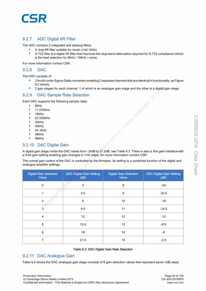
9.2.7 ADC Digital IIR FilterThe ADC contains 2 integrated anti-aliasing filters:
A long IIR filter suitable for music (>44.1kHz) G.722 filter is a digital IIR filter that improves the stop-band attenuation required for G.722 compliance (which
is the best selection for 8kHz / 16kHz / voice)
For more information contact CSR.
9.2.8 DACThe DAC consists of:
2 fourth-order Sigma-Delta converters enabling 2 separate channels that are identical in functionality, as Figure9.2 shows.
2 gain stages for each channel, 1 of which is an analogue gain stage and the other is a digital gain stage.
9.2.9 DAC Sample Rate SelectionEach DAC supports the following sample rates:
8kHz 11.025kHz 16kHz 22.050kHz 32kHz 40kHz 44.1kHz 48kHz 96kHz
9.2.10 DAC Digital GainA digital gain stage inside the DAC varies from -24dB to 21.5dB, see Table 9.3. There is also a fine gain interface witha 9-bit gain setting enabling gain changes in 1/32 steps, for more information contact CSR.
The overall gain control of the DAC is controlled by the firmware. Its setting is a combined function of the digital andanalogue amplifier settings.
Digital Gain SelectionValue
DAC Digital Gain Setting(dB)
Digital Gain SelectionValue
DAC Digital Gain Setting(dB)
0 0 8 -24
1 3.5 9 -20.5
2 6 10 -18
3 9.5 11 -14.5
4 12 12 -12
5 15.5 13 -8.5
6 18 14 -6
7 21.5 15 -2.5
Table 9.3: DAC Digital Gain Rate Selection
9.2.11 DAC Analogue GainTable 9.4 shows the DAC analogue gain stage consists of 8 gain selection values that represent seven 3dB steps.
Production Information© Cambridge Silicon Radio Limited 2013Confidential Information - This Material is Subject to CSR's Non-disclosure Agreement
Page 40 of 105CS-303725-DSP5
www.csr.com
CSR
8635 QFN D
ata Sheet
Prepa
red
for q
ingbo
keve
n.zh
ou -
exce
lpoint
.com
.cn -
Friday
, Sep
tem
ber 2
7, 2
013
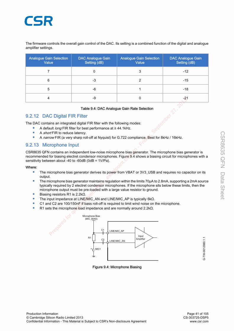
The firmware controls the overall gain control of the DAC. Its setting is a combined function of the digital and analogueamplifier settings.
Analogue Gain SelectionValue
DAC Analogue GainSetting (dB)
Analogue Gain SelectionValue
DAC Analogue GainSetting (dB)
7 0 3 -12
6 -3 2 -15
5 -6 1 -18
4 -9 0 -21
Table 9.4: DAC Analogue Gain Rate Selection
9.2.12 DAC Digital FIR FilterThe DAC contains an integrated digital FIR filter with the following modes:
A default long FIR filter for best performance at ≥ 44.1kHz. A short FIR to reduce latency. A narrow FIR (a very sharp roll-off at Nyquist) for G.722 compliance. Best for 8kHz / 16kHz.
9.2.13 Microphone InputCSR8635 QFN contains an independent low-noise microphone bias generator. The microphone bias generator isrecommended for biasing electret condensor microphones. Figure 9.4 shows a biasing circuit for microphones with asensitivity between about ‑40 to ‑60dB (0dB = 1V/Pa).
Where: The microphone bias generator derives its power from VBAT or 3V3_USB and requires no capacitor on its
output. The microphone bias generator maintains regulation within the limits 70μA to 2.8mA, supporting a 2mA source
typically required by 2 electret condensor microphones. If the microphone sits below these limits, then themicrophone output must be pre-loaded with a large value resistor to ground.
Biasing resistors R1 is 2.2kΩ. The input impedance at LINE/MIC_AN and LINE/MIC_AP is typically 6kΩ. C1 and C2 are 100/150nF if bass roll-off is required to limit wind noise on the microphone. R1 sets the microphone load impedance and are normally around 2.2kΩ.
G-T
W-0
0129
80.1
.1C2R1
C1
Microphone Bias(MIC_BIAS)
LINE/MIC_AP
LINE/MIC_AN
MIC1+
Input Amplifier
Figure 9.4: Microphone Biasing
Production Information© Cambridge Silicon Radio Limited 2013Confidential Information - This Material is Subject to CSR's Non-disclosure Agreement
Page 41 of 105CS-303725-DSP5
www.csr.com
CSR
8635 QFN D
ata Sheet
Prepa
red
for q
ingbo
keve
n.zh
ou -
exce
lpoint
.com
.cn -
Friday
, Sep
tem
ber 2
7, 2
013

The microphone bias characteristics include: Power supply:
CSR8635 QFN microphone supply is VBAT or 3V3_USB Minimum input voltage = Output voltage + drop-out voltage Maximum input voltage is 4.3V
Drop-out voltage: 300mV maximum
Output voltage: 1.8V or 2.6V Tolerance 90% to 110%
Output current: 70μA to 2.8mA
No load capacitor required
9.2.14 Line InputFigure 9.5 and Figure 9.6 show 2 circuits for line input operation and show connections for either differential or single-ended inputs.
In line input mode, the input impedance of the pins to ground varies from 6kΩ to 34kΩ depending on input gain setting.
G-T
W-0
0129
81.1
.1
C3
C4
LINE_BN
LINE_BP
C1
C2
LINE/MIC_AN
LINE/MIC_AP
Figure 9.5: Differential Input
G-T
W-0
0129
82.1
.1
C3
C4
LINE_AP
LINE_AN
C1
C2
LINE/MIC_AP
LINE/MIC_AN
Figure 9.6: Single-ended Input
9.2.15 Output StageThe output stage digital circuitry converts the signal from 16-bit per sample, linear PCM of variable sampling frequencyto bit stream, which is fed into the analogue output circuitry.
Production Information© Cambridge Silicon Radio Limited 2013Confidential Information - This Material is Subject to CSR's Non-disclosure Agreement
Page 42 of 105CS-303725-DSP5
www.csr.com
CSR
8635 QFN D
ata Sheet
Prepa
red
for q
ingbo
keve
n.zh
ou -
exce
lpoint
.com
.cn -
Friday
, Sep
tem
ber 2
7, 2
013

The analogue output circuit comprises a DAC, a buffer with gain-setting, a low-pass filter and a class AB output stageamplifier. Figure 9.7 shows that the output is available as a differential signal between SPKR_LN and SPKR_LP for theleft channel, and between SPKR_RN and SPKR_RP for the right channel.
G-T
W-0
0055
37.1
.1
SPKR_LP
SPKR_LN
SPKR_RP
SPKR_RN
Figure 9.7: Speaker Output
9.2.16 Mono OperationMono operation is a single-channel operation of the stereo codec. The left channel represents the single mono channelfor audio in and audio out. In mono operation, the right channel is the auxiliary mono channel for dual-mono channeloperation.
In single channel mono operation, disable the other channel to reduce power consumption.
9.2.17 Side ToneIn some applications it is necessary to implement side tone. This side tone function involves feeding a properly gainedmicrophone signal in to the DAC stream, e.g. earpiece. The side tone routing selects the version of the microphonesignal from before or after the digital gain in the ADC interface and adds it to the output signal before or after the digitalgain of the DAC interface, see Figure 9.8.
Production Information© Cambridge Silicon Radio Limited 2013Confidential Information - This Material is Subject to CSR's Non-disclosure Agreement
Page 43 of 105CS-303725-DSP5
www.csr.com
CSR
8635 QFN D
ata Sheet
Prepa
red
for q
ingbo
keve
n.zh
ou -
exce
lpoint
.com
.cn -
Friday
, Sep
tem
ber 2
7, 2
013

G-T
W-0
0053
75.1
.1
Side Tone Route
Digital Input Analogue Output
Digital Output Analogue Input
Digital Gain
Demux
Mux
DAC
DAC Interface
Side Tone
Digital Gain
ADC
ADC Interface
Side Tone Route
Side Tone Gain
Figure 9.8: Side Tone
The ADC provides simple gain to the side tone data. The gain values range from -32.6dB to 12.0dB in alternating stepsof 2.5dB and 3.5dB, see Table 9.5.
Value Side Tone Gain Value Side Tone Gain
0 -32.6dB 8 -8.5dB
1 -30.1dB 9 -6.0dB
2 -26.6dB 10 -2.5dB
3 -24.1dB 11 0dB
4 -20.6dB 12 3.5dB
5 -18.1dB 13 6.0dB
6 -14.5dB 14 9.5dB
7 -12.0dB 15 12.0dB
Table 9.5: Side Tone Gain
Note:
The values of side tone are shown for information only. During standard operation, the application software controlsthe side tone gain.
The following PS Keys configure the side tone hardware:
Production Information© Cambridge Silicon Radio Limited 2013Confidential Information - This Material is Subject to CSR's Non-disclosure Agreement
Page 44 of 105CS-303725-DSP5
www.csr.com
CSR
8635 QFN D
ata Sheet
Prepa
red
for q
ingbo
keve
n.zh
ou -
exce
lpoint
.com
.cn -
Friday
, Sep
tem
ber 2
7, 2
013

PSKEY_SIDE_TONE_ENABLE PSKEY_SIDE_TONE_GAIN PSKEY_SIDE_TONE_AFTER_ADC PSKEY_SIDE_TONE_AFTER_DAC
9.2.18 Integrated Digital IIR FilterCSR8635 QFN has a programmable digital filter integrated into the ADC channel of the codec. The filter is a 2-stage,second order IIR and is for functions such as custom wind noise reduction. The filter also has optional DC blocking.
The filter has 10 configuration words:
1 for gain value 8 for coefficient values 1 for enabling and disabling the DC blocking
The gain and coefficients are all 12-bit 2's complement signed integer with the format NN.NNNNNNNNNN.
Note:
The position of the binary point is between bit[10] and bit[9], where bit[11] is the most significant bit.
For example:
01.1111111111
01.0000000000
00.0000000000
11.0000000000
10.0000000000
=
=
=
=
=
most positive number, close to 21
0
-1
-2, most negative number
Equation 9.1 shows the equation for the IIR filter. Equation 9.2 shows the equation for when the DC blocking is enabled.
The filter is configured, enabled and disabled from the VM via the CodecSetIIRFilterA andCodecSetIIRFilterB traps. This requires firmware support. The configuration function takes 10 variables in thefollowing order:
0
1
2
3
4
5
6
7
8
9
:
:
:
:
:
:
:
:
:
:
Gainb01
b02
a01
a02
b11
b12
a11
a12
DC Block (1 = enable, 0 = disable)
Filter, H(z) = Gain ×( 1 + b01 z−1 + b02 z−2 )
( 1 + a01 z−1 + a02 z−2 )×
( 1 + b11 z−1 + b12 z−2 )
( 1 + a11 z−1 + a12 z−2 )
Equation 9.1: IIR Filter Transfer Function, H(z)
Filter with DC Blocking, HDC (z) = H(z) × ( 1 − z−1 )
Equation 9.2: IIR Filter Plus DC Blocking Transfer Function, HDC(z)
Production Information© Cambridge Silicon Radio Limited 2013Confidential Information - This Material is Subject to CSR's Non-disclosure Agreement
Page 45 of 105CS-303725-DSP5
www.csr.com
CSR
8635 QFN D
ata Sheet
Prepa
red
for q
ingbo
keve
n.zh
ou -
exce
lpoint
.com
.cn -
Friday
, Sep
tem
ber 2
7, 2
013

9.3 PCM1 InterfaceImportant Note:
The PCM1 interface is provided as a test interface and is only accessible when running the CSR8635 QFN in HCI-only mode.
Section 9 describes the various digital audio interfaces multiplexed on the the PCM1 interface. The PCM1 interfacealso shares the same physical set of pins with the SPI interface, see Section 7.3 and Section 8.1. Either interface isselected using SPI_PCM#:
SPI_PCM# = 1 selects SPI SPI_PCM# = 0 selects PCM
Important Note:
The term PCM refers to PCM1.
The audio PCM interface on the CSR8635 QFN supports: Continuous transmission and reception of PCM encoded audio data over Bluetooth. Processor overhead reduction through hardware support for continual transmission and reception of PCM
data. A bidirectional digital audio interface that routes directly into the baseband layer of the firmware. It does not
pass through the HCI protocol layer. Hardware on the CSR8635 QFN for sending data to and from a SCO connection. Up to 3 SCO connections on the PCM interface at any one time. PCM interface master, generating PCM_SYNC and PCM_CLK. PCM interface slave, accepting externally generated PCM_SYNC and PCM_CLK. Various clock formats including:
Long Frame Sync Short Frame Sync GCI timing environments
13-bit or 16-bit linear, 8-bit µ-law or A-law companded sample formats. Receives and transmits on any selection of 3 of the first 4 slots following PCM_SYNC.
The PCM configuration options are enabled by setting the PSKEY_PCM_CONFIG32.
9.3.1 PCM Interface Master/SlaveWhen configured as the master of the PCM interface, CSR8635 QFN generates PCM_CLK and PCM_SYNC.
G-T
W-0
0002
17.3
.4128/256/512/1536/2400kHz
8/48kHz
PCM_OUT
PCM_IN
PCM_CLK
PCM_SYNC
Figure 9.9: PCM Interface Master
Production Information© Cambridge Silicon Radio Limited 2013Confidential Information - This Material is Subject to CSR's Non-disclosure Agreement
Page 46 of 105CS-303725-DSP5
www.csr.com
CSR
8635 QFN D
ata Sheet
Prepa
red
for q
ingbo
keve
n.zh
ou -
exce
lpoint
.com
.cn -
Friday
, Sep
tem
ber 2
7, 2
013

G-T
W-0
0002
18.3
.3Up to 2400kHz
8/48kHz
PCM_OUT
PCM_IN
PCM_CLK
PCM_SYNC
Figure 9.10: PCM Interface Slave
9.3.2 Long Frame SyncLong Frame Sync is the name given to a clocking format that controls the transfer of PCM data words or samples. InLong Frame Sync, the rising edge of PCM_SYNC indicates the start of the PCM word. When CSR8635 QFN isconfigured as PCM master, generating PCM_SYNC and PCM_CLK, then PCM_SYNC is 8 bits long. When CSR8635QFN is configured as PCM Slave, PCM_SYNC is from 1 cycle PCM_CLK to half the PCM_SYNC rate.
G-T
W-0
0002
19.2
.2
PCM_SYNC
PCM_CLK
PCM_OUT
PCM_IN
1 2 3 4 5 6 7 8
1 2 3 4 5 6 7 8Undefined Undefined
Figure 9.11: Long Frame Sync (Shown with 8-bit Companded Sample)
CSR8635 QFN samples PCM_IN on the falling edge of PCM_CLK and transmits PCM_OUT on the rising edge.PCM_OUT is configurable as high impedance on the falling edge of PCM_CLK in the LSB position or on the rising edge.
9.3.3 Short Frame SyncIn Short Frame Sync, the falling edge of PCM_SYNC indicates the start of the PCM word. PCM_SYNC is always 1clock cycle long.
G-T
W-0
0002
20.2
.3
PCM_SYNC
PCM_CLK
PCM_OUT
PCM_IN
1 2 3 4 5 6 7 8 9 10 11 12 13 14 15 16
1 2 3 4 5 6 7 8 9 10 11 12 13 14 15 16 UndefinedUndefined
Figure 9.12: Short Frame Sync (Shown with 16-bit Sample)
Production Information© Cambridge Silicon Radio Limited 2013Confidential Information - This Material is Subject to CSR's Non-disclosure Agreement
Page 47 of 105CS-303725-DSP5
www.csr.com
CSR
8635 QFN D
ata Sheet
Prepa
red
for q
ingbo
keve
n.zh
ou -
exce
lpoint
.com
.cn -
Friday
, Sep
tem
ber 2
7, 2
013

As with Long Frame Sync, CSR8635 QFN samples PCM_IN on the falling edge of PCM_CLK and transmits PCM_OUTon the rising edge. PCM_OUT is configurable as high impedance on the falling edge of PCM_CLK in the LSB positionor on the rising edge.
9.3.4 Multi-slot OperationMore than 1 SCO connection over the PCM interface is supported using multiple slots. Up to 3 SCO connections arecarried over any of the first 4 slots.
G-T
W-0
0002
21.3
.2
LONG_PCM_SYNC
Or
SHORT_PCM_SYNC
PCM_CLK
PCM_OUT
PCM_IN
1 2 3 4 5 6 7 8 1 2 3 4 5 6 7 8
1 2 3 4 5 6 7 8 1 2 3 4 5 6 7 8 Do Not CareDo Not Care
Figure 9.13: Multi-slot Operation with 2 Slots and 8-bit Companded Samples
9.3.5 GCI InterfaceCSR8635 QFN is compatible with the GCI, a standard synchronous 2B+D ISDN timing interface. The 2 64kbps Bchannels are accessed when this mode is configured.
G-T
W-0
0002
22.2
.3
PCM_SYNC
PCM_CLK
PCM_OUT
PCM_IN
1 2 3 4 5 6 7 8 1 2 3 4 5 6 7 8
1 2 3 4 5 6 7 8 1 2 3 4 5 6 7 8Do NotCare
Do NotCare
B1 Channel B2 Channel
Figure 9.14: GCI Interface
The start of frame is indicated by the rising edge of PCM_SYNC and runs at 8kHz.
9.3.6 Slots and Sample FormatsCSR8635 QFN receives and transmits on any selection of the first 4 slots following each sync pulse. Slot durations areeither 8 or 16 clock cycles:
8 clock cycles for 8-bit sample formats. 16 clock cycles for 8-bit, 13-bit or 16-bit sample formats.
CSR8635 QFN supports: 13-bit linear, 16-bit linear and 8-bit µ-law or A-law sample formats. A sample rate of 8ksps. Little or big endian bit order. For 16-bit slots, the 3 or 8 unused bits in each slot are filled with sign extension, padded with zeros or a
programmable 3-bit audio attenuation compatible with some codecs.
Production Information© Cambridge Silicon Radio Limited 2013Confidential Information - This Material is Subject to CSR's Non-disclosure Agreement
Page 48 of 105CS-303725-DSP5
www.csr.com
CSR
8635 QFN D
ata Sheet
Prepa
red
for q
ingbo
keve
n.zh
ou -
exce
lpoint
.com
.cn -
Friday
, Sep
tem
ber 2
7, 2
013
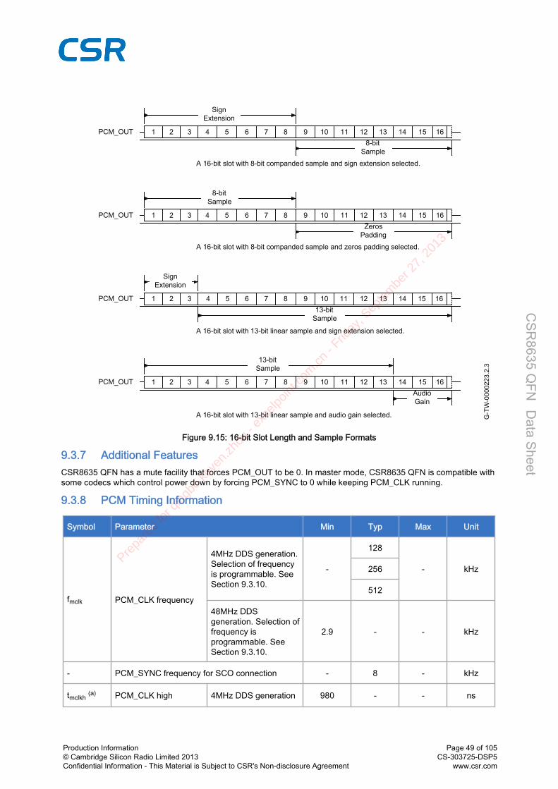
G-T
W-0
0002
23.2
.3
PCM_OUT
PCM_OUT
PCM_OUT
PCM_OUT
1 2 3 4 5 6 7 8 9 10 11 12 13 14 15 16
1 2 3 4 5 6 7 8 9 10 11 12 13 14 15 16
1 2 3 4 5 6 7 8 9 10 11 12 13 14 15 16
1 2 3 4 5 6 7 8 9 10 11 12 13 14 15 16
Sign Extension
8-bit Sample
8-bit Sample
Zeros Padding
Sign Extension
13-bit Sample
13-bit Sample
Audio Gain
A 16-bit slot with 8-bit companded sample and sign extension selected.
A 16-bit slot with 8-bit companded sample and zeros padding selected.
A 16-bit slot with 13-bit linear sample and sign extension selected.
A 16-bit slot with 13-bit linear sample and audio gain selected.
Figure 9.15: 16-bit Slot Length and Sample Formats
9.3.7 Additional FeaturesCSR8635 QFN has a mute facility that forces PCM_OUT to be 0. In master mode, CSR8635 QFN is compatible withsome codecs which control power down by forcing PCM_SYNC to 0 while keeping PCM_CLK running.
9.3.8 PCM Timing Information
Symbol Parameter Min Typ Max Unit
fmclk PCM_CLK frequency
4MHz DDS generation.Selection of frequencyis programmable. SeeSection 9.3.10.
-
128
- kHz256
512
48MHz DDSgeneration. Selection offrequency isprogrammable. SeeSection 9.3.10.
2.9 - - kHz
- PCM_SYNC frequency for SCO connection - 8 - kHz
tmclkh (a) PCM_CLK high 4MHz DDS generation 980 - - ns
Production Information© Cambridge Silicon Radio Limited 2013Confidential Information - This Material is Subject to CSR's Non-disclosure Agreement
Page 49 of 105CS-303725-DSP5
www.csr.com
CSR
8635 QFN D
ata Sheet
Prepa
red
for q
ingbo
keve
n.zh
ou -
exce
lpoint
.com
.cn -
Friday
, Sep
tem
ber 2
7, 2
013

Symbol Parameter Min Typ Max Unit
tmclkl (a) PCM_CLK low 4MHz DDS generation 730 - - ns
- PCM_CLK jitter 48MHz DDS generation - - 21 ns pk-pk
tdmclksynchDelay time from PCM_CLK high to PCM_SYNChigh - - 20 ns
tdmclkpoutDelay time from PCM_CLK high to validPCM_OUT - - 20 ns
tdmclklsynclDelay time from PCM_CLK low to PCM_SYNC low(Long Frame Sync only) - - 20 ns
tdmclkhsynclDelay time from PCM_CLK high to PCM_SYNClow - - 20 ns
tdmclklpoutzDelay time from PCM_CLK low to PCM_OUT highimpedance - - 20 ns
tdmclkhpoutzDelay time from PCM_CLK high to PCM_OUT highimpedance - - 20 ns
tsupinclkl Set-up time for PCM_IN valid to PCM_CLK low 20 - - ns
thpinclkl Hold time for PCM_CLK low to PCM_IN invalid 0 - - ns
Table 9.6: PCM Master Timing(a) Assumes normal system clock operation. Figures vary during low-power modes, when system clock speeds are reduced.
G-T
W-0
0002
24.2
.3PCM_SYNC
PCM_CLK
PCM_OUT
PCM_IN
MSB (LSB) LSB (MSB)
MSB (LSB) LSB (MSB)
fmlk
tmclkh
tmclkl
tsupinclkl
tdmclksynch
tdmclkpout
thpinclkl
tdmclklsyncl
tdmclkhsyncl
tdmclklpoutz
tdmclkhpoutz
tr,t
f
Figure 9.16: PCM Master Timing Long Frame Sync
Production Information© Cambridge Silicon Radio Limited 2013Confidential Information - This Material is Subject to CSR's Non-disclosure Agreement
Page 50 of 105CS-303725-DSP5
www.csr.com
CSR
8635 QFN D
ata Sheet
Prepa
red
for q
ingbo
keve
n.zh
ou -
exce
lpoint
.com
.cn -
Friday
, Sep
tem
ber 2
7, 2
013

G-T
W-0
0002
25.3
.3
PCM_SYNC
PCM_CLK
PCM_OUT
PCM_IN
MSB (LSB) LSB (MSB)
MSB (LSB) LSB (MSB)
fmlk
tmclkh
tmclkl
tsupinclkl
t
tdmclkpout
thpinclkl
dmclkhsyncl
tdmclklpoutz
tdmclkhpoutz
tr,t
f
tdmclksynch
Figure 9.17: PCM Master Timing Short Frame Sync
Production Information© Cambridge Silicon Radio Limited 2013Confidential Information - This Material is Subject to CSR's Non-disclosure Agreement
Page 51 of 105CS-303725-DSP5
www.csr.com
CSR
8635 QFN D
ata Sheet
Prepa
red
for q
ingbo
keve
n.zh
ou -
exce
lpoint
.com
.cn -
Friday
, Sep
tem
ber 2
7, 2
013
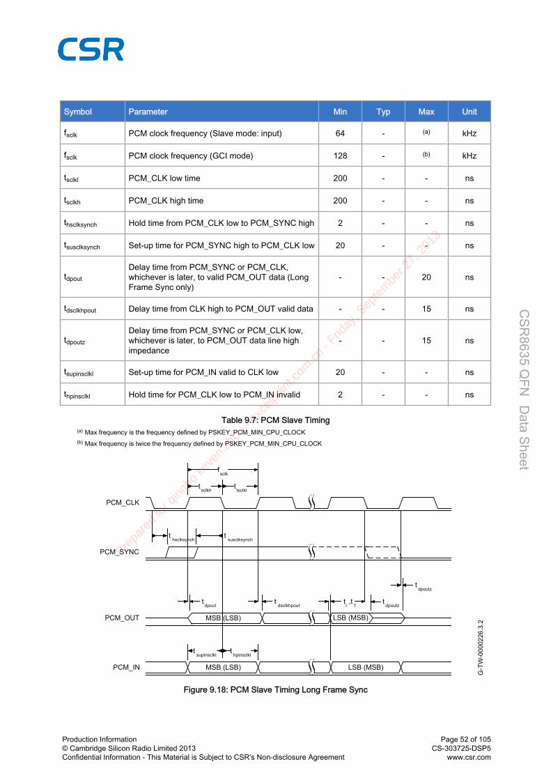
Symbol Parameter Min Typ Max Unit
fsclk PCM clock frequency (Slave mode: input) 64 - (a) kHz
fsclk PCM clock frequency (GCI mode) 128 - (b) kHz
tsclkl PCM_CLK low time 200 - - ns
tsclkh PCM_CLK high time 200 - - ns
thsclksynch Hold time from PCM_CLK low to PCM_SYNC high 2 - - ns
tsusclksynch Set-up time for PCM_SYNC high to PCM_CLK low 20 - - ns
tdpoutDelay time from PCM_SYNC or PCM_CLK,whichever is later, to valid PCM_OUT data (LongFrame Sync only)
- - 20 ns
tdsclkhpout Delay time from CLK high to PCM_OUT valid data - - 15 ns
tdpoutzDelay time from PCM_SYNC or PCM_CLK low,whichever is later, to PCM_OUT data line highimpedance
- - 15 ns
tsupinsclkl Set-up time for PCM_IN valid to CLK low 20 - - ns
thpinsclkl Hold time for PCM_CLK low to PCM_IN invalid 2 - - ns
Table 9.7: PCM Slave Timing(a) Max frequency is the frequency defined by PSKEY_PCM_MIN_CPU_CLOCK(b) Max frequency is twice the frequency defined by PSKEY_PCM_MIN_CPU_CLOCK
G-T
W-0
0002
26.3
.2
PCM_CLK
PCM_SYNC
PCM_OUT
PCM_IN MSB (LSB) LSB (MSB)
fsclk
tsclkh
ttsclkl
thsclksynch
tsusclksynch
tdpout
tdsclkhpout
tdpoutz
tdpoutz
tsupinsclkl
thpinsclkl
tr,t
f
LSB (MSB)MSB (LSB)
Figure 9.18: PCM Slave Timing Long Frame Sync
Production Information© Cambridge Silicon Radio Limited 2013Confidential Information - This Material is Subject to CSR's Non-disclosure Agreement
Page 52 of 105CS-303725-DSP5
www.csr.com
CSR
8635 QFN D
ata Sheet
Prepa
red
for q
ingbo
keve
n.zh
ou -
exce
lpoint
.com
.cn -
Friday
, Sep
tem
ber 2
7, 2
013

G-T
W-0
0002
27.3
.2
PCM_CLK
PCM_SYNC
PCM_OUT
PCM_IN MSB (LSB) LSB (MSB)
fsclk
tsclkh
ttsclkl
thsclksynch
tsusclksynch
tdpoutz
tdpoutz
tsupinsclkl
thpinsclkl
tr,t
f
LSB (MSB)MSB (LSB)
tdsclkhpout
Figure 9.19: PCM Slave Timing Short Frame Sync
9.3.9 PCM_CLK and PCM_SYNC GenerationCSR8635 QFN has 2 methods of generating PCM_CLK and PCM_SYNC in master mode:
Generating these signals by DDS from CSR8635 QFN internal 4MHz clock. Using this mode limits PCM_CLKto 128, 256 or 512kHz and PCM_SYNC to 8kHz.
Generating these signals by DDS from an internal 48MHz clock, which enables a greater range of frequenciesto be generated with low jitter but consumes more power. To select this second method set bit48M_PCM_CLK_GEN_EN in PSKEY_PCM_CONFIG32. When in this mode and with long frame sync, thelength of PCM_SYNC is either 8 or 16 cycles of PCM_CLK, determined by LONG_LENGTH_SYNC_EN inPSKEY_PCM_CONFIG32.
PSKEY_PCM_USE_LOW_JITTER_MODE sets the low jitter mode when the sync rate is 8kHz and the PCM clock isset either by PSKEY_PCM_CLOCK_RATE or through the audio API, see BlueCore Audio API Specification.
9.3.10 PCM ConfigurationConfigure the PCM by using the PS Key PSKEY_PCM_CONFIG32 or through the audio API, see BlueCore Audio APISpecification. The default for PSKEY_PCM_CONFIG32 is 0x00800000, i.e. first slot following sync is active, 13-bitlinear voice format, long frame sync and interface master generating 256kHz PCM_CLK from 4MHz internal clock withno tristate of PCM_OUT.
9.4 Digital Audio Interface (I²S)Important Note:
The I²S interface is provided as a test interface and is only accessible when running the CSR8635 QFN in HCI-only mode.
The digital audio interface supports the industry standard formats for I²S, left-justified or right-justified. The interfaceshares the same pins as the PCM interface, which means each audio bus is mutually exclusive in its usage. Table9.8 lists these alternative functions. Figure 9.20 shows the timing diagram.
Production Information© Cambridge Silicon Radio Limited 2013Confidential Information - This Material is Subject to CSR's Non-disclosure Agreement
Page 53 of 105CS-303725-DSP5
www.csr.com
CSR
8635 QFN D
ata Sheet
Prepa
red
for q
ingbo
keve
n.zh
ou -
exce
lpoint
.com
.cn -
Friday
, Sep
tem
ber 2
7, 2
013

PCM Interface I²S Interface
PCM_OUT SD_OUT
PCM_IN SD_IN
PCM_SYNC WS
PCM_CLK SCK
Table 9.8: Alternative Functions of the Digital Audio Bus Interface on the PCM Interface
Configure the digital audio interface using PSKEY_DIGITAL_AUDIO_CONFIG, see and the PS Key file.
G-T
W-0
0002
30.3
.2
WS
SCK
SD_IN/OUT
WS
SCK
SD_IN/OUT
WS
SCK
SD_IN/OUT
LSB
MSB LSB MSB LSB
MSB LSB MSB LSB
Left -justified Mode
Right -justified Mode
Left Channel Right Channel
Right ChannelLeft Channel
Left Channel Right Channel
MSB LSB MSB
I2 S Mode
Figure 9.20: Digital Audio Interface Modes
The internal representation of audio samples within CSR8635 QFN is 16-bit and data on SD_OUT is limited to 16-bitper channel.
Production Information© Cambridge Silicon Radio Limited 2013Confidential Information - This Material is Subject to CSR's Non-disclosure Agreement
Page 54 of 105CS-303725-DSP5
www.csr.com
CSR
8635 QFN D
ata Sheet
Prepa
red
for q
ingbo
keve
n.zh
ou -
exce
lpoint
.com
.cn -
Friday
, Sep
tem
ber 2
7, 2
013

Symbol Parameter Min Typ Max Unit
- SCK Frequency - - 6.2 MHz
- WS Frequency - - 96 kHz
tch SCK high time 80 - - ns
tcl SCK low time 80 - - ns
Table 9.9: Digital Audio Interface Slave Timing
Symbol Parameter Min Typ Max Unit
tssuWS valid to SCK high set-uptime 20 - - ns
tsh SCK high to WS invalid hold time 2.5 - - ns
topdSCK low to SD_OUT valid delaytime - - 20 ns
tisuSD_IN valid to SCK high set-uptime 20 - - ns
tihSCK high to SD_IN invalid holdtime 2.5 - - ns
Table 9.10: I²S Slave Mode Timing
G-T
W-0
0002
31.2
.2
SD_OUT
SD_IN
t
t
t
t
t
t
WS(Input)
SCK(Input)
ch
opd
ih
shssu
cl
isut
Figure 9.21: Digital Audio Interface Slave Timing
Production Information© Cambridge Silicon Radio Limited 2013Confidential Information - This Material is Subject to CSR's Non-disclosure Agreement
Page 55 of 105CS-303725-DSP5
www.csr.com
CSR
8635 QFN D
ata Sheet
Prepa
red
for q
ingbo
keve
n.zh
ou -
exce
lpoint
.com
.cn -
Friday
, Sep
tem
ber 2
7, 2
013

Symbol Parameter Min Typ Max Unit
- SCK Frequency - - 6.2 MHz
- WS Frequency - - 96 kHz
Table 9.11: Digital Audio Interface Master Timing
Symbol Parameter Min Typ Max Unit
tspd SCK low to WS valid delay time - - 39.27 ns
topdSCK low to SD_OUT valid delaytime - - 18.44 ns
tisuSD_IN valid to SCK high set-uptime 18.44 - - ns
tihSCK high to SD_IN invalid holdtime 0 - - ns
Table 9.12: I²S Master Mode Timing Parameters, WS and SCK as Outputs
G-T
W-0
0002
32.2
.2
WS(Output)
SCK(Output)
SD_OUT
SD_IN
t isu t ih
topd
t spd
Figure 9.22: Digital Audio Interface Master Timing
Production Information© Cambridge Silicon Radio Limited 2013Confidential Information - This Material is Subject to CSR's Non-disclosure Agreement
Page 56 of 105CS-303725-DSP5
www.csr.com
CSR
8635 QFN D
ata Sheet
Prepa
red
for q
ingbo
keve
n.zh
ou -
exce
lpoint
.com
.cn -
Friday
, Sep
tem
ber 2
7, 2
013

10 Power Control and RegulationFor greater power efficiency the CSR8635 QFN contains 2 switch-mode regulators:
1 generates a 1.80V supply rail with an output current of 185mA, see Section 10.1. 1 generates a 1.35V supply rail with an output current of 160mA, see Section 10.2. Combining the 2 switch-mode regulators in parallel generates a single 1.80V supply rail with an output current
of 340mA, see Section 10.3.CSR8635 QFN contains 4 LDO linear regulators:
3.30V bypass regulator, see Section 10.4. 0.85V to 1.20V VDD_DIG linear regulator, see Section 10.5. 1.35V VDD_AUX linear regulator, see Section 10.6. 1.35V VDD_ANA linear regulator, see Section 10.7.
The recommended configurations for power control and regulation on the CSR8635 QFN are: 3 switch-mode configurations:
A 1.80V and 1.35V dual-supply rail system using the 1.80V and 1.35V switch-mode regulators, see Figure10.1. This is the default power control and regulation configuration for the CSR8635 QFN.
A 1.80V single-supply rail system using the 1.80V switch-mode regulator. A 1.80V parallel-supply rail system for higher currents using the 1.80V and 1.35V switch-mode regulators
with combined outputs, see Figure 10.2. A linear configuration using an external 1.8V rail omitting all regulators
Table 10.1 shows settings for the recommended configurations for power control and regulation on the CSR8635 QFN.
SupplyConfiguration
RegulatorsSupply Rail
Switch-mode VDD_AUXLinear
Regulator
VDD_ANALinear
Regulator1.8V 1.35V 1.8V 1.35V
Dual-supplySMPS ON ON OFF OFF SMPS SMPS
Single-supplySMPS ON OFF ON ON SMPS LDO
Parallel-supply SMPS ON ON ON ON SMPS LDO
Linear supply OFF OFF ON ON External LDO
Table 10.1: Recommended Configurations for Power Control and Regulation
For more information on CSR8635 QFN power supply configuration see the Configuring the Power Supplies onCSR8670 application note.
Production Information© Cambridge Silicon Radio Limited 2013Confidential Information - This Material is Subject to CSR's Non-disclosure Agreement
Page 57 of 105CS-303725-DSP5
www.csr.com
CSR
8635 QFN D
ata Sheet
Prepa
red
for q
ingbo
keve
n.zh
ou -
exce
lpoint
.com
.cn -
Friday
, Sep
tem
ber 2
7, 2
013
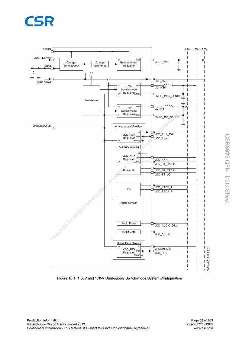
G-T
W-0
0121
82.2
.2
Charge Reference
Bypass Linear Regulator
Charger50 to 200mA
Reference
1.8V Switch-mode
Regulator
1.35V Switch-mode
Regulator
VCHG
VBAT
VBAT_SENSE
LX_1V35
LX_1V8
VOUT_3V3
3.3V1.35V1.8V
Audio Driver
Audio Core
VDD_AUDIO_DRV
VDD_AUDIO
Audio Circuits
VDD_AUX Regulator
VDD_ANA Regulator
I/O
Analogue and Auxiliary
Bluetooth
SMPS_1V8_SENSE
SMPS_1V35_SENSE
SENSE
IN
OUT
OUT
VDD_AUX
SENSE
OUT
OUT
VDD_ANASENSE
IN
SENSE
Auxiliary Circuits
IN
IN
Digital Core Circuits
VDD_DIGRegulator
OUT
SENSE
IN
VDD_DIGVREGIN_DIG
EN
EN
EN
EN
EN
EN OUT
VREGENABLE
VDD_PADS_1VDD_PADS_2
VDD_AUX_1V8
VDD_BT_RADIOVDD_BT_LO
VDD_BT_RADIO
SMP_VBAT SMP_BYP
Figure 10.1: 1.80V and 1.35V Dual-supply Switch-mode System Configuration
Production Information© Cambridge Silicon Radio Limited 2013Confidential Information - This Material is Subject to CSR's Non-disclosure Agreement
Page 58 of 105CS-303725-DSP5
www.csr.com
CSR
8635 QFN D
ata Sheet
Prepa
red
for q
ingbo
keve
n.zh
ou -
exce
lpoint
.com
.cn -
Friday
, Sep
tem
ber 2
7, 2
013

G-T
W-0
0121
83.2
.2
Charge Reference
Bypass Linear Regulator
Charger50 to 200mA
Reference
1.8V Switch-mode
Regulator
1.35V Switch-mode
Regulator
VCHG
LX_1V35
LX_1V8
VOUT_3V3
3.3V1.35V1.8V
Audio Driver
Audio Core
VDD_AUDIO_DRV
VDD_AUDIO
Audio Circuits
VDD_AUX Regulator
VDD_ANA Regulator
I/O
Analogue and Auxiliary
Bluetooth
SMPS_1V8_SENSE
SMPS_1V35_SENSE
SENSE
IN
OUT
OUT
VDD_AUX
SENSE
OUT
OUT
VDD_ANASENSE
IN
SENSE
Auxiliary Circuits
IN
IN
Digital Core Circuits
VDD_DIGRegulator
OUT
SENSE
IN
VDD_DIGVREGIN_DIG
EN
EN
EN
EN
EN
EN OUT
VREGENABLE
VDD_PADS_1VDD_PADS_2
VDD_AUX_1V8
VDD_BT_RADIOVDD_BT_LO
VDD_BT_RADIO
VBAT
VBAT_SENSE
SMP_VBAT SMP_BYP
Figure 10.2: 1.80V Parallel-supply Switch-mode System Configuration
10.1 1.8V Switch-mode RegulatorCSR recommends using the integrated switch-mode regulator to power the 1.80V supply rail.
Production Information© Cambridge Silicon Radio Limited 2013Confidential Information - This Material is Subject to CSR's Non-disclosure Agreement
Page 59 of 105CS-303725-DSP5
www.csr.com
CSR
8635 QFN D
ata Sheet
Prepa
red
for q
ingbo
keve
n.zh
ou -
exce
lpoint
.com
.cn -
Friday
, Sep
tem
ber 2
7, 2
013
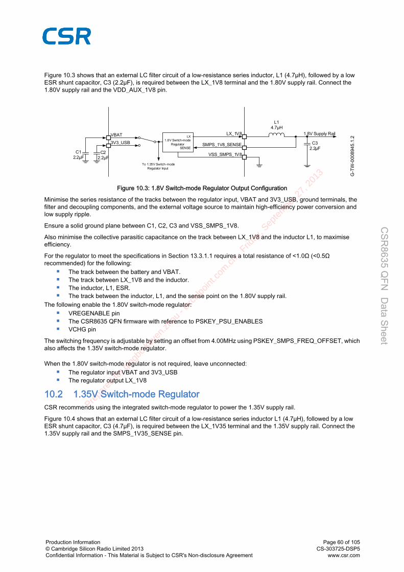
Figure 10.3 shows that an external LC filter circuit of a low-resistance series inductor, L1 (4.7µH), followed by a lowESR shunt capacitor, C3 (2.2µF), is required between the LX_1V8 terminal and the 1.80V supply rail. Connect the1.80V supply rail and the VDD_AUX_1V8 pin.
G-T
W-0
0089
45.1
.2
SMPS_1V8_SENSE
LX_1V81.8V Switch-mode
RegulatorSENSE
LX
L14.7µH
C32.2µF
1.8V Supply Rail
VSS_SMPS_1V8
VBAT3V3_USB
To 1.35V Switch-mode Regulator Input
C12.2µF
C22.2µF
Figure 10.3: 1.8V Switch-mode Regulator Output Configuration
Minimise the series resistance of the tracks between the regulator input, VBAT and 3V3_USB, ground terminals, thefilter and decoupling components, and the external voltage source to maintain high-efficiency power conversion andlow supply ripple.
Ensure a solid ground plane between C1, C2, C3 and VSS_SMPS_1V8.
Also minimise the collective parasitic capacitance on the track between LX_1V8 and the inductor L1, to maximiseefficiency.
For the regulator to meet the specifications in Section 13.3.1.1 requires a total resistance of <1.0Ω (<0.5Ωrecommended) for the following:
The track between the battery and VBAT. The track between LX_1V8 and the inductor. The inductor, L1, ESR. The track between the inductor, L1, and the sense point on the 1.80V supply rail.
The following enable the 1.80V switch-mode regulator: VREGENABLE pin The CSR8635 QFN firmware with reference to PSKEY_PSU_ENABLES VCHG pin
The switching frequency is adjustable by setting an offset from 4.00MHz using PSKEY_SMPS_FREQ_OFFSET, whichalso affects the 1.35V switch-mode regulator.
When the 1.80V switch-mode regulator is not required, leave unconnected: The regulator input VBAT and 3V3_USB The regulator output LX_1V8
10.2 1.35V Switch-mode RegulatorCSR recommends using the integrated switch-mode regulator to power the 1.35V supply rail.
Figure 10.4 shows that an external LC filter circuit of a low-resistance series inductor L1 (4.7µH), followed by a lowESR shunt capacitor, C3 (4.7µF), is required between the LX_1V35 terminal and the 1.35V supply rail. Connect the1.35V supply rail and the SMPS_1V35_SENSE pin.
Production Information© Cambridge Silicon Radio Limited 2013Confidential Information - This Material is Subject to CSR's Non-disclosure Agreement
Page 60 of 105CS-303725-DSP5
www.csr.com
CSR
8635 QFN D
ata Sheet
Prepa
red
for q
ingbo
keve
n.zh
ou -
exce
lpoint
.com
.cn -
Friday
, Sep
tem
ber 2
7, 2
013

G-T
W-0
0089
46.1
.2
SMPS_1V35_SENSE
LX_1V351.35V Switch-
mode RegulatorSENSE
LX
L14.7µH
C34.7µF
1.35V Supply Rail
VSS_SMPS_1V35
VBAT3V3_USB
To 1.8V Switch-mode Regulator Input
C12.2µF
C22.2µF
Figure 10.4: 1.35V Switch-mode Regulator Output Configuration
Minimise the series resistance of the tracks between the regulator input, VBAT and 3V3_USB, ground terminals, thefilter and decoupling components, and the external voltage source to maintain high-efficiency power conversion andlow supply ripple.
Ensure a solid ground plane between C1, C2, C3 and VSS_SMPS_1V35.
Also minimise the collective parasitic capacitance on the track between LX_1V35 and the inductor L1, to maximiseefficiency.
For the regulator to meet the specifications in Section 13.3.2.1 requires a total resistance of <1.0Ω (<0.5Ωrecommended) for the following:
The track between the battery and VBAT. The track between LX_1V8 and the inductor. The inductor, L1, ESR. The track between the inductor, L1, and the sense point on the 1.35V supply rail.
The following enable the 1.35V switch-mode regulator: VREGENABLE pin The CSR8635 QFN firmware with reference to PSKEY_PSU_ENABLES VCHG pin
The switching frequency is adjustable by setting an offset from 4.00MHz using PSKEY_SMPS_FREQ_OFFSET, whichalso affects the 1.80V switch-mode regulator.
When the 1.35V switch-mode regulator is not required, leave unconnected: The regulator input VBAT and 3V3_USB The regulator output LX_1V35
10.3 1.8V and 1.35V Switch-mode Regulators CombinedFor applications that require a single 1.80V supply rail with higher currents CSR recommends combining the outputsof the integrated 1.80V and 1.35V switch-mode regulators in parallel to power a single 1.80V supply rail, see Figure10.5.
Figure 10.5 shows that an external LC filter circuit of a low-resistance series inductor L1 (4.7µH), followed by a lowESR shunt capacitor, C3 (2.2µF), is required between the LX_1V8 terminal and the 1.80V supply rail. Connect the1.80V supply rail and the VDD_AUX_1V8 pin and ground the SMPS_1V35_SENSE pin.
Production Information© Cambridge Silicon Radio Limited 2013Confidential Information - This Material is Subject to CSR's Non-disclosure Agreement
Page 61 of 105CS-303725-DSP5
www.csr.com
CSR
8635 QFN D
ata Sheet
Prepa
red
for q
ingbo
keve
n.zh
ou -
exce
lpoint
.com
.cn -
Friday
, Sep
tem
ber 2
7, 2
013

G-T
W-0
0089
47.1
.2SMPS_1V8_SENSE
LX_1V81.8V Switch-mode
RegulatorSENSE
LX
L14.7µH
C32.2µF
1.8V Supply Rail
VSS_SMPS_1V8
SMPS_1V35_SENSE
LX_1V351.35V Switch-
mode RegulatorSENSE
LX
VSS_SMPS_1V35
VBAT3V3_USB
C12.2µF
C22.2µF
Figure 10.5: 1.8V and 1.35V Switch-mode Regulators Outputs Parallel Configuration
Minimise the series resistance of the tracks between the regulator input VBAT and 3V3_USB, ground terminals, thefilter and decoupling components, and the external voltage source to maintain high-efficiency power conversion andlow supply ripple.
Ensure a solid ground plane between C1, C2, C3, VSS_SMPS_1V8 and VSS_SMPS_1V35.
Also minimise the collective parasitic capacitance on the track between LX_1V8, LX_1V35 and the inductor L1, tomaximise efficiency.
For the regulator to meet the specifications in Section 13.3.1.2 requires a total resistance of <1.0Ω (<0.5Ωrecommended) for the following:
The track between the battery and VBAT. The track between LX_1V8, LX_1V35 and the inductor. The inductor L1, ESR. The track between the inductor, L1, and the sense point on the 1.80V supply rail.
The following enable the 1.80V switch-mode regulator: VREGENABLE pin The CSR8635 QFN firmware with reference to PSKEY_PSU_ENABLES VCHG pin
The switching frequency is adjustable by setting an offset from 4.00MHz using PSKEY_SMPS_FREQ_OFFSET.
When the 1.80V switch-mode regulator is not required, leave unconnected: The regulator input VBAT and 3V3_USB The regulator output LX_1V8
10.4 Bypass LDO Linear RegulatorThe integrated bypass LDO linear regulator is available as a 3.30V supply rail and is an alternative supply rail to thebattery supply. This is especially useful when the battery has no charge and the CSR8635 QFN needs to power up.The input voltage should be between 4.25V to 6.50V.
Note:
The integrated bypass LDO linear regulator can operate down to 3.1V with a reduced performance.
Externally decouple the output of this regulator using a low ESR MLC capacitor of a minimum 2.2µF to the 3V3_USBpin.
The output voltage is switched on when VCHG gets above 3.0V.
Production Information© Cambridge Silicon Radio Limited 2013Confidential Information - This Material is Subject to CSR's Non-disclosure Agreement
Page 62 of 105CS-303725-DSP5
www.csr.com
CSR
8635 QFN D
ata Sheet
Prepa
red
for q
ingbo
keve
n.zh
ou -
exce
lpoint
.com
.cn -
Friday
, Sep
tem
ber 2
7, 2
013

10.5 Low-voltage VDD_DIG Linear RegulatorThe integrated low-voltage VDD_DIG linear regulator powers the digital circuits on CSR8635 QFN. Externally decouplethe output of this regulator using a low ESR MLC capacitor of 470nF.
10.6 Low-voltage VDD_AUX Linear RegulatorThe integrated low-voltage VDD_AUX linear regulator is optionally available to provide a 1.35V auxiliary supply railwhen the 1.35V switch-mode regulator is not used. When using the integrated low-voltage VDD_AUX linear regulator,externally decouple the output of this regulator using a low ESR MLC capacitor of a minimum 470nF to the VDD_AUXpin.
10.7 Low-voltage VDD_ANA Linear RegulatorThe integrated low-voltage VDD_ANA linear regulator is optionally available to power the 1.35V analogue supply railwhen the 1.35V switch-mode regulator is not used. When using the integrated low-voltage VDD_ANA linear regulator,externally decouple the output of this regulator using a 2.2µF low ESR MLC capacitor to the VDD_ANA pin.
10.8 Voltage Regulator EnableWhen using the integrated regulators the voltage regulator enable pin, VREGENABLE, enables the CSR8635 QFNand the following regulators:
1.8V switch-mode regulator 1.35V switch-mode regulator Low-voltage VDD_DIG linear regulator Low-voltage VDD_AUX linear regulator
The VREGENABLE pin is active high, with a pull-down, typical 100kΩ, which is disabled byPSKEY_VREG_ENABLE_STRONG_PULL.
CSR8635 QFN boots-up when the voltage regulator enable pin is pulled high typically for 10 to 15ms, enabling theregulators. The firmware then latches the regulators on. The voltage regulator enable pin can then be released.
The status of the VREGENABLE pin is available to firmware through an internal connection. VREGENABLE also worksas an input line.
Note:
VREGENABLE should be asserted after the VBAT supply when VREGENABLE is not used as a power-on button.
10.9 External Regulators and Power SequencingCSR recommends that the integrated regulators supply the CSR8635 QFN and it is configured based on the informationin this data sheet.
If any of the supply rails for the CSR8635 QFN are supplied from an external regulator, then it should match or be betterthan the internal regulator available on CSR8635 QFN. For more information see regulator characteristics in Section13.
Note:
The internal regulators described in Section 10.1 to Section 10.7 are not recommended for external circuitry otherthan that shown in Section 12.
For information about power sequencing of external regulators to supply the CSR8635 QFN contact CSR.
10.10 Reset, RST#CSR8635 QFN is reset from several sources:
RST# pin Power-on reset USB charger attach reset Software configured watchdog timer
Production Information© Cambridge Silicon Radio Limited 2013Confidential Information - This Material is Subject to CSR's Non-disclosure Agreement
Page 63 of 105CS-303725-DSP5
www.csr.com
CSR
8635 QFN D
ata Sheet
Prepa
red
for q
ingbo
keve
n.zh
ou -
exce
lpoint
.com
.cn -
Friday
, Sep
tem
ber 2
7, 2
013

The RST# pin is an active low reset and is internally filtered using the internal low frequency clock oscillator. CSRrecommends applying RST# for a period >5ms.
At reset the digital I/O pins are set to inputs for bidirectional pins and outputs are set to tristate.
10.10.1 Digital Pin States on ResetTable 10.2 shows the pin states of CSR8635 QFN on reset.
Pin Name I/O Type Full Chip Reset Pin Name I/O Type Full Chip Reset
USB_DP Digital bidirectional N/A PIO[9] Digital bidirectional PDS
USB_DN Digital bidirectional N/A PIO[10] Digital bidirectional PDS
PIO[0] Digital bidirectional PUS PIO[11] Digital bidirectional PDS
PIO[1] Digital bidirectional PUS PIO[12] Digital bidirectional PUS
PIO[2] Digital bidirectional PDW PIO[13] Digital bidirectional PDS
PIO[3] Digital bidirectional PDW PIO[14] Digital bidirectional PUS
PIO[4] Digital bidirectional PDW PIO[15] Digital bidirectional PUS
PIO[5] Digital bidirectional PDW PIO[16] Digital bidirectional PUS
PIO[6] Digital bidirectional PDS PIO[17] Digital bidirectional PDS
PIO[7] Digital bidirectional PDS PIO[18] Digital bidirectional PDW
PIO[8] Digital bidirectional PUS PIO[21] Digital bidirectional PDW
Table 10.2: Pin States on Reset
Note:
PUS = Strong pull-up
PDS = Strong pull-down
PUW = Weak pull-up
PDW = Weak pull-down
10.10.2 Status After ResetThe status of CSR8635 QFN after a reset is:
Warm reset: baud rate and RAM data remain available Cold reset: baud rate and RAM data not available
10.11 Automatic Reset ProtectionCSR8635 QFN includes an automatic reset protection circuit which restarts/resets CSR8635 QFN when an unexpectedreset occurs, e.g. ESD strike or lowering of RST#. The automatic reset protection circuit enables resets from the VMwithout the requirement for external circuitry.
Note:
The reset protection is cleared after typically 2s (1.6s min to 2.4s max).
If RST# is held low for >2.4s CSR8635 QFN turns off. A rising edge on VREGENABLE or VCHG is required topower on CSR8635 QFN.
Production Information© Cambridge Silicon Radio Limited 2013Confidential Information - This Material is Subject to CSR's Non-disclosure Agreement
Page 64 of 105CS-303725-DSP5
www.csr.com
CSR
8635 QFN D
ata Sheet
Prepa
red
for q
ingbo
keve
n.zh
ou -
exce
lpoint
.com
.cn -
Friday
, Sep
tem
ber 2
7, 2
013

11 Battery Charger11.1 Battery Charger Hardware Operating ModesThe battery charger hardware is controlled by the VM, see Section 11.3.The battery charger has 5 modes:
Disabled Trickle charge Fast charge Standby: fully charged or float charge Error: charging input voltage, VCHG, is too low
The battery charger operating mode is determined by the battery voltage and current, see Table 11.1 and Figure11.1.
The internal charger circuit can provide up to 200mA of charge current, for currents higher than this the CSR8635 QFNcan control an external pass transistor, see Section 11.5.
Mode Battery Charger Enabled VBAT_SENSE
Disabled No X
Trickle charge Yes >0 and <Vfast
Fast charge Yes >Vfast and <Vfloat
Standby Yes Iterm (a) and >(Vfloat - Vhyst)
Error Yes >(VCHG - 50mV)
Table 11.1: Battery Charger Operating Modes Determined by Battery Voltage and Current(a) Iterm is approximately 10% of Ifast for a given Ifast setting
Figure 11.1 shows the mode-to-mode transition voltages. These voltages are fixed and calibrated by CSR, see Section11.2. The transition between modes can occur at any time.
G-T
W-0
0055
83.3
.2
Battery Voltage
Cha
rge
Cur
rent
Vfast
Ifast
ItermVhystItrickle
Vfloat
Trickle Charge Mode
Fast Charge ModeConstant Current
Fast Charge ModeConstant Voltage
Standby Mode
Figure 11.1: Battery Charger Mode-to-Mode Transition Diagram
Production Information© Cambridge Silicon Radio Limited 2013Confidential Information - This Material is Subject to CSR's Non-disclosure Agreement
Page 65 of 105CS-303725-DSP5
www.csr.com
CSR
8635 QFN D
ata Sheet
Prepa
red
for q
ingbo
keve
n.zh
ou -
exce
lpoint
.com
.cn -
Friday
, Sep
tem
ber 2
7, 2
013

Note:
The battery voltage remains constant in Fast Charge Constant Voltage Mode, the curved line on Figure 11.1 is forclarity only.
11.1.1 Disabled ModeIn the disabled mode the battery charger is fully disabled and draws no active current on any of its terminals.
11.1.2 Trickle Charge ModeIn the trickle charge mode, when the voltage on VBAT_SENSE is lower than the Vfast threshold, a current ofapproximately 10% of the fast charge current, Ifast, is sourced from the VBAT pin.
The Vfast threshold detection has hysteresis to prevent the charger from oscillating between modes.
11.1.3 Fast Charge ModeWhen the voltage on VBAT_SENSE is greater than Vfast, the current sourced from the VBAT pin increases to Ifast.Ifast is between 10mA and 200mA set by PS Key or a VM trap. In addition, Ifast is calibrated in production test to correctfor process variation in the charger circuit.
The current is held constant at Ifast until the voltage at VBAT_SENSE reaches Vfloat, then the charger reduces the currentsourced to maintain a constant voltage on the VBAT_SENSE pin.
When the current sourced is below the termination current, Iterm, the charging stops and the charger enters standbymode. Iterm is typically 10% of the fast charge current.
11.1.4 Standby ModeWhen the battery is fully charged, the charger enters standby mode, and battery charging stops. The battery voltageon the VBAT_SENSE pin is monitored, and when it drops below a threshold set at Vhyst below the final charging voltage,Vfloat, the charger re-enters fast charge mode.
11.1.5 Error ModeThe charger enters the error mode if the voltage on the VCHG pin is too low to operate the charger correctly(VBAT_SENSE is greater than VCHG - 50mV (typical)).
In this mode, charging is stopped. The battery charger does not require a reset to resume normal operation.
11.2 Battery Charger Trimming and CalibrationThe battery charger default trim values are written by CSR into non-volatile memory when each IC is characterised.CSR provides various PS Keys for overriding the default trims, see Section 11.4.
11.3 VM Battery Charger ControlThe VM charger code has overall supervisory control of the battery charger and is responsible for:
Responding to charger power connection/disconnection events Monitoring the temperature of the battery Monitoring the temperature of the die to protect against silicon damage Monitoring the time spent in the various charge states Enabling/disabling the charger circuitry based on the monitored information Driving the user visible charger status LED(s)
11.4 Battery Charger Firmware and PS KeysThe battery charger firmware sets up the charger hardware based on the PS Key settings and traps called from theVM charger code. It also performs the initial analogue trimming. Settings for the charger current depend on the batterycapacity and type, which are set by the user in the PS Keys.
For more information on the CSR8635 QFN, including details on setting up, calibrating, trimming and the PS Keys, seeLithium Polymer Battery Charger Calibration and Operation for CSR8670 application note.
Production Information© Cambridge Silicon Radio Limited 2013Confidential Information - This Material is Subject to CSR's Non-disclosure Agreement
Page 66 of 105CS-303725-DSP5
www.csr.com
CSR
8635 QFN D
ata Sheet
Prepa
red
for q
ingbo
keve
n.zh
ou -
exce
lpoint
.com
.cn -
Friday
, Sep
tem
ber 2
7, 2
013

11.5 External ModeThe external mode is for charging higher capacity batteries using an external pass device. The current is controlled bysinking a varying current into the CHG_EXT pin, and the current is determined by measuring the voltage drop acrossa resistor, Rsense, connected in series with the external pass device, see Figure 11.2. The voltage drop is determinedby looking at the difference between the VBAT_SENSE and VBAT pins. The voltage drop across Rsense is typically200mV. The value of the external series resistor determines the charger current. This current can be trimmed with aPS Key.
In Figure 11.2, R1 (220mΩ) and C1 (4.7µF) form an RC snubber that is required to maintain stability across all batteryESRs. The battery ESR must be <1.0Ω.
G-T
W-0
0055
85.2
.3
VCHG
CHG_EXT
VBAT_SENSE
VBAT
BAT 1 Li+ Cell
Rsense
TR 1External Pass Device
R1220mΩ
C14.7µF
Figure 11.2: Battery Charger External Mode Typical Configuration
Production Information© Cambridge Silicon Radio Limited 2013Confidential Information - This Material is Subject to CSR's Non-disclosure Agreement
Page 67 of 105CS-303725-DSP5
www.csr.com
CSR
8635 QFN D
ata Sheet
Prepa
red
for q
ingbo
keve
n.zh
ou -
exce
lpoint
.com
.cn -
Friday
, Sep
tem
ber 2
7, 2
013

12 Example Application Schematic
G-T
W-0
0129
57.3
.3
26MHzXT1
GR
EE
N
D103
Li+ CELL
VBAT
3.7VCON101
1V8
VBAT
1V81V8
F2S102
F3S101
F4S100
RE
D
D102
BLU
E
D101
1V81V8
VOL-S104
VOL+S103
LED
_0
LED
_1
LED
_2
LED outputs
VBUS
GND 5ID 4D+ 3D- 2VBUS 1
GN
D6
GN
D7
USB MINI-BCON100
USB_PUSB_N3
1
2
BCX51Q100
VBUS
1%400mR
R104
CHG_EXT
VBAT_SENSE
VBAT
BAT54CD100
VBUS
VBATVBUS 3V3_USBVBAT 1V8_SMPS
MFBS1
4u7L2
1V35_SMPS 1V8_SMPS
STARSP100
CE 1SO/SIO12WP/SIO23
VSS 4
SI/SIO05SCK 6
HOLD/SIO37
VDD8U100
SPI Flash
1V8_SMPS
PIO_0
LED_1LED_0
PIO_1
PIO_2PIO_3PIO_4PIO_5
PIO_6PIO_7PIO_8PIO_9
AIO_0
USB_PUSB_N
SPI_PCM#
LED_2
PIO_12
PIO_13
PIO_10PIO_11
JACK_DET_PIOLINE/MIC_PIOPIO_16PIO_17
PIO_18PIO_21
i50R
i50R
FR_TBTNA
CH
G_E
XT
VB
AT_S
EN
SE
OUT2 IN 4
GND 1GND3
2.45GHz
U2
RSTB
2u2C1
2u2C2
2u2C3
2u2C4
10nC5
10nC6
470nC10
15pC8
10nC101
PIO / UART
PIO / PCM1 / Debug SPI / I2S
PIO / Serial Flash / I2C
Analogue Input / Output
USB (12Mbps)
Reset
Bluetooth RF
Optional Ancilliary CircuitsOptional Fast charge400mohm = 500mA
USB / Charger Interface Lithium Polymer Battery(battery protection built in)
Typical LED's and ButtonsOptional 1x SPI FLASH memory
Connect VBAT_SENSE to VBATif not using this circuit
Ensure the following tracks have good low impedance connections
PCB Layout Notes
(no via share and short thick tracks)VSS_SMPS_1V8 to Battery GroundVSS_SMPS_1V35 to Battery Ground
LX_1V8 to InductorLX_1V35 to Inductor
L1 to C4 trackL2 to C7 track
VBAT to Battery and C2 - should be <1ohm from batteryVCHG to charger connector and C1
VDD_DIG to Ground
Suggest analogue and digital grounds are separated if possible
and star connected near VSS_AUDIO as shown
CSR recommend low Rdc inductors (<0.5R) for L1 & L2 for optimum power efficiencyFor example Taiyo Yuden CB2012T4R7M
4u7L1
Ensure analogue tracks stay over Analogue ground as much as possible
220RR101
330RR102
330RR103
PIO_12PIO_10
PIO_11PIO_13
PIO
_n
PIO
_n
PIO
_n
PIO
_n
PIO
_n
4u7C105
220mRR108
Ensure the following components are placed next to CSR8635 QFNand have good low impedance connections both to signal and GND
C2 and C3
1V8_SMPS
C4 to VSS_SMPS_1V8C7 to VSS_SMPS_1V35
SPI/PCM# high for SPI. Low for all other functions
Ensure good low impedance ground return path through GND plane for SMPSUcurrent from C4 to VSS_SMPS_1V8 and C7 to VSS_SMPS_1V35 back to C3 & C4
1V8_SMPS
10n
C100
Optional I2C EEPROM memory
PIO_11PIO_10
24AAxxx
VCC8
VSS 4A2 3SCL6 A1 2A0 1WP7
SDA5
U101
PIO_12
2k2R107
2k2R106
2k2R105
Size of EEPROM depends on voice prompt requirements
2u2C9
4u7C7
Ensure routing from L2 to pin 39 and from L2 to C8/9 & pins 11 & 13 are kept separate
100nC11
PIO / LINE-MIC Select / Jack Detect
10kTHERM
AIO_0
Battery temperature sensor
9k1
R1001V35_SMPS
10nC102
S
D
G
Q1
PIO_n
LIN
E/M
IC_A
N
LIN
E/M
IC_A
P
LIN
E_B
P
LIN
E_B
N
MIC
_BIA
S
SP
KR
_LN
SP
KR
_LP
SPK
R_R
NS
PKR
_RP
Speakers (16-32 Ohm)Left Right
2u2C12
SM
P_B
YP
49
VD
D_A
UD
IO3
VD
D_D
IG38
VD
D_P
ADS_
133
BT_RF12
CSR8635 QFN
VD
D_A
NA
17
VDD
_AU
X14
VD
D_P
ADS_
263
VREG
EN
AB
LE40
VC
HG
42
VBA
T45
LX_1
V847
BYPASS REG
CHARGER
DIG LDO
AUX LDO
ANA LDO
VS
S_S
MP
S_1
V35
51
3V3
1V35
1V35
VR
EG
IN_D
IG39
VBAT 1V8 SMPS
1V35 SMPS
LX_1
V35
50
SMPS
_1V3
5_S
EN
SE52
VD
D_A
UX
_1V
815
1V35
VS
S_S
MP
S_1
V846
PIO[6] 62
RST# 35
XTAL_IN 19
XTAL_OUT 18
AIO[0] 20
PIO[30] / LED[1] 36PIO[29] / LED[0] 37
PIO[31] / LED[2] 66
USB_P 56USB_N 55
PIO[12] / QSPI_FLASH_CS# / I2C_WP 22
PIO[14] / UART_RX 23PIO[15] / UART_TX 21
PIO[16] / UART_RTS# 27PIO[17] / UART_CTS# 32
PIO[11] / QSPI_IO[0] / I2C_SDA 26
PIO[13] / QSPI_IO[1] 31
VD
D_A
UD
IO_D
RV
8
GN
D P
ADD
LE69
PIO[10] / QSPI_FLASH_CLK / I2C_SCL 25
CH
G_E
XT
43
VBA
T_S
ENS
E44
PIO[18] 65
PIO[4] / PCM1_SYNC / SPI_CS# 24PIO[5] / PCM1_CLK / SPI_CLK 34
SPI_PCM# 29
PIO[2] / PCM1_IN / SPI_MOSI 30PIO[3] / PCM1_OUT / SPI_MISO 28
PIO[7] 57
SM
PS
_1V8
_SEN
SE53
PIO[9] / UART_CTS# 58
PIO[1] / UART_TX 60
PIO[8] / UART_RTS# 61
PIO[0] / UART_RX 59
PIO[21] 64
VD
D_A
UX
_1V
816
VDD
_BT_
LO13
VD
D_B
T_R
AD
IO11
VO
UT_
3V3
41
SM
P_V
BAT
48
VDD
_US
B54
MIC
_BIA
S2
AU
_RE
F1
MIC BIAS
SP
KR_R
N6
SP
KR_R
P7
SP
KR_L
N9
SP
KR_L
P10
LIN
E/M
IC_A
P68
LIN
E/M
IC_A
N67
LIN
E_B
P5
LIN
E_B
N4
15nH
L4Mic1
15pC17 2k2
R2100nC15
100nC16
MIC_N
MIC_P
MIC_BIAS
STX-3100-9N
SHIELD 1R 2
L 5
678
91011
UNMATED
UNMATED
MATED
MATED
CON1
Line Jack
GN
DV
+
U1
1V82u2C142u2C13
LINE/MIC_AN
LINE/MIC_AP
2u2C19
LINE/MIC_PIO
Analogue 2xSPDT Switcheg MAX4717 / TS3A24157 or alternatives
LINE_BP
2u2C18
LINE_BN
JACK_DET_PIO
Line Input / Microphone Auto Switch Circuit
LINE_L
Figure 12.1: Single Microphone and Stereo Line Input
Production Information© Cambridge Silicon Radio Limited 2013Confidential Information - This Material is Subject to CSR's Non-disclosure Agreement
Page 68 of 105CS-303725-DSP5
www.csr.com
CSR
8635 QFN D
ata Sheet
Prepa
red
for q
ingbo
keve
n.zh
ou -
exce
lpoint
.com
.cn -
Friday
, Sep
tem
ber 2
7, 2
013

G-T
W-0
0129
77.2
.3
26MHzXT1
GR
EE
N
D103
Li+ CELL
VBAT
3.7VCON101
1V8
VBAT
1V81V8
F2S102
F3S101
F4S100
RE
D
D102
BLU
E
D101
1V81V8
VOL-S104
VOL+S103
LED
_0
LED
_1
LED
_2
LED outputs
VBUS
GND 5ID 4D+ 3D- 2VBUS 1
GN
D6
GN
D7
USB MINI-BCON100
USB_PUSB_N3
1
2
BCX51Q100
VBUS
1%400mR
R104
CHG_EXT
VBAT_SENSE
VBAT
BAT54CD100
VBUS
VBATVBUS 3V3_USBVBAT 1V8_SMPS
MFBS1
4u7L2
1V35_SMPS 1V8_SMPS
STARSP100
CE 1
SO/SIO12
WP/SIO23
VSS 4
SI/SIO05
SCK 6
HOLD/SIO37
VDD8U100
SPI Flash
1V8_SMPS
PIO_0
LED_1LED_0
PIO_1
PIO_2PIO_3PIO_4PIO_5
PIO_6PIO_7PIO_8PIO_9
AIO_0
USB_PUSB_N
SPI_PCM#
LED_2
PIO_12
PIO_13
PIO_10PIO_11
PIO_14PIO_15PIO_16PIO_17
PIO_18PIO_21
i50R
i50R
FR_TBTNA
CH
G_E
XT
VBA
T_S
EN
SE
OUT2 IN 4
GND 1GND3
2.45GHz
U2
RSTB
2u2C1
2u2C2
2u2C3
2u2C4
10nC5
10nC6
470nC10
15pC8
10nC101
PIO / UART
PIO / PCM1 / Debug SPI / I2S
PIO / Serial Flash / I2C
Analogue Input / Output
USB (12Mbps)
Reset
Bluetooth RF
Optional Ancilliary CircuitsOptional Fast charge400mohm = 500mA
USB / Charger Interface Lithium Polymer Battery(battery protection built in)
Typical LED's and ButtonsOptional 1x SPI FLASH memory
Connect VBAT_SENSE to VBATif not using this circuit
Ensure the following tracks have good low impedance connections
PCB Layout Notes
(no via share and short thick tracks)VSS_SMPS_1V8 to Battery GroundVSS_SMPS_1V35 to Battery Ground
LX_1V8 to InductorLX_1V35 to Inductor
L1 to C4 trackL2 to C7 track
VBAT to Battery and C2 - should be <1ohm from batteryVCHG to charger connector and C1
VDD_DIG to Ground
Suggest analogue and digital grounds are separated if possible
and star connected near VSS_AUDIO as shown
CSR recommend low Rdc inductors (<0.5R) for L1 & L2 for optimum power efficiencyFor example Taiyo Yuden CB2012T4R7M
4u7L1
Ensure analogue tracks stay over Analogue ground as much as possible
220RR101
330RR102
330RR103
PIO_12PIO_10
PIO_11PIO_13
PIO
_n
PIO
_n
PIO
_n
PIO
_n
PIO
_n
4u7C105
220mRR108
Ensure the following components are placed next to CSR8635 QFNand have good low impedance connections both to signal and GND
C2 and C3
1V8_SMPS
C4 to VSS_SMPS_1V8C7 to VSS_SMPS_1V35
SPI/PCM# high for SPI. Low for all other functions
Ensure good low impedance ground return path through GND plane for SMPSUcurrent from C4 to VSS_SMPS_1V8 and C7 to VSS_SMPS_1V35 back to C3 & C4
1V8_SMPS
10n
C100
Optional I2C EEPROM memory
PIO_11PIO_10
24AAxxx
VCC8
VSS 4A2 3SCL6 A1 2A0 1WP7
SDA5
U101
PIO_12
2k2R107
2k2R106
2k2R105
Size of EEPROM depends on voice prompt requirements
2u2C9
4u7C7
Ensure routing from L2 to pin 39 and from L2 to C8/9 & pins 11 & 13 are kept separate
100nC11
PIO / UART
10kTHERM
AIO_0
Battery temperature sensor
9k1
R1001V35_SMPS
10nC102
S
D
G
Q1
PIO_n
LIN
E_1
N
LIN
E_1
P
LIN
E_2
P
LIN
E_2
N
SPK
R_L
NSP
KR
_LP
SPK
R_R
NSP
KR
_RP
Speakers (16-32 Ohm)Left Right
Line Inputs
2u2C12
2u2C16
2u2C15
2u2C14
2u2C13
SM
P_B
YP
49
VD
D_A
UD
IO3
VD
D_D
IG38
VDD
_PA
DS
_133
BT_RF12
CSR8635 QFN
VD
D_A
NA
17
VD
D_A
UX
14
VDD
_PA
DS
_263
VRE
GE
NAB
LE40
VC
HG
42
VBA
T45
LX_1
V847
BYPASS REG
CHARGER
DIG LDO
AUX LDO
ANA LDO
VS
S_S
MP
S_1
V35
51
3V3
1V35
1V35
VR
EG
IN_D
IG39
VBAT 1V8 SMPS
1V35 SMPS
LX_1
V35
50
SM
PS
_1V3
5_S
ENS
E52
VD
D_A
UX
_1V
815
1V35
VS
S_S
MP
S_1
V846
PIO[6] 62
RST# 35
XTAL_IN 19
XTAL_OUT 18
AIO[0] 20
PIO[30] / LED[1] 36PIO[29] / LED[0] 37
PIO[31] / LED[2] 66
USB_P 56USB_N 55
PIO[12] / QSPI_FLASH_CS# / I2C_WP22
PIO[14] / UART_RX 23PIO[15] / UART_TX 21
PIO[16] / UART_RTS# 27
PIO[17] / UART_CTS# 32
PIO[11] / QSPI_IO[0] / I2C_SDA26PIO[13] / QSPI_IO[1] 31
VD
D_A
UD
IO_D
RV
8
GN
D P
ADD
LE69
PIO[10] / QSPI_FLASH_CLK / I2C_SCL25
CH
G_E
XT
43
VBA
T_S
ENS
E44
PIO[18] 65
PIO[4] / PCM1_SYNC / SPI_CS#24PIO[5] / PCM1_CLK / SPI_CLK 34
SPI_PCM# 29
PIO[2] / PCM1_IN / SPI_MOSI30
PIO[3] / PCM1_OUT / SPI_MISO28
PIO[7] 57
SM
PS
_1V8
_SE
NSE
53
PIO[9] / UART_CTS# 58
PIO[1] / UART_TX 60
PIO[8] / UART_RTS# 61
PIO[0] / UART_RX 59
PIO[21] 64
VD
D_A
UX
_1V
816
VD
D_B
T_LO
13
VDD
_BT_
RA
DIO
11
VO
UT_
3V3
41
SM
P_V
BA
T48
VD
D_U
SB
54
MIC
_BIA
S2
AU
_RE
F1
SP
KR_R
N6
SP
KR_R
P7
SP
KR_L
N9
SP
KR_L
P10
LIN
E/M
IC_A
P68
LIN
E/M
IC_A
N67
LIN
E_B
P5
LIN
E_B
N4
Figure 12.2: Dual/Stereo Line Input
Production Information© Cambridge Silicon Radio Limited 2013Confidential Information - This Material is Subject to CSR's Non-disclosure Agreement
Page 69 of 105CS-303725-DSP5
www.csr.com
CSR
8635 QFN D
ata Sheet
Prepa
red
for q
ingbo
keve
n.zh
ou -
exce
lpoint
.com
.cn -
Friday
, Sep
tem
ber 2
7, 2
013
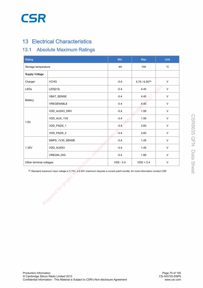
13 Electrical Characteristics13.1 Absolute Maximum Ratings
Rating Min Max Unit
Storage temperature -40 105 °C
Supply Voltage
Charger VCHG -0.4 5.75 / 6.50(a) V
LEDs LED[2:0] -0.4 4.40 V
BatteryVBAT_SENSE -0.4 4.40 V
VREGENABLE -0.4 4.40 V
1.8V
VDD_AUDIO_DRV -0.4 1.95 V
VDD_AUX_1V8 -0.4 1.95 V
VDD_PADS_1 -0.4 3.60 V
VDD_PADS_2 -0.4 3.60 V
1.35V
SMPS_1V35_SENSE -0.4 1.45 V
VDD_AUDIO -0.4 1.45 V
VREGIN_DIG -0.4 1.95 V
Other terminal voltages VSS - 0.4 VDD + 0.4 V
(a) Standard maximum input voltage is 5.75V, a 6.50V maximum requires a correct patch bundle, for more information contact CSR
Production Information© Cambridge Silicon Radio Limited 2013Confidential Information - This Material is Subject to CSR's Non-disclosure Agreement
Page 70 of 105CS-303725-DSP5
www.csr.com
CSR
8635 QFN D
ata Sheet
Prepa
red
for q
ingbo
keve
n.zh
ou -
exce
lpoint
.com
.cn -
Friday
, Sep
tem
ber 2
7, 2
013

13.2 Recommended Operating Conditions
Rating Min Typ Max Unit
Operating temperature range -40 20 85 °C
Supply Voltage
Charger VCHG 4.75 / 3.10(a) 5.00 5.75 / 6.50(b) V
LEDs LED[2:0] 1.10 3.70 4.30 V
BatteryVBAT_SENSE 0 3.70 4.25 V
VREGENABLE 0 3.70 4.25 V
1.8V
VDD_AUDIO_DRV 1.70 1.80 1.95 V
VDD_AUX_1V8 1.70 1.80 1.95 V
VDD_PADS_1 1.70 1.80 3.60 V
VDD_PADS_2 1.70 1.80 3.60 V
1.35V
SMPS_1V35_SENSE 1.30 1.35 1.45 V
VDD_AUDIO 1.30 1.35 1.45 V
VREGIN_DIG 1.30 1.35 or 1.80(c) 1.95 V
(a) Minimum input voltage of 4.75 V is required for full specification, regulator operates at reduced load current from 3.1 V(b) Standard maximum input voltage is 5.75 V, a 6.50 V maximum requires a correct patch bundle, for more information contact CSR(c) Typical value depends on output required by the low-voltage VDD_DIG linear regulator, see Section 13.3.2.2
Production Information© Cambridge Silicon Radio Limited 2013Confidential Information - This Material is Subject to CSR's Non-disclosure Agreement
Page 71 of 105CS-303725-DSP5
www.csr.com
CSR
8635 QFN D
ata Sheet
Prepa
red
for q
ingbo
keve
n.zh
ou -
exce
lpoint
.com
.cn -
Friday
, Sep
tem
ber 2
7, 2
013
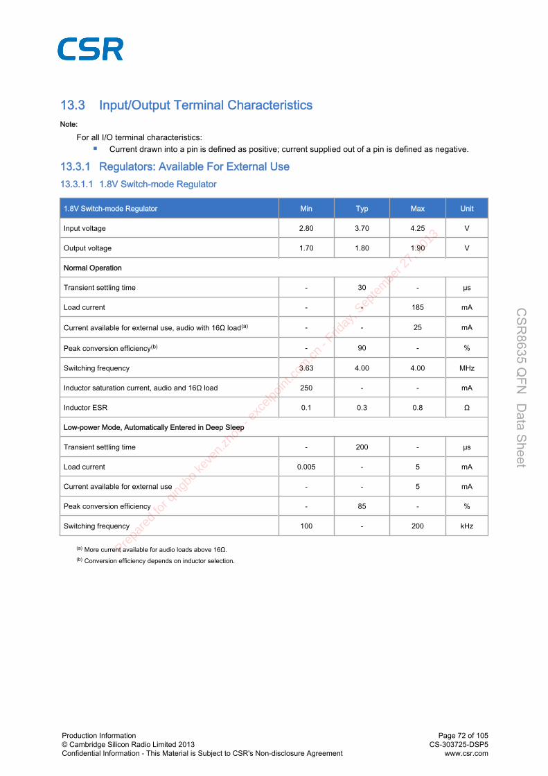
13.3 Input/Output Terminal CharacteristicsNote:
For all I/O terminal characteristics: Current drawn into a pin is defined as positive; current supplied out of a pin is defined as negative.
13.3.1 Regulators: Available For External Use13.3.1.1 1.8V Switch-mode Regulator
1.8V Switch-mode Regulator Min Typ Max Unit
Input voltage 2.80 3.70 4.25 V
Output voltage 1.70 1.80 1.90 V
Normal Operation
Transient settling time - 30 - μs
Load current - - 185 mA
Current available for external use, audio with 16Ω load(a) - - 25 mA
Peak conversion efficiency(b) - 90 - %
Switching frequency 3.63 4.00 4.00 MHz
Inductor saturation current, audio and 16Ω load 250 - - mA
Inductor ESR 0.1 0.3 0.8 Ω
Low-power Mode, Automatically Entered in Deep Sleep
Transient settling time - 200 - μs
Load current 0.005 - 5 mA
Current available for external use - - 5 mA
Peak conversion efficiency - 85 - %
Switching frequency 100 - 200 kHz
(a) More current available for audio loads above 16Ω.(b) Conversion efficiency depends on inductor selection.
Production Information© Cambridge Silicon Radio Limited 2013Confidential Information - This Material is Subject to CSR's Non-disclosure Agreement
Page 72 of 105CS-303725-DSP5
www.csr.com
CSR
8635 QFN D
ata Sheet
Prepa
red
for q
ingbo
keve
n.zh
ou -
exce
lpoint
.com
.cn -
Friday
, Sep
tem
ber 2
7, 2
013

13.3.1.2 Combined 1.8V and 1.35V Switch-mode Regulator
Combined 1.8V and 1.35V Switch-mode Regulator Min Typ Max Unit
Input voltage 2.80 3.60 4.25 V
Output voltage 1.70 1.80 1.90 V
Normal Operation
Transient settling time - 30 - μs
Load current - - 340 mA
Current available for external use, audio with 16Ω load(a) - - 25 mA
Peak conversion efficiency(b) - 90 - %
Switching frequency 3.63 4.00 4.00 MHz
Inductor saturation current, audio and 16Ω load 400 - - mA
Inductor ESR 0.1 0.3 0.8 Ω
Low-power Mode, Automatically Entered in Deep Sleep
Transient settling time - 200 - μs
Load current 0.005 - 5 mA
Current available for external use - - 5 mA
Peak conversion efficiency - 85 - %
Switching frequency 100 - 200 kHz
(a) More current available for audio loads above 16Ω.(b) Conversion efficiency depends on inductor selection.
Production Information© Cambridge Silicon Radio Limited 2013Confidential Information - This Material is Subject to CSR's Non-disclosure Agreement
Page 73 of 105CS-303725-DSP5
www.csr.com
CSR
8635 QFN D
ata Sheet
Prepa
red
for q
ingbo
keve
n.zh
ou -
exce
lpoint
.com
.cn -
Friday
, Sep
tem
ber 2
7, 2
013
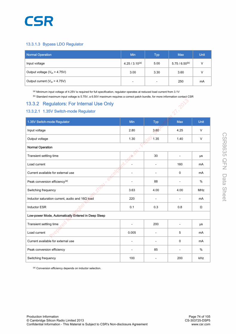
13.3.1.3 Bypass LDO Regulator
Normal Operation Min Typ Max Unit
Input voltage 4.25 / 3.10(a) 5.00 5.75 / 6.50(b) V
Output voltage (Vin > 4.75V) 3.00 3.30 3.60 V
Output current (Vin > 4.75V) - - 250 mA
(a) Minimum input voltage of 4.25V is required for full specification, regulator operates at reduced load current from 3.1V(b) Standard maximum input voltage is 5.75V, a 6.50V maximum requires a correct patch bundle, for more information contact CSR
13.3.2 Regulators: For Internal Use Only13.3.2.1 1.35V Switch-mode Regulator
1.35V Switch-mode Regulator Min Typ Max Unit
Input voltage 2.80 3.60 4.25 V
Output voltage 1.30 1.35 1.40 V
Normal Operation
Transient settling time - 30 - μs
Load current - - 160 mA
Current available for external use - - 0 mA
Peak conversion efficiency(a) - 88 - %
Switching frequency 3.63 4.00 4.00 MHz
Inductor saturation current, audio and 16Ω load 220 - - mA
Inductor ESR 0.1 0.3 0.8 Ω
Low-power Mode, Automatically Entered in Deep Sleep
Transient settling time - 200 - μs
Load current 0.005 - 5 mA
Current available for external use - - 0 mA
Peak conversion efficiency - 85 - %
Switching frequency 100 - 200 kHz
(a) Conversion efficiency depends on inductor selection.
Production Information© Cambridge Silicon Radio Limited 2013Confidential Information - This Material is Subject to CSR's Non-disclosure Agreement
Page 74 of 105CS-303725-DSP5
www.csr.com
CSR
8635 QFN D
ata Sheet
Prepa
red
for q
ingbo
keve
n.zh
ou -
exce
lpoint
.com
.cn -
Friday
, Sep
tem
ber 2
7, 2
013

13.3.2.2 Low-voltage VDD_DIG Linear Regulator
Normal Operation Min Typ Max Unit
Input voltage 1.30 1.35 or 1.80 1.95 V
Output voltage(a) 0.80 0.90 / 1.20 1.25 V
Internal load current - - 80 mA
(a) Output voltage level is software controlled
13.3.2.3 Low-voltage VDD_AUX Linear Regulator
Normal Operation Min Typ Max Unit
Input voltage 1.70 1.80 1.95 V
Output voltage 1.30 1.35 1.45 V
Internal load current - - 5 mA
13.3.2.4 Low-voltage VDD_ANA Linear Regulator
Normal Operation Min Typ Max Unit
Input voltage 1.70 1.80 1.95 V
Output voltage 1.30 1.35 1.45 V
Load current - - 60 mA
13.3.3 Regulator Enable
VREGENABLE, Switching Threshold Min Typ Max Unit
Rising threshold 1.0 - - V
13.3.4 Battery Charger
Battery Charger Min Typ Max Unit
Input voltage, VCHG 4.75 / 3.10(a) 5.00 5.75 / 6.50(b) V
(a) Reduced specification from 3.1V to 4.75V. Full specification >4.75V.(b) Standard maximum input voltage is 5.75V, a 6.50V maximum requires a correct patch bundle, for more information contact CSR.
Production Information© Cambridge Silicon Radio Limited 2013Confidential Information - This Material is Subject to CSR's Non-disclosure Agreement
Page 75 of 105CS-303725-DSP5
www.csr.com
CSR
8635 QFN D
ata Sheet
Prepa
red
for q
ingbo
keve
n.zh
ou -
exce
lpoint
.com
.cn -
Friday
, Sep
tem
ber 2
7, 2
013

Trickle Charge Mode Min Typ Max Unit
Charge current Itrickle, as percentage of fast charge current 8 10 12 %
Vfast rising threshold - 2.9 - V
Vfast rising threshold trim step size - 0.1 - V
Vfast falling threshold - 2.8 - V
Fast Charge Mode Min Typ Max Unit
Charge current during constant currentmode, Ifast
Maximum charge setting(VCHG-VBAT > 0.55V) 194 200 206 mA
Minimum charge setting(VCHG-VBAT > 0.55V) - 10 - mA
Reduced headroom charge current, asa percentage of Ifast
(VCHG-VBAT < 0.55V) 50 - 100 %
Charge current step size - 10 - mA
Vfloat threshold, calibrated 4.16 4.20 4.24 V
Charge termination current Iterm, as percentage of Ifast 7 10 20 %
Standby Mode Min Typ Max Unit
Voltage hysteresis on VBAT, Vhyst 100 - 150 mV
Error Charge Mode Min Typ Max Unit
Headroom(a) error falling threshold - 50 - mV
(a) Headroom = VCHG - VBAT
External Charge Mode(a) Min Typ Max Unit
Fast charge current, Ifast 200 - 500 mA
Control current into CHG_EXT 0 - 20 mA
Voltage on CHG_EXT 0 - 5.75 / 6.50(b) V
External pass device hfe - 50 - -
Sense voltage, between VBAT_SENSE and VBAT at maximumcurrent 195 200 205 mV
(a) In the external mode, the battery charger meets all the previous charger electrical characteristics and the additional or superseded electricalcharacteristics are listed in this table.
(b) Standard maximum input voltage is 5.75V, a 6.50V maximum requires a correct patch bundle, for more information contact CSR.
Production Information© Cambridge Silicon Radio Limited 2013Confidential Information - This Material is Subject to CSR's Non-disclosure Agreement
Page 76 of 105CS-303725-DSP5
www.csr.com
CSR
8635 QFN D
ata Sheet
Prepa
red
for q
ingbo
keve
n.zh
ou -
exce
lpoint
.com
.cn -
Friday
, Sep
tem
ber 2
7, 2
013
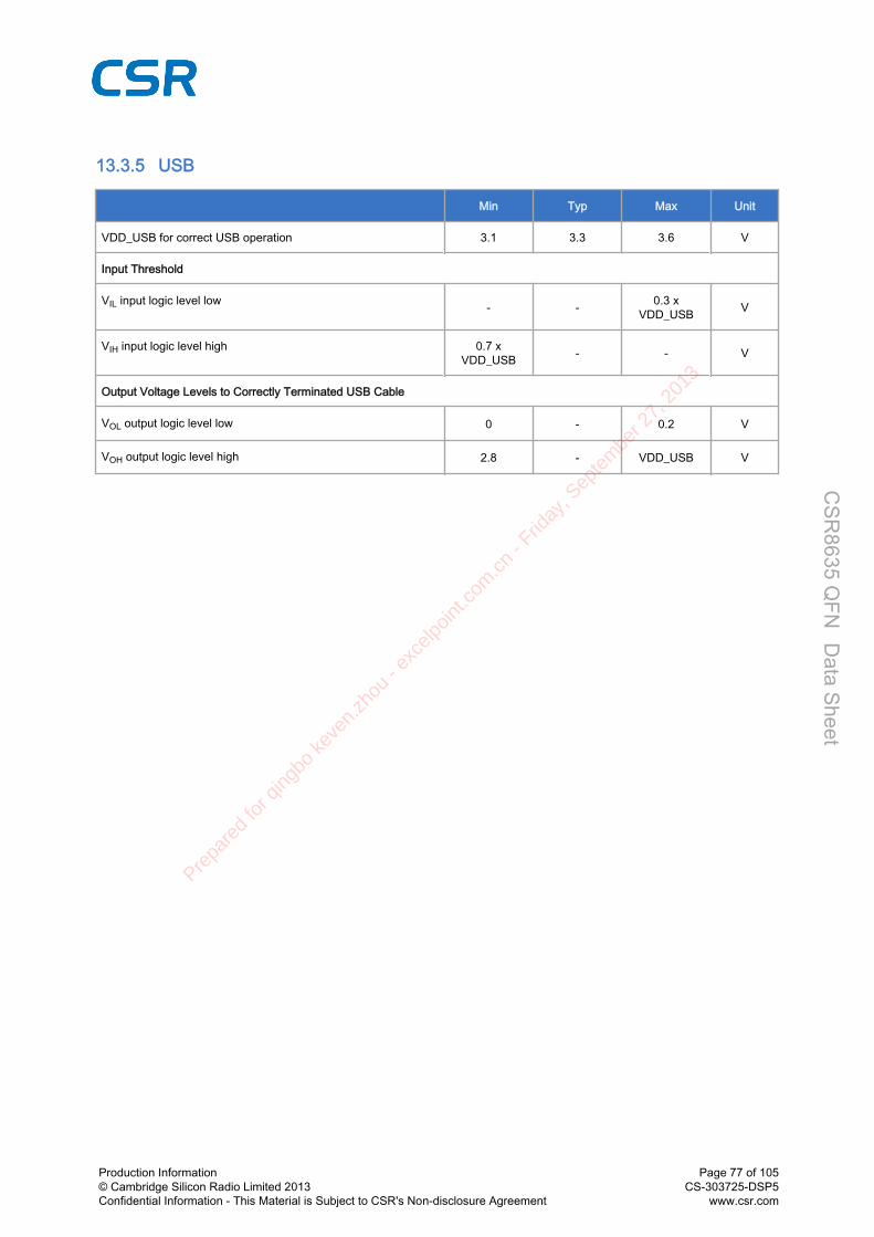
13.3.5 USB
Min Typ Max Unit
VDD_USB for correct USB operation 3.1 3.3 3.6 V
Input Threshold
VIL input logic level low - - 0.3 xVDD_USB V
VIH input logic level high 0.7 xVDD_USB - - V
Output Voltage Levels to Correctly Terminated USB Cable
VOL output logic level low 0 - 0.2 V
VOH output logic level high 2.8 - VDD_USB V
Production Information© Cambridge Silicon Radio Limited 2013Confidential Information - This Material is Subject to CSR's Non-disclosure Agreement
Page 77 of 105CS-303725-DSP5
www.csr.com
CSR
8635 QFN D
ata Sheet
Prepa
red
for q
ingbo
keve
n.zh
ou -
exce
lpoint
.com
.cn -
Friday
, Sep
tem
ber 2
7, 2
013

13.3.6 Stereo Codec: Analogue to Digital Converter
Analogue to Digital Converter
Parameter Conditions Min Typ Max Unit
Resolution - - - 16 Bits
Input Sample Rate,Fsample
- 8 - 48 kHz
Maximum ADC InputSignal Amplitude 0dB = 1600mVpk-pk 13 - 2260 mVpk-pk
SNR
fin = 1kHzB/W = 20Hz→Fsample/2(20kHz max)A-WeightedTHD+N < 0.1%1.6Vpk-pk input
Fsample
8kHz - 94.4 - dB
16kHz - 92.4 - dB
32kHz - 92.5 - dB
44.1kHz - 93.2 - dB
48kHz - 91.9 - dB
THD+N
fin = 1kHzB/W = 20Hz→Fsample/2(20kHz max)1.6Vpk-pk input
Fsample
8kHz - 0.004 - %
48kHz - 0.016 - %
Digital gain Digital gain resolution = 1/32 -24 - 21.5 dB
Analogue gain
Pre-amplifier setting = 0dB, 9dB, 21dB or30dBAnalogue setting = -3dB to 12dB in 3dBsteps
-3 - 42 dB
Stereo separation (crosstalk) - -89.9 - dB
Production Information© Cambridge Silicon Radio Limited 2013Confidential Information - This Material is Subject to CSR's Non-disclosure Agreement
Page 78 of 105CS-303725-DSP5
www.csr.com
CSR
8635 QFN D
ata Sheet
Prepa
red
for q
ingbo
keve
n.zh
ou -
exce
lpoint
.com
.cn -
Friday
, Sep
tem
ber 2
7, 2
013
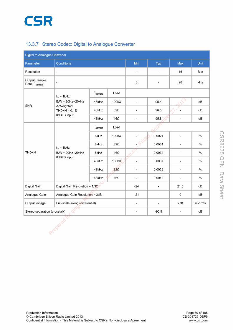
13.3.7 Stereo Codec: Digital to Analogue Converter
Digital to Analogue Converter
Parameter Conditions Min Typ Max Unit
Resolution - - - 16 Bits
Output SampleRate, Fsample
- 8 - 96 kHz
SNR
fin = 1kHzB/W = 20Hz→20kHzA-WeightedTHD+N < 0.1%0dBFS input
Fsample Load
48kHz 100kΩ - 95.4 - dB
48kHz 32Ω - 96.5 - dB
48kHz 16Ω - 95.8 - dB
THD+Nfin = 1kHzB/W = 20Hz→20kHz0dBFS input
Fsample Load
8kHz 100kΩ - 0.0021 - %
8kHz 32Ω - 0.0031 - %
8kHz 16Ω - 0.0034 - %
48kHz 100kΩ - 0.0037 - %
48kHz 32Ω - 0.0029 - %
48kHz 16Ω - 0.0042 - %
Digital Gain Digital Gain Resolution = 1/32 -24 - 21.5 dB
Analogue Gain Analogue Gain Resolution = 3dB -21 - 0 dB
Output voltage Full-scale swing (differential) - - 778 mV rms
Stereo separation (crosstalk) - -90.5 - dB
Production Information© Cambridge Silicon Radio Limited 2013Confidential Information - This Material is Subject to CSR's Non-disclosure Agreement
Page 79 of 105CS-303725-DSP5
www.csr.com
CSR
8635 QFN D
ata Sheet
Prepa
red
for q
ingbo
keve
n.zh
ou -
exce
lpoint
.com
.cn -
Friday
, Sep
tem
ber 2
7, 2
013

13.3.8 Digital
Digital Terminals Min Typ Max Unit
Input Voltage
VIL input logic level low -0.4 - 0.4 V
VIH input logic level high 0.7 x VDD - VDD + 0.4 V
Tr/Tf - - 25 ns
Output Voltage
VOL output logic level low, lOL = 4.0mA - - 0.4 V
VOH output logic level high, lOH = -4.0mA 0.75 X VDD - - V
Tr/Tf - - 5 ns
Input and Tristate Currents
Strong pull-up -150 -40 -10 μA
Strong pull-down 10 40 150 μA
Weak pull-up -5 -1.0 -0.33 μA
Weak pull-down 0.33 1.0 5.0 μA
CI Input Capacitance 1.0 - 5.0 pF
13.3.9 LED Driver Pads
LED Driver Pads Min Typ Max Unit
Current, IPAD
High impedance state - - 5 µA
Current sink state - - 10 mA
LED pad voltage, VPAD IPAD = 10mA - - 0.55 V
LED pad resistance VPAD < 0.5V - - 40 Ω
VOL output logic level low(a) - 0 - V
VOH output logic level high(a) - 0.8 - V
VIL input logic level low - 0 - V
VIH input logic level high - 0.8 - V
(a) LED output port is open-drain and requires a pull-up
Production Information© Cambridge Silicon Radio Limited 2013Confidential Information - This Material is Subject to CSR's Non-disclosure Agreement
Page 80 of 105CS-303725-DSP5
www.csr.com
CSR
8635 QFN D
ata Sheet
Prepa
red
for q
ingbo
keve
n.zh
ou -
exce
lpoint
.com
.cn -
Friday
, Sep
tem
ber 2
7, 2
013

13.3.10 Auxiliary ADC
Auxiliary ADC Min Typ Max Unit
Resolution - - 10 Bits
Input voltage range(a) 0 - VDD_AUX V
Accuracy(Guaranteed monotonic)
INL -1 - 1 LSB
DNL 0 - 1 LSB
Offset -1 - 1 LSB
Gain error -0.8 - 0.8 %
Input bandwidth - 100 - kHz
Conversion time 1.38 1.69 2.75 µs
Sample rate(b) - - 700 Samples/s
(a) LSB size = VDD_AUX/1023(b) The auxiliary ADC is accessed through a VM function. The sample rate given is achieved as part of this function.
13.3.11 Auxiliary DAC
Auxiliary DAC Min Typ Max Unit
Resolution - - 10 Bits
Supply voltage, VDD_AUX 1.30 1.35 1.40 V
Output voltage range 0 - VDD_AUX V
Full-scale output voltage 1.30 1.35 1.40 V
LSB size 0 1.32 2.64 mV
Offset -1.32 0 1.32 mV
Integral non-linearity -1 0 1 LSB
Settling time(a) - - 250 ns
(a) The settling time does not include any capacitive load
Important Note:
Access to the auxiliary DAC is firmware-dependent, for more information about its availability contact CSR.
Production Information© Cambridge Silicon Radio Limited 2013Confidential Information - This Material is Subject to CSR's Non-disclosure Agreement
Page 81 of 105CS-303725-DSP5
www.csr.com
CSR
8635 QFN D
ata Sheet
Prepa
red
for q
ingbo
keve
n.zh
ou -
exce
lpoint
.com
.cn -
Friday
, Sep
tem
ber 2
7, 2
013

13.4 ESD ProtectionApply ESD static handling precautions during manufacturing.
Table 13.1 shows the ESD handling maximum ratings.
Condition Class Max Rating
Human Body Model Contact Discharge perANSI/ESDA/JEDEC JS‑001
2 2kV (all pins except CHG_EXT; CHG_EXT israted at 1kV)
Charged Device Model Contact Discharge perJEDEC/EIA JESD22‑C101
III 500V (all pins)
Table 13.1: ESD Handling Ratings
13.4.1 USB Electrostatic Discharge ImmunityCSR8635 QFN has integrated ESD protection on the USB_DP and USB_DN pins as detailed in IEC 61000‑4‑2.
CSR has tested CSR8635 QFN assembled in development kits to assess the Electrostatic Discharge Immunity. Thetests were based on IEC 61000‑4‑2 requirements. Tests were performed up to level 4 (8kV contact discharge / 15kVair discharge).
CSR can demonstrate normal performance up to level 2 (4kV contact discharge / 4kV air discharge) as per IEC 6100-4-2classification 1. Above level 2, temporary degradation is seen (classification 2).
CSR8635 QFN contains a reset protection circuit and software, which will attempt to re-make any connections lost ina ESD event. If the device at the far end permits this, self-recovery of the Bluetooth link is possible if CSR8635 QFNresets on an ESD strike. This classes CSR8635 QFN as IEC 61000‑4‑2 classification 2 to level 4 (8kV contactdischarge / 15kV air discharge). If self-recovery is not implemented, CSR8635 QFN is IEC 61000‑4‑2 classification 3to level 4.
Note:
Any test detailed in the IEC-61000-4-2 level 4 test specification does not damage CSR8635 QFN.
The CSR8635 QFN USB VBUS pin is protected to level 4 using an external 2.2µF decoupling capacitor on VCHG.
Important Note:
CSR recommends correct PCB routing and to route the VBUS track through a decoupling capacitor pad.
When the USB connector is a long way from CSR8635 QFN, place an extra 1µF or 2.2µF capacitor near the USBconnector.
No components (including 22Ω series resistors) are required between CSR8635 QFN and the USB_DP andUSB_DN lines.
To recover from an unintended reset, e.g. a large ESD strike, the watchdog and reset protection feature can restartCSR8635 QFN and signal the unintended reset to the VM.
Table 13.2 summarises the level of protection.
Production Information© Cambridge Silicon Radio Limited 2013Confidential Information - This Material is Subject to CSR's Non-disclosure Agreement
Page 82 of 105CS-303725-DSP5
www.csr.com
CSR
8635 QFN D
ata Sheet
Prepa
red
for q
ingbo
keve
n.zh
ou -
exce
lpoint
.com
.cn -
Friday
, Sep
tem
ber 2
7, 2
013

IEC 61000‑4‑2Level
ESD Test Voltage(Positive and Negative)
IEC 61000‑4‑2Classification
Comments
1 2kV contact / 2kV air Class 1 Normal performance within specificationlimits
2 4kV contact / 4kV air Class 1 Normal performance within specificationlimits
3 6kV contact / 8kV air Class 2 or class 3 Temporary degradation or operatorintervention required
4 8kV contact / 15kV air Class 2 or class 3 Temporary degradation or operatorintervention required
Table 13.2: USB Electrostatic Discharge Protection Level
For more information contact CSR.
Production Information© Cambridge Silicon Radio Limited 2013Confidential Information - This Material is Subject to CSR's Non-disclosure Agreement
Page 83 of 105CS-303725-DSP5
www.csr.com
CSR
8635 QFN D
ata Sheet
Prepa
red
for q
ingbo
keve
n.zh
ou -
exce
lpoint
.com
.cn -
Friday
, Sep
tem
ber 2
7, 2
013

14 Power Consumption
DUT Role Connection Packet Type Packet Size AverageCurrent Unit
Slave SCO HV3 30 11.0 mA
Slave eSCO EV3 30 11.8 mA
Slave eSCO 3EV3 60 9.2 mA
Slave SCO1-mic CVC: 8kHz sampling Narrowband
HV3 30 12.6 mA
Slave eSCO1-mic CVC: 8kHz sampling Narrowband
2EV3 60 10.8 mA
Slave eSCO1-mic CVC: 16kHz sampling Wideband
2EV3 60 11.4 mA
Slave eSCO1-mic CVC: 16kHz sampling FESI
2EV3 60 10.9 mA
Slave SCO1-mic CVC hands-free: 8kHz sampling Narrowband
HV3 30 12.2 mA
Slave eSCO1-mic CVC hands-free: 8kHz sampling Narrowband
2EV3 60 10.4 mA
Slave eSCO1-mic CVC hands-free: 16kHz sampling Wideband
2EV3 60 11.2 mA
Slave eSCO1-mic CVC hands-free: 16kHz sampling FESI
2EV3 60 10.7 mA
Slave
A2DP Stereo streaming SBC high quality: Bit-Pool = 50, 16 blocks and 8 sub-
bands 48kHz sampling No sniff White noise
- - 13.3 mA
Production Information© Cambridge Silicon Radio Limited 2013Confidential Information - This Material is Subject to CSR's Non-disclosure Agreement
Page 84 of 105CS-303725-DSP5
www.csr.com
CSR
8635 QFN D
ata Sheet
Prepa
red
for q
ingbo
keve
n.zh
ou -
exce
lpoint
.com
.cn -
Friday
, Sep
tem
ber 2
7, 2
013

DUT Role Connection Packet Type Packet Size AverageCurrent Unit
Slave
A2DP Stereo streaming SBC low quality: Bit-Pool = 20, 16 blocks and 8 sub-
bands 48kHz sampling No sniff White noise
- - 11.8 mA
Slave ACL Sniff = 500ms - - 213 µA
Slave ACL Sniff = 1280ms - - 142 µA
Master SCO HV3 30 10.8 mA
Master eSCO EV3 30 11.2 mA
Master eSCO 3EV3 60 8.8 mA
Master SCO1-mic CVC: 8kHz sampling Narrowband
HV3 30 12.5 mA
Master eSCO1-mic CVC: 8kHz sampling Narrowband
2EV3 60 10.5 mA
Master eSCO1-mic CVC: 16kHz sampling Wideband
2EV3 60 11.0 mA
Master eSCO1-mic CVC: 16kHz sampling FESI
2EV3 60 10.6 mA
Master SCO1-mic CVC hands-free: 8kHz sampling Narrowband
HV3 30 12.1 mA
Master eSCO1-mic CVC hands-free: 8kHz sampling Narrowband
2EV3 60 10.1 mA
Production Information© Cambridge Silicon Radio Limited 2013Confidential Information - This Material is Subject to CSR's Non-disclosure Agreement
Page 85 of 105CS-303725-DSP5
www.csr.com
CSR
8635 QFN D
ata Sheet
Prepa
red
for q
ingbo
keve
n.zh
ou -
exce
lpoint
.com
.cn -
Friday
, Sep
tem
ber 2
7, 2
013

DUT Role Connection Packet Type Packet Size AverageCurrent Unit
Master eSCO1-mic CVC hands-free: 16kHz sampling Wideband
2EV3 60 10.8 mA
Master eSCO1-mic CVC hands-free: 16kHz sampling FESI
2EV3 60 10.2 mA
Master
A2DP Stereo streaming SBC high quality: Bit-Pool = 50, 16 blocks and 8 sub-
bands 48kHz sampling No sniff White noise
- - 13.2 mA
Master
A2DP Stereo streaming SBC low quality: Bit-Pool = 20, 16 blocks and 8 sub-
bands 48kHz sampling No sniff White noise
- - 10.9 mA
Master ACL Sniff = 500ms - - 197 µA
Master ACL Sniff = 1280ms - - 142 µA
Note:
Current consumption values are taken with: VBAT pin = 3.7V RF TX power set to 0dBm No RF retransmissions in case of eSCO Microphones and speakers disconnected Audio gateway transmits silence when SCO/eSCO channel is open LEDs disconnected AFH classification master disabled
Production Information© Cambridge Silicon Radio Limited 2013Confidential Information - This Material is Subject to CSR's Non-disclosure Agreement
Page 86 of 105CS-303725-DSP5
www.csr.com
CSR
8635 QFN D
ata Sheet
Prepa
red
for q
ingbo
keve
n.zh
ou -
exce
lpoint
.com
.cn -
Friday
, Sep
tem
ber 2
7, 2
013

15 CSR Green Semiconductor Products and RoHS ComplianceCSR confirms that CSR Green semiconductor products comply with the following regulatory requirements:
Restriction on Hazardous Substances directive guidelines in the EU RoHS Directive 2011/65/EU1. EU REACH, Regulation (EC) No 1907/20061:
List of substances subject to authorisation (Annex XIV) Restrictions on the manufacture, placing on the market and use of certain dangerous substances,
preparations and articles (Annex XVII). This Annex now includes requirements that were contained withinEU Directive, 76/769/EEC. There are many substance restrictions within this Annex, including, but notlimited to, the control of use of Perfluorooctane sulfonates (PFOS).
When requested by customers, notification of substances identified on the Candidate List as Substancesof Very High Concern (SVHC)1.
POP regulation (EC) No 850/20041
EU Packaging and Packaging Waste, Directive 94/62/EC1
Montreal Protocol on substances that deplete the ozone layer. Conflict minerals, Section 1502, Dodd-Frank Wall Street Reform and Consumer Protection act, which affects
columbite-tantalite (coltan / tantalum), cassiterite (tin), gold, wolframite (tungsten) or their derivatives. CSR isa fabless semiconductor company: all manufacturing is performed by key suppliers. CSR have mandated thatthe suppliers shall not use materials that are sourced from "conflict zone mines" but understand that thisrequires accurate data from the EICC programme. CSR shall provide a complete EICC / GeSI template uponrequest.
CSR has defined the "CSR Green" standard based on current regulatory and customer requirements including freefrom bromine, chlorine and antimony trioxide.
Products and shipment packaging are marked and labelled with applicable environmental marking symbols inaccordance with relevant regulatory requirements.
This identifies the main environmental compliance regulatory restrictions CSR specify. For more information on the full"CSR Green" standard, contact [email protected].
1 Including applicable amendments to EU law which are published in the EU Official Journal, or SVHCCandidate List updates published by the European Chemicals Agency (ECHA).
Production Information© Cambridge Silicon Radio Limited 2013Confidential Information - This Material is Subject to CSR's Non-disclosure Agreement
Page 87 of 105CS-303725-DSP5
www.csr.com
CSR
8635 QFN D
ata Sheet
Prepa
red
for q
ingbo
keve
n.zh
ou -
exce
lpoint
.com
.cn -
Friday
, Sep
tem
ber 2
7, 2
013

16 SoftwareCSR8635 QFN:
Includes integrated Bluetooth v4.0 specification qualified HCI stack firmware Includes integrated CSR8635 Stereo ROM Solution, with 6th generation 1-mic CVC audio enhancements and
a configurable EQ Can be shipped with CSR’s CSR8635 stereo ROM solution development kit for CSR8635 QFN, order code
DK‑8635‑10163‑1A
The CSR8635 QFN software architecture enables Bluetooth processing and the application program to run on theinternal RISC MCU, and the audio enhancements on the Kalimba DSP.
16.1 CSR8635 Stereo ROM SolutionThe CSR8635 stereo ROM solution software supports:
6th generation 1-mic CVC audio enhancements WNR PLC / BEC mSBC wideband speech codec A2DP v1.2 HFP v1.6 and HSP v1.2 SCMS-T Bluetooth v4.0 specification is supported in the ROM software Secure simple pairing Proximity pairing (device-initiated pairing) for greatly simplifying the out-of-box pairing process, for more
information see Section 16.1.8 For connection to more than 1 mobile phone, advanced Multipoint is supported. This enables a user to take
calls from a work and personal phone or a work phone and a VoIP dongle for Skype users. This has minimalimpact on power consumption and is easy to configure.
Most of the CSR8635 stereo ROM solution ROM software features are configured on the CSR8635 QFN usingthe Headset Configuration Tool. The tool reads and writes device configurations directly to the EEPROM,serial flash or alternatively to a PSR file. Configurable device features include: Bluetooth v4.0 specification features Reconnection policies, e.g. reconnect on power-on Audio features, including default volumes Button events: configuring button presses and durations for certain events, e.g. double press on PIO[1]
for last number redial LED indications for states, e.g. device connected, and events, e.g. power on Indication tones for events and ringtones HFP v1.6 supported features Battery divider ratios and thresholds, e.g. thresholds for battery low indication, full battery etc. Advanced Multipoint settings
Configurable 5-band EQ for music playback (rock, pop, classical, jazz, dance etc) AAC, SBC, MP3 and Faststream decoder Stereo widening (S3D) Volume Boost USB audio mode for streaming high-quality music from a PC whilst charging, enables the device to:
Playback high-quality stereo music, e.g. iTunes Use bidirectional audio in conversation mode, e.g. for Skype
Wired audio mode for pendant-style devices supports music playback using a line-in jack. Enables nonBluetooth operation in low battery modes or when using the device in an airplane-mode.
Support for smartphone applications (apps) The CSR8635 stereo ROM solution has undergone extensive interoperability testing to ensure it works with
the majority of phones on the market
Production Information© Cambridge Silicon Radio Limited 2013Confidential Information - This Material is Subject to CSR's Non-disclosure Agreement
Page 88 of 105CS-303725-DSP5
www.csr.com
CSR
8635 QFN D
ata Sheet
Prepa
red
for q
ingbo
keve
n.zh
ou -
exce
lpoint
.com
.cn -
Friday
, Sep
tem
ber 2
7, 2
013

16.1.1 Advanced Multipoint SupportAdvanced Multipoint enables the connection of 2 devices to a CSR8635 QFN device at the same time, examplesinclude:
2 phones connected to a CSR8635 QFN device Phone and a VoIP dongle connected to a CSR8635 QFN device Phone and tablet
The CSR8635 stereo ROM solution: Supports up to 2 simultaneous connections (either HFP or HSP) Enables multiple-call handling from both devices at the same time Treats all device buttons:
During a call from one device, as if there is 1 device connected During multiple calls (1 on each device), as if there is a single AG with multiple calls in progress (three-
way calling) During multiple calls (more than 1 on each device), as if there are multiple calls on a single device enabling
the user to switch between the active and held calls
16.1.2 A2DP Multipoint SupportA2DP Multipoint support enables the connection of 2 A2DP source devices to CSR8635 QFN at the same time,examples include:
2 A2DP-capable phones connected to a CSR8635 QFN device A2DP-capable phone and an A2DP-only source device, e.g. a PC or an iPod touch
The CSR8635 stereo ROM solution enables: Music streaming from either of the connected A2DP source devices where the music player is controlled on
the source device Advanced HFP Multipoint functions to interrupt music streaming for calls, and resume music streaming on the
completion of the calls AVRCP v1.4 connections to both connected devices, enabling the device to remotely control the primary
device, i.e. the device currently streaming audio
16.1.3 Wired Audio ModeCSR8635 QFN supports a wired audio mode for playing music over a wired connection.
If CSR8635 QFN is powered, the audio path is routed through CSR8635 QFN, including via the DSP, this enables theCSR8635 QFN to:
Mix audio sources, e.g. tones and programmable audio prompts Control the volume of the audio, i.e. volume up and volume down Utilise the 5 band EQ
In wired audio mode, if required, the CSR8635 QFN is still available for Bluetooth audio. This enables seamlesstransition from wired audio mode to Bluetooth audio mode and back again. This transition is configurable to occurautomatically as the battery voltage of the device reduces to a point at which Bluetooth audio is no longer possible.
The carrier board features a stereo line-in with detect.
16.1.4 USB Modes Including USB Audio ModeCSR8635 QFN supports a variety of USB modes which enables the USB interface to extend the functionality of aCSR8635 QFN based stereo device.
CSR8635 QFN supports: USB charger enumeration USB soundcard enumeration (USB audio mode) USB mass storage enumeration
USB audio mode enables the device to enumerate as a soundcard while charging from a USB master device, e.g. aPC. In this mode, the device enumerates as either a stereo music soundcard (for high quality music playback) or abidirectional voice quality soundcard. This enables the device for either listening to music streaming from the USB hostdevice or for voice applications, e.g. Skype.
Production Information© Cambridge Silicon Radio Limited 2013Confidential Information - This Material is Subject to CSR's Non-disclosure Agreement
Page 89 of 105CS-303725-DSP5
www.csr.com
CSR
8635 QFN D
ata Sheet
Prepa
red
for q
ingbo
keve
n.zh
ou -
exce
lpoint
.com
.cn -
Friday
, Sep
tem
ber 2
7, 2
013

The USB audio mode operates at the same time as the wired audio mode and the USB audio interrupts the wired audiomode if USB audio is attached. This enables a device to have both wired audio and USB modes connected at the sametime.
In USB audio mode, if required, the device is still available for Bluetooth audio.
16.1.5 Smartphone Applications (Apps)CSR8635 QFN includes CSR’s proprietary mechanism for communicating with smartphone apps, it enables full UIcontrol of the device from within the application running on a smartphone, e.g. Google Android OS-based handset. Formore information on this feature contact CSR.
16.1.6 Programmable Audio PromptsCSR8635 QFN enables a user to configure and load pre-programmed audio prompts from:
An external EEPROM, in this implementation the prompts are stored in the same EEPROM as the PS Keys,see Figure 16.2. A larger EEPROM is necessary for programmable audio prompts. This implementationsupports EEPROMs up to 512Kb. An EEPROM of 512Kb enables approximately 15 seconds of audio storage.
An external SPI flash, in this implementation the prompts are stored in the same SPI flash as the PS Keys,see Figure 16.1.
The programmable audio prompts provide a mechanism for higher-quality audio indications to replace standard toneindications. A programmable audio prompt is assigned to any user event in place of a standard tone.
Programmable audio prompts contain either voice prompts to indicate that events have occurred or provide user-definedhigher quality ring tones/indications, e.g. custom power on/off tones.
The Headset Configuration Tool can generate the content for the programmable audio prompts from standard WAVaudio files. The tool also enables the user to configure which prompts are assigned to which user events.
Section 6.5 describes the SPI flash interface and Section 7.4 describes the I²C interface to an external EEPROM.
G-T
W-0
0129
61.1
.1
CSR8635
SPI Flash
SPI
PS Keys
Programmable Audio Prompts
Patches
Configuration
Figure 16.1: Programmable Audio Prompts in External SPI Flash
Production Information© Cambridge Silicon Radio Limited 2013Confidential Information - This Material is Subject to CSR's Non-disclosure Agreement
Page 90 of 105CS-303725-DSP5
www.csr.com
CSR
8635 QFN D
ata Sheet
Prepa
red
for q
ingbo
keve
n.zh
ou -
exce
lpoint
.com
.cn -
Friday
, Sep
tem
ber 2
7, 2
013

G-T
W-0
0129
62.1
.1
CSR8635
EEPROM
I2C
PS Keys
Programmable Audio Prompts
Patches
Configuration
Figure 16.2: Programmable Audio Prompts in External I²C EEPROM
Note:
When using the SPI flash interface for programmable audio prompts, an EEPROM device is not required in theCSR8635 stereo ROM solution.
16.1.7 CSR’s Intelligent Power ManagementIPM extends the available talk time of a CSR8635 QFN-based device, by automatically reducing the audio processingperformed by CVC at a series of low battery capacity thresholds.
Configurable IPM features include: IPM enable/disable The battery capacity that engages IPM A user-action to enable or disable the IPM
If engaged, CVC processing reduces automatically on reaching the preset battery capacity. Once the audio isterminated, the DSP shuts down to achieve maximum power savings before the next call.
IPM resets when recharging the device. The talk time extension depends on: The battery size The battery condition The threshold capacity configured for the IPM to engage
16.1.8 Proximity PairingProximity pairing is device-initiated pairing and it simplifies the out-of-box pairing process. Proximity pairing enablesthe device to find the closest discoverable phone. The device then initiates the pairing activity and the user simply hasto accept the incoming pairing invitation on the phone.
This means that the phone-user does not have to hunt through phone menus to pair with the new device.
Depending on the phone UI: For a Bluetooth v2.0 phone the device pairing is with a PIN code For a Bluetooth v2.1 (or above) phone the device pairing is without a PIN code
Proximity pairing is based on finding and pairing with the closest phone. To do this, the device finds the loudest phoneby carrying out RSSI power threshold measurements. The loudest phone is the one with the largest RSSI powerthreshold measurement, and it is defined as the closest device. The device then attempts to pair with and connect tothis device.
Proximity pairing is configurable using the Headset Configuration Tool available from www.csrsupport.com.
16.1.9 Proximity ConnectionProximity connection is an extension to proximity pairing, see Section 16.1.8. It enables the device‑user to takeadvantage of the proximity of devices each time the device powers up and not just during a first time pairing event.
Proximity connection enables a user with multiple handsets to easily connect to the closest discoverable phone bycomparing the proximity of devices to the device at power-on to the list of previously paired devices.
Production Information© Cambridge Silicon Radio Limited 2013Confidential Information - This Material is Subject to CSR's Non-disclosure Agreement
Page 91 of 105CS-303725-DSP5
www.csr.com
CSR
8635 QFN D
ata Sheet
Prepa
red
for q
ingbo
keve
n.zh
ou -
exce
lpoint
.com
.cn -
Friday
, Sep
tem
ber 2
7, 2
013

Proximity connection speeds up the device connection process. It requires the device to initiate a SLC connection tothe nearest device first and combines this with the device's storage of the last 8 paired/connected devices. Usingproximity connection means functions operate equally well for the most or least recently paired or connected device.
16.2 6th Generation 1-mic CVC ENR Technology for Hands-free and AudioEnhancements
1-mic CVC full-duplex voice processing software is a fully integrated and highly optimised set of DSP algorithmsdeveloped to ensure easy design and build of hands-free products.
CVC enables greater acoustic design flexibility for a wide variety of environments and configurations as a result ofsophisticated noise and echo suppression technology. CVC reduces the affects of noise on both sides of theconversation and smartly adjusts the receive volume levels and dynamically frequency shapes the voice to achieveoptimal intelligibility and comfort for the hands-free user.
The 6th generation CVC features include: Full-duplex AEC Bit error and packet loss concealment Transmit and receive noise suppression including WNR Transmit and receive Parametric Equalisation Transmit and receive AGC Noise dependent volume control Receive frequency enhanced speech intelligibility using adaptive equaliser Narrowband, wideband and frequency expansion operations
1-mic CVC includes a tuning tool enabling the developer to easily adapt CVC with different audio configurations andtuning parameters. The tool provides real-time system statistics with immediate feedback enabling designers to quicklyinvestigate the effect of changes.
Figure 16.3 shows the functional block diagram of CSR’s proprietary 1-mic CVC DSP solution for a hands-free product.
G-T
W-0
0101
88.1
.1
Packet Loss Concealment
Noise Suppression
Adaptive Equaliser
Receive EqualiserReceive AGCClipper
Send AGCSend EqualiserComfort NoiseNoise Suppression
NDVC
Auxiliary Stream Mix
Acoustic Echo Canceller
Mic Gain
Speaker Gain
Bluetooth R
adio
Nonlinear Processing
Howling Control
Send In
Send Out
Receive Out
Receive In
Figure 16.3: 1-mic CVC Block Diagram
Section 16.2.1 to Section 16.2.13 describe the audio processing functions provided within CVC.
16.2.1 Acoustic Echo CancellationThe AEC includes:
A referenced sub-band adaptive linear filter that models the acoustic path from the receive reference point tothe microphone input
A non-linear processing function that applies narrowband and wideband attenuation adaptively as a result ofresidual echo present after the linear filter.
Production Information© Cambridge Silicon Radio Limited 2013Confidential Information - This Material is Subject to CSR's Non-disclosure Agreement
Page 92 of 105CS-303725-DSP5
www.csr.com
CSR
8635 QFN D
ata Sheet
Prepa
red
for q
ingbo
keve
n.zh
ou -
exce
lpoint
.com
.cn -
Friday
, Sep
tem
ber 2
7, 2
013

16.2.2 Noise Suppression with Wind Noise ReductionThe signal-channel noise suppression block is implemented in both signal paths. They are completely independent andindividually tuned. Noise suppression is a sub-band stationary / quasi-stationary noise suppression algorithm that usesthe temporal characteristics of speech and noise to remove the noise from the composite signal while maximisingspeech quality. The current implementation can improve the SNR by up to 20dB.
In the transmit path, noise suppression aggressiveness is typically 95% improving SNR by 15 to 19dB to compensatefor the upstream processing and to maintain superior voice quality, while the Rx is typically tuned down to 80% improvingSNR by 8 to 12dB because of the cellular network processing. The user can parametrically adjust these default settings.
The noise suppression block contains a new WNR feature (send path only). The WNR removes unwanted noise duringa hands-free conversation, cleaning the audio for the far-end listener. It detects and tackle winds of various intensitiesand durations. Once the wind is detected, a good balance between voice quality and WNR is achieved.
16.2.3 Non-linear Processing (NLP)The non-linear processing module detects the presence of echo after the primary sub-band linear filter and adaptivelyapplies attenuation at frequencies where echo is identified. It is used to minimise echo due to non-linearity caused bythe system, i.e. the loudspeaker and microphone, amplifiers, electronics etc. CSR recommends minimal use of non-linear processing due to the inherent distortion that it introduces.
16.2.4 Howling Control (HC)The Howling Control is a programmable coupling threshold that when triggered applies attenuation to the send path.This control enables CVC to operate in car-to-car calls without experiencing echo events during very high volumesituations.
16.2.5 Comfort Noise GeneratorThe CNG:
Creates a spectrally and temporally consistent noise floor for the far-end listener. Adaptively inserts noise modelled from the noise present at the microphone into gaps introduced when the
non-linear processing of the AEC applies attenuation. The noise level applied is user-controllable.
16.2.6 EqualisationThe equalisation filters:
Are independent in the send and receive signal channels Are independently enabled Are configurable to achieve the required frequency response Each channel comprises of 5 stages of cascaded 2nd order IIR filters Compensate for the frequency response of transducers in the system, i.e. the microphone and loud speaker
16.2.7 Automatic Gain ControlThe AGC block attempts to:
Normalise the amplitude of the incoming audio signal to a desired range to increase perceived loudness Reduce distortion due to clipping Reduce amplitude variance observed from different users, phones and networks
Maintaining a consistent long-term loudness for the speech ensures it is more easily heard by the listener and it alsoprovides the subsequent processing block a larger amplitude signal to process. The behaviour of the AGC differs froma dynamic range audio compressor. The convergence time for the AGC is much slower to reduce the non-lineardistortion.
16.2.8 Packet Loss ConcealmentBit errors and packet loss can occur in the Bluetooth transmission due to a variety of reasons, e.g. Wi-Fi interferenceor RF signal degradation due to distance or physical objects. As a result of these errors, the user hears glitches referredto as pops and clicks in the audio stream. The PLC block improves the receive path audio quality in the presence ofbit and packet errors within the Bluetooth link by using a variety of techniques such as pitch-based waveformsubstitution.
Production Information© Cambridge Silicon Radio Limited 2013Confidential Information - This Material is Subject to CSR's Non-disclosure Agreement
Page 93 of 105CS-303725-DSP5
www.csr.com
CSR
8635 QFN D
ata Sheet
Prepa
red
for q
ingbo
keve
n.zh
ou -
exce
lpoint
.com
.cn -
Friday
, Sep
tem
ber 2
7, 2
013

The PLC tries to re-synthesise the lost packet from the history buffer with the same pitch period. The PLC uses a highlyefficient 3-phase pitch estimator and performs cross-fading at the concatenation boundaries, i.e. the PLC attempts toclean up the audio signal by removing the pops and clicks and smoothing out gaps. This improves the audio quality forthe user and the improved signal enables proceding processing blocks to perform better.
The PLC significantly improves dealing with bit errors, using the BFI output from the firmware. The DSP calculates anaverage BER and selectively applies the PLC to the incoming data. This optimises audio quality for a variety of bit errorsand packet loss conditions. The PLC is enabled in all modes.
Note:
The PLC is enabled in all modes, HFK (full processing), pass-through and loopback by default.
16.2.9 Adaptive Equalisation (AEQ)The adaptive equalisation block improves the intelligibility of the receive path voice signal in the presence of near endnoise by altering the spectral shape of the receive path signal while maintaining the overall power level. It has beenempirically observed that consonants, which are dominantly high frequency based and much lower in amplitude thanvowels, significantly contribute to the intelligibility of the voice signal. In the presence of noise, the lower amplitudeconsonants become masked by this noise. Therefore, by increasing the frequency components that contribute to theconsonants while in the presence of noise, the intelligibility can be improved. In order to maintain a consistent amplitudelevel, the adaptive equalization block will adaptively increase the high frequencies relative to the middle frequenciesand also reduce the low frequencies accordingly. The adaptive equalizer also has the capability to compensate forvariations in voice transmission channels, which include farend devices and telecommunication channels.
The Frequency Emphasis feature can be used with any standard narrow band call, when the DAC is operating at asample rate of 8kHz. To complement the AEQ, High Frequency Emphasis can be added to improve the intelligibility ofthe far end caller. The emphasis feature repairs frequencies (3469Hz to 4000Hz) that were lost due to the filters of thecellular network and Bluetooth link. Information contained in the original speech from 281Hz to 3469Hz is used toreconstruct the lost high frequency content.
The Frequency Expansion feature can be used with any standard narrow band call, but a special mode is invoked whenthe DAC operate at a sample rate of 16kHz. The frequency expansion allows users to add in frequencies far beyondthe band limits caused by the cellular network and Bluetooth link. These expansion frequencies are added between3469Hz and 6156Hz. As in frequency emphasis, it uses the information contained in the original speech from 281Hzto 3469Hz to reconstruct the lost high frequency content.
16.2.10 Auxiliary Stream MixThe auxiliary stream mixer enables the system to seamlessly mix audio signals such as tones, beeps and voice promptswith the incoming SCO stream. This avoids any interruption to the SCO stream and as a result prevents any speechfrom being lost.
16.2.11 ClipperThe clipper block intentionally distorts or clips the receive signal prior to the reference input of the AEC in order to moreaccurately model the behaviour of the post reference input blocks such as the DAC, power amplifier and theloudspeaker. The AEC attempts to correlate the signal received at the reference input and the microphone input. Anynon-linearities introduced that are not accounted for after the reference input will significantly degrade the AECperformance. This processing block can significantly improve the echo performance in cheap non-linear systemdesigns.
16.2.12 Noise Dependent Volume ControlThe NDVC block improves the intelligibility of the receive path signal by increasing the analogue DAC gain value basedon the send noise estimate from the send path noise suppression block. As the send noise estimate increases, theNDVC algorithm increases the analogue DAC gain value. The NDVC uses hysteresis to minimise the artefactsgenerated by rapidly adjusting the DAC gain due to the fluctuation in the environmental noise.
16.2.13 Input Output GainsFixed gain controls are provided at the input to the CVC system. The mic gain is used set the ADC level so that properlevels can be set according to hardware constraints, industry standards and the digital resolution of the DSP fixed pointprocessor. The speake gain represents the output DAC which drive the speaker. The DAC level varies under softwarecontrol for events such as the Bluetooth volume, NDVC, tone mixing and other volume based activities.
Production Information© Cambridge Silicon Radio Limited 2013Confidential Information - This Material is Subject to CSR's Non-disclosure Agreement
Page 94 of 105CS-303725-DSP5
www.csr.com
CSR
8635 QFN D
ata Sheet
Prepa
red
for q
ingbo
keve
n.zh
ou -
exce
lpoint
.com
.cn -
Friday
, Sep
tem
ber 2
7, 2
013

16.3 Music Enhancements16.3.1 Audio DecodersCSR8635 QFN supports:
A wide range of standard decoders: SBC MP3 AAC
Faststream codec: Low-latency No video/lip-sync issues while watching a video or playing games
Jitter handling and high quality sample rate matching Low power consumption
16.3.2 Configurable EQThe configurable equaliser on the CSR8635 QFN:
Each EQ filter contains up to 5 fully tuneable stages of cascaded 2nd order IIR filters per bank Enables compensation for imperfections in loudspeaker performance and frequency adjustments to the
received audio to enhance music brightness Contains tiering for multiple customer presets, e.g. rock, pop, classical, jazz, dance etc. Contains an easy to use GUI, with drag points, see Figure 16.4
Figure 16.4: Configurable EQ GUI with Drag Points Is configurable with up to 6 switchable bank presets. This enables the device user to select between the EQ
bank presets through button presses.
16.3.3 Stereo Widening (S3D)The stereo widening feature on CSR8635 QFN:
Simulates loudspeaker listening to provide 3D listening experience Is highly optimised at <1MIPS of the Kalimba DSP Reduces listener fatigue for headphone listening
Production Information© Cambridge Silicon Radio Limited 2013Confidential Information - This Material is Subject to CSR's Non-disclosure Agreement
Page 95 of 105CS-303725-DSP5
www.csr.com
CSR
8635 QFN D
ata Sheet
Prepa
red
for q
ingbo
keve
n.zh
ou -
exce
lpoint
.com
.cn -
Friday
, Sep
tem
ber 2
7, 2
013

16.3.4 Volume BoostThe volume boost feature on the CSR8635 QFN is a dynamic range compander and provides:
Additional loudness without clipping Multi-stage compression and expansion Processing modules for dynamic bass boost Easy to use GUI, with drag points, see Figure 16.5
Figure 16.5: Volume Boost GUI with Drag Points Louder audio output without distortion
16.4 CSR8635 Stereo ROM Solution Development KitCSR's audio development kit for the CSR8635 QFN, order code DK‑8635‑10163‑1A, includes a CSR8635 stereo ROMsolution demonstrator board and necessary interface adapters and cables are available. In conjunction with theCSR8600 ROM Series Configuration Tool and other supporting utilities the development kit provides the bestenvironment for designing audio solutions with the CSR8635 QFN.
Important Note:
The CSR8635 Stereo ROM Solution audio development kit is subject to change and updates, for up-to-dateinformation see www.csrsupport.com.
Production Information© Cambridge Silicon Radio Limited 2013Confidential Information - This Material is Subject to CSR's Non-disclosure Agreement
Page 96 of 105CS-303725-DSP5
www.csr.com
CSR
8635 QFN D
ata Sheet
Prepa
red
for q
ingbo
keve
n.zh
ou -
exce
lpoint
.com
.cn -
Friday
, Sep
tem
ber 2
7, 2
013
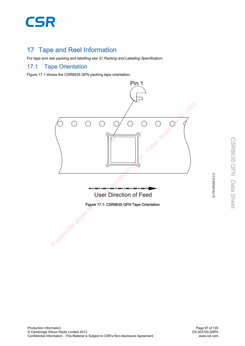
17 Tape and Reel InformationFor tape and reel packing and labelling see IC Packing and Labelling Specification.
17.1 Tape OrientationFigure 17.1 shows the CSR8635 QFN packing tape orientation.
G-T
W-0
0028
12.2
.2
User Direction of Feed
Pin 1
Figure 17.1: CSR8635 QFN Tape Orientation
Production Information© Cambridge Silicon Radio Limited 2013Confidential Information - This Material is Subject to CSR's Non-disclosure Agreement
Page 97 of 105CS-303725-DSP5
www.csr.com
CSR
8635 QFN D
ata Sheet
Prepa
red
for q
ingbo
keve
n.zh
ou -
exce
lpoint
.com
.cn -
Friday
, Sep
tem
ber 2
7, 2
013

17.2 Tape Dimensions
G-T
W-0
0028
11.3
.2
4.0See Note 1
12.0
0.25
R0.25
Bo
AoKo
1.75
2.0See Note 6
0.30 ± 0.05 A
A
Section A-A
7.5See Note 6
R0.3 MAX
±
A0 B0 K0 Unit Notes
8.30 8.30 1.10 mm
1. 10 sprocket hole pitch cumulative tolerance ±0.22. Camber not to exceed 1mm in 100mm3. Material: PS + C4. A0 and B0 measured as indicated5. K0 measured from a plane on the inside bottom of the
pocket to the top surface of the carrier6. Pocket position relative to sprocket hole measured
as true position of pocket, not pocket hole
Production Information© Cambridge Silicon Radio Limited 2013Confidential Information - This Material is Subject to CSR's Non-disclosure Agreement
Page 98 of 105CS-303725-DSP5
www.csr.com
CSR
8635 QFN D
ata Sheet
Prepa
red
for q
ingbo
keve
n.zh
ou -
exce
lpoint
.com
.cn -
Friday
, Sep
tem
ber 2
7, 2
013

17.3 Reel Information
G-T
W-0
0027
97.5
.2
102.02.0
330.02.0
W1(MEASURED AT HUB)
(MEASURED AT HUB)
"A"
ATTENTIONElectrostatic Sensitive Devices Safe Handling Required
W2
20.2
MIN
2.0 0.5
13.0+0.5-0.2
Detail "A"
Detail "B"
6 PS
PS
6
a(rim height)
88 REF
"b" REF
Figure 17.2: Reel Dimensions
Package TypeNominal Hub Width
(Tape Width)a b W1 W2 Max Units
8 x 8 x 0.9mmQFN
16 4.5 98.0 16.4(3.0/-0.2)
19.1 mm
17.4 Moisture Sensitivity LevelCSR8635 QFN is qualified to moisture sensitivity level MSL3 in accordance with JEDEC J-STD-020.
Production Information© Cambridge Silicon Radio Limited 2013Confidential Information - This Material is Subject to CSR's Non-disclosure Agreement
Page 99 of 105CS-303725-DSP5
www.csr.com
CSR
8635 QFN D
ata Sheet
Prepa
red
for q
ingbo
keve
n.zh
ou -
exce
lpoint
.com
.cn -
Friday
, Sep
tem
ber 2
7, 2
013

18 Document References
Document Reference, Date
BlueCore Audio API Specification CS-209064-DD
BlueTest User Guide CS-102736-UG
Bluetooth and USB Design Considerations CS-101412-AN
Core Specification of the Bluetooth System Bluetooth Specification Version 4.0, 17 December 2009
CSR8635 QFN Performance Specification CS-303738-SP
Electrostatic Discharge (ESD) Sensitivity Testing,Machine Model (MM) JESD22-A115C
ESDA/JEDEC Joint Standard For Electrostatic DischargeSensitivity Testing Human Body Model (HBM) -Component Level
ANSI/ESDA/JEDEC JS-001-201
Field-Induced Charged-Device Model Test Method forElectrostatic- Discharge-Withstand Thresholds ofMicroelectronic Components
JESD22-C101E
IC Packing and Labelling Specification CS-112584-SP
IEC 61000-4-2Electromagnetic compatibility (EMC) – Part 4-2: Testingand measurement techniques – Electrostatic dischargeimmunity test
IEC 61000-4-2, Edition 2.0, 2008-12
Kalimba Architecture 3 DSP User Guide CS-202067-UG
Lithium Polymer Battery Charger Calibration andOperation for CSR8670 CS-204572-AN
Moisture / Reflow Sensitivity Classification forNonhermitic Solid State Surface Mount Devices IPC / JEDEC J-STD-020
Optimising BlueCore5-Multimedia ADC PerformanceApplication Note CS-120059-AN
Selection of I²C EEPROMS for Use with BlueCore bcore-an-008P
Typical Solder Reflow Profile for Lead-free Device CS-116434-AN
Universal Serial Bus Specification v2.0, 27 April 2000
USB Battery Charging Specification v1.2 December 7th 2010, also errata and ECNs throughMarch 15th 2012
Production Information© Cambridge Silicon Radio Limited 2013Confidential Information - This Material is Subject to CSR's Non-disclosure Agreement
Page 100 of 105CS-303725-DSP5
www.csr.com
CSR
8635 QFN D
ata Sheet
Prepa
red
for q
ingbo
keve
n.zh
ou -
exce
lpoint
.com
.cn -
Friday
, Sep
tem
ber 2
7, 2
013

Terms and DefinitionsTerm Definition
8DPSK 8-phase Differential Phase Shift Keying
π/4 DQPSK π/4 rotated Differential Quaternary Phase Shift Keying
µ-law Audio companding standard (G.711)
A-law Audio companding standard (G.711)
A2DP Advanced Audio Distribution Profile
AAC Advanced Audio Coding
AC Alternating Current
ACL Asynchronous Connection-oriented
ADC Analogue to Digital Converter
AEC Acoustic Echo Cancellation
AFC Automatic Frequency Control
AFH Adaptive Frequency Hopping
AG Audio Gateway
AGC Automatic Gain Control
ALU Arithmetic Logic Unit
AVRCP Audio/Video Remote Control Profile
BCCMD BlueCore CoMmanD
BCSP BlueCore Serial Protocol
BEC Bit Error Concealment
BER Bit Error Rate
BFI Bad Frame Indicator
BIST Built-In Self-Test
BlueCore® Group term for CSR’s range of Bluetooth wireless technology ICs
Bluetooth® Set of technologies providing audio and data transfer over short-range radio connections
BMC Burst Mode Controller
CNG Comfort Noise Generation
codec Coder decoder
CRC Cyclic Redundancy Check
CSR Cambridge Silicon Radio
CTS Clear To Send
CVC Clear Voice Capture
Production Information© Cambridge Silicon Radio Limited 2013Confidential Information - This Material is Subject to CSR's Non-disclosure Agreement
Page 101 of 105CS-303725-DSP5
www.csr.com
CSR
8635 QFN D
ata Sheet
Prepa
red
for q
ingbo
keve
n.zh
ou -
exce
lpoint
.com
.cn -
Friday
, Sep
tem
ber 2
7, 2
013

Term Definition
CVSD Continuously Variable Slope Delta Modulation
DAC Digital to Analogue Converter
DC Direct Current
DDS Direct Digital Synthesis
DI Device Id profile
DMA Direct Memory Access
DNL Differential Non Linearity (ADC accuracy parameter)
DSP Digital Signal Processor (or Processing)
DUT Device Under Test
e.g. exempli gratia, for example
EDR Enhanced Data Rate
EEPROM Electrically Erasable Programmable Read Only Memory
EIA Electronic Industries Alliance
EMC ElectroMagnetic Compatibility
EQ EQualiser
eSCO extended SCO
ESD Electrostatic Discharge
ESR Equivalent Series Resistance
etc et cetera, and the rest, and so forth
FIR Finite Impulse Response (filter)
FSK Frequency Shift Keying
G.722 An ITU-T standard wideband speech codec operating at 48, 56 and 64 kbps
GCI General Circuit Interface
GSM Global System for Mobile communications
GUI Graphical User Interface
H4DS H4 Deep Sleep
HBM Human Body Model
HCI Host Controller Interface
HFP Hands-Free Profile
HSP HeadSet Profile
I²C Inter-Integrated Circuit Interface
I²S Inter-Integrated Circuit Sound
i.e. Id est, that is
Production Information© Cambridge Silicon Radio Limited 2013Confidential Information - This Material is Subject to CSR's Non-disclosure Agreement
Page 102 of 105CS-303725-DSP5
www.csr.com
CSR
8635 QFN D
ata Sheet
Prepa
red
for q
ingbo
keve
n.zh
ou -
exce
lpoint
.com
.cn -
Friday
, Sep
tem
ber 2
7, 2
013

Term Definition
I/O Input/Output
IC Integrated Circuit
IF Intermediate Frequency
IIR Infinite Impulse Response (filter)
INL Integral Non-Linearity (ADC accuracy parameter)
IPC See www.ipc.org
IPM Intelligent Power Management
IQ In-Phase and Quadrature
ISDN Integrated Services Digital Network
JEDEC Joint Electron Device Engineering Council (now the JEDEC Solid State Technology Association)
Kalimba An open platform DSP co-processor, enabling support of enhanced audio applications, such asecho and noise suppression and file compression / decompression
Kb Kilobit
LC An inductor (L) and capacitor (C) network
LDO Low (voltage) Drop-Out
LED Light-Emitting Diode
LM Link Manager
LNA Low Noise Amplifier
LSB Least Significant Bit (or Byte)
MAC Multiplier and ACcumulator
Mb Megabit
MCU MicroController Unit
MIPS Million Instructions Per Second
MISO Master In Slave Out
MLC MultiLayer Ceramic
MMU Memory Management Unit
MP3 MPEG-1 audio layer 3
mSBC modified Sub-Band Coding
N/A Not Applicable
NDVC Noise Dependent Volume Control
NSMD Non-Solder Mask Defined
PA Power Amplifier
PC Personal Computer
PCB Printed Circuit Board
Production Information© Cambridge Silicon Radio Limited 2013Confidential Information - This Material is Subject to CSR's Non-disclosure Agreement
Page 103 of 105CS-303725-DSP5
www.csr.com
CSR
8635 QFN D
ata Sheet
Prepa
red
for q
ingbo
keve
n.zh
ou -
exce
lpoint
.com
.cn -
Friday
, Sep
tem
ber 2
7, 2
013
Term Definition
PCM Pulse Code Modulation
PIN Personal Identification Number
PIO Parallel Input/Output
PIO Programmable Input/Output, also known as general purpose I/O
PLC Packet Loss Concealment
plc public limited company
PS Key Persistent Store Key
PWM Pulse Width Modulation
QFN Quad-Flat No-lead
RAM Random Access Memory
RC A Resistor and Capacitor network
RF Radio Frequency
RGB Red Green Blue
RISC Reduced Instruction Set Computer
RoHS Restriction of Hazardous Substances in Electrical and Electronic Equipment Directive (2002/95/EC)
ROM Read Only Memory
RSSI Received Signal Strength Indication
RTS Request To Send
RX Receive or Receiver
SBC Sub-Band Coding
SCL Serial Clock Line
SCMS Serial Copy Management System (SCMS-T). A content protection scheme for secure transportand use of compressed digital music
SCO Synchronous Connection-Oriented
SDA Serial DAta (line)
SIG (Bluetooth) Special Interest Group
SLC Service Level Connection
SMPS Switch-Mode Power Supply
SNR Signal-to-Noise Ratio
SPI Serial Peripheral Interface
TBD To Be Defined
TCXO Temperature Compensated crystal Oscillator
THD+N Total Harmonic Distortion and Noise
Production Information© Cambridge Silicon Radio Limited 2013Confidential Information - This Material is Subject to CSR's Non-disclosure Agreement
Page 104 of 105CS-303725-DSP5
www.csr.com
CSR
8635 QFN D
ata Sheet
Prepa
red
for q
ingbo
keve
n.zh
ou -
exce
lpoint
.com
.cn -
Friday
, Sep
tem
ber 2
7, 2
013

Term Definition
TX Transmit or Transmitter
UART Universal Asynchronous Receiver Transmitter
UI User Interface
USB Universal Serial Bus
VCO Voltage Controlled Oscillator
VM Virtual Machine
VoIP Voice over Internet Protocol
W-CDMA Wideband Code Division Multiple Access
Wi-Fi® Wireless Fidelity (IEEE 802.11 wireless networking)
WNR Wind Noise Reduction
Production Information© Cambridge Silicon Radio Limited 2013Confidential Information - This Material is Subject to CSR's Non-disclosure Agreement
Page 105 of 105CS-303725-DSP5
www.csr.com
CSR
8635 QFN D
ata Sheet
Prepa
red
for q
ingbo
keve
n.zh
ou -
exce
lpoint
.com
.cn -
Friday
, Sep
tem
ber 2
7, 2
013