Features and Benefits - 13280136.s21i.faiusr.com
4
Rev. 1.02 8 Hall-effect sensor is a temperature stable, stress sensor. Superior high-temperature performance is made possible through a dynamic offset cancellation that utilizes chopper-stabilization. This method reduces the offset voltage normally caused by device over molding, temperature dependencies, and thermal stress. 8 includes the following on a single silicon chip: voltage regulator, Hall voltage generator, small-signal amplifier, chopper stabilization, Schmitt trigger, Advanced DMOS wafer fabrication processing is used to take advantage of low-voltage requirements, component matching, very low input-offset errors, and small component geometries. This device requires the presence of both south and north polarity magnetic fields for operation. In the presence of a south polarity field of sufficient strength, the device output sensor on, and only switches off when a north polarity field of sufficient strength is present. 8 is rated for operation between the ambient temperatures –40℃ and 85℃ for the E temperature range, and –40℃ to 125℃ for the K temperature range. The two package styles available provide magnetically optimized solutions for most applications. Package SO is an SOT-23, a miniature low-profile surface-mount package, while package UA is a three-lead ultra mini SIP for through-hole mounting. Packages is Halogen Free standard and which have been verified by third party lab. Features and Benefits DMOS Hall IC Technology. Reverse bias protection on power supply pin. Chopper stabilized amplifier stage. Optimized for BLDC motor applications. Reliable and low shifting on high Temp condition. Good ESD Protection. 100% tested at 125 ℃ for K. Custom sensitivity / Temperature selection are available. Applications High temperature Fan motor 3 phase BLDC motor application Speed sensing Position sensing Current sensing Revolution counting Solid-State Switch Linear Position Detection Angular Position Detection Proximity Detection High ESD Capability DH18 DH18 DH18 DH18 网址:http://www.hall-wafer.com 地址:深圳市龙岗区龙西清水路务地埔龙昌10楼1001 电话:0755-84821761 13430722511
Transcript of Features and Benefits - 13280136.s21i.faiusr.com

Rev. 1.02
8 Hall-effect sensor is a temperature stable, stress sensor. Superior high-temperature performance is made possible through a dynamic offset cancellation that utilizes chopper-stabilization. This method reduces the offset voltage normally caused by device over molding, temperature dependencies, and thermal stress.
8 includes the following on a single silicon chip: voltage regulator, Hall voltage
generator, small-signal amplifier, chopper stabilization, Schmitt trigger, Advanced DMOS wafer fabrication processing is used to take advantage of low-voltage requirements, component matching, very low input-offset errors, and small component geometries.
This device requires the presence of both south and north polarity magnetic fields for
operation. In the presence of a south polarity field of sufficient strength, the device output sensor on, and only switches off when a north polarity field of sufficient strength is present.
8 is rated for operation between the ambient temperatures –40℃ and 85℃ for the
E temperature range, and –40℃ to 125℃ for the K temperature range. The two package styles available provide magnetically optimized solutions for most applications. Package SO is an SOT-23, a miniature low-profile surface-mount package, while package UA is a three-lead ultra mini SIP for through-hole mounting.
Packages is Halogen Free standard and which have been verified by third party lab.
Features and Benefits DMOS Hall IC Technology. Reverse bias protection on power supply pin. Chopper stabilized amplifier stage. Optimized for BLDC motor applications. Reliable and low shifting on high Temp condition. Good ESD Protection. 100% tested at 125 ℃ for K. Custom sensitivity / Temperature selection are available.
Applications High temperature Fan motor 3 phase BLDC motor application Speed sensing Position sensing Current sensing Revolution counting Solid-State Switch Linear Position Detection Angular Position Detection Proximity Detection High ESD Capability
DH18
DH18
DH18DH18
网址:http://www.hall-wafer.com
地址:深圳市龙岗区龙西清水路务地埔龙昌10楼1001
电话:0755-84821761 13430722511

Rev. 1.02
Functional Diagram
VoltageRegulator
Amp
VDD Out
GND
Hall SensorHall
Sensor Clock
Absolute Maximum Ratings At (Ta=25℃)
Characteristics Values Unit Supply voltage, (VDD) 28 V Output Voltage,(Vout) 28 V Reverse voltage, (VDD) -28 V Magnetic flux density Unlimited Gauss
Output current, (Iout) 50 mA
Operating Temperature Range, (Ta) “E” version -40 to +85 ℃ “K” version -40 to +125 ℃
Storage temperature range, (Ts) -65 to +150 °C Maximum Junction Temp,(Tj) 150 °C
Thermal Resistance (θja) UA / SO 206 / 543 ℃/W (θjc) UA / SO 148 / 410 ℃/W
Package Power Dissipation, (PD) UA / SO 606 / 230 mW Note: Do not apply reverse voltage to VDD and VOUT Pin, It may be caused for Miss function or damaged device.
网址:http://www.hall-wafer.com
地址:深圳市龙岗区龙西清水路务地埔龙昌10楼1001
电话:0755-84821761 13430722511

Rev. 1.02
Electrical Specifications DC Operating Parameters: TA=+25℃, VDD=12V
Parameters Test Conditions Min Typ Max Units Supply Voltage,(VDD) Operating 2.5 24.0 V
Supply Current,(IDD) B<BOP 5.0 mA
Output Saturation Voltage, (Vsat) Iout=20mA,B>BOP 400.0 mV
Output Leakage Current, (Ioff) IOFF B<BRP, VOUT = 12V 10.0 uA Internal Oscillator Chopper Frequency,(fOSC) 69 kHz
Output Rise Time, (TR) RL=1.1KΩ, CL =20pF 0.04 0.45 uS Output Fall Time, (TF) RL=820Ω; CL =20pF 0.18 0.45 uS
Electro-Static Discharge HBM 4 KV
Operate Point,(BOP) UA(SO) 5(-25) 25(-5) Gauss
Release Point,(BRP) UA(SO) -25(5) -5(25) Gauss
Hysteresis,(BHYS) 30 Gauss
Typical application circuit
C1188
Vcc
R
C2
VDD(1)
Out(3)
Gnd(2)
Output
R:1KΩ C1:10nF C2:1nF
DH
网址:http://www.hall-wafer.com
地址:深圳市龙岗区龙西清水路务地埔龙昌10楼1001
电话:0755-84821761 13430722511
Rev. 1.02
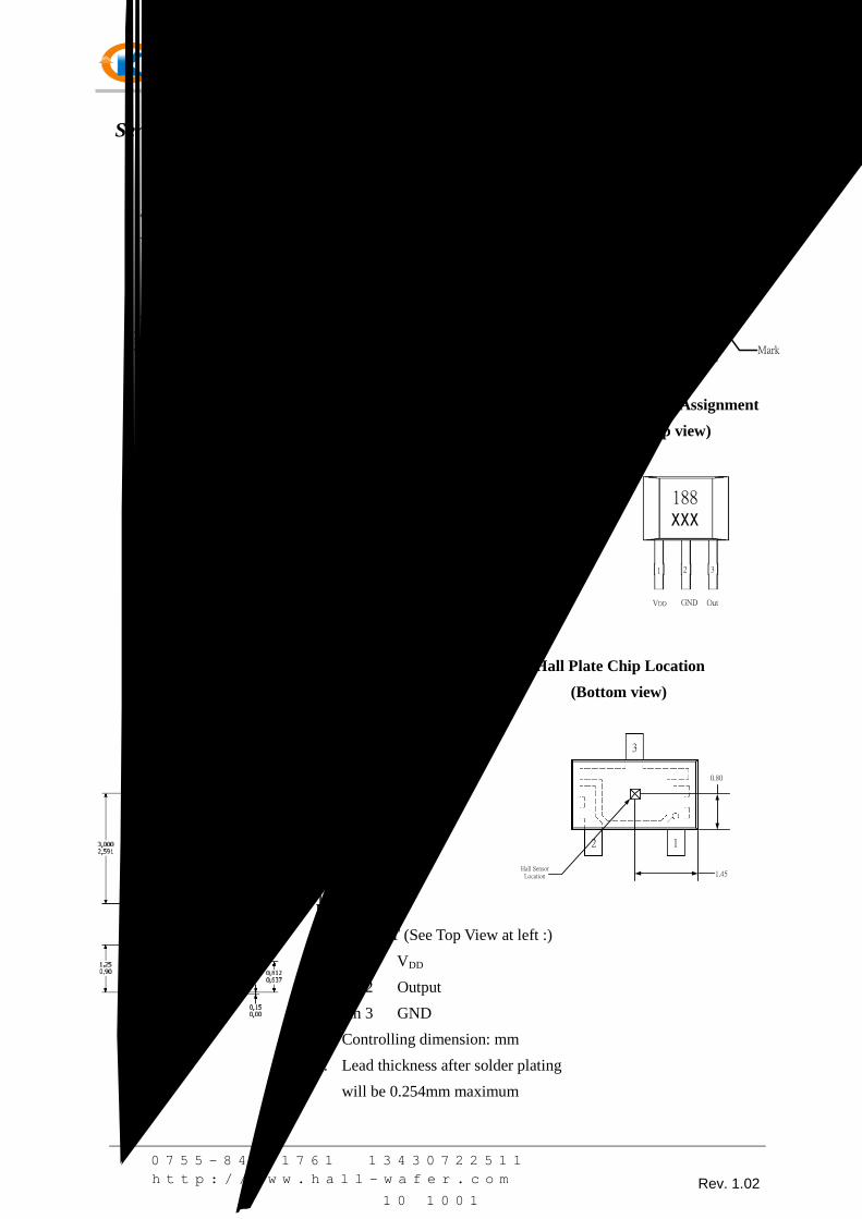
SO Package Hall Plate Chip Location (Top View) (Bottom view)
188XX
1 2
3
NOTES:
1. PINOUT (See Top View at left :) Pin 1 VDD Pin 2 Output Pin 3 GND
2. Controlling dimension: mm 3. Lead thickness after solder plating
will be 0.254mm maximum
0.80
1.45Hall Sensor
Location
12
3
Sensor Location, Package Dimension and Marking
Package UA Package Hall Chip location
188XXX
NOTES: 1).Controlling dimension: mm 2).Leads must be free of flash and plating voids 3).Do not bend leads within 1
mm of lead to package interface.
4).PINOUT: Pin 1 VDD Pin 2 GND Pin 3 Output
Output Pin Assignment (Top view)
1 2 3
VDD GND Out
188
XXX
0.9
2.00
Hall SensorLocation
Mark
网址:http://www.hall-wafer.com
地址:深圳市龙岗区龙西清水路务地埔龙昌10楼1001
电话:0755-84821761 13430722511