FCBGA Package Warpage Definition Stage Project Raiyo Aspandiar – INTEL HDP User Group Member...
26
FCBGA Package Warpage Definition Stage Project Raiyo Aspandiar – INTEL HDP User Group Member Meeting Host: Shengyi Technology Co., Ltd. And NERCECBM Guangdong, China December 5, 2012 Presented by Brian Smith © HDP User Group International, Inc. 1
-
Upload
bethanie-lawson -
Category
Documents
-
view
235 -
download
5
Transcript of FCBGA Package Warpage Definition Stage Project Raiyo Aspandiar – INTEL HDP User Group Member...

FCBGA Package Warpage Definition Stage Project
Raiyo Aspandiar – INTEL
HDP User Group Member MeetingHost: Shengyi Technology Co., Ltd.
And NERCECBMGuangdong, China
December 5, 2012Presented by Brian Smith
© HDP User Group International, Inc. 1

© HDP User Group International, Inc. 2
Purpose

© HDP User Group International, Inc. 3
Background
Package/board Warpage increasing trends •Driven by thinner package substrates and thinner die
Package/Board contacts getting smaller and closer
thereby reducing ability to overcome increased Warpage. Solder Joint Quality Impact of increasing Package
and Warpage.
With advent of lead free soldering, the assembly temperatures have increased and the warpage impact has been exacerbated.

© HDP User Group International, Inc. 4
Examples of Warpage Induced Defects
for Area Array Solder Joints
Stretched joint
Head on pillow
Head-on-Pillow Open
Die
Board
Non –Wet Open
Various Solder Joint Defects can occur during SMT Reflow Soldering due to Excessive BGA component and/or Board Warpage

© HDP User Group International, Inc. 5
Real Time Video of FCBGA Solder Joint Mechanism in Assembly Line Reflow Oven

© HDP User Group International, Inc. 6
Project Scope
- What is IN the Scope
Die
Package Substrate
Printed Circuit Board
Project Focus Area
FC BGA Package Substrate
Solder Paste Rheology Wetting Metallurgy Activator chemistry Volume printed on land
Package Termination Geometry (ball, pillar, column, etc) Metallurgy (SAC, low Ag SAC, BiSnAg, other)
FCBGA Package just as its entering the SMT Reflow Oven
Reflow Process Temperature –Time Profile Oven Atmosphere
Surface Finish OSP/ENIG/
ImAg/ENEPIG/ etc

© HDP User Group International, Inc. 7
Project Scope
Die
Package Substrate
Printed Circuit Board
FC BGA Package Substrate
Package Warpage Mitigation Laminate Type Stack-up Die Thickness Die Size
- What is OUT of the Scope
Package Warpage Measurement Metrologies Specifications
Board Warpage Mitigation Laminate Type Stack-up
Board Warpage Measurement Metrologies Specifications

Objective
8© HDP User Group International, Inc.
Establish a limit for dynamic package warpage
that can be mitigated during board assembly
without impacting solder joint quality

9
Project Goals
• Identify mitigation paths for solder joint yield loss caused during the SMT reflow soldering process specifically due to the excessive warpage of package and/or boards
• Evaluate these mitigation paths for their effectiveness in increasing solder joint yield despite high levels of package and/or board warpage
© HDP User Group International, Inc.
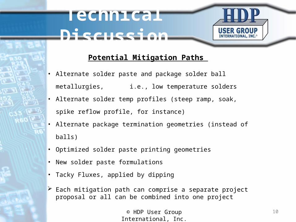
Technical Discussion
Potential Mitigation Paths
• Alternate solder paste and package solder ball metallurgies,
i.e., low temperature solders
• Alternate solder temp profiles (steep ramp, soak, spike reflow
profile, for instance)
• Alternate package termination geometries (instead of balls)
• Optimized solder paste printing geometries
• New solder paste formulations
• Tacky Fluxes, applied by dipping
Each mitigation path can comprise a separate project proposal or all can be combined into one project
10© HDP User Group International, Inc.
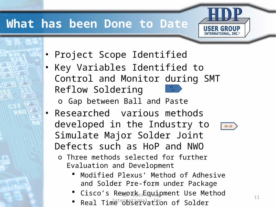
What has been Done to Date
• Project Scope Identified• Key Variables Identified to Control and Monitor
during SMT Reflow Solderingo Gap between Ball and Paste
• Researched various methods developed in the Industry to Simulate Major Solder Joint Defects such as HoP and NWOo Three methods selected for further Evaluation and
Development Modified Plexus’ Method of Adhesive and Solder Pre-
form under Package Cisco’s Rework Equipment Use Method Real Time observation of Solder Joint Formation
within in-line reflow oven© HDP User Group International, Inc. 11
15 -17
18-25

What is Planned For the Future
• Develop Metrology: Explore the feasibility of using Cisco Rework Method and Modified Plexus Adhesive Method for use with a full array package instead of a single solder ball at a time
• Develop Real Time Monitoring: Explore possibility of using real time monitoring of solder joint formation within reflow oven with high dynamic warpage components, and subsequently characterize the dynamic warpage of problematic packages already in use today
• Brainstorm Mitigation paths: for excessive warpage of package and/or boards induced SMT solder joint yield loss and select potential candidates for assessment
• Select Mitigation Path: Obtain Components and Design and Procure Boards for Evaluation of Mitigation Paths
• Assess Effectiveness of Mitigation Path: Design and Run Experiments to evaluate present capability of materials and processes and feasibility of the Warpage-induced Defects’ Mitigation Paths
© HDP User Group International, Inc. 12
© HDP User Group International, Inc. 13
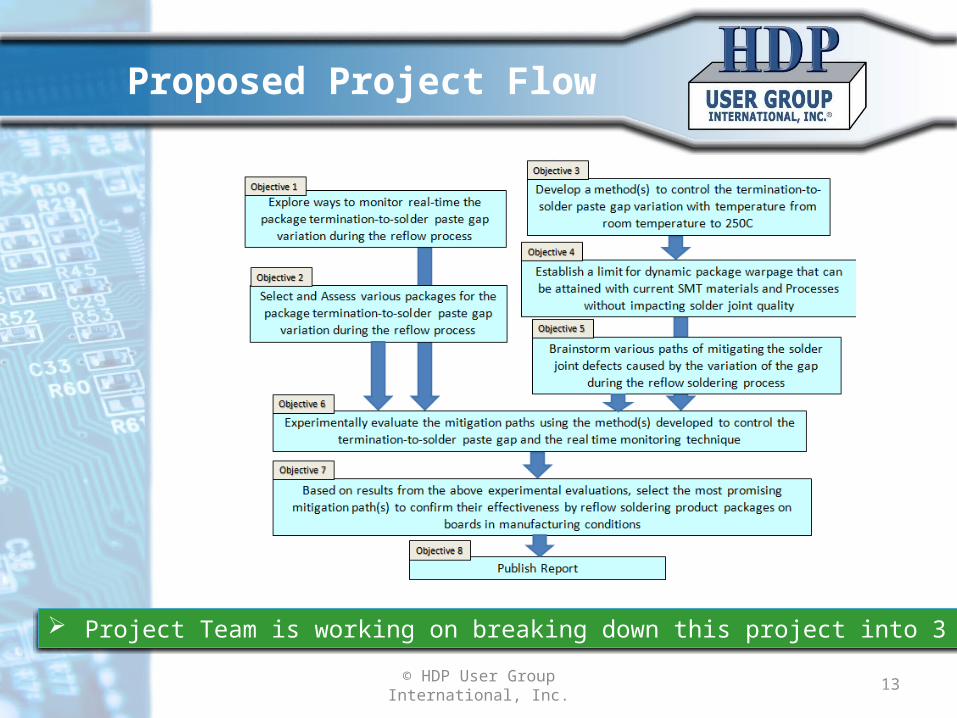
Proposed Project Flow
Project Team is working on breaking down this project into 3 Phases

© HDP User Group International, Inc. 14
Team Members –to date
• Akrometrix
• Alcatel-Lucent
• Arlon
• ASE
• Celestica
• Ciena
• Cisco
• Curtiss-Wright
• Ericsson
• Flextronics
• Fujitsu
• Hitachi
• Hitachi-Chemical
• IBM
• Intel
• IST Group
• Juniper
• Multek
• Nihon-Superior
• Panasonic
• Phillips
• Plexus
• Rockwell
• Shengyi
• TTM Tech
• Ventec

Back-up
© HDP User Group International, Inc. 15
Temp
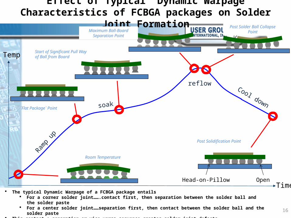
Effect of Typical Dynamic Warpage Characteristics of FCBGA packages on Solder Joint Formation
© HDP User Group International, Inc.16
Head-on-Pillow Open
Room Temperature
`Flat Package` Point
Start of Significant Pull Way of Ball from Board
Maximum Ball-Board Separation Point
Post Solder Ball Collapse Point
Post Solidification Point
Time
Ramp
up
soak
reflowCool down
The typical Dynamic Warpage of a FCBGA package entails For a corner solder joint…….contact first, then separation between the solder ball and the solder paste For a center solder joint……separation first, then contact between the solder ball and the solder paste
This contact + separation or vice versa sequence creates solder joint defects
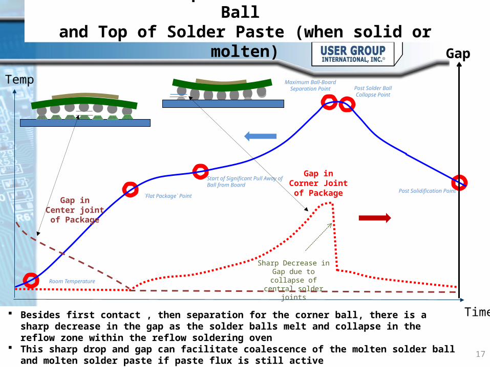
Variation of Gap between Bottom of Solder Ball and Top of Solder Paste (when solid or molten)
© HDP User Group International, Inc. 17
Time
`Flat Package` Point
Start of Significant Pull Away of Ball from Board
Temp Maximum Ball-Board Separation Point Post Solder Ball
Collapse Point
Post Solidification PointGap in Center
joint of Package
Gap in Corner Joint of Package
Gap
Room Temperature
Sharp Decrease in Gap due to collapse of central
solder joints
Besides first contact , then separation for the corner ball, there is a sharp decrease in the gap as the solder balls melt and collapse in the reflow zone within the reflow soldering oven
This sharp drop and gap can facilitate coalescence of the molten solder ball and molten solder paste if paste flux is still active

Key Points
Any method of simulating BGA package warpage during reflow soldering needs to address the following to simulate the conditions for corner solder joints
Initial Contact of the BGA solder ball with the solder paste and subsequent separation before or during the soak zone or ramp regionSharp drop in the gap between the molten solder ball and molten paste when the solder balls melt and collapse in the reflow zone region
Any method of simulating BGA package warpage during reflow soldering needs to address the following to simulate the conditions for central solder joints
No contact between the BGA solder ball and solder paste before or during the ramp zone or soak zone until the flat package point is reachedContact developed between the solder ball and solder paste later in the soak zone
© HDP User Group International, Inc. 18
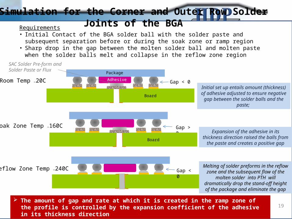
Simulation for the Corner and Outer Row Solder Joints of the BGA
© HDP User Group International, Inc. 19
Requirements• Initial Contact of the BGA solder ball with the solder paste and subsequent separation before
or during the soak zone or ramp region• Sharp drop in the gap between the molten solder ball and molten paste when the solder balls
melt and collapse in the reflow zone region
Gap < 0
Package
Adhesive
Board
Gap > 0
Room Temp ~20C
Soak Zone Temp ~160C
Board
Board
Reflow Zone Temp ~240C Gap < 0
Initial set up entails amount (thickness) of adhesive adjusted to ensure negative
gap between the solder balls and the paste;
SAC Solder Pre-form and Solder Paste or Flux
Expansion of the adhesive in its thickness direction raised the balls from
the paste and creates a positive gap
Melting of solder preforms in the reflow zone and the subsequent flow of the
molten solder into PTH will dramatically drop the stand-off height of
the package and eliminate the gap
The amount of gap and rate at which it is created in the ramp zone of the profile is controlled by the expansion coefficient of the adhesive in its thickness direction
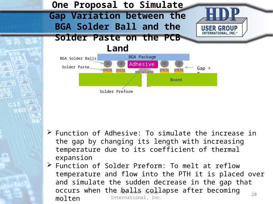
One Proposal to Simulate Gap Variation between the BGA Solder Ball and the Solder Paste on the PCB Land
© HDP User Group International, Inc. 20
Gap > 0
Board
Adhesive
Solder Preform
BGA PackageBGA Solder Balls
Solder Paste
Function of Adhesive: To simulate the increase in the gap by changing its length with increasing temperature due to its coefficient of thermal expansion
Function of Solder Preform: To melt at reflow temperature and flow into the PTH it is placed over and simulate the sudden decrease in the gap that occurs when the balls collapse after becoming molten

Simulation for the Central Solder Joints of the BGA
Gap < 0
When the low temp solder pre-form melts balls lowered and touch SAC
solder paste
Balls and solder paste melt while in contact
Gap at RT > 0
Gap < 0
Package
Adhesive
Room Temp ~20C
Soak Zone Temp ~160C
Reflow Zone Temp ~240C
Low Temp Solder Pre-form and Solder Paste or Flux Initial set up entails a gap between the
solder balls and the paste; gap amount controlled by amount (thickness) of
adhesive
Requirements• No contact between the BGA solder ball and solder paste before or during the
ramp zone or soak zone until the flat package point is reached• Contact developed between the solder ball and solder paste later in the soak zone
The temperature at which the solder ball and paste make contact can be varied by using different solders with different melting points in the SAC profile soak zone
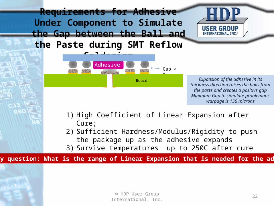
Requirements for Adhesive Under Component to Simulate the Gap between the Ball and the Paste during SMT Reflow
Soldering
© HDP User Group International, Inc. 22
Gap > 0
Board Expansion of the adhesive in its thickness direction raises the balls from
the paste and creates a positive gapMinimum Gap to simulate problematic
warpage is 150 microns
Adhesive
1) High Coefficient of Linear Expansion after Cure; 2) Sufficient Hardness/Modulus/Rigidity to push the package up
as the adhesive expands3) Survive temperatures up to 250C after cure4) Dispensable or screen printable
Key question: What is the range of Linear Expansion that is needed for the adhesive?

Cisco’s SRT Rework Equipment Method for Head-on-Pillow Testing
© HDP User Group International, Inc. 23
BGA rework equipment was also used to reflow the solder ball and the solder paste, while controlling the movement of the solder ball with respect to the solder paste on the pad.
The purpose of controlling the movement is to mimic the movement of the corner balls of a BGA as they warp during the reflow process.

Conditions for Cisco’s Method
© HDP User Group International, Inc. 24
C1
C2
C1: Initially there is no initial contact between the solder ball and the paste. Then at 200 ° C during the cooling down phase, the solder ball is pulled down slowly (1 mil/second) so that it makes contact with the solder paste.
C2: Initially there is no initial contact between the solder ball and paste. Then at 190 °C during the cooling down phase, the solder ball is pulled down slowly so that it makes contact with the solder paste. This condition is similar to C1 but there is less contact timebefore solidification.
Note: When initial contact is made between ball and paste, no H-o-P defects were formed

Photo’s of Cisco’s Method for Evaluating H-o-P defects
© HDP User Group International, Inc. 25
Before Solder Paste Reflow After Solder Paste Reflow
Aspects of Actual Reflow Soldering of high warpage BGAs NOT Simulated in this Test Lifting up of the solder ball from the solder paste during initial temperature
ramp (though this can be done with the equipment) Un-constrained Ball Collapse when the solder melts Temperature Profile simulated with hot air rework machine instead of a
reflow oven
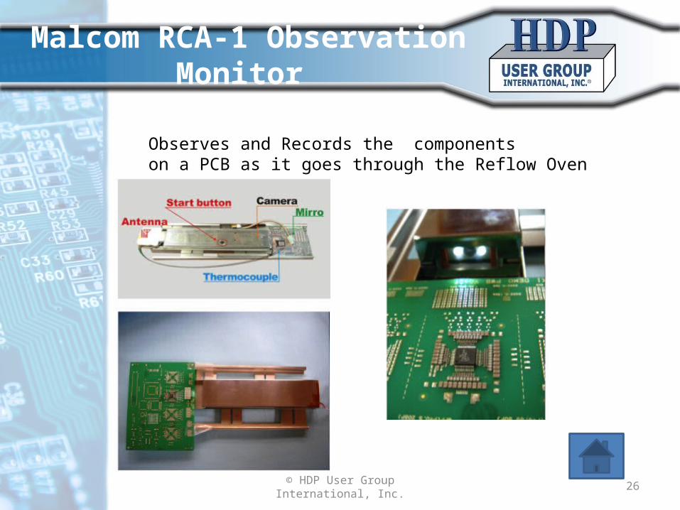
Malcom RCA-1 Observation Monitor
© HDP User Group International, Inc. 26
Observes and Records the components on a PCB as it goes through the Reflow Oven