Fazal Ahmad Khalid - Abdus Salam Centre for Physics Fazal Ahmad Khalid Pro-Rector GIK Institute of...
12
1 Fazal Ahmad Khalid Pro-Rector GIK Institute of Engineering Sciences and Technology Topi, NWFP, Pakistan ([email protected]) Workshop on Nanoscience and Catalysts 24-25 March 2008, QAU, Islamabad Nanocomposites for Thermal management Applications
Transcript of Fazal Ahmad Khalid - Abdus Salam Centre for Physics Fazal Ahmad Khalid Pro-Rector GIK Institute of...
1
Fazal Ahmad KhalidPro-Rector
GIK Institute of Engineering Sciences and TechnologyTopi, NWFP, Pakistan
Workshop on Nanoscience and Catalysts 24-25 March 2008, QAU, Islamabad
Nanocomposites forThermal management
Applications
2
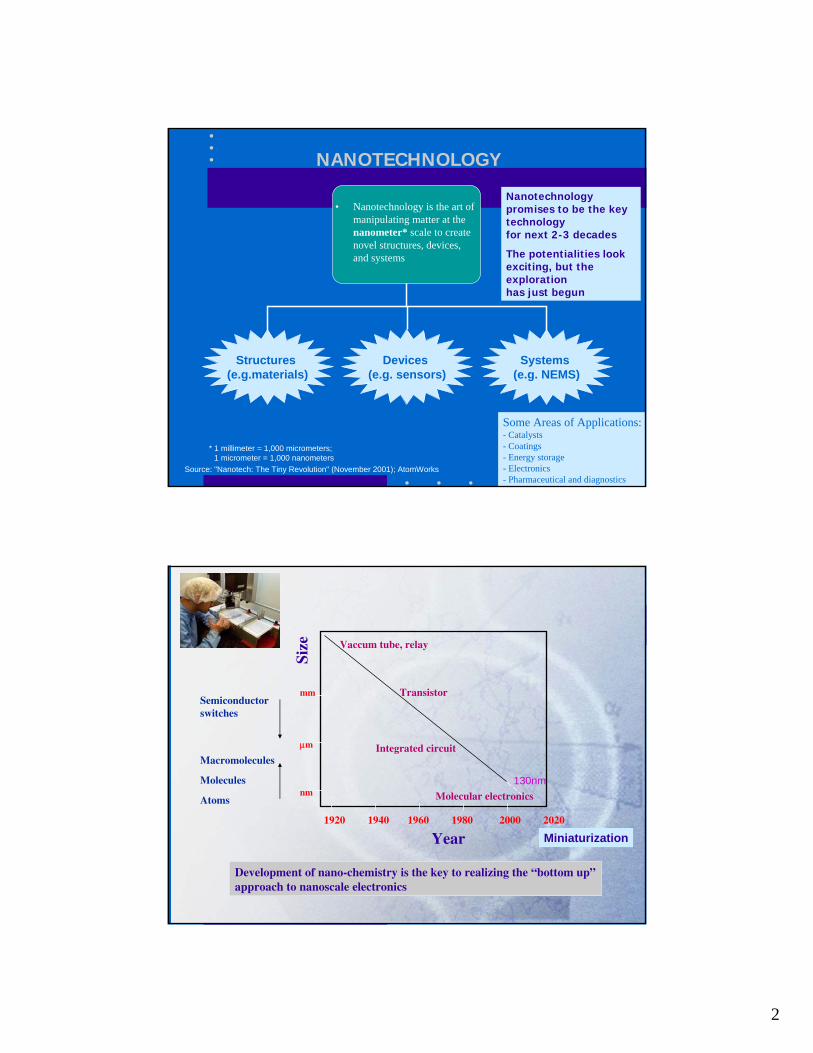
NANOTECHNOLOGY
* 1 millimeter = 1,000 micrometers; 1 micrometer = 1,000 nanometers
Source: "Nanotech: The Tiny Revolution" (November 2001); AtomWorks
• Nanotechnology is the art of manipulating matter at the nanometer* scale to create novel structures, devices, and systems
Structures (e.g.materials)
Devices (e.g. sensors)
Systems (e.g. NEMS)
Some Areas of Applications:- Catalysts- Coatings- Energy storage- Electronics- Pharmaceutical and diagnostics
Nanotechnology promises to be the key technology for next 2-3 decades
The potentialities look exciting, but the exploration has just begun
Size
Semiconductorswitches
Macromolecules
Molecules
Atomsnm
μm
mm
Year1920 1940 1960 1980 2000 2020
Vaccum tube, relay
Transistor
Integrated circuit
Molecular electronics
Development of nano-chemistry is the key to realizing the “bottom up”approach to nanoscale electronics
130nm
Miniaturization
3
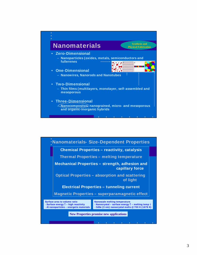
Nanomaterials• Zero-Dimensional
– Nanoparticles (oxides, metals, semiconductors and fullerenes
• One-Dimensional– Nanowires, Nanorods and Nanotubes
• Two-Dimensional– Thin films (multilayers, monolayer, self-assembled and
mesoporous
• Three-Dimensional– Nanocomposites, nanograined, micro- and mesoporous
and organic-inorganic hybrids
Synthesis andPhysical Fabrication
Nanomaterials- Size-Dependent Properties
Chemical Properties – reactivity, catalysis
Thermal Properties – melting temperature
Mechanical Properties – strength, adhesion andcapillary force
Optical Properties – absorption and scattering of light
Electrical Properties – tunneling current
Magnetic Properties – superparamagnetic effect
New Properties promise new applications
Surface area to volume ratio- Surface energy ⇑ – high reactivity- Al nanoparticles – energetic materials
Nanoscale melting temperature- Nanocrystal – surface energy ⇑ – melting temp ↓- CdSe (3 nm) nanocrystal melts @ 700 K (1678 K)
4
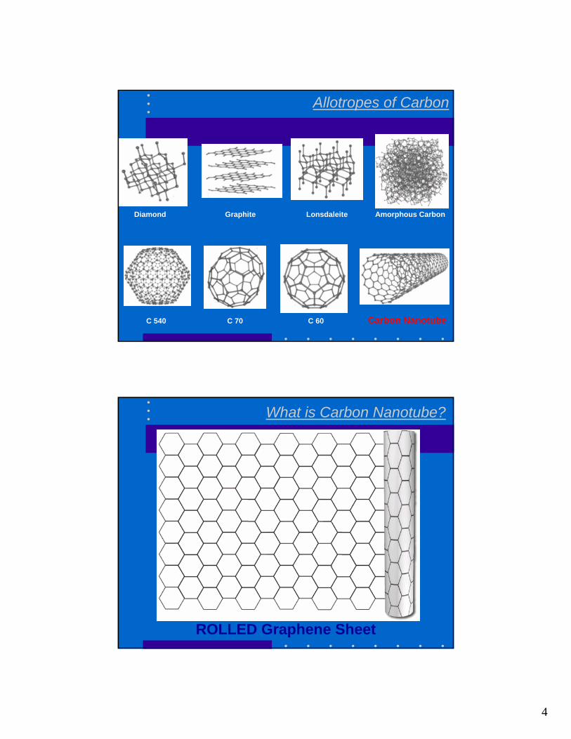
Allotropes of Carbon
C 540 C 70 C 60 Carbon Nanotube
Diamond Graphite Lonsdaleite Amorphous Carbon
What is Carbon Nanotube?
ROLLED Graphene Sheet
5
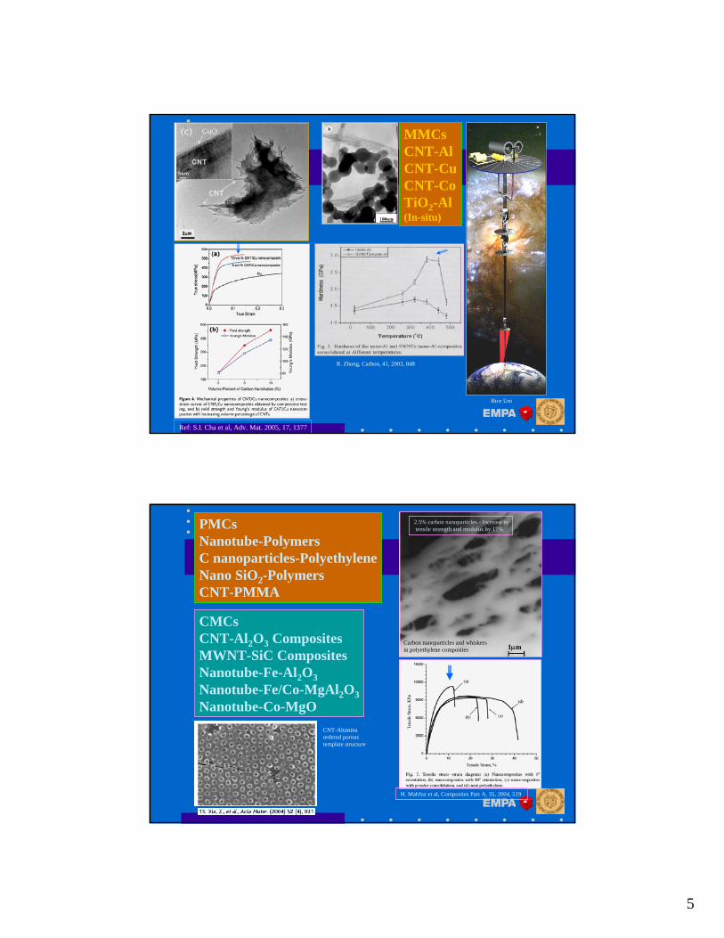
Ref: S.I. Cha et al, Adv. Mat. 2005, 17, 1377
Rice Uni
R. Zhong, Carbon, 41, 2003, 848
MMCsCNT-AlCNT-CuCNT-CoTiO2-Al(In-situ)
1μmCarbon nanoparticles and whiskersin polyethylene composites
2.5% carbon nanoparticles - Increase intensile strength and modulus by 17%
H. Mahfuz et al, Composites Part A, 35, 2004, 519
CMCsCNT-Al2O3 CompositesMWNT-SiC CompositesNanotube-Fe-Al2O3Nanotube-Fe/Co-MgAl2O3Nanotube-Co-MgO
PMCsNanotube-PolymersC nanoparticles-PolyethyleneNano SiO2-PolymersCNT-PMMA
CNT-Aluminaordered poroustemplate structure

6
Composite Materials
Engineering
Wind energy
Transport Auto- and LocomotivesNaval &Aircrafts
Sports
SpaceDefense
Bridges StructuresBuildingsMMCs
PMCsCMCs
NanoComposites – engineering, multifunctional, biomedical and construction
“Thermal management is one of the Key concerns in diverse fields such as Microelectronics and Space Technology”ExtreMat Project
ExtreMat shall push forward the limits in materials technology and will provide
and industrialize new knowledge based materials and compoundsfor to-end and new applications in
extreme environments
New Materials with enhanced
thermal conductivity
Approach to transfer the attractive physical propertiesof diamond to bulk engineering components
Insight toprocessing andcharacterization
of new compositematerials
7
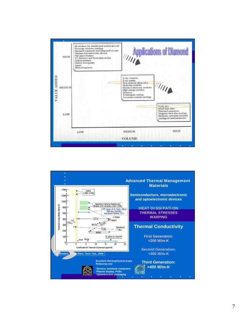
C. Zweben, Power Elect. Tech. Feb., 2006
Advanced Thermal Management Materials
Semiconductors, microelectronicand optoelectronic devices
HEAT DISSIPATIONTHERMAL STRESSES
WARPING
Thermal Conductivity
First Generation:<200 W/m-K
Second Generation:<400 W/m-K
Third Generation:>400 W/m-K
Excellent thermophysical propsReducing cost
-Servers, notebook computers-Plasma display, PCBs-Optoelectronic packaging
8
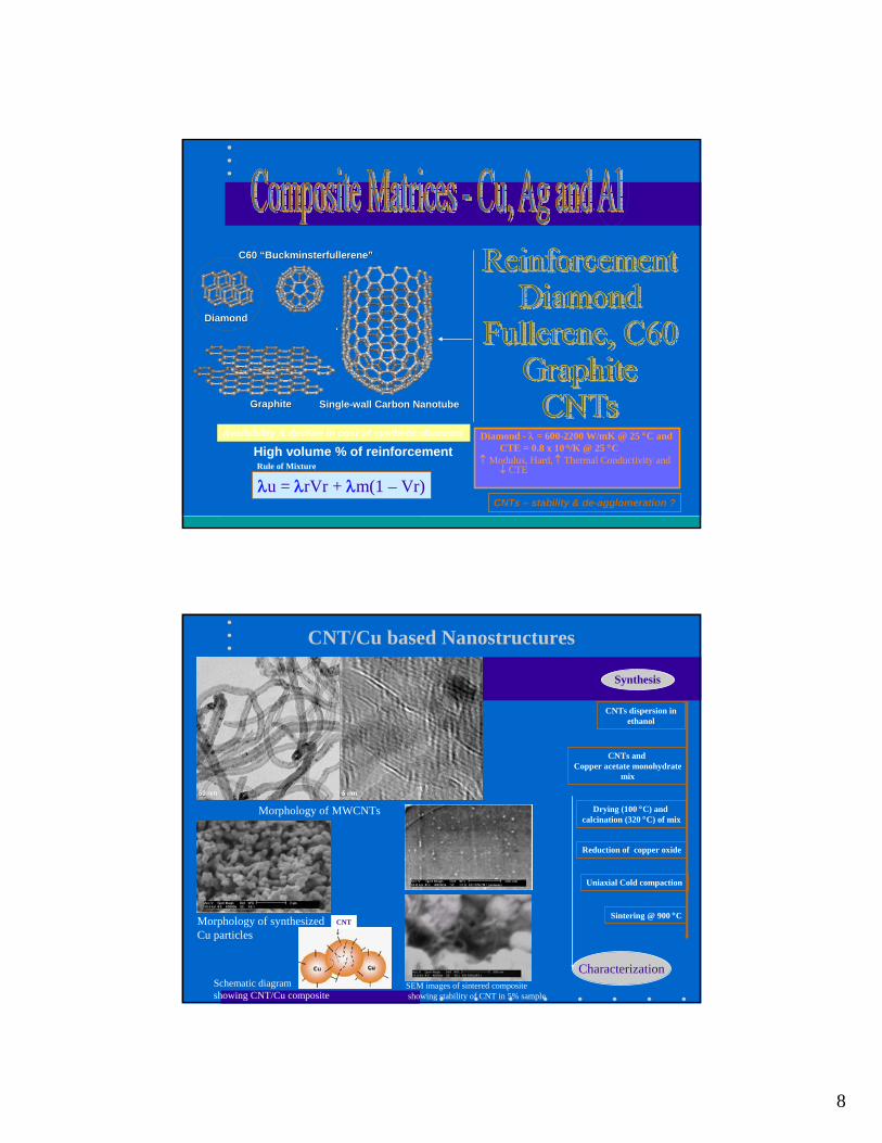
Diamond - λ = 600-2200 W/mK @ 25 °C andCTE = 0.8 x 10⁻⁶/K @ 25 °C
↑ Modulus, Hard, ↑ Thermal Conductivity and ↓ CTE
λu = λrVr + λm(1 – Vr)Rule of MixtureHigh volume % of reinforcement
DiamondDiamond
C60 C60 ““BuckminsterfullereneBuckminsterfullerene””
GraphiteGraphite SingleSingle--wall Carbon Nanotubewall Carbon Nanotube
CNTs – stability & de-agglomeration ?
Availability & decline in cost of synthetic diamond
CNT/Cu based Nanostructures
Morphology of MWCNTs
Morphology of synthesized Cu particles
SEM images of sintered compositeshowing stability of CNT in 5% sample
CNTs and Copper acetate monohydrate
mix
CNTs dispersion in ethanol
Drying (100 °C) and calcination (320 °C) of mix
Reduction of copper oxide
Uniaxial Cold compaction
Sintering @ 900 °C
Characterization
Synthesis
Schematic diagram showing CNT/Cu composite
CNT
9
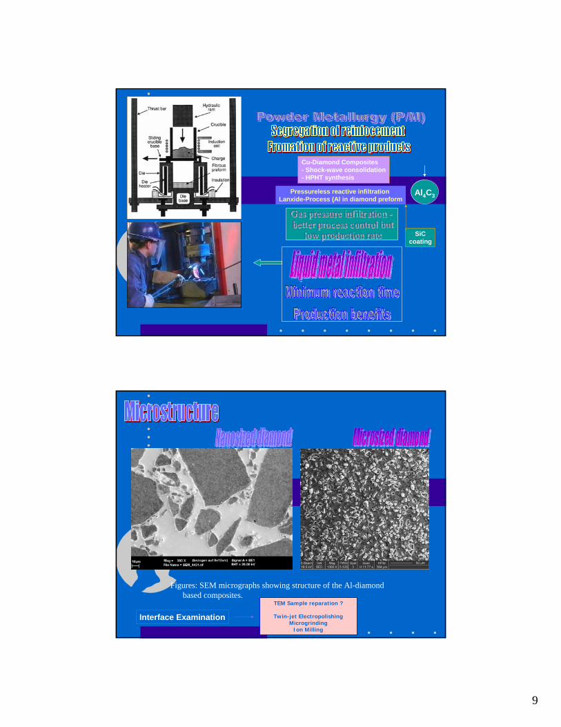
Al4C3Pressureless reactive infiltration
Lanxide-Process (Al in diamond preform
SiCcoating
Cu-Diamond Composites- Shock-wave consolidation- HPHT synthesis
Figures: SEM micrographs showing structure of the Al-diamond based composites.
TEM Sample reparation ?
Twin-jet ElectropolishingMicrogrinding
Ion Milling
Interface Examination
10
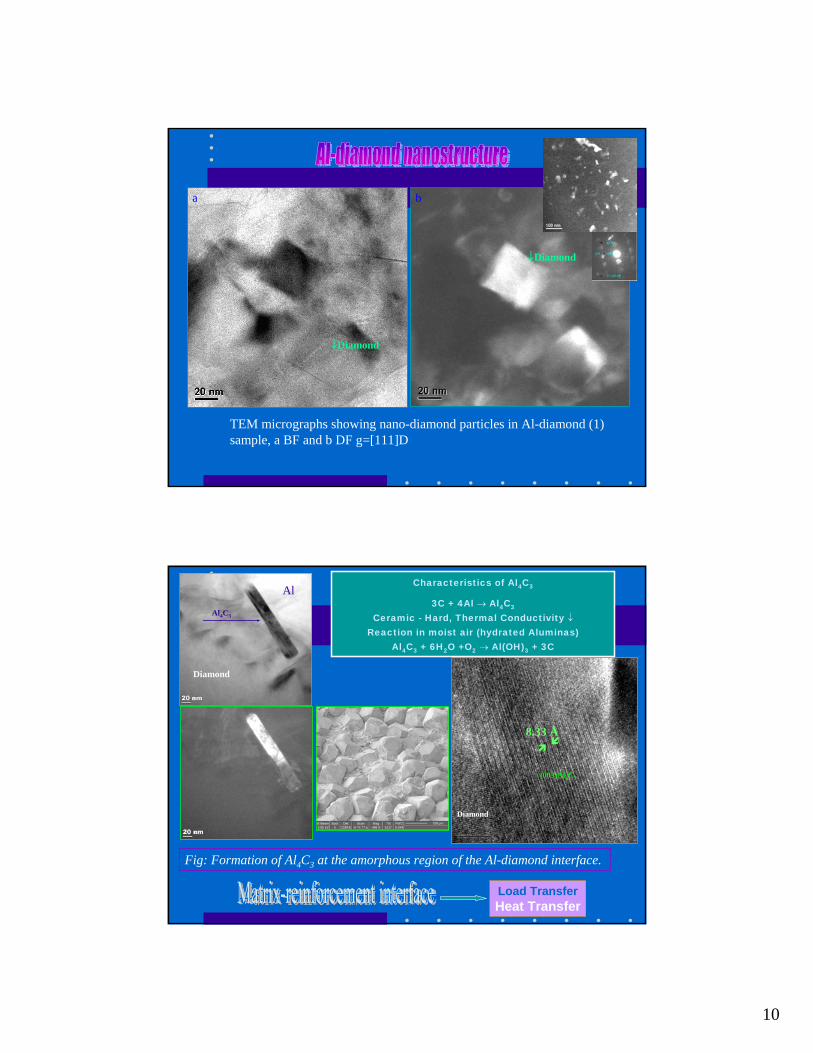
TEM micrographs showing nano-diamond particles in Al-diamond (1) sample, a BF and b DF g=[111]D
↓Diamond
↓Diamond
a b
Fig: Formation of Al4C3 at the amorphous region of the Al-diamond interface.
8.33 Å
Diamond
(003)Al4C3
Diamond
Al4C3
AlCharacteristics of Al4C3
3C + 4Al → Al4C3
Ceramic - Hard, Thermal Conductivity ↓Reaction in moist air (hydrated Aluminas)
Al4C3 + 6H2O +O2 → Al(OH)3 + 3C
Load TransferHeat Transfer
11
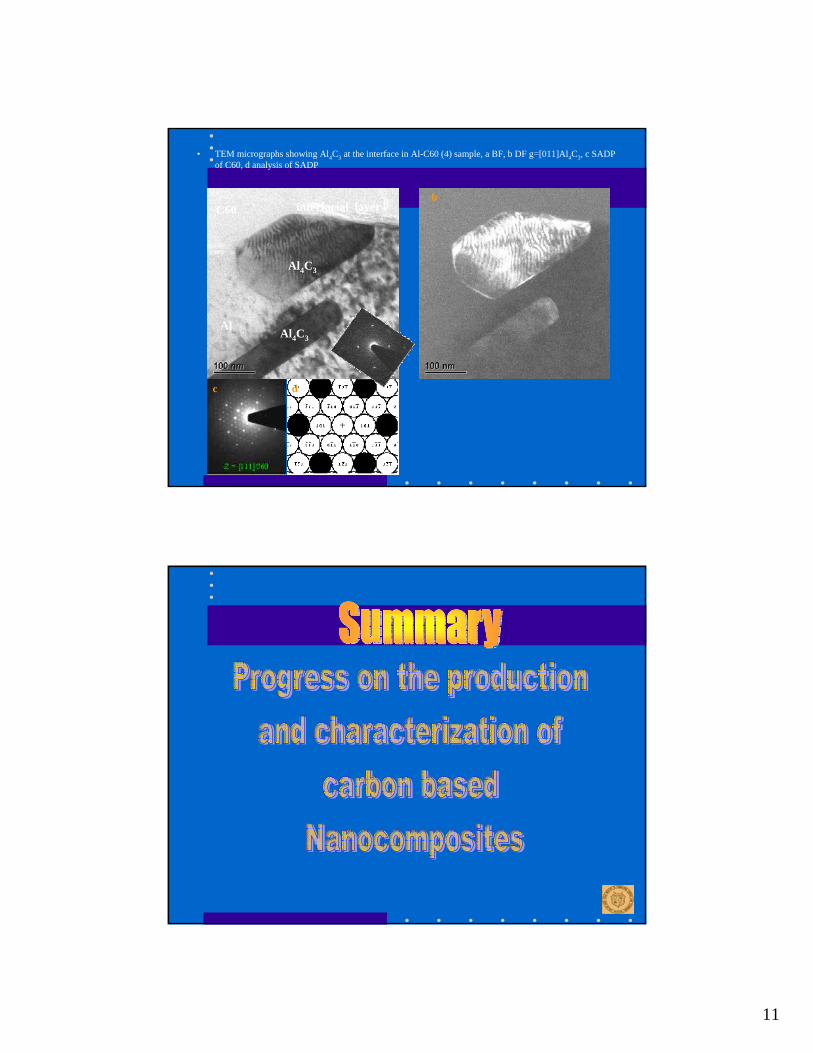
• TEM micrographs showing Al4C3 at the interface in Al-C60 (4) sample, a BF, b DF g=[011]Al4C3, c SADP of C60, d analysis of SADP
dc
binterfacial layer↓
AlAl4C3
Al4C3
C60

12