Fourier Transforms in Radar and Signal Processing - DSP-Book

FAST FOURIER TRANSFORMS ON ADISTRIBUTED DIGITAL SIGNAL PROCESSOR
By
OMAR SATTARIB.S. (University of California, Davis) June, 2002
THESIS
Submitted in partial satisfaction of the requirements for the degree of
MASTER OF SCIENCE
in
Electrical and Computer Engineering
in the
OFFICE OF GRADUATE STUDIES
of the
UNIVERSITY OF CALIFORNIA
DAVIS
Approved:
Chair, Dr. Bevan M. Baas
Member, Dr. Venkatesh Akella
Member, Dr. Hussain Al-Asaad
Committee in charge2004
– i –

c© Copyright by Omar Sattari 2004All Rights Reserved

Abstract
Fast Fourier Transforms are used in a variety of Digital Signal Processing
applications. As semiconductor process technology becomes more refined, the ability
to implement faster and more efficient FFTs increases. However, due to the high
costs and design time of custom FFT processors, implementation of the FFT on pro-
grammable or reconfigurable platforms is practical. In this work, we present mapping
of FFTs of various lengths to a programmable, reconfigurable array of processors.
The design of hardware address generators is also presented, as it is tightly cou-
pled with implementation of the Fast Fourier Transform. The reconfigurable array of
processors is named Asynchronous Array of Simple Processors (AsAP). A Register
Transfer Level (RTL) model of the AsAP architecture is used to simulate Fast Fourier
Transforms. Coding for the FFTs is done primarily with assembly-level code. Three
FFTs of length 32, 64, and 1024 points were mapped and simulated onto AsAP. The
accuracy of each FFT was verified by comparing simulation results to an independent
model.
– iii –

Acknowledgments
I would like to thank my advisor, Professor Bevan Baas. In addition to guiding
me through this research, he has taught me lessons which I know have made me a better
engineer. His willingness to spend time with me is sincerely appreciated.
I thank Professor Venkatesh Akella and Professor Hussain Al-Asaad for their valu-
able insight and their consultation. Their different perspectives helped me produce a better
thesis.
The University of California, Davis has provided a stable, enriching environment
for me to study in, and I am grateful for that. I would like to thank Alza Corporation for
providing me with a scholarship that has helped me make this journey. Intel corporation
has donated computing equipment which accelerated research in the VCL lab; thank you.
To Mike Lai, Mike Meeuwsen, Ryan Apperson, and Zhiyi Yu, I have thoroughly
enjoyed the time we spent together in the VCL lab. Interaction with you has helped advance
my research. Thank you for the discussions, the debates, the comedy, and the respect.
My father Saied and my mother Najla have made education the top priority
throughout my life. They have provided a warm and loving home, in addition to sup-
porting my education and my interests. There is no way I can reciprocate the twenty four
years of sacrifice you have made for me and my siblings. I can only thank you.
To my sister Nazaneen, and my brother Haroon, thanks for encouraging me and
showing me how much you love me. I am faithfully waiting for the days that I can celebrate
your great accomplishments with you.
– iv –

Contents
Abstract iii
Acknowledgments iv
List of Figures vii
List of Tables viii
1 Introduction 1
1.1 Project Goals . . . . . . . . . . . . . . . . . . . . . . . . . . . . . . . . . . . 11.2 Overview . . . . . . . . . . . . . . . . . . . . . . . . . . . . . . . . . . . . . 1
2 Discrete and Fast Fourier Transforms 3
2.1 The Continuous Fourier Transform . . . . . . . . . . . . . . . . . . . . . . . 32.2 The Discrete Fourier Transform . . . . . . . . . . . . . . . . . . . . . . . . . 42.3 The Fast Fourier Transform . . . . . . . . . . . . . . . . . . . . . . . . . . . 5
3 FFT Implementation 7
3.1 Butterflies . . . . . . . . . . . . . . . . . . . . . . . . . . . . . . . . . . . . . 83.2 Memory Requirements . . . . . . . . . . . . . . . . . . . . . . . . . . . . . . 83.3 Memory Access Patterns . . . . . . . . . . . . . . . . . . . . . . . . . . . . . 93.4 Bit Reversal . . . . . . . . . . . . . . . . . . . . . . . . . . . . . . . . . . . . 113.5 Related Work . . . . . . . . . . . . . . . . . . . . . . . . . . . . . . . . . . . 12
4 The AsAP DSP 14
4.1 Array Topology . . . . . . . . . . . . . . . . . . . . . . . . . . . . . . . . . . 164.2 Instruction Set . . . . . . . . . . . . . . . . . . . . . . . . . . . . . . . . . . 174.3 Memories . . . . . . . . . . . . . . . . . . . . . . . . . . . . . . . . . . . . . 174.4 FIFOs . . . . . . . . . . . . . . . . . . . . . . . . . . . . . . . . . . . . . . . 194.5 Datapath and Pipeline . . . . . . . . . . . . . . . . . . . . . . . . . . . . . . 194.6 Configuration . . . . . . . . . . . . . . . . . . . . . . . . . . . . . . . . . . . 204.7 Local Clock Generators . . . . . . . . . . . . . . . . . . . . . . . . . . . . . 21
5 Address Generation Hardware 23
5.1 Address Generator Interface . . . . . . . . . . . . . . . . . . . . . . . . . . . 235.2 Address Generator Design . . . . . . . . . . . . . . . . . . . . . . . . . . . . 25
– v –
6 Mapping FFTs on to AsAP 28
6.1 Using Address Pointers and Address Generators . . . . . . . . . . . . . . . 286.1.1 Address Pointers . . . . . . . . . . . . . . . . . . . . . . . . . . . . . 296.1.2 Address Generators . . . . . . . . . . . . . . . . . . . . . . . . . . . 30
6.2 Butterflies . . . . . . . . . . . . . . . . . . . . . . . . . . . . . . . . . . . . . 316.3 Bit-Reversal . . . . . . . . . . . . . . . . . . . . . . . . . . . . . . . . . . . . 366.4 Memory Addressing . . . . . . . . . . . . . . . . . . . . . . . . . . . . . . . 366.5 Long FFTs . . . . . . . . . . . . . . . . . . . . . . . . . . . . . . . . . . . . 38
6.5.1 The Cached FFT Algorithm . . . . . . . . . . . . . . . . . . . . . . . 396.5.2 Large Memories . . . . . . . . . . . . . . . . . . . . . . . . . . . . . . 41
7 FFTs implemented on AsAP 43
7.1 32-Point FFT . . . . . . . . . . . . . . . . . . . . . . . . . . . . . . . . . . . 447.1.1 Bit Reverse Processor . . . . . . . . . . . . . . . . . . . . . . . . . . 447.1.2 Butterfly Processor . . . . . . . . . . . . . . . . . . . . . . . . . . . . 45
7.2 64-Point FFT . . . . . . . . . . . . . . . . . . . . . . . . . . . . . . . . . . . 487.2.1 Memory Processor . . . . . . . . . . . . . . . . . . . . . . . . . . . . 507.2.2 Butterfly Processor . . . . . . . . . . . . . . . . . . . . . . . . . . . . 527.2.3 Shuffle Processor . . . . . . . . . . . . . . . . . . . . . . . . . . . . . 547.2.4 Eight Processor Version . . . . . . . . . . . . . . . . . . . . . . . . . 55
7.3 1024-Point FFT . . . . . . . . . . . . . . . . . . . . . . . . . . . . . . . . . . 567.3.1 Bit Reverse Processor . . . . . . . . . . . . . . . . . . . . . . . . . . 577.3.2 First-Epoch Shuffle Processor . . . . . . . . . . . . . . . . . . . . . . 617.3.3 Second-Epoch Twiddle Factor Generator Processor . . . . . . . . . . 63
8 Conclusion 69
8.1 Contributions . . . . . . . . . . . . . . . . . . . . . . . . . . . . . . . . . . . 698.2 Future Work . . . . . . . . . . . . . . . . . . . . . . . . . . . . . . . . . . . 69
8.2.1 Assembly Code for a Pipelined AsAP Architecture . . . . . . . . . . 698.2.2 Performance Optimizations . . . . . . . . . . . . . . . . . . . . . . . 70
Bibliography 71
– vi –
List of Figures
2.1 A radix-2 FFT butterfly . . . . . . . . . . . . . . . . . . . . . . . . . . . . . 52.2 An 8-point DFT decomposed to two 4-point DFTs . . . . . . . . . . . . . . 52.3 An 8-point FFT . . . . . . . . . . . . . . . . . . . . . . . . . . . . . . . . . 6
3.1 Bit Reversed Addresses . . . . . . . . . . . . . . . . . . . . . . . . . . . . . 11
4.1 A block diagram for a single AsAP processor . . . . . . . . . . . . . . . . . 154.2 Dataflow for a fine-granularity 8-tap FIR filter . . . . . . . . . . . . . . . . 164.3 Sample configuration code for an application . . . . . . . . . . . . . . . . . 214.4 Sample assembly code to load constants for an application . . . . . . . . . . 214.5 Sample assembly code for an application . . . . . . . . . . . . . . . . . . . . 224.6 An overview of configuration and testing . . . . . . . . . . . . . . . . . . . . 22
5.1 Data Address Generator . . . . . . . . . . . . . . . . . . . . . . . . . . . . . 255.2 Example of Split-Mask-Lo Operation . . . . . . . . . . . . . . . . . . . . . . 26
6.1 Dynamic Configuration Memory Map . . . . . . . . . . . . . . . . . . . . . 296.2 A 16-bit multiplication . . . . . . . . . . . . . . . . . . . . . . . . . . . . . . 336.3 A special fixed-point multiply . . . . . . . . . . . . . . . . . . . . . . . . . . 336.4 FFT Butterfly Error . . . . . . . . . . . . . . . . . . . . . . . . . . . . . . . 346.5 A 64-point Cached-FFT dataflow diagram . . . . . . . . . . . . . . . . . . . 40
7.1 Dataflow diagram for a two-processor 32-point complex FFT . . . . . . . . 447.2 32-Point FFT Accuracy . . . . . . . . . . . . . . . . . . . . . . . . . . . . . 497.3 Dataflow diagram for a 4-processor 64-point complex FFT . . . . . . . . . . 507.4 64-Point FFT Accuracy . . . . . . . . . . . . . . . . . . . . . . . . . . . . . 557.5 Dataflow diagram for an eight-processor 64-point complex FFT . . . . . . . 567.6 Dataflow diagram for a 6-processor 1024-point complex FFT . . . . . . . . 577.7 1024-Point FFT Accuracy . . . . . . . . . . . . . . . . . . . . . . . . . . . . 667.8 Dataflow diagram for a 25-processor 1024-point complex FFT . . . . . . . . 68
– vii –
List of Tables
3.1 8-Point FFT data addresses . . . . . . . . . . . . . . . . . . . . . . . . . . . 103.2 8-Point FFT twiddle addresses . . . . . . . . . . . . . . . . . . . . . . . . . 103.3 Addresses for a 64-point FFT . . . . . . . . . . . . . . . . . . . . . . . . . . 103.4 Real and Imaginary addresses for a 64-point FFT . . . . . . . . . . . . . . . 113.5 FFTs Implemented on Processors . . . . . . . . . . . . . . . . . . . . . . . . 13
4.1 Instruction Formats . . . . . . . . . . . . . . . . . . . . . . . . . . . . . . . 18
5.1 Address Generator Inputs . . . . . . . . . . . . . . . . . . . . . . . . . . . . 24
6.1 Real and Imaginary addresses for a 64-point Cached FFT . . . . . . . . . . 41
7.1 Real and Imaginary addresses for a two-epoch 1024-point Cached FFT . . . 587.2 Real and Imaginary addresses for memory shuffle in a 1024-point Cached FFT 587.3 Processor Utilization for FFT Applications . . . . . . . . . . . . . . . . . . 67
– viii –

1
Chapter 1
Introduction
The Fast Fourier Transform (FFT) is an essential algorithm in digital signal pro-
cessing. It is employed in various applications such as radar, wireless communication,
medical imaging, spectral analysis, and acoustics. Fast Fourier Transforms have been imple-
mented on different platforms, ranging from general purpose processors to specially designed
computer chips. Recent increases in microchip fabrication costs have made it more difficult
to produce custom designs for applications. Implementation of digital signal processing
algorithms, such as the FFT, on high-performance reconfigurable systems is becoming in-
creasingly attractive.
1.1 Project Goals
The goal of this project is to implement Fast Fourier Transforms on a parallel, re-
configurable processor array. Also, compromises between processor area and computational
throughput will be explored.
1.2 Overview
Chapter 2 introduces the Discrete Fourier Transform and the radix-2 Decimation
in Time Fast Fourier Transform. In Chapter 3, FFT implementation techniques are dis-
cussed, as well as related work on the topic of FFT implementation. Chapter 4 presents the

CHAPTER 1. INTRODUCTION 2
AsAP architecture, which FFTs will be mapped onto. Chapter 5 introduces the address
generators that were designed for AsAP as part of this work. Chapter 6 is a discussion
on how to map algorithms specifically to the AsAP DSP, and includes an introduction to
the Cached FFT Algorithm. Chapter 7 presents each of the FFTs implemented on AsAP,
including assembly source code.
3
Chapter 2
Discrete and Fast Fourier
Transforms
This chapter presents the Continuous Fourier transform, the Discrete Fourier
Transform, and the Fast Fourier Transform. This presentation, which assumes background
knowledge in signal processing, is brief. For a more in-depth analysis and history of these
topics, several introductory textbooks [1, 2] can be consulted.
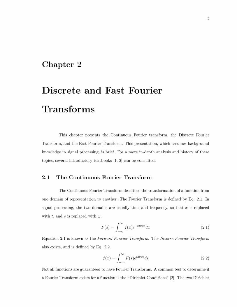
2.1 The Continuous Fourier Transform
The Continuous Fourier Transform describes the transformation of a function from
one domain of representation to another. The Fourier Transform is defined by Eq. 2.1. In
signal processing, the two domains are usually time and frequency, so that x is replaced
with t, and s is replaced with ω.
F (s) =
∫∞
−∞
f(x)e−i2πxsdx (2.1)
Equation 2.1 is known as the Forward Fourier Transform. The Inverse Fourier Transform
also exists, and is defined by Eq. 2.2.
f(x) =
∫∞
−∞
F (s)ei2πxsds (2.2)
Not all functions are guaranteed to have Fourier Transforms. A common test to determine if
a Fourier Transform exists for a function is the “Dirichlet Conditions” [2]. The two Dirichlet
CHAPTER 2. DISCRETE AND FAST FOURIER TRANSFORMS 4
Conditions for the existence of a Fourier Transform are that the function has a finite integral
over its entire domain, and that the function is continuous or has only finite discontinuities.
Although these conditions guarantee the existence of the Fourier Transform for a function,
there are functions that do not meet the conditions but still have Fourier Transforms. For
this reason, the Dirichlet Conditions are sufficient but not necessary conditions to prove the
existence of a Fourier Transform.
2.2 The Discrete Fourier Transform
The Discrete Fourier Transform converts discrete data from one domain to another.
The data (a series of points) must have finite length, and usually represents the periodic
sampling of a continuous signal. Equation 2.3 describes X(k), the DFT of an N -point input
sequence x(n). X(k), which also is of length N, is the frequency domain representation of
x(n).
X(k) =N−1∑n=0
x(n)e−i2πnk/N , k = 0, 1, ..., N − 1 (2.3)
A different (shorter) way to define the DFT is Eq. 2.4.
X(k) =
N−1∑n=0
x(n)W nkN , k = 0, 1, ..., N − 1 (2.4)
In this context, WN is known as the twiddle factor and is defined by,
WN = e−i2π/N . (2.5)
Using the twiddle factor, the definition of the inverse DFT is,
x(n) =1
N
N−1∑n=0
X(k)W−nkN , n = 0, 1, ..., N − 1 . (2.6)
The DFT is better-suited for implementation on computers than the continuous Fourier
Transform. Computers can store only a finite set of data in memory, and have no way to
fully represent a continuous signal using individual points. DFTs are transforms of finite-
length sequences, which can be represented in computers (notwithstanding quantization
error of individual points). Implementing the DFT or inverse DFT on a computer will
require 2N memory locations in addition to the memory space required to (if necessary)

CHAPTER 2. DISCRETE AND FAST FOURIER TRANSFORMS 5
Bm
Am
Am
AmBm+1
Am+1
WNr
WNr
Bm
WNr
Bm
Am+1
Bm+1
+
−=
=
Figure 2.1: A radix-2 FFT butterfly
W80
x[0]
x[2]
x[4]
x[6]
x[1]
x[5]
x[7]
x[3]
X[0]
X[1]
X[3]
X[2]
X[4]
X[5]
X[6]
X[7]
W8
W8
W8
1
2
3
X[4]
X[5]
X[6]
X[7]
X[0]x[0]
x[1]
x[2]
x[3]
x[4]
x[5]
x[6]
x[7]
X[1]
X[2]
X[3]
8 Point DFT
4 Point DFT
4 Point DFT
Figure 2.2: An 8-point DFT decomposed to two 4-point DFTs
store all of the twiddle factors as constants. A sum of 2N memory locations are required
because N memory locations are occupied by x(n), and the other N are occupied by the
result, X(k). Approximately N 2 complex multiplications and N(N − 1) complex additions
are required to complete a DFT or inverse DFT of an input sequence of length N .
2.3 The Fast Fourier Transform
Fast Fourier Transform is a group of algorithms that are more computationally
efficient than the standard DFT. Cooley and Tukey are noted most often for presenting the
algorithm in a research paper [3] for the journal “Mathematics of Computation.” We discuss

CHAPTER 2. DISCRETE AND FAST FOURIER TRANSFORMS 6
W80
W80
W80
W80
W80
W80
W81
W82
W83
W80
W82
W82
X[0]
X[1]
X[3]
X[2]
X[4]
X[5]
X[6]
X[7]
x[0]
x[4]
x[2]
x[6]
x[1]
x[5]
x[3]
x[7]
Figure 2.3: An 8-point FFT
the key points of FFTs instead of presenting a derivation of the entire class of algorithms.
There are textbooks that present the derivation, along with a thorough discussion of FFT
algorithms [1, 2]. The FFTs discussed in this work are Decimation-In-Time (DIT), radix-2
FFTs. Decimation-In-Time FFTs focus on reorganizing the input sequence x[n] to reduce
computation. The length of the input sequence is always a power of two in radix-2 FFTs.
The DIT FFT is more efficient than the DFT because the FFT is a recursive
decomposition of the DFT into smaller and smaller DFTs. The smallest useful DFT is a
radix-2 butterfly. Figure 2.1 describes a radix-2 butterfly. An FFT of length N can be
reduced to two separate FFTs of length N/2, followed by N/2 butterflies. Figure 2.2 is a
data flow diagram that shows how an 8-point DFT can be reduced in such a manner. The
decomposition can be continued until only radix-2 butterflies remain, as in Fig. 2.3. This
figure shows that there are 4 butterflies per stage in an 8-point FFT. Each butterfly requires
a complex multiplication and two complex additions (one add, one subtract). There are
log2(N) stages for an N -point FFT. Therefore, there are N/2 log2(N) complex multiplies per
FFT, and N log2(N) complex additions per FFT. A standard DFT requires N 2 operations
because for each output point in X[k] the entire input sequence x[n] is multiplied by a
twiddle factor. For long FFTs, N log2(N) operations are orders of magnitude fewer than
N2.
7
Chapter 3
FFT Implementation
Implementation of DIT FFTs on digital computers can be done in various ways
depending on the computer hardware available. Memory space and processor capabilities
are two factors to consider for implementation. Processors that have floating point hardware
can provide very accurate results, but are complex. Processors that don’t have floating point
hardware are usually limited to simpler implementations of the FFT, such as fixed-point
or block floating point. We focus on fixed-point implementations of the FFT, which have
more error than floating-point, but use only integer arithmetic.
First, we will briefly investigate the memory access patterns in the FFT, to give
insight on how to map the algorithm. Figure 2.3 shows that the indices of the output X[k]
are in consecutive order, but the input x[k] is not, and has a complicated pattern. With a
similar dataflow, it is possible to switch the order of input and output, so that the input
is consecutive and the output is irregular. In order to have both the input and output
in consecutive order, the dataflow needs to be changed significantly, and the pattern of
data access becomes extremely complicated. Instead of changing the dataflow inside of the
FFT, it’s easier to simply presort the input data to match the complex pattern, before
computation of the FFT.

CHAPTER 3. FFT IMPLEMENTATION 8
3.1 Butterflies
Each point in x[k] has a real component and an imaginary component. As a result,
a complex multiplication requires four integer multiplies and two integer additions. The
following equation is an example of an expanded complex multiplication, where j =√−1 .
(a + bj)(c + dj) = (ac − bd) + j(ad + bc) (3.1)
For a butterfly, there are two complex additions one complex multiplication. This brings
the total number of integer computations to four multiplies and four adds.
3.2 Memory Requirements
Since the FFT breaks the Fourier Transform (conveniently) into stages, it is nec-
essary to have only one array that can hold all N points. Once a stage is complete, the
only consumer of its data is the next stage, so the same array of points can be used over
and over as a conduit between stages. Still, when implementing the FFT on a computer,
it is advantageous to have more memory than the number of inputs N . If there is enough
memory to accommodate all N inputs and all N/2 twiddle factors, most FFT algorithms
allow all butterflies to be executed “in-place.” This means that for each butterfly, the inputs
are loaded from the appropriate locations, the butterfly is computed, and the results are
stored back to the original locations. As a result of using this method, all the butterflies
in a single stage should be executed and their results stored before moving on to the next
stage. However, in a single stage, the butterflies need not be executed in any particular
order, because no two butterflies share the same input or output.
Each point in an FFT has a real component and an imaginary component. Con-
sidering the example of a 16-bit complex point, the point can be stored as a single 32-bit
word, or as two separate 16-bit words. We consider the case where a point is stored as two
memory words. For an 8-point FFT, 16 words of memory are therefore necessary. Also,
there are four unique twiddle factors, so an additional eight words of memory are required,
unless the twiddle factors are supplied by an outside source. It is also possible to compute
twiddle factors as they become necessary, however this may reduce the effective throughput
CHAPTER 3. FFT IMPLEMENTATION 9
of the FFT if there is only one computation engine and FFTs are being executed repeatedly.
There is a trade-off here, between memory space and computation time. We assume that
all twiddle factors are stored in memory. In this case, an N -point FFT requires 2N memory
words to store data, and N words to store twiddle factors, for a total of 3N memory words.
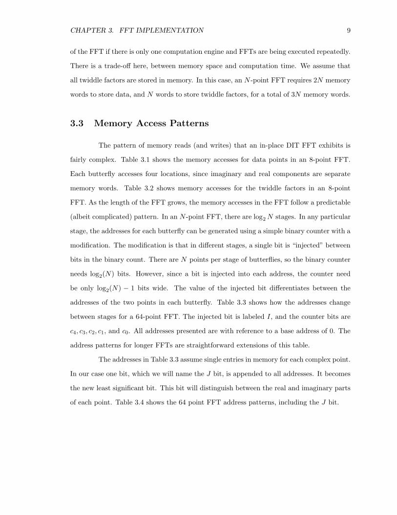
3.3 Memory Access Patterns
The pattern of memory reads (and writes) that an in-place DIT FFT exhibits is
fairly complex. Table 3.1 shows the memory accesses for data points in an 8-point FFT.
Each butterfly accesses four locations, since imaginary and real components are separate
memory words. Table 3.2 shows memory accesses for the twiddle factors in an 8-point
FFT. As the length of the FFT grows, the memory accesses in the FFT follow a predictable
(albeit complicated) pattern. In an N -point FFT, there are log2 N stages. In any particular
stage, the addresses for each butterfly can be generated using a simple binary counter with a
modification. The modification is that in different stages, a single bit is “injected” between
bits in the binary count. There are N points per stage of butterflies, so the binary counter
needs log2(N) bits. However, since a bit is injected into each address, the counter need
be only log2(N) − 1 bits wide. The value of the injected bit differentiates between the
addresses of the two points in each butterfly. Table 3.3 shows how the addresses change
between stages for a 64-point FFT. The injected bit is labeled I, and the counter bits are
c4, c3, c2, c1, and c0. All addresses presented are with reference to a base address of 0. The
address patterns for longer FFTs are straightforward extensions of this table.
The addresses in Table 3.3 assume single entries in memory for each complex point.
In our case one bit, which we will name the J bit, is appended to all addresses. It becomes
the new least significant bit. This bit will distinguish between the real and imaginary parts
of each point. Table 3.4 shows the 64 point FFT address patterns, including the J bit.

CHAPTER 3. FFT IMPLEMENTATION 10
Stage 0 Stage 1 Stage 2
Butterfly 0 addresses (point A) 0,1 0,1 0,1
Butterfly 0 addresses (point B) 2,3 4,5 8,9
Butterfly 1 addresses (point A) 4,5 2,3 2,3
Butterfly 1 addresses (point B) 6,7 6,7 10,11
Butterfly 2 addresses (point A) 8,9 8,9 4,5
Butterfly 2 addresses (point B) 10,11 12,13 12,13
Butterfly 3 addresses (point A) 12,13 10,11 6,7
Butterfly 3 addresses (point B) 14,15 14,15 14,15
Table 3.1: 8-Point FFT data addresses. The addresses for real and imaginary componentsof each point are separated by commas.
Stage 0 Stage 1 Stage 2
Butterfly 0 twiddle addresses 0,1 0,1 0,1
Butterfly 1 twiddle addresses 0,1 4,5 2,3
Butterfly 2 twiddle addresses 0,1 0,1 4,5
Butterfly 3 twiddle addresses 0,1 4,5 6,7
Table 3.2: 8-Point FFT twiddle addresses. The addresses for real and imaginary componentsof each W k
N twiddle factor are separated by commas.
Stage Butterfly Address Bits WN Address Bits
stage 0 c4c3c2c1c0I W 0000064
stage 1 c4c3c2c1Ic0 W c00000
64
stage 2 c4c3c2Ic1c0 W c1c000064
stage 3 c4c3Ic2c1c0 W c2c1c000
64
stage 4 c4Ic3c2c1c0 W c3c2c1c00
64
stage 5 Ic4c3c2c1c0 W c4c3c2c1c064
Table 3.3: Addresses for a 64-point FFT [4]
CHAPTER 3. FFT IMPLEMENTATION 11
Stage Butterfly Address Bits WN Address Bits
stage 0 c4c3c2c1c0IJ W 00000J64
stage 1 c4c3c2c1Ic0J W c00000J64
stage 2 c4c3c2Ic1c0J W c1c0000J64
stage 3 c4c3Ic2c1c0J W c2c1c000J64
stage 4 c4Ic3c2c1c0J W c3c2c1c00J64
stage 5 Ic4c3c2c1c0J W c4c3c2c1c0J64
Table 3.4: Real and Imaginary addresses for a 64-point FFT [4]
0
1
2
3
4
5
6
7
=
=
=
=
=
=
=
=
000
001
010
011
100
101
110
111
reversed −>
reversed −>
reversed −>
reversed −>
reversed −>
reversed −>
reversed −>
reversed −>
000
100
010
110
001
101
011
111
=
=
=
=
=
=
=
=
0
4
2
6
1
5
7
3
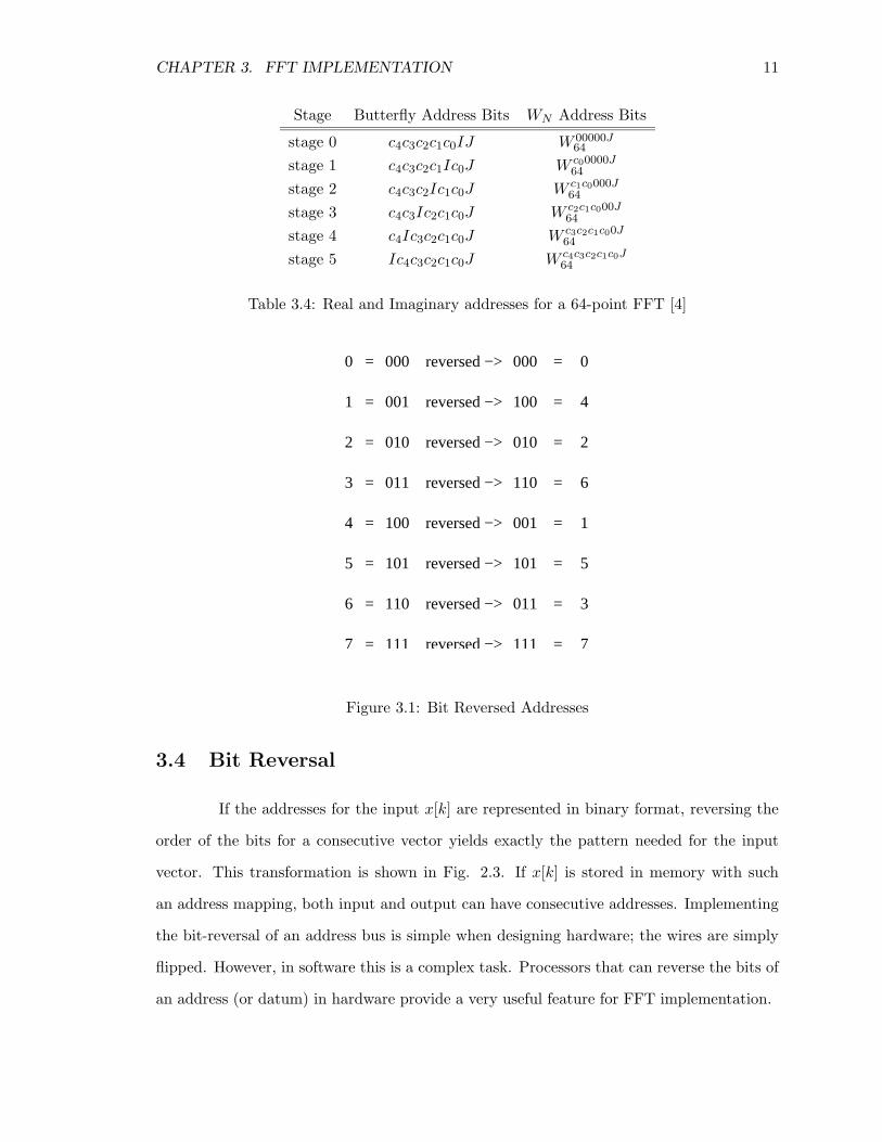
Figure 3.1: Bit Reversed Addresses
3.4 Bit Reversal
If the addresses for the input x[k] are represented in binary format, reversing the
order of the bits for a consecutive vector yields exactly the pattern needed for the input
vector. This transformation is shown in Fig. 2.3. If x[k] is stored in memory with such
an address mapping, both input and output can have consecutive addresses. Implementing
the bit-reversal of an address bus is simple when designing hardware; the wires are simply
flipped. However, in software this is a complex task. Processors that can reverse the bits of
an address (or datum) in hardware provide a very useful feature for FFT implementation.

CHAPTER 3. FFT IMPLEMENTATION 12
3.5 Related Work
Recent implementations of the FFT vary in terms of how much hardware and
software are used. At one end of the spectrum are chips designed to compute the FFT
exclusively. Examples of Application Specific Integrated Circuits (ASICs) for FFT are the
1024-point FFT processors designed and fabricated by He and Torkelson [5] or Baas [6].
In such designs, the application (FFT) is known before design, and the circuit is perfectly
matched to the workload.
Parallel architectures for computing the FFT have also been investigated. Shin,
Lee, and Lee have designed two-dimensional processor arrays for FFT computation [7, 8].
Yongjun Peng has designed an 8-processor parallel architecture for the computation of 256
through 4096-point FFTs [9]. Each of the processors computes an 8-point FFT using a
radix-8 butterfly, and a 1024-point FFT is expected to complete in 3.2 µsec.
Another paradigm for FFT implementation is an array of processors designed
for multimedia applications, not exclusively FFT. Such implementations usually involve
large amounts of software programming, but are very flexible in terms of applications that
can be programmed. Examples of such architectures are the MorphoSys Reconfigurable
Computation Platform [10], the Imagine Stream Processor [11], and VIRAM [12]. The
computation engine in the MorphoSys platform is an array of reconfigurable processing
cells. These cells communicate with each other using a data movement unit labeled “Frame
Buffer”. Various length FFTs were implemented on MorphoSys using radix-2 butterflies.
The Imagine processor is a single chip with 48 parallel Arithmetic Logic Units (ALUs). A
1024-point FFT was mapped to Imagine; the 10 stages of butterflies were separated into 10
kernels, and data are transferred between kernels. VIRAM has four 64-bit vector processors,
each with its own floating-point unit, in addition to 16 MB of DRAM. FFTs of length 128,
256, 512 and 1024 points were implemented on VIRAM [13].
Although AsAP is also an array of processors, it is designed with DSP applications
in mind, and has inherent properties that distinguish it from the mentioned designs. The
features of AsAP are discussed in the next chapter. Table 3.5 summarizes the capabilities
of various processors on which a 1024-point FFT has been implemented.

CH
AP
TE
R3.
FFT
IMP
LE
ME
NTAT
ION
13
Processor Type Year Technology Data Data Point 1024-point FFT
Width Format Execution Time
TM-66 Custom FFT - 0.8µm 32 bit float 65µsec
Spiffee1 Custom FFT 1995 0.7µm 20 bit fixed 30µsec
DSP-24 Custom FFT 1997 0.5µm 24 bit block float 21µsec
DoubleBW Custom FFT 2000 0.35µm 24 bit float 10µsec
ADSP 21061 Programmable DSP - - - float 460µsec
VIRAM Programmable 1999 - 16-64 bit float 37µsec*
Imagine Programmable 2002 0.15µm - - 20.6µsec
Kuo, Wen, Wu Programmable FFT 2003 0.35µm 16 bit fixed 167µsec
Peng Programmable FFT 2003 0.18µm 20 bit - 3.2µsec*
AsAP Prog., Reconf. DSP 2004 0.13µm 16 bit fixed 101µsec*
AsAP Prog., Reconf. DSP 2004 0.13µm 16 bit fixed 30µsec**
Table 3.5: FFTs Implemented on Processors [14]. AsAP has an estimated 1Ghz maximum clock frequency. FFTs Implemented onProcessors. A “*” indicates that the results are from simulations. A “**” indicates a projection based on simulations.

14
Chapter 4
The AsAP DSP
The AsAP (Asynchronous Array of Simple Processors) [15] architecture is a par-
allel reconfigurable two-dimensional array of single-issue processors. Each processor has its
own clock generation unit and can be configured to operate at a frequency different from
its neighbors. Communication between neighbors is achieved by dual-clock FIFOs, since
neighbor processors may have drastically varying clock frequencies. The entire AsAP has
one or more 16-bit input ports and one or more 16-bit output ports. These ports are directly
tied to individual processors in the array. Processors are pipelined with 16-bit fixed-point
datapaths. Instructions for AsAP processors are 32-bits wide. Each AsAP processor has a
64-entry instruction memory and a 128-word data memory.
DSP algorithms are generally deterministic and don’t rely on input data to make
program flow decisions. For example, the number of iterations that a loop executes is usually
pre-determined. In the same way, memory accesses are often pre-determined. Hardware
designers can take advantage of such features when designing DSPs. To help with processing
tasks that have complex (but deterministic) memory access patterns, each processor has
four address generators that calculate addresses for data memory. Figure 4.1 is an overview
of the key components in each AsAP DSP.

CHAPTER 4. THE ASAP DSP 15
FIFO 0
FIFO 1
DAG 0
DAG 1
DAG 2
DAG 3
CPU
Output (N)
Output (S)
Output (E)
Output (W)
Config
DCMem
O−Port
Clk Gen
IMem DMem
Input 0
Input 1
Figure 4.1: A block diagram for a single AsAP processor. Blocks labeled “DAG” representdata address generators.

CHAPTER 4. THE ASAP DSP 16
*
*
*
* *
*
*
*
+
+
+ +
+
+
+
f
f
f f fff
f f
f
Input Output
Figure 4.2: Dataflow for a fine-granularity 8-tap FIR filter. Processors marked “*” executemultiplications. Processors marked “+” execute additions. Processors marked “f” forwarddata to other processors.
4.1 Array Topology
Each processor in the array has two input FIFOs and one output port. Each input
FIFO has 32 entries and can be connected to the output port of a neighbor processor. The
choices for neighbor processor are north, south, west and east. Figure 4.2 shows an example
interconnection network for an FIR filter. Since there are only two input FIFOs, there can
be no more than two arrows pointing into a single processor. However, one processor can be
the source of data for multiple processors. Since there is one output port, all the processors
would receive the same data. The array topology of AsAP is well-suited for applications that
are composed of a series of independent tasks. Each of these tasks can be assigned to one or
more processors. As each processor is working on its task, the data that it needs becomes
available at its input FIFO. Since data “flows” through the system, the dependence on a
large global memory is reduced. Furthermore, an array of small high-throughput processors
is more effective than single-datapath DSPs because multiple datapaths process different
parts of the algorithm at the same time.

CHAPTER 4. THE ASAP DSP 17
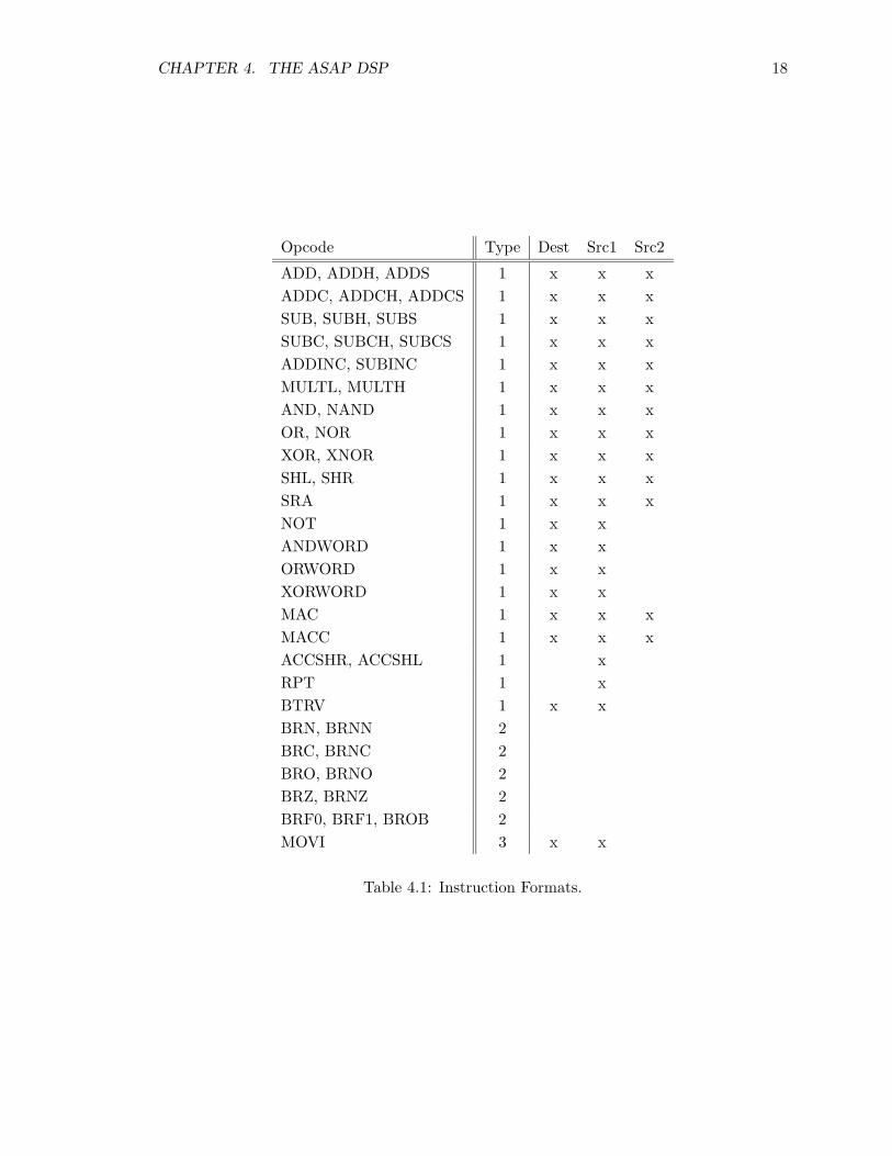
4.2 Instruction Set
In an effort to make the AsAP instruction set architecture as simple as possible,
the instruction format is fairly uniform. There is a 6-bit opcode field, an 8-bit destination
field, two 8-bit source fields, and a 2-bit NOP field. The NOP field allows each instruction
to specify up to 3 NOPs to execute after itself. These NOPs are used as a final resort if data
dependencies cannot be alleviated by scheduling or bypass paths. There are four condition
registers that specify whether the result of the instruction just executed is negative, has a
carry-out, has overflowed, or is zero. Not all instructions affect these registers. Condition
registers are used by branch instructions. AsAP instructions fall into 3 broad categories.
Instructions that typically load one or two sources and use some part of the ALU or mul-
tiply unit are denoted “Type 1” instructions. Branch instructions are denoted “Type 2”
instructions. The move immediate instruction is the only “Type 3” instruction. It is in a
separate category because it has a single 16-bit source. Table 4.1 lists all instructions and
their formats.
4.3 Memories
There are four memories in each AsAP processor. 1) The instruction memory
(IMem) is 32-bits wide, and has 64 entries. 2) The data memory (DMem) is 16-bits wide,
and has 128 entries. Although many algorithms may require more of both types of mem-
ory, we hope that such algorithms can be divided and spread across multiple processors.
The strategy in AsAP is to keep the size of each individual processor small so that more
processors can reside in a fixed area. Configuration memory (CMem) is also 8-bits wide,
and has only a handful of entries. 3) The configuration memory is composed of registers
(not RAM), and holds static settings like input FIFO connect directions and local clock
frequency. 4) The dynamic configuration memory (DCMem) is 16-bits wide and has 19
entries. DCMem is designed to hold configuration for parameters that can change during
runtime. It primarily holds the constants that govern the operation of the address gener-
ators, which can change at runtime. DCMem also holds 4 loadable address pointers and a
4-bit output port configuration. A processor can write to any combination of the 4 possible
CHAPTER 4. THE ASAP DSP 18
Opcode Type Dest Src1 Src2
ADD, ADDH, ADDS 1 x x x
ADDC, ADDCH, ADDCS 1 x x x
SUB, SUBH, SUBS 1 x x x
SUBC, SUBCH, SUBCS 1 x x x
ADDINC, SUBINC 1 x x x
MULTL, MULTH 1 x x x
AND, NAND 1 x x x
OR, NOR 1 x x x
XOR, XNOR 1 x x x
SHL, SHR 1 x x x
SRA 1 x x x
NOT 1 x x
ANDWORD 1 x x
ORWORD 1 x x
XORWORD 1 x x
MAC 1 x x x
MACC 1 x x x
ACCSHR, ACCSHL 1 x
RPT 1 x
BTRV 1 x x
BRN, BRNN 2
BRC, BRNC 2
BRO, BRNO 2
BRZ, BRNZ 2
BRF0, BRF1, BROB 2
MOVI 3 x x
Table 4.1: Instruction Formats.

CHAPTER 4. THE ASAP DSP 19
output directions, and this configuration can change at different points while the application
runs.
4.4 FIFOs
In AsAP, dual-clock FIFOs [16] are the core mechanism for communication between
neighbor processors. Each FIFO has a 32-word (16-bit) circular buffer to hold data in
transit. There are handshaking signals required between the FIFO and the entity that is
attempting to get data from, or send data to the FIFO. For example, the FIFO has an
output signal to let the sender know that there is no more space in the FIFO. Although all
32 words of the buffer may be occupied at some point, the FIFO will signal that the buffer
is full before all 32 words are occupied. This is because there is a latency between the time
that a FIFO signals full, and the time that the sender receives the signal and stops sending
data. During that time, the remaining few entries are being filled. The number of buffer
entries necessary to accommodate for latency is known as “reserve space.”
Each dual-clock FIFO has a read side and a write side. Data arrives into the write
side and is stored into the buffer. Data exits the FIFO on the read side. In AsAP processors,
FIFOs are used as input ports. Therefore, the read side is interfaced to the local processor,
and the write side is interfaced to an upstream processor. The upstream processor’s clock
signal is fed to the write side, along with other handshaking signals. The local processor’s
clock is fed to the read side, along with other handshaking signals. It is the responsibility of
the FIFO to make sure that data is correctly transferred between these two different clock
domains.
4.5 Datapath and Pipeline
AsAP processors have a 9-stage pipeline which was designed with a RISC-style
instruction set architecture in mind. At various locations in the pipeline, there are 16-bit
bypass registers which can be used explicitly in instructions as sources. These bypass
registers help alleviate the cycle penalties due to data dependence between instructions. In
CHAPTER 4. THE ASAP DSP 20
the AsAP pipeline, there is an instruction fetch stage, a decode stage, an operand fetch
stage, a source select stage, three execute stages, a result select stage, and a memory write-
back stage.
4.6 Configuration
Each AsAP processor has a hard-coded processor number. This processor number
is used to address the processor during configuration. Configuration (of IMem and CMem)
is done via a global configuration bus. Each processor is responsible for “listening” on the
configuration bus and determining if the data presented belongs to itself. If the data does
belong to a particular processor, that processor is responsible for storing the data in the
correct location. There is no handshaking on the configuration bus. The configuration bus
consists of an address bus and a data bus. The address bus has a group of bits dedicated
to selecting the processor, a groups of bits to select which memory is being written, and a
group of bits to address a location in that memory. Also, there is a broadcast bit in the
address bus, so that it is possible to configure all processors with the same value for some
memory location.
Applications that are mapped to AsAP and run on AsAP are referred to as “tests.”
For each test, there is a series of steps required to configure the AsAP chip and run the test.
The first step in the process is to stop all processors from executing any code and to load
CMem for each processor. The second step is to load and run (for each processor) programs
that load useful constants into DMem or DCMem. The third and final step is to load the
actual application program and allow it to run. For CMem, configuration parameters and
their values are specified for each processor in a configuration file. Figure 4.3 is an example
of a configuration file.
For DMem and DCMem, assembly code is assembled and loaded into IMem for
each processor. This assembly code is allowed to run, so that the constants are loaded into
DMem and DCMem. Figure 4.4 is an example of an assembly program that loads constants.
Finally, for IMem, the application assembly code is assembled and loaded into
IMem for each processor. Figure 4.5 is an example of an unscheduled assembly program for

CHAPTER 4. THE ASAP DSP 21
# ******* ********** ******************** **********************************# proc ** address ** value ************** comments *************************# ******* ********** ******************** **********************************
0,0 ibuf0 west # input processor 0,0 frequency d7 # frequency
Figure 4.3: Sample configuration code for an application
begin 0,0movi dcmem 18 1 // obuf = s,w,n,e (east)
done:
end
movi dmem 0 0 // dmem[0] = 0movi dmem 70 64 // dmem[70] = 64
br done // do nothing
Figure 4.4: Sample assembly code to load constants for an application
an application. An overall picture of the modules necessary for configuration and testing is
shown in Fig. 4.6.
4.7 Local Clock Generators
The local clock generator for each processor is digitally programmable. Normally,
it is programmed once during configuration, and retains that clock frequency until it is
re-configured. It is also “pausible,” so that if a processor is idle for a long period of time,
the clock no longer oscillates, which saves energy.

CHAPTER 4. THE ASAP DSP 22
begin 0,0
start:move dmem 70 #0 // data_ctr = 0
// ************** move data in ******************brloop:
or dcmem 5 dcmem 5 #1 // mask_and=127, mask_or=1
// ************** move data in ******************
// ************** move data out *****************move dcmem 0 #0 // aptr0 = 0outloop:move obuf aptr0 // obuf = dmem[aptr0]add dcmem 0 dcmem 0 #1 // aptr0 += 1sub null dcmem 0 dmem 71 // stop at 64
// ************** move data out *****************br startend
movi dcmem 5 32512 // mask_and=127, mask_or=0move ag0 ibuf0 // get data from ibuf0
move ag0pi ibuf0 // get data from ibuf0add dmem 70 dmem 70 #1 // data_ctr++sub null dmem 70 #32 // check if data_ctr = 32brnz brloop // branch back if not done
brnz outloop // branch back if not done
Figure 4.5: Sample assembly code for an application. This code moves data from an inputFIFO to DMem, then moves the data from DMem to OPort (obuf).
010101110010011011011011000101000101001010100101001000010001
010101110010011011011011000101000101001010100101001000010001
0101011100100110110110110001010001010010101001010010000100011011000101
0101011100100110110110110001010001010010101001010010000100011011000101
.
.
.
Proc 0,0 frequency d32Proc 0,0 ibuf1 westProc 0,0 ibuf0 north
Proc 1,0 ibuf0 east
Proc 0,0beginmove obuf ibuf0br 0end
beginproc 1,0
CONFIGURATION
ASSEMBLER
INSTRUCTION
ASSEMBLER
MULTIPROCESSORDSP CHIP
CONFIG
VERILOG VERILOGVERILOG
VERILOG
VERILOG
Top Level Testbench
ASSEMBLY CONFIGURATION
INPUTTEST
PATTERNS PATTERNSOUTPUT
READTESTWRITE
TEST
Figure 4.6: An overview of configuration and testing

23
Chapter 5
Address Generation Hardware
For algorithms with complex memory access patterns, address generators save
processor cycles by pre-computing addresses. An address generator in AsAP is essentially a
programmable pointer. Each processor has four address generators which can address any of
the 128 words in data memory. An address generator can be used as the destination, source1,
or source2 of an instruction word. When an instruction specifies an address generator as
one of its sources, DMem uses the address from the address generator to fetch data. In the
same manner, if the address generator is used as a destination, a write will occur to DMem,
with the target address specified by the address generator.
5.1 Address Generator Interface
Address generators can be used in two modes: normal and post-increment. In
normal mode, the address output of the address generator does not advance. In post-
increment mode, the address is advanced, but the new address is unavailable until the next
clock cycle. For normal mode, the assembly-code names for the address generators are ag0,
ag1, ag2, and ag3. The assembly-code names for post increment address generators are
ag0pi, ag1pi, ag2pi, and ag3pi. Even though there are 8 names, there are still only four
address generators.
Each address generator has a set of inputs that dictate its memory access pattern.
These inputs are: reset, enable, start addr, end addr, stride, direction, shr amt, bit rev, sml,
CHAPTER 5. ADDRESS GENERATION HARDWARE 24
Signal Word Width Function
(bits)
reset 1 load start addr into address generator
enable 1 allow add (or subtract) of stride to addr generator
start addr 7 start address
end addr 7 end address
stride 6 amount to increment or decrement address generator
direction 1 1=increment, 0=decrement
bit rev 1 reverse all 7 bits of address generator count register
shr amt 3 shift right bit-reversed address up to 7 places
sml 7 split-mask-lo, mask used to split address for fft
and mask 7 generic AND mask
or mask 7 generic OR mask
Table 5.1: Address Generator Inputs
and mask, and or mask. Since AsAP’s data memory has 128 words, addresses are seven bits
wide. As such, most of the masks are seven bits. Table 5.1 describes the size and function
of each address generator input.
Inside the address generator, there is a single seven-bit register that holds the
current address. This register is referred to as the count register. The most fundamental
decision made in the address generator is whether or not to advance the count register. The
count register can only be advanced when the address generator is in post-increment mode
(i.e. enable is asserted). If the direction input is asserted, then stride is added to the count
register. Conversely, if the direction input is held low, stride is subtracted from the count
register. The bit rev input is used to reverse the bits in the count register. The shr amt
input shifts the bit reversed address right up to seven bits. The bit rev and shr amt inputs
are commonly used to help generate addresses for FFT computation. Another input that
is used for FFT computation is sml (split-mask-lo). Split-mask-lo is intended to take on
the following values: “0000000”, “0000001”, “0000011”, “0000111”, “0001111”, “0011111”,
“0111111”, and “1111111.” Its functionality is discussed further in Section 5.2. The default
value for sml is “1111111,” so that its output is the unmodified count register. The last two
inputs used are and mask and or mask. The default value for and mask is “1111111,” so
CHAPTER 5. ADDRESS GENERATION HARDWARE 25
>> X
10
1 0
1
+ / −
0
count
(Bit−Reversal)
(SHL 1)
or_mask enablereset
end_addrshr_amt
bit_revand_mask stride
sml directionstart_addr
addr_out
Figure 5.1: Data Address Generator. Thin lines represent one-bit wires. Thick lines repre-sent seven-bit wires.
that it does not change the address. The default value for or mask is “0000000,” so that it
does not change the address. These two masks are useful for restricting addresses to certain
areas or blocks of the memory space.
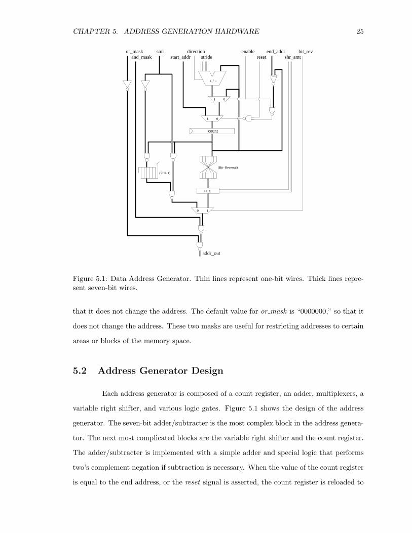
5.2 Address Generator Design
Each address generator is composed of a count register, an adder, multiplexers, a
variable right shifter, and various logic gates. Figure 5.1 shows the design of the address
generator. The seven-bit adder/subtracter is the most complex block in the address genera-
tor. The next most complicated blocks are the variable right shifter and the count register.
The adder/subtracter is implemented with a simple adder and special logic that performs
two’s complement negation if subtraction is necessary. When the value of the count register
is equal to the end address, or the reset signal is asserted, the count register is reloaded to

CHAPTER 5. ADDRESS GENERATION HARDWARE 26
start addr. This is implemented with a multiplexer and some logic (including XNOR gates
to compute equivalence).
Below the count register, there are essentially two choices for the output address
to take. Both are permutations of the count register. One of these choices is the bit-reverse
path. The seven bits of the count register are reversed, then shifted right by shr amt. The
variable shift amount allows bit reversal to be useful for FFTs of varying length (with an
upper limit of seven-bit addresses). The second choice for the output is the split-mask-lo
path. Addresses for points in the FFT have a single bit “injected” into the address at
different bit-positions (depending on the stage in the FFT). Split-mask-lo is a binary mask,
which in its simplest form is a string of 0’s followed by a string of ones. Figure 5.2 shows
how the split-mask-lo is applied to an input signal so that the result has an injected bit.
0 10 0 1 1 1XX X XX XX
XX 0 XX XX
original address:sml:
result address:
discarded bit:
injected bit:
Figure 5.2: Example of Split-Mask-Lo Operation
The new bit is added at the boundary between a string of zeros and a string of
ones in sml. The binary value of the inserted bit is zero. This can be changed further in
the address generator with or mask. The multiplexer that selects the signal from either
the bit-reverse path or the split-mask-lo path is controlled by a single bit input, bit rev.
If neither of these two permutations is needed, and just the count register is desired, then
bit rev should be set to 0 and sml should be set to “1111111.” The hardware is designed so
that the output is simply the count register when sml is “1111111.” The final modifications
that can be made to the address in the count register are the and mask and or mask. First,
the seven-bit and mask is applied to the signal from the multiplexer. This is normally used
to force some or all of the bits in the address to zeros. After that, the or mask is applied,
which allows any of the seven bits to be set to one.
The address generator is designed to reside in one to two pipeline stages in a
pipelined processor. The internal count register can be treated as one of the pipeline

CHAPTER 5. ADDRESS GENERATION HARDWARE 27
registers that separates stages. The logic above the count register is likely to be in the same
stage that instructions are decoded. The logic after the count register can be fed directly
into a memory, but this is unlikely because a memory will probably have more addressing
modes than just address generators. For this reason, the logic after the count register, in
combination with multiplexers that select the addressing mode, will be in another pipeline
stage. With these requirements taken into account, address generators were integrated into
AsAP.
28
Chapter 6
Mapping FFTs on to AsAP
Mapping algorithms to the AsAP DSP is a two-phase process. First, the program-
mer must decide how to partition the algorithm so that it can be distributed over multiple
processors in AsAP. This is assuming the algorithm is complex enough that it needs more
resources than one AsAP processor. Second, the programmer must write and test assembly
code for each active processor in the array, to implement the entire algorithm. How much
effort each of these phases receives has great impact on factors such as performance, power
consumption, energy usage and processor utilization. There are various trade-offs between
pairs or groups of these factors.
The first model of AsAP is implemented in Verilog HDL. This model is a single-
cycle behavioral model of the processor array, including FIFOs and configuration hardware.
Since the model does not describe the pipelined version of AsAP, hazards due to data
dependencies and structural conflicts are not apparent. The code presented does not include
any scheduling details.
6.1 Using Address Pointers and Address Generators
Address pointers and address generators provide the AsAP programmer with an
indirect way to access memory. They are pointers in the programming language sense of
the word; when de-referenced, they fetch data from data memory using the address they
currently hold. When an AsAP programmer wishes to de-reference an address pointer or

CHAPTER 6. MAPPING FFTS ON TO ASAP 29
address ptr 0
address ptr 2
BR DIR SHR_AMT
MASK_ORMASK_AND
SMLSTRIDE
START_ADDR END_ADDR
BR DIR SHR_AMT
START_ADDR
START_ADDR
START_ADDR
STRIDE
STRIDE
STRIDE
END_ADDR
END_ADDR
END_ADDR
SML
SML
SML
MASK_OR
MASK_OR
MASK_OR
BR
BR
DIR
DIR
SHR_AMT
SHR_AMT
MASK_AND
MASK_AND
MASK_AND
OBUF_CFG
ADDRESS
BIT
9
8
7
6
5
4
3
2
1
0
10
11
12
13
14
15
16
17
18
9 8 7 6 5 4 3 2 1 015 14 13 12 11 10
DAG0
DAG1
DAG2
DAG3
address ptr 1
address ptr 3
Figure 6.1: DCMem Map. Shaded addresses are not used. “BR”= bit-reverse, “DIR”=direction, “SML”= split-mask-lo, “SHR AMT”= shift right amount
address generator, the normal names are used (aptr0,aptr1,aptr2,aptr3,ag0,ag1,ag2,ag3).
When the programmer wants to change where the pointer is pointing to, changes must be
made to DCMem. Figure 6.1 shows all the fields in DCMem.
6.1.1 Address Pointers
Each AsAP processor has four address pointers in addition to its four address
generators. Address pointers are seven-bit registers that are mapped into DCMem. When
the field for an address pointer in DCMem is set to a particular value, the corresponding
address pointer can be used as a source or destination. The following lines of assembly code
are an example of how to use address pointers.
movi dcmem 0 15
move obuf aptr0
The first line loads DCMem[0] with “15,” so that aptr0 points to DMem[15]. The second
line uses aptr0 to access DMem (using the address 15) and moves the contents to the OPort
(also referred to as “obuf”). Since aptr0 and aptr1 are in the same memory word, writing

CHAPTER 6. MAPPING FFTS ON TO ASAP 30
a value to DCMem[0] overwrites the value for both pointers.
6.1.2 Address Generators
Configuring the address generators is similar to loading the address pointers. Mod-
ifying values in DCMem changes the behavior of the address generator. The following lines
of assembly code are an example of how to use address generators.
movi dcmem 2 32 // ag0 br=0, dir=1, shr_amt=0
movi dcmem 3 269 // ag0 start=1, end=13
movi dcmem 4 895 // ag0 stride=3, sml=1111111
movi dcmem 5 32512 // ag0 and_mask=1111111
// ag0 or_mask=0000000
rpt #10 // rpt next line 10 times
move obuf ag0pi // move to obuf DMem[ag0]
The first four lines move constants into DCMem to configure ag0. This address generator
is programmed to cycle through the following addresses: 1, 4, 7, 10, 13. After the address
generator reaches 13, the next address automatically returns to 1. This is because start addr
is set to 1 and end addr is set to 13. The repeat instruction causes the move instruction to
execute 10 times. The move instruction dereferences the address generator and moves the
data from DMem to the output port.
The programmer must make sure that the count register is the same as end addr
at some point in order to restart the sequence. If end addr and the count register never
match, the output will continue past 13. In the above case, the count register and the output
address are identical, but there are cases where they are not the same. An example of such
a case is if the and mask were set to “1111110.” The output sequence would then be: 0, 4,
6, 10, 12. The count register would still cycle through the original sequence (1, 4, 7, 10, 13).
If the programmer wants the address generator to restart at 0 after 12, then the end addr
should be set to 13, because that is the value in the count register that corresponds to the
end of the sequence.
It is possible to achieve the same results by simply using address pointers in a
controlled loop. This will be less code than the amount necessary to configure and use
address generators. However, using the address generators can speed up the execution of
code dramatically. Instead of wasting cycles incrementing the address pointer to calculate
CHAPTER 6. MAPPING FFTS ON TO ASAP 31
the next address and checking bounds, the move instruction can be executed repeatedly
with nearly no loop overhead. This is a trade-off between instruction memory (IMem)
space and performance.
6.2 Butterflies
Radix-2 butterflies are implemented in fixed-point 2.14 notation on AsAP, for rea-
sons discussed later in this section. In 2.14 notation, the two most significant bits represent
the integer part of the number, and the 14 least significant bits represent the fractional
portion. Fixed-point numbers can be treated just like integers, but it is the programmer’s
responsibility to keep track of how the decimal point shifts between computations. The
algorithm for computing a butterfly is the same for all FFTs with lengths that are a power
of two. Therefore, the assembly code for the butterfly is reusable. Equations 6.1 and 6.2
are the definition of a radix-2 butterfly. Figure 2.1 is a visual description of the butterfly.
Am+1 = Am + W rNBm (6.1)
Bm+1 = Am − W rNBm (6.2)
Equations 6.3 and 6.4 are the same definition, but with simplified notation.
A+ = A + WB (6.3)
B+ = A − WB (6.4)
Since this is implemented on a computer that does not have inherent capabilities to process
complex numbers, the real and imaginary parts of each point are treated as separate 16-bit
integers. Equations 6.5 and 6.6 show both the real and imaginary components of the points.
A+r + jA+
i = Ar + jAi + (Wr + jWi)(Br + jBi) (6.5)
B+r + jB+
i = Ar + jAi − (Wr + jWi)(Br + jBi) (6.6)
Now, the 4 inputs (Ar, Br, Ai, Bi), and the 4 outputs(A+r , B+
r , A+
i , B+
i ) of the butterfly can
easily be distinguished. After some simplification, the equations for each of the outputs

CHAPTER 6. MAPPING FFTS ON TO ASAP 32
becomes apparent.
A+r + jA+
i = Ar + jAi + (WrBr − WiBi + j(WiBr + WrBi)) (6.7)
B+r + jB+
i = Ar + jAi − (WrBr − WiBi + j(WiBr + WrBi)) (6.8)
A+r + jA+
i = Ar + (WrBr − WiBi) + j(Ai + (WiBr + WrBi)) (6.9)
B+r + jB+
i = Ar − (WrBr − WiBi) + j(Ai − (WiBr + WrBi)) (6.10)
A+r = Ar + (WrBr − WiBi) (6.11)
B+r = Ar − (WrBr − WiBi) (6.12)
A+
i = Ai + (WiBr + WrBi) (6.13)
B+
i = Ai − (WiBr + WrBi) (6.14)
Equations 6.11 and 6.12 show that A+r and B+
r have a common term. This means we can
save computation by computing it only once. A similar common term exists for Equations
6.13 and 6.14.
The preferable format to store all these values is in 1.15 notation, because full
range for twos complement 1.15 notation is [−1.0, 0.99997], which is easy to understand.
Unfortunately, storage in 1.15 is undermined by twiddle factors. In the complex plane,
twiddle factors have varying angles, but always have a magnitude of one. The range for
the real and imaginary components of twiddle factors is therefore [−1.0, 1.0]. Either some
of the twiddle factors would be incorrect by a small value, or a different notation needs to
be used. In fact, the zero twiddle factor (W rN where r = 0), which is the most common
in FFTs, corresponds to the value 1.0. We chose to implement a different notation (2.14)
so that we could fully represent such twiddle factors with no error. One side effect is that
some accuracy is lost for very small numbers, because there is one less bit representing the
fractional component of the complex number. The range of a 2.14 fixed-point number is
[−2.0, 1.99994].
When two fixed-point numbers are multiplied by each other, the result is not in
the same format as the inputs. In a 16-bit computer, the product is 32 bits. Since memory
words in AsAP are 16 bits, and we do not want to the width of data to grow through

CHAPTER 6. MAPPING FFTS ON TO ASAP 33
x
2.14
2.14
4.28
Figure 6.2: A 16-bit multiplication. Shaded bits denote the integer portion of the number.
stages of computation, we will need to discard 16 bits. Normally, the upper 16 bits are
saved, and the lower 16 are discarded. This is because the upper 16 bits contain the most
significant information about the number. Figure 6.2 shows a multiplication between two
2.14 fixed-point numbers, and the format of the product. In AsAP, there are two multiply
instructions. The “MULTL” instruction executes a multiply and uses the lowest 16 bits
of the product as the result. The “MULTH” instruction uses the upper 16 bits of the
product as the result. The only multiplies between numbers AsAP FFTs are between a
twiddle factor and a point. The magnitude of a twiddle factor is never larger than 1.0. If
the magnitude of a point is restricted to the range [−1.99994, 1.99994], then the product
of a twiddle factor and a point is guaranteed to have the range [−1.99994, 1.99994]. This
is convenient because it can be represented with 2.14 notation. However, the upper two
bits and lower 14 bits of the product need to be discarded. This cannot be accomplished
with “MULTL” or “MULTH” instructions. Instead, the accumulator is used. A “MAC”
instruction, followed by an “ACCSHR” (accumulator shift right) instruction can accomplish
the task. Figure 6.3 shows which bits are actually used in the multiplication.
x
[ −1.99994, 1.99994 ]
[ −1.0, 1.0 ]
2.14
2.14
4.28 [ −1.99994, 1.99994 ]
2.14 [ −1.99994, 1.99994 ]
Figure 6.3: A special fixed-point multiply. Since the twiddle factor has a maximum magni-tude of 1, the signal does not grow through multiplication. The upper 2 bits and lower 14bits can be discarded.

CHAPTER 6. MAPPING FFTS ON TO ASAP 34
ACC:
2.14 result extra bits in result
after: macc
after: mac
2.14 result
after:
after:
+
truncated
truncated
add
ACC:
3.13 final result
W
W
accshr #14
dest
B
B
A
i
r
r
i
r acc
Figure 6.4: FFT Butterfly Error
It is convenient that the multiplies in the butterfly do not cause signal growth.
There is no way to avoid signal growth when additions or subtractions are done. Equa-
tions 6.3 and 6.4 show that the largest signal growth in a butterfly is a factor of two.
Therefore, when performing additions or subtractions for the butterfly, the “ADDH”, and
“SUBH” instructions should be used. However, we would like to round on additions and
subtractions. Rounding will help to reduce the error induced by each computation. The
“ADDH” and “SUBH” instructions both make use of truncation. Once two 16-bit numbers
are added to each other or subtracted, the lowest bit of the 17-bit result is discarded. On
average, the value of the (truncated) 16-bit number is 1/2 lsb (least significant bit) less than
the actual result. Calculating the butterfly is more complicated than simply compensating
for this bias because the accumulator is used, and bits are truncated twice. Figure 6.4 shows
the step-by-step computation of Eq. 6.13. The value of the accumulator is shown after each
computation has completed.
The first truncation results in a net bias of −1/2 lsb in the result. The second

CHAPTER 6. MAPPING FFTS ON TO ASAP 35
truncation also results in another −1/2 lsb bias. The final result (A+
i ), has -1 lsb bias.
To compensate for this bias, the “ADDINC” instruction is used for the addition instead
of “ADDH”. The “ADDINC” instruction is just like “ADDH”, except that it forces the
carry-in for the addition to a “1”, effectively adding one lsb. The protocol is different
for Equations 6.11 and 6.12, where the value in the accumulator is subtracted from some
other number. The truncation in the accumulator causes −1/2 lsb bias, but is then flipped
because it is subtracted, yielding +1/2 lsb bias. The second truncation is the same case as
before, it produces −1/2 lsb bias. In summation, the total bias in Equations 6.11 and 6.12
is zero, and “SUBH” can be used for the subtraction. The final result for the butterfly is
in 3.13 notation, which reflects the fact that the signal can grow up to a factor of two. In
the next stage, that 3.13 number can still be treated as 2.14; it will simply have half the
magnitude, without any loss in accuracy. When an entire FFT on AsAP is compared to a
reference FFT, the AsAP output will be smaller because its amplitude is halved each stage.
This implies that the decimal points are not aligned, and dividing the reference output by
a power of two will re-align the decimal points.
Theoretically, after the “MAC” instruction, the value in the accumulator could
grow, and require 31 bits instead of 30. This is because in the worst case, Equation 6.13
(or any of the other three) can have the largest inputs (Ai = Br = Bi = 1.99994, and
Wr = Wi = 0.707), resulting in the need for another significant bit. However, in the actual
FFT, these inputs (and other possibly large inputs) don’t ever occur because of the patterns
in the twiddle factors. Therefore, there is no need to use an extra bit.
Pseudo-assembly code for the butterfly is shown below. The names of the signals
are used instead of DMem locations or address generators.
macc null Wr Br // compute wrbr (in ACC)
sub tmp1 #0 Wi // compute -wi
mac null tmp1 Bi // wrbr+ -wibi (in ACC)
accshr #14 // shift to get useful bits
subh Br+ Ar acc // br+ done
addinc Ar+ Ar acc // ar+ done
macc null Wi Br // compute wibr (in ACC)
mac null Wr Bi // wibr+ wrbi (in ACC)
accshr #14 // shift to get useful bits
subh Bi+ Ai acc // bi+ done
addinc Ai+ Ai acc // ai+ done

CHAPTER 6. MAPPING FFTS ON TO ASAP 36
6.3 Bit-Reversal
Bit reversal can be accomplished in two different ways on AsAP. For seven-bit
addresses and smaller, it is convenient to use the address generators. In this case, the br bit
is asserted in the corresponding DCMem address. Also, if the bit-reversal is being applied to
addresses smaller than seven bits, The shr amt input is set to a non-zero value, so that the
effective address space is smaller. The other choice is the 16-bit instruction “BTRV,” which
is implemented in the ALU to reverse the bits in a register. Although individual AsAP
processors can only support seven-bit memory addresses, if a large (more than 64-point)
FFT is spread out among several processors, the ability to address more than 128 words
will still be required. When using the “BTRV” instruction, the result of the operation will
likely be used with an address pointer. In the following lines of code, input is moved from
ibuf0 to memory, but in bit-reversed order.
movi dcmem 2 99 # ag0 br=1, dir=1, shr_amt=3
movi dcmem 3 15 # ag0 start=0, end=15
movi dcmem 4 383 # ag0 stride=1, sml=1111111
movi dcmem 5 32512 # ag0 and_mask=1111111
# ag0 or_mask=0000000
rpt #16 # rpt next line 16 times
move ag0pi ibuf0 # move to obuf DMem[ag0]
By setting shr amt to 3 and activating br, the address space for ag0 is between 0 and 15. The
sequence of addresses that ag0 will go through is: 0, 8, 4, 12, 2, 10, 6, 14, 1, 9, 5, 13, 3, 11, 7, 15.
Again, using address generators reduces execution time, but requires more lines of assembly
code.
6.4 Memory Addressing
Addressing for data points in the FFT is accomplished by using address generators
in almost all cases. In order to use address generators, the programmer must configure them
first. In addition, depending on the memory access patterns, certain parameters may need
to be re-configured as the program is running. This is exactly what happens in the FFT.
The only other way to accomplish the memory addressing for the FFT is by using the

CHAPTER 6. MAPPING FFTS ON TO ASAP 37
address pointers. In this case, the programmer will write code to calculate the address for
each point in the FFT. Once the address for a point is calculated, that value is loaded into
DCMem so that it can be used as an address pointer. For example, loading the binary value
“0000 1011 0001 0100” into DCMem[0] will make aptr1 point to memory location 11 and
aptr0 point to memory location 20. Now, aptr1 and aptr0 can be used as either source or
the destination in any instruction.
For each butterfly in an FFT, there are 6 inputs: Ar, Ai, Br, Bi, Wr, and Wi. Each
of these inputs has a complex memory access pattern, that can benefit from the use of
address generators. We will examine how to use address generator ag0 for Ar in a 64-point
FFT. The convention we have chosen is to place the imaginary components of each point
in the memory address immediately following the real component. As a result, the real
components of all points reside in memory locations with even addresses, and imaginary
components reside in locations with odd addresses. Also, the first FFT point is stored at
the beginning of the address space (address zero).
In a 64-point FFT, there are six stages of butterflies, and each stage is composed
of 32 butterflies. There are 192 butterflies total, and therefore 192 reads from ag0, and
192 writes to ag0. To initialize ag0, DCMem addresses two through five must be written.
Computation of butterflies requires no bit reversal, and the direction bit is set to one, so that
ag0 counts up. Thus, the values for DCMem[2] can be written, and do not change for the
duration of the entire FFT. Next, we consider the start addr and end addr, for DCMem[3].
Table 3.4 shows that the order of the butterfly address bits change between stages. The
J bit in the address will remain zero because we are accessing the real component of each
point. Also, the injected bit I is zero because we are configuring A, not B. Since the
counter (c4,c3,c2,c1,c0) starts at 0, and the I and J bits are always zero, the start address
is zero for all six stages. However the end address will differ between stages. In stage zero,
the end address is binary “1111100”. In stage one, the end address is binary “1111010”.
By stage five, the end address is “0111110”. For DCMem[4], the values for stride and sml
must be initialized. The value of stride is a constant 2 for the entire FFT. Split mask lo
however, changes between stages. This is evident in the fact that the I bit changes between
stages. The initial value is “0000001”. This corresponds to inserting the I bit between

CHAPTER 6. MAPPING FFTS ON TO ASAP 38
the J bit and the least significant bit of the count. Finally, the values for and mask and
or mask must be initialized. Since the J bit is meant to be zero for Ar and all the other
bits are handled by other parts of the address generator, and mask is set to “1111111”, and
or mask is set to “0000000”. The code to initialize ag0 is below.
movi dcmem 2 32
movi dcmem 3 124
movi dcmem 4 513
movi dcmem 5 32512
As mentioned above, during the course of the FFT, some of the DCMem param-
eters change. In particular end addr and sml, change every time a stage is completed. The
end addr should cycle through the values: “1111100”, “1111010”, “1110110”, “1101110”,
“1011110”, and “0111110”. The sml should cycle through the values “0000001”, “0000011”,
“0000111”, “0001111”, “0011111”, and “0111111”. These modifications can be accom-
plished with a few extra lines of assembly code in the algorithm. Configuration for the
other five inputs of butterflies is done in a similar manner.
6.5 Long FFTs
Implementation of long (128 points or more) FFTs is an interesting and complex
challenge. No single AsAP processor can hold all of the points locally. In such cases, the
memory, as well as the computation, must be distributed. For a 1024-point FFT, at least
2048 words of memory must exist in the processor array. In addition, if twiddle factors are
not computed on-the-fly, an additional 1024 words of memory will be needed. There are 10
stages of butterflies in the 1024-point FFT. Since each AsAP processor can hold at most
64 points, it can compute only six stages of the 1024-point FFT (this is assuming it has
been supplied with the correct 64 points). It is likely that a large number of communication
processors will be necessary to move (and re-order) data between stages.
Above all of these requirements, the greatest challenge to implementing a dis-
tributed FFT is the memory access pattern between stages. First, in every stage of an
FFT, every point is read and written. Second, each FFT output point has a dependency on
every single input point. This property makes it difficult to break a large FFT into smaller
CHAPTER 6. MAPPING FFTS ON TO ASAP 39
independent tasks.
6.5.1 The Cached FFT Algorithm
For long FFTs, the possibility of using the Cached FFT Algorithm [4] is very
appealing. The Cached FFT is intended to be used with processors that have fast, small
local caches. The FFT is partitioned such that there is enough data to fill the cache of a
processor. The processor can compute a small FFT on the data in its cache, return the
data (using a special addressing pattern) to memory, then load enough data to compute
another small FFT. A long FFT is broken into two or more equal-sized “epochs”. Each
epoch consists of several “groups” of small FFTs. For example, a 64-point FFT can be
broken into two epochs. Each epoch consists of eight groups of 8-point FFTs (with some
adjustments made to twiddle factors). The stages in each epoch of the Cached FFT are
referred to as “passes”. After every epoch, a memory re-ordering, or shuffle, of all the points
is required. Long FFTs can be broken into many epochs, as long as the epochs have equal
size. For a processor with enough cache memory to support an entire 8-point FFT, this is
ideal.
The Cached FFT is applicable to AsAP because AsAP processors have small local
memories, and are not designed to be able to natively address large memories. Also, it
is not necessary to allocate an AsAP processor for every group in the FFT. At the cost
of throughput, the same processor (or group of processors) can compute different groups
sequentially. If some method to provide each processor with the correct data is devised,
a long FFT can be calculated with a small number of AsAP processors using the Cached
FFT Algorithm.
Figure 6.5 illustrates how the Cached FFT Algorithm is applied to a 64-point
FFT. There are two epochs in this FFT. The two epochs have identical dataflow structures,
except that they will not have identical twiddle factors. A rectangle highlights a group of
butterflies that can be implemented as an 8-point FFT.
Table 6.1 shows the address patterns for both epochs in the Cached 64-point FFT.
It also shows that in the first epoch, the twiddle factors in every group are identical to that
of an 8-point FFT. However, in the second epoch, the twiddle factors are different for each

CHAPTER 6. MAPPING FFTS ON TO ASAP 40
pass 0 pass 1 pass 2 pass 0 pass 1 pass 2
epoch 0 epoch 1
group 0
group 1
group 2
0
4
8
12
16
20
24
28
32
36
40
44
48
52
56
60
63
Figure 6.5: A 64-point Cached-FFT dataflow diagram [4].

CHAPTER 6. MAPPING FFTS ON TO ASAP 41
Epoch Pass Butterfly WN
Number Number Address Address
0 0 c1c0IJ W 00000J64
1 c1Ic0J W c00000J64
2 Ic1c0J W c1c0000J64
1 0 c1c0IJ W g2g1g000J64
1 c1Ic0J W c0g2g1g00J64
2 Ic1c0J W c1c0g2g1g0J64
Table 6.1: Real and Imaginary addresses for a 64-point Cached FFT [4]. Bits g2, g1, and g0
represent the group counter, which indicates which group of butterflies is being computed.
group. This is evident because the group count bits are present in the twiddle exponent
for second epoch butterflies. The group counter simply indicates which group of butterflies
(in that particular epoch) is being calculated. Each group in the second epoch will have a
unique set of twiddle factors, but can still be implemented with an 8-point FFT.
6.5.2 Large Memories
In order to facilitate easy implementation of the Cached FFT Algorithm for long
FFTs, we decided to use large memories in the AsAP array. The large memories were
designed to be simple. Each read or write from memory must be preceded by a control
word. The control word is a 16-bit value. The most significant bit of the control word
selects between a memory read or write (1 = write, 0 = read). The remaining 15 bits of
the control word are address bits. If the memory receives a control word that specifies
the “write” command, then the next word it receives is assumed to be data for storage.
If the control word indicates “read”, then the memory will fetch the data and send it on
its output bus. The memory is designed to be interfaced with input FIFOs and processor
output ports. An AsAP processor can treat control words as data and send them to the
large memory. In the case of a read, an AsAP processor will compute a control word and
send it to its output port (which is interfaced to the memory). The processor will read the
result from the input FIFO (which is interfaced to the memory). In the case of a write,
the AsAP processor computes the control word, sends it to the output port, then sends the

CHAPTER 6. MAPPING FFTS ON TO ASAP 42
data to the output port also. The data word must follow the associated control word.

43
Chapter 7
FFTs implemented on AsAP
The primary goals when implementing FFTs on AsAP are functionality, through-
put, processor array size, and overall energy consumption. The first and most important
goal (functionality) involves making sure that each FFT implemented is correct and has no
inherent flaws or bugs. In addition, the amount of quantization error introduced by the
fixed-point implementation of the FFT has to be reasonable and tolerable. The next two
design goals are in direct competition. FFTs are usually a component in a larger signal
processing task. If the task requires FFTs to be completed at a very high rate (high-
throughput), usually it is possible to add processors to the array so that more work can
occur at the same time. The final goal is to reduce energy consumption whenever possible
in the course of mapping the algorithms and writing the assembly code. In some cases,
writing more energy-efficient code comes at no cost to other performance objectives. In
other cases, the other metrics usually take precedence over energy efficiency.
In order to verify the functionality and precision of AsAP FFTs, the results from
AsAP FFTs are compared to results from Matlab [17]. Most of the tests applied are Matlab-
generated random noise signals. However, specific cases such as the impulse, constant
full-scale input, and trigonometric functions are tested to check for anomalies. The FFT
function in Matlab is implemented using 32-bit floating point arithmetic; it is much more
accurate than the fixed-point FFT implemented in AsAP. Therefore, we use the Matlab
FFT function as a reference to help determine how much error the AsAP implementation

CHAPTER 7. FFTS IMPLEMENTED ON ASAP 44
32 Pt. FFTBit Reverse
Input Output
Figure 7.1: Dataflow diagram for a two-processor 32-point complex FFT implemented onAsAP
produces. To evaluate the throughput, the tests are simulated with Cadence NCVerilog [18].
All processors are clocked at 1 GHz and the average cycle count for each FFT is calculated
after the cycle count for a stream of several FFTs is measured.
7.1 32-Point FFT
The first decision made in implementing the 32-point FFT is how many processors
are necessary. In the case of the 32-point FFT, at least two processors are necessary. The
limiting factor is instruction memory, which has 64 words. All of the code will not fit on
one processor. Thus, the FFT is broken into two parts. The easiest point in the algorithm
to make this break is between bit reversal and the butterfly computations. One processor is
allocated to re-order the inputs according to bit reversal. The other processor does the core
work of the algorithm: iterate through stages and compute butterflies. Figure 7.1 shows a
dataflow diagram for this configuration.
7.1.1 Bit Reverse Processor
The assembly code for the bit reverse processor is shown below. DMem 0 through
DMem 63 are used for the points. The first line configures the output port so that only
the east processor receives data. There are four lines used to program ag0. Next, there is
a loop to load the 64 inputs from ibuf0 to DMem, using ag0, with bit reversal enabled. In
the second loop, the 64 data are moved to the output port. This whole process is repeated
until either ibuf0 stalls the processor (because it’s empty) or the output port causes a
stall (because the downstream processor has a full input FIFO). Once the FIFOs become
available again, the processor is no longer stalled and execution continues.

CHAPTER 7. FFTS IMPLEMENTED ON ASAP 45
move dcmem 18 #1 // obuf = s,w,n,e (east)
movi dmem 71 64 // constant
start:
// ***** configure ag0
movi dcmem 2 97 // bit-reverse, dir=1, shr_amt=3
movi dcmem 4 383 // stride=1, sml=1111111
movi dcmem 5 32512 // mask_and=1111111, mask_or=0
move dcmem 3 #31 // start=0, end=31
move dmem 70 #0 // data_ctr = 0
// ***** load input data using bit reversal
brloop:
movi dcmem 5 32512 // mask_and=1111111, mask_or=0
move ag0 ibuf0 // move real part of input to DMem
or dcmem 5 dcmem 5 #1 // mask_and=127, mask_or=1
move ag0pi ibuf0 // move imag part of input to DMem
add dmem 70 dmem 70 #1 // data_ctr++
sub null dmem 70 #32 // check data_ctr
brnz brloop // branch back if data_ctr != 32
// ***** move data out *****************
move dcmem 0 #0 // aptr0 = 0
outloop:
move obuf aptr0 // obuf = dmem[aptr0]
add dcmem 0 dcmem 0 #1 // aptr0 += 1
sub null dcmem 0 dmem 71 // check if all 64 have been sent
brnz outloop // branch back if not all sent
br start // branch back to start
7.1.2 Butterfly Processor
The assembly code for the butterfly processor is shown below. DMem[0] through
DMem[63] are reserved for the points. DMem[96] through DMem[127] are reserved for
the twiddle factors. Several constants are pre-loaded into certain DMem locations using a
configuration program. Those constants are listed below.
DMem[80] = 32
DMem[81] = 62
DMem[82] = 64
DMem[85] = 96

CHAPTER 7. FFTS IMPLEMENTED ON ASAP 46
This processor utilizes all four address generators to address Ar, Br, Ai, and Bi.
Addresses for the twiddle factors are calculated manually since all four address generators
are already in use. The beginning of the program involves initializing many constants.
Iterators and masks that are used during the algorithm are also initialized. Some of the
code that moves constants into DCMem can be shifted to a configuration program to save
code space, but is included here for clarification purposes. After the constants are loaded,
64 sequential “moves” from ibuf0 to DMem are executed, so that the points are available
locally. As stated in Section 6.4, some address generator parameters must change each time
a stage of butterflies is completed. These adjustments are made at the beginning of the main
FFT loop. Inside the FFT loop, twiddle factor addresses are calculated for each butterfly,
and the core butterfly computation is completed. Once an entire FFT has completed, the
final loop outputs the results to the output port. The algorithm then restarts.
move dcmem 18 #1
// ***** setting up iterators
move dmem 64 #1 // st_itr1 = stage0
move dmem 65 #2 // st_itr2 = stage0
move dmem 67 #5 // tw_itr1 = stage0
move dmem 68 #0 // tw_msk1 = stage0
// ***** dag0 initial setup
move dcmem 2 dmem 80 // br=0,dir=1,shr_amt=0x0
move dcmem 4 dmem 86 // stride =2, sml=1
move dcmem 5 dmem 84 // mask_and=127, mask_or=0
// ***** dag1 initial setup
move dcmem 6 dmem 80 // br=0,dir=1,shr_amt=0x0
move dcmem 8 dcmem 4 // ag1 str-sml = ag0 str-sml
// ***** dag2 initial setup
move dcmem 10 dmem 80 // br=0,dir=1,shr_amt=0x0
move dcmem 12 dcmem 4 // ag2 str-sml = ag0 str-sml
or dcmem 13 dcmem 5 #1 // ag2 = ag1 | 0x1
// ***** dag3 initial setup
move dcmem 14 dmem 80 // br=0,dir=1,shr_amt=0x0
move dcmem 16 dcmem 4 // ag3 str-sml = ag0 str-sml
// ***** load input data from proc 0,0
move dcmem 0 #0 // aptr0 = 0
loadloop:
move aptr0 ibuf0 // dmem[aptr0] = ibuf0
add dcmem 0 dcmem 0 #1 // aptr0 += 1
sub null dcmem 0 dmem 82 // check for 64

CHAPTER 7. FFTS IMPLEMENTED ON ASAP 47
brnz loadloop // branch if less than 64 in
// *************** begin fft
begfft:
// ********** dag0-3 mask adjustment (for each stage)
// ********** also adjusts each end_addr (each stage)
move dcmem 9 dmem 84 // ag1 mask_and=127, mask_or=0
or dcmem 9 dcmem 9 dmem 65 // ag1 mask_or = st_itr2
or dcmem 17 dcmem 9 #1 // ag3 mask_or = ag1 mask_or | 0x1
or dcmem 4 dcmem 4 dmem 64 // ag0 sml = ago sml | st_itr1
move dcmem 8 dcmem 4 // ag1 str-sml = ag0 str-sml
move dcmem 12 dcmem 4 // ag2 str-sml = ag0 str-sml
move dcmem 16 dcmem 4 // ag3 str-sml = ag0 str-sml
move dmem 66 #0 // bf_itr = 0
xor dcmem 3 dmem 65 dmem 81 // ag0 end_addr=xor 62,st_itr2
xor dcmem 7 dmem 65 dmem 81 // ag1 end_addr=xor 62,st_itr2
xor dcmem 11 dmem 65 dmem 81 // ag2 end_addr=xor 62,st_itr2
xor dcmem 15 dmem 65 dmem 81 // ag3 end_addr=xor 62,st_itr2
// ********** begin butterfly
begbfly:
// ********** addresses for wr, wi
and dcmem 0 dmem 66 dmem 68 // aptr0 = bf_itr & tw_msk1
shl dcmem 0 dcmem 0 dmem 67 // aptr0 = wr
or dcmem 0 dcmem 0 dmem 85 // 96-127 are addrs for twiddles
or dcmem 1 dcmem 0 #1 // aptr2 = wi
// ***** butterfly core
macc null aptr0 ag1 // compute wrqr (in ACC)
sub dmem 70 #0 aptr2 // compute -wi
mac null dmem 70 ag3 // wrqr+ -wiqi (in ACC)
accshr #14 // shift to get useful bits
subh dmem 71 ag0 acc // t2 holds qr+
addinc ag0pi ag0 acc // t1 holds pr+ (used add w/rnd)
macc null aptr2 ag1 // compute wiqr (in ACC)
mac null aptr0 ag3 // wiqr+ wrqi (in ACC)
accshr #14 // shift to get useful bits
subh ag3pi ag2 acc // t4 holds qi+
addinc ag2pi ag2 acc // t3 holds pi+ (used add w/rnd)
move ag1pi dmem 71 // output pr+
// ***** end butterfly core
add dmem 66 dmem 66 #1 // bf_itr += 1
sub null dmem 66 #16 // 16 butterflies per stage
brnz begbfly // back to begin butterfly
// ********** end butterfly
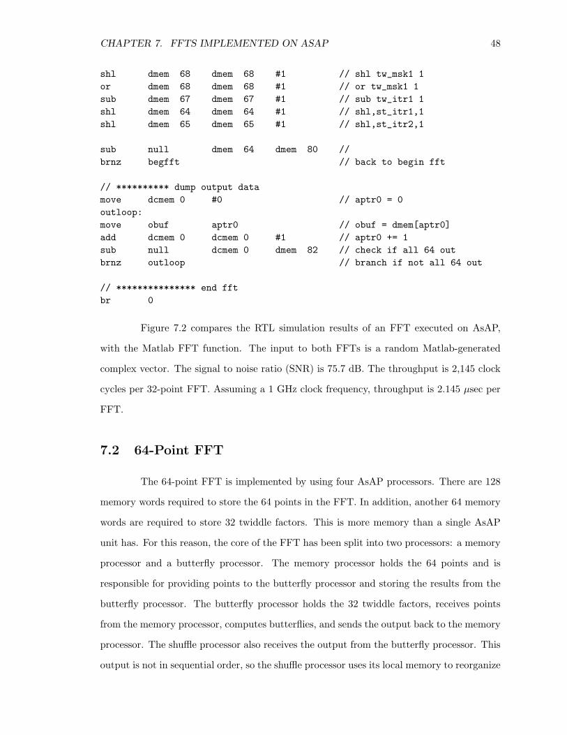
CHAPTER 7. FFTS IMPLEMENTED ON ASAP 48
shl dmem 68 dmem 68 #1 // shl tw_msk1 1
or dmem 68 dmem 68 #1 // or tw_msk1 1
sub dmem 67 dmem 67 #1 // sub tw_itr1 1
shl dmem 64 dmem 64 #1 // shl,st_itr1,1
shl dmem 65 dmem 65 #1 // shl,st_itr2,1
sub null dmem 64 dmem 80 //
brnz begfft // back to begin fft
// ********** dump output data
move dcmem 0 #0 // aptr0 = 0
outloop:
move obuf aptr0 // obuf = dmem[aptr0]
add dcmem 0 dcmem 0 #1 // aptr0 += 1
sub null dcmem 0 dmem 82 // check if all 64 out
brnz outloop // branch if not all 64 out
// *************** end fft
br 0
Figure 7.2 compares the RTL simulation results of an FFT executed on AsAP,
with the Matlab FFT function. The input to both FFTs is a random Matlab-generated
complex vector. The signal to noise ratio (SNR) is 75.7 dB. The throughput is 2,145 clock
cycles per 32-point FFT. Assuming a 1 GHz clock frequency, throughput is 2.145 µsec per
FFT.
7.2 64-Point FFT
The 64-point FFT is implemented by using four AsAP processors. There are 128
memory words required to store the 64 points in the FFT. In addition, another 64 memory
words are required to store 32 twiddle factors. This is more memory than a single AsAP
unit has. For this reason, the core of the FFT has been split into two processors: a memory
processor and a butterfly processor. The memory processor holds the 64 points and is
responsible for providing points to the butterfly processor and storing the results from the
butterfly processor. The butterfly processor holds the 32 twiddle factors, receives points
from the memory processor, computes butterflies, and sends the output back to the memory
processor. The shuffle processor also receives the output from the butterfly processor. This
output is not in sequential order, so the shuffle processor uses its local memory to reorganize
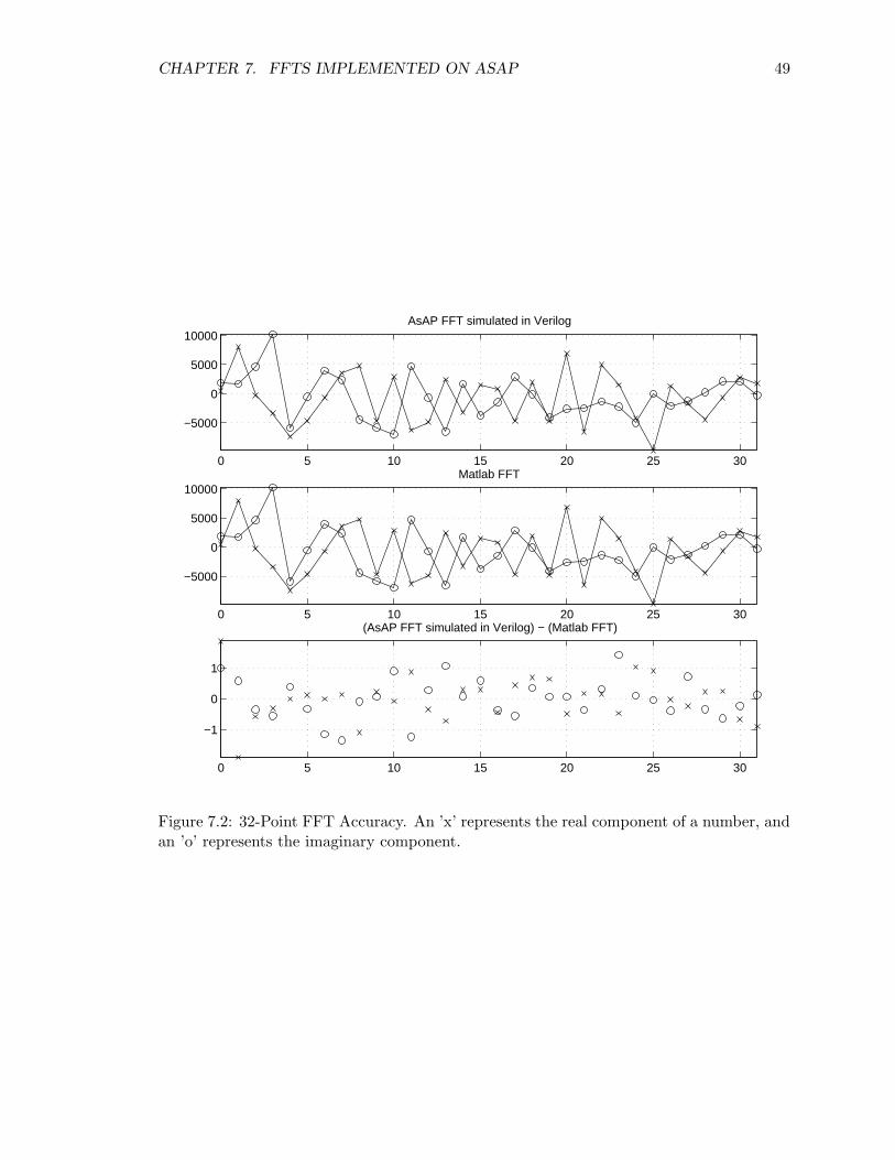
CHAPTER 7. FFTS IMPLEMENTED ON ASAP 49
0 5 10 15 20 25 30
−5000
0
5000
10000AsAP FFT simulated in Verilog
0 5 10 15 20 25 30
−5000
0
5000
10000Matlab FFT
0 5 10 15 20 25 30
−1
0
1
(AsAP FFT simulated in Verilog) − (Matlab FFT)
Figure 7.2: 32-Point FFT Accuracy. An ’x’ represents the real component of a number, andan ’o’ represents the imaginary component.
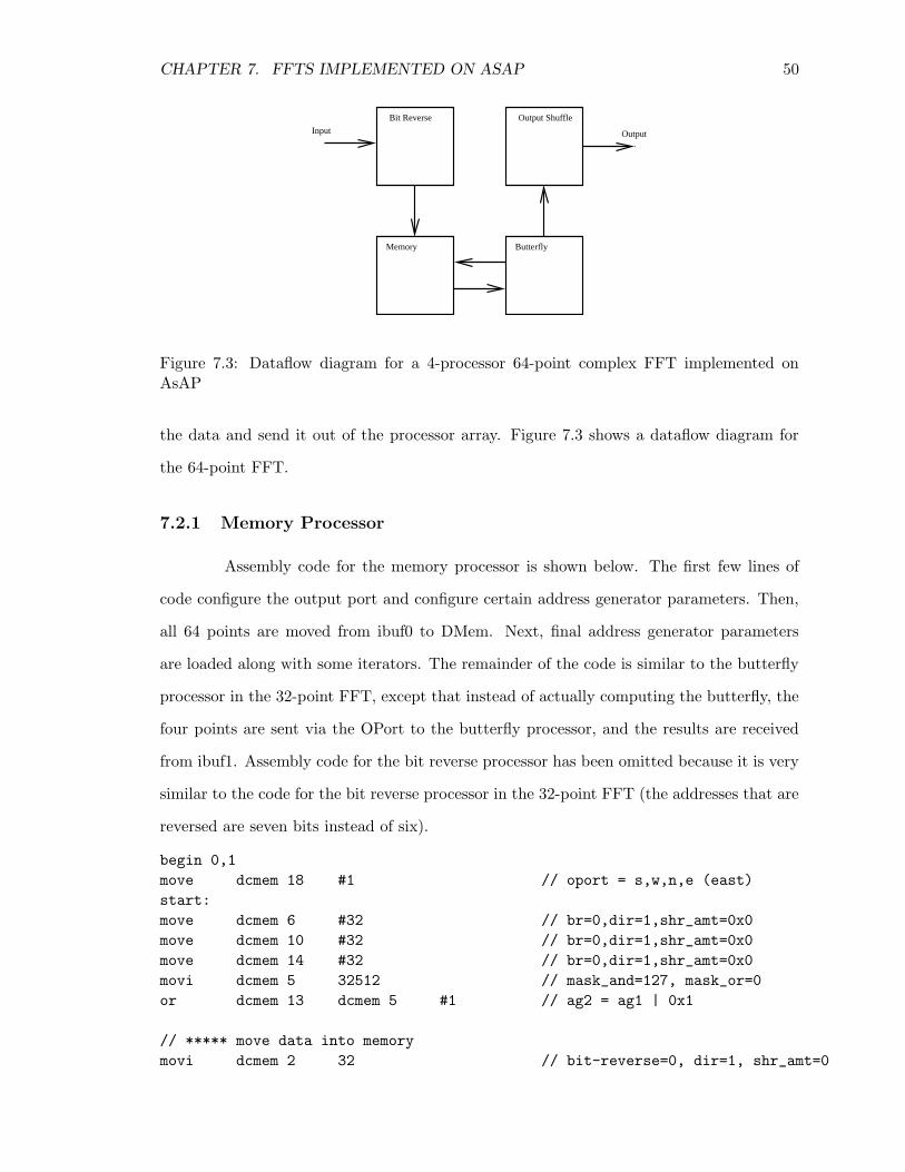
CHAPTER 7. FFTS IMPLEMENTED ON ASAP 50
Input Output
Memory Butterfly
Bit Reverse Output Shuffle
Figure 7.3: Dataflow diagram for a 4-processor 64-point complex FFT implemented onAsAP
the data and send it out of the processor array. Figure 7.3 shows a dataflow diagram for
the 64-point FFT.
7.2.1 Memory Processor
Assembly code for the memory processor is shown below. The first few lines of
code configure the output port and configure certain address generator parameters. Then,
all 64 points are moved from ibuf0 to DMem. Next, final address generator parameters
are loaded along with some iterators. The remainder of the code is similar to the butterfly
processor in the 32-point FFT, except that instead of actually computing the butterfly, the
four points are sent via the OPort to the butterfly processor, and the results are received
from ibuf1. Assembly code for the bit reverse processor has been omitted because it is very
similar to the code for the bit reverse processor in the 32-point FFT (the addresses that are
reversed are seven bits instead of six).
begin 0,1
move dcmem 18 #1 // oport = s,w,n,e (east)
start:
move dcmem 6 #32 // br=0,dir=1,shr_amt=0x0
move dcmem 10 #32 // br=0,dir=1,shr_amt=0x0
move dcmem 14 #32 // br=0,dir=1,shr_amt=0x0
movi dcmem 5 32512 // mask_and=127, mask_or=0
or dcmem 13 dcmem 5 #1 // ag2 = ag1 | 0x1
// ***** move data into memory
movi dcmem 2 32 // bit-reverse=0, dir=1, shr_amt=0

CHAPTER 7. FFTS IMPLEMENTED ON ASAP 51
movi dcmem 3 127 // start=0, end=127
movi dcmem 4 383 // stride=1, sml=1111111
movi dcmem 5 32512 // mask_and=127, mask_or=0
macc null #32 #4 // need to grab 128 data
rpt acc // repeat 128 times
move ag0pi ibuf0 // grab data from ibuf0
// ***** set up DAG0
movi dcmem 4 513 // stride =2, sml=1
// ***** set up DAG1
move dcmem 8 dcmem 4 // ag1 sml-str = ag0 sml-str
// ***** set up DAG2
move dcmem 12 dcmem 4 // ag2 sml-str = ag0 sml-str
// ***** set up DAG3
move dcmem 16 dcmem 4 // ag3 sml-str = ag0 sml-str
// ***** set up iterators
move dcmem 0 #1 // st_itr1 = stage0
move dcmem 1 #2 // st_itr2 = stage0
// *************** begin fft
begfft:
// ********** dag0-3 mask adjustment (for each stage)
// ********** also adjusts each end_addr (each stage)
movi dcmem 9 32512 // ag1 mask_and=127, mask_or=0
or dcmem 9 dcmem 9 dcmem 1 // ag1 mask_or = st_itr2
or dcmem 17 dcmem 9 #1 // ag3 mask_or = ag1 mask_or | 0x1
or dcmem 4 dcmem 4 dcmem 0 // ag0 sml = ago sml | st_itr1
move dcmem 8 dcmem 4 // ag1 sml-str = ag0 sml-str
move dcmem 12 dcmem 4 // ag2 sml-str = ag0 sml-str
move dcmem 16 dcmem 4 // ag3 sml-str = ag0 sml-str
macc null #63 #2
xor dcmem 3 dcmem 1 acc // ag0 end_addr=xor 126,st_itr2
xor dcmem 7 dcmem 1 acc // ag1 end_addr=xor 126,st_itr2
xor dcmem 11 dcmem 1 acc // ag2 end_addr=xor 126,st_itr2
xor dcmem 15 dcmem 1 acc // ag3 end_addr=xor 126,st_itr2
macc null #0 #0 // bf_itr = 0
// ********** begin butterfly
begbfly:
// ***** butterfly core
move obuf ag0 // move a_r to oport
move obuf ag2 // move a_i to oport
move obuf ag1 // move b_r to oport
move obuf ag3 // move b_i to oport
move ag0pi ibuf1 // receive a_r from ibuf1
move ag2pi ibuf1 // receive a_i from ibuf1
move ag1pi ibuf1 // receive b_r from ibuf1

CHAPTER 7. FFTS IMPLEMENTED ON ASAP 52
move ag3pi ibuf1 // receive b_i from ibuf1
mac null #1 #1 // bf_itr += 1
sub null acc #32 // counting to 32
brn begbfly // back to begin butterfly
shl dcmem 0 dcmem 0 #1 // shl st_itr1,1
shl dcmem 1 dcmem 1 #1 // shl st_itr2,1
macc null #8 #8 // slt with 64
sub null dcmem 0 acc // stage is over !
brn begfft // back to begin fft
br start // back to start
end
7.2.2 Butterfly Processor
Assembly code for the butterfly processor is shown below. After several lines of
initialization code, the code for butterfly calculation begins. Although this processor only
computes butterflies, it still keeps track of which butterfly is being executed, because it
must supply the corresponding twiddle factor from its own memory. Addresses for the
twiddle factors are generated manually and twiddle factors are accessed using aptr0 and
aptr2. The butterfly core is slightly different from the 32-point FFT because in this case,
the data is returned in a certain order. To save two instructions, the data can be returned
to the memory processor in the order that it is computed. During the first five stages
of butterflies, this processor sends data back only to the memory processor. In the sixth
stage, the OPort configuration is changed to send data to both the memory processor and
the shuffle processor. This is done to save cycles. Instead of having to store the results from
the final stage and re-read them in order, the results are passed on to the shuffle processor.
It is possible for the butterfly processor to always send data to both the memory processor
and the shuffle processor. However, butterfly outputs from the first five stages are useless
to the shuffle processor. Also, a large enough energy savings exists to make it beneficial to
only send useful data.
begin 1,1
move dcmem 18 #4 // oport = s,w,n,e (west)
// ***** begin a whole fft
move dmem 4 #0 // st_itr1 = 0
move dmem 7 #6 // tw_shamt = 6

CHAPTER 7. FFTS IMPLEMENTED ON ASAP 53
move dmem 8 #0 // tw_msk1 = 0
begst:
// ***** begin a stage
move dmem 6 #0 // bf_itr = 0
// ***** begin a butterfly
begbfly:
move dmem 10 ibuf0 // get a_r
move dmem 11 ibuf0 // get a_i
move dmem 12 ibuf0 // get b_r
move dmem 13 ibuf0 // get b_i
and dcmem 0 dmem 6 dmem 8 // aptr0 = bf_itr & tw_msk
shl dcmem 0 dcmem 0 dmem 7 // shl aptr0 tw_shamt
or dcmem 0 dcmem 0 dmem 9 // twiddles are in upper 64
or dcmem 1 dcmem 0 #1 // address for tw_i
// ***** begin butterfly core
macc null aptr0 dmem 12 // mac w_r,b_r
sub dmem 14 #0 aptr2 // mult t1 w_i,-1
mac null dmem 14 dmem 13 // mac t1,b_i
accshr #14 // accshr #14
addinc dmem 14 dmem 10 acc // add 1 t1,a_r,acc
subh dmem 15 dmem 10 acc // sub 1 t2,a_r,acc
// *****
macc null aptr2 dmem 12 // mac twid_i,b_r
mac null aptr0 dmem 13 // mac twid_r,b_i
accshr #14 // accshr #14
subh dmem 13 dmem 11 acc // store b_i
addinc dmem 11 dmem 11 acc // store a_i
move dmem 10 dmem 14 // store a_r
move dmem 12 dmem 15 // store b_r
// ***** end butterfly core
move obuf dmem 10 // output a_r
move obuf dmem 11 // output a_i
move obuf dmem 12 // output b_r
move obuf dmem 13 // output b_i
add dmem 6 dmem 6 #1 // increment bf_itr
sub null dmem 6 #32 // 32 butterflies per stage
brn begbfly // back to begin a butterfly
// ***** end a butterfly
shl dmem 8 dmem 8 #1 // shl tw_msk1 #1
or dmem 8 dmem 8 #1 // or tw_msk1 #1
sub dmem 7 dmem 7 #1 // sub tw_shamt #1
add dmem 4 dmem 4 #1 // add st_itr1 #1
sub null dmem 4 #5 // check if time for output
brz onobuf

CHAPTER 7. FFTS IMPLEMENTED ON ASAP 54
cont:
sub null dmem 4 #6 // 6 stages in 64 pt fft
brn begst // back to begin a stage
// ***** end a stage
br 0 // back to begin a whole fft
onobuf:
move dcmem 18 #6
br cont
// ***** end a whole fft
end
7.2.3 Shuffle Processor
Assembly code for the shuffle processor is shown below. The shuffle processor
receives the final output for the FFT in an interleaved fashion. This can be observed in
Fig. 2.3. As a result, the first point received is sent to output, while the second point
received is stored for final output. This is repeated for all 32 pairs of points.
begin 1,0
move dcmem 18 #1 // oport = s,w,n,e (east)
// ***** begin store and output final 128
movi dcmem 0 64 // start storing at 64
loopso:
move obuf ibuf0 // first 2 go out
move obuf ibuf0 //
move aptr0 ibuf0 // 2nd 2 go in to memory
add dcmem 0 dcmem 0 #1 // increment aptr0
move aptr0 ibuf0 // get 2nd datum
add dcmem 0 dcmem 0 #1 // increment aptr0 again
sub null dcmem 0 #0 // when dcmem rolls to 0, done
brnz loopso
// ***** begin output last 64
movi dcmem 2 32 // bit-reverse=0, dir=1, shr_amt=0
movi dcmem 3 16511 // start=64, end=127
movi dcmem 4 383 // stride=1, sml=1111111
movi dcmem 5 32512 // mask_and=127, mask_or=0
macc null #8 #8 // need to move 64 data
rpt acc // repeat 64 times
move obuf ag0pi // move it out
br 0

CHAPTER 7. FFTS IMPLEMENTED ON ASAP 55
0 10 20 30 40 50 60
−5000
0
5000
AsAP FFT Simulated in Verilog
0 10 20 30 40 50 60
−5000
0
5000
Matlab FFT
0 10 20 30 40 50 60
−1
0
1
(AsAP FFT Simulated in Verilog) − (Matlab FFT)
Figure 7.4: 64-Point FFT Accuracy. An ’x’ represents the real component of a number, andan ’o’ represents the imaginary component.
Figure 7.4 shows the simulation output for the 64-point FFT, compared to the
Matlab FFT function. The SNR is 73.3 dB. The throughput is 7,360 clock cycles per
64-point FFT.
7.2.4 Eight Processor Version
The 64-point FFT is also implemented in an eight-processor version. There are
three memory processors, three butterfly processors, a bit-reverse processor, and a shuffle
processor. Figure 7.5 shows a dataflow diagram for the eight-processor 64-point FFT. Each
memory-butterfly processor pair computes only two stages of butterflies instead of all six.
Code for the eight processor 64-point FFT is omitted, because it is a practical extension of
the four-processor 64-point FFT. At the cost of more processors, throughput is improved.
The throughput is 3,515 clock cycles per 64-point FFT for the eight-processor version. At

CHAPTER 7. FFTS IMPLEMENTED ON ASAP 56
Memory Butterfly
Memory Butterfly
Memory Butterfly
Input
Bit ReverseOutput
Shuffle
Figure 7.5: Dataflow diagram for an eight-processor 64-point complex FFT implementedon AsAP
a 1 GHz clock frequency, throughput is 3.515 µsec per FFT.
7.3 1024-Point FFT
The 1024-point FFT is implemented with the Cached FFT Algorithm. There are
10 stages in a normal radix-2 1024-point FFT. We chose to implement two epochs, so that
each epoch is composed of five passes. Each epoch can be implemented with 32-point FFTs.
Although there will be 32 groups (equivalent to 32 32-point FFTs), there do not have to be
32 processors for each epoch. In the smallest case, only one 32-point FFT engine is needed
for each epoch, and the 32-point FFTs are executed serially.
In such a configuration, there are six AsAP processors used, in addition to three
large memories. Two processors are dedicated to computing 32-point FFTs (one per epoch).
One processor and one memory are dedicated to bit-reversal. Two processors and two
memories are used to perform the memory shuffles at the end of each epoch. The sixth
processor generates twiddle factors for the second epoch butterfly processor. The first
epoch butterfly processor does not need a separate processor to produce twiddle factors.
Figure 7.6 shows the AsAP dataflow for this FFT implementation.
A 1024-point FFT requires 2048 memory entries for data points. To address so
much memory, 11-bit addresses are required. Address generators and address pointers in
AsAP processors cannot address such a large memory space. In addition they are not

CHAPTER 7. FFTS IMPLEMENTED ON ASAP 57
OutputInputBit Reverse Epoch1 Shuffle
Wn Generator
32 Pt. FFT Epoch0 Shuffle 32 Pt. FFT
4kx16 4kx16 4kx16
Figure 7.6: Dataflow diagram for a 6-processor 1024-point complex FFT implemented onAsAP
connected to address external memory. However, since the Cached FFT is being used,
11-bit addresses are not always required. The processors that execute 32-point FFTs do
not address external memory, and use address generators, like the previous implementation
of the 32-point FFT. The processors that access the large memories still need to generate
11-bit addresses when they execute reads or writes. Table 7.1 shows the memory access
patterns for a 32-point Cached FFT. Table 7.2 shows the memory access patterns for the
shuffle processors.
7.3.1 Bit Reverse Processor
Assembly code for the bit reverse processor is shown below. This processor commu-
nicates with a large memory to the north of itself. Also, it communicates with the 32-point
FFT processor for epoch0, which is to the east. In addition, it is the input processor, where
data is fed into the array. In order to send data to the memory without sending data to
the 32-point FFT processor (or vice versa), this processor enables only one OPort direction
at a time. This processor reads and outputs one datum at a time by probing the input

CHAPTER 7. FFTS IMPLEMENTED ON ASAP 58
Epoch Pass Butterfly WN
Number Number Address Address
0 0 c3c2c1c0IJ W 000000000J1024
1 c3c2c1Ic0J W c000000000J1024
2 c3c2Ic1c0J W c1c00000000J1024
3 c3Ic2c1c0J W c2c1c0000000J1024
4 Ic3c2c1c0J W c3c2c1c000000J1024
1 0 c3c2c1c0IJ W g4g3g2g1g00000J1024
1 c3c2c1Ic0J W c0g4g3g2g1g0000J1024
2 c3c2Ic1c0J W c1c0g4g3g2g1g000J1024
3 c3Ic2c1c0J W c2c1c0g4g3g2g1g00J1024
4 Ic3c2c1c0J W c3c2c1c0g4g3g2g1g0J1024
Table 7.1: Real and Imaginary addresses for a two-epoch 1024-point Cached FFT [4]. Theseaddresses are used by 32-point FFT engines to compute each group in the Cached FFT.
Epoch Butterfly Memory
Number Address Address
0 * * * * * J g4g3g2g1g0 ∗ ∗ ∗ ∗ ∗ J
1 * * * * * J ∗ ∗ ∗ ∗ ∗g4g3g2g1g0J
Table 7.2: Real and Imaginary addresses for memory shuffle in a 1024-point Cached FFT[4]. These addresses are used by shuffle processors to load and store data between epochs.

CHAPTER 7. FFTS IMPLEMENTED ON ASAP 59
FIFOs and the OPort to check for vacancy. This is accomplished with “BRF0”, “BRF1”,
and “BROB” instructions, which check ibuf0, ibuf1, and OPort respectively. Polling the
FIFOs in this manner lets a processor check if a FIFO is full without stalling. This allows
the processor to do other useful work if the FIFO is full or empty. In addition, memory is
double-buffered (into two banks), so that twice as much memory is being used, but reads
from and writes to memory can be interleaved. This speeds up the FFT. One bank is used
to store data to memory, while data is read from the other bank. Once one bank is full and
the other is empty, they exchange roles. Bank 0 starts at address 0 and ends at address
2047. Bank 1 starts at address 2048 and ends at address 4095.
Bit reversal of addresses is accomplished by using the “BTRV” instruction, which
reverses all 16 bits of a word. In order to address only 11 bits, the result of “BTRV” is
shifted right by five bits. Input data is stored to memory using bit reversal in the “getone”
subroutine. After all 2048 data have been written to memory, data is read from memory
and sent to the OPort.
begin 0,0
start:
move dcmem 18 #1 // obuf = s,w,n,e (east)
movi dmem 20 2048 // store to bank 1
movi dmem 21 0 // dump from bank 0
movi dmem 22 0 // want to grab an entire fft
movi dmem 23 2048 // don’t want to send yet
movi dmem 24 32768 // start at zero (msb for write)
or dmem 24 dmem 24 dmem 10 // store to bank 1
movi dmem 26 0 // real_imag_or_mask = 0
// ***** send a datum if fft not finished and obuf not full
startsend:
sub dmem 30 dmem 23 dmem 10 // check if all 2048 sent
brz startget // all 2048 sent, try getting data
move dcmem 18 #1 // obuf = s,w,n,e (east)
brob sendone // send if obuf ready (18)
// make sure obuf config is east
donesend:
// ***** get a datum if fft not finished and ibuf not empty
startget:
sub dmem 31 dmem 22 dmem 10 // check if all 2048 gotten
brz wait // if so, go to wait
brf0 getone // else, get one if ibuf0 ready

CHAPTER 7. FFTS IMPLEMENTED ON ASAP 60
doneget:
wait:
or null dmem 30 dmem 31 // first, check if both done
brz swapbanks // if so, time to swap banks, else...
xor dmem 32 dmem 22 dmem 23 // check if ctr_get = ctr_send
sub null dmem 32 dmem 10 // subtract away 2048 to check if done
brnz doneswap // if not done, go to doneswap
brf1 getfinal // get last datum from ibuf1
br doneswap // done
getfinal:
move dcmem 18 #1 // obuf = s,w,n,e (east)
move obuf ibuf1 // from fifo1 to output
doneswap:
// ***** try the whole thing again by going back to startsend
br startsend
sendone: // output a data (sequential, not br)
move dcmem 18 #1 // obuf = s,w,n,e (east)
move obuf ibuf1 // from fifo1 to output
move dcmem 18 #2 // obuf = s,w,n,e (north)
or obuf dmem 23 dmem 21 // read from mem with ctr_send
add dmem 23 dmem 23 #1 // incremement ctr_send
br donesend
getone: // store a data (with bit-reversal)
move dcmem 18 #2 // obuf = s,w,n,e (north) store to mem
btrv dmem 33 dmem 24 // dmem33 holds bit reversed dmem24
shr dmem 33 dmem 33 #5 // 1k fft keeps 11 bit for addr
or dmem 33 dmem 33 dmem 13 // msb = 1 for write
or dmem 33 dmem 33 dmem 20 // select bank to store to
or obuf dmem 33 dmem 26 // control word to mem (write)
// dmem26 is real/imag bit (lsb)
move obuf ibuf0 // store input to mem (write)
add dmem 22 dmem 22 #1 // ctr_store++
xor dmem 26 dmem 26 #1 // flip real/imag bit
brnz skipinc // only increment store_addr 1/2 time
add dmem 24 dmem 24 #1 // increment addr_get
skipinc:
br doneget // finished getting one datum
swapbanks:
brf1 getlast
contswap:
xor dmem 20 dmem 20 dmem 10 // swap banks for store
xor dmem 21 dmem 21 dmem 10 // swap banks for dump
CHAPTER 7. FFTS IMPLEMENTED ON ASAP 61
move dmem 22 #0 // clear ctr_get (one fft done)
move dmem 23 #0 // clear ctr_send count (one fft done)
move dmem 24 #0 // clear store address (msb for write)
or dmem 24 dmem 24 dmem 20 // set store bank
move dmem 26 #0 // real_imag_or_mask = real
move dcmem 18 #2 // obuf = s,w,n,e (north)
or obuf dmem 23 dmem 21 // read from mem with ctr_send
add dmem 23 dmem 23 #1 // incremement ctr_send
br doneswap // could go straight to startone
getlast:
move dcmem 18 #1 // obuf = s,w,n,e (east)
move obuf ibuf1 // from fifo1 to output
nop
brf1 getlast // if ibuf1 not empty, get last datum
br contswap // done
end
Assembly code for the first-epoch FFT engine is identical to the butterfly processor
in the 32-point FFT presented earlier in this chapter.
7.3.2 First-Epoch Shuffle Processor
For the first-epoch shuffle processor, assembly code is shown below. This processor
reads data from the first-epoch FFT engine, stores it to a large memory with shuffled
addresses, and then reads data (sequentially) from the same memory to send the results to
the second-epoch FFT engine. It also uses double-buffering and probes FIFOs. The first
few lines of code initializes constants. Data is read from ibuf0 and written to memory using
shuffled addresses. The shuffled addresses are dictated by the patterns in Table 7.2. Again,
reads from ibuf0 and writes to OPort are interleaved and processors never stall. This is
better than other implementations where processors stall while waiting for large blocks of
data, even though other useful work can be done.
begin 2,0
start:
move dcmem 18 #1 // obuf = s,w,n,e (east)
movi dmem 20 2048 // store to bank 1
movi dmem 21 0 // dump from bank 0
movi dmem 22 0 // want to grab an entire fft
movi dmem 23 2048 // don’t want to send yet
movi dmem 24 32768 // start at zero (msb for write)

CHAPTER 7. FFTS IMPLEMENTED ON ASAP 62
or dmem 24 dmem 24 dmem 10 // store to bank 1
movi dmem 26 0 // real_imag_or_mask = 0
// ***** send a datum if fft not finished and obuf not full
startsend:
sub dmem 30 dmem 23 dmem 10 // check if all 2048 sent
brz startget // all 2048 sent, try storing
move dcmem 18 #1 // obuf = s,w,n,e (east)
brob sendone // send if obuf ready
// make sure obuf config is east
donesend:
// ***** get a datum if fft not finished and ibuf not empty
startget:
sub dmem 31 dmem 22 dmem 10 // check if all 2048 gotten
brz wait // if so, go to wait
brf0 getone // store if ibuf ready
doneget:
wait:
or null dmem 30 dmem 31 // first, check if both done
brz swapbanks // if so, time to swap banks, else...
xor dmem 32 dmem 22 dmem 23 // check if ctr_get = ctr_send
sub null dmem 32 dmem 10 // subtract away 2048 to check if done
brnz doneswap // if not done, go to doneswap
brf1 getfinal // get last datum from ibuf1
br doneswap // done
getfinal:
move dcmem 18 #1 // obuf = s,w,n,e (east)
move obuf ibuf1 // from fifo1 to output
doneswap:
// ***** try the whole thing again by going back to startsend
br startsend
sendone: // output a data
move dcmem 18 #1 // obuf = s,w,n,e (east)
move obuf ibuf1 // from fifo1 to output
move dcmem 18 #2 // obuf = s,w,n,e (north)
or obuf dmem 23 dmem 21 // read from mem with ctr_send
add dmem 23 dmem 23 #1 // incremement ctr_send
br donesend
getone: // store a data
move dcmem 18 #2 // obuf = s,w,n,e (north) store to mem
or obuf dmem 24 dmem 26 // control word to mem (write)
move obuf ibuf0 // store input to mem (real)

CHAPTER 7. FFTS IMPLEMENTED ON ASAP 63
add dmem 22 dmem 22 #1 // ctr_store++
xor dmem 26 dmem 26 #1 // flip real_imag_or_mask
brnz chkcnt // only increment store_addr 1/2 time
add dmem 24 dmem 24 dmem 12 // store_addr += 64
chkcnt:
and null dmem 22 #63 // check if lower 6 bits are zero
brnz doneget // not done with all 32 PTs
and dmem 24 dmem 24 dmem 14 // clear count
or dmem 24 dmem 24 dmem 13 // write msb for store
or dmem 24 dmem 24 dmem 20 // reset bank
add dmem 24 dmem 24 #2 // store_addr += 2
br doneget
swapbanks:
brf1 getlast
contswap:
xor dmem 20 dmem 20 dmem 10 // swap banks for store
xor dmem 21 dmem 21 dmem 10 // swap banks for dump
move dmem 22 #0 // clear ctr_get (one fft done)
move dmem 23 #0 // clear ctr_send count (one fft done)
movi dmem 24 32768 // clear store address (msb for write)
or dmem 24 dmem 24 dmem 20 // set store bank
move dmem 26 #0 // real_imag_or_mask = real
move dcmem 18 #2 // obuf = s,w,n,e (north)
or obuf dmem 23 dmem 21 // read from mem with ctr_send
add dmem 23 dmem 23 #1 // incremement ctr_send
br doneswap // could go straight to startone
getlast:
move dcmem 18 #1 // obuf = s,w,n,e (east)
move obuf ibuf1 // from fifo1 to output
nop
brf1 getlast // if ibuf1 not empty, get last datum
br contswap // done
end
7.3.3 Second-Epoch Twiddle Factor Generator Processor
The second-epoch FFT engine is different from the first-epoch FFT engine. Dataflow
for both FFTs is the same, but in the second epoch, each group has a unique set of twiddle
factors. There are 512 twiddle factors to choose from in the 1024-point FFT, and all are
used at least once in the second-epoch FFT. There are many ways to reduce the amount of

CHAPTER 7. FFTS IMPLEMENTED ON ASAP 64
memory necessary for twiddle factors [19, 20]. Instead of reserving memory space for all of
the twiddle factors, we chose to allocate a processor to compute them as they are needed.
The method for computing the twiddle factors makes use of a mathematical property of
exponents. Equation 7.1 shows how one twiddle factor can be computed from two others.
WA+BN = WA
N WBN (7.1)
For the 1024-point FFT, W 0N through W 511
N are necessary. We chose to store W 0N through
W 31N in addition to the series W 0
N , W 32N , W 64
N , W 96N ... W 448
N , W 480N . With these twiddle
factors available, any of the required twiddle factors can be generated with one complex
multiplication. Although there is error introduced by computing the twiddle factors instead
of storing them, this implementation greatly reduces the number of processors in the array.
It requires only 48 twiddle factors, or 96 DMem locations in the twiddle factor generator
processor. In this case, there is a trade-off between area (or memory space) and accuracy.
Assembly code for the second-epoch twiddle factor generator processor is shown
below. DMem locations 0 through 63 hold W 0N through W 31
N . DMem locations 64 through 95
hold the series of nonconsecutive twiddle factors. The twiddle factor generator keeps track
of which group is being computed, since different groups have different twiddle factors.
begin 1,1
move dcmem 18 #2 // obuf = s,w,n,e (north)
move dmem 100 #0 // g_ctr = 0 ( group counter )
forgctr:
move dmem 104 #5 // 1k fft b_shramt = 5
move dmem 101 #0 // pass_ctr = 0
forpassctr:
move dmem 102 #0 // bfly_ctr = 0
forbflyctr:
shl dmem 105 dmem 102 dmem 104 // tmp1 = shl bfly_ctr, b_shramt
and dcmem 0 dmem 105 #31 // tmp3 = and tmp3,1023
or dcmem 1 dcmem 0 #1
move obuf aptr0
move obuf aptr2
add dmem 102 dmem 102 #1 // bfly_ctr++
sub null dmem 102 #16 // 1k fft, 2 epoch, 32 pt fft / epoch
brnz forbflyctr
CHAPTER 7. FFTS IMPLEMENTED ON ASAP 65
add dmem 101 dmem 101 #1 // pass_ctr++
sub dmem 104 dmem 104 #1 // b_shramt--
sub null dmem 101 #5 // 1k fft, 2 epoch, 5 passes / epoch
brnz forpassctr
add dmem 100 dmem 100 #1 // g_ctr ++
sub null dmem 100 #32 // 1k fft, 2 epoch, 32 groups
brnz forgctr
br 0
end
Assembly code for the second-epoch FFT engine is omitted. It is similar to the
first-epoch FFT engine, except it acquires twiddle factors from the twiddle factor generator
instead of storing them locally. Also, the second-epoch shuffle processor is nearly identical
to the first-epoch shuffle processor. It only has a different configuration for the bits in its
memory addresses.
Figure 7.7 shows the comparison between the AsAP-implemented FFT and the
Matlab FFT function. The SNR is 64.4 dB. The throughput is 101,340 cycles per 1024-
point FFT. At a 1 GHz clock frequency, throughput is 101 µsec per FFT.
Table 7.3 shows the utilization of each active processor in the array for the differ-
ent FFTs simulated on AsAP. There are three states that any processor can be in: stalled
waiting for input, stalled waiting to output, and executing program code. Utilization is
computed as ExecuteCycles/TotalCycles. In the 1024-point FFT, utilization for proces-
sors that probe FIFOs instead of stalling on FIFOs is 100%. This is because these processors
are always executing code, even if most of the execution is only polling FIFOs. The esti-
mated utilization based on the non-polling model of this FFT is: 25.1% for the Bit Reverse
Processor, 29.6% for the Epoch0 FFT engine, and 29.1% for the Epoch1 FFT engine. These
numbers reflect the time these processors do not spend polling FIFOs.
Another model for the 1024-point FFT has been investigated, but not simulated.
Figure 7.8 shows a 25-processor model in which there are eight processors executing 32-point
FFTs instead of only two. The described six-processor model for the 1024-point FFT can
complete one FFT every 101,340 clock cycles. The 25-processor model has four times as
many FFT engines. We estimate one FFT to be completed every 30,000 clock cycles. This

CHAPTER 7. FFTS IMPLEMENTED ON ASAP 66
0 100 200 300 400 500 600 700 800 900 1000−2000
−1000
0
1000
2000
AsAP FFT Simulated in Verilog
0 100 200 300 400 500 600 700 800 900 1000−2000
−1000
0
1000
2000
Matlab FFT
0 100 200 300 400 500 600 700 800 900 1000
−2
−1
0
1
(AsAP FFT Simulated in Verilog) − (Matlab FFT)
Figure 7.7: 1024-Point FFT Accuracy. An ’x’ represents the real component of a number,and an ’o’ represents the imaginary component.

CH
AP
TE
R7.
FFT
SIM
PLE
ME
NT
ED
ON
ASA
P67
FFT Processor Processor Input Output Execute Total Utilization
Length ID Name Stall Stall Cycles Cycles
Cycles Cycles
32-Pt. 0,0 Bit Reverse 0 4975 1461 6436 22.7%
1,0 Butterfly 221 0 0 6436 100.0%
64-Pt. 0,0 Bit Reverse 0 20322 1759 22081 8.0%
0,1 Memory 14976 0 7105 22081 32.2%
1,1 Butterfly 5770 0 16311 22081 73.9%
1,0 Shuffle 21093 0 988 22081 4.4%
1024-Pt. 0,0 Bit Reverse 0 0 306415 306415 100.0% *
1,0 32 Pt. FFT Epoch 0 47771 48434 210210 306415 68.6%
2,0 Epoch 0 Shuffle 0 0 306415 306415 100.0% *
3,0 32 Pt. FFT Epoch 1 69654 47043 189718 306415 61.9%
3,1 Wn Generator 0 117991 188424 306415 61.5%
4,0 Epoch 1 Shuffle 0 0 306415 306415 100.0% *
Table 7.3: Processor Utilization for FFT Applications. Utilization with a “*” is 100.0% because this processor probes FIFOs instead ofstalling on FIFOs

CHAPTER 7. FFTS IMPLEMENTED ON ASAP 68
32 Pt. FFT
32 Pt. FFT
32 Pt. FFT
32 Pt. FFT
32 Pt. FFT
32 Pt. FFT
32 Pt. FFT
32 Pt. FFT
Bit Reverse
Data Forward
Data Forward
Data Forward Data Forward
Data Forward
Data Forward
Data Forward Data Forward
Data Forward
Data Forward
Data Forward
Epoch0 Shuffle Epoch1 Shuffle
Wn Generate
Data Forward
Data Forward
Data Forward
Wn Generate
Wn Generate
Wn Generate
Input Output
4kx16 4kx16 4kx16
Figure 7.8: Dataflow diagram for a 25-processor 1024-point complex FFT.
projection is supported by the fact that both Shuffle processors in the six-processor model
are utilized only 30% of the time. The Shuffle processors can supply up to three times as
much data without saturating.
69
Chapter 8
Conclusion
8.1 Contributions
The contributions of this work are mapping, coding and testing of fixed-point
radix-2 FFTs to the AsAP architecture. The FFTs mapped include 32-point, 64-point, and
1024-point. Also, design and simulation of hardware data address generators are presented.
Software tools to produce binary code for configuration and execution of algorithms were
created during the course of the research.
8.2 Future Work
There are two primary categories where future effort can be applied to this work.
First, assembly code for the FFTs must be scheduled once a pipelined model of AsAP is
available. Second, the performance of the 1024-point FFT can be improved.
8.2.1 Assembly Code for a Pipelined AsAP Architecture
When a complete pipelined RTL model for the AsAP architecture is available,
scheduling of assembly code becomes necessary. In pipelined processors, data dependencies
and structural hazards often limit how instructions are executed. It is favorable to imple-
ment a software scheduler that transforms current assembly code into pipelined assembly
code for AsAP. The alternative is for the programmer to schedule each program by hand,

CHAPTER 8. CONCLUSION 70
which is tedious. Regardless of which method is used, the need to schedule code often
decreases performance. This is because ”NOP” instructions must be used if re-ordering of
code does not alleviate a dependency or hazard. Various performance optimizations can be
made to the assembly code to offset such a loss.
8.2.2 Performance Optimizations
Assembly code written for the three FFTs implemented on AsAP was not op-
timized for performance. Although performance was taken into account during mapping
and coding of the algorithms, there remains work to be done in this realm. The principal
example is the 1024-point FFT. There are six processors performing computation for this
FFT. The AsAP project was designed to have tens or hundreds of processors on a single
chip. It is possible to find better mappings like Fig. 7.8, which make use of more processors
on the array to improve performance. Also, there are optimizations that can be made to
the FFT algorithm itself to improve performance [19].

71
Bibliography
[1] A. V. Oppenheim and R. W. Schafer. Discrete-Time Signal Processing. Prentice-Hall,Englewood Cliffs, NJ, 1989.
[2] B.P. Lathi. Signal Processing and Linear Systems. Oxford University Press, New York,New York, 1998.
[3] J. W. Cooley and J. W. Tukey. An algorithm for the machine calculation of complexfourier series. In Math. of Comput., volume 19, pages 297–301, April 1965.
[4] Bevan. M. Baas. An Approach to Low-Power, High-Performance Fast Fourier Trans-
form Processor Design. PhD thesis, Stanford University, Stanford, CA, USA, 1999.
[5] S. He and M. Torkelson. Design and implementation of a 1024-point pipeline FFTprocessor. In IEEE Custom Integrated Circuits Conference, pages 131–134, May 1998.
[6] Bevan M. Baas. A low-power, high-performance, 1024-point FFT processor. IEEE
Journal of Solid-State Circuits, 34(3):380–387, March 1999.
[7] Moon-Key Lee, Kyung-Wook Shin, and Jang-Kyu Lee. A VLSI array processor for 16-point FFT. IEEE Journal of Solid-State Circuits, 26(9):1286–1292, September 1991.
[8] K. W. Shin and M. K. Lee. A massively parallel VLSI architecture suitable for high-resolution FFT. In IEEE International Symposium on Circuits and Systems, volume 5,pages 3050–3053, June 1991.
[9] Yongjun Peng. A parallel architecture for VLSI implementation of FFT processor. InIEEE International Conference on ASIC, volume 2, pages 748–751, October 2003.
[10] A. H. Kamalizad, C. Pan, and N. Bagherzadeh. Fast parallel FFT on a reconfigurablecomputation platform. In Computer Architecture and High Performance Computing,volume 15, pages 254–259, November 2003.
[11] Ujval Kapasi, William J. Dally, Scott Rixner, John D. Owens, and Brucek Khailany.The Imagine stream processor. In Proceedings 2002 IEEE International Conference on
Computer Design, pages 282–288, September 2002.
[12] D. Patterson, T. Anderson, N. Cardwell, R. Fromm, K. Keeton, C. Kozyrakis,R. Thomas, and K. Yelick. A case for intelligent RAM. IEEE Micro, 17:34–44, March1997.
[13] R. Thomas and K. Yelick. Efficient FFTs on iram. In First Workshop on Media
Processors and DSPs, November 1999.

BIBLIOGRAPHY 72
[14] FFT Processor Info Page. http://www-star.stanford.edu/~bbaas/fftinfo.html.
[15] Bevan M. Baas. A parallel programmable energy-efficient architecture forcomputationally-intensive DSP systems. In Signals, Systems and Computers, 2003.
Conference Record of the Thirty-Seventh Asilomar Conference on, November 2003.
[16] Ryan W. Apperson. A dual-clock FIFO for the reliable transfer of high-throughputdata between unrelated clock domains, 2004.
[17] Matlab. http://www.mathworks.com/products/matlab/.
[18] NC–Verilog. http://www.cadence.com/products/functional_ver/nc-verilog/
index.aspx.
[19] R. Meyer and K. Schwarz. FFT implementation on dsp chips theory and practice. InInternational Conference on Acoustics, Speech, and Signal Processing, volume 3, pages1503–1506, April 1990.
[20] M. Hasan and T. Arslan. Scheme for reducing size of coefficient memory in FFTprocessor. IEEE Journal of Electronics Letters, 38(4):163–164, February 2002.
[21] L. R. Rabiner and B. Gold. Theory and Application of Digital Signal Processing.Prentice-Hall, Englewood Cliffs, NJ, 1975.