Far-Infrared Single-Photon Detectors Fabricated in Double
22
7 Far-Infrared Single-Photon Detectors Fabricated in Double-Quantum-Well Structures Takeji Ueda and Susumu Komiyama The University of Tokyo Japan 1. Introduction Sensitive infrared (IR) detectors are key elements for both fundamental research and applications, and development of sensitive IR detectors is one of intensive research subjects in resent years (Rogalski, 2002; Tidrow, 2000). The activities are motivated by both basic and applied research fields (Prochazka, 2005; Rogalski, 2002). For certain applications, an ultimately high sensitivity reaching a photon-counting level is indispensable; for instance, passive high-resolution microscopy, catching IR photons spontaneously emitted by a living cell or a small number of biomolecules, may be accessible only with such ultimately sensitive detectors. Photon-counters are routinely used in visible and near infrared regions (Prochazka, 2005). In the long-wavelength range (nj > 10 Ǎm, frequencies lower than 30 THz), called terahertz (THz) region, however, photon energies are far smaller (hǎ < 124 meV for nj > 10 Ǎm) and the single-photon detection is no longer trivial. Nevertheless, the THz region is one of the richest areas of spectroscopy of matters, encompassing the rotational spectra of molecules, vibrational spectra of molecules, liquids and solids, and the electron energy spectra in semiconductor nanostructures and superconducting energy gap in metals. Hence, sensitive microscopy of matters with high spatial resolution in this spectral region would provide a unique powerful tool for investigation of matters. Sensitive observation is also strongly demanded in astrophysics (Nakagawa et al, 2007). In the last decade, a variety of novel detection schemes have been proposed (Astaviev et al., 2002; Day et al., 2003; Hashiba et al., 2006; Komiyama et al., 2000; Schoelkopf et al., 1999; Wei et al., 2008). Among them, only semiconductor quantum devices have demonstrated single-photon detection (Astaviev et al., 2002; Hashiba et al., 2006; Komiyama et al., 2000): The experimentally achieved noise equivalent power (NEP), less than 1 × 10 −19 W/Hz 1/2 , is by several orders of magnitude lower than those of any other detectors. These Semiconductor photon-counters exploit a novel scheme, in which the photon absorption event leads to generation of a long-lived unit charge that is probed by a single- electron transistor (SET). The use of SETs, however, might restrict their application because the operation is limited to ultra-low temperatures (<1K). From the viewpoint of broader application, therefore, photon-counters usable at elevated temperatures are highly desirable. From the viewpoint of importance of the spectra of matters, it is also extremely important to www.intechopen.com
Transcript of Far-Infrared Single-Photon Detectors Fabricated in Double
7
Far-Infrared Single-Photon Detectors Fabricated in Double-Quantum-Well Structures
Takeji Ueda and Susumu Komiyama The University of Tokyo
Japan
1. Introduction
Sensitive infrared (IR) detectors are key elements for both fundamental research and applications, and development of sensitive IR detectors is one of intensive research subjects in resent years (Rogalski, 2002; Tidrow, 2000). The activities are motivated by both basic and applied research fields (Prochazka, 2005; Rogalski, 2002). For certain applications, an ultimately high sensitivity reaching a photon-counting level is indispensable; for instance, passive high-resolution microscopy, catching IR photons spontaneously emitted by a living cell or a small number of biomolecules, may be accessible only with such ultimately sensitive detectors.
Photon-counters are routinely used in visible and near infrared regions (Prochazka, 2005). In
the long-wavelength range (┣ > 10 ┤m, frequencies lower than 30 THz), called terahertz
(THz) region, however, photon energies are far smaller (h┥ < 124 meV for ┣ > 10 ┤m) and the
single-photon detection is no longer trivial. Nevertheless, the THz region is one of the
richest areas of spectroscopy of matters, encompassing the rotational spectra of molecules,
vibrational spectra of molecules, liquids and solids, and the electron energy spectra in
semiconductor nanostructures and superconducting energy gap in metals. Hence, sensitive
microscopy of matters with high spatial resolution in this spectral region would provide a
unique powerful tool for investigation of matters. Sensitive observation is also strongly
demanded in astrophysics (Nakagawa et al, 2007).
In the last decade, a variety of novel detection schemes have been proposed (Astaviev et al.,
2002; Day et al., 2003; Hashiba et al., 2006; Komiyama et al., 2000; Schoelkopf et al., 1999;
Wei et al., 2008). Among them, only semiconductor quantum devices have demonstrated
single-photon detection (Astaviev et al., 2002; Hashiba et al., 2006; Komiyama et al., 2000):
The experimentally achieved noise equivalent power (NEP), less than 1 × 10⁻¹⁹ W/Hz1/2, is
by several orders of magnitude lower than those of any other detectors.
These Semiconductor photon-counters exploit a novel scheme, in which the photon absorption event leads to generation of a long-lived unit charge that is probed by a single-electron transistor (SET). The use of SETs, however, might restrict their application because the operation is limited to ultra-low temperatures (<1K). From the viewpoint of broader application, therefore, photon-counters usable at elevated temperatures are highly desirable. From the viewpoint of importance of the spectra of matters, it is also extremely important to
www.intechopen.com
Photodetectors
146
fill the gap region between the near infrared and the far infrared regions; that is, the long-wavelength infrared (LWIR) and the mid-infrared (MIR) regions.
In this chapter, another type of charge-sensitive infrared phototransistors in 5-50 ┤m
wavelength range is described. The detectors are called charge-sensitive infrared
phototransistors (CSIPs). The detectors can have ultra-sensitivity reaching singe-photon
detection level, as well as ultra-broad dynamic range (> 106, from attowatts to beyond
picowatts)(Ueda et al., 2008). CSIPs can be operated reasonable temperatures (~25 K at 15
┤m, depending on wavelength) (Ueda et al., 2009). The excellent noise equivalent power
(NEP=6.8x10⁻¹⁹ W/Hz1/2) and specific detectivity (D*=1.2x10¹⁵ cmHz1/2/W) are
demonstrated for ┣=14.7 ┤m, which are by a few orders of magnitude superior to those of
the other state-of-the-art detectors (Ueda et al., 2008). In addition, the simple planar
structure is, similarly to CMOS sensors, feasible for array fabrication and will even make
it possible to monolithically integrate with reading circuit.
2. Detection scheme and device structure
In CSIPs, an electrically isolated island of a QW is photoexcited to serve as a gate to a remote
two-dimensional electron gas (2DEG) conducting channel. As schematically shown in Fig. 1
(a), photoexcited electrons escape the isolated QW island leaving holes behind. The photo
electrons are driven to the 2DEG conducting channel yielding photocurrents. Another effect
larger than this direct photocurrent arises from the positive charge left on the QW island,
which, through capacitive coupling, increases the electron density in the 2DEG channel and
thus its conductance. The effect persists until the excited electrons recombine with holes in
the isolated island, serving as an amplification mechanism. CSIPs are thus charge-sensitive
phototransistor, in which a QW island works as a photosensitive floating gate.
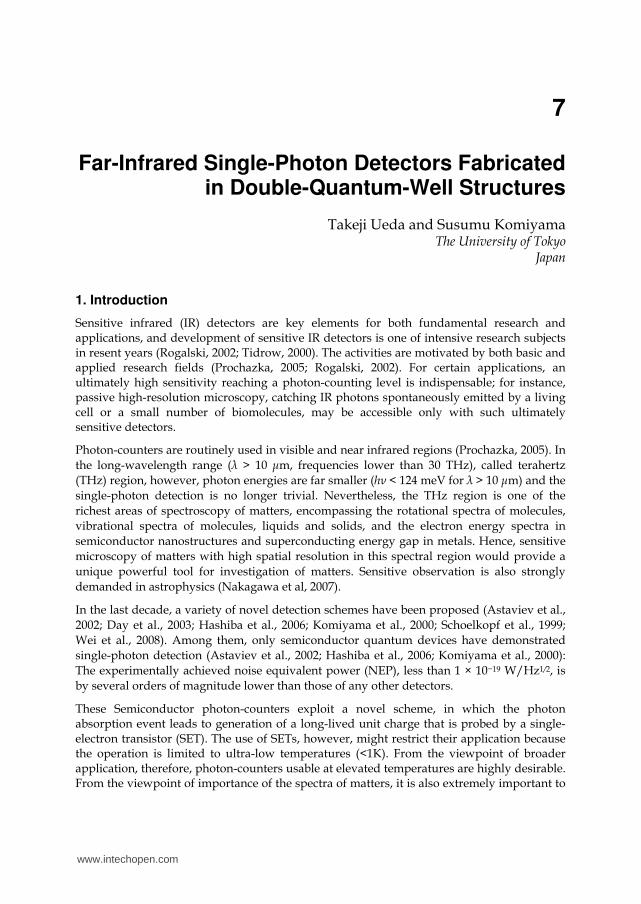
Fig. 1. (a) Schematic representation of the charge sensitive infrared phototransistor (CSIP) as
a phpto-active field-effect transistor. (b) The energy diagram of double-quantum-well
system. (c) Crystal strucuture for detection wavelength of 15 ┤m.
The upper QW is so designed that the energy spacing between the ground subband and the first excited subband is ⦆E =84 meV (for detection wavelength of ┣=15 ┤m). When radiation with photon energy of ⦆E is incident on the isolated QW, electrons are excited to the first
www.intechopen.com
Far-Infrared Single-Photon Detectors Fabricated in Double-Quantum-Well Structures
147
excited subband, where the thin tunnel barrier layer stands as schematically depicted in Fig. 1 (b). The electrons, having tunneled out of the QW, fall down the electrostatic potential slope in the graded barrier layer until they eventually reach the 2DEG channel to be absorbed there. This causes isolated QW island to be positively charged. Through capacitive coupling, the pile-up positive charge in the isolated island increases the electron density of the lower 2DEG channel leading to an increase in conductance.
The crystals are grown by molecular-beam epitaxy (MBE). The crystal structure is shown in Fig. 1 (c). Undoped GaAs (~400 nm) and 10 periods of an Al0.3Ga0.7As (20 nm)/GaAs (2 nm) superlattice were first grown on the semi-insulating substrate. Then, a 1x1024 m-3 Si doped Al0:3Ga0:7As layer (10 nm) and an Al0.3Ga0:7As spacer layer (30 nm) were grown as a remote-doping layer to supply electrons to the successively grown undoped GaAs layer (20 nm), which serves as the lower QW in the DQW system. The 150-nm thick compositionally graded AlxGa1-xAs barrier (GB) and a 2-nm thick tunnel barrier (TB) are grown as the isolation barrier between the lower and upper QWs. Here, the growth was suspended between the GB and TB to change the Al beam. The GaAs layer as the upper QW was successively grown. Finally, an Al0:3Ga0:7As spacer layer and an Al0.3Ga0.7As uniform Si doping layer (1x1024 m-3, 40 nm) were grown to supply electrons to the upper QW. The surface is covered with a 10-nm-thick GaAs cap layer. The superlattice barrier below the lower QW improves the roughness of the GaAs/AlGaAs interface. The detection wavelength is controlled by changing the design width of upper QW (Ueda et al., 2011).
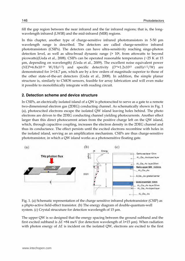
Fig. 2. (a) Schematic representation of QWs and ohmic contacts. The upper QW is electrically isolated by negative biasing of surface gates. (b) A microscope image of the device with a 16x4 ┤m2 isolated island formed by the upper QW.
As shown in Fig. 2, the device consists of a wet-etched DQW mesa, alloyed AuGeNi ohmic contacts, Au/Ti Schottky gates (the isolation gate, IG, and reset gate, RG), and Au/Ti photo-coupler (antenna). The device is fabricated with standard electron-beam lithography technique. The 2DEG layer in the both of the QWs are normally connected by ohmic contacts, and can be electrically isolated by biasing metal isolation gates. The active areas of devices are freely defined in lithography. The coupler is used to cause intersubband transition by generating electric filed normal to the plane of the QW against the normally incident radiation. It should be mentioned that the simple planar structure of CSIPs is
www.intechopen.com
Photodetectors
148
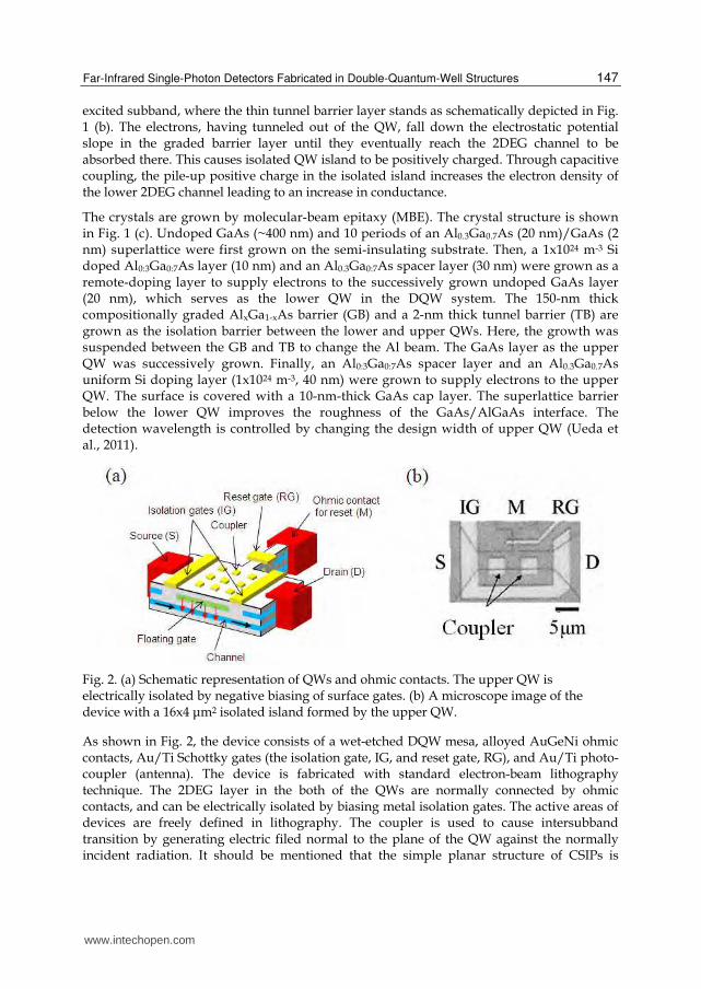
feasible for array fabrication (fabricated example is shown in Fig. 3). The FET structure would have an advantage of future monolithic integration with reading circuits.
Fig. 3. 20x 20 CSIP focal plane array
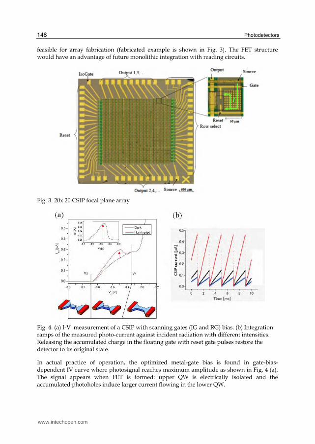
Fig. 4. (a) I-V measurement of a CSIP with scanning gates (IG and RG) bias. (b) Integration ramps of the measured photo-current against incident radiation with different intensities. Releasing the accumulated charge in the floating gate with reset gate pulses restore the detector to its original state.
In actual practice of operation, the optimized metal-gate bias is found in gate-bias-dependent IV curve where photosignal reaches maximum amplitude as shown in Fig. 4 (a). The signal appears when FET is formed: upper QW is electrically isolated and the accumulated photoholes induce larger current flowing in the lower QW.
www.intechopen.com
Far-Infrared Single-Photon Detectors Fabricated in Double-Quantum-Well Structures
149
As in Fig. 4 (b), to avoid the saturation of the signal, the accumulated charge is released to the reservoir by applying a brief positive pulse (e.g., +0.3V, 1 ┤s) to the RG, and the CSIP is reset to the original highly sensitive state (An et al., 2007). Conventional photoconductive detectors yield a certain amplitude of photocurrent that is proportional to the incident radiation intensity. The scheme of CSIPs is different: The source-drain current continues to increase with time under steady illumination, where the speed at which the current increases, α=⦆I/⦆t, is proportional to the incident radiation intensity.
This photoresponse can be interpreted by increase of electron density in lower QW induced by capacitively coupled photoholes stored in the isolated upper QW. The unit increment of current Ie induced by one photohole in the isolated upper QW (area of L × W) is given by:
2SD
e
e VI
L
(1)
where e is the unit charge, ┤ the electron mobility of lower QW, VSD the souce-drain (SD) voltage, L the length of constricted channel. For example, unit increment Ie = 3 pA is given for ┤ = 1 m2/Vs, VSD = 10 mV and L = 16 ┤m. The signal Ie persists as long as a photohole stays in upper QW. By setting the lifetime τ = 1 s, the amplification factor, or photoconductive gain, is given as G = τIe/e = 1.8 × 10⁷. This value is comparable to that of
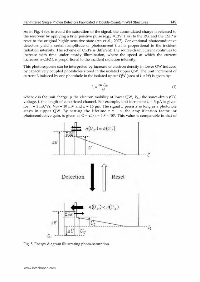
Fig. 5. Energy diagram illustrating photo-saturation.
www.intechopen.com
Photodetectors
150
photomultiplier tubes. The increase of the current is proportional to the number of accumulated photoholes p:
⦆I = pIe (2)
Under steady illumination, p is a linearly increasing function of time if the lifetime of photoholes is longer than the relevant time of integration. The number of photoholes, of course, does not increase infinitely, but reach a saturated value. The saturation is caused by balance between generation and recombination speeds of photoholes which change with deformation of the potential profile due to accumulating positive charges in upper QW, as shown in Fig. 5. The potential drop is given by ∆U = pe2d/┝LW, where d = 150 nm is the distance between upper and lower QWs, ┝ = 12 × (8.85 × 10−12) F/m is the electric permittivity of GaAs. The number of photoholes is described by the rate equation:
dp p
dt (3)
where ┟ is quantum efficiency, Φ is the incident photon flux (photons/s), and τ is the lifetime of photoholes. The first and second term in the right-hand side of Eq. 3 refer to the generation and recombination speed of photoholes, respectively.
3. All-cryogenic spectrometer
It is not trivial to accurately characterize ultrasensitive detectors in far infrared region. In usual setup, a monochromator system is placed at room temperature. Then, in case of ultrasensitive detection in far-IR and THz region, the measurements suffer from the thermal background blackbody radiation (BBR) at 300K that can be much stronger than the light guided from the external source. This caused a serious problem for the study of extremely sensitive CSIPs, the intrinsic characteristics of which may be significantly affected by relatively weak background radiation. It was also difficult to determine accurate excitation spectrum.
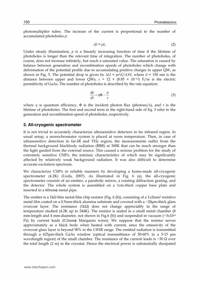
We characterize CSIPs in reliable manners by developing a home-made all-cryogenic spectrometer (4.2K) (Ueda, 2007). As illustrated in Fig. 6 (a), the all-cryogenic spectrometer consists of an emitter, a parabolic mirror, a rotating diffraction grating, and the detector. The whole system is assembled on a 1cm-thick copper base plate and
inserted in a 60mm metal pipe.
The emitter is a 1kΩ thin metal-film chip resistor (Fig. 6 (b)), consisting of a 1x2mm2 resistive metal film coated on a 0.5mm-thick alumina substrate and covered with a ~20┤m-thick glass overcoat layer. The resistance (1kΩ) does not change appreciably in the range of temperature studied (4.2K up to 244K). The resistor is sealed in a small metal chamber (8 mm-length and 4 mm-diameter, not shown in Fig.6 (b)) and suspended in vacuum (~3x10⁻⁴
Pa) by current leads (0.2mm Manganin wires). We suppose that the resistor serves approximately as a black body when heated with current, since the emissivity of the overcoat glass layer is beyond 90% in the LWIR range. The emitted radiation is transmitted through a 625┤m-thick GaAs window (optical transmittance of 50-60% in a 5-15 ┤m wavelength region) of the small chamber. The resistance of the current leads is ~30 Ω over the total length (2 m) in the cryostat. Hence the electrical power is substantially dissipated
www.intechopen.com
Far-Infrared Single-Photon Detectors Fabricated in Double-Quantum-Well Structures
151
by the chip resistor. The emitter temperature, Temitter, is monitored with a thermocouple, Chromel-Au/Fe (0.07 %) glued to the backside of the resistor (Fig.6 (b)). The values of Temitter will be shown as a function of the input electrical power Pin in the inset of Fig.9 (b).
Fig. 6. (a) All cryogenic spectrometer; schematic representation and a photograph. (b) A 1kΩ thin metal film chip resistor serving as a black-body radiator. The emitter is packaged in a small vacuum metal chanber with a GaAs window.
The parabolic mirror collimates broadband BBR from the emitter and directs it to the diffraction grating, which will be described in the next paragraph. The angle of diffraction grating is controlled mechanically from the outside of the cryostat. The radiation diffracted at the grating is guided to the detector. The detector is installed in a small copper box with a 4 mm and 20 mm-long metal pipe at the entrance. The inner wall of the entrance pipe is screw patterned so as to prevent stray lights from entering the detector box.
A home-made diffraction grating is used. Commercially available diffraction gratings are usually composed of materials of different thermal expansion coefficients, like an epoxy substrate coated with aluminum films. They are hence unreliable for the use at cryogenic temperatures. We fabricated a diffraction grating using a GaAs crystal. A GaAs crystal surface was patterned into 7.5┤m-wide and 7.5┤m-deep trenches at 15 ┤m-period via mesa etching with a solution of H2PO4 : H2O2 : H2O = 4 : 1 : 40 (etching rate: 40 nm/min) at 25 oC. The etching was made for 4.5 hours. The slow rate and the long time of etching were chosen so as to round the grove edges through under-etching the resist mask. The rounding of grove edges was necessary for obtaining a reasonable amplitude for the 1st-order diffraction by reducing the 0th-order diffraction (specular reflection). Finally the trenched GaAs surface was coated with a 20nm-Ti/300nm-Au layer via vacuum evaporation.
The whole spectrometer system is immersed in liquid helium (T=4.2K). The 300K BBR from the warm part of the cryostat is blocked by placing copper plates at a 10 cm-interval inside the metal pipe. The emitter chamber is made vacuum by pumping through a thin, 4-mm
diameter, metal pipe. The pipe is narrowed to 2mm at the entry to the chamber and bended at two places for minimizing the 300K-BBR entering through the vacuum pipe.
The wavelength resolution of the present optical setup was evaluated to be ⦆┣g=1.0 ┤m (full width at half maximum, FWHM) by using a Fourier Transform Infrared Spectroscopy (FTIR) system.
www.intechopen.com
Photodetectors
152
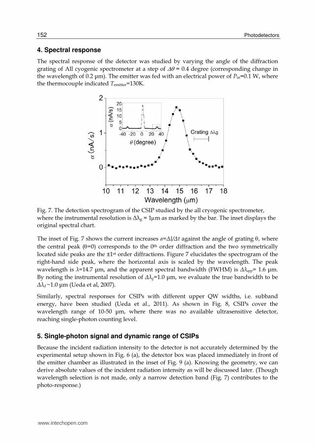
4. Spectral response
The spectral response of the detector was studied by varying the angle of the diffraction
grating of All cyogenic spectrometer at a step of = 0.4 degree (corresponding change in the wavelength of 0.2 ┤m). The emitter was fed with an electrical power of Pin=0.1 W, where the thermocouple indicated Temitter=130K.
Fig. 7. The detection spectrogram of the CSIP studied by the all cryogenic spectrometer,
where the instrumental resolution is Δ┣g = 1m as marked by the bar. The inset displays the original spectral chart.
The inset of Fig. 7 shows the current increases α=⦆I/⦆t against the angle of grating , where
the central peak (=0) corresponds to the 0th order diffraction and the two symmetrically
located side peaks are the ±1st order diffractions. Figure 7 elucidates the spectrogram of the
right-hand side peak, where the horizontal axis is scaled by the wavelength. The peak
wavelength is ┣=14.7 ┤m, and the apparent spectral bandwidth (FWHM) is ⦆┣app= 1.6 ┤m.
By noting the instrumental resolution of ⦆┣g=1.0 ┤m, we evaluate the true bandwidth to be
⦆┣d ~1.0 ┤m (Ueda et al, 2007).
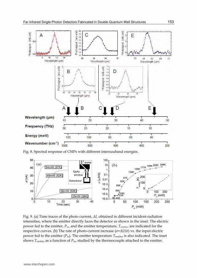
Similarly, spectral responses for CSIPs with different upper QW widths, i.e. subband
energy, have been studied (Ueda et al., 2011). As shown in Fig. 8, CSIPs cover the
wavelength range of 10-50 ┤m, where there was no available ultrasensitive detector,
reaching single-photon counting level.
5. Single-photon signal and dynamic range of CSIPs
Because the incident radiation intensity to the detector is not accurately determined by the
experimental setup shown in Fig. 6 (a), the detector box was placed immediately in front of
the emitter chamber as illustrated in the inset of Fig. 9 (a). Knowing the geometry, we can
derive absolute values of the incident radiation intensity as will be discussed later. (Though
wavelength selection is not made, only a narrow detection band (Fig. 7) contributes to the
photo-response.)
www.intechopen.com
Far-Infrared Single-Photon Detectors Fabricated in Double-Quantum-Well Structures
153
Fig. 8. Spectral response of CSIPs with different intersuuband energies.
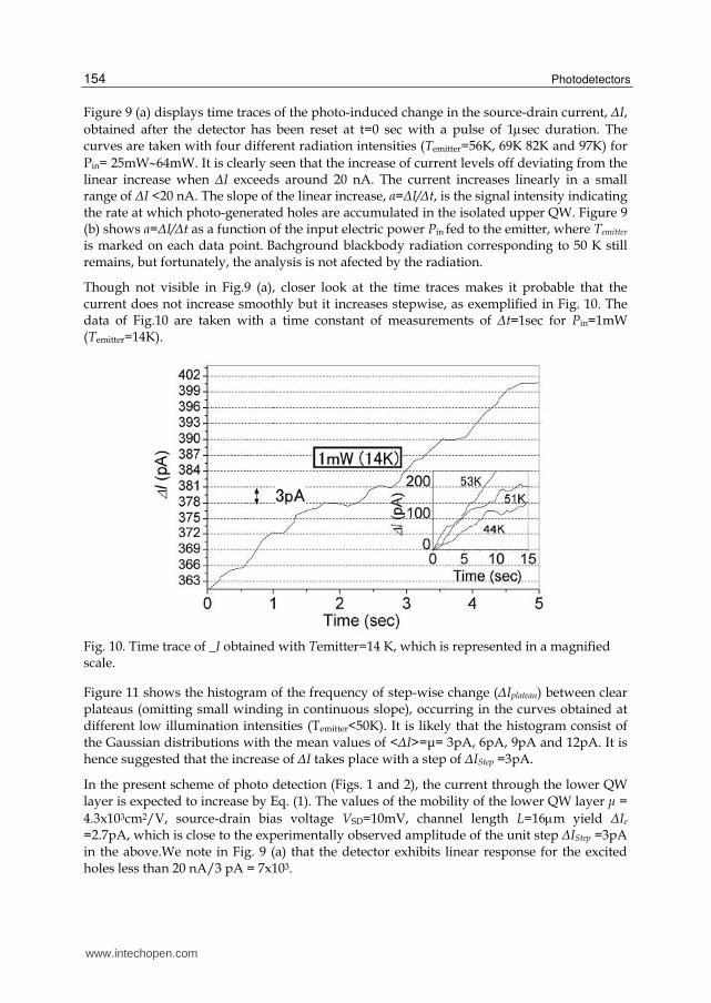
Fig. 9. (a) Time traces of the photo current, ⦆I, obtained in different incident-radiation
intensities, where the emitter directly faces the detector as shown in the inset. The electric
power fed to the emitter, Pin, and the emitter temperature, Temitter, are indicated for the
respective curves. (b) The rate of photo-current increase (α=⦆I/⦆t) vs. the input electric
power fed to the emitter (Pin). The emitter temperature Temitter is also indicated. The inset
shows Temitter as a function of Pin, studied by the thermocouple attached to the emitter.
www.intechopen.com
Photodetectors
154
Figure 9 (a) displays time traces of the photo-induced change in the source-drain current, ⦆I,
obtained after the detector has been reset at t=0 sec with a pulse of 1sec duration. The curves are taken with four different radiation intensities (Temitter=56K, 69K 82K and 97K) for
Pin= 25mW64mW. It is clearly seen that the increase of current levels off deviating from the linear increase when ⦆I exceeds around 20 nA. The current increases linearly in a small range of ⦆I <20 nA. The slope of the linear increase, α=⦆I/⦆t, is the signal intensity indicating the rate at which photo-generated holes are accumulated in the isolated upper QW. Figure 9 (b) shows α=⦆I/⦆t as a function of the input electric power Pin fed to the emitter, where Temitter is marked on each data point. Bachground blackbody radiation corresponding to 50 K still remains, but fortunately, the analysis is not afected by the radiation.
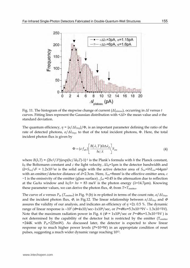
Though not visible in Fig.9 (a), closer look at the time traces makes it probable that the current does not increase smoothly but it increases stepwise, as exemplified in Fig. 10. The data of Fig.10 are taken with a time constant of measurements of ⦆t=1sec for Pin=1mW (Temitter=14K).
Fig. 10. Time trace of _I obtained with Temitter=14 K, which is represented in a magnified scale.
Figure 11 shows the histogram of the frequency of step-wise change (⦆Iplateau) between clear plateaus (omitting small winding in continuous slope), occurring in the curves obtained at different low illumination intensities (Temitter<50K). It is likely that the histogram consist of the Gaussian distributions with the mean values of <⦆I>=┤= 3pA, 6pA, 9pA and 12pA. It is hence suggested that the increase of ⦆I takes place with a step of ⦆IStep =3pA.
In the present scheme of photo detection (Figs. 1 and 2), the current through the lower QW layer is expected to increase by Eq. (1). The values of the mobility of the lower QW layer ┤ =
4.3x103cm2/V, source-drain bias voltage VSD=10mV, channel length L=16m yield ⦆Ie =2.7pA, which is close to the experimentally observed amplitude of the unit step ⦆IStep =3pA in the above.We note in Fig. 9 (a) that the detector exhibits linear response for the excited holes less than 20 nA/3 pA = 7x10³.
www.intechopen.com
Far-Infrared Single-Photon Detectors Fabricated in Double-Quantum-Well Structures
155
Fig. 11. The histogram of the stepwise change of current (⦆Iplateau), occurring in ⦆I versus t curves. Fitting lines represent the Gaussian distribution with <⦆I> the mean value and ┫ the standard deviation.
The quantum efficiency, ┟ = {α/⦆IStep}/, is an important parameter defining the ratio of the
rate of detected photons, α/⦆IStep, to that of the total incident photons, . Here, the total
incident photon flux is given by
,( ) d
att em
B Tf S
hc
(4)
where B(┣,T) = (2hc2/┣5){exp(hc/┣kBT)-1}-1 is the Plank’s formula with h the Planck constant,
kB the Boltzmann constant and c the light velocity, ⦆┣d=1┤m is the detector bandwidth and
Ω=Siso/d2 = 1.2x10⁻⁷sr is the solid angle with the active detector area of Siso=WLiso=64┤m2
with an emitter/detector distance of d=2.3cm. Here, Sem=8mm2 is the effective emitter area, ┝ ~1 is the emissivity of the emitter (glass surface) , fatt =0.45 is the attenuation due to reflection
at the GaAs window and hc/┣= h┥ = 83 meV is the photon energy (┣=14.7┤m). Knowing
these parameter values, we can derive the photon flux, , from T=Temitter.
The curve of α versus Pin (Temitter) in Fig. 9 (b) is re-plotted in terms of the count rate, α/⦆IStep,
and the incident photon flux, , in Fig.12. The linear relationship between α/⦆IStep and
assures the validity of our analysis, and indicates an efficiency of ┟ =2 0.5 %. The dynamic
range of linear response is 107 (=4x10/sec1x108/sec, or P=h┥=5.3x10⁻¹⁹W 1.3x10⁻¹²W).
Note that the maximum radiation power in Fig. 6 ( = 1x10⁸/sec or P=h┥=1.3x10⁻¹²W ) is
not determined by the capability of the detector but is restricted by the emitter (Temitter
=244K with Pin=225mW). As discussed later, the detector is expected to show linear
response up to much higher power levels (P=10-6W) in an appropriate condition of reset
pulses, suggesting a much wider dynamic range reaching 1013.
www.intechopen.com
Photodetectors
156
Fig. 12. Count rate of the photosignal vs. incident photon flux . Photon fluxes of =102
photons/sec corresponds to Pin = h┥ = 1.3x10⁻¹⁸W.
6. Figures of merit
The current responsivity of the detector, R=⦆I/(h┥Φ), is the photocurrent amplitude ⦆I divided by the incident radiation power. In the CSIP, ⦆I=α⦆tI is proportional to the integration time, ⦆tI, which can be arbitrarily chosen. If we take a typical reset interval, in a
range of ⦆tI=10msec1sec, we derive R=┟(⦆IStep/h┥)⦆tI = (4x1044x106) A/W by noting
┟={α/⦆IStep}/ with ⦆IStep =3pA and ┟=0.02. The responsivity is thus by many orders of magnitude larger than that of well known QWIPs, for which R is typically ~0.5A/W (Levine, 1993; Yao, 2000). We can also write the responsivity as R=┟(e/h┥)g by using the “photoconductive gain” g, which refers to the effective number of electrons generated by a single photon. We mention that the large value of R comes from the extremely high
photoconductive gain, g=(⦆IStep/e) ⦆tI = 1x1051x107 , in the CSIP.
Noise equivalent power (NEP) is defined by
P
NEPSNR f
(5)
where P is the power of incident radiation, SNR is the signal to noise ratio, and ⦆f=1/(2⦆t) is the frequency bandwidth of measurements with ⦆t the averaging time. We evaluate Eq.(5) by taking three curves of ⦆I versus t shown in the inset of Fig.7 as an example. These curves are taken for Temitter=44K (Pin= 2.8aW), 51K (4.5aW) and 55K (5.0aW). Considering the time
constant ┬ =1sec of measurements, we evaluate the noise from 2( ) , where is the
average slope (count rate) of each curve for a long time (>15 sec) and α=⦆I/⦆t is the slope at each point over ⦆t=1sec. For each curve, we derive SNR = 2.1, 1.9 and 2.2 for ⦆t = 1sec and obtain NEP = 1.9x10⁻¹⁸, 3.4x10⁻¹⁸ and 3.3x10⁻¹⁸ W/Hz1/2.
It is interesting if the noise in the present measurements arises from detector specific electrical noise or is ascribed to the photon noise. If the detector noise is ignored, random
www.intechopen.com
Far-Infrared Single-Photon Detectors Fabricated in Double-Quantum-Well Structures
157
events of photon arrival give rise to the photon noise, like the shot noise in the electron current. On the average, N⦆t photons are counted over integration time of ⦆t when the
photon count rate is N=┟=α/⦆IStep. Since the standard deviation from the average is given by (N⦆t)1/2 in the Poisson distribution, SNR of an ideal detector (free from any detector-specific noises) is (N⦆t)1/2 . It follows that NEP is given by (Knuse et al., 1962)
2 2
BLIP
NNEP h h (6)
in the condition when the noise is dominated by the photon noise; i.e., in the background limited performance (BLIP). We have NEPBLIP = 1.9x10⁻¹⁸, 2.5 x10⁻¹⁸ and 2.6 x10⁻¹⁸ W/Hz1/2, respectively, for the three conditions (N=4.2, 6.7 and 7.4) of the data in the inset of Fig.10. The fact that these values are close to the NEP values derived from Eq.(5) indicates that the fluctuation in the present measurements comes from the randomness in the photon arrival events and that the detector-specific noise is indiscernibly small.
The true NEP is obtained by replacing N in Eq.(6) by the dark count rate ポ, (Brule Technologies, Inc., 1980)
2
NEP h (7)
In the present spectrometer, weak background radiation makes hinders direct determination of ポ because of background blackbody corresponding at 50 K. In another optical system, we studied the detector in the complete dark condition, and obtained ポ=0.5 sec-1, which yields NEP=6.8 x10⁻¹⁹ W/Hz1/2.
The fact hat the noise in the present measurements arises from the photon noise is also
supported by the inter-step interval histograms. A time trace of I for Pin=1mW was studied
for 700 seconds in the present spectrometer (partially shown in Fig. 10). The local slope of
the curve, α(t)= I/ t, was numerically calculated at each time point t of the curve, where the
value is averaged over 1sec at each point. Figure 13 (a) represents the frequency of different
slopes as a function of the steps per seconds or α(t)/⦆IStep with ⦆IStep =3pA. In the trace of I,
upward stepwise change as well as downward change are recognized, which were
separately analyzed in Fig.13 (b) (Gain) and (c) (Loss). As expected for single-photon
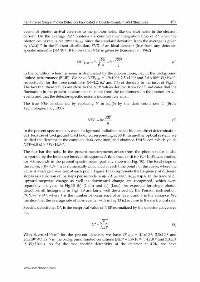
detection, all histograms in Figs. 10 are fairly well described by the Poisson distribution,
f(k,N)=e- k/k!, where k is the number of occurrence of an event and is the variance. We
mention that the average rate of Loss events =0.5 in Fig.13 (c) is close to the dark count rate.
Specific detectivity, D*, is the reciprocal value of NEP normalized by the detector active area Siso,
* isoSD
NEP (8)
With Siso=64x10-8cm2 for the present detector, we have D*BLIP = 4.1x10¹⁴, 2.3x10¹⁴ and 2.5x10¹⁴W/Hz1/2 in the background limited conditions (NEP = 1.9x10⁻¹⁸, 3.4x10⁻¹⁸ and 3.3x10-
18 W/Hz1/2). As for the true specific detectivity of the detector at 4.2K, we have
www.intechopen.com
Photodetectors
158
D*1.2x1015cmHz1/2/W from NEP6.8x10-19W/Hz1/2. CSIPs are thus highly sensitive detectors with values of D* much higher than those of conventional detectors like QWIPs (D*=1010-1013cmHz1/2/W at 4.2~80K) (Levine, 1993; Yao et al., 2000) and mercury-cadmium telluride (MCT) detectors (D*~1010cmHz1/2/W at ~80K) (Rogalski, 2002).
Fig. 13. Histogram of the photo-current I per second. The photocurrent is measured in unit of ⦆IStep =3pA so that the horizontal axis is scaled by the number of steps per second,
(I/⦆IStep)/t = α/⦆IStep. The data are derived by analyzing a time trace of I for 700 sec at Pin=1mW: (a) All events of both gain signal (generation of holes) and loss signal (loss of holes due to recombination) are included. In (b) and (c), the gain signal and the loss signal are separately shown.
The intrinsic speed of detection will be limited by the transistor operation, which may be
faster than 1 ns. In actual practice of detector operation, the detection speed may be
determined by the frequency of applicable rest pulse, which may be restricted to about 300
MHz (~3 ns interval). The maximum incident radiation power will be hence Pmax~ (7x10³
h┥/3 ns)/ ~ 2 W, which makes us to expect that the dynamic range can be expanded to 1013
by assuming the minimum detectable power to be Pmin~1x10-19W.
7. Improvement of quantum efficiency
Quantum efficiency ┟ is an important parameter for the detector. High values of ┟ (>30%)
are reported in conventional QW IR photodetectors, where photons are absorbed by more
than 30 multiple QWs. High quantum efficiency is not trivial in CSIPs, where photons are
absorbed by only one QW. In most experimental conditions of CSIP for ┣ = 12–15 ┤m, the
efficiency ┟ = ┟1┟2 is primarily determined by the coupling strength of electrons to the
incident radiation, namely, ┟ ≈ ┟1 (┟2 ≈ 1).
Recently we proposed and demonstrated efficient photo-couplers for CSIPs (┣=15 ┤m) by
exploiting surface-plasmon-polariton (SPP) resonance occurring in aperture metal sheets
coated on top of the crystal surface (Fig. 14 (a)) (Nickels et al, 2010). The SPP resonance
induces wavelength-selective strong electric confined near the surface of the metal sheets
www.intechopen.com
Far-Infrared Single-Photon Detectors Fabricated in Double-Quantum-Well Structures
159
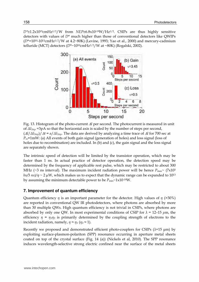
intensifying the subband transition in the QW 100 nm below the surface. The quantum
efficiency has been experimentally studied by applying different metal photocouplers as
displayed in Fig. 14 (b) and compared with simulation results in Fig. 14 (c).
Fig. 14. (a) Schematic representation of photocoupler. (b) Metal meshes studied. White and black characters indicate, respectively, the lattice period p and the experimentally derived quantum efficiency ┟. (c)Results of simulation calculation are shown for (a) cross-hole arrays and (b) square-hole arrays: from the top, normalized field intensity <Ez2>/<Ez02>, the total power transmission, and the zeroth-order transmission, against the ratio ┣GaAs /p with ┣GaAs = 4.3 ┤m.Ez is the electric field normal to the QW plane at the position of upper QW(100 nm below the surface) and Ex0 is the electric field of incident radiation. Theoretically, <Ez2>/<Ez02>,= 2 gives roughly ┟ = 7%, which agrees with the experiment
In the experiments, an efficiency of ┟ ≈ 7% has been achieved by utilizing the surface
plasmon excitation in a 2-D metal hole array (inductive metal mesh) with cross-shaped holes
lining up at a lattice period of 4 ┤m (~ wavelength in GaAs). Other coupler geometries such
as 2-D metal hole arrays with square-shaped holes, 2-D metal patch arrays (capacitive metal
mesh), and patch antennas (microstrip antennas) have yielded lower values of ┟ ≈ 1%–3%
(Ueda et al., 2008; Nickels et al, 2010). The device used for Fig. 12, for instance, utilizes a
patch antenna coupler yielding ┟ ≈ 2% (Ueda et al, 2008). Simulation suggests that ┟ ≈ 7% is
not a highest achievable value but can be improved by a factor of ~3 (┟ ≈ 20%) when a
resonant cavity is formed by the metal hole array and the n-type substrate. Values of the
current responsivity and the NEP given in the section 6 have been so far derived by
assuming ┟ = 2%. The figure-of-merits of the CSIP will be improved in accordance to ┟.
www.intechopen.com
Photodetectors
160
8. Temperature dependence of the performance
Higher temperature operation is desired for practical applications. There is in general, however, a trade-off between high sensitivity of an IR detector and operation temperature. The external constraint is that sensitive devices are saturated by strong background blackbody radiation from surrounding materials. The internal constraint is that the thermionic emission inside the device becomes equivalent to photo-emission. The former may be determined by optical setup, as well as relative intensity of signal radiation to the background. Here, we discuss the latter intrinsic constraint.
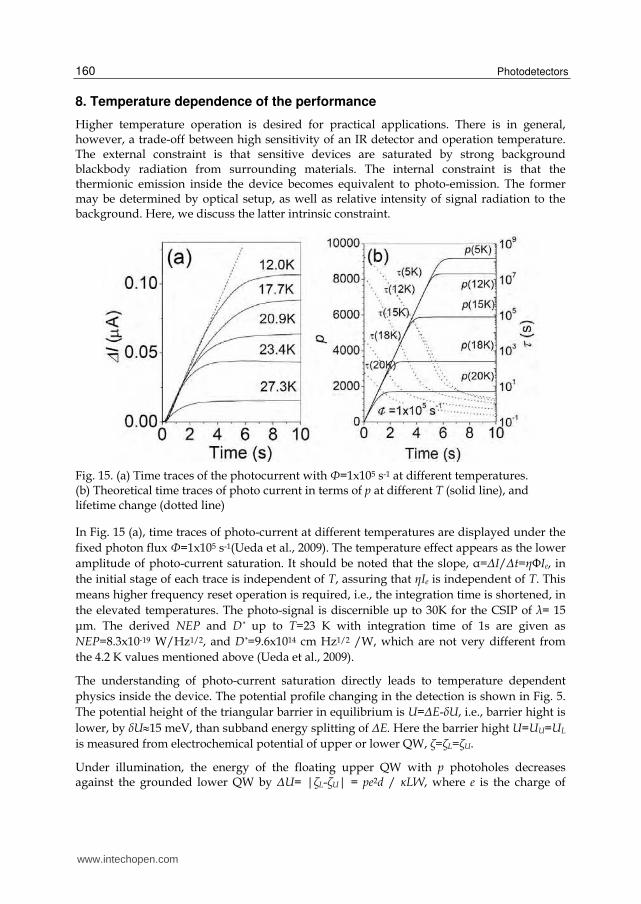
Fig. 15. (a) Time traces of the photocurrent with Φ=1x10⁵ s-1 at different temperatures. (b) Theoretical time traces of photo current in terms of p at different T (solid line), and lifetime change (dotted line)
In Fig. 15 (a), time traces of photo-current at different temperatures are displayed under the
fixed photon flux Φ=1x10⁵ s-1(Ueda et al., 2009). The temperature effect appears as the lower
amplitude of photo-current saturation. It should be noted that the slope, α=⦆I/⦆t=┟ΦIe, in
the initial stage of each trace is independent of T, assuring that ┟Ie is independent of T. This
means higher frequency reset operation is required, i.e., the integration time is shortened, in
the elevated temperatures. The photo-signal is discernible up to 30K for the CSIP of ┣= 15
┤m. The derived NEP and D* up to T=23 K with integration time of 1s are given as
NEP=8.3x10⁻¹⁹ W/Hz1/2, and D*=9.6x1014 cm Hz1/2 /W, which are not very different from
the 4.2 K values mentioned above (Ueda et al., 2009).
The understanding of photo-current saturation directly leads to temperature dependent
physics inside the device. The potential profile changing in the detection is shown in Fig. 5.
The potential height of the triangular barrier in equilibrium is U=⦆E-├U, i.e., barrier hight is
lower, by ├U15 meV, than subband energy splitting of ⦆E. Here the barrier hight U=UU=UL
is measured from electrochemical potential of upper or lower QW, ┞=┞L=┞U.
Under illumination, the energy of the floating upper QW with p photoholes decreases against the grounded lower QW by ⦆U= |┞L-┞U| = pe2d / ┢LW, where e is the charge of
www.intechopen.com
Far-Infrared Single-Photon Detectors Fabricated in Double-Quantum-Well Structures
161
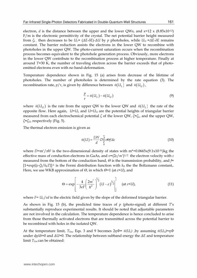
electron, d is the distance between the upper and the lower QWs, and ┢=12 x (8.85x10-12) F/m is the electronic permittivity of the crystal. The net potential barrier height measured from ┞L , then decreases to be UL= (⦆E-├E)-⦆U by p photoholes, while UU =⦆E-├E remains constant. The barrier reduction assists the electrons in the lower QW to recombine with photoholes in the upper QW. The photo-current saturation occurs when the recombination process becomes equivalent to the photohole generation process. Obviously, more electrons in the lower QW contribute to the recombination process at higher temperature. Finally at around T=30 K, the number of traveling electron across the barrier exceeds that of photo-emitted electrons even with no band-deformation.
Temperature dependence shown in Fig. 15 (a) arises from decrease of the lifetime of
photoholes. The number of photoholes is determined by the rate equation (3). The
recombination rate, p/, is given by difference between Ln U and Un U ,
L U
pn U n U (9)
where Un U is the rate from the upper QW to the lower QW and Ln U the rate of the
opposite flow. Here again, U=UL and U=UU are the potential heights of triangular barrier
measured from each electrochemical potential ┞ of the lower QW, ┞=┞L, and the upper QW,
┞=┞U, respectively (Fig. 5).
The thermal electron emission is given as
0
LWn U D v f d
d (10)
where D=m*/πħ2 is the two-dimensional density of states with m*=0.0665x(9.1x10-31)kg the
effective mass of conduction electrons in GaAs, and v=(2┝/m*)1/2 the electron velocity with ┝ measured from the bottom of the conduction band, Θ is the transmission probability, and f=
[1+exp{(┝-┞)/kBT}]-1 is the Fermi distribution function with kB the the Boltzmann constant,.
Here, we use WKB approximation of Θ, in which Θ=1 (at ┝>U), and
1* 2 3
22
4 2exp
3
mU
eF (at ┝<U), (11)
where F= UL/ed is the electric field given by the slope of the deformed triangular barrier.
As shown in Fig. 15 (b), the predicted time traces of p (photo-signal) at different T’s
substantially reproduce experimental results. It should be noted that adjustable parameters
are not involved in the calculation. The temperature dependence is hence concluded to arise
from those thermally activated electrons that are transmitted across the potential barrier to
be recombined with holes in the isolated QW.
At the temperature limit, Tlim, Eqs. 3 and 9 becomes 2┟Φ= ń(UL) ,by assuming ń(UU)≈┟Φ
under dp/dt=0 and ⦆U=0. The relationship between subband energy the ⦆E and temperature
limit Tlim can be obtained:
www.intechopen.com
Photodetectors
162
lim lim
lim
2lnB
B
dE E k T T
LWDvk T
(12)
where v=(2EF/m*)1/2 is Fermi velocity. Here, integration is made only for E > U with Θ=1
and f exp(-E/kBT), i.e., only thermionic emission is considered. Since contribution of Tlim in the logarithm is not significant, the temperature limit shows almost linear dependence on the subband energy with quasi-constant ┛ >0. For the ┣=15 ┤m, the parameter values yields Tlim =29 K, which is close to the experimentally observed limit temperature.
9. Conclusion
We have developed the novel ultrasensitive detectors, named charge-sensisve infrared phototransistors (CSIPs). We demonstrated the single-photon detection in the wavelength range of 10 – 50 ┤m for the first time. The accurately determined specific detectivity as D*=9.6x1014 cm Hz1/2/W for ┣=14.7 ┤m is by a few orders of magnitude higher than those of other conventional detectors. In addition, the planar FET structure of CSIPs is feasible for developing large scale array including monolithic integration with readout circuit. The quantum efficiency is improved up to 7% by using the surface-plasmon polariton couplers. The detectors can keep the sensitivity up to T=23 K for ┣=15 ┤m, and the temperature dependence of the detector performance is reasonably interpreted by a simple theoretical model. We developed CSIPs for several wavelengths in 10-50┤m, covering attractive spectral range for passive observation of spontaneous emission from RT object. Recently CSIPs have been applied to the construction of a highly sensitive passive microscope (Kajihara et al., 2009; 2010; 2011).
10. Acknowledgment
This work was supported by CREST and SORST projects of Japan Science and Technology Agency (JST). The reserach work has been carrierd with number of collaborators. Particularly T. Ueda would like to thank Z. An, P. Nickels, N. Nagai, Z. Wang and S. Matsuda for their valuable contributions.
11. References
An, Z., Ueda, T., Komiyama, S. & Hirakawa, K. (2007). Reset Operation of Qwantum-Well Infrared Phototransistors, IEEE Transaction on Electron devices, Vol. 75, pp. 1776-1780, ISSN 0018-9383
Andersson, J. & Lundqvist, L. (1991). Near-Unity Quantum Efficiency of AlGaAs/GaAs Quantum Well Infrared Detectors Using a Waveguide with a Doubly Periodic Grating Coupler, Applied Physics Letters, Vol. 59, pp. 857 1-3, ISSN 0003-6951
Astaviev. O., Komiyama, S., Kutsuwa T., Antonov, V. & Kawaguchi, Y. (2002). Single-Photon Detector in the Microwave range, Applied Physics Letters, Vol. 80, pp. 4250 1-3, ISSN 0003-6951
Burle Technologies, Inc. (1980). Photomultiplier Handbook – Theory Design Application, Lancaster, PA
Cwik, T. & Yeh, C. (1999). Higjly Sensitive Quantum Well Infrared Photodetectors, Journal of Applied Physics, Vol. 86, pp. 2779 1-6, ISSN 0021-8979
www.intechopen.com
Far-Infrared Single-Photon Detectors Fabricated in Double-Quantum-Well Structures
163
Day, P., LeDuc, L., Mazin, B., Vayonakis, A. & Zmuidzinas, J. (2003). A Broadband Superconducting Detector Suitable for Use in Large Arrays, Nature, Vol. 425, pp. 817-821, ISSN 0028-0836
Hashiba, H., Antonov, V., Kulik, L., Tzalenchuk, A., Kleindschmid, P., Giblin, S. & Komiyama, S. (2006). Isolated quantum dot in application to terahertz photon counting, Physical Review B, Vol. 73, pp. 081310 1-4, ISSN 0613-1829
Ikushma, K., Yoshimura, Y., Hasegawa, H., Komiyama, S., Ueda, T. & Hirakawa, K. (2006). Photon-Counting Microscopy of Terahertz Radiation, Applied Physics Letters, Vol. 88, pp. 152110 1-3, ISSN 0003-6951
Komiyama, S., Astaviev. O., Antonov, V., Kutsuwa T. & Hirai, H. (2000). A Single-Photon Detector in the Far-Infrared Range, Nature, Vol. 403, pp. 405-407, ISSN 0028-0836
Kajihara, Y., Komiyama, S., Nickels, P. & Ueda, T. (2009). A Passive Long-Wavelength infrared Microscope with a Highly sensitive phototransistor, Review of Scientific Instruments, Vol. 80, pp. 063702 1-4, ISSN 0034-6748
Kajihara, Y., Kosaka, K., Komiyama, S., Kutsuwa T. & Hirai, H. (2010). A Sensitive Near-Field Microscope for Thermal Radiation, Review of Scientific Instruments, Vol. 81, pp. 033706 1-4, ISSN 0034-6748
Kajihara, Y., Kosaka, K.& Komiyama, S. (2011). Thermally excited Near-Field Radiation and Far-Field Interfarence, Optics Express, Vol. 19, pp. 7695-7704, ISSN 1094-4087
Knuse, P., McGlauchlin, L. & McQuistan, R. (1962). Elements of Infrared Technology, Wiley, ISBN 978-047-1508-86-1, New York
Levine, B. (1993). Qwantum-Well Infrared Photodetectors, Journal of Applied Physics, Vol. 74, pp. R1-81, ISSN 0021-8979
Nakagawa, T. & Murakami, H. (2007). Mid- and far-infrared astoronomy mission SPICA, Advances in Space Research, Vol. 40, pp. 679-683, ISSN 0273-1177
Prochazka, I. (2005). Semiconducting Single Photon Detectors: The State of the Art, Physica Status Solidi (c), Vol. 2, pp. 1524-1532, ISSN 1610-1634
Rogalski, A. & Chrzanowski, K. (2002). Infrared Devices and Techniques, Opt-Electrics Review, Vol. 10, pp. 111-136, ISSN 1230-3402
Schoelkopf, R., Moseley, S., Stahle, C., Wahlgren, P. & Delsing, P. (1999). A concept for a submillimeter-wave single-photon counter, IEEE Transactions on Applied Superconductivity, Vol. 9, pp. 2935-2939, ISSN 1051-8223
Tidrow, M. (2000). Device Physics and State-of-the-art of Quantum Well Infrared Photodetectors and Arrays, Materials Science and Engineering: B, Vol. 74, pp. 45-51, ISSN 0921-5107
Ueda, T., An, Z., Hirakawa, K. & Komiyama, S. (2008). Charge-Sensitive Infrared Phototransistors: Characterization by an All-Cryogenic Spectrometer, Journal of Applied Physics, Vol. 103, pp. 093109 1-7, ISSN 0021-8979
Ueda, T., An, Z., Hirakawa, K., Nagai, N. & Komiyama, S. (2009). Temperature Dependence of the Performance of Charge-Sensitive Infrared Phototransistors, Journal of Applied Physics, Vol. 105, pp. 064517 1-8, ISSN 0021-8979
Ueda, T., Soh, Y., Nagai, N., Komiyama, S. & Kubota, H (2011). Charge-Sensitive Infrared Phototransistors Developped in the Wavelength Range of 10-50┤m Japanese Journal of Applied Physics, Vol. 50, pp. 020208 1-3, ISSN 0021-4922
www.intechopen.com

Photodetectors
164
Wei, J., Olaya, D., Karasik, B., Pereverzev, S., Sergeev, V. & Gershenson, M. (2008). Ultrasensitive hot-electron nanobolometer for Terahertz Astrophysics, Nature Nanotechnology, Vol. 3, pp. 495-500, ISSN 1748-3387
Yao, J., Tsui, D. & Choi, K. (2000). Noise characteristics of quantum-well infrared photodetectors at low temperatures, Applied Physics Letters, Vol. 76, pp. 206 1-3, ISSN 0003-6951
Nickels, P., Matsuda, S., Ueda, T., An, Z. & Komiyama, S. (2010). Metal Hole Arrays as a Resonant Photo-Coupler for Charge-Sensitive Infrared Phototransistors, IEEE journal of Quantum Electronics, Vol.46, pp. 384-3906, ISSN 0018-9197
www.intechopen.com

PhotodetectorsEdited by Dr. Sanka Gateva
ISBN 978-953-51-0358-5Hard cover, 460 pagesPublisher InTechPublished online 23, March, 2012Published in print edition March, 2012
InTech EuropeUniversity Campus STeP Ri Slavka Krautzeka 83/A 51000 Rijeka, Croatia Phone: +385 (51) 770 447 Fax: +385 (51) 686 166www.intechopen.com
InTech ChinaUnit 405, Office Block, Hotel Equatorial Shanghai No.65, Yan An Road (West), Shanghai, 200040, China
Phone: +86-21-62489820 Fax: +86-21-62489821
In this book some recent advances in development of photodetectors and photodetection systems for specificapplications are included. In the first section of the book nine different types of photodetectors and theircharacteristics are presented. Next, some theoretical aspects and simulations are discussed. The last eightchapters are devoted to the development of photodetection systems for imaging, particle size analysis,transfers of time, measurement of vibrations, magnetic field, polarization of light, and particle energy. Thebook is addressed to students, engineers, and researchers working in the field of photonics and advancedtechnologies.
How to referenceIn order to correctly reference this scholarly work, feel free to copy and paste the following:
Takeji Ueda and Susumu Komiyama (2012). Far-Infrared Single-Photon Detectors Fabricated in Double-Quantum-Well Structures, Photodetectors, Dr. Sanka Gateva (Ed.), ISBN: 978-953-51-0358-5, InTech,Available from: http://www.intechopen.com/books/photodetectors/far-infrared-single-photon-detectors-fabricated-in-double-quantum-well-structures

© 2012 The Author(s). Licensee IntechOpen. This is an open access articledistributed under the terms of the Creative Commons Attribution 3.0License, which permits unrestricted use, distribution, and reproduction inany medium, provided the original work is properly cited.