Family of Micro-Power Rail-to-Rail Input and Output ... · tlv2381 tlv2382 slos377a – september...
19
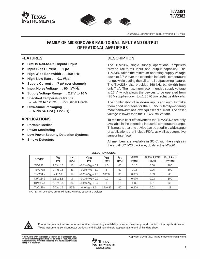
TLV2381 TLV2382 SLOS377A – SEPTEMBER 2001– REVISED JULY 2003 FAMILY OF MICROPOWER RAIL-TO-RAIL INPUT AND OUTPUT OPERATIONAL AMPLIFIERS 1 www.ti.com FEATURES BiMOS Rail-to-Rail Input/Output Input Bias Current ... 1 pA High Wide Bandwidth ... 160 kHz High Slew Rate ... 0.1 V/µs Supply Current ... 7 µA (per channel) Input Noise Voltage ... 90 nV/√Hz Supply Voltage Range ... 2.7 V to 16 V Specified Temperature Range – –40°C to 125°C ... Industrial Grade Ultra-Small Packaging – 5 Pin SOT-23 (TLV2381) APPLICATIONS Portable Medical Power Monitoring Low Power Security Detection Systems Smoke Detectors DESCRIPTION The TLV238x single supply operational amplifiers provide rail-to-rail input and output capability. The TLV238x takes the minimum operating supply voltage down to 2.7 V over the extended industrial temperature range, while adding the rail-to-rail output swing feature. The TLV238x also provides 160-kHz bandwidth from only 7 µA. The maximum recommended supply voltage is 16 V, which allows the devices to be operated from (±8 V supplies down to ±1.35 V) two rechargeable cells. The combination of rail-to-rail inputs and outputs make them good upgrades for the TLC27Lx family—offering more bandwidth at a lower quiescent current. The offset voltage is lower than the TLC27LxA variant. To maintain cost effectiveness the TLV2381/2 are only available in the extended industrial temperature range. This means that one device can be used in a wide range of applications that include PDAs as well as automotive sensor interface. All members are available in SOIC, with the singles in the small SOT-23 package, duals in the MSOP. SELECTION GUIDE DEVICE V S [V] I Q /ch [µA] V ICR [V] V IO [mV] I IB [pA] GBW [MHz] SLEW RATE [V/µs] V n , 1 kHz [nV/√Hz ] TLV238x 2.7 to 16 10 –0.2 to V S + 0.2 4.5 60 0.16 0.06 100 TLV27Lx 2.7 to 16 11 –0.2 to V S – 1.2 5 60 0.16 0.06 100 TLC27Lx 4 to 16 17 –0.2 to V S – 1.5 10/5/2 60 0.085 0.03 68 OPAx349 1.8 to 5.5 2 –0.2 to V S + 0.2 10 10 0.070 0.02 300 OPAx347 2.3 to 5.5 34 –0.2 to V S + 0.2 6 10 0.35 0.01 60 TLC225x 2.7 to 16 62.5 0 to V S – 1.5 1.5/0.85 60 0.200 0.02 19 NOTE: All dc specs are maximums while ac specs are typicals. PRODUCTION DATA information is current as of publication date. Products conform to specifications per the terms of Texas Instruments standard warranty. Production processing does not necessarily include testing of all parameters. Copyright 2001–2003 Texas Instruments Incorporated Please be aware that an important notice concerning availability, standard warranty, and use in critical applications of Texas Instruments semiconductor products and disclaimers thereto appears at the end of this data sheet.
Transcript of Family of Micro-Power Rail-to-Rail Input and Output ... · tlv2381 tlv2382 slos377a – september...
TLV2381TLV2382
SLOS377A – SEPTEMBER 2001– REVISED JULY 2003
FAMILY OF MICROPOWER RAIL-TO-RAIL INPUT AND OUTPUTOPERATIONAL AMPLIFIERS
1www.ti.com
FEATURES BiMOS Rail-to-Rail Input/Output
Input Bias Current . . . 1 pA
High Wide Bandwidth . . . 160 kHz
High Slew Rate . . . 0.1 V/µs
Supply Current . . . 7 µA (per channel)
Input Noise Voltage . . . 90 nV/√Hz
Supply Voltage Range . . . 2.7 V to 16 V
Specified Temperature Range– –40°C to 125°C . . . Industrial Grade
Ultra-Small Packaging– 5 Pin SOT-23 (TLV2381)
APPLICATIONS Portable Medical
Power Monitoring
Low Power Security Detection Systems
Smoke Detectors
DESCRIPTION
The TLV238x single supply operational amplifiersprovide rail-to-rail input and output capability. TheTLV238x takes the minimum operating supply voltagedown to 2.7 V over the extended industrial temperaturerange, while adding the rail-to-rail output swing feature.The TLV238x also provides 160-kHz bandwidth fromonly 7 µA. The maximum recommended supply voltageis 16 V, which allows the devices to be operated from(±8 V supplies down to ±1.35 V) two rechargeable cells.
The combination of rail-to-rail inputs and outputs makethem good upgrades for the TLC27Lx family—offeringmore bandwidth at a lower quiescent current. The offsetvoltage is lower than the TLC27LxA variant.
To maintain cost effectiveness the TLV2381/2 are onlyavailable in the extended industrial temperature range.This means that one device can be used in a wide rangeof applications that include PDAs as well as automotivesensor interface.
All members are available in SOIC, with the singles inthe small SOT-23 package, duals in the MSOP.
SELECTION GUIDE
DEVICEVS[V]
IQ/ch[µA]
VICR[V]
VIO[mV]
IIB[pA]
GBW[MHz]
SLEW RATE[V/µs]
Vn, 1 kHz[nV/√Hz]
TLV238x 2.7 to 16 10 –0.2 to VS + 0.2 4.5 60 0.16 0.06 100
TLV27Lx 2.7 to 16 11 –0.2 to VS – 1.2 5 60 0.16 0.06 100
TLC27Lx 4 to 16 17 –0.2 to VS – 1.5 10/5/2 60 0.085 0.03 68
OPAx349 1.8 to 5.5 2 –0.2 to VS + 0.2 10 10 0.070 0.02 300
OPAx347 2.3 to 5.5 34 –0.2 to VS + 0.2 6 10 0.35 0.01 60
TLC225x 2.7 to 16 62.5 0 to VS – 1.5 1.5/0.85 60 0.200 0.02 19
NOTE: All dc specs are maximums while ac specs are typicals.
PRODUCTION DATA information is current as of publication date.Products conform to specifications per the terms of Texas Instrumentsstandard warranty. Production processing does not necessarily includetesting of all parameters.
Copyright 2001–2003 Texas Instruments Incorporated
Please be aware that an important notice concerning availability, standard warranty, and use in critical applications ofTexas Instruments semiconductor products and disclaimers thereto appears at the end of this data sheet.
TLV2381TLV2382
SLOS377A – SEPTEMBER 2001– REVISED JULY 2003
2 www.ti.com
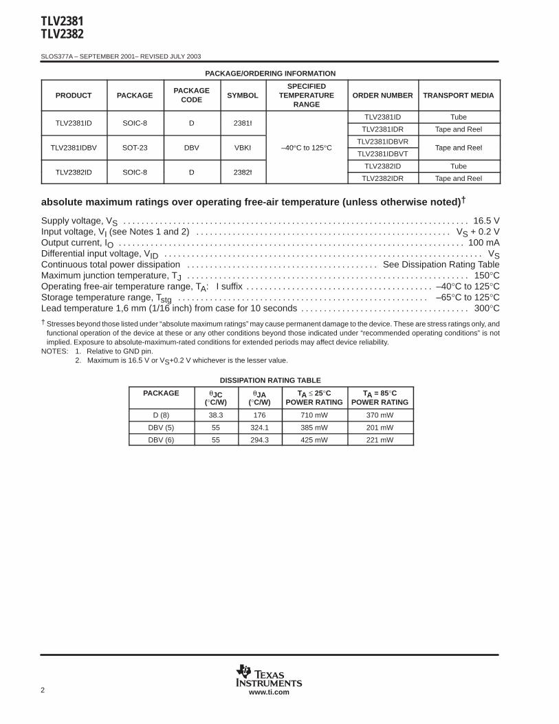
PACKAGE/ORDERING INFORMATION
PRODUCT PACKAGEPACKAGE
CODE SYMBOLSPECIFIED
TEMPERATURERANGE
ORDER NUMBER TRANSPORT MEDIA
TLV2381ID SOIC-8 D 2381I
–40 C to 125 C
TLV2381ID TubeTLV2381ID SOIC-8 D 2381I
–40 C to 125 C
TLV2381IDR Tape and Reel
TLV2381IDBV SOT-23 DBV VBKI –40°C to 125°CTLV2381IDBVR
Tape and ReelTLV2381IDBV SOT-23 DBV VBKI –40°C to 125°CTLV2381IDBVT
Tape and Reel
TLV2382ID SOIC-8 D 2382ITLV2382ID Tube
TLV2382ID SOIC-8 D 2382ITLV2382IDR Tape and Reel
absolute maximum ratings over operating free-air temperature (unless otherwise noted)†
Supply voltage, VS 16.5 V. . . . . . . . . . . . . . . . . . . . . . . . . . . . . . . . . . . . . . . . . . . . . . . . . . . . . . . . . . . . . . . . . . . . . . . . . . . . Input voltage, VI (see Notes 1 and 2) VS + 0.2 V. . . . . . . . . . . . . . . . . . . . . . . . . . . . . . . . . . . . . . . . . . . . . . . . . . . . . . . . Output current, IO 100 mA. . . . . . . . . . . . . . . . . . . . . . . . . . . . . . . . . . . . . . . . . . . . . . . . . . . . . . . . . . . . . . . . . . . . . . . . . . . . Differential input voltage, VID VS. . . . . . . . . . . . . . . . . . . . . . . . . . . . . . . . . . . . . . . . . . . . . . . . . . . . . . . . . . . . . . . . . . . . . . Continuous total power dissipation See Dissipation Rating Table. . . . . . . . . . . . . . . . . . . . . . . . . . . . . . . . . . . . . . . . . . Maximum junction temperature, TJ 150°C. . . . . . . . . . . . . . . . . . . . . . . . . . . . . . . . . . . . . . . . . . . . . . . . . . . . . . . . . . . . . . Operating free-air temperature range, TA: I suffix –40°C to 125°C. . . . . . . . . . . . . . . . . . . . . . . . . . . . . . . . . . . . . . . . . Storage temperature range, Tstg –65°C to 125°C. . . . . . . . . . . . . . . . . . . . . . . . . . . . . . . . . . . . . . . . . . . . . . . . . . . . . . . Lead temperature 1,6 mm (1/16 inch) from case for 10 seconds 300°C. . . . . . . . . . . . . . . . . . . . . . . . . . . . . . . . . . . . .
† Stresses beyond those listed under “absolute maximum ratings” may cause permanent damage to the device. These are stress ratings only, andfunctional operation of the device at these or any other conditions beyond those indicated under “recommended operating conditions” is notimplied. Exposure to absolute-maximum-rated conditions for extended periods may affect device reliability.
NOTES: 1. Relative to GND pin.2. Maximum is 16.5 V or VS+0.2 V whichever is the lesser value.
DISSIPATION RATING TABLE
PACKAGE θJC(°C/W)
θJA(°C/W)
TA ≤ 25°CPOWER RATING
TA = 85°CPOWER RATING
D (8) 38.3 176 710 mW 370 mW
DBV (5) 55 324.1 385 mW 201 mW
DBV (6) 55 294.3 425 mW 221 mW
TLV2381TLV2382
SLOS377A – SEPTEMBER 2001– REVISED JULY 2003
3www.ti.com
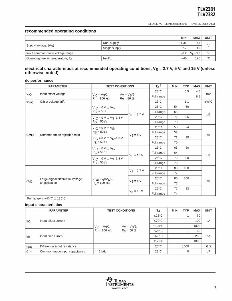
recommended operating conditions
MIN MAX UNIT
Supply voltage, (VS)Dual supply ±1.35 ±8
VSupply voltage, (VS)Single supply 2.7 16
V
Input common-mode voltage range –0.2 VS+0.2 V
Operating free air temperature, TA I-suffix –40 125 °C
electrical characteristics at recommended operating conditions, VS = 2.7 V, 5 V, and 15 V (unlessotherwise noted)
dc performancePARAMETER TEST CONDITIONS TA† MIN TYP MAX UNIT
VIO Input offset voltage VIC = VS/2, VO = VS/225°C 0.5 4.5
mVVIO Input offset voltage VIC = VS/2, VO = VS/2RL = 100 kΩ RS = 50 Ω Full range 6.5
mV
αVIO Offset voltage driftRL = 100 kΩ RS = 50 Ω
25°C 1.1 µV/°C
CMRR Common-mode rejection ratio
VIC = 0 V to VS,
V = 2.7 V
25°C 54 69
dB
CMRR Common-mode rejection ratio
VIC = 0 V to VS, RS = 50 Ω
VS = 2.7 VFull range 53
dB
CMRR Common-mode rejection ratio
VIC = 0 V to VS–1.3 V,VS = 2.7 V
25°C 71 86dB
CMRR Common-mode rejection ratio
VIC = 0 V to VS–1.3 V,RS = 50 Ω Full range 70
CMRR Common-mode rejection ratio
VIC = 0 V to VS,
V = 5 V
25°C 58 74
dBCMRR Common-mode rejection ratio
VIC = 0 V to VS,RS = 50 Ω
VS = 5 VFull range 57
dBCMRR Common-mode rejection ratioVIC = 0 V to VS–1.3 V,
VS = 5 V25°C 72 88
dBVIC = 0 V to VS–1.3 V,RS = 50 Ω Full range 70
VIC = 0 V to VS,
V = 15 V
25°C 65 80
dB
VIC = 0 V to VS,RS = 50 Ω
VS = 15 VFull range 64
dBVIC = 0 V to VS–1.3 V,
VS = 15 V25°C 72 90
dBVIC = 0 V to VS–1.3 V,RS = 50 Ω Full range 70
ALarge-signal differential voltage V =V /2,
VS = 2.7 V25°C 80 100
dBALarge-signal differential voltage V =V /2,
VS = 2.7 VFull range 77
dBAVDLarge-signal differential voltage VO(PP)=VS/2,
VS = 5 V25°C 80 100
dBAVDLarge-signal differential voltageamplification
VO(PP)=VS/2,RL = 100 kΩ VS = 5 V
Full range 77dB
VS = 15 V25°C 77 83
VS = 15 VFull range 74
† Full range is –40°C to 125°C.
input characteristicsPARAMETER TEST CONDITIONS TA MIN TYP MAX UNIT
I Input offset current
V = V /2, V = V /2,
≤25°C 1 60
pAIIO Input offset current
V = V /2, V = V /2,
≤70°C 100 pAIO
VIC = VS/2, VO = VS/2, ≤125°C 1000
I Input bias current
VIC = VS/2, VO = VS/2,RL = 100 kΩ , RS = 50 Ω ≤25°C 1 60
pAIIB Input bias current ≤70°C 200 pAIB≤125°C 1000
ri(d) Differential input resistance 25°C 1000 GΩ
CIC Common-mode input capacitance f = 1 kHz 25°C 8 pF
TLV2381TLV2382
SLOS377A – SEPTEMBER 2001– REVISED JULY 2003
4 www.ti.com
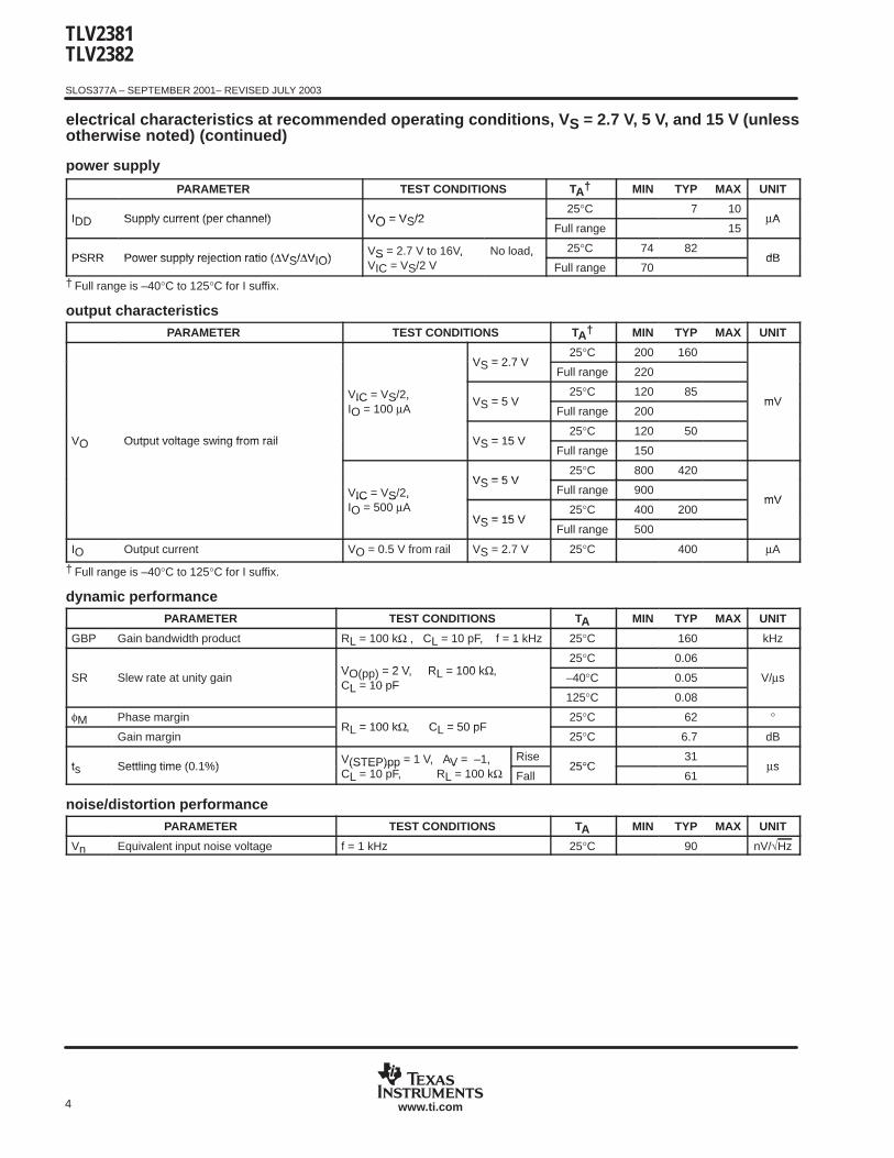
electrical characteristics at recommended operating conditions, VS = 2.7 V, 5 V, and 15 V (unlessotherwise noted) (continued)
power supply
PARAMETER TEST CONDITIONS TA† MIN TYP MAX UNIT
IDD Supply current (per channel) VO = VS/225°C 7 10
µAIDD Supply current (per channel) VO = VS/2Full range 15
µA
PSRR Power supply rejection ratio (∆VS/∆VIO)VS = 2.7 V to 16V, No load, 25°C 74 82
dBPSRR Power supply rejection ratio (∆VS/∆VIO)VS = 2.7 V to 16V,VIC = VS/2 V
No load,Full range 70
dB
† Full range is –40°C to 125°C for I suffix.
output characteristicsPARAMETER TEST CONDITIONS TA† MIN TYP MAX UNIT
V Output voltage swing from rail
V = V /2,
VS = 2.7 V25°C 200 160
mV
V Output voltage swing from rail
V = V /2,
VS = 2.7 VFull range 220
mV
V Output voltage swing from rail
VIC = VS/2,VS = 5 V
25°C 120 85mV
V Output voltage swing from rail
VIC = VS/2,IO = 100 µA
VS = 5 VFull range 200
mV
VO Output voltage swing from rail VS = 15 V25°C 120 50
VO Output voltage swing from rail VS = 15 VFull range 150
V = V /2,VS = 5 V
25°C 800 420
mVVIC = VS/2,
VS = 5 VFull range 900
mVVIC = VS/2,IO = 500 µA
VS = 15 V25°C 400 200
mV
VS = 15 VFull range 500
IO Output current VO = 0.5 V from rail VS = 2.7 V 25°C 400 µA
† Full range is –40°C to 125°C for I suffix.
dynamic performancePARAMETER TEST CONDITIONS TA MIN TYP MAX UNIT
GBP Gain bandwidth product RL = 100 kΩ , CL = 10 pF, f = 1 kHz 25°C 160 kHz
SR Slew rate at unity gainVO(pp) = 2 V, RL = 100 kΩ
25°C 0.06
V/ sSR Slew rate at unity gainVO(pp) = 2 V, RL = 100 kΩ, CL = 10 pF
–40°C 0.05 V/µsCL = 10 pF
125°C 0.08
φM Phase marginRL = 100 kΩ, CL = 50 pF
25°C 62 °
Gain marginRL = 100 kΩ, CL = 50 pF
25°C 6.7 dB
ts Settling time (0.1%)V(STEP)pp = 1 V, AV = –1, Rise
25°C31
µsts Settling time (0.1%)V(STEP)pp = 1 V, AV = –1,CL = 10 pF, RL = 100 kΩ Fall
25°C61
µs
noise/distortion performancePARAMETER TEST CONDITIONS TA MIN TYP MAX UNIT
Vn Equivalent input noise voltage f = 1 kHz 25°C 90 nV/√Hz
TLV2381TLV2382
SLOS377A – SEPTEMBER 2001– REVISED JULY 2003
5www.ti.com
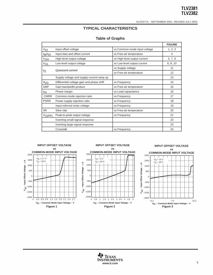
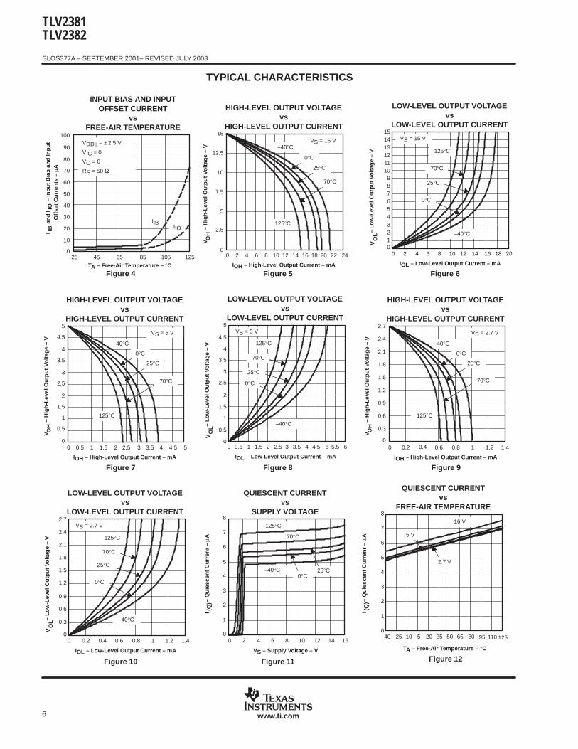
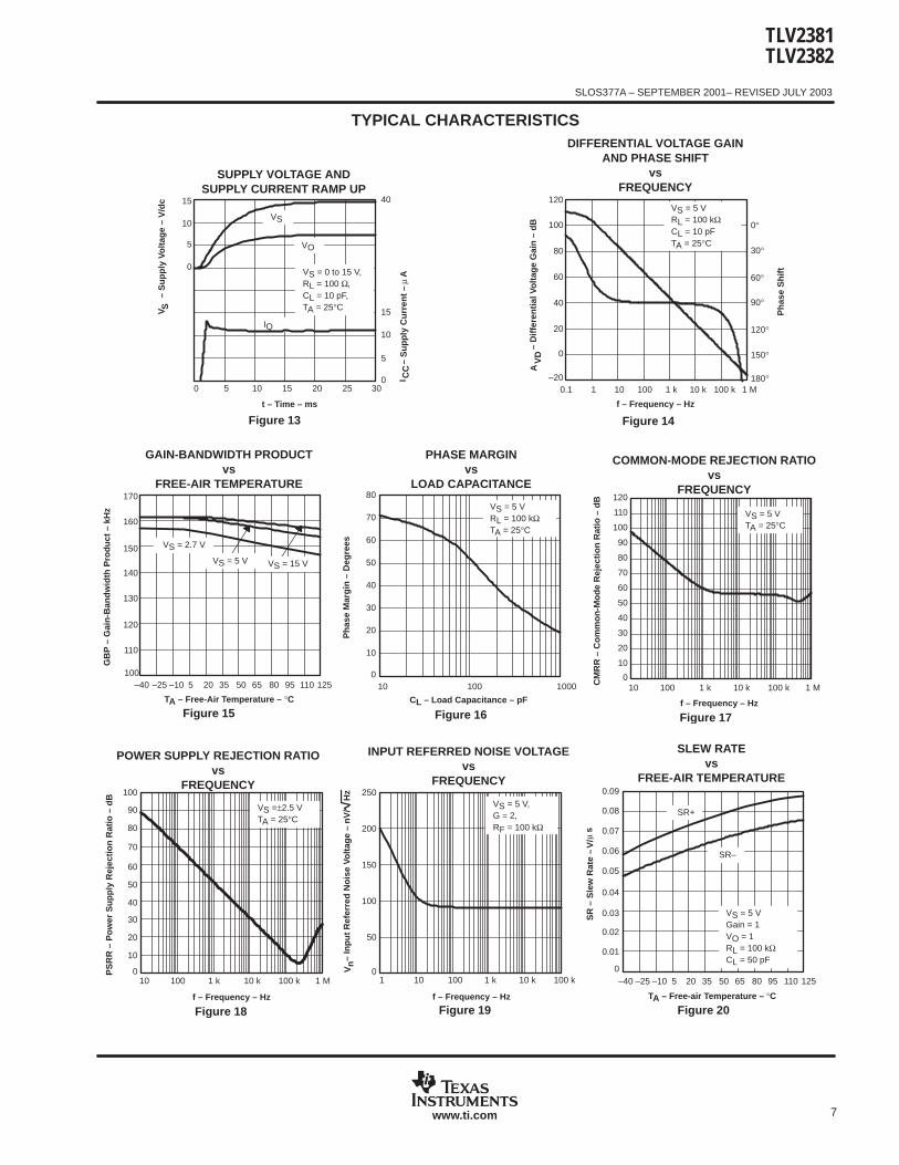
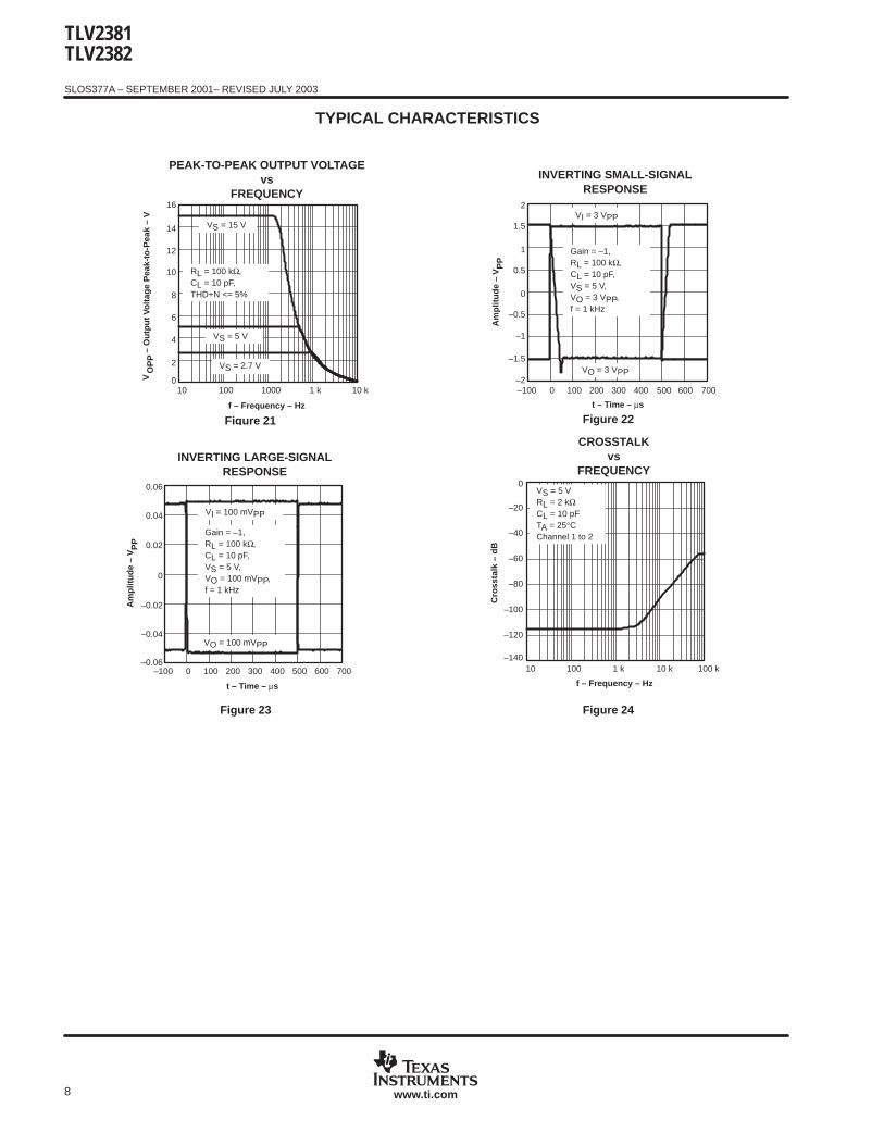
TYPICAL CHARACTERISTICS
Table of Graphs
FIGURE
VIO Input offset voltage vs Common-mode input voltage 1, 2, 3
IIB/IIO Input bias and offset current vs Free-air temperature 4
VOH High-level output voltage vs High-level output current 5, 7, 9
VOL Low-level output voltage vs Low-level output current 6, 8, 10
IQ Quiescent currentvs Supply voltage 11
IQ Quiescent currentvs Free-air temperature 12
Supply voltage and supply current ramp up 13
AVD Differential voltage gain and phase shift vs Frequency 14
GBP Gain-bandwidth product vs Free-air temperature 15
φm Phase margin vs Load capacitance 16
CMRR Common-mode rejection ratio vs Frequency 17
PSRR Power supply rejection ratio vs Frequency 18
Input referred noise voltage vs Frequency 19
SR Slew rate vs Free-air temperature 20
VO(PP) Peak-to-peak output voltage vs Frequency 21
Inverting small-signal response 22
Inverting large-signal response 23
Crosstalk vs Frequency 24
Figure 1
–2000
–1500
–1000
–500
0
500
1000
1500
2000
0 0.3 0.6 0.9 1.2 1.5 1.8 2.1 2.4 2.7
INPUT OFFSET VOLTAGEvs
COMMON-MODE INPUT VOLTAGE
– In
pu
t O
ffse
t Vo
ltag
e –
VIO
Aµ
VIC – Common-Mode Input Voltage – V
VS = 2.7 VTA = 25°C
Figure 2
–2000
–1500
–1000
–500
0
500
1000
1500
2000
0 0.5 1 1.5 2 2.5 3 3.5 4 4.5 5
INPUT OFFSET VOLTAGEvs
COMMON-MODE INPUT VOLTAGE
VIC – Common-Mode Input Voltage – V
– In
pu
t O
ffse
t Vo
ltag
e –
VIO
Aµ
VS = 5 VTA = 25°C
Figure 3
–2000
–1500
–1000
–500
0
500
1000
1500
2000
–0.2 7.5 15.2
INPUT OFFSET VOLTAGEvs
COMMON-MODE INPUT VOLTAGE
VIC – Common-Mode Input Voltage – V
– In
pu
t O
ffse
t Vo
ltag
e –
VIO
Aµ
VS = 15 VTA = 25°C
TLV2381TLV2382
SLOS377A – SEPTEMBER 2001– REVISED JULY 2003
6 www.ti.com
TYPICAL CHARACTERISTICS
Figure 4
– In
pu
t B
ias
and
Inp
ut
INPUT BIAS AND INPUTOFFSET CURRENT
vsFREE-AIR TEMPERATURE
I IB
I IO
TA – Free-Air Temperature – °C
100
90
80
70
60
50
40
30
20
10
025 45 65 85 105 125
VDD± = ± 2.5 V
VIC = 0
VO = 0
RS = 50 Ω
IIBand Off
set
Cu
rren
ts –
pA
IIO
Figure 5
0
2.5
5
7.5
10
12.5
15
200 2 4 6 8 10 12 14 16 18 22 24
–40°C
0°C
25°C
70°C
125°C
VS = 15 V
IOH – High-Level Output Current – mA
– H
igh
-Lev
el O
utp
ut
Volt
age
– V
HIGH-LEVEL OUTPUT VOLTAGEvs
HIGH-LEVEL OUTPUT CURRENT
V OH
Figure 6
0123456789
101112131415
0 2 4 6 8 10 12 14 16 18 20
–40°C
0°C
25°C
125°C
VS = 15 V
70°C
IOL – Low-Level Output Current – mA
– L
ow
-Lev
el O
utp
ut
Volt
age
– V
LOW-LEVEL OUTPUT VOLTAGEvs
LOW-LEVEL OUTPUT CURRENT
VO
L
Figure 7
0
0.5
1
1.5
2
2.5
3
3.5
4
4.5
5
0 0.5 1 1.5 2 2.5 3 3.5 4 4.5 5
–40°C
0°C
25°C
70°C
125°C
VS = 5 V
IOH – High-Level Output Current – mA
– H
igh
-Lev
el O
utp
ut
Volt
age
– V
HIGH-LEVEL OUTPUT VOLTAGEvs
HIGH-LEVEL OUTPUT CURRENT
V OH
Figure 8
0
0.5
1
1.5
2
2.5
3
3.5
4
4.5
5
0 0.5 1 1.5 2 2.5 3 3.5 4 4.5 5 5.5 6
–40°C
0°C
25°C
125°C
VS = 5 V
70°C
IOL – Low-Level Output Current – mA
– L
ow
-Lev
el O
utp
ut
Volt
age
– V
LOW-LEVEL OUTPUT VOLTAGEvs
LOW-LEVEL OUTPUT CURRENT
VO
L
Figure 9
0
0.3
0.6
0.9
1.2
1.5
1.8
2.1
2.4
2.7
0 0.2 0.4 0.6 0.8 1 1.2 1.4
–40°C
0°C
25°C
70°C
125°C
VS = 2.7 V
IOH – High-Level Output Current – mA
– H
igh
-Lev
el O
utp
ut
Volt
age
– V
HIGH-LEVEL OUTPUT VOLTAGEvs
HIGH-LEVEL OUTPUT CURRENT
V OH
Figure 10
0
0.3
0.6
0.9
1.2
1.5
1.8
2.1
2.4
2.7
0 0.2 0.4 0.6 0.8 1 1.2 1.4
–40°C
0°C
25°C
125°C
VS = 2.7 V
70°C
IOL – Low-Level Output Current – mA
– L
ow
-Lev
el O
utp
ut
Volt
age
– V
LOW-LEVEL OUTPUT VOLTAGEvs
LOW-LEVEL OUTPUT CURRENT
VO
L
Figure 11
0
1
2
3
4
5
6
7
8
0 2 4 6 8 10 12 14 16
VS – Supply Voltage – V
QUIESCENT CURRENTvs
SUPPLY VOLTAGE
–40°C 25°C
70°C
125°C
0°C
– Q
uie
scen
t C
urr
enr
– A
µI (
Q)
Figure 12
0
1
2
3
4
5
6
7
8
–40 –25–10 5 20 35 50 65 80 95 110 125
16 V
5 V
2.7 V
TA – Free-Air Temperature – °C
– Q
uie
scen
t C
urr
enr
–
QUIESCENT CURRENTvs
FREE-AIR TEMPERATURE
Aµ
I (Q
)
TLV2381TLV2382
SLOS377A – SEPTEMBER 2001– REVISED JULY 2003
7www.ti.com
TYPICAL CHARACTERISTICS
Figure 13
0
5
10
15
0 5 10 15 20 25 300
5
10
15
40
t – Time – ms
– S
up
ply
Vo
ltag
e –
V/d
c
SUPPLY VOLTAGE ANDSUPPLY CURRENT RAMP UP
– S
up
ply
Cu
rren
t –
V S
Aµ
I CC
VS
VO
IQ
VS = 0 to 15 V,RL = 100 Ω,CL = 10 pF,TA = 25°C
Figure 14
–20
0
20
40
60
80
100
120
0.1 1 10 100 1 k 10 k 100 k 1 M
0°
30°
60°
90°
120°
150°
180°
VS = 5 VRL = 100 kΩCL = 10 pFTA = 25°C
f – Frequency – Hz
– D
iffe
ren
tial
Vo
ltag
e G
ain
– d
B
DIFFERENTIAL VOLTAGE GAINAND PHASE SHIFT
vsFREQUENCY
Ph
ase
Sh
ift
AV
D
Figure 15
100
110
120
130
140
150
160
170
–40 –25 –10 5 20 35 50 65 80 95 110 125
TA – Free-Air Temperature – °C
GB
P –
Gai
n-B
and
wid
th P
rod
uct
– k
Hz
GAIN-BANDWIDTH PRODUCTvs
FREE-AIR TEMPERATURE
VS = 2.7 V
VS = 5 V VS = 15 V
Figure 16
0
10
20
30
40
50
60
70
80
10 100 1000
CL – Load Capacitance – pF
Ph
ase
Mar
gin
– D
egre
es
PHASE MARGINvs
LOAD CAPACITANCE
VS = 5 VRL = 100 kΩTA = 25°C
Figure 17
0
10
20
30
40
50
60
70
80
90
100
110
120
10 100 1 k 10 k 100 k 1 M
VS = 5 VTA = 25°C
f – Frequency – Hz
CM
RR
– C
om
mo
n-M
od
e R
ejec
tio
n R
atio
– d
B
COMMON-MODE REJECTION RATIOvs
FREQUENCY
Figure 18
0
10
20
30
40
50
60
70
80
90
100
10 100 1 k 10 k 100 k 1 M
VS =±2.5 VTA = 25°C
f – Frequency – Hz
PS
RR
– P
ow
er S
up
ply
Rej
ecti
on
Rat
io –
dB
POWER SUPPLY REJECTION RATIOvs
FREQUENCY
Figure 19
0
50
100
150
200
250
1 10 100 1 k 10 k 100 k
VS = 5 V,G = 2,RF = 100 kΩ
f – Frequency – Hz
– In
pu
t R
efer
red
No
ise
Volt
age
–
INPUT REFERRED NOISE VOLTAGEvs
FREQUENCY
nV
/H
zV
n
Figure 20
0
0.01
0.02
0.03
0.04
0.05
0.06
0.07
0.08
0.09
–40 –25 –10 5 20 35 50 65 80 95 110 125
TA – Free-air Temperature – °C
SR
– S
lew
Rat
e –
SLEW RATEvs
FREE-AIR TEMPERATURE
sµ
V/
SR+
SR–
VS = 5 VGain = 1VO = 1RL = 100 kΩCL = 50 pF
TLV2381TLV2382
SLOS377A – SEPTEMBER 2001– REVISED JULY 2003
8 www.ti.com
TYPICAL CHARACTERISTICS
Figure 21
0
2
4
6
8
10
12
14
16
10 100 1000 1 k 10 k
VO
PP
f – Frequency – Hz
– O
utp
ut
Volt
age
Pea
k-to
-Pea
k –
V
PEAK-TO-PEAK OUTPUT VOLTAGEvs
FREQUENCY
VS = 15 V
VS = 5 V
VS = 2.7 V
RL = 100 kΩ,CL = 10 pF,THD+N <= 5%
Figure 22
–2
–1.5
–1
–0.5
0
0.5
1
1.5
2
–100 0 100 200 300 400 500 600 700
VI = 3 VPP
VO = 3 VPP
t – Time – µs
Am
plit
ud
e –
INVERTING SMALL-SIGNALRESPONSE
VP
P
Gain = –1,RL = 100 kΩ,CL = 10 pF,VS = 5 V,VO = 3 VPP,f = 1 kHz
Figure 23
–0.06
–0.04
–0.02
0
0.02
0.04
0.06
–100 0 100 200 300 400 500 600 700
VI = 100 mVPP
VO = 100 mVPP
t – Time – µs
Am
plit
ud
e –
INVERTING LARGE-SIGNALRESPONSE
VP
P
Gain = –1,RL = 100 kΩ,CL = 10 pF,VS = 5 V,VO = 100 mVPP,f = 1 kHz
Figure 24
–140
–120
–100
–80
–60
–40
–20
0
10 100 1 k 10 k 100 k
VS = 5 VRL = 2 kΩCL = 10 pFTA = 25°CChannel 1 to 2
f – Frequency – Hz
Cro
ssta
lk –
dB
CROSSTALKvs
FREQUENCY
TLV2381TLV2382
SLOS377A – SEPTEMBER 2001– REVISED JULY 2003
9www.ti.com
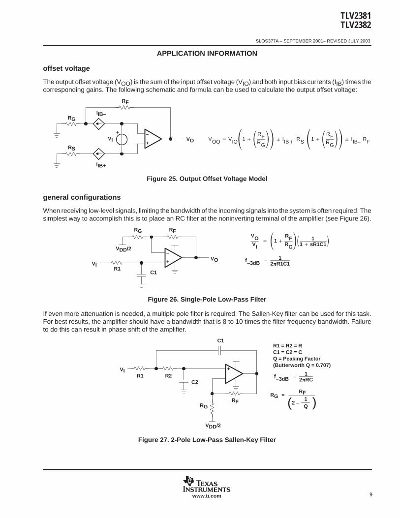
APPLICATION INFORMATION
offset voltage
The output offset voltage (VOO) is the sum of the input offset voltage (VIO) and both input bias currents (IIB) times thecorresponding gains. The following schematic and formula can be used to calculate the output offset voltage:
VOO VIO1RFRG IIB RS 1RF
RG IIB– RF+
–VI
+
RG
RS
RF
IIB–
VO
IIB+
Figure 25. Output Offset Voltage Model
general configurations
When receiving low-level signals, limiting the bandwidth of the incoming signals into the system is often required. Thesimplest way to accomplish this is to place an RC filter at the noninverting terminal of the amplifier (see Figure 26).
VIVO
C1
+
–
RG RF
R1
f–3dB 12R1C1
VOVI
1 RFRG 1
1 sR1C1
VDD/2
Figure 26. Single-Pole Low-Pass Filter
If even more attenuation is needed, a multiple pole filter is required. The Sallen-Key filter can be used for this task.For best results, the amplifier should have a bandwidth that is 8 to 10 times the filter frequency bandwidth. Failureto do this can result in phase shift of the amplifier.
VI
C2R2R1
C1
RFRG
R1 = R2 = RC1 = C2 = CQ = Peaking Factor(Butterworth Q = 0.707)
(=
1Q
2 – )RG
RF
_+
f–3dB 12RC
VDD/2
Figure 27. 2-Pole Low-Pass Sallen-Key Filter
TLV2381TLV2382
SLOS377A – SEPTEMBER 2001– REVISED JULY 2003
10 www.ti.com
APPLICATION INFORMATION
circuit layout considerations
To achieve the levels of high performance of the TLV238x, follow proper printed-circuit board design techniques. Ageneral set of guidelines is given in the following.
Ground planes—It is highly recommended that a ground plane be used on the board to provide allcomponents with a low inductive ground connection. However, in the areas of the amplifier inputs andoutput, the ground plane can be removed to minimize the stray capacitance.
Proper power supply decoupling—Use a 6.8-µF tantalum capacitor in parallel with a 0.1-µF ceramiccapacitor on each supply terminal. It may be possible to share the tantalum among several amplifiersdepending on the application, but a 0.1-µF ceramic capacitor should always be used on the supply terminalof every amplifier. In addition, the 0.1-µF capacitor should be placed as close as possible to the supplyterminal. As this distance increases, the inductance in the connecting trace makes the capacitor lesseffective. The designer should strive for distances of less than 0.1 inches between the device powerterminals and the ceramic capacitors.
Sockets—Sockets can be used but are not recommended. The additional lead inductance in the socket pinswill often lead to stability problems. Surface-mount packages soldered directly to the printed-circuit boardis the best implementation.
Short trace runs/compact part placements—Optimum high performance is achieved when stray seriesinductance has been minimized. To realize this, the circuit layout should be made as compact as possible,thereby minimizing the length of all trace runs. Particular attention should be paid to the inverting input ofthe amplifier. Its length should be kept as short as possible. This will help to minimize stray capacitance atthe input of the amplifier.
Surface-mount passive components—Using surface-mount passive components is recommended for highperformance amplifier circuits for several reasons. First, because of the extremely low lead inductance ofsurface-mount components, the problem with stray series inductance is greatly reduced. Second, the smallsize of surface-mount components naturally leads to a more compact layout thereby minimizing both strayinductance and capacitance. If leaded components are used, it is recommended that the lead lengths bekept as short as possible.
TLV2381TLV2382
SLOS377A – SEPTEMBER 2001– REVISED JULY 2003
11www.ti.com
APPLICATION INFORMATION
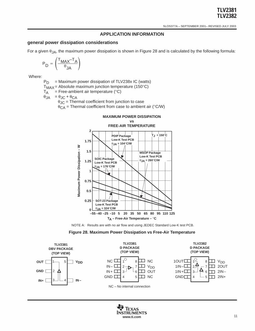
general power dissipation considerations
For a given θJA, the maximum power dissipation is shown in Figure 28 and is calculated by the following formula:
PD TMAX–TAJA
Where:
PD = Maximum power dissipation of TLV238x IC (watts)TMAX= Absolute maximum junction temperature (150°C)TA = Free-ambient air temperature (°C)θJA = θJC + θCA
θJC = Thermal coefficient from junction to case θCA = Thermal coefficient from case to ambient air (°C/W)
1
0.75
0.5
0–55 –40 –25 –10 5
Max
imu
m P
ow
er D
issi
pat
ion
– W
1.25
1.5
MAXIMUM POWER DISSIPATIONvs
FREE-AIR TEMPERATURE
1.75
20 35 50
0.25
TA – Free-Air Temperature – °C
2
65 80 95 110 125
MSOP PackageLow-K Test PCBθJA = 260°C/W
TJ = 150°CPDIP PackageLow-K Test PCBθJA = 104°C/W
SOIC PackageLow-K Test PCBθJA = 176°C/W
SOT-23 PackageLow-K Test PCBθJA = 324°C/W
NOTE A: Results are with no air flow and using JEDEC Standard Low-K test PCB.
Figure 28. Maximum Power Dissipation vs Free-Air Temperature
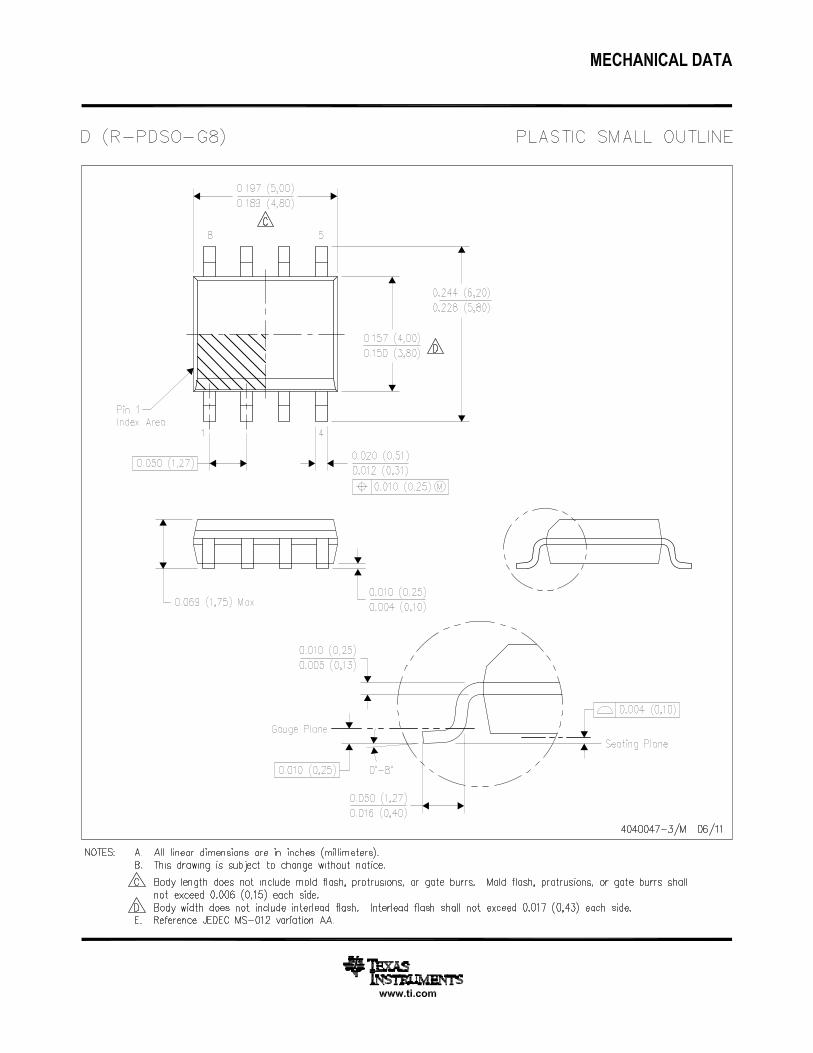
3
2
4
5
(TOP VIEW)
1OUT
GND
IN+
VDD
IN–
TLV2381DBV PACKAGE
1
2
3
4
8
7
6
5
NCIN–IN+
GND
NCVDDOUTNC
TLV2381D PACKAGE(TOP VIEW)
1
2
3
4
8
7
6
5
1OUT1IN–1IN+GND
VDD2OUT2IN–2IN+
TLV2382D PACKAGE(TOP VIEW)
NC – No internal connection
PACKAGE OPTION ADDENDUM
www.ti.com 15-Apr-2017
Addendum-Page 1
PACKAGING INFORMATION
Orderable Device Status(1)
Package Type PackageDrawing
Pins PackageQty
Eco Plan(2)
Lead/Ball Finish(6)
MSL Peak Temp(3)
Op Temp (°C) Device Marking(4/5)
Samples
TLV2381ID ACTIVE SOIC D 8 75 Green (RoHS& no Sb/Br)
CU NIPDAU Level-1-260C-UNLIM -40 to 125 2381I
TLV2381IDBVR ACTIVE SOT-23 DBV 5 3000 Green (RoHS& no Sb/Br)
CU NIPDAU Level-1-260C-UNLIM -40 to 125 VBKI
TLV2381IDBVRG4 ACTIVE SOT-23 DBV 5 3000 Green (RoHS& no Sb/Br)
CU NIPDAU Level-1-260C-UNLIM -40 to 125 VBKI
TLV2381IDBVT ACTIVE SOT-23 DBV 5 250 Green (RoHS& no Sb/Br)
CU NIPDAU Level-1-260C-UNLIM -40 to 125 VBKI
TLV2381IDBVTG4 ACTIVE SOT-23 DBV 5 250 Green (RoHS& no Sb/Br)
CU NIPDAU Level-1-260C-UNLIM -40 to 125 VBKI
TLV2381IDG4 ACTIVE SOIC D 8 75 Green (RoHS& no Sb/Br)
CU NIPDAU Level-1-260C-UNLIM -40 to 125 2381I
TLV2381IDR ACTIVE SOIC D 8 2500 Green (RoHS& no Sb/Br)
CU NIPDAU Level-1-260C-UNLIM -40 to 125 2381I
TLV2382ID ACTIVE SOIC D 8 75 Green (RoHS& no Sb/Br)
CU NIPDAU Level-1-260C-UNLIM -40 to 125 2382I
TLV2382IDG4 ACTIVE SOIC D 8 75 Green (RoHS& no Sb/Br)
CU NIPDAU Level-1-260C-UNLIM -40 to 125 2382I
TLV2382IDR ACTIVE SOIC D 8 2500 Green (RoHS& no Sb/Br)
CU NIPDAU Level-1-260C-UNLIM -40 to 125 2382I
TLV2382IDRG4 ACTIVE SOIC D 8 2500 Green (RoHS& no Sb/Br)
CU NIPDAU Level-1-260C-UNLIM -40 to 125 2382I
(1) The marketing status values are defined as follows:ACTIVE: Product device recommended for new designs.LIFEBUY: TI has announced that the device will be discontinued, and a lifetime-buy period is in effect.NRND: Not recommended for new designs. Device is in production to support existing customers, but TI does not recommend using this part in a new design.PREVIEW: Device has been announced but is not in production. Samples may or may not be available.OBSOLETE: TI has discontinued the production of the device.
(2) Eco Plan - The planned eco-friendly classification: Pb-Free (RoHS), Pb-Free (RoHS Exempt), or Green (RoHS & no Sb/Br) - please check http://www.ti.com/productcontent for the latest availabilityinformation and additional product content details.TBD: The Pb-Free/Green conversion plan has not been defined.Pb-Free (RoHS): TI's terms "Lead-Free" or "Pb-Free" mean semiconductor products that are compatible with the current RoHS requirements for all 6 substances, including the requirement thatlead not exceed 0.1% by weight in homogeneous materials. Where designed to be soldered at high temperatures, TI Pb-Free products are suitable for use in specified lead-free processes.
PACKAGE OPTION ADDENDUM
www.ti.com 15-Apr-2017
Addendum-Page 2
Pb-Free (RoHS Exempt): This component has a RoHS exemption for either 1) lead-based flip-chip solder bumps used between the die and package, or 2) lead-based die adhesive used betweenthe die and leadframe. The component is otherwise considered Pb-Free (RoHS compatible) as defined above.Green (RoHS & no Sb/Br): TI defines "Green" to mean Pb-Free (RoHS compatible), and free of Bromine (Br) and Antimony (Sb) based flame retardants (Br or Sb do not exceed 0.1% by weightin homogeneous material)
(3) MSL, Peak Temp. - The Moisture Sensitivity Level rating according to the JEDEC industry standard classifications, and peak solder temperature.
(4) There may be additional marking, which relates to the logo, the lot trace code information, or the environmental category on the device.
(5) Multiple Device Markings will be inside parentheses. Only one Device Marking contained in parentheses and separated by a "~" will appear on a device. If a line is indented then it is a continuationof the previous line and the two combined represent the entire Device Marking for that device.
(6) Lead/Ball Finish - Orderable Devices may have multiple material finish options. Finish options are separated by a vertical ruled line. Lead/Ball Finish values may wrap to two lines if the finishvalue exceeds the maximum column width.
Important Information and Disclaimer:The information provided on this page represents TI's knowledge and belief as of the date that it is provided. TI bases its knowledge and belief on informationprovided by third parties, and makes no representation or warranty as to the accuracy of such information. Efforts are underway to better integrate information from third parties. TI has taken andcontinues to take reasonable steps to provide representative and accurate information but may not have conducted destructive testing or chemical analysis on incoming materials and chemicals.TI and TI suppliers consider certain information to be proprietary, and thus CAS numbers and other limited information may not be available for release.
In no event shall TI's liability arising out of such information exceed the total purchase price of the TI part(s) at issue in this document sold by TI to Customer on an annual basis.
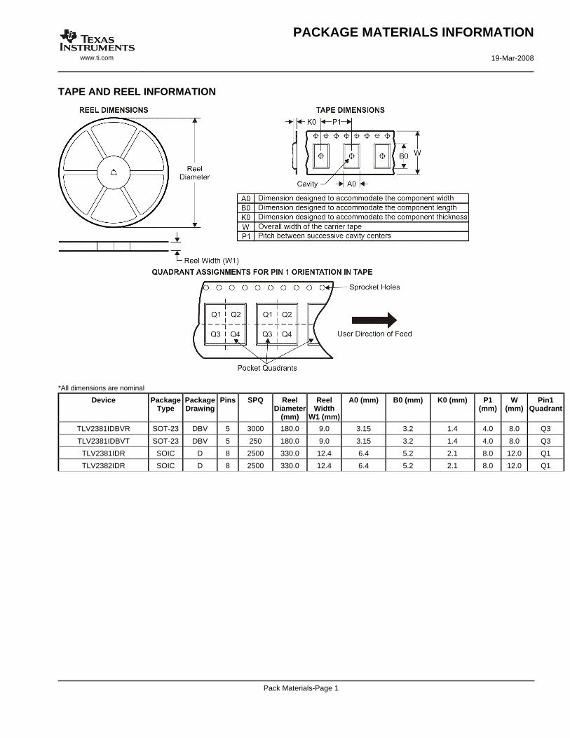
TAPE AND REEL INFORMATION
*All dimensions are nominal
Device PackageType
PackageDrawing
Pins SPQ ReelDiameter
(mm)
ReelWidth
W1 (mm)
A0 (mm) B0 (mm) K0 (mm) P1(mm)
W(mm)
Pin1Quadrant
TLV2381IDBVR SOT-23 DBV 5 3000 180.0 9.0 3.15 3.2 1.4 4.0 8.0 Q3
TLV2381IDBVT SOT-23 DBV 5 250 180.0 9.0 3.15 3.2 1.4 4.0 8.0 Q3
TLV2381IDR SOIC D 8 2500 330.0 12.4 6.4 5.2 2.1 8.0 12.0 Q1
TLV2382IDR SOIC D 8 2500 330.0 12.4 6.4 5.2 2.1 8.0 12.0 Q1
PACKAGE MATERIALS INFORMATION
www.ti.com 19-Mar-2008
Pack Materials-Page 1
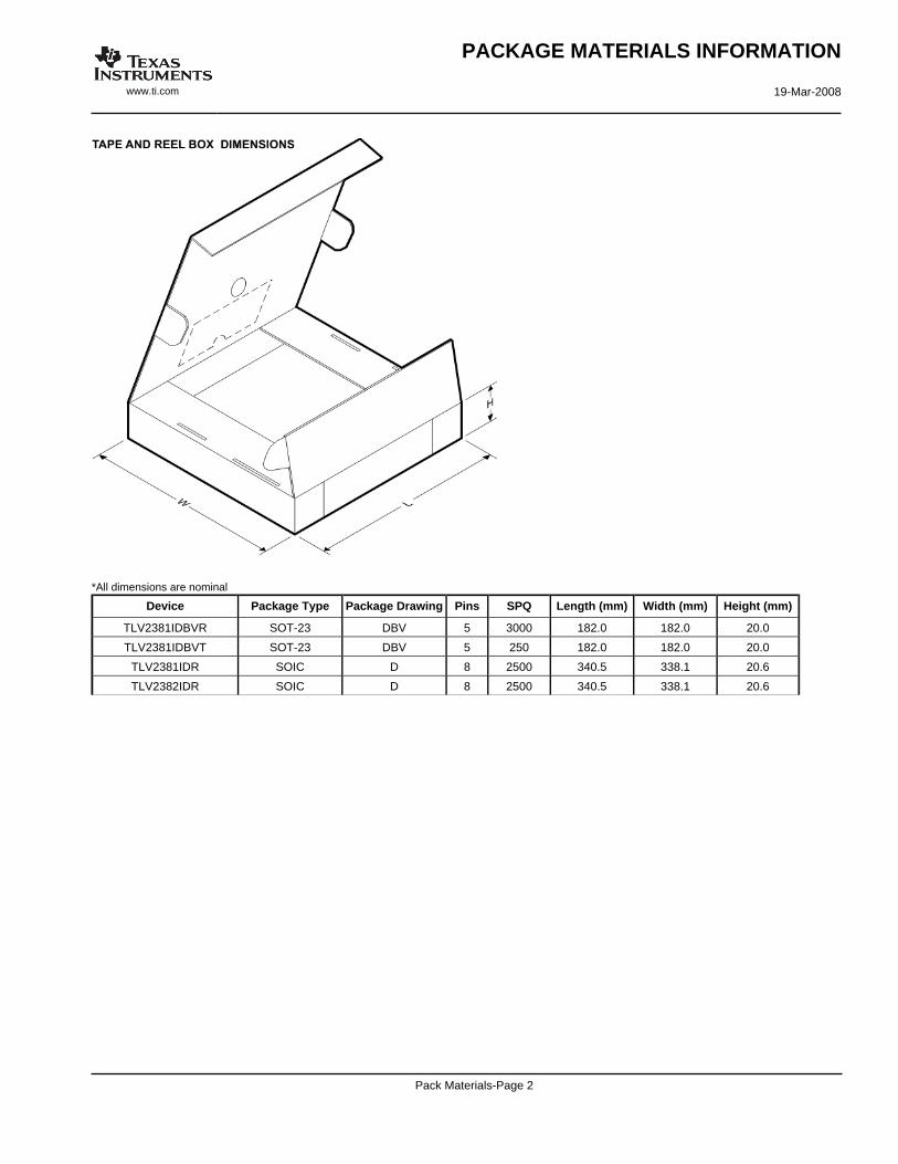
*All dimensions are nominal
Device Package Type Package Drawing Pins SPQ Length (mm) Width (mm) Height (mm)
TLV2381IDBVR SOT-23 DBV 5 3000 182.0 182.0 20.0
TLV2381IDBVT SOT-23 DBV 5 250 182.0 182.0 20.0
TLV2381IDR SOIC D 8 2500 340.5 338.1 20.6
TLV2382IDR SOIC D 8 2500 340.5 338.1 20.6
PACKAGE MATERIALS INFORMATION
www.ti.com 19-Mar-2008
Pack Materials-Page 2
IMPORTANT NOTICE
Texas Instruments Incorporated (TI) reserves the right to make corrections, enhancements, improvements and other changes to itssemiconductor products and services per JESD46, latest issue, and to discontinue any product or service per JESD48, latest issue. Buyersshould obtain the latest relevant information before placing orders and should verify that such information is current and complete.TI’s published terms of sale for semiconductor products (http://www.ti.com/sc/docs/stdterms.htm) apply to the sale of packaged integratedcircuit products that TI has qualified and released to market. Additional terms may apply to the use or sale of other types of TI products andservices.Reproduction of significant portions of TI information in TI data sheets is permissible only if reproduction is without alteration and isaccompanied by all associated warranties, conditions, limitations, and notices. TI is not responsible or liable for such reproduceddocumentation. Information of third parties may be subject to additional restrictions. Resale of TI products or services with statementsdifferent from or beyond the parameters stated by TI for that product or service voids all express and any implied warranties for theassociated TI product or service and is an unfair and deceptive business practice. TI is not responsible or liable for any such statements.Buyers and others who are developing systems that incorporate TI products (collectively, “Designers”) understand and agree that Designersremain responsible for using their independent analysis, evaluation and judgment in designing their applications and that Designers havefull and exclusive responsibility to assure the safety of Designers' applications and compliance of their applications (and of all TI productsused in or for Designers’ applications) with all applicable regulations, laws and other applicable requirements. Designer represents that, withrespect to their applications, Designer has all the necessary expertise to create and implement safeguards that (1) anticipate dangerousconsequences of failures, (2) monitor failures and their consequences, and (3) lessen the likelihood of failures that might cause harm andtake appropriate actions. Designer agrees that prior to using or distributing any applications that include TI products, Designer willthoroughly test such applications and the functionality of such TI products as used in such applications.TI’s provision of technical, application or other design advice, quality characterization, reliability data or other services or information,including, but not limited to, reference designs and materials relating to evaluation modules, (collectively, “TI Resources”) are intended toassist designers who are developing applications that incorporate TI products; by downloading, accessing or using TI Resources in anyway, Designer (individually or, if Designer is acting on behalf of a company, Designer’s company) agrees to use any particular TI Resourcesolely for this purpose and subject to the terms of this Notice.TI’s provision of TI Resources does not expand or otherwise alter TI’s applicable published warranties or warranty disclaimers for TIproducts, and no additional obligations or liabilities arise from TI providing such TI Resources. TI reserves the right to make corrections,enhancements, improvements and other changes to its TI Resources. TI has not conducted any testing other than that specificallydescribed in the published documentation for a particular TI Resource.Designer is authorized to use, copy and modify any individual TI Resource only in connection with the development of applications thatinclude the TI product(s) identified in such TI Resource. NO OTHER LICENSE, EXPRESS OR IMPLIED, BY ESTOPPEL OR OTHERWISETO ANY OTHER TI INTELLECTUAL PROPERTY RIGHT, AND NO LICENSE TO ANY TECHNOLOGY OR INTELLECTUAL PROPERTYRIGHT OF TI OR ANY THIRD PARTY IS GRANTED HEREIN, including but not limited to any patent right, copyright, mask work right, orother intellectual property right relating to any combination, machine, or process in which TI products or services are used. Informationregarding or referencing third-party products or services does not constitute a license to use such products or services, or a warranty orendorsement thereof. Use of TI Resources may require a license from a third party under the patents or other intellectual property of thethird party, or a license from TI under the patents or other intellectual property of TI.TI RESOURCES ARE PROVIDED “AS IS” AND WITH ALL FAULTS. TI DISCLAIMS ALL OTHER WARRANTIES ORREPRESENTATIONS, EXPRESS OR IMPLIED, REGARDING RESOURCES OR USE THEREOF, INCLUDING BUT NOT LIMITED TOACCURACY OR COMPLETENESS, TITLE, ANY EPIDEMIC FAILURE WARRANTY AND ANY IMPLIED WARRANTIES OFMERCHANTABILITY, FITNESS FOR A PARTICULAR PURPOSE, AND NON-INFRINGEMENT OF ANY THIRD PARTY INTELLECTUALPROPERTY RIGHTS. TI SHALL NOT BE LIABLE FOR AND SHALL NOT DEFEND OR INDEMNIFY DESIGNER AGAINST ANY CLAIM,INCLUDING BUT NOT LIMITED TO ANY INFRINGEMENT CLAIM THAT RELATES TO OR IS BASED ON ANY COMBINATION OFPRODUCTS EVEN IF DESCRIBED IN TI RESOURCES OR OTHERWISE. IN NO EVENT SHALL TI BE LIABLE FOR ANY ACTUAL,DIRECT, SPECIAL, COLLATERAL, INDIRECT, PUNITIVE, INCIDENTAL, CONSEQUENTIAL OR EXEMPLARY DAMAGES INCONNECTION WITH OR ARISING OUT OF TI RESOURCES OR USE THEREOF, AND REGARDLESS OF WHETHER TI HAS BEENADVISED OF THE POSSIBILITY OF SUCH DAMAGES.Unless TI has explicitly designated an individual product as meeting the requirements of a particular industry standard (e.g., ISO/TS 16949and ISO 26262), TI is not responsible for any failure to meet such industry standard requirements.Where TI specifically promotes products as facilitating functional safety or as compliant with industry functional safety standards, suchproducts are intended to help enable customers to design and create their own applications that meet applicable functional safety standardsand requirements. Using products in an application does not by itself establish any safety features in the application. Designers mustensure compliance with safety-related requirements and standards applicable to their applications. Designer may not use any TI products inlife-critical medical equipment unless authorized officers of the parties have executed a special contract specifically governing such use.Life-critical medical equipment is medical equipment where failure of such equipment would cause serious bodily injury or death (e.g., lifesupport, pacemakers, defibrillators, heart pumps, neurostimulators, and implantables). Such equipment includes, without limitation, allmedical devices identified by the U.S. Food and Drug Administration as Class III devices and equivalent classifications outside the U.S.TI may expressly designate certain products as completing a particular qualification (e.g., Q100, Military Grade, or Enhanced Product).Designers agree that it has the necessary expertise to select the product with the appropriate qualification designation for their applicationsand that proper product selection is at Designers’ own risk. Designers are solely responsible for compliance with all legal and regulatoryrequirements in connection with such selection.Designer will fully indemnify TI and its representatives against any damages, costs, losses, and/or liabilities arising out of Designer’s non-compliance with the terms and provisions of this Notice.
Mailing Address: Texas Instruments, Post Office Box 655303, Dallas, Texas 75265Copyright © 2018, Texas Instruments Incorporated