Fabrication of gold microelectrodes on glass substrate by … · 2012-11-10 · Fabrication of Gold...
5
JLMN-Journal of Laser Micro/Nanoengineering Vol. 7, No. 3, 2012 334 Fabrication of Gold Microelectrodes on a Glass Substrate by Femtosecond-Laser-Assisted Electroless Plating Jiangxin Song *1 , Yang Liao *1 , Changning Liu *1 , Di Lin *1 , Lingling Qiao *1 , Ya Cheng *1 † ,Koji Sugioka *2 , Katsumi Midorikawa *2 , Shan Zhang *3 *1 State Key Laboratory of High Field Laser Physics, Shanghai Institute of Optics and Fine Mechanics, Chinese Academy of Sciences, P.O. Box 800-211, Shanghai 201800, China *2 Laser Technology Laboratory, RIKEN- Advanced Science Institute, 2-1 Hirosawa, Wako, Saitama 351-0198, Japan *3 Key Laboratory of Infrared Imaging Material and Detectors Shanghai Institute of Technical Physics, Chinese Academy of Sciences, Shanghai 200083, China † Email: [email protected] We present a simple method for fabrication of gold microelectrode by use of femtosecond laser modification combined with successive electroless gold plating. The fabrication procedures mainly include (1) femtosecond laser direct writing for generation of silver seeds, (2) electroless plating for selective growth of gold in areas modified by femtosecond laser irradiation, and (3) postannealing at 300 °C for 1 hr for improving adhesion. We find that for successfully achieving selective deposition of gold, the composition of plating solution needs to be carefully chosen and optimized. We demonstrate good electrical conductivity and excellently adhesion of the microelectrode. Keywords: gold microelectrode, femtosecond laser, glass, electroless plating Introduction In the past decade, lab-on-a-chip (LOC) technology have attracted increasing attention [1-2] because of its capability of downsizing chemistry and biology using highly integrated micro-devices. Common functions required by LOC devices include microfluidics, micro-optics, micromechanics, and micro-electrodes. Recently, it has been shown that femtosecond laser source, which is a tool for ultrafast science research [3], can be employed for fabrication and integration of multi-functional components in glass, making it an ideal tool for manufacturing of LOC systems [4-6]. In particular, fabrication of microelectrodes has been demonstrated with femtosecond laser direct writing and successive electroless copper plating [7-8], which has been used for electro-optic integration or construction of micro-heaters on microfluidic chips [9]. However, for some important analysis applications, copper cannot be used because of its insufficient chemical inertness. On the other hand, due to its stable chemical and excellent physical properties, gold microelectrode has become an important component of lab-on-a-chip devices for many applications, such as single molecular detection [10], electrophoresis analysis [11] and surface-enhanced Raman scattering (SERS) [12-13]. The conventional deposition methods for gold microelectrode are vacuum evaporation [14], electrodeposition [15] and electroless plating [16-18]. Among them, the electroless plating technique is a simple and cost-efficient approach in which metal deposition can be achieved in ambient conditions without the use of any electrical potential. Nevertheless, so far, electroless plating of gold in a space-selective manner with femtosecond laser direct writing has not been demonstrated, which will enable one-step integration of a series of functionalities into LOC devices. In this work, we attempt to fabricate gold
Transcript of Fabrication of gold microelectrodes on glass substrate by … · 2012-11-10 · Fabrication of Gold...
JLMN-Journal of Laser Micro/Nanoengineering Vol. 7, No. 3, 2012
334
Fabrication of Gold Microelectrodes on a Glass Substrate by
Femtosecond-Laser-Assisted Electroless Plating
Jiangxin Song*1, Yang Liao*1, Changning Liu*1, Di Lin*1, Lingling Qiao*1, Ya Cheng*1†,Koji Sugioka*2, Katsumi Midorikawa*2, Shan Zhang*3 *1State Key Laboratory of High Field Laser Physics, Shanghai Institute of Optics and Fine Mechanics, Chinese Academy of
Sciences, P.O. Box 800-211, Shanghai 201800, China *2Laser Technology Laboratory, RIKEN- Advanced Science Institute, 2-1 Hirosawa, Wako, Saitama 351-0198, Japan *3Key Laboratory of Infrared Imaging Material and Detectors Shanghai Institute of Technical Physics, Chinese Academy of Sciences, Shanghai 200083, China
†Email: [email protected]
We present a simple method for fabrication of gold microelectrode by use of femtosecond laser modification combined with successive electroless gold plating. The fabrication procedures mainly include (1) femtosecond laser direct writing for generation of silver seeds, (2) electroless plating for selective growth of gold in areas modified by femtosecond laser irradiation, and (3) postannealing at 300 °C for 1 hr for improving adhesion. We find that for successfully achieving selective deposition of gold, the composition of plating solution needs to be carefully chosen and optimized. We demonstrate good electrical conductivity and excellently adhesion of the microelectrode.
Keywords: gold microelectrode, femtosecond laser, glass, electroless plating
Introduction
In the past decade, lab-on-a-chip (LOC) technology have attracted increasing attention [1-2] because of its capability of downsizing chemistry and biology using highly integrated micro-devices. Common functions required by LOC devices include microfluidics, micro-optics, micromechanics, and micro-electrodes. Recently, it has been shown that femtosecond laser source, which is a tool for ultrafast science research [3], can be employed for fabrication and integration of multi-functional components in glass, making it an ideal tool for manufacturing of LOC systems [4-6]. In particular, fabrication of microelectrodes has been demonstrated with femtosecond laser direct writing and successive electroless copper plating [7-8], which has been used for electro-optic integration or construction of micro-heaters on
microfluidic chips [9]. However, for some important analysis applications, copper cannot be used because of its insufficient chemical inertness. On the other hand, due to its stable chemical and excellent physical properties, gold microelectrode has become an important component of lab-on-a-chip devices for many applications, such as single molecular detection [10], electrophoresis analysis [11] and surface-enhanced Raman scattering (SERS) [12-13]. The conventional deposition methods for gold microelectrode are vacuum evaporation [14], electrodeposition [15] and electroless plating [16-18]. Among them, the electroless plating technique is a simple and cost-efficient approach in which metal deposition can be achieved in ambient conditions without the use of any electrical potential. Nevertheless, so far, electroless plating of gold in a space-selective manner with femtosecond laser direct writing has not been demonstrated, which will enable one-step integration of a series of functionalities into LOC devices. In this work, we attempt to fabricate gold
Hiromi
タイプライターテキスト
DOI:10.2961/jlmn.2012.03.0018
JLMN-Journal of Laser Micro/Nanoengineering Vol. 7, No. 3, 2012
335
microelectrodes in fused silica glass using femtosecond laser direct writing followed by electroless gold plating process. We found that for successfully achieving selective deposition of gold in the femtosecond laser modified areas on the fused silica substrate, the composition of plating solution needs to be carefully chosen and optimized, otherwise no plating could occur. The adhesion of the gold electrodes, which is not sufficiently strong after the electroless plating, can be significantly improved by a postannealing process.
Experimental
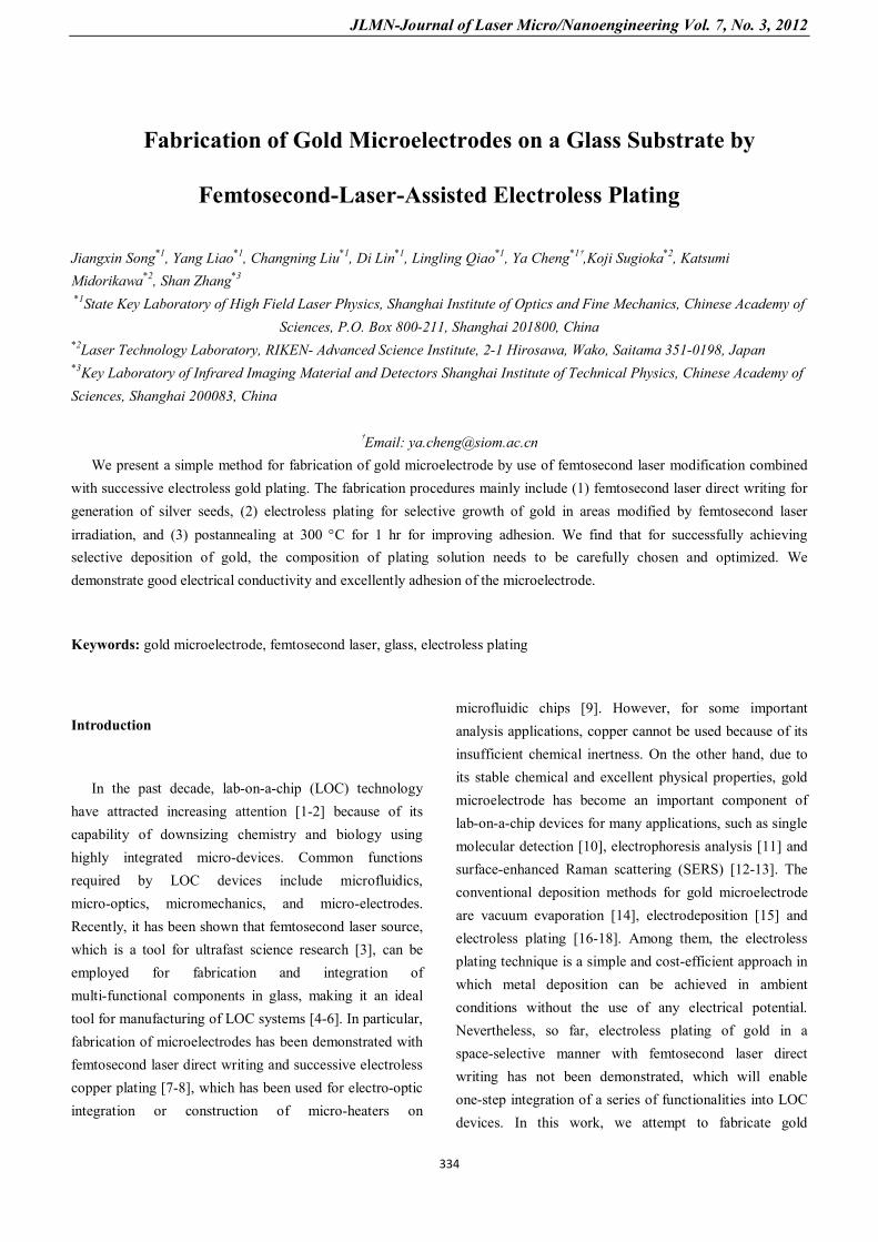
The detailed fabrication procedures are illustrated in Figure 1 which include five steps: (a) femtosecond laser ablation; (b) coating AgNO3 solution; (c) depositon of silver seeds; (d) electroless gold plating; and (e) enhancing adhesion microelectrode by postannealing. The experimental setup for the femtosecond laser direct writing consists of a Ti: sapphire oscillator (Coherent, Inc.) and a regenerative amplifier, with an operating wavelength of 800nm, a pulse width of 50 fs, and a repetition frequency of 250 kHz. The laser beam was focused by an objective lens (20×, NA=0.45) onto the glass surface, and the sample can be arbitrarily translated by a PC-controlled XYZ stage with a resolution of 1 µm. The laser pulse energy can be adjusted using neutral density (ND) filters and the laser power was monitored using an energy meter. Commercially available glass samples (quartz glass) polished on four sides was used as substrates in this study and the experimental details are as follows: Micro-grooves were formed on the glass surface by femtosecond laser ablation at a 200 mw average power using a 20× objective (NA=0.45). The depth of grooves is about 15 µm. The scan speed of the step in Fig.1(a) is 1mm/s. The grooves are fabricated by overlapping multiple ablation lines in the direction perpendicular to the grooves. In our experiment, the spacing between two adjacent lines is fixed as 1 µm. Thus, the number of scans of the step in Fig. 1(a) is determined by the width of the groove. Meanwhile, it is noteworthy that without this femtosecond laser ablation (i. e., the step (a) in Fig. 1), it is still possible to achieve electroless plating of gold by performing only the remaining procedures. However, the adhesion of the
microelectrodes coated on the smooth surface of the substrate will be much worse. On the other hand, this ablation step will allow formation of gold wires embedded in the glass substrate, which may be useful for 3D integration as we have demonstrated in Ref. 19. Thus, the role of the ablation step is to create the grooves and the roughness required for ensuring a strong adhesion.
After the dip-coating of the ablated glass sampled with AgNO3 solution (0.5M/L) (step in Fig. 1(b)), the grooves were scanned using the same objective but at a lower power (about 8mw). It is found that the grooves turn to black (step in Fig. 1(c)), suggesting that silver nanoparticles were formed in the grooves which will serve as seeds for the successive electroless gold plating. It should be noted that the scan speed must be reduced for the step in Fig. 1(c) because to ensure deposition of a sufficient amount of silver seeds in the groove, the scan of step in Fig. 1(c) was operated manually. During the scan, we monitor the sample under the microscope in real time. When high-quality deposition of silver nanoparticles in the grooves occurs, we can observe that the color of the groove becomes dark due to the absorption of light by the silver nanoparticles. If the darkening of groove is not significant by one scan, we will apply more scans until the satisfying result can be obtained. In our experiment, we found that the sufficient darkening of the groove during the step in Fig. 1(c) is necessary for a high-quality electroless plating. After this step, the glass was thoroughly rinsed in water (60 °C) since rinsing of the glass substrate in hot water at this temperature was reported to improve the adhesion of the gold to glass [20]. Next, the Ag-coated chip was immersed in a gold plating solution for growth of gold in the grooves. It is noteworthy that we have tested in our experiment several kinds of gold salts such as KAu(CN)2, HAuCl4 and NaAuCl4, and found that only a solution consisting of 127 mM Na2SO3, 625 mM formaldehyde, 7.9 mM Na3Au(SO3)2 [21] and a very small amount (about 1~2 mg) of bipyridine, for about 1 hr in 65 °C water bath provides excellent performance. In this step, the Ag particles are act as catalyst and the reaction can be described as [21]:
2Au (I) + HCHO +3OH− → HCOO− + H2O + 2Au (0) Although the reason is still unclear, we speculate that it
is due to the different chemical stabilities of these plating solutions. Finally, the glass with the electroless plated gold
JLMN-Journal of Laser Micro/Nanoengineering Vol. 7, No. 3, 2012
336
pattern was annealed at 300 °C for 1 h for enhancing adhesion.
Fig. 1. Schematic illustration of the fabrication process
Results and discussion
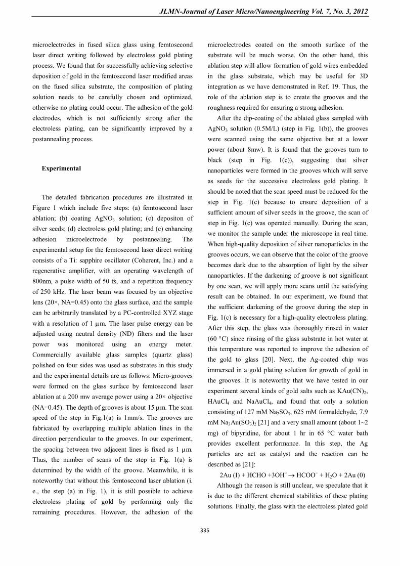
Figure 2 shows an optical micrograph of the top view of a straight gold wire formed on the glass substrate. The width of the wire is about 15 µm. It can be seen that the
groove is fully filled with gold, leading to the uniform and continuous wire.
Fig. 2. Top-view optical micrograph of a gold wire formed on
glass substrate with the width of ~15 µm.
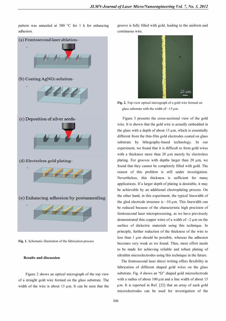
Figure 3 presents the cross-sectional view of the gold wire. It is shown that the gold wire is actually embedded in the glass with a depth of about 15 µm, which is essentially different from the thin-film gold electrodes coated on glass substrate by lithography-based technology. In our experiment, we found that it is difficult to form gold wires with a thickness more than 20 µm merely by electroless plating. For grooves with depths larger than 20 µm, we found that they cannot be completely filled with gold. The reason of this problem is still under investigation. Nevertheless, this thickness is sufficient for many applications. If a larger depth of plating is desirable, it may be achievable by an additional electroplating process. On the other hand, in this experiment, the typical linewidth of the glod electrode structure is ~10 µm. This linewidth can be reduced because of the characteristic high precision of femtosecond laser microprocessing, as we have previously demonstrated thin copper wires of a width of ~2 µm on the surface of dielectric materials using this technique. In principle, further reduction of the thickness of the wire to less than 1 µm should be possible, whereas the adhesion becomes very weak as we found. Thus, more effort needs to be made for achieving reliable and robust plating of ultrathin microelectrodes using this technique in the future.
The femtosecond laser direct writing offers flexibility in fabrication of different shaped gold wires on the glass substrate. Fig. 4 shows an “Ω” shaped gold microelectrode with a radius of about 100 µm and a line width of about 15 µm. It is reported in Ref. [22] that an array of such gold microelectrodes can be used for investigation of the
JLMN-Journal of Laser Micro/Nanoengineering Vol. 7, No. 3, 2012
337
binding ratio of the magnetic beads with the target samples (i.e. leukocytes or gDNA).
Fig. 3. The cross-section of a gold microelectrode,inset picture is
the corresponding gold microelectrode.
Fig.4. The optical micrograph of an “Ω” shaped gold
microelectrode.
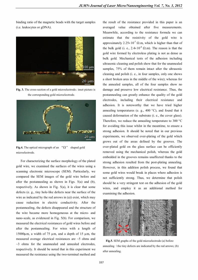
For characterizing the surface morphology of the plated gold wire, we examined the surfaces of the wires using a scanning electronic microscope (SEM). Particularly, we compared the SEM images of the gold wire before and after the postannealing as shown in Figs. 5(a) and (b), respectively. As shown in Fig. 5(a), it is clear that some defects (e. g., tiny hole-like defects near the surface of the wire as indicated by the red arrows in (a)) exist, which may cause reduction in electric conductivity. After the postannealing, the defects disappeared and the structure of the wire became more homogeneous at the micro- and nano-scale, as evidenced in Fig. 5(b). For comparison, we measured the electrical resistances of gold wires before and after the postannealing. For wires with a length of 15000µm, a width of 75 µm, and a depth of 15 µm, the measured average electrical resistances are ~5 ohms and ~3 ohms for the unannealed and annealed electrodes, respectively. It should be noted that in this experiment we measured the resistance using the two-terminal method and
the result of the resistance provided in this paper is an averaged value obtained after five measurements. Meanwhile, according to the resistance formula we can estimate that the resistivity of the gold wire is approximately 2.25×10⁻⁷ Ω.m, which is higher than that of the bulk gold (i. e., 2.4×10⁻⁸ Ω.m). The reason is that the gold wire formed by electroless plating is not as dense as bulk gold. Mechanical tests of the adhesion including ultrasonic cleaning and polish show that for the unannealed samples, 75% of them remain intact after the ultrasonic cleaning and polish (i. e., in four samples, only one shows a short broken area in the middle of the wire); whereas for the annealed samples, all of the four samples show no damage and preserve low electrical resistance. Thus, the postannealing can greatly enhance the quality of the gold electrodes, including their electrical resistance and adhesion. It is noteworthy that we have tried higher annealing temperatures (e. g., 400 °C), and found that it caused deformation of the substrate (i. e., the cover glass). Therefore, we reduce the annealing temperature to 300 °C for avoiding this issue whilst in the meantime, to ensure a strong adhesion. It should be noted that in our previous experiments, we observed over-plating of the gold which grows out of the areas defined by the grooves. The over-plated gold on the glass surface can be efficiently removed using the mechanical polish, whereas the gold embedded in the grooves remains unaffected thanks to the strong adhesion resulted from the post-plating annealing. However, in this addition polish process, we found that some gold wires would break in places where adhesion is not sufficiently strong. Thus, we determine that polish should be a very stringent test on the adhesion of the gold wires, and employ it as an additional method for examining the adhesion.
Fig.5. SEM graphs of the gold microelectrode (a) before
annealing(the tiny defects are indicated by the red arrows; (b)
after annealing.
JLMN-Journal of Laser Micro/Nanoengineering Vol. 7, No. 3, 2012
338
We found that to achieve the high-quality electroless plating of gold in this experiment, the electroless plating solution must be carefully chosen. In fact, we have tried several different kinds of electroless plating solutions, and found that only the solution mentioned above results in formation of high-quality microelectrodes. This might be due to the more stringent requirements on the chemical properties (e. g., PH values) for the other kinds of plating solutions. To clarify this, further investigations are needed. In addition, it is also observed that over-deposition of gold could easily occur, resulting in formation of undesirable gold films on the surface of glass surrounding the embedded microelectrodes. Although this gold film can be easily removed by a mechanical polish, we found that over-deposition can be efficiently suppressed by adding a small amount of bipyridine in the electroless plating, which serves as the stabilizer.
Conclusion
In summary, we have demonstrated the selective electroless plating of conductive gold microelectrode embedded in glass assisted by femtosecond laser modification and post annealing. These metallic wires show good electrical conductivity and strong adhesion. In comparison with conventional techniques, this method is simpler and faster. More importantly, this method is compatible with the current femtosecond laser integration technique, allowing easy integration of gold electrodes with microfluidic reservoirs for biological analysis applications.
This work is supported by National Natural Science Foundation of China (Grant Nos. 60825406, 11104294, 11134010, 10974213 and 61108015) and the Opening Foundation of Key Laboratory of Infrared Imaging Materialand Detectors, Shanghai Institute of Technical Physics, CAS (Grant No. IIMD-KFJJ-10-01).
References
[1] G. M. Whitesides, Nature 442 (2006): 368-373.
[2] H. Craighead, Nature 442 (2006): 387-393.
[3] Y. H. Zheng, Z. N. Zeng, P. Zou, L. Zhang, X. F. Li, P. Liu, R.
X. Li and Z. Z. Xu, Phys. Rev. Lett 103 (2009) 1-4 .
[4] C. Monat, P. Domachuk and B. J. Eggleton, Nat. Photon. 1
(2007): 106-114.
[5] R. Osellame, H. J. W. M. Hoekstra, G. Cerullo and M.
Pollnau,
Laser. Photonics. Rev. 5 (2011): 442-463.
[6] K. Sugioka, and Y. Cheng, Mrs. Bull 36 (2011): 1020-1027.
[7] J. Xu, Y. Liao, H. Zeng, Z. Zhou, H. Sun,J. Song, X. Wang, Y.
Cheng, Z. Z. Xu, K. Sugioka and K. Midorikawa, Opt. Express
15 (2007): 12743-12748.
[8] Y. Liao, J. Xu, Y. Cheng, Z. Z. Xu, K. Sugioka and K.
Midorikawa, J. Laser. Micro. Nanoen 5 (2010): 25-27.
[9] Y. Hanada, K. Sugioka and K. Midorikawa, Appl. Phys. A 90
(2008): 603-607.
[10] K. Hashimoto, K. Ito and Y. Ishimori, Anal. Chem 66
(1994):3830-3833.
[11] J. L.Yan, Y. Du, J. F. Liu, W. D. Cao, S. H. Sun, W. H.
Zhou, X. R. Yang and E. K. Wang, Anal. Chem. 75 (2003):
5406-5412.
[12] A. Michota, and J. Bukowska, J. Raman. Spectrosc. 34
(2003):21-25.
[13] Z. H. Zhou, J. Xu, Y. Cheng, Z. Z. Xu, K. Sugioka and K.
Midorikawa, Jpn. J. Appl. Phys. 47 (2008) 189-192.
[14] J. M. Blakely and J. Appl. Phys. 35 (1964): 1756.
[15] T. A. Green and Gold. Bull 40 (2007): 105-114.
[16] Y. Yasutake, K. Kono, M. Kanehara, T. Teranishi, M. R.
Buitelaar, C. G. Smith and Y. Majima, Appl. Phys. Lett 91 (2007):
203107.
[17] K. Sugioka and K. Toyoda, Appl. Phys. A 54 (1992):
380-383.
[18] Q. H. Zhou, H. W.Chen and Y. Wang, Electrochim. Acta 55
(2010): 2542-2549.
[19] Y. Liao, J. Xu, Y. Cheng, Z. H. Zhou, F. He, H. Y. Sun, X. S.
Wang, Z. Z. Xu, K. Sugioka and K. Midorikawa, Opt. Lett 33
(2008), 2281-2283.
[20] V. P. Menon and C. R. Martin, Anal. Chem. 67 (1995), 1920
-1928.
[21] A. Hilmi and H. T. John Luong Anal. Chem. 72 (2000),
4677-4682.
[22] K. Y. Lien, C. J. Liu, Y. C. Lin, P. L. Kuo and G. B. Lee, Microfluid. Nanofluid. 6 (2009): 539-555.
(Received: April 16, 2012, Accepted: August 08, 2012)