Fabrication of computer generated holograms using hot ...
5
A. Rojek, A. Kowalik, J. Podgórski mATERiAłY ElEKTRoNiczNE (Electronic Materials), 2018, 46, 1 - 4 3 The article presents the investigation to develop a technology for fabricating micro-and nanostructures of a high dimen- sional precision using the processes of Hot Embossing Nano Imprint Lithography. The research was carried out for three thermoplastic polymers, i.e. poly(methyl methacrylate), olefin copolymer and polycarbonate in order. The process parameters and pattern correction coefficients for shrinkage compensation have been determined. The accuracy better than 1.25 x 10 -3 % has been reached for the pattern replicated onto olefin copolymer substrates. Key words: Hot Embossing Nano Imprint Lithography, nanoimprint, computer generated holograms Technologia wytwarzania replik hologramów syntetycznych w procesach tłoczenia na gorąco W artykule przedstawiono technologię wytwarzania kopii (replik) mikro- i nanostruktur o dużej precyzji wymiarowej w procesach tłoczenia na gorąco (Hot Embossing Nano Imprint Lithography). Badania prowadzono dla trzech polimerów termoplastycznych - polimetakrylanu metylu, kopolimeru olefinowego oraz poliwęglanu. określono warunki procesów i współczynniki korekty wzorów kompensujące skurcz towarzyszący kopiowaniu struktur. Uzyskano repliki, dla których względny błąd wymiarów poprzecznych wynosił poniżej 1,25 x 10 -3 %. Słowa kluczowe: tłoczenie na gorąco, nanoimprint, hologramy syntetyczne Fabrication of computer generated holograms using hot embossing nano imprint lithography open access Anna Rojek 1 , Andrzej Kowalik 1 , Jarosław Podgórski 1 1 Institute of Electronic Materials Technology, 133 Wólczyńska str., 01-919 Warsaw, Poland e-mail: [email protected] 1. Introduction The microlithographic process based on hot embos- sing of thermoplastic materials (called Hot Embossing Nano Imprint Lithography - HE NIL) is an efficient and simple technology of the fabrication of 3D structures with the submicron elements. This process was classified by International Technology Roadmap for Semiconductors (ITRS, www.itrs.net) as one of the new lithographic me- thods referred to as Next Generation Lithography (NGL), expected to enable manufacturing structures of a size even below 32 nm. A technology with such a resolution can thus be successfully applied to produce the replicas of the structures whose fabrication requires the use of the most advanced and very expensive microlithographic methods, i.e. the electron-beam pattern generation or EUV projection printing. HE NIL is being increasingly used for the production of micro-opto-electro-mechanical elements and systems (MOEMS). The examples can be microflow devices (Lab- -on-chip) [1 - 2], micro-lenses, the structures improving brightness of the LCD screens [3] and computer-generated holograms [4]. In the HE NIL process, a pattern is transferred onto a thermoplastic polymer substrate heated to a temperature exceeding glass transition temperature (T g ), using a ma- ster stamp with a given contact force. After cooling the stamp/substrate system to a temperature below T g and detachment, the replicated pattern is preserved in the polymer. However, obtaining high quality replicas, especially in the case of the large surface area microstructures (a few to several dozen cm 2 ), requires a very careful selection of the process conditions, primarily the temperature and pressure force during embossing and the temperature of detachment. The too high value of the embossing tempe- rature will cause large deformations of the substrate, while the too low value will result in a loss of the fidelity of the replicated relief (a relief too shallow, large distortion of small elements). Similarly, the temperature which gets too high during de-embossing may be the reason for the pattern deformation, while temperature that is too low may cause the destruction of the stamp and the substrate due to the stresses induced by the large differences in their thermal expansion coefficients [5 - 9]. A separate problem refers to the significant changes in the size of the replicas with respect to the original. The accurate thermal shrinkage compensation is par- ticularly important in the case of synthetic holograms (computer generated diffractive optical structures, whose operation is based on the light diffraction). The dimensio- nal accuracy of such elements should be comparable with the wavelength of the light, for which they are designed. Otherwise, it could lead to a significant deterioration of the quality of the wave front formed by the element.
Transcript of Fabrication of computer generated holograms using hot ...
A. Rojek, A. Kowalik, J. Podgórski
mATERiAłY ElEKTRoNiczNE (Electronic Materials), 2018, 46, 1 - 4 3
The article presents the investigation to develop a technology for fabricating micro-and nanostructures of a high dimen-sional precision using the processes of Hot Embossing Nano Imprint Lithography. The research was carried out for three thermoplastic polymers, i.e. poly(methyl methacrylate), olefin copolymer and polycarbonate in order. The process parameters and pattern correction coefficients for shrinkage compensation have been determined. The accuracy better than 1.25 x 10⁻³ %has been reached for the pattern replicated onto olefin copolymer substrates.
Key words: Hot Embossing Nano Imprint Lithography, nanoimprint, computer generated holograms
technologia wytwarzania replik hologramów syntetycznych w procesach tłoczenia na gorącoW artykule przedstawiono technologię wytwarzania kopii (replik) mikro- i nanostruktur o dużej precyzji wymiarowej w procesach tłoczenia na gorąco (Hot Embossing Nano Imprint Lithography). Badania prowadzono dla trzech polimerów termoplastycznych - polimetakrylanu metylu, kopolimeru olefinowego oraz poliwęglanu. określono warunki procesów i współczynniki korekty wzorów kompensujące skurcz towarzyszący kopiowaniu struktur. Uzyskano repliki, dla których względny błąd wymiarów poprzecznych wynosił poniżej 1,25 x 10⁻³ %.
Słowa kluczowe: tłoczenie na gorąco, nanoimprint, hologramy syntetyczne
Fabrication of computer generated holograms usinghot embossing nano imprint lithography
open access
Anna Rojek1, Andrzej Kowalik1, Jarosław Podgórski1
1 Institute of Electronic Materials Technology, 133 Wólczyńska str., 01-919 Warsaw, Poland e-mail: [email protected]
1. Introduction
The microlithographic process based on hot embos-sing of thermoplastic materials (called Hot Embossing Nano Imprint Lithography - HE NIL) is an efficient and simple technology of the fabrication of 3D structures with the submicron elements. This process was classified by International Technology Roadmap for Semiconductors (ITRS, www.itrs.net) as one of the new lithographic me-thods referred to as Next Generation Lithography (NGL), expected to enable manufacturing structures of a size even below 32 nm. A technology with such a resolution can thus be successfully applied to produce the replicas of the structures whose fabrication requires the use of the most advanced and very expensive microlithographic methods, i.e. the electron-beam pattern generation or EUV projection printing.
HE NIL is being increasingly used for the production of micro-opto-electro-mechanical elements and systems (MOEMS). The examples can be microflow devices (Lab--on-chip) [1 - 2], micro-lenses, the structures improving brightness of the LCD screens [3] and computer-generated holograms [4].
In the HE NIL process, a pattern is transferred onto a thermoplastic polymer substrate heated to a temperature exceeding glass transition temperature (Tg), using a ma-ster stamp with a given contact force. After cooling the
stamp/substrate system to a temperature below Tg and detachment, the replicated pattern is preserved in the polymer.
However, obtaining high quality replicas, especially in the case of the large surface area microstructures (a few to several dozen cm2), requires a very careful selection of the process conditions, primarily the temperature and pressure force during embossing and the temperature of detachment. The too high value of the embossing tempe-rature will cause large deformations of the substrate, while the too low value will result in a loss of the fidelity of the replicated relief (a relief too shallow, large distortion of small elements). Similarly, the temperature which gets too high during de-embossing may be the reason for the pattern deformation, while temperature that is too low may cause the destruction of the stamp and the substrate due to the stresses induced by the large differences in their thermal expansion coefficients [5 - 9].
A separate problem refers to the significant changes in the size of the replicas with respect to the original. The accurate thermal shrinkage compensation is par-ticularly important in the case of synthetic holograms (computer generated diffractive optical structures, whose operation is based on the light diffraction). The dimensio-nal accuracy of such elements should be comparable with the wavelength of the light, for which they are designed. Otherwise, it could lead to a significant deterioration of the quality of the wave front formed by the element.

Fabrication of computer generated holograms using hot embossing ...
4 mATERiAłY ElEKTRoNiczNE (Electronic Materials), 2018, 46, 1 - 4
For instance, for one of the basic diffractive optical elements, i.e. a diffractive lens, the lack of proper com-pensation will cause a change in the focal length and aberrations, which will result in a deformation of the focus. The obtained element will be characterized not only by the altered basic parameter (focal length), but also by a much worse quality (high spherical aberration).
In this paper we report on the research oriented to-wards the development of the fabrication processes (part 2) and the compensation of shrinkage (part 3) in the HE NIL processes for the three most commonly used thermopla-stic polymers. Part 4 presents the results of the applied solutions for fabricating COC replicas. Part 5 contains a summary of the research.
2. Manufacturing process
The investigations were carried out for the three most common types of polymer substrates, namely: poly(methyl methacrylate) - PMMA, olefin copolymer - COC and poly-carbonate - PC. For the replicating processes we used the HE NIL EVG510 nanoimprint system. That device enables replicas on the substrates of a diameter up to 100 mm. The embossing process takes place in the vacuum cham-ber (pressure ≤ 2 mbar), which prevents air trapping in the relief being produced. The maximum pressure force is 10 kN and it is controlled with an accuracy of ± 3%. The system allows the independent control of the heating of the substrate and the stamp for the temperature up to 550°C (heaters and temperature sensors placed in the base and in the piston; the control with an accuracy of ± 2%). A single-sided cooling system located in the base was used to controll cooling of the bottom plate. In the HE NIL processes a soft stamp was used, i.e. a stamp with a relief made in a polymer layer (a Fluorolink MD700 photo-polymer, thickness 150 - 250 μm), applied onto a glass
substrate. A stamp like this, especially in the case of the structures with a large surface area, has two important advantages, namely:
1) it provides much better contact with the substrate than hard stamps (micro-waviness smoothing),
2) it makes the detachment process of replica from the stamp easier.
For the fabrication of a soft stamp we used a master stamp made in a process of electron-beam lithography (Vistec SB251), that guaranteed the accuracy of the posi-tion of the pattern elements at the level of 10 nm.
For each of the selected polymers, technological tests were carried out, in which the values of contact force were changed in the range of 5 - 8 kN, the temperature during embossing was in the range 15 - 25°C above Tg, and temperature during separation was in the range 5 - 15°C below Tg.
The maximum possible heating rate of the system was assumed as 10°/min, and a much lower cooling rate of 2°/min, which allowed precise control of the tempe-rature distribution of the stamp-substrate system prior to the separation process and thus ensured high process reproducibility. The parameters of the processes that were considered optimal, based on inspection of replicas using the optical and electron microscopes, are presented in Tab. 1.
Fig.1 shows the replicas of the eight- and four--phase-level diffractive lenses as the examples of the structures made on the basis of the optimized process. The examination of their optical properties revealed that the replicas do not deviate in quality from the originals, with the diffraction efficiency of the replicated lenses equ-al to 0.99 ± 0.01 with respect to the originals in the case of the eight-level profiles, and to 1.00 ± 0.01 in the case of the four-level profiles (the measured efficiency diffe-rences were within the margin of the measurement error).
process parametersreplica material
PMMA COC PC
copying
heating rate [0C/min] 10 10 10
temperature [0C] 125 150 170
contact force [N] 7000 7000 7000
contact time [min] 1 1 1
separationcooling rate [0C/min] 2 2 2
temperature [0C] 90 120 138
Tab. 1. The parameters of the HE NIL processes for the selected polymer substrates.Tab. 1. Parametry procesów HE NIL dla wybranych podłoży polimerowych.

A. Rojek, A. Kowalik, J. Podgórski
mATERiAłY ElEKTRoNiczNE (Electronic Materials), 2018, 46, 1 - 4 5
Fig. 1. Images of the central part of the four- and eight -phase-level diffractive lenses (top and bottom, respectively) (Veeco Contour GTK 1 optical profilometer): on the left – a quartz original, on the right – a replica on COC substrate.Rys. 1. Obrazy soczewek dyfrakcyjnych o czterech (u góry) i ośmiu (u dołu) poziomach fazowych (profilometr optyczny Veeco Contour GTK 1): z lewej – oryginał kwarcowy, z prawej – repliki na podłożu COC.
3. shrinkage compensation
High temperatures of the copying process (120° - 170°C) and large differences between the values of thermal expansion coefficient of the materials of the stamp (glass, 3 x 10⁻⁶) and the replica (polymer, 60 x 10-6 - 70 x 10-6)
result in the dimensions of the copied structures being significantly different from the dimensions of the stamp. However, provided that we know the shrinkage accompa-nying the copying process, we can eliminate these errors by fabricating a stamp with a properly enlarged pattern. Taking into account the fundamental dependence:
δ = c x ΔT,
where δ - shrinkage, c - linear expansion coefficient, ΔT - temperature difference, the theoretical value of the replica shrinkage can be determined on the basis of the thermal expansion coefficients of the materials of the substrate cR, and the stamp cS, using the dependence:
δRteoret = cR (Tg – T0) [1 + cS (Tg – T0)],
where: Tg – glass transition temperature, assumed as the temperature value during replication, T0 - ambient tem-perature, cS
(Tg – T0) – a term expressing the change in the dimension of the stamp at the embossing temperature.
However, if we take into account that the transition
(1)
(2)
temperature of a polymer from a plastic state to a fully elastic state is not clearly defined (it is rather a certain range within the glass transition temperature range, Tg), it can be assumed from the outset that the theoreti-cal method will be erroneous. We decided that the experimental determination of the shrinkage, and the shrinkage-based determination of the correction factors necessary for the shrinkage compensation, should provide much more accurate dimensions of the replicas.
The measurements were taken for each of the tested materials for two replicas with a test pattern of 50 x 50 mm2, consisting of an array of 5 x 5 markers that were placed every 10 mm. The measurements were do-ne using electron-beam lithography system Vistec SB251. The system allows for the use of an electron beam to scan a selected area of the substrate (si-milarly to an electron scanning microscope) and to determine the position of the selected topological element (a marker) with an accuracy up to 10 nm. In practice, due to the scanning limitations of the polymer substrate (charging effects, polymer destruction due to the exposition of a high energy beam), the accuracy of the method is much lower, at the level of 0.5 μm. Howe-ver, such an accuracy can be considered sufficient, because the relative error of the shrinkage measurement would be 5 x 10⁻⁵ and 1 x 10⁻⁵ regarding a distance between the ad-jacent markers and the most distant markers, respectively.
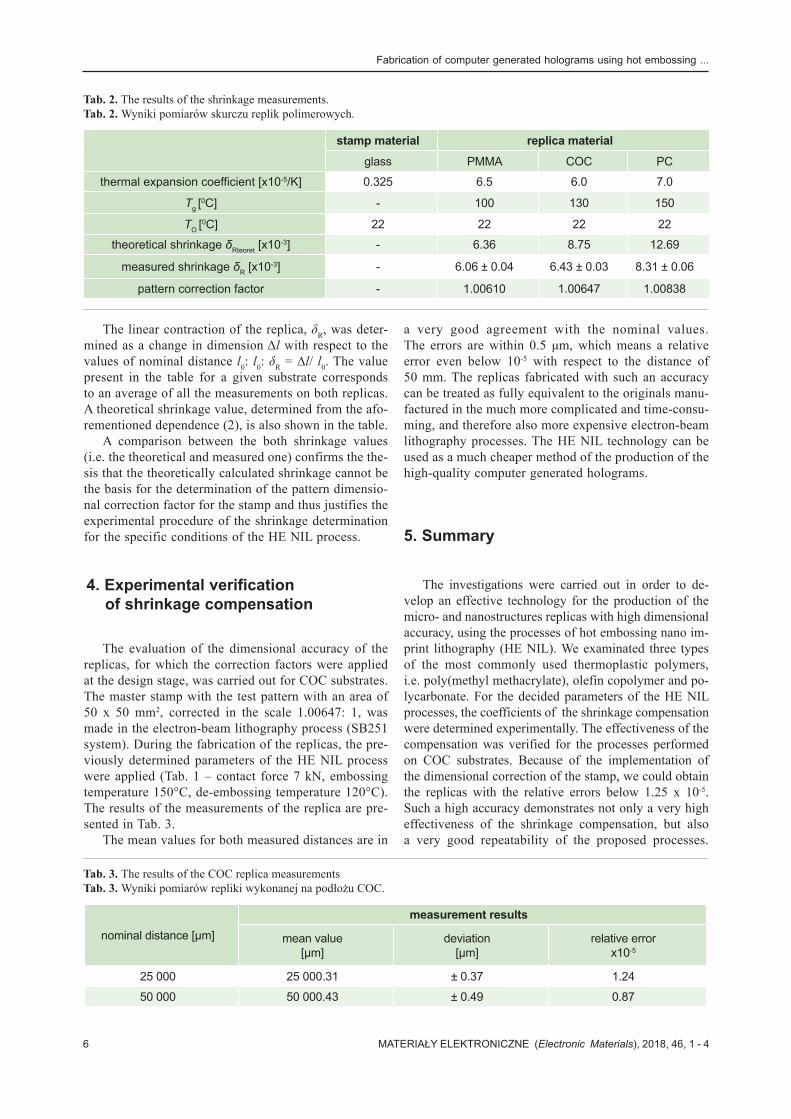
The shrinkage values, determined experimentally, are shown in Tab. 2.
Fabrication of computer generated holograms using hot embossing ...
6 mATERiAłY ElEKTRoNiczNE (Electronic Materials), 2018, 46, 1 - 4
The linear contraction of the replica, δR, was deter-mined as a change in dimension Δl with respect to the values of nominal distance l0: l0: δR = ∆l/ l0. The value present in the table for a given substrate corresponds to an average of all the measurements on both replicas. A theoretical shrinkage value, determined from the afo-rementioned dependence (2), is also shown in the table.
A comparison between the both shrinkage values (i.e. the theoretical and measured one) confirms the the-sis that the theoretically calculated shrinkage cannot be the basis for the determination of the pattern dimensio-nal correction factor for the stamp and thus justifies the experimental procedure of the shrinkage determination for the specific conditions of the HE NIL process.
4. experimental verification of shrinkage compensation
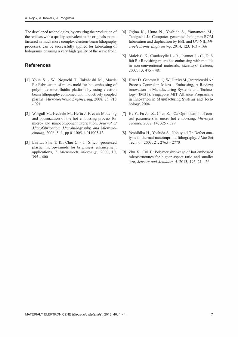
The evaluation of the dimensional accuracy of the replicas, for which the correction factors were applied at the design stage, was carried out for COC substrates. The master stamp with the test pattern with an area of 50 x 50 mm2, corrected in the scale 1.00647: 1, was made in the electron-beam lithography process (SB251 system). During the fabrication of the replicas, the pre-viously determined parameters of the HE NIL process were applied (Tab. 1 – contact force 7 kN, embossing temperature 150°C, de-embossing temperature 120°C). The results of the measurements of the replica are pre-sented in Tab. 3.
The mean values for both measured distances are in
Tab. 2. The results of the shrinkage measurements.Tab. 2. Wyniki pomiarów skurczu replik polimerowych.
stamp material replica materialglass PMMA COC PC
thermal expansion coefficient [x10-5/K] 0.325 6.5 6.0 7.0
Tg [0C] - 100 130 150
TO [0C] 22 22 22 22theoretical shrinkage δRteoret [x10-3] - 6.36 8.75 12.69
measured shrinkage δR [x10-3] - 6.06 ± 0.04 6.43 ± 0.03 8.31 ± 0.06
pattern correction factor - 1.00610 1.00647 1.00838
a very good agreement with the nominal values. The errors are within 0.5 μm, which means a relative error even below 10-5 with respect to the distance of 50 mm. The replicas fabricated with such an accuracy can be treated as fully equivalent to the originals manu-factured in the much more complicated and time-consu-ming, and therefore also more expensive electron-beam lithography processes. The HE NIL technology can be used as a much cheaper method of the production of the high-quality computer generated holograms.
5. summary
The investigations were carried out in order to de-velop an effective technology for the production of the micro- and nanostructures replicas with high dimensional accuracy, using the processes of hot embossing nano im-print lithography (HE NIL). We examinated three types of the most commonly used thermoplastic polymers, i.e. poly(methyl methacrylate), olefin copolymer and po-lycarbonate. For the decided parameters of the HE NIL processes, the coefficients of the shrinkage compensation were determined experimentally. The effectiveness of the compensation was verified for the processes performed on COC substrates. Because of the implementation of the dimensional correction of the stamp, we could obtain the replicas with the relative errors below 1.25 x 10⁻⁵. Such a high accuracy demonstrates not only a very high effectiveness of the shrinkage compensation, but also a very good repeatability of the proposed processes.
Tab. 3. The results of the COC replica measurementsTab. 3. Wyniki pomiarów repliki wykonanej na podłożu COC.
nominal distance [µm]
measurement results
mean value [µm]
deviation [µm]
relative error x10-5
25 000 25 000.31 ± 0.37 1.2450 000 50 000.43 ± 0.49 0.87
A. Rojek, A. Kowalik, J. Podgórski
mATERiAłY ElEKTRoNiczNE (Electronic Materials), 2018, 46, 1 - 4 7
The developed technologies, by ensuring the production of the replicas with a quality equivalent to the originals manu-factured in much more complex electron-beam lithography processes, can be successfully applied for fabricating of holograms ensuring a very high quality of the wave front.
References
[1] Youn S. - W., Noguchi T., Takahashi M., Maeda R.: Fabrication of micro mold for hot-embossing of polyimide microfluidic platform by using electron beam lithography combined with inductively coupled plasma, Microelectronic Engineering, 2008, 85, 918 - 921
[2] Worgull M., Heckele M., He´tu J. F. et al: Modeling and optimization of the hot embossing process for micro- and nanocomponent fabrication, Journal of Microfabrication, Microlithography, and Microma-chining, 2006, 5, 1, pp.011005-1-011005-13
[3] Lin L., Shia T. K., Chiu C. - J.: Silicon-processed plastic micropyramids for brightness enhancement applications, J. Micromech. Microeng., 2000, 10, 395 - 400
[4] Ogino K., Unno N., Yoshida S., Yamamoto M., Taniguchi J.: Computer generated hologram-ROM fabrication and duplication by EBL and UV-NIL,Mi-croelectronic Engineering, 2014, 123, 163 - 166
[5] Malek C. K., Coudevylle J. - R., Jeannot J. - C., Duf-fait R.: Revisiting micro hot-embossing with moulds in non-conventional materials, Microsyst Technol, 2007, 13, 475 - 481
[6] Hardt D., Ganesan B., Qi W., Dirckx M., Rzepniewski A.: Process Control in Micro - Embossing, A Review; innovation in Manufacturing Systems and Techno-logy (IMST), Singapore MIT Alliance Programme in Innovation in Manufacturing Systems and Tech-nology, 2004
[7] He Y., Fu J. - Z., Chen Z. - C.: Optimization of con-trol parameters in micro hot embossing, Microsyst Technol, 2008, 14, 325 - 329
[8] Yoshihiko H., Yoshida S., Nobuyuki T.: Defect ana-lysis in thermal nanoimprintu lithography. J Vac Sci Technol, 2003, 21, 2765 - 2770
[9] Zhu X., Cui T.: Polymer shrinkage of hot embossed microstructures for higher aspect ratio and smaller size, Sensors and Actuators A, 2013, 195, 21 - 26


![Computer generated hologram from full-parallax 3D image data …cvlab.khu.ac.kr/paper43.pdf · 2015. 5. 26. · using computer generated holograms (CGH)[5]. Another approach for computational](https://static.fdocuments.net/doc/165x107/60fd680706a560061e59c5f3/computer-generated-hologram-from-full-parallax-3d-image-data-cvlabkhuackr-.jpg)