Fabrication of CLIC X-band RF structures and RF components
26
[email protected] 21-Oct-2010 Holland@CERN Fabrication of CLIC X-band RF structures and RF components G. Riddone OUTLINE ° Two-beam module ° RF accelerating structures ° Power extraction and transfer structures ° RF components
Transcript of Fabrication of CLIC X-band RF structures and RF components

10-Nov-2010 1 Holland@CERN21-Oct-2010 Holland@CERN
Fabrication of CLIC X-bandRF structures and RF components
G. Riddone
OUTLINE° Two-beam module ° RF accelerating structures° Power extraction and transfer structures° RF components

10-Nov-2010 2 Holland@CERN
MAIN LINAC – TWO-BEAM MODULE
CLIC at 500 GeV (4248 modules)26312 Accelerating structures13156 PETS~ 70000 RF components
CLIC at 3 TeV (20924 modules)142812 Accelerating structures71406 PETS~ 400000 RF components
A. Samoshkin
(POWER EXTRACTION AND TRANSFER SYSTEM)
MAIN BEAM
DRIVE BEAM
Up to 8 accelerating structures and 4 PETS in a two-beam module
Prototype modules (20) 2016Few 100’s RF structures and components

10-Nov-2010 3 Holland@CERN
RF STRUCTURES AND COMPONENTS
3
TD18#3 at SLAC
TD18#2 at KEK
TD24#2 at CERN (12 GHz)
PETS (12 GHz, TBTS)
PETS (11.4 GHz, test at SLAC)High-power dry load Hybrid
Variable high power splitter

10-Nov-2010 5 Holland@CERN
Test structures
CLIC accelerating structures
DisksCouplersCooling circuits
DisksCouplersCooling circuits [~400 W average per structure]Vacuum manifolds (10-9 mbar)Damping materialSuperstructures (2 to 4)
ACCELERATING STRUCTURES
L ~300 mm
L = 500 mm
10-Nov-2010 6 Holland@CERN
ENGINEERING DESIGN ISSUES (WAVEGUIDE DAMPED AS)
Iris
12WDSDVG1.8_R05
0.005 A B
Geometrical tolerance of this zone
// 0.002 A
0.001
PREP
ARE
D B
Y A
. SO
LOD
KO

10-Nov-2010 7 Holland@CERN
CLIC’s needs: shape accuracy ± 2.5 µmroughness Ra 25 nm
S. ATIEH
WHY WE NEED ULTRA-PRECISION MACHINING
Accelerating structures– Milling and turning
PETS– Milling
Diamond tool is required (about 7 tools per disks)
- Dimensional stability
- Maintenance of tolerances
- Less stresses
- Chips do not adhere to surface
- Expensive → well characterised
At this level of tolerances: material stress-relief annealing is mandatory → Soft material → • Special care clamping without damage• Special requirements on 3D metrology (tactile): no indents!!

10-Nov-2010 8 Holland@CERN
TYPICAL PROCEDURE OF UHP DISKMACHINING
Pre-Fabrication:Pre-turning + x100 μmPre-milling + x100 μmTuning holesStress relief ~180 °C (optional)Finish turning + x10μmFinish milling + x10μmStress relief ~245 °C
UHP-Machining:Mounting of vacuum clamping adapterUHP-turning of the support (diamond tools)AlignmentUHP-turning ref. plan A AlignmentUHP-turning opposite sideWave guide UHP millingIris final turning (requested up to the nose)
S. ATIEH

10-Nov-2010 9 Holland@CERN
DETUNED DAMPED DISK FROM VDL (TD24)
Zeiss CMM, free state measurement
• Shape accuracy 5 µm 2.6 µm achieved
• Roughness Ra 0.025Iris region achieved Ra 0.016

10-Nov-2010 10 Holland@CERN
ASSEMBLY PROCEDURE
Diamond machining (sealed structures)
H2 diffusion bonding/brazing at
~ 1000 ˚C
Surface treatment -cleaning with light etch
Vacuum baking650 ˚C > 10 days

10-Nov-2010 11 Holland@CERN
ALIGNMENT AND BONDING Reference on the external diameter: - tolerance on external diameter: 12.5 µm- tolerance on the ref. line: 1 µmAlignment done on a V-shape vertical support in granite (accuracy of 1.5 µm)
Operation done under laminar flow
Straightness measurementT24: 3.5 µm
Individual inspection

10-Nov-2010 12 Holland@CERN
DIFFUSION BONDING PARAMETERS AND CYCLE
Temperature: up to 1040 ˚CPressure: 0.28 MPaHolding time: 2 h
Nominal diffusion bonding cycle (under 25 mbar H2)
New infrastructure to guarantee uniform load
Straightness measurement after diffusion bonding: variation of 1 µm before and after bonding

10-Nov-2010 13 Holland@CERN
MACHINING AND DIFFUSION BONDING ISSUES
MILLINGTURNING
GRAINS CROSSING THE JOINING PLANE
VACUUM
DIFFUSION BONDING (H2 better surface)
MACHINING (as much turning as possible!)
H2 (no faceting!)

10-Nov-2010 14 Holland@CERN
1. Diffusion bonding of highprecision disk stack
2. Brazing of the manifolds by means of Gold-electroplating (validation tests needed)
3. Brazing of cooling fitting adapters
RF INTERFACE FLANGE
COOLING FITTING ADAPTER
MANIFOLD BODY
WFM WAVEGUIDE
WAVEGUIDE
ACCELERATINGSTRUCTURE
GOLD-ELECTROPLATING
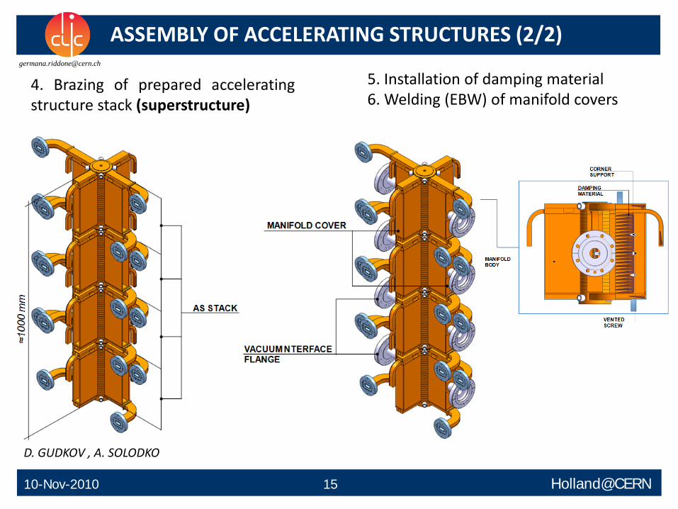
ASSEMBLY OF ACCELERATING STRUCTURES (1/2)
D. GUDKOV, A. SOLODKO
10-Nov-2010 15 Holland@CERN
4. Brazing of prepared acceleratingstructure stack (superstructure)
5. Installation of damping material6. Welding (EBW) of manifold covers
ASSEMBLY OF ACCELERATING STRUCTURES (2/2)
D. GUDKOV , A. SOLODKO

10-Nov-2010 17 Holland@CERN
FABRICATION OF PETS AT 11.4 GHz
PETS for feasibility demonstration- successfully tested at SLAC
Coupler
Minitank with bars inside

10-Nov-2010 20 Holland@CERN
PETS OCTANT FOR TEST BEAM LINE
• Shape accuracy 4.8 µm (15 µm nominal)
• Roughness Ra 120 -180 nm(100 nm nominal)
KERN Micro- und Feinwerktechnik GmbH (DE)
L = 800 mm

10-Nov-2010 21 Holland@CERN
RF COMPONENTSCurrent needs for CERN and several collaborators

10-Nov-2010 22 Holland@CERN
HIGH POWER DRY LOADS
Internal shape
Broadband: 11.4 GHz and 12 GHz (design made by CERN)
Ferritic stainless steel SS430ripple shape tolerance = 0.01 mmflatness accuracy 0.01 mmripple shape roughness Ra 0.4.
RF measurements-28.5 dB 11.424 GHz -36.3 dB 11.994 GHzDesign (HFSS): -39.5 dB 11.424 GHz
-30.7 db 11.992 GHz
Successfully tested at high power at KEK
L ~ 0.8 m

10-Nov-2010 23 Holland@CERN
HIGH POWER COMPACT DRY LOADS
Water cooled load
Ceramic (SiC) - 3 mm Cu coating needed
Cu OFE body brazed to the RF flanges and to SiC inner part
L ~ 0.3 m
V. SOLDATOV

10-Nov-2010 24 Holland@CERN
OTHER RF COMPONENTS
Hybrids Splitter RF flanges and waveguides
Directional couplers
Phase shifter
Variable Power AttenuatorDesign made by the company
Design made by CERN

10-Nov-2010 25 Holland@CERN
CLIC TENTATIVE SCHEDULE
Final CLIC CDR andproposal next phase
@ CERN Council
European Strategyfor Particle Physics
@ CERN Council
Project Implementation Plan (PIP) andproposal for next phase
Draft ConceptualDesign Report (CDR)
2010 2011 2012 2013 2014 2015 2016 2017 2018
Feasibility issues (Accelerator&Detector) Conceptual design & preliminary cost estimationEngineering, industrialisation & cost optimisation ?Project Preparation Project Implementation ?
JP. Delahaye

10-Nov-2010 26 Holland@CERN
• Future needs for RF structures and RF components are increasing:– Conceptual design phase will be followed by a technical design phase
from 2011 to 2016 (project preparation)
• Production of RF accelerating structures and PETS is very challenging: for future CLIC structures all technical systems will have to be integrated
• Micro-precision tolerances imply dedicated machining and assembly procedures: qualification of firms for fully equipped RF structures and components is mandatory
• Industrialization studies need to be conducted with companies
CONCLUSIONS