Fabrication of Antenna-coupled Bolometers with Al/Ti/Au...
17
Fabrication of Antenna-coupled Bolometers with Al/Ti/Au TES Readouts Minhee Yun, James Bock, Henry Leduc, and Peter Day Jet Propulsion Laboratory, California Institute of Technology California Institute of Technology California Institute of Technology July 10, 2003 Moon Kim Department of Material Science and Engineering, University of North Texas
Transcript of Fabrication of Antenna-coupled Bolometers with Al/Ti/Au...

Fabrication of Antenna-coupled Bolometers with Al/Ti/Au TES Readouts
Minhee Yun, James Bock, Henry Leduc, and Peter DayJet Propulsion Laboratory, California Institute of Technology
California Institute of TechnologyCalifornia Institute of Technology
July 10, 2003
Moon KimDepartment of Material Science and Engineering,
University of North Texas

2
California Institute of TechnologyCalifornia Institute of Technology
LTD 10, Genoa, Italy
Photon Noise and Thermal Reserve
NEPbol = γ γ γ γ [[[[4kT2G]1/2
Qmax = ∫∫∫∫ G(T’)dT’ = S Q0
NEPbol = f [16kT0SQ0]1/2
NEPphoton = [2hννννQ0(1+εηεηεηεη/(ex-1)]1/2
Example:Photons from CMB onlyηηηηopt = 50 %, ∆ν∆ν∆ν∆ν/νννν = 30 %TES bolometer with S = 5
NTD Ge bolometers have Johnson noise,but more dynamic range due to rebiasingSlightly better for this optimization
No bunching term
With bunching term
3
California Institute of TechnologyCalifornia Institute of Technology
LTD 10, Genoa, Italy
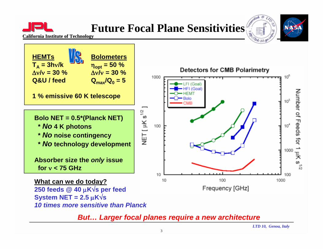
Future Focal Plane Sensitivities
HEMTs BolometersTA = 3hνννν/k ηηηηopt = 50 %∆ν∆ν∆ν∆ν/νννν = 30 % ∆ν∆ν∆ν∆ν/νννν = 30 %Q&U / feed Qmax/Q0 = 5
1 % emissive 60 K telescope
Bolo NET = 0.5*(Planck NET)* No 4 K photons* No noise contingency* No technology development
Absorber size the only issuefor νννν < 75 GHz
What can we do today?250 feeds @ 40 µµµµK√√√√s per feedSystem NET = 2.5 µµµµK√√√√s10 times more sensitive than Planck
But… Larger focal planes require a new architecture
Future Focal Plane Sensitivities
4
California Institute of TechnologyCalifornia Institute of Technology
LTD 10, Genoa, Italy
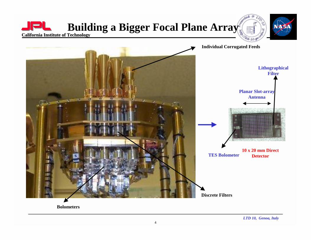
Building a Bigger Focal Plane Array
10 x 20 mm Direct Detector
Individual Corrugated Feeds
Discrete Filters
Bolometers
Lithographical Filter
Planar Slot-array Antenna
TES Bolometer

5
California Institute of TechnologyCalifornia Institute of Technology
LTD 10, Genoa, Italy
See Griffin, Bock & GearApplied Optics 2002Astro-ph 0205264
Directed Beams for Mm-wave Systems
R = ννννIνννν(instrument) / ννννIνννν(sky)
Obs
ervi
ng s
peed
ratio
Background-limited filled array vs. 2fλλλλ feedhorn array:
• ~3x better mapping speed• 16 times more detectors• Simpler operating modes• Requires straylight control
Millimeter-wave case:
• Sky is 2.7 K• Need extreme control of beams
even in a 2 K environment• Sub-K re-imaging optics? Or• Directed beams
~N1/3 improvement
6
California Institute of TechnologyCalifornia Institute of Technology
LTD 10, Genoa, Italy
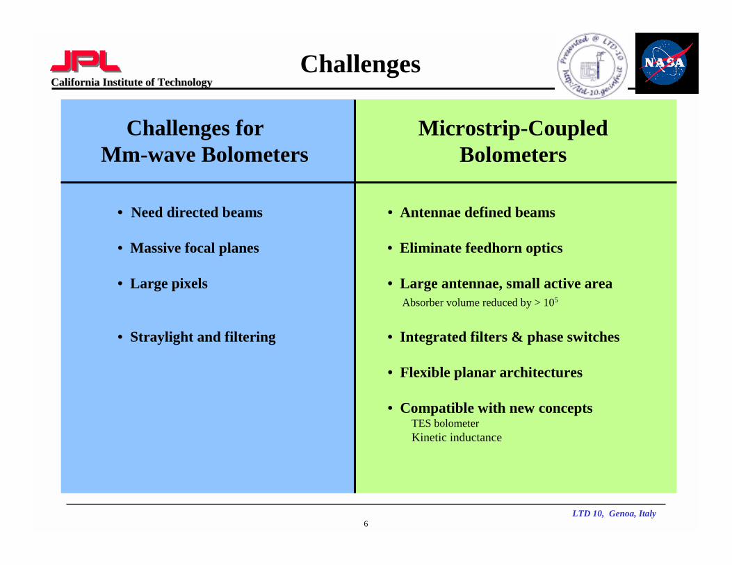
Challenges
Challenges forMm-wave Bolometers
• Need directed beams • Antennae defined beams
• Massive focal planes • Eliminate feedhorn optics
• Large pixels • Large antennae, small active areaAbsorber volume reduced by > 105
• Straylight and filtering • Integrated filters & phase switches
• Flexible planar architectures
• Compatible with new conceptsTES bolometerKinetic inductance
Microstrip-CoupledBolometers
7
California Institute of TechnologyCalifornia Institute of Technology
LTD 10, Genoa, Italy
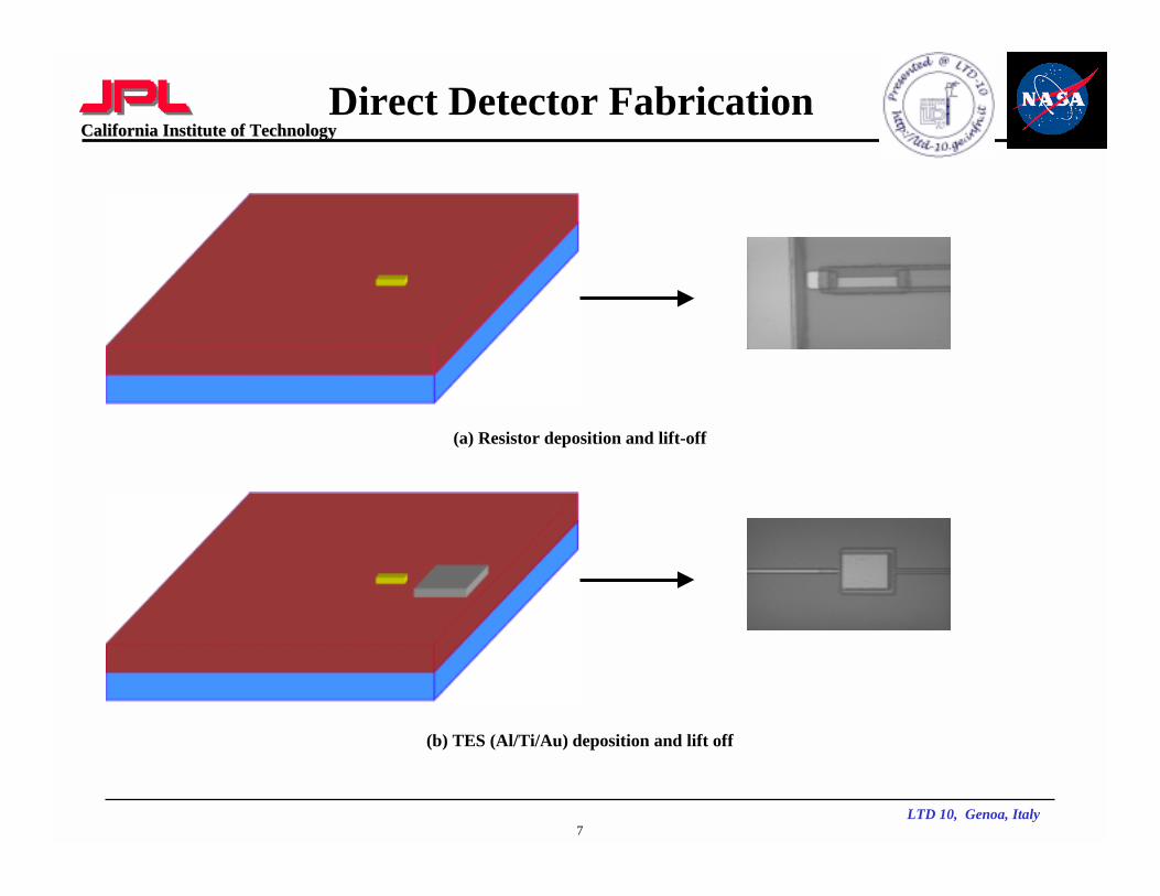
Direct Detector Fabrication
(a) Resistor deposition and lift-off
(b) TES (Al/Ti/Au) deposition and lift off

8
California Institute of TechnologyCalifornia Institute of Technology
LTD 10, Genoa, Italy
Direct Detector Fabrication
(c) The first SiO deposition to protect TES layers
(d) Nb Ground plane deposition and etch. Shunt resistor formation
9
California Institute of TechnologyCalifornia Institute of Technology
LTD 10, Genoa, Italy
Direct Detector Fabrication
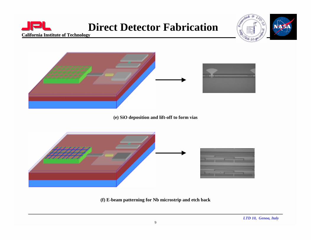
(e) SiO deposition and lift-off to form vias
(f) E-beam patterning for Nb microstrip and etch back

10
California Institute of TechnologyCalifornia Institute of Technology
LTD 10, Genoa, Italy
Direct Detector Fabrication
(g) Front, backside nitride etch and backside deep trench etch
(h) Top-view after final release and cleaning each array and double antenna-coupled Transition Edge Polarization-sensitive Bolometer
11
California Institute of TechnologyCalifornia Institute of Technology
LTD 10, Genoa, Italy
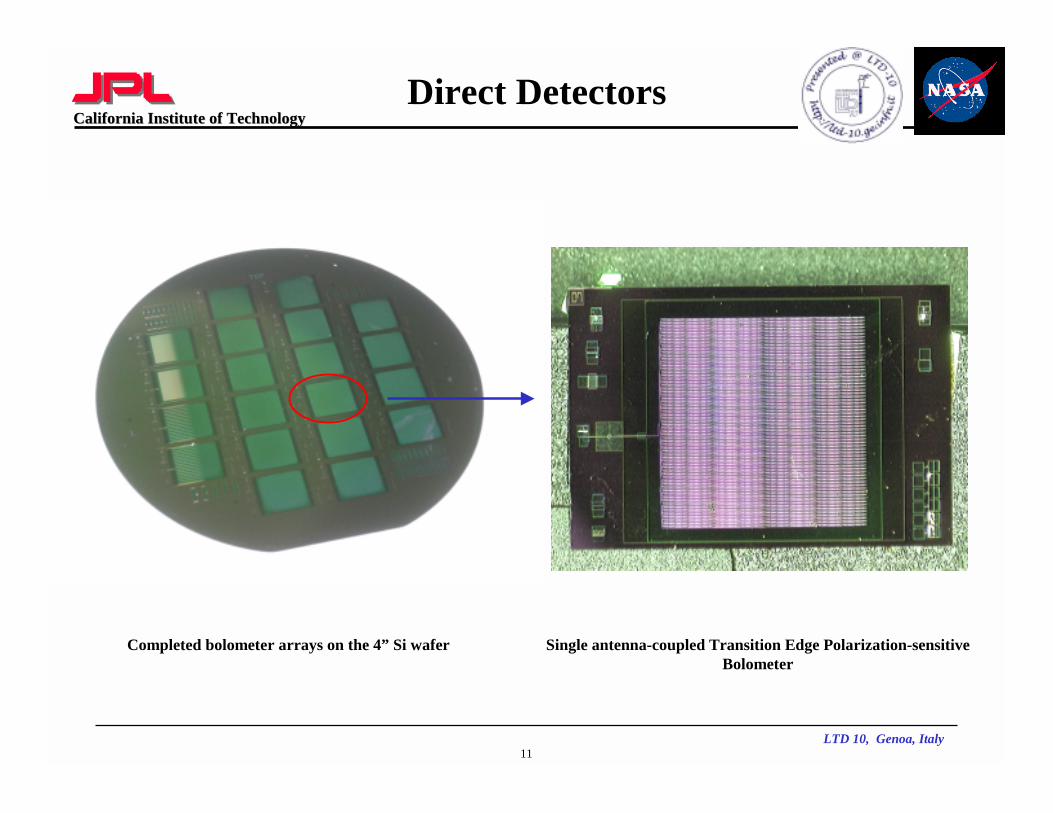
Direct Detectors
Completed bolometer arrays on the 4” Si wafer Single antenna-coupled Transition Edge Polarization-sensitive Bolometer

12
California Institute of TechnologyCalifornia Institute of Technology
LTD 10, Genoa, Italy
TES Temperatures
TES Temperatures Vs. Resistances
0
1
2
3
4
5
6
7
0.25 0.3 0.35 0.4 0.45 0.5
Temperature
Res
ista
nce
Al/Ti/Au = 220/280/220
Al/Ti/Au = 340/280/280
Al/Ti/Au = 280/280/340
Al/Ti/Au = 340/280/220
Figure. Transition temperatures as a function of Al/Au thicknesses
13
California Institute of TechnologyCalifornia Institute of Technology
LTD 10, Genoa, Italy
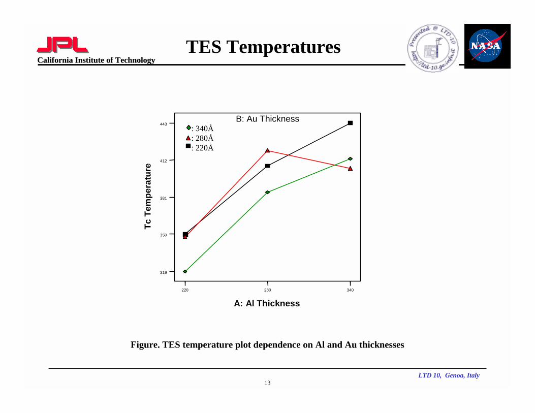
TES Temperatures
B: Au Thickness
A: Al Thickness
TcTe
mpe
ratu
re
220 280 340
319
350
381
412
443: 340Å: 280Å: 220Å
Figure. TES temperature plot dependence on Al and Au thicknesses

14
California Institute of TechnologyCalifornia Institute of Technology
LTD 10, Genoa, Italy
TES Layer Diffusion
Al/Ti/Au/Ti (28 nm/28 nm/28 nm/4 nm) at room temperature
Al/Ti/Au/Ti processed at 150 oC for 60 min
15
California Institute of TechnologyCalifornia Institute of Technology
LTD 10, Genoa, Italy
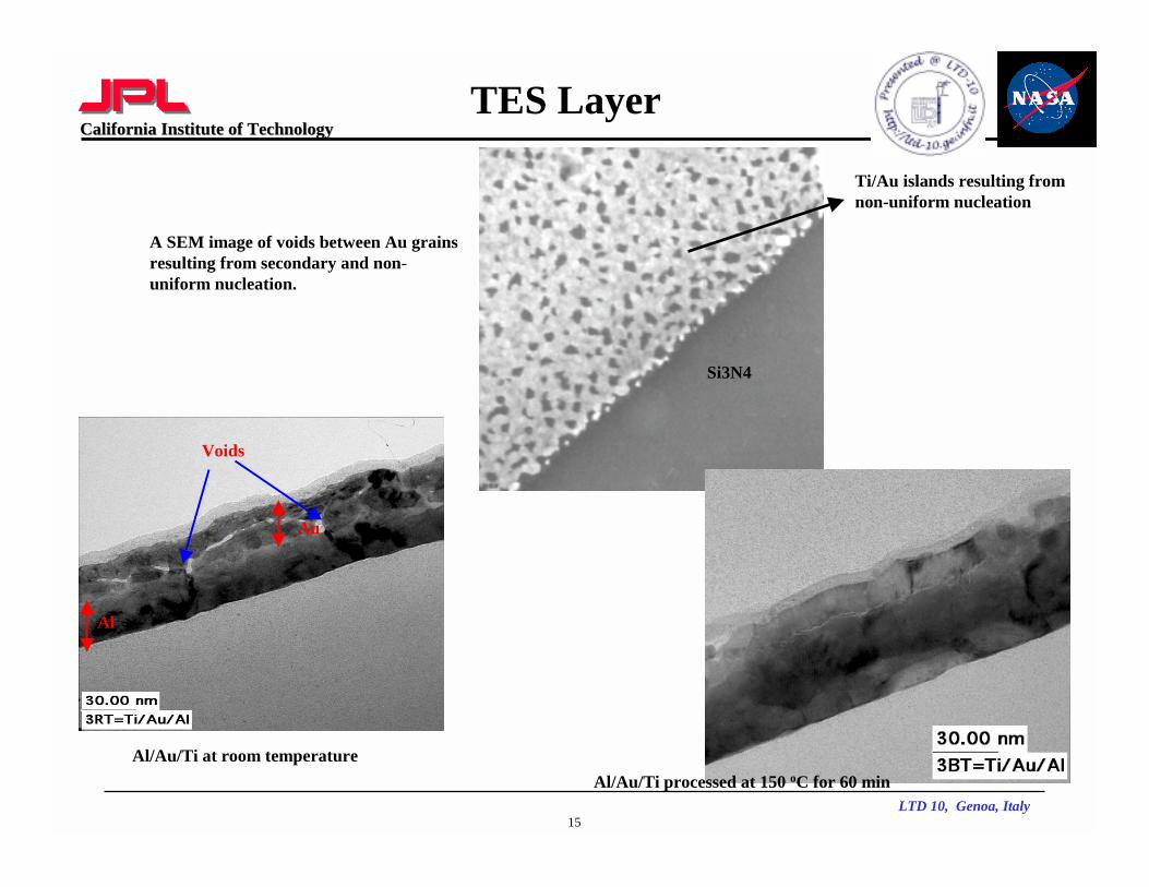
TES Layer
Al/Au/Ti at room temperature
Voids
Au
Al
Voids
Al/Au/Ti processed at 150 oC for 60 min
A SEM image of voids between Au grainsresulting from secondary and non-uniform nucleation.
Si3N4
Ti/Au islands resulting from non-uniform nucleation

16
California Institute of TechnologyCalifornia Institute of Technology
LTD 10, Genoa, Italy
Summary
• We have successfully fabricated antenna-coupled transition edge polarization-sensitive bolometer using micro-electro-mechanical systems (MEMS) techniques.
• Our Al/Ti/Au/Ti TES demonstrated excellent physical properties to help constant transition temperature during the operation.
• Using statistical engineering methods, we show that the factors important in the TES sensing temperature are, in decreasing order of importance, Al, Au thicknesses, and interaction between Al/Aulayers. We have demonstrated the use of an atomically thin Ti interlayer to prevent inter-diffusion between Al and Au layers. The Ti layer deposited at the interface also helps adhesion of a Au layer and avoids void formation. Ti layer contributes to hold down the change in transition temperature.
• We are testing the Nb microstrip antenna-coupled bolometer arrays for multi-color polarization-sensitive focal plane.

17
California Institute of TechnologyCalifornia Institute of Technology
LTD 10, Genoa, Italy
Acknowledgement
This research was performed at the Jet Propulsion Laboratory, an operating division of the California Institute of Technology, under a contract with the National Aeronautics and Space Administration.